JP2008171965A - Ultra-compact power converter - Google Patents
Ultra-compact power converterDownload PDFInfo
- Publication number
- JP2008171965A JP2008171965AJP2007002966AJP2007002966AJP2008171965AJP 2008171965 AJP2008171965 AJP 2008171965AJP 2007002966 AJP2007002966 AJP 2007002966AJP 2007002966 AJP2007002966 AJP 2007002966AJP 2008171965 AJP2008171965 AJP 2008171965A
- Authority
- JP
- Japan
- Prior art keywords
- magnetic induction
- main surface
- induction element
- coil
- electrode
- Prior art date
- Legal status (The legal status is an assumption and is not a legal conclusion. Google has not performed a legal analysis and makes no representation as to the accuracy of the status listed.)
- Withdrawn
Links
Images


Classifications
- H—ELECTRICITY
- H01—ELECTRIC ELEMENTS
- H01F—MAGNETS; INDUCTANCES; TRANSFORMERS; SELECTION OF MATERIALS FOR THEIR MAGNETIC PROPERTIES
- H01F17/00—Fixed inductances of the signal type
- H01F17/0006—Printed inductances
- H01F17/0033—Printed inductances with the coil helically wound around a magnetic core
- H—ELECTRICITY
- H01—ELECTRIC ELEMENTS
- H01L—SEMICONDUCTOR DEVICES NOT COVERED BY CLASS H10
- H01L23/00—Details of semiconductor or other solid state devices
- H01L23/58—Structural electrical arrangements for semiconductor devices not otherwise provided for, e.g. in combination with batteries
- H01L23/64—Impedance arrangements
- H01L23/645—Inductive arrangements
- H—ELECTRICITY
- H02—GENERATION; CONVERSION OR DISTRIBUTION OF ELECTRIC POWER
- H02M—APPARATUS FOR CONVERSION BETWEEN AC AND AC, BETWEEN AC AND DC, OR BETWEEN DC AND DC, AND FOR USE WITH MAINS OR SIMILAR POWER SUPPLY SYSTEMS; CONVERSION OF DC OR AC INPUT POWER INTO SURGE OUTPUT POWER; CONTROL OR REGULATION THEREOF
- H02M3/00—Conversion of DC power input into DC power output
- H02M3/003—Constructional details, e.g. physical layout, assembly, wiring or busbar connections
- H—ELECTRICITY
- H01—ELECTRIC ELEMENTS
- H01F—MAGNETS; INDUCTANCES; TRANSFORMERS; SELECTION OF MATERIALS FOR THEIR MAGNETIC PROPERTIES
- H01F17/00—Fixed inductances of the signal type
- H01F17/0006—Printed inductances
- H01F2017/0086—Printed inductances on semiconductor substrate
- H—ELECTRICITY
- H01—ELECTRIC ELEMENTS
- H01F—MAGNETS; INDUCTANCES; TRANSFORMERS; SELECTION OF MATERIALS FOR THEIR MAGNETIC PROPERTIES
- H01F27/00—Details of transformers or inductances, in general
- H01F27/28—Coils; Windings; Conductive connections
- H01F27/29—Terminals; Tapping arrangements for signal inductances
- H—ELECTRICITY
- H01—ELECTRIC ELEMENTS
- H01F—MAGNETS; INDUCTANCES; TRANSFORMERS; SELECTION OF MATERIALS FOR THEIR MAGNETIC PROPERTIES
- H01F27/00—Details of transformers or inductances, in general
- H01F27/40—Structural association with built-in electric component, e.g. fuse
- H—ELECTRICITY
- H01—ELECTRIC ELEMENTS
- H01L—SEMICONDUCTOR DEVICES NOT COVERED BY CLASS H10
- H01L2224/00—Indexing scheme for arrangements for connecting or disconnecting semiconductor or solid-state bodies and methods related thereto as covered by H01L24/00
- H01L2224/01—Means for bonding being attached to, or being formed on, the surface to be connected, e.g. chip-to-package, die-attach, "first-level" interconnects; Manufacturing methods related thereto
- H01L2224/10—Bump connectors; Manufacturing methods related thereto
- H01L2224/15—Structure, shape, material or disposition of the bump connectors after the connecting process
- H01L2224/16—Structure, shape, material or disposition of the bump connectors after the connecting process of an individual bump connector
- H01L2224/161—Disposition
- H01L2224/16151—Disposition the bump connector connecting between a semiconductor or solid-state body and an item not being a semiconductor or solid-state body, e.g. chip-to-substrate, chip-to-passive
- H01L2224/16221—Disposition the bump connector connecting between a semiconductor or solid-state body and an item not being a semiconductor or solid-state body, e.g. chip-to-substrate, chip-to-passive the body and the item being stacked
- H01L2224/16225—Disposition the bump connector connecting between a semiconductor or solid-state body and an item not being a semiconductor or solid-state body, e.g. chip-to-substrate, chip-to-passive the body and the item being stacked the item being non-metallic, e.g. insulating substrate with or without metallisation
- H—ELECTRICITY
- H01—ELECTRIC ELEMENTS
- H01L—SEMICONDUCTOR DEVICES NOT COVERED BY CLASS H10
- H01L2224/00—Indexing scheme for arrangements for connecting or disconnecting semiconductor or solid-state bodies and methods related thereto as covered by H01L24/00
- H01L2224/01—Means for bonding being attached to, or being formed on, the surface to be connected, e.g. chip-to-package, die-attach, "first-level" interconnects; Manufacturing methods related thereto
- H01L2224/26—Layer connectors, e.g. plate connectors, solder or adhesive layers; Manufacturing methods related thereto
- H01L2224/31—Structure, shape, material or disposition of the layer connectors after the connecting process
- H01L2224/32—Structure, shape, material or disposition of the layer connectors after the connecting process of an individual layer connector
- H01L2224/321—Disposition
- H01L2224/32151—Disposition the layer connector connecting between a semiconductor or solid-state body and an item not being a semiconductor or solid-state body, e.g. chip-to-substrate, chip-to-passive
- H01L2224/32221—Disposition the layer connector connecting between a semiconductor or solid-state body and an item not being a semiconductor or solid-state body, e.g. chip-to-substrate, chip-to-passive the body and the item being stacked
- H01L2224/32225—Disposition the layer connector connecting between a semiconductor or solid-state body and an item not being a semiconductor or solid-state body, e.g. chip-to-substrate, chip-to-passive the body and the item being stacked the item being non-metallic, e.g. insulating substrate with or without metallisation
- H—ELECTRICITY
- H01—ELECTRIC ELEMENTS
- H01L—SEMICONDUCTOR DEVICES NOT COVERED BY CLASS H10
- H01L2224/00—Indexing scheme for arrangements for connecting or disconnecting semiconductor or solid-state bodies and methods related thereto as covered by H01L24/00
- H01L2224/73—Means for bonding being of different types provided for in two or more of groups H01L2224/10, H01L2224/18, H01L2224/26, H01L2224/34, H01L2224/42, H01L2224/50, H01L2224/63, H01L2224/71
- H01L2224/732—Location after the connecting process
- H01L2224/73201—Location after the connecting process on the same surface
- H01L2224/73203—Bump and layer connectors
- H01L2224/73204—Bump and layer connectors the bump connector being embedded into the layer connector
- H—ELECTRICITY
- H01—ELECTRIC ELEMENTS
- H01L—SEMICONDUCTOR DEVICES NOT COVERED BY CLASS H10
- H01L23/00—Details of semiconductor or other solid state devices
- H01L23/48—Arrangements for conducting electric current to or from the solid state body in operation, e.g. leads, terminal arrangements ; Selection of materials therefor
- H01L23/488—Arrangements for conducting electric current to or from the solid state body in operation, e.g. leads, terminal arrangements ; Selection of materials therefor consisting of soldered or bonded constructions
- H01L23/498—Leads, i.e. metallisations or lead-frames on insulating substrates, e.g. chip carriers
- H01L23/49822—Multilayer substrates
- H—ELECTRICITY
- H01—ELECTRIC ELEMENTS
- H01L—SEMICONDUCTOR DEVICES NOT COVERED BY CLASS H10
- H01L2924/00—Indexing scheme for arrangements or methods for connecting or disconnecting semiconductor or solid-state bodies as covered by H01L24/00
- H01L2924/0001—Technical content checked by a classifier
- H01L2924/00011—Not relevant to the scope of the group, the symbol of which is combined with the symbol of this group
- H—ELECTRICITY
- H01—ELECTRIC ELEMENTS
- H01L—SEMICONDUCTOR DEVICES NOT COVERED BY CLASS H10
- H01L2924/00—Indexing scheme for arrangements or methods for connecting or disconnecting semiconductor or solid-state bodies as covered by H01L24/00
- H01L2924/0001—Technical content checked by a classifier
- H01L2924/00014—Technical content checked by a classifier the subject-matter covered by the group, the symbol of which is combined with the symbol of this group, being disclosed without further technical details
- H—ELECTRICITY
- H01—ELECTRIC ELEMENTS
- H01L—SEMICONDUCTOR DEVICES NOT COVERED BY CLASS H10
- H01L2924/00—Indexing scheme for arrangements or methods for connecting or disconnecting semiconductor or solid-state bodies as covered by H01L24/00
- H01L2924/19—Details of hybrid assemblies other than the semiconductor or other solid state devices to be connected
- H01L2924/191—Disposition
- H01L2924/19101—Disposition of discrete passive components
- H01L2924/19102—Disposition of discrete passive components in a stacked assembly with the semiconductor or solid state device
- H01L2924/19103—Disposition of discrete passive components in a stacked assembly with the semiconductor or solid state device interposed between the semiconductor or solid-state device and the die mounting substrate, i.e. chip-on-passive
- H—ELECTRICITY
- H01—ELECTRIC ELEMENTS
- H01L—SEMICONDUCTOR DEVICES NOT COVERED BY CLASS H10
- H01L2924/00—Indexing scheme for arrangements or methods for connecting or disconnecting semiconductor or solid-state bodies as covered by H01L24/00
- H01L2924/19—Details of hybrid assemblies other than the semiconductor or other solid state devices to be connected
- H01L2924/191—Disposition
- H01L2924/19101—Disposition of discrete passive components
- H01L2924/19105—Disposition of discrete passive components in a side-by-side arrangement on a common die mounting substrate
Landscapes
- Engineering & Computer Science (AREA)
- Power Engineering (AREA)
- Microelectronics & Electronic Packaging (AREA)
- Physics & Mathematics (AREA)
- Condensed Matter Physics & Semiconductors (AREA)
- General Physics & Mathematics (AREA)
- Computer Hardware Design (AREA)
- Coils Or Transformers For Communication (AREA)
- Dc-Dc Converters (AREA)
- Semiconductor Integrated Circuits (AREA)
- Coils Of Transformers For General Uses (AREA)
Abstract
Translated fromJapaneseDescription
Translated fromJapaneseこの発明は、半導体集積回路(以下ICと記す)などの半導体素子(電子部品)と、コイルやコンデンサおよび抵抗などの受動部品で構成されるDC−DCコンバータなどの超小型電力変換装置に関する。 The present invention relates to a micro power converter such as a DC-DC converter including a semiconductor element (electronic component) such as a semiconductor integrated circuit (hereinafter referred to as IC) and passive components such as a coil, a capacitor, and a resistor.
近年、電子情報機器、特に携帯型の各種電子情報機器の普及が著しい。それらの電子情報機器は、電池を電源とするものが多く、DC−DCコンバータなどの電力変換装置を内蔵している。通常その電力変換装置は、スイッチング素子、整流素子、制御用ICなどの能動素子と、磁気部品、コンデンサ、抵抗などの受動素子の各個別部品とをセラミック基板やプラスチックなどのプリント基板などの上に実装することでハイブリッド型電源モジュールとして構成されている。 In recent years, electronic information devices, in particular, various portable electronic information devices have been widely used. Many of these electronic information devices use a battery as a power source, and incorporate a power conversion device such as a DC-DC converter. Normally, the power conversion device is composed of active elements such as switching elements, rectifier elements, and control ICs, and individual components of passive elements such as magnetic components, capacitors, and resistors on a printed circuit board such as a ceramic substrate or plastic. By mounting, it is configured as a hybrid power supply module.
前記した携帯用を含めた各種電子情報機器の小型、薄型、軽量化の要望に伴い、内蔵される電力変換装置の小型、薄型、軽量化の要求も強い。ハイブリッド型電源モジュールの小型化は、MCM(マルチチップモジュール)技術や、積層セラミック部品などの技術により進歩してきている。しかしながら、個別の部品を同一基板上に、並べて実装するため、電源モジュールの実装面積の縮小化が制限されている。特にインダクタやトランスなどの磁気部品は、集積回路と比較すると体積が非常に大きいために電子機器の小型、薄型化をはかる上で最大の制約となっている。 Along with the demands for reducing the size, thickness, and weight of various electronic information devices including the above-mentioned portable devices, there is a strong demand for reducing the size, thickness, and weight of built-in power conversion devices. Miniaturization of the hybrid power supply module has been advanced by technologies such as MCM (multi-chip module) technology and multilayer ceramic components. However, since individual components are mounted side by side on the same substrate, reduction of the mounting area of the power supply module is limited. In particular, magnetic parts such as inductors and transformers have a very large volume compared to an integrated circuit, which is the biggest restriction in reducing the size and thickness of electronic devices.
これら磁気部品の小型、薄型化に対する今後の方向としては、チップ部品として限りなく小さく、薄くし、面実装する方向と、シリコン基板上に薄膜で形成する方向の2つが考えられる。近年、半導体技術の適用により、半導体基板上に薄型のマイクロ磁気素子(コイル、トランス)を搭載した例も報告されている。
特に、平面型磁気部品として、スイッチング素子や制御回路などの半導体部品を作り込んだ半導体基板の表面上に、薄膜コイルを磁性基板とフェライト基板とで挟んだ形の平面型磁気部品(薄型インダクタ)を薄膜技術により形成したものが開示されている(例えば、特許文献1など)。
これにより、磁気素子の薄型化とその実装面積の削減が可能となった。しかし、真空プロセスでの製造でコストが高くなる。また、電流の大きい所で使用する場合などは、磁性膜と絶縁膜に関する多大な積層工程が必要であり、コストが非常に高くなるという問題があった。There are two possible future directions for miniaturization and thinning of these magnetic components: a chip component that is extremely small and thin, surface-mounted, and a thin film formed on a silicon substrate. In recent years, there has been reported an example in which a thin micromagnetic element (coil, transformer) is mounted on a semiconductor substrate by application of semiconductor technology.
In particular, as a planar magnetic component, a planar magnetic component (thin inductor) in which a thin film coil is sandwiched between a magnetic substrate and a ferrite substrate on the surface of a semiconductor substrate on which semiconductor components such as switching elements and control circuits are built. Are formed by thin film technology (for example, Patent Document 1).
As a result, the magnetic element can be made thinner and its mounting area can be reduced. However, the manufacturing cost is increased in the vacuum process. In addition, when used in a place with a large current, a large number of lamination steps relating to the magnetic film and the insulating film are required, and there is a problem that the cost becomes very high.
平面型磁気素子としてスパイラル(渦巻き状)のコイル導体の隙間に磁性を帯びた微粒子を混入した樹脂を充填し、上面、下面をフェライト基板で挟み込んで形成したものが開示されている(例えば、特許文献2など)。
この方法では、コイル導体のインダクタンスは、スパイラルの回数(ターン数)にほぼ比例するため、大きなインダクタンスを得るためには、ターン数を増やす必要がある。実装面積を増やさずにターン数を増やすと、コイル導体の断面積を小さくする必要がある。つまり、大きなインダクタンスを得るためには、コイル導体の断面積を小さく、導体線長を長くしなければならない。しかし、コイル断面積を小さく、導体線長を長くすると、コイル導体の直流抵抗が増大するため電力損失が増大してしまうという課題があった。A planar magnetic element is disclosed in which a gap between spiral coil conductors is filled with a resin mixed with magnetic particles and the upper and lower surfaces are sandwiched between ferrite substrates (for example, patents). Reference 2).
In this method, since the inductance of the coil conductor is substantially proportional to the number of spirals (turns), it is necessary to increase the number of turns in order to obtain a large inductance. If the number of turns is increased without increasing the mounting area, it is necessary to reduce the cross-sectional area of the coil conductor. That is, in order to obtain a large inductance, the coil conductor must have a small cross-sectional area and a long conductor wire length. However, when the coil cross-sectional area is reduced and the conductor wire length is increased, the DC resistance of the coil conductor is increased, resulting in an increase in power loss.
その点を解消するために、磁性絶縁基板と、該磁性絶縁基板の第1主面に形成された第1導体と前記磁性絶縁基板の第2主面に形成された第2導体と前記磁性絶縁基板を貫通する貫通孔に形成された接続導体とをそれぞれ接続してなるソレノイド状のコイル導体と、からなる薄型磁気素子が開示されている(例えば、特許文献3など)。
この特許文献3に記載されている構造は、磁性絶縁基板に貫通孔を形成し、コイル導体を形成する際、同時に半導体素子や、実装基板などと接続するための実装端子を形成し、コイルとなる磁性絶縁基板にICを実装するだけで、新たな実装基板を不要とし、超小型・薄型の電力変換装置を実現するものである。In order to solve the problem, a magnetic insulating substrate, a first conductor formed on the first main surface of the magnetic insulating substrate, a second conductor formed on the second main surface of the magnetic insulating substrate, and the magnetic insulation. There has been disclosed a thin magnetic element comprising solenoidal coil conductors connected to connecting conductors formed in through holes penetrating a substrate (for example, Patent Document 3).
In the structure described in Patent Document 3, when a through hole is formed in a magnetic insulating substrate and a coil conductor is formed, a mounting terminal for connecting to a semiconductor element, a mounting substrate, or the like is formed at the same time. By simply mounting an IC on a magnetic insulating substrate, a new mounting substrate is unnecessary, and an ultra-small and thin power conversion device is realized.
特許文献3に記載されている超小型電力変換素子の特徴は、磁性絶縁基板に貫通孔を形成し、その貫通孔を通して電気的に接続されたコイル導体を第1主面、第2主面に具備し、さらに同様に第1主面に半導体素子との電気的接続をするための電極(接合単端子)、第2主面に実際に使用される場合のプリント板などとの電気的接続のための電極(実装電極)を具備している薄型磁気誘導素子を有することである。この構造を適用することにより、デバイスを構成する部品を最小限に留め、薄型化を実現した超小型電力変換装置を得ることができる。この超小型電力変換装置について説明する。 The feature of the micro power conversion element described in Patent Document 3 is that a through hole is formed in a magnetic insulating substrate, and a coil conductor electrically connected through the through hole is formed on the first main surface and the second main surface. In addition, similarly, an electrode (junction single terminal) for electrical connection with a semiconductor element on the first main surface, and an electrical connection with a printed board when actually used on the second main surface A thin magnetic induction element having an electrode for mounting (mounting electrode). By applying this structure, it is possible to obtain an ultra-compact power conversion device that minimizes the number of parts constituting the device and achieves a reduction in thickness. This micro power converter will be described.
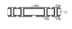
図15は、従来の超小型電力変換装置の構成図であり、同図(a)はICチップを搭載した薄膜磁気誘導素子の要部断面図、同図(b)は薄型磁気誘導素子の第1主面(表面)から透視した要部平面図である。同図(a)は同図(b)のY−Y線で切断した要部断面図である。また、同図(b)ではICチップ80を点線で示した。
従来の薄型磁気誘導素子300は、フェライト基板86の中央部にソレノイド状コイルが形成され、周辺部に電極82、88が形成されている。ソレノイド状コイルはフェライト基板86の第1主面と第2主面と貫通孔85に形成されるコイル導体84(接続導体も含んでいる)で出来ている。電極82は第1主面、電極88は第2主面に形成され,貫通孔83に形成される接続導体83aで互いに接続されている。15A and 15B are configuration diagrams of a conventional ultra-small power converter, in which FIG. 15A is a cross-sectional view of a main part of a thin-film magnetic induction element mounted with an IC chip, and FIG. It is the principal part top view seen through from 1 main surface (surface). FIG. 6A is a cross-sectional view of the main part taken along line YY in FIG. In FIG. 2B, the
In the conventional thin
第1主面に形成された電極82とICチップ80はスタッドバンプ81を介して固着し、ICチップ80とフェライト基板86の間にはアンダーフィル樹脂89が充填されている。また、第2主面に形成されたコイル導体84は保護膜87で被覆されている。
また、超小型電力変換装置ではないが、コイル導体および磁性材料からなるコイルが内部に形成され、回路部品を搭載するための外部電極が上面に形成され、当該外部電極と前記コイルとの配線を行うための配線パターンを内部に設けることにより、搭載する回路部品の配置の自由度を高めた積層基板が開示されている(例えば、特許文献4など)。
Although not a micro power converter, a coil made of a coil conductor and a magnetic material is formed inside, an external electrode for mounting a circuit component is formed on the top surface, and wiring between the external electrode and the coil is provided. There has been disclosed a laminated substrate in which a wiring pattern for performing is provided inside to increase the degree of freedom of arrangement of circuit components to be mounted (for example, Patent Document 4).
前述した特許文献3の構造では、図15に示したように、薄型磁気誘導素子の外周部に半導体素子であるICチップ80との接合電極(電極82)がある。これは薄型磁気誘導素子のコイルの形状がソレノイド状であるために、磁気誘導素子の中央部にコイルを配置しなければならないためで、必然的にICチップ80などの半導体素子との接合電極は、薄型磁気誘導素子の外周部に配置しなければならなくなる。 In the structure of Patent Document 3 described above, as shown in FIG. 15, there is a bonding electrode (electrode 82) to the
薄型磁気誘導素子の特性のうちインダクタンス値は、磁気誘導素子のサイズに大きく依存するために、必要な特性を得るためには磁気誘導素子のサイズの制限が非常に大きい。
一方、半導体素子のサイズについては、特性でサイズが制限されることはもちろんであるが、機能によってサイズを大幅に低減できる場合もある。
従って、半導体素子と薄型磁気誘導素子のサイズには本来相関はないが、本構造の場合には、半導体素子を薄型磁気誘導素子に面実装することと、電極82が外周に配置されていることから、半導体素子のサイズが薄型磁気誘導素子のサイズによって制限されてしまうという問題があった。Among the characteristics of the thin magnetic induction element, the inductance value greatly depends on the size of the magnetic induction element. Therefore, the size of the magnetic induction element is extremely limited in order to obtain necessary characteristics.
On the other hand, as for the size of the semiconductor element, the size is of course limited by the characteristics, but the size may be greatly reduced depending on the function.
Accordingly, the size of the semiconductor element and the thin magnetic induction element is not originally correlated, but in the case of this structure, the semiconductor element is surface-mounted on the thin magnetic induction element and the
このため、半導体素子の小型化が可能であっても、薄型磁気誘導素子の小型化ができない場合は、半導体素子はサイズを大きくしなければならず、コスト低減を妨げる要因になっていた。
また、電極82が外周に配置されていることから、複数の半導体素子を実装することが困難であり、薄型磁気誘導素子ひとつに対して、実装できる半導体素子はひとつという制限もあり、多機能化の妨げとなっていた。For this reason, even if the semiconductor element can be reduced in size, if the thin magnetic induction element cannot be reduced in size, the semiconductor element has to be increased in size, which has been a factor hindering cost reduction.
In addition, since the
また、特許文献4の積層基板は、内部に形成されたコイル(インダクタ)に接続される部品の配置の自由度はあるものの、複雑な構成であり、コストおよび超小型化には問題のある構造となっている。
この発明の目的は、前記の課題を解決して、薄型磁気誘導素子より小さな半導体素子を含む部品を薄型磁気誘導素子の外周部に形成された電極の位置に制約されずに薄型磁気誘導素子上の所定の位置に面実装できる超小型電力変換装置を提供することである。In addition, the multilayer substrate of
The object of the present invention is to solve the above-mentioned problems and to allow a part including a semiconductor element smaller than the thin magnetic induction element to be placed on the thin magnetic induction element without being restricted by the position of the electrode formed on the outer peripheral portion of the thin magnetic induction element. It is an object of the present invention to provide a micro power converter that can be surface-mounted at a predetermined position.
前記の目的を達成するために、半導体集積回路が形成された半導体基板と薄型磁気誘導素子とコンデンサを有し、前記薄型磁気誘導素子が磁性絶縁基板と該磁性絶縁基板の中央部に形成されたコイルと該磁性絶縁基板の第1主面および第2主面の外周部で貫通孔を介して電気的に接続された電極を有する超小型電力変換装置において、前記第1主面のコイル形成領域上に絶縁層を介して一端が前記電極と接続して形成された配線を有する構成とする。 In order to achieve the above object, a semiconductor substrate on which a semiconductor integrated circuit is formed, a thin magnetic induction element, and a capacitor are provided, and the thin magnetic induction element is formed at a central portion of the magnetic insulating substrate and the magnetic insulating substrate. In a micro power converter having an electrode electrically connected via a through-hole at the outer periphery of the first main surface and the second main surface of the magnetic insulating substrate, the coil forming region of the first main surface One end of the wiring is connected to the electrode via an insulating layer.
また、前記コイルが、前記磁性絶縁基板の第1主面に形成された第1導体と前記磁性絶縁基板の第2主面に形成された第2導体と前記磁性絶縁基板を貫通する貫通孔に形成された接続導体とをそれぞれに接続してなるソレノイド状コイルであるとよい。
また、前記配線の他端に半導体素子を含む部品を接続する構成とするとよい。
また、前記磁性絶縁基板がフェライト基板であるとよい。Further, the coil is formed in a first conductor formed on the first main surface of the magnetic insulating substrate, a second conductor formed on the second main surface of the magnetic insulating substrate, and a through hole penetrating the magnetic insulating substrate. It is good to be a solenoidal coil formed by connecting the formed connection conductors to each other.
Further, it is preferable that a component including a semiconductor element is connected to the other end of the wiring.
The magnetic insulating substrate may be a ferrite substrate.
この発明によれば、薄型磁気誘導素子を構成するコイル導体上に絶縁膜を介して配線を形成し、この配線に所定の大きさの半導体素子を含む部品を面実装(固着)することで、部品のサイズを制限することがなくなり、部品のコスト低減を図ることができ、超小型電力変換装置のコストを低減させることができる。 According to the present invention, a wiring is formed on the coil conductor constituting the thin magnetic induction element via the insulating film, and a component including a semiconductor element of a predetermined size is surface-mounted (adhered) to the wiring. The size of the component is not limited, the cost of the component can be reduced, and the cost of the micro power converter can be reduced.
実施の形態を以下の実施例で説明する。 Embodiments will be described in the following examples.
図1および図2は、この発明の第1実施例の超小型電力変換装置の構成図であり、図1(a)は薄型磁気誘導素子の第1主面から透視した要部平面図、図1(b)は図1(a)のY−Y線で切断したときの要部断面図であり、図2(a)は半導体素子を面実装した薄型磁気誘導素子の要部平面図であり、図2(b)は図2(a)のY−Y線で切断した要部断面図である。図2の半導体素子21は電源制御部などが集積された電源ICなどである。 FIG. 1 and FIG. 2 are configuration diagrams of a micro power conversion device according to a first embodiment of the present invention. FIG. 1 (a) is a plan view of a main part seen through the first main surface of a thin magnetic induction element. 1 (b) is a cross-sectional view of the main part when cut along the YY line in FIG. 1 (a), and FIG. 2 (a) is a plan view of the main part of a thin magnetic induction element having a semiconductor element mounted thereon. FIG. 2B is a cross-sectional view of the main part taken along the line YY of FIG. The
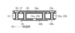
この薄型磁気誘導素子100の構成は、貫通孔12a、13aを形成した磁性絶縁基板11に第1主面および第2主面のコイル導体16a、16bと電極15a、電極15bをそれぞれ形成し、コイル導体16aと16bを貫通孔13aに形成された接続導体13bで、電極15aと15bを貫通孔12aに形成された接続導体12bでそれぞれ接続するとともに、第1主面のコイル導体16aの上に絶縁層17を形成し、第1主面の電極15a上の絶縁層17に開口部33を設け、その開口部33を介して電極15aと電気的に接続する配線14を絶縁層17上に形成する。配線14は配線部14aとパッド電極部14bおよび接続電極部14cとを有し、接続電極部14cは電極15aと接続し、パッド電極部14bは半導体素子21に形成した図示しない電極(パッド電極)と接続する実装電極の役割をする。従って、パッド電極部14bの配置は半導体素子21に形成した電極(パッド電極)の配置に合わせて形成する必要がある。また、配線14は配線部14aとパッド電極部14bおよび接続電極部14cのそれぞれの幅を点線14dで示したように全て同じにしても構わない。この場合もパッド電極部14bに相当する箇所の配置は半導体素子21に形成した電極の配置に合わせる必要がある。 The thin
尚、第2主面の18はコイル導体16bに対する保護膜である。
この構成とすることで、薄型磁気誘導素子100のサイズや電極15aの位置に左右されることなく、半導体素子21のサイズ(チップサイズのこと)や半導体素子21の電極位置を任意に設定することができる。このため、半導体素子21のサイズの小型化が薄型磁気誘導素子100の大きさ(フェライト基板11の大きさ)に左右されずに可能となる。半導体素子21のサイズを小さくすることで、超小型電力変換装置の低コスト化を図ることができる。In addition, 18 of the 2nd main surface is a protective film with respect to the
By adopting this configuration, the size of the semiconductor element 21 (chip size) and the electrode position of the
図3〜図12は、図1の薄型磁気誘導素子100の製造工程を説明するための製造工程順に示した要部製造工程断面図である。尚、図3〜図12は図1(b)の断面図に相当する要部断面図である。図3〜図12は、1つの薄型磁気誘導素子片のみについて拡大して示してあるが、実際はこのような薄型磁気誘導素子片を大きなフェライト基板11に多数形成し、最終的に図示しないスクライブラインに沿って大きなフェライト基板11を切断して1つの薄型磁気誘導素子100となる。つぎにその詳細を説明する。 3 to 12 are cross-sectional views of the main part manufacturing process shown in the order of the manufacturing process for explaining the manufacturing process of the thin
磁性絶縁基板としては、厚さ525μmのNi−Zn系フェライト基板11を用いた。尚、フェライト基板11の厚さは必要なインダクタンス、コイル電流値、フェライト基板11である磁性絶縁基板の特性から決定されるものであり、今回の実施例での厚さに限ったものではなく、絶縁性の磁性基板であればどの材料でも良い。今回は、基板状に容易に成型し得る材料としてフェライト基板11を用いた。 As the magnetic insulating substrate, a Ni—
まず、フェライト基板11に貫通孔12a、13aを形成する(図3)。貫通孔12aは第1主面の電極15aと第2主面の電極15bを接続するのに用いられ、貫通孔13aは第1主面のコイル導体16aと第2主面のコイル導体16bを接続するのに用いられる。加工方法は、レーザ加工、サンドブラスト加工、放電加工、超音波加工、機械加工などいずれの方法も適用でき、加工コスト、加工寸法などで決定する必要がある。今回の実施例では、貫通孔12a、13aの最小加工寸法幅が0.13mmと微小なこと、加工箇所が多いことからサンドブラスト法を用いた。 First, the through
つぎに、貫通孔12a、13aとフェライト基板11の第1主面、第2主面に、接続導体12b、13bとコイル導体16a、16bおよび電極15a、15bをそれぞれ同時に形成する。つぎにその詳細を説明する。
まず、フェライト基板11全面に導電性を付与するために、Cr/Cuをスパッタ法で成膜し、めっきシード層31を形成する(図4)。このとき、貫通孔12a、13aの側壁へも導電性は付与されるが、必要であれば、無電解めっきなどを施しても良い。また、スパッタ法にかぎらず真空蒸着法、CVD(ケミカルベイパーデポジション)法、などを用いても良い。無電解めっきのみで形成する方法でも良い。ただし、フェライト基板11との密着性を十分得られる方法が望ましい。なお、導電性材料については導電性を持つ材料であればなんでも良い。密着性を得るための密着層として今回はCrを用いたが、Ti、W、Nb、Taなども用いることができる。また、Cuが後工程の電解めっき工程でめっきが生成されるめっきシード層31となるが、Cu以外にもNi、Auなどを用いることができる。今回は、後工程での加工の容易さも考慮し、Cr/Cuの膜構成とした。Next, the
First, in order to impart conductivity to the entire surface of the
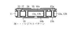
つぎに、第1主面、第2主面に形成されるべきコイル導体16a、16b、電極15a、15bのパターンをフォトレジストを用いて形成する。本実施例ではネガ型のフィルムタイプのフォトレジストを用いてこれらのレジストパターン32を形成する(図5)。
つぎに、レジストパターン32の開口部へ電解めっきで導電層34であるCuを形成させる(図6)。このとき、貫通孔12a、13aへもCuがめっきされて、接続導体12b、13bが同時に形成される。接続導体13aによって第1主面と第2主面のコイル導体16a、16bが接続されて、ソレノイド状コイルが形成される。また、電極15a、15bも同時に形成され、接続導体12aでそれぞれが接続される。電解めっき後、レジストパターン32を除去し、その後で不要なめっきシード層31を除去することで、所望のコイル導体16a,16bと電極15a、15bが形成される(図7)。Next, patterns of the
Next, Cu which is the
つぎに、コイル導体16aが形成される第1主面には電極15aが部分的に露出するように絶縁膜17を形成し、コイル導体16bが形成される第2主面には電極15bを除きその他の箇所に保護膜18を形成する(図8)。本実施例では両者ともフィルム型の感光性絶縁材料を用いた。絶縁層17はコイル導体16aとその上部に配置される配線14(配線パターン)とを電気的に絶縁する層間絶縁膜の役割を果たし、保護膜18は、第2主面のコイル導体16bを保護する役割を果たす。また、この両者(絶縁膜16および保護膜18)は貫通孔12a,13aの内部を充填する機能も持つ。コイル導体16a、16bは複雑な凹凸構造であるために、十分導体間を埋め込み、かつ貫通孔12a、13aの内部もボイドなく埋め込むために、両者には真空ラミネート法を用いた。 Next, the insulating
また、両者の形成は感光性であるため、通常のフォトレジストのように露光、現像を実施し、絶縁層17には開口部33も同時に形成した。使用した感光性絶縁材料は熱硬化型であるため、加工後に180℃で熱硬化した。なお、絶縁層17や保護膜18の形成方法はフィルム型の材料に限定されるものではなく、液状の絶縁材料をスクリーン印刷でパターン形成し、熱硬化させても良い。 In addition, since the formation of both was photosensitive, exposure and development were carried out like a normal photoresist, and the
つぎに絶縁層17上にスパッタ法で導電膜35であるAl膜を1μm成膜した(図9)。今回はスパッタ法を用いたが、手法は蒸着法、CVD法など、どのような手法でも良いが、第1主面の電極15aとの密着性が十分得られる手法を選択する必要がある。密着性を得るために、導電膜35の下部に密着層を成膜するなども必要に応じて取る。本実施例では、導電膜35であるAl膜の下にCrを0.2μm成膜し、密着性を向上させている。また、配線抵抗が特性に影響を与える場合には、成膜時の膜厚を厚くするか、めっきなどの手法を用いてさらに導電膜35であるAl膜の膜厚を厚くする手法を取る必要がある。導電膜35(配線材料)には、Al以外の材料を用いても良いが、後工程での半導体素子21との接続工程に対応できる材料を選択し、且つ、配線14の加工を考慮して選択する。本実施例では、超音波接合を用いるためにAlを選択した。 Next, 1 μm of an Al film as the
つぎに、導電膜35を加工するためのレジストパターン36を形成し(図10)、ウェットエッチングで導電膜35を所望の形状に加工し(図11)、その後レジストを剥離して薄型磁気誘導素子100の配線14を形成する(図12)。
上記工程で、薄型磁気誘導素子100を製作した。このあと、図2に示すように、スタッドバンプ22を用いた超音波接合法により半導体素子21と接続し、半導体素子21と薄型磁気誘導素子100の間をアンダーフィル樹脂23で封止し、図示しないコンデンサなど接続して超小型電力変換装置が完成する。接続方法として本実施例ではスタッドバンプ22と超音波接合を用いたが、これに限定されるものではなく、はんだ接合、導電接着材などを用いても問題はない。また、半導体素子21と薄型磁気誘導素子100の固定にはアンダーフィル樹脂23を用いたが、これは必要に応じて材料を選定すれば良く、エポキシ樹脂などの封止材などでも良い。Next, a resist
The thin
本実施例では、薄型磁気誘導素子100の外形が3.5mm×3.5mmのものを用いた。これと同じ大きさの図15に示す従来の薄型磁気誘導素子300を用いた場合には、半導体素子80と接続する電極82が外周部に配置されているため、半導体素子80のサイズは3.0mm×3.0mm程度までしか小さくすることができず、それ以上小さくするためには、薄型磁気誘導素子300の大きさを小さくしなければならず、特性を悪化させてしまう。 In this embodiment, the thin
第1実施例では、薄型磁気誘導素子100を小さくすることなく、面実装する半導体素子21のみ小さくできる。具体的には所望される半導体素子21のサイズである2.0mm×2.0mmまで小さくすることができ、半導体素子21のコスト低減効果は、4/9(面積比)であり、大幅なコスト低減効果が得られた。 In the first embodiment, only the
図13および図14は、この発明の第2実施例の超小型電力変換装置の構成図であり、図13は薄型磁気誘導素子200を第1主面から透視した要部平面図、図14は図13の薄型磁気誘導素子200の配線に半導体素子とコンデンサを固着し面実装した要部平面図である。
第2実施例では、部品として1個の半導体素子21と3個のコンデンサ41を薄型磁気誘導素子200上の絶縁層17上に形成した配線14に固着して面実装した例を示した。この部品の個数は超小型電力変換装置に付与する機能によって増減するのは勿論である。FIGS. 13 and 14 are configuration diagrams of a micro power conversion device according to a second embodiment of the present invention. FIG. 13 is a plan view of a main part of the thin
In the second embodiment, an example is shown in which one
従来の外周電極構造では、実装する半導体素子のサイズに制限があるため、所望の特性を持つ素子を複数実装することは困難であった。
しかし、本発明により、必要な配線14を必要な形状、位置で薄型磁気誘導素子200上に形成することができるため、部品サイズの制限もなく、実装する部品数も増加させることができる。これにより、要求機能が複雑になり、複数の部品が必要な場合でも、問題なく構造を製作することができる。In the conventional outer peripheral electrode structure, since the size of the semiconductor element to be mounted is limited, it is difficult to mount a plurality of elements having desired characteristics.
However, according to the present invention, since the
このように、半導体素子21を含む複数の部品を薄型磁気誘導素子200に面実装させることで、超小型電力変換装置の外形を大きくすることなく機能向上を図ることができる。
尚、第1、第2実施例において、コイルとしてソレノイド形状コイルを一例として挙げたが、本発明においては、コイル形成は関係なく、渦巻き形状(スパイラル形状)など別の形状のコイルについても適用できる。As described above, by mounting a plurality of components including the
In the first and second embodiments, the solenoid-shaped coil is exemplified as the coil. However, in the present invention, the coil formation is not related, and the coil can be applied to a coil having a different shape such as a spiral shape (spiral shape). .
11 フェライト基板
12a 貫通孔(電極部)
12b 接続導体(電極部)
13a 貫通孔(コイル導体部)
13b 接続導体(コイル導体部)
14 配線
14a 配線部
14b パッド電極部
14c 接続電極部
14d 配線部、電極部および接続電極部における幅を等しくした場合の配線
15a 電極(第1主面)
15b 電極(第2主面)
16a コイル導体(第1主面)
16b コイル導体(第2主面)
17 絶縁層
18 保護膜
21 半導体素子
22 スタッドバンプ
23 アンダーフィル樹脂
31 めっきシード層
32、36 レジストパターン
33 開口部
34 導電層
35 導電膜
100、200 薄型磁気誘導素子
11
12b Connecting conductor (electrode part)
13a Through hole (coil conductor part)
13b Connection conductor (coil conductor)
14 Wiring
15b Electrode (second main surface)
16a Coil conductor (first main surface)
16b Coil conductor (second main surface)
DESCRIPTION OF
Claims (4)
Translated fromJapanesePriority Applications (4)
| Application Number | Priority Date | Filing Date | Title |
|---|---|---|---|
| JP2007002966AJP2008171965A (en) | 2007-01-11 | 2007-01-11 | Ultra-compact power converter |
| CN2008100015162ACN101266868B (en) | 2007-01-11 | 2008-01-04 | Ultra-small electric power conversion device |
| US11/972,609US8018311B2 (en) | 2007-01-11 | 2008-01-10 | Microminiature power converter |
| DE102008003952ADE102008003952A1 (en) | 2007-01-11 | 2008-01-11 | Microminiature inverter |
Applications Claiming Priority (1)
| Application Number | Priority Date | Filing Date | Title |
|---|---|---|---|
| JP2007002966AJP2008171965A (en) | 2007-01-11 | 2007-01-11 | Ultra-compact power converter |
Publications (1)
| Publication Number | Publication Date |
|---|---|
| JP2008171965Atrue JP2008171965A (en) | 2008-07-24 |
Family
ID=39510098
Family Applications (1)
| Application Number | Title | Priority Date | Filing Date |
|---|---|---|---|
| JP2007002966AWithdrawnJP2008171965A (en) | 2007-01-11 | 2007-01-11 | Ultra-compact power converter |
Country Status (4)
| Country | Link |
|---|---|
| US (1) | US8018311B2 (en) |
| JP (1) | JP2008171965A (en) |
| CN (1) | CN101266868B (en) |
| DE (1) | DE102008003952A1 (en) |
Families Citing this family (15)
| Publication number | Priority date | Publication date | Assignee | Title |
|---|---|---|---|---|
| US20110050334A1 (en)* | 2009-09-02 | 2011-03-03 | Qualcomm Incorporated | Integrated Voltage Regulator with Embedded Passive Device(s) |
| US9048112B2 (en) | 2010-06-29 | 2015-06-02 | Qualcomm Incorporated | Integrated voltage regulator with embedded passive device(s) for a stacked IC |
| DE102010052401A1 (en)* | 2010-11-24 | 2012-05-24 | Giesecke & Devrient Gmbh | Circuit arrangement for portable data carriers |
| JP2012233738A (en)* | 2011-04-28 | 2012-11-29 | Mitsubishi Electric Corp | Instrument transformer |
| US9070642B2 (en) | 2011-09-14 | 2015-06-30 | Infineon Technologies Ag | Electronic module |
| JP2014154813A (en)* | 2013-02-13 | 2014-08-25 | Ibiden Co Ltd | Printed wiring board |
| US9935166B2 (en) | 2013-03-15 | 2018-04-03 | Qualcomm Incorporated | Capacitor with a dielectric between a via and a plate of the capacitor |
| US9634640B2 (en) | 2013-05-06 | 2017-04-25 | Qualcomm Incorporated | Tunable diplexers in three-dimensional (3D) integrated circuits (IC) (3DIC) and related components and methods |
| JP6312997B2 (en)* | 2013-07-31 | 2018-04-18 | 新光電気工業株式会社 | Coil substrate, manufacturing method thereof, and inductor |
| JP2015138935A (en)* | 2014-01-24 | 2015-07-30 | イビデン株式会社 | Printed wiring board |
| US10050528B2 (en)* | 2015-06-29 | 2018-08-14 | Infineon Technologies Austria Ag | Current distribution in DC-DC converters |
| CN107046366B (en) | 2016-02-05 | 2019-06-04 | 台达电子企业管理(上海)有限公司 | Supply convertor and preparation method thereof |
| US9911720B1 (en) | 2016-08-19 | 2018-03-06 | Infineon Technologies Americas Corp. | Power switch packaging with pre-formed electrical connections for connecting inductor to one or more transistors |
| CN106601728A (en)* | 2016-11-04 | 2017-04-26 | 苏州青新方电子科技有限公司 | Three-dimensional laminated integrated device of three-dimensional laminated inductive element and wafer chip, and manufacturing method and application thereof |
| CN110808150A (en)* | 2019-12-02 | 2020-02-18 | 旺诠科技(昆山)有限公司 | Inductance assembly with down-leading type electrode and processing method thereof |
Family Cites Families (21)
| Publication number | Priority date | Publication date | Assignee | Title |
|---|---|---|---|---|
| JPS63193896A (en)* | 1987-02-06 | 1988-08-11 | 株式会社東芝 | thin film electromagnetic transducer |
| JP3286106B2 (en)* | 1995-03-01 | 2002-05-27 | 株式会社日立製作所 | Switching power supply |
| JP3167936B2 (en)* | 1996-08-08 | 2001-05-21 | 三菱電機株式会社 | Power converter |
| US6240622B1 (en)* | 1999-07-09 | 2001-06-05 | Micron Technology, Inc. | Integrated circuit inductors |
| JP3767296B2 (en) | 2000-01-17 | 2006-04-19 | 富士電機デバイステクノロジー株式会社 | Power converter |
| US6835576B2 (en)* | 2000-05-02 | 2004-12-28 | Fuji Electric Co., Ltd. | Magnetic thin film, a magnetic component that uses this magnetic thin film, manufacturing methods for the same, and a power conversion device |
| JP2002233140A (en) | 2001-01-30 | 2002-08-16 | Fuji Electric Co Ltd | Micro power converter |
| DE10107609A1 (en)* | 2001-02-17 | 2002-08-29 | Power One Ag Uster | Power Module |
| JP2002353030A (en) | 2001-05-25 | 2002-12-06 | Kawasaki Steel Corp | Surface mount type planar magnetic element and integrated circuit component |
| US6777818B2 (en)* | 2001-10-24 | 2004-08-17 | Intel Corporation | Mechanical support system for a thin package |
| JP2004274004A (en)* | 2003-01-16 | 2004-09-30 | Fuji Electric Device Technology Co Ltd | Micro power converter |
| JP3982476B2 (en)* | 2003-10-01 | 2007-09-26 | ソニー株式会社 | Communications system |
| JP4202902B2 (en) | 2003-12-24 | 2008-12-24 | 太陽誘電株式会社 | LAMINATED SUBSTRATE, METHOD FOR DESIGNING MULTIPLE TYPES OF MULTILAYER SUBSTRATES, AND SINTERED LAMINATED SUBSTRATE |
| US20070213776A1 (en)* | 2004-09-29 | 2007-09-13 | Koninklijke Philips Electronics N.V. | High-Voltage Module for An External Defibrillator |
| JP4290158B2 (en)* | 2004-12-20 | 2009-07-01 | 三洋電機株式会社 | Semiconductor device |
| JP4972306B2 (en)* | 2004-12-21 | 2012-07-11 | オンセミコンダクター・トレーディング・リミテッド | Semiconductor device and circuit device |
| WO2006074477A2 (en)* | 2005-01-10 | 2006-07-13 | Ixys Corporation | Integrated packaged device having magnetic components |
| JP2006229190A (en)* | 2005-01-24 | 2006-08-31 | Sanyo Electric Co Ltd | Semiconductor device |
| JP4794922B2 (en) | 2005-06-27 | 2011-10-19 | Ntn株式会社 | Hydrodynamic bearing device and motor having the same |
| JP4196979B2 (en)* | 2005-09-07 | 2008-12-17 | 三菱電機株式会社 | Lead-type electronic component mounting printed wiring board, lead-type electronic component soldering method, air conditioner. |
| US7851257B2 (en)* | 2005-10-29 | 2010-12-14 | Stats Chippac Ltd. | Integrated circuit stacking system with integrated passive components |
- 2007
- 2007-01-11JPJP2007002966Apatent/JP2008171965A/ennot_activeWithdrawn
- 2008
- 2008-01-04CNCN2008100015162Apatent/CN101266868B/ennot_activeExpired - Fee Related
- 2008-01-10USUS11/972,609patent/US8018311B2/ennot_activeExpired - Fee Related
- 2008-01-11DEDE102008003952Apatent/DE102008003952A1/ennot_activeCeased
Also Published As
| Publication number | Publication date |
|---|---|
| US20080169896A1 (en) | 2008-07-17 |
| CN101266868B (en) | 2012-06-06 |
| US8018311B2 (en) | 2011-09-13 |
| CN101266868A (en) | 2008-09-17 |
| DE102008003952A1 (en) | 2008-07-17 |
Similar Documents
| Publication | Publication Date | Title |
|---|---|---|
| JP2008171965A (en) | Ultra-compact power converter | |
| US11328858B2 (en) | Inductor component and inductor-component incorporating substrate | |
| JP5549600B2 (en) | Manufacturing method of module with flat coil and module with flat coil | |
| CN107068351B (en) | Inductance element, package member, and switching regulator | |
| JP4835414B2 (en) | Ultra-compact power converter | |
| US6930584B2 (en) | Microminiature power converter | |
| US7280024B2 (en) | Integrated transformer structure and method of fabrication | |
| JP4434268B2 (en) | Electronic component module | |
| JP6766740B2 (en) | Printed circuit board and switching regulator | |
| US20090243389A1 (en) | Multiple output magnetic induction unit and a multiple output micro power converter having the same | |
| US10986732B2 (en) | Laminated circuit board, and electronic component | |
| JP2011124373A (en) | Component with built-in inductor | |
| JP2002233140A (en) | Micro power converter | |
| CN112992504A (en) | Electronic component | |
| JPWO2017057422A1 (en) | Thin film type LC component and its mounting structure | |
| JP3649214B2 (en) | Ultra-compact power converter and manufacturing method thereof | |
| CN108154991A (en) | Coil block and the method for manufacturing coil block | |
| JP3661380B2 (en) | Planar inductor | |
| JP4065125B2 (en) | Component built-in module and manufacturing method thereof | |
| JP2004319875A (en) | Inductor built-in multilayer substrate and method for manufacturing the same | |
| JP2004111552A (en) | Planar magnetic element, method of manufacturing the same, and small power supply module | |
| JP2004296816A (en) | Magnetic induction element and micro power converter using the same | |
| CN115224008A (en) | Package substrate | |
| JP2005229766A (en) | Power supply module and method for manufacturing same | |
| JP2010045393A (en) | Electronic component module |
Legal Events
| Date | Code | Title | Description |
|---|---|---|---|
| RD02 | Notification of acceptance of power of attorney | Free format text:JAPANESE INTERMEDIATE CODE: A7422 Effective date:20081216 | |
| RD04 | Notification of resignation of power of attorney | Free format text:JAPANESE INTERMEDIATE CODE: A7424 Effective date:20090219 | |
| A621 | Written request for application examination | Free format text:JAPANESE INTERMEDIATE CODE: A621 Effective date:20090714 | |
| A711 | Notification of change in applicant | Free format text:JAPANESE INTERMEDIATE CODE: A712 Effective date:20091112 | |
| A711 | Notification of change in applicant | Free format text:JAPANESE INTERMEDIATE CODE: A712 Effective date:20110422 | |
| A977 | Report on retrieval | Free format text:JAPANESE INTERMEDIATE CODE: A971007 Effective date:20110530 | |
| A131 | Notification of reasons for refusal | Free format text:JAPANESE INTERMEDIATE CODE: A131 Effective date:20110607 | |
| A761 | Written withdrawal of application | Free format text:JAPANESE INTERMEDIATE CODE: A761 Effective date:20110808 |