JP2008167474A - Ferroelectric antenna and method for tuning the same - Google Patents
Ferroelectric antenna and method for tuning the sameDownload PDFInfo
- Publication number
- JP2008167474A JP2008167474AJP2008031166AJP2008031166AJP2008167474AJP 2008167474 AJP2008167474 AJP 2008167474AJP 2008031166 AJP2008031166 AJP 2008031166AJP 2008031166 AJP2008031166 AJP 2008031166AJP 2008167474 AJP2008167474 AJP 2008167474A
- Authority
- JP
- Japan
- Prior art keywords
- dielectric
- antenna
- dielectric constant
- fixed
- radiator
- Prior art date
- Legal status (The legal status is an assumption and is not a legal conclusion. Google has not performed a legal analysis and makes no representation as to the accuracy of the status listed.)
- Pending
Links
- 238000000034methodMethods0.000titleclaimsabstractdescription25
- 239000000463materialSubstances0.000claimsabstractdescription312
- 230000005672electromagnetic fieldEffects0.000claimsabstractdescription8
- 238000004891communicationMethods0.000claimsabstractdescription6
- 239000003989dielectric materialSubstances0.000description59
- 238000010586diagramMethods0.000description31
- 239000004020conductorSubstances0.000description23
- 238000013461designMethods0.000description20
- 239000002019doping agentSubstances0.000description20
- 239000011777magnesiumSubstances0.000description20
- 239000011572manganeseSubstances0.000description20
- 230000005404monopoleEffects0.000description18
- 239000010409thin filmSubstances0.000description15
- 229910052454barium strontium titanateInorganic materials0.000description11
- 239000002131composite materialSubstances0.000description11
- 239000010408filmSubstances0.000description11
- 239000000615nonconductorSubstances0.000description11
- FYYHWMGAXLPEAU-UHFFFAOYSA-NMagnesiumChemical compound[Mg]FYYHWMGAXLPEAU-UHFFFAOYSA-N0.000description10
- PWHULOQIROXLJO-UHFFFAOYSA-NManganeseChemical compound[Mn]PWHULOQIROXLJO-UHFFFAOYSA-N0.000description10
- 229910052749magnesiumInorganic materials0.000description10
- 229910052748manganeseInorganic materials0.000description10
- 230000000737periodic effectEffects0.000description10
- WFKWXMTUELFFGS-UHFFFAOYSA-NtungstenChemical compound[W]WFKWXMTUELFFGS-UHFFFAOYSA-N0.000description10
- 229910052721tungstenInorganic materials0.000description10
- 239000010937tungstenSubstances0.000description10
- 239000012212insulatorSubstances0.000description3
- 230000008901benefitEffects0.000description2
- 238000012512characterization methodMethods0.000description2
- 238000005516engineering processMethods0.000description2
- 239000000956alloySubstances0.000description1
- 229910045601alloyInorganic materials0.000description1
- PNEYBMLMFCGWSK-UHFFFAOYSA-Naluminium oxideInorganic materials[O-2].[O-2].[O-2].[Al+3].[Al+3]PNEYBMLMFCGWSK-UHFFFAOYSA-N0.000description1
- 238000004458analytical methodMethods0.000description1
- 238000000137annealingMethods0.000description1
- 230000003139buffering effectEffects0.000description1
- 239000003990capacitorSubstances0.000description1
- 230000008094contradictory effectEffects0.000description1
- 230000008021depositionEffects0.000description1
- 238000009826distributionMethods0.000description1
- 238000010292electrical insulationMethods0.000description1
- 230000005611electricityEffects0.000description1
- 239000006260foamSubstances0.000description1
- 238000003780insertionMethods0.000description1
- 230000037431insertionEffects0.000description1
- 238000004519manufacturing processMethods0.000description1
- 238000000691measurement methodMethods0.000description1
- 238000012986modificationMethods0.000description1
- 230000004048modificationEffects0.000description1
- 238000012545processingMethods0.000description1
- 238000009827uniform distributionMethods0.000description1
Images


Classifications
- H—ELECTRICITY
- H04—ELECTRIC COMMUNICATION TECHNIQUE
- H04B—TRANSMISSION
- H04B1/00—Details of transmission systems, not covered by a single one of groups H04B3/00 - H04B13/00; Details of transmission systems not characterised by the medium used for transmission
- H04B1/38—Transceivers, i.e. devices in which transmitter and receiver form a structural unit and in which at least one part is used for functions of transmitting and receiving
- H04B1/40—Circuits
- H—ELECTRICITY
- H01—ELECTRIC ELEMENTS
- H01G—CAPACITORS; CAPACITORS, RECTIFIERS, DETECTORS, SWITCHING DEVICES, LIGHT-SENSITIVE OR TEMPERATURE-SENSITIVE DEVICES OF THE ELECTROLYTIC TYPE
- H01G7/00—Capacitors in which the capacitance is varied by non-mechanical means; Processes of their manufacture
- H01G7/06—Capacitors in which the capacitance is varied by non-mechanical means; Processes of their manufacture having a dielectric selected for the variation of its permittivity with applied voltage, i.e. ferroelectric capacitors
- H—ELECTRICITY
- H01—ELECTRIC ELEMENTS
- H01P—WAVEGUIDES; RESONATORS, LINES, OR OTHER DEVICES OF THE WAVEGUIDE TYPE
- H01P1/00—Auxiliary devices
- H01P1/20—Frequency-selective devices, e.g. filters
- H01P1/201—Filters for transverse electromagnetic waves
- H01P1/203—Strip line filters
- H01P1/20327—Electromagnetic interstage coupling
- H01P1/20336—Comb or interdigital filters
- H—ELECTRICITY
- H03—ELECTRONIC CIRCUITRY
- H03B—GENERATION OF OSCILLATIONS, DIRECTLY OR BY FREQUENCY-CHANGING, BY CIRCUITS EMPLOYING ACTIVE ELEMENTS WHICH OPERATE IN A NON-SWITCHING MANNER; GENERATION OF NOISE BY SUCH CIRCUITS
- H03B5/00—Generation of oscillations using amplifier with regenerative feedback from output to input
- H03B5/18—Generation of oscillations using amplifier with regenerative feedback from output to input with frequency-determining element comprising distributed inductance and capacitance
- H03B5/1841—Generation of oscillations using amplifier with regenerative feedback from output to input with frequency-determining element comprising distributed inductance and capacitance the frequency-determining element being a strip line resonator
- H—ELECTRICITY
- H03—ELECTRONIC CIRCUITRY
- H03F—AMPLIFIERS
- H03F1/00—Details of amplifiers with only discharge tubes, only semiconductor devices or only unspecified devices as amplifying elements
- H03F1/56—Modifications of input or output impedances, not otherwise provided for
- H—ELECTRICITY
- H03—ELECTRONIC CIRCUITRY
- H03F—AMPLIFIERS
- H03F3/00—Amplifiers with only discharge tubes or only semiconductor devices as amplifying elements
- H03F3/189—High-frequency amplifiers, e.g. radio frequency amplifiers
- H03F3/19—High-frequency amplifiers, e.g. radio frequency amplifiers with semiconductor devices only
- H03F3/191—Tuned amplifiers
- H—ELECTRICITY
- H03—ELECTRONIC CIRCUITRY
- H03J—TUNING RESONANT CIRCUITS; SELECTING RESONANT CIRCUITS
- H03J5/00—Discontinuous tuning; Selecting predetermined frequencies; Selecting frequency bands with or without continuous tuning in one or more of the bands, e.g. push-button tuning, turret tuner
- H03J5/24—Discontinuous tuning; Selecting predetermined frequencies; Selecting frequency bands with or without continuous tuning in one or more of the bands, e.g. push-button tuning, turret tuner with a number of separate pretuned tuning circuits or separate tuning elements selectively brought into circuit, e.g. for waveband selection or for television channel selection
- H03J5/246—Discontinuous tuning; Selecting predetermined frequencies; Selecting frequency bands with or without continuous tuning in one or more of the bands, e.g. push-button tuning, turret tuner with a number of separate pretuned tuning circuits or separate tuning elements selectively brought into circuit, e.g. for waveband selection or for television channel selection using electronic means
- H—ELECTRICITY
- H03—ELECTRONIC CIRCUITRY
- H03L—AUTOMATIC CONTROL, STARTING, SYNCHRONISATION OR STABILISATION OF GENERATORS OF ELECTRONIC OSCILLATIONS OR PULSES
- H03L1/00—Stabilisation of generator output against variations of physical values, e.g. power supply
- H03L1/02—Stabilisation of generator output against variations of physical values, e.g. power supply against variations of temperature only
- H03L1/022—Stabilisation of generator output against variations of physical values, e.g. power supply against variations of temperature only by indirect stabilisation, i.e. by generating an electrical correction signal which is a function of the temperature
- H—ELECTRICITY
- H03—ELECTRONIC CIRCUITRY
- H03L—AUTOMATIC CONTROL, STARTING, SYNCHRONISATION OR STABILISATION OF GENERATORS OF ELECTRONIC OSCILLATIONS OR PULSES
- H03L7/00—Automatic control of frequency or phase; Synchronisation
- H03L7/06—Automatic control of frequency or phase; Synchronisation using a reference signal applied to a frequency- or phase-locked loop
- H03L7/16—Indirect frequency synthesis, i.e. generating a desired one of a number of predetermined frequencies using a frequency- or phase-locked loop
- H03L7/18—Indirect frequency synthesis, i.e. generating a desired one of a number of predetermined frequencies using a frequency- or phase-locked loop using a frequency divider or counter in the loop
- H—ELECTRICITY
- H04—ELECTRIC COMMUNICATION TECHNIQUE
- H04B—TRANSMISSION
- H04B1/00—Details of transmission systems, not covered by a single one of groups H04B3/00 - H04B13/00; Details of transmission systems not characterised by the medium used for transmission
- H04B1/06—Receivers
- H04B1/16—Circuits
- H04B1/30—Circuits for homodyne or synchrodyne receivers
- H—ELECTRICITY
- H03—ELECTRONIC CIRCUITRY
- H03F—AMPLIFIERS
- H03F2200/00—Indexing scheme relating to amplifiers
- H03F2200/111—Indexing scheme relating to amplifiers the amplifier being a dual or triple band amplifier, e.g. 900 and 1800 MHz, e.g. switched or not switched, simultaneously or not
- H—ELECTRICITY
- H03—ELECTRONIC CIRCUITRY
- H03F—AMPLIFIERS
- H03F2200/00—Indexing scheme relating to amplifiers
- H03F2200/294—Indexing scheme relating to amplifiers the amplifier being a low noise amplifier [LNA]
- H—ELECTRICITY
- H03—ELECTRONIC CIRCUITRY
- H03F—AMPLIFIERS
- H03F2200/00—Indexing scheme relating to amplifiers
- H03F2200/372—Noise reduction and elimination in amplifier
- H—ELECTRICITY
- H03—ELECTRONIC CIRCUITRY
- H03H—IMPEDANCE NETWORKS, e.g. RESONANT CIRCUITS; RESONATORS
- H03H7/00—Multiple-port networks comprising only passive electrical elements as network components
- H03H7/01—Frequency selective two-port networks
- H03H7/0123—Frequency selective two-port networks comprising distributed impedance elements together with lumped impedance elements
- H—ELECTRICITY
- H03—ELECTRONIC CIRCUITRY
- H03H—IMPEDANCE NETWORKS, e.g. RESONANT CIRCUITS; RESONATORS
- H03H7/00—Multiple-port networks comprising only passive electrical elements as network components
- H03H7/01—Frequency selective two-port networks
- H03H7/12—Bandpass or bandstop filters with adjustable bandwidth and fixed centre frequency
Landscapes
- Engineering & Computer Science (AREA)
- Power Engineering (AREA)
- Physics & Mathematics (AREA)
- Electromagnetism (AREA)
- Computer Networks & Wireless Communication (AREA)
- Signal Processing (AREA)
- Microelectronics & Electronic Packaging (AREA)
- Control Of Motors That Do Not Use Commutators (AREA)
- Waveguide Aerials (AREA)
- Details Of Aerials (AREA)
- Filters And Equalizers (AREA)
- Inductance-Capacitance Distribution Constants And Capacitance-Resistance Oscillators (AREA)
- Measurement Of Resistance Or Impedance (AREA)
- Digital Transmission Methods That Use Modulated Carrier Waves (AREA)
- Oscillators With Electromechanical Resonators (AREA)
- Superheterodyne Receivers (AREA)
- Fixed Capacitors And Capacitor Manufacturing Machines (AREA)
- Ceramic Capacitors (AREA)
- Crystals, And After-Treatments Of Crystals (AREA)
- Networks Using Active Elements (AREA)
- Microwave Amplifiers (AREA)
- Compositions Of Oxide Ceramics (AREA)
- Inorganic Insulating Materials (AREA)
- Transceivers (AREA)
- Aerials With Secondary Devices (AREA)
- Radar Systems Or Details Thereof (AREA)
- Burglar Alarm Systems (AREA)
- Surface Acoustic Wave Elements And Circuit Networks Thereof (AREA)
- Semiconductor Lasers (AREA)
- Electronic Switches (AREA)
- Spectrometry And Color Measurement (AREA)
Abstract
Description
Translated fromJapanese (関連出願)
本出願は、2001年4月11日米国仮出願60/283,093の利益を主張し、こ
の出願は、本明細書中で参考として援用される。さらに、本出願は、以下の米国出願に関
連する。本明細書中で参考として援用されるこれらの出願は、Stanley S.To
ncichによって2001年7月13日に出願され、「Ferro−Electric
Tunable Filter」と題された、09/904,631号と、Stanl
ey S.Toncichによって2001年7月24日に出願され、「Tunable
Ferro−Electric Multiplexer」と題された、09/912
,753号と、Stanley S.Toncichによって2001年8月8日に出願
され、「Low Loss Tunable Ferro−Electric Devi
ce and Method of Characterization」と題された、
09/927,732号と、Stanley S.Toncichによって2001年8
月10日に出願され、「Tunable Matching Circuit」と題され
た、09/927,136号と、Stanley S.Toncichによって2002
年1月11日に出願され、「Tunable Planar Capacitor」と題
された、10/044,522号と、Stanley S.Toncichによって20
02年2月14日に出願され、「Tunable Isolator Matching
Circuit」と題された、10/077,654号と、Stanley S.To
ncichによって2002年2月12日に出願され、「Antenna Interf
ace Unit」と題された、10/076,171号と、Stanley S.To
ncichによって2002年1月12日に出願され、「Tunable Antenn
a Matching Circuit」と題された、10/075,896号と、St
anley S.ToncichおよびTim Forresterによって2002年
2月12日に出願され、「Tunable Low Noise Amplifier」
と題された、10/075,727号と、Stanley S.Toncichによって
2002年2月12日に出願され、「Tunable Power Amplifier
Matching Circuit」と題された、10/075,507号とである。(Related application)
This application claims the benefit of US Provisional Application 60 / 283,093, April 11, 2001, which is hereby incorporated by reference. In addition, this application is related to the following US applications: These applications, which are incorporated herein by reference, are described by Stanley S .; To
filed on July 13, 2001 by ncich, "Ferro-Electric"
09 / 904,631 entitled "Tunable Filter" and Stanl
ey S. Filed by Tonrich on July 24, 2001, "Tunable
09/912, entitled “Ferro-Electric Multiplexer”
, 753 and Stanley S. Filed August 8, 2001 by Tonrich, "Low Loss Tunable Ferro-Electric Device"
ce and Method of Characterization "
09 / 927,732 and Stanley S. 2001 by Tonrich
09 / 927,136, filed on the 10th of the month and entitled “Tunable Matching Circuit”, and Stanley S. By Tonrich 2002
No. 10 / 044,522, filed Jan. 11, and entitled “Tunable Planar Capacitor”; 20 by Tonrich
Filed on February 14, 2002, “Tunable Isolator Matching”
No. 10 / 077,654 entitled “Circuit” and Stanley S. To
filed on February 12, 2002 by ncich, “Antenna Interf.
10 / 076,171 entitled “ace Unit” and Stanley S. To
filed on January 12, 2002 by ncich, "Tunable Antenna"
10 / 075,896, entitled “a Matching Circuit” and St
anley S. Filed February 12, 2002 by Tonrich and Tim Forester, “Tunable Low Noise Amplifier”
No. 10 / 075,727, and Stanley S. Filed on February 12, 2002 by Tonrich, "Tunable Power Amplifier"
No. 10 / 075,507 entitled “Matching Circuit”.
(1.発明の分野)
本発明は、概して無線通信アンテナに関し、より詳細には、強誘電体材料の支援によっ
てアンテナを調整するためのシステムおよび方法に関する。(1. Field of the Invention)
The present invention relates generally to wireless communication antennas, and more particularly to systems and methods for tuning antennas with the aid of ferroelectric materials.
(2.関連技術の説明)
誘電体材料の使用を組み込むいくつかのタイプの従来のアンテナ設計が存在する。一般
的に説明すると、アンテナによって生成されるフィールドの部分は、誘電体を介して放射
体から接地部(counterpoise)(グランド)に戻る。アンテナは、放射体の
周波数および波長において共振するように調整され、誘電体は、共振周波数の最適な関係
を有する。最も一般的な誘電体は、誘電率1を有する空気である。他の材料の誘電率は、
空気に対して定義される。(2. Explanation of related technology)
There are several types of conventional antenna designs that incorporate the use of dielectric materials. Generally speaking, the portion of the field generated by the antenna returns from the radiator to the counterpoise (ground) via the dielectric. The antenna is tuned to resonate at the frequency and wavelength of the radiator, and the dielectric has an optimal relationship of resonance frequencies. The most common dielectric is air with a dielectric constant of one. The dielectric constant of other materials is
Defined against air.
誘電材料は、印加された電圧に応答して変化する誘電率を有する。これらの種々の誘電
率のために、強誘電体材料は、調整可能なコンポーネントを作製するための良好な候補で
ある。しかし、現在使用されている計測および特徴化技術の下で、調整可能な強誘電体コ
ンポーネントは、損失特性を改良するために使用された処理、ドーピング、または他の製
造技術である処理にもかかわらず、一貫してそして実質的に誘電損失する評価を獲得して
きた。従って、調整可能な強誘電コンポーネントが広く使用されてきた。RFまたはマイ
クロ波領域で動作する強誘電体調整可能なコンポーネントは、特に損失しているものとし
て認識される。この観測は、レーダ用途における経験によって支援される(特に最大調整
が望まれる場合、例えば、バルク(約1.0mmより大きい厚さ)FE(強誘電体)材料
に対する高無線周波数(RF)またはマイクロ波損失は従来の法則である)。一般的には
、その損失を改善(低減)するために選択されない限り、ほとんどのFE材料が損失する
。このようなステップは、以下に限定されないが、(1)O2空孔を補償するための前堆
積アニーリングおよび後堆積アニーリング、あるいはその両方、(2)表面応力を低減す
るためのバッファ層の使用、(3)他の材料との合金またはバッファリング、および(4
)選択的なドーピングを含む。The dielectric material has a dielectric constant that changes in response to an applied voltage. Because of these various dielectric constants, ferroelectric materials are good candidates for making tunable components. However, under the currently used metrology and characterization techniques, tunable ferroelectric components are subject to processing, doping, or other manufacturing techniques used to improve loss characteristics. Rather, it has been consistently and substantially evaluated for dielectric loss. Accordingly, adjustable ferroelectric components have been widely used. Ferroelectrically tunable components operating in the RF or microwave region are perceived as particularly missing. This observation is assisted by experience in radar applications (especially when maximum adjustment is desired, eg, high radio frequency (RF) or micro frequency for bulk (thickness greater than about 1.0 mm) FE (ferroelectric) material). Wave loss is a conventional law). In general, most FE material is lost unless selected to improve (reduce) that loss. Such steps include, but are not limited to: (1) pre-deposition and / or post-deposition annealing to compensate for O2 vacancies, or both, (2) use of a buffer layer to reduce surface stress, (3) Alloys or buffering with other materials, and (4
) Includes selective doping.
より低いパワーコンポーネントの制限された範囲の調整に対する要求が近年増加するに
つれて、強誘電体材料の関心は、バルク材料よりも薄膜の使用に変化してきた。しかし、
高い誘電体損失を想定すると、同様に薄膜技術にももたらされる。従来のブロードバンド
測定技術は、バルクまたは薄膜であろうとも、調整可能な強誘電体コンポーネントが実質
的な損失を有する仮定を支持してきた。例えば、無線通信では、80よりも大きいQ、お
よび好ましくは、180よりも大きいQ、およびより好ましくは350よりも大きいQが
、約2GHzの周波数で必要となる。これらの同じ仮定をアンテナの設計に適用する。As the demand for limited range tuning of lower power components has increased in recent years, the interest of ferroelectric materials has changed to the use of thin films rather than bulk materials. But,
Assuming a high dielectric loss, it will be brought to thin film technology as well. Traditional broadband measurement techniques have supported the assumption that tunable ferroelectric components have substantial losses, whether bulk or thin film. For example, in wireless communications, a Q greater than 80, and preferably a Q greater than 180, and more preferably a Q greater than 350 is required at a frequency of about 2 GHz. These same assumptions apply to antenna design.
調整可能な強誘電体コンポーネント(特に薄膜を用いて)が広範囲の種々の周波数走査
(agile)回路に利用され得る。調整可能なコンポーネントが望ましい。なぜなら、
調整可能なコンポーネントは、より小さいコンポーネントのサイズおよび高さ、より小さ
い挿入損失またはより同じ挿入損失に対する良好な拒否、より低いコスト、ならびに1周
波数帯域よりも高い帯域にわたって調整する能力を提供し得るためである。複数の帯域を
カバーし得る調整可能なコンポーネントの能力は、必要なコンポーネント(例えば、離散
的な帯域間で選択するために必要であるスイッチ)の数を潜在的に低減し、この必要なコ
ンポーネントは、使用された複数の固定された周波数コンポーネントであった。これらの
利点は、無線ハンドセットの設計において特に重要であり、増加された機能性およびより
低いコストおよびサイズに対する必要性は、一見して矛盾した要求である。符号分割多重
アクセス(CDMA)ハンドセットを用いると、例えば、個々のコンポーネントの性能が
高度に強調される。Tunable ferroelectric components (especially using thin films) can be utilized in a wide variety of frequency agile circuits. Adjustable components are desirable. Because
Tunable components may provide smaller component size and height, better rejection for smaller or the same insertion loss, lower cost, and the ability to tune over higher bands than one frequency band It is. The ability of an adjustable component that can cover multiple bands potentially reduces the number of required components (eg, switches that are needed to select between discrete bands), and this required component There were multiple fixed frequency components used. These advantages are particularly important in wireless handset design, and the need for increased functionality and lower cost and size is a seemingly contradictory requirement. With code division multiple access (CDMA) handsets, for example, the performance of individual components is highly emphasized.
周波数調整アンテナのために強誘電体材料を使用することが公知である。しかし、FE
誘電材料の使用は、特にFE材料が最も大きい電磁場強度の領域に配置されない場合、常
に効率的であるとは限らない。従来のパッチアンテナの場合では、最大電磁場の領域は、
放射体と接地部(グラウンド)との間にある。効率的ではないFE誘電体配置の結果、誘
電率の変化は、アンテナの共振周波数の有用な変化に対して最小の影響を有する。共振周
波数の有用な変化を達成するためには、これらの従来のFE誘電体アンテナは、複数の放
射体に依存する必要があった。It is known to use ferroelectric materials for frequency tuning antennas. But FE
The use of dielectric materials is not always efficient, especially if the FE material is not placed in the region of greatest electromagnetic field strength. In the case of a conventional patch antenna, the region of maximum electromagnetic field is
Between the radiator and the ground (ground). As a result of inefficient FE dielectric placement, changes in dielectric constant have minimal impact on useful changes in the resonant frequency of the antenna. In order to achieve useful changes in resonant frequency, these conventional FE dielectric antennas had to rely on multiple radiators.
アンテナの共振周波数が使用の間に選択可能になり得る場合、有利である。 It is advantageous if the resonant frequency of the antenna can be selectable during use.
FE材料がアンテナの共振周波数を制御するために使用され得る場合、有利である。 It is advantageous if FE material can be used to control the resonant frequency of the antenna.
FE材料アンテナの共振周波数が電圧のFE材料への適用に応答して変化し得る場合、
有利である。If the resonant frequency of the FE material antenna can change in response to application of voltage to the FE material,
It is advantageous.
FE材料アンテナが単一の放射体を有する従来の設計のアンテナの共振周波数を効率的
に変化させるために使用され得る場合、有利である。It is advantageous if the FE material antenna can be used to efficiently change the resonant frequency of a conventional design antenna with a single radiator.
(発明の要旨)
本発明は、誘電体としてFE材料を用いて製造されたアンテナを説明する。FE材料の
誘電率は、印加された電圧によって制御され得る。誘電率と共振周波数との間に固定され
た関係が存在するために、アンテナの共振周波数が印加された電圧を用いて制御され得る
。(Summary of the Invention)
The present invention describes an antenna manufactured using FE material as a dielectric. The dielectric constant of the FE material can be controlled by the applied voltage. Since there is a fixed relationship between the dielectric constant and the resonant frequency, the resonant frequency of the antenna can be controlled using the applied voltage.
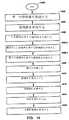
従って、単一の帯域の無線通信アンテナを周波数調整するための方法が提供される。本
方法は、放射体を形成するステップと、放射体に隣接する強誘電体材料を有する誘電体を
形成するステップと、電圧を強誘電体材料に印加するステップと、電圧の印加に応答して
誘電率を発生させるステップと、誘電率に応答して共振周波数で電磁場に伝達するステッ
プとを包含する。本方法のいくつかの局面は、印加された電圧を変化させるステップと、
印加された電圧の変化に応答して共振周波数を修正するステップとをさらに包含する。Accordingly, a method for frequency tuning a single band wireless communication antenna is provided. The method includes forming a radiator, forming a dielectric having a ferroelectric material adjacent to the radiator, applying a voltage to the ferroelectric material, and in response to applying the voltage. Generating a dielectric constant and transmitting the dielectric constant to the electromagnetic field at a resonant frequency in response to the dielectric constant. Some aspects of the method include changing the applied voltage;
Modifying the resonant frequency in response to changes in the applied voltage.
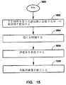
共振周波数を修正するステップは、印加された電圧に応答する種々の動作周波数を用い
てアンテナを形成するステップを包含する。代替的に説明されたように、種々の動作周波
数を用いてアンテナを形成するステップは、共振周波数に依存しない所定の固定された特
性インピーダンスを用いてアンテナを形成するステップを包含する。Modifying the resonant frequency includes forming the antenna with various operating frequencies that are responsive to the applied voltage. As alternatively described, forming the antenna using various operating frequencies includes forming the antenna using a predetermined fixed characteristic impedance that is independent of the resonant frequency.
本方法のいくつかの局面では、放射体を形成するステップは、単一の放射体を形成する
ステップである。In some aspects of the method, forming the radiator is forming a single radiator.
本方法のいくつかの局面では、強誘電体材料を有する誘電体を形成するステップは、固
定された誘電率を有する第1の材料から強誘電体材料を有する誘電体を形成するステップ
と、種々の誘電率を有する強誘電体材料を有する誘電体を形成するステップを含む。次い
で、共振周波数を修正するステップは、強誘電体材料の誘電率の変更に応答して共振周波
数を修正するステップを包含する。In some aspects of the method, forming a dielectric having a ferroelectric material includes forming a dielectric having a ferroelectric material from a first material having a fixed dielectric constant; Forming a dielectric having a ferroelectric material having a dielectric constant of: Then, modifying the resonant frequency includes modifying the resonant frequency in response to a change in the dielectric constant of the ferroelectric material.
他の局面では、強誘電体材料を有する誘電体を形成するステップは、複数の誘電体材料
を有する誘電体を形成するステップを包含し、誘電体材料の各々は、固定された誘電率を
有する材料を形成する。あるいはまたはさらに、強誘電体材料を用いて誘電体を形成する
ステップは、複数の強誘電体材料を有する誘電体を形成するステップを包含し、各強誘電
体材料は、種々の誘電率を有する。In another aspect, forming a dielectric having a ferroelectric material includes forming a dielectric having a plurality of dielectric materials, each of the dielectric materials having a fixed dielectric constant. Form material. Alternatively or additionally, forming a dielectric using a ferroelectric material includes forming a dielectric having a plurality of ferroelectric materials, each ferroelectric material having a different dielectric constant. .
上記方法のさらなる詳細およびFE材料の誘電体を用いて製造されたアンテナの群は、
以下に説明される。Further details of the above method and a group of antennas manufactured using a dielectric of FE material are:
This will be described below.
(好適な実施形態の詳細な説明)
本発明は、選択可能な動作周波数を有するアンテナの群を説明する。一般的には、各ア
ンテナは、種々の誘電率を有する放射体に近接する強誘電体材料を有する放射体および誘
電体を含む。放射体は、強誘電体材料の誘電率に応答する周波数で共振する。いくつかの
アンテナは、放射体に対して接地部を含む。他のアンテナ設計は、任意に設計された接地
武および放射体を含む。さらなる他の設計は、互いに明瞭に区別できない接地部および放
射体を含む。(Detailed description of preferred embodiments)
The present invention describes a group of antennas having selectable operating frequencies. In general, each antenna includes a radiator and a dielectric having a ferroelectric material proximate to the radiator having various dielectric constants. The radiator resonates at a frequency that is responsive to the dielectric constant of the ferroelectric material. Some antennas include a ground for the radiator. Other antenna designs include arbitrarily designed ground and radiators. Still other designs include ground and radiators that are not clearly distinguishable from each other.
本発明の一局面では、以下に提示されたアンテナの群は、任意の明らかな帯域幅または
共振周波数変化を達成するための複数の放射体に依存する従来のアンテナとは異なり、単
一の放射体アンテナの共振周波数を効率的に調整するように含まれたFE誘電体層を有す
る。本発明は、そのアンテナの各々が、単一の放射体に対応する共振の1つの基本周波数
(基本周波数の高調波の考慮を除く)を有する点において単一の帯域として本明細書中で
定義される。アンテナの群の本発明の別の局面では、FE誘電体は、放射体と接地部(垂
直接地部)との間の最高密度の電磁場の領域に配置される。その結果、FE材料の誘電率
の変化は、アンテナの共振周波数の著しい変化を生成する。In one aspect of the present invention, the group of antennas presented below differs from conventional antennas that rely on multiple radiators to achieve any apparent bandwidth or resonant frequency change, An FE dielectric layer included to efficiently adjust the resonant frequency of the body antenna. The present invention is defined herein as a single band in that each of its antennas has one fundamental frequency of resonance (excluding consideration of harmonics of the fundamental frequency) corresponding to a single radiator. Is done. In another aspect of the invention of the group of antennas, the FE dielectric is placed in the region of the highest density electromagnetic field between the radiator and ground (vertical ground). As a result, the change in dielectric constant of the FE material produces a significant change in the resonant frequency of the antenna.
図1a〜図1cは、選択可能な動作周波数を有する本発明のパッチアンテナの図である
。図1aは、半波長の放射体の寸法を有し得る単一帯域のパッチアンテナの概略図である
。パッチアンテナ100は、接地部102および接地部の上にある強誘電体材料を有する
強誘電体104を含む。この誘電体は、強誘電体材料に印加された電圧に応答する種々の
誘電率を有する。少なくとも1つの放射体106は、誘電率に応答する共振周波数を有す
る誘電体104の上にある。パッチアンテナ100のいくつかの局面では、誘電体104
は、全体的にFE材料からなる層である。パッチアンテナの原理および設計は、当業者に
よって十分に理解され、簡略化の点で本明細書では繰り返されない。FE材料の使用は、
パッチアンテナに広範囲の選択可能な動作周波数を与えるが、設計の一般的な原理は、本
発明のFE材料によって変更されない。同軸供給線108は、放射体106に接続された
中心導電体110を有し、接地部102に接続されたグランドを有する。1a-1c are diagrams of the patch antenna of the present invention having selectable operating frequencies. FIG. 1a is a schematic diagram of a single band patch antenna that may have the dimensions of a half-wave radiator.
Is a layer made entirely of FE material. The principles and design of patch antennas are well understood by those skilled in the art and are not repeated here for simplicity. Use of FE material
Although providing the patch antenna with a wide range of selectable operating frequencies, the general principles of design are not altered by the FE material of the present invention. The
図1bは、図1aのパッチアンテナ100の平面図である。典型的には、FE材料を有
する誘電体は、放射体106の近傍に配置されるだけである。領域112は、固定された
定数を有する誘電体であり得る。示されない代替の実施形態では、FE誘電体104は、
放電体106を全ての面上で取り囲んでもよいし、誘電体領域104および112が放射
体106の周りに対称的に形成されてもよい。FIG. 1b is a plan view of the
The
図1cは、1/4波長の放射体の寸法を有するのに適切であり得るような逆F状平面ア
ンテナの断面図である。FE誘電体104は、単一の放射体106と接地部102との間
に配置されたFE誘電体104が示されるが、他のFE誘電体パターンおよび分布もまた
実用的である。FIG. 1c is a cross-sectional view of an inverted F-shaped planar antenna that may be suitable to have a 1/4 wavelength radiator dimension. The FE dielectric 104 is shown as an FE dielectric 104 disposed between a
アンテナ100は、共振周波数に依存しない所定の固定された特性を有する。すなわち
、例えば、入力インピーダンスは、選択された動作周波数であるにもかかわらず、例えば
50オームのままである。あるいは、アンテナ100は、共振周波数に依存しない所定の
ほぼ一定のゲインを有すると説明することができる。The
図2は、図1aのパッチアンテナの代替的な局面を示す断面図である。示されたように
、誘電体104は、固定された誘電率を有する誘電体200に隣接する、固定された誘電
率を有する第1の材料から形成された誘電体層200および可変誘電率を有する強誘電体
材料から形成された誘電体202の内の少なくとも1つを含む。示されたように、FE材
料202を有する誘電体は、固定された誘電率を有する誘電体200の上にある。典型的
には、電圧は、所望の誘電率を生成するためにFE誘電体層202の近傍の導電体に印加
される。「+」および「−」符号によって表された電圧は、電圧発生器203によって供
給され得る。いくつかの局面では、電気絶縁体(図示されない)は、ac信号電圧からバ
イアス電圧を絶縁するために、層202と導電放射体106との間に配置され得る。しか
し、導電体のシートは、通常、アンテナ調整を妨害するFE誘電体202上にバイアス電
圧を均一に分散することが必要とされる。従って、dc電圧は、典型的には、放射体によ
って導かれたac信号上に重ね合わせられ、基準グランドは、接地部102に供給される
。あるいは、示されないが、固定された誘電率で形成された誘電体200は、強誘電体材
料202を有する誘電体の上にある。再度、絶縁体は、FE誘電体層202と導電性接地
部との間に配置され得、接地部における電圧とは異なる供給された基準電圧が供給される
。しかし、示されたように、FE誘電体層は、典型的には、接地部に供給された基準電圧
にバイアスされる。アンテナのいくつかの局面において、バイアス電圧極性は、示された
極性から反転されることに留意すること。FIG. 2 is a cross-sectional view illustrating an alternative aspect of the patch antenna of FIG. 1a. As shown, the dielectric 104 has a
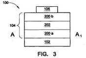
図3は、複数の固定された誘電率層を有する図1aのパッチアンテナの代替的な局面を
示す断面図である。固定された誘電率を有する誘電体は、固定された誘電率を有する誘電
体202の下にある第1の層200a、および強誘電体材料202を有する誘電体の上に
ある第2の層200bを形成する。2つの固定された誘電体層は、必ずしも同じ誘電率を
有する必要はない。さらに、固定された誘電体の3つ以上の層の使用もまた可能である。
あるいは、示されないが、複数のFE層が固定された誘電体の層の周辺で形成されてもよ
いし、固定された誘電体およびFE層の両方の複数の層が使用されてもよい。複数のFE
誘電体層は、異なるFE材料から作製され異なる厚さを有してもよいし、他の場合では、
同じ電圧に関して異なる誘電率を有する。FIG. 3 is a cross-sectional view illustrating an alternative aspect of the patch antenna of FIG. 1a having a plurality of fixed dielectric constant layers. A dielectric having a fixed dielectric constant includes a first layer 200a underlying the dielectric 202 having a fixed dielectric constant and a second layer 200b above the dielectric having a
Alternatively, although not shown, multiple FE layers may be formed around a fixed dielectric layer, or multiple layers of both fixed dielectric and FE layers may be used. Multiple FE
The dielectric layers may be made from different FE materials and have different thicknesses, in other cases,
Have different dielectric constants for the same voltage.
図4は、FE材料の内部層を有する図1aのパッチアンテナの代替の局面を示す断面図
である。示されたように、強誘電体材料を有する誘電体202は、固定された誘電率を有
する誘電体200の内部に形成される。あるいは、示されないが、固定された誘電率を有
する誘電体は、FE誘電体202の内部に形成される。さらに、複数の内部FE誘電体領
域が使用され得る。FIG. 4 is a cross-sectional view illustrating an alternate aspect of the patch antenna of FIG. 1a having an inner layer of FE material. As shown, a dielectric 202 having a ferroelectric material is formed inside a dielectric 200 having a fixed dielectric constant. Alternatively, although not shown, a dielectric having a fixed dielectric constant is formed inside the
いくつかの局面では、強誘電体材料を有する誘電体202は、バリウムストロンチウム
チタネートBaxSr1−xTiO3(BSTO)から形成される。しかし、代替のFE
材料は、周知であり、等価に実行され得る。図2に戻ると、例えば、強誘電体材料を有す
る誘電体202は、0.15〜2ミクロンの範囲の厚さ206を有する薄膜層で形成され
得る。あるいは、強誘電体材料を有する誘電体202は、1.5〜1000ミクロンの範
囲の厚さを有する厚膜206で形成される。いくつかの局面では、強誘電体材料を有する
誘電体は、0ボルトにおいて100〜5000の範囲の誘電率を有する。他の局面では、
固定された誘電率を有する第1の材料200から形成された誘電体および強誘電体材料2
02から形成された誘電体は、0ボルトにおいて2〜100の範囲の複合誘電率を有する
。In some aspects, the dielectric 202 having a ferroelectric material is formed from barium strontium titanate Bax Sr1-x TiO3 (BSTO). But alternative FE
The materials are well known and can be implemented equivalently. Returning to FIG. 2, for example, the dielectric 202 having a ferroelectric material may be formed of a thin film layer having a
Dielectric and ferroelectric material 2 formed from a
The dielectric formed from 02 has a composite dielectric constant in the range of 2-100 at 0 volts.
FE材料の誘電率は、ドーピングおよびキューリー温度(Tc)の制御によって操作さ
れ得る。いくつかの一般的なドーパント材料は、酸化物として導入された、タングステン
(W)、マンガン(Mn)、およびマグネシウム(Mg)である。しかし、周期表の同じ
列の他の等価な元素もまた実用的であり得る。FE材料は、いずれかの方向における温度
の変化によって急速な誘電降下(dielectric falling)を有するTc
において最大誘電率を有する。しかし、典型的にはTcより高い温度の誘電率のわずかな
変化がある。従って、FE材料のTcは、典型的には、誘電材料によって観測される動作
温度未満であるように選択される。The dielectric constant of the FE material can be manipulated by controlling the doping and Curie temperature (Tc). Some common dopant materials are tungsten (W), manganese (Mn), and magnesium (Mg), introduced as oxides. However, other equivalent elements in the same column of the periodic table may also be practical. FE materials have a Tc that has a rapid dielectric fall due to temperature changes in either direction.
Has a maximum dielectric constant. However, there is typically a slight change in dielectric constant at temperatures above Tc. Thus, the Tc of the FE material is typically selected to be below the operating temperature observed by the dielectric material.
誘電率1(空気)を用いて構成されたアンテナは、より高い誘電率材料を用いて構成さ
れたアンテナよりも小さい損失を有する。しかし、より高い誘電率材料は、しばしば、ア
ンテナの大きさ(有効波長)を低減する際に有用である。一般的に、アンテナ設計者は、
100未満の誘電率を有する誘電材料を探求する。FE材料の誘電率は、可変性を犠牲に
してドーパントを加えることによって低減され得る(バイアスボルト当たりの誘電率の変
化は少ない)。Tcとドーピングとの間の適切なトレードオフは、バイアス電圧のボルト
変化未満のFE材料における2:1変化よりも大きい変化を実用的にし得る。An antenna configured with a dielectric constant of 1 (air) has a lower loss than an antenna configured with a higher dielectric constant material. However, higher dielectric constant materials are often useful in reducing antenna size (effective wavelength). In general, antenna designers
Search for dielectric materials having a dielectric constant of less than 100. The dielectric constant of the FE material can be reduced by adding a dopant at the expense of variability (less change in dielectric constant per bias volt). A suitable trade-off between Tc and doping can make a change greater than a 2: 1 change in FE material less than a volt change in bias voltage.
図5a〜図9eは、本発明のスロットアンテナの群を示す。一般的には、各単一帯域幅
のスロットアンテナは、接地部および接地部の上にある強誘電体材料を有する誘電体を含
む。しかし、いくつかのスロットは、単に放射体を有するか、または仮想放射体または仮
想接地部を有するものとして理解され得る。接地部または放射体のいずれかにおいて形成
されたスロットは、誘電率に応答する電気的長さを有し、そして誘電率は、強誘電体材料
に印加された電圧に応答して誘電率変化を有する。放射体は、誘電体の上にあり、誘電体
に隣接する。Figures 5a to 9e show a group of slot antennas of the present invention. In general, each single bandwidth slot antenna includes a dielectric having a ground portion and a ferroelectric material overlying the ground portion. However, some slots may be understood as simply having a radiator or having a virtual radiator or virtual ground. Slots formed in either the ground or the radiator have an electrical length that is responsive to the dielectric constant, and the dielectric constant changes the dielectric constant in response to a voltage applied to the ferroelectric material. Have. The radiator is above the dielectric and is adjacent to the dielectric.
スロット設計の各々における放射体が共振周波数に依存しない所定の固定された特性イ
ンピーダンスを有することもまた一般的に真実である。すなわち、1つ以上のスロットの
電気的長さは、共振周波数に対して一定である。あるいは、レーダは、共振周波数に依存
しない所定のほぼ一定のゲインを有する。1つ以上のスロットが誘電体に対して共振周波
数の約半波長かまたは誘電体に対して共振周波数の約1/4波長のいずれかである1つ以
上の誘電率に応答して変化する電気的長さを有することが一般的に真実である。スロット
アンテナの原理および設計は、当業者によって十分理解され、そして簡略化の目的ため本
明細書中で繰り返されない。FE材料の使用はスロットアンテナに選択可能な動作周波数
のより広い範囲を与えるが、設計の一般的原理は、本発明のFE材料によって変更されな
い。It is also generally true that the radiator in each of the slot designs has a predetermined fixed characteristic impedance that is independent of the resonant frequency. That is, the electrical length of one or more slots is constant with respect to the resonance frequency. Alternatively, the radar has a predetermined substantially constant gain that does not depend on the resonant frequency. Electricity in which one or more slots change in response to one or more dielectric constants that are either about half a wavelength of the resonant frequency for the dielectric or about a quarter wavelength of the resonant frequency for the dielectric. It is generally true to have a reasonable length. The principles and design of slot antennas are well understood by those skilled in the art and are not repeated here for the sake of simplicity. Although the use of FE material gives the slot antenna a wider range of selectable operating frequencies, the general principles of design are not altered by the FE material of the present invention.
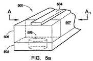
図5aは、本発明のマイクロストリップスロットアンテナ500の概略図である。接地
部502、放射体504、および強誘電体材料506を有する誘電体は、マイクロストリ
ップを形成する。典型的には、強誘電体材料を有する誘電体506は、示されるようにス
ロット近接して配置される。スロットから離れた異なる誘電体507(固定された誘電率
を有する)が使用され得る。スロット508は、接地部502において形成される。示さ
れたように、スロット508は放射体504を横切るが、必ずしもスロット508は放射
体504を横切る必要はない。マイクロストリップスロット500の他の局面では、複数
のスロット(図示されない)が使用される。FIG. 5a is a schematic diagram of a
図5bは、図5aのマイクロストリップアンテナの代替の局面を示す断面図である。示
されたように、誘電体506は、固定された誘電率を有する第1の材料から形成された誘
電体層510および固定された誘電率を有する誘電体510に隣接する種々の誘電率を有
する強誘電体材料から形成された誘電体512の内の少なくとも1つを含む。示されたよ
うに、FE材料を有する誘電体512は、固定された誘電率510を有する誘電体の上に
ある。典型的には、電圧は、所望された誘電率を生成するためにFE誘電体層512に近
接する導電体に印加される。「+」および「−」の符号によって示された電圧が供給され
得る。いくつかの局面では、電気絶縁体(図示せず)が層512と導電放射体504との
間に挿入され得、ac信号電圧からバイアス電圧を絶縁する。しかし、通常導電体のシー
トは、アンテナ調整を妨害するFE誘電体512上にバイアス電圧を均一に分布させるこ
とが必要とされる。従って、通常dc電圧は、放射体によって導かれたac信号上に重ね
合わせられ、そして基準グランドは、接地部502に供給される。あるいは、示されない
が、固定された誘電率によって形成された誘電体510は、強誘電体材料を有する誘電体
512の上にある。再度、絶縁体は、FE誘電体層512と導電性接地部との間に配置さ
れ得、接地部における電圧とは異なる基準グラウンドが供給される。しかし、示されたよ
うに、FE誘電体層は、典型的には接地部に供給された基準グランドによってバイアスさ
れる。アンテナのいくつかの局面では、バイアス電圧極性が示された極性から反転される
ことに留意すること。FIG. 5b is a cross-sectional view illustrating an alternative aspect of the microstrip antenna of FIG. 5a. As shown, dielectric 506 has various dielectric constants adjacent to
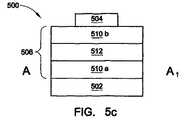
図5cは、複数の固定された誘電率層を有する図5aのマイクロストリップスロットア
ンテナの代替的な局面を示す断面図である。固定された誘電体を有する誘電体は、固定さ
れた誘電率を有する誘電体512の下にある第1の層510a、および強誘電体材料を有
する誘電体512の上にある2の層510bを形成する。2つの固定された誘電体層は、
必ずしも同じ誘電率または厚さを有する必要はない。さらに、3つ以上の固定された誘電
体層が使用され得る。あるいは、示されないが、複数のFE層が固定された誘電体層に近
接して形成されてもよいし、固定された誘電体およびFE層の両方の複数の層が使用され
得る。異なるFE材料から作製された複数のFE誘電体層が異なる厚さを有してもよいし
、あるいは他の場合では、同じ電圧に対して異なる誘電率を有してもよい。FIG. 5c is a cross-sectional view illustrating an alternative aspect of the microstrip slot antenna of FIG. 5a having a plurality of fixed dielectric layers. A dielectric having a fixed dielectric comprises a first layer 510a underlying the dielectric 512 having a fixed dielectric constant, and a second layer 510b above the dielectric 512 having a ferroelectric material. Form. The two fixed dielectric layers are
It is not necessary to have the same dielectric constant or thickness. In addition, more than two fixed dielectric layers can be used. Alternatively, although not shown, multiple FE layers may be formed proximate to the fixed dielectric layer, and multiple layers of both fixed dielectric and FE layers may be used. Multiple FE dielectric layers made from different FE materials may have different thicknesses, or in other cases may have different dielectric constants for the same voltage.
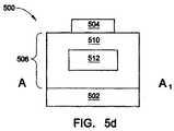
図5dは、FE材料の内部層を有する図5aのマイクロストリップスロットアンテナの
代替的な局面を示す断面図である。示されたように、強誘電体材料を有する誘電体512
は、固定された誘電率を有する誘電体510の内部に形成される。いくつかの局面では、
複数のFE内部領域が形成され得る。あるいは、示されないが、固定された誘電率を有す
る誘電体510は、FE誘電体512の内部に形成される。再度、さらなる電気絶縁体が
、接地部502から絶縁され、そして放射体504がFE層512から絶縁されるために
使用され得る。FIG. 5d is a cross-sectional view illustrating an alternative aspect of the microstrip slot antenna of FIG. 5a having an inner layer of FE material. As shown, a dielectric 512 having a ferroelectric material.
Are formed inside a dielectric 510 having a fixed dielectric constant. In some aspects,
Multiple FE internal regions may be formed. Alternatively, although not shown, a dielectric 510 having a fixed dielectric constant is formed inside the
いくつかの局面では、強誘電体材料を有する誘電体512がバリウムストロンチウムチ
タネートBaxSr1−xTiO3(BSTO)から形成される。しかし、代替のFE材
料は、周知であり、等価に実行され得る。図5bに戻ると、例えば、強誘電体材料を有す
る誘電体512は、0.15〜2ミクロンの範囲の厚さ514を有する薄膜層で形成され
得る。あるいは、強誘電体材料を有する誘電体512は、1.5〜1000ミクロンの範
囲の厚さを有する厚膜514で形成される。いくつかの局面では、強誘電体材料を有する
誘電体は、0ボルトにおいて100〜5000の範囲の誘電率を有する。他の局面では、
固定された誘電率を有する第1の材料から形成された誘電体および強誘電体材料から形成
された誘電体は、0ボルトにおいて2〜100の範囲の複合誘電率を有する。In some aspects, a dielectric 512 having a ferroelectric material is formed from barium strontium titanate Bax Sr1-x TiO3 (BSTO). However, alternative FE materials are well known and can be implemented equivalently. Returning to FIG. 5b, for example, a dielectric 512 having a ferroelectric material may be formed of a thin film layer having a
A dielectric formed from a first material having a fixed dielectric constant and a dielectric formed from a ferroelectric material has a composite dielectric constant in the range of 2-100 at 0 volts.
FE材料の誘電率は、キューリー温度(Tc)のドーピングおよび制御を介して操作さ
れ得る。いくつかの一般的なドーパント材料は、酸化物として導入された、タングステン
(W)、マンガン(Mn)、およびマグネシウム(Mg)である。しかし、周期表の同じ
列の他の等価な元素もまた実用的であり得る。FE材料は、いずれかの方向における温度
の変化によって急速な誘電降下を有するTcにおいて最大誘電率を有する。しかし、典型
的にはTcより高い温度の誘電率のわずかな変化がある。従って、FE材料のTcは、典
型的には、誘電材料によって観測される動作温度未満であるように選択される。The dielectric constant of the FE material can be manipulated through Curie temperature (Tc) doping and control. Some common dopant materials are tungsten (W), manganese (Mn), and magnesium (Mg), introduced as oxides. However, other equivalent elements in the same column of the periodic table may also be practical. The FE material has a maximum dielectric constant at Tc that has a rapid dielectric drop due to temperature changes in either direction. However, there is typically a slight change in dielectric constant at temperatures above Tc. Thus, the Tc of the FE material is typically selected to be below the operating temperature observed by the dielectric material.
誘電率1(空気)を用いて構成されたアンテナは、より高い誘電率材料を用いて構成さ
れたアンテナよりも小さい損失を有する。しかし、より高い誘電率材料は、しばしば、ア
ンテナの大きさ(有効波長)を低減する際に有用である。一般的に、アンテナ設計者は、
100未満の誘電率を有する誘電材料を探求する。FE材料の誘電率は、可変性を犠牲に
してドーパントを加えることによって低減され得る(バイアスボルト当たりの誘電率の変
化は少ない)。Tcとドーピングとの間の適切なトレードオフは、バイアス電圧のボルト
変化未満のFE材料における2:1変化よりも大きい変化を実用的にし得る。An antenna configured with a dielectric constant of 1 (air) has a lower loss than an antenna configured with a higher dielectric constant material. However, higher dielectric constant materials are often useful in reducing antenna size (effective wavelength). In general, antenna designers
Search for dielectric materials having a dielectric constant of less than 100. The dielectric constant of the FE material can be reduced by adding a dopant at the expense of variability (less change in dielectric constant per bias volt). A suitable trade-off between Tc and doping can make a change greater than a 2: 1 change in FE material less than a volt change in bias voltage.
図6aは、本発明の同軸スロットアンテナ600の概略図である。接地部602、放射
体604、FE材料を有する誘電体606は、接地部602においてスロット608を有
する同軸線を形成する。FE誘電体606は、スロット608に近接している。スロット
から離れた固定された誘電率を有する異なる誘電体607が使用され得る。示されたよう
に、スロット608は放射体604を横切るが、必ずしもスロット608は放射体604
を横切る必要はない。同軸スロットアンテナ600の他の局面では、複数のスロット(図
示されない)が使用される。FIG. 6a is a schematic diagram of a
There is no need to cross. In other aspects of the
図6bは、図6aの同軸スロットアンテナの代替の局面を示す断面図である。示される
ように、誘電体606は、固定された誘電率を有する第1の材料から形成された誘電体層
610および固定された誘電率を有する誘電体610に隣接する種々の誘電率を有する強
誘電体材料から形成された誘電体612の内の少なくとも1つを含む。示されたように、
FE材料を有する誘電体612は、固定された誘電率610を有する誘電体の上にある。
典型的には、電圧は、所望された誘電率を生成するためにFE誘電体層612に近接する
導電体に印加される。「+」および「−」の符号によって示された電圧が供給され得る。
いくつかの局面では、電気絶縁体(図示せず)が層612と導電放射体604との間に挿
入され得、ac信号電圧からバイアス電圧を絶縁する。しかし、通常導電体のシートは、
アンテナ調整を妨害するFE誘電体612上にバイアス電圧を均一に分布させることが必
要とされる。従って、通常dc電圧は、放射体によって導かれたac信号上に重ね合わせ
られ、そして基準グランドは、接地部602に供給される。あるいは、示されないが、固
定された誘電率によって形成された誘電体610は、強誘電体材料を有する誘電体612
の上にある。再度、絶縁体は、FE誘電体層612と導電性接地部との間に配置され得、
接地部における電圧とは異なる基準グラウンドが供給される。しかし、示されたように、
FE誘電体層は、典型的には接地部に供給された基準グランドによってバイアスされる。
アンテナのいくつかの局面では、バイアス電圧極性が示された極性から反転されることに
留意すること。6b is a cross-sectional view illustrating an alternative aspect of the coaxial slot antenna of FIG. 6a. As shown, dielectric 606 includes a
A dielectric 612 with FE material is on top of a dielectric with a fixed
Typically, a voltage is applied to a conductor proximate to the
In some aspects, an electrical insulator (not shown) can be inserted between
A uniform distribution of the bias voltage on the FE dielectric 612 that interferes with antenna tuning is required. Thus, the normal dc voltage is superimposed on the ac signal derived by the radiator and the reference ground is provided to the
Is on the top. Again, the insulator can be placed between the
A reference ground different from the voltage at the ground is supplied. But as shown,
The FE dielectric layer is typically biased by a reference ground supplied to the ground.
Note that in some aspects of the antenna, the bias voltage polarity is reversed from the indicated polarity.
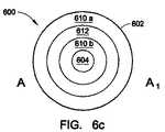
図6cは、複数の固定された誘電率層を有する図6aの同軸スロットアンテナの代替的
な局面を示す断面図である。固定された誘電体を有する誘電体は、固定された誘電率を有
する誘電体612の下にある第1の層610a、および強誘電体材料を有する誘電体61
2の上にある第2の層610bを形成する。2つの固定された誘電体層は、必ずしも同じ
誘電率または厚さを有する必要はない。さらに、3つ以上の固定された誘電体層が使用さ
れ得る。あるいは、示されないが、複数のFE層が固定された誘電体層近接して形成され
てもよいし、固定された誘電体およびFE層の両方の複数の層が使用されてもよい。異な
るFE材料から作製された複数のFE誘電体層が異なる厚さを有してもよいし、あるいは
他の場合では、同じ電圧に対して異なる誘電率を有してもよい。6c is a cross-sectional view illustrating an alternate aspect of the coaxial slot antenna of FIG. 6a having a plurality of fixed dielectric layers. A dielectric having a fixed dielectric includes a first layer 610a underlying a dielectric 612 having a fixed dielectric constant, and a dielectric 61 having a ferroelectric material.
A second layer 610b overlying 2 is formed. The two fixed dielectric layers need not have the same dielectric constant or thickness. In addition, more than two fixed dielectric layers can be used. Alternatively, although not shown, multiple FE layers may be formed proximate to the fixed dielectric layer, or multiple layers of both fixed dielectric and FE layers may be used. Multiple FE dielectric layers made from different FE materials may have different thicknesses, or in other cases may have different dielectric constants for the same voltage.
図6dは、FE材料の内部層を有する図6aの同軸スロットアンテナの代替的な局面を
示す断面図である。示されたように、強誘電体材料を有する誘電体612は、固定された
誘電率を有する誘電体610の内部に形成される。複数の内部領域が形成され得るが、1
つのみの内部領域が示されることに留意すること。あるいは、示されないが、固定された
誘電率を有する誘電体610は、FE誘電体612の内部に形成される。再度、さらなる
電気絶縁体が、接地部602から絶縁され、そして放射体604がFE層612から絶縁
されるために使用される。FIG. 6d is a cross-sectional view illustrating an alternative aspect of the coaxial slot antenna of FIG. 6a having an inner layer of FE material. As shown, a dielectric 612 having a ferroelectric material is formed inside a dielectric 610 having a fixed dielectric constant. Multiple internal regions can be formed, but 1
Note that only one internal area is shown. Alternatively, although not shown, a dielectric 610 having a fixed dielectric constant is formed inside the
いくつかの局面では、強誘電体材料を有する誘電体612がバリウムストロンチウムチ
タネートBaxSr1−xTiO3(BSTO)から形成される。しかし、代替のFE材
料は、周知であり、等価に実行され得る。図6bに戻ると、例えば、強誘電体材料を有す
る誘電体612は、0.15〜2ミクロンの範囲の厚さ614を有する薄膜層で形成され
得る。あるいは、強誘電体材料を有する誘電体612は、1.5〜1000ミクロンの範
囲の厚さを有する厚膜614で形成される。いくつかの局面では、強誘電体材料を有する
誘電体は、0ボルトにおいて100〜5000の範囲の誘電率を有する。他の局面では、
固定された誘電率を有する第1の材料から形成された誘電体および強誘電体材料から形成
された誘電体は、0ボルトにおいて2〜100の範囲の複合誘電率を有する。In some aspects, a dielectric 612 having a ferroelectric material is formed from barium strontium titanate Bax Sr1-x TiO3 (BSTO). However, alternative FE materials are well known and can be implemented equivalently. Returning to FIG. 6b, for example, a dielectric 612 having a ferroelectric material may be formed of a thin film layer having a
A dielectric formed from a first material having a fixed dielectric constant and a dielectric formed from a ferroelectric material has a composite dielectric constant in the range of 2-100 at 0 volts.
FE材料の誘電率は、キューリー温度(Tc)のドーピングおよび制御を介して操作さ
れ得る。いくつかの一般的なドーパント材料は、酸化物として導入された、タングステン
(W)、マンガン(Mn)、およびマグネシウム(Mg)である。しかし、周期表の同じ
列の他の等価な元素もまた実用的であり得る。FE材料は、いずれかの方向における温度
の変化によって急速な誘電降下を有するTcにおいて最大誘電率を有する。しかし、典型
的にはTcより高い温度の誘電率のわずかな変化がある。従って、FE材料のTcは、典
型的には、誘電材料によって観測される動作温度未満であるように選択される。The dielectric constant of the FE material can be manipulated through Curie temperature (Tc) doping and control. Some common dopant materials are tungsten (W), manganese (Mn), and magnesium (Mg), introduced as oxides. However, other equivalent elements in the same column of the periodic table may also be practical. The FE material has a maximum dielectric constant at Tc that has a rapid dielectric drop due to temperature changes in either direction. However, there is typically a slight change in dielectric constant at temperatures above Tc. Thus, the Tc of the FE material is typically selected to be below the operating temperature observed by the dielectric material.
誘電率1(空気)を用いて構成されたアンテナは、より高い誘電率材料を用いて構成さ
れたアンテナよりも小さい損失を有する。しかし、より高い誘電率材料は、しばしば、ア
ンテナの大きさ(有効波長)を低減する際に有用である。一般的に、アンテナ設計者は、
100未満の誘電率を有する誘電材料を探求する。FE材料の誘電率は、可変性を犠牲に
してドーパントを加えることによって低減され得る(バイアスボルト当たりの誘電率の変
化は少ない)。Tcとドーピングとの間の適切なトレードオフは、バイアス電圧のボルト
変化未満のFE材料における2:1変化よりも大きい変化を実用的にし得る。An antenna configured with a dielectric constant of 1 (air) has a lower loss than an antenna configured with a higher dielectric constant material. However, higher dielectric constant materials are often useful in reducing antenna size (effective wavelength). In general, antenna designers
Search for dielectric materials having a dielectric constant of less than 100. The dielectric constant of the FE material can be reduced by adding a dopant at the expense of variability (less change in dielectric constant per bias volt). A suitable trade-off between Tc and doping can make a change greater than a 2: 1 change in FE material less than a volt change in bias voltage.
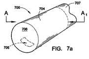
図7a〜図7fは、本発明の円形導波管スロットアンテナ700の図である。周知であ
るように、図7aでは、接地部および放射体は、明確に区別できず、従って円形導波管ア
ンテナは、放射体704および誘電体706を含むものとして説明される。示されたよう
にスロット708は放射体704を横切るが、必ずしもスロット708は放射体704を
横切る必要はない。FE誘電体706は、スロット708近接して配置される。他の場合
では、固定された誘電材料707がスロット708と離れて使用され得る。円形導波管ス
ロットアンテナ700の他の局面では、複数のスロット(図示されない)が使用される。7a-7f are diagrams of a circular
図7bは、図7aの円形導波管スロットアンテナの代替の局面を示す断面図である。示
されるように、誘電体706は、固定された誘電率を有する第1の材料から形成された誘
電体層710および固定された誘電率を有する誘電体710に隣接する種々の誘電率を有
する強誘電体材料から形成された誘電体712の内の少なくとも1つを含む。示されたよ
うに、FE材料を有する誘電体712は、固定された誘電率710を有する誘電体の上に
ある。典型的には、電圧は、所望された誘電率を生成するためにFE誘電体層712に近
接する導電体に印加される。「+」および「−」の符号によって示された電圧が供給され
得る。いくつかの局面では、電気絶縁体(図示せず)が層712と導電放射体704との
間に挿入され得、ac信号電圧からバイアス電圧を絶縁する。しかし、通常導電体のシー
トは、アンテナ調整を妨害するFE誘電体712上にバイアス電圧を均一に分布させるこ
とが必要とされる。従って、スリット709は、2つのバイアス電圧極性を分離するため
に放射体704に形成され得る。通常dc電圧は、半分の放射体(radiator h
alves)によって導かれたac信号上に重ね合わせられる。あるいは、示されないが
、固定された誘電率によって形成された誘電体710は、強誘電体材料を有する誘電体7
12の上にある。アンテナのいくつかの局面では、バイアス電圧極性が示された極性から
反転されることに留意すること。FIG. 7b is a cross-sectional view illustrating an alternate aspect of the circular waveguide slot antenna of FIG. 7a. As shown, dielectric 706 includes a
superimposed on the ac signal derived by (alves). Alternatively, although not shown, the dielectric 710 formed by a fixed dielectric constant is a dielectric 7 having a ferroelectric material.
12 above. Note that in some aspects of the antenna, the bias voltage polarity is reversed from the indicated polarity.
図7cは、複数の固定された誘電率層を有する図7aの円形導波管スロットアンテナの
代替的な局面を示す断面図である。固定された誘電体を有する誘電体は、固定された誘電
率を有する誘電体712の下にある第1の層710a、および強誘電体材料を有する誘電
体712の上にある第2の層710bを形成する。2つの固定された誘電体層は、必ずし
も同じ誘電率または厚さを有する必要はない。さらに、3つ以上の固定された誘電体層が
使用され得る。あるいは、示されないが、複数のFE層が固定された誘電体層近接して形
成されてもよいし、固定された誘電体およびFE層の両方の複数の層が使用されてもよい
。異なるFE材料から作製された複数のFE誘電体層が異なる厚さを有してもよいし、あ
るいは他の場合では、同じ電圧に対して異なる誘電率を有してもよい。FIG. 7c is a cross-sectional view illustrating an alternative aspect of the circular waveguide slot antenna of FIG. 7a having a plurality of fixed dielectric layers. A dielectric having a fixed dielectric is composed of a first layer 710a underlying the dielectric 712 having a fixed dielectric constant and a
図7dは、FE材料の内部層を有する図7aの円形導波管スロットアンテナの代替的な
局面を示す断面図である。示されたように、強誘電体材料を有する誘電体712は、固定
された誘電率を有する誘電体710の内部に形成される。複数の内部領域が形成され得る
が、1つのみの内部領域が示されることに留意すること。いくつかの局面では、複数のF
E内部領域が形成され得る。あるいは、示されないが、固定された誘電率を有する誘電体
710は、FE誘電体712の内部に形成される。内部領域が矩形形状として示されるが
、円形、円筒、および楕円形状等の他の形状が同様に実用的であることに留意されるべき
である。FIG. 7d is a cross-sectional view illustrating an alternative aspect of the circular waveguide slot antenna of FIG. 7a with an inner layer of FE material. As shown, a dielectric 712 having a ferroelectric material is formed inside a dielectric 710 having a fixed dielectric constant. Note that multiple internal regions may be formed, but only one internal region is shown. In some aspects, multiple Fs
An E internal region may be formed. Alternatively, although not shown, a dielectric 710 having a fixed dielectric constant is formed inside the
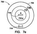
図7eおよび図7fは、円形導波管スロットアンテナ700の代替の局面である。この
スリットは必ずしも必要ではない。なぜなら放射体704は、バイアス電圧を運ぶ必要が
ないためである。その代わりに、バイアス電圧がパネル714および716によって供給
される。このバイアスパネル714/716は、FE誘電体の一方の側状の種々の位置で
配置され得る。1つのパネルは、スロット内で均一に配置され得る。FIGS. 7 e and 7 f are alternative aspects of the circular
いくつかの局面では、強誘電体材料を有する誘電体712がバリウムストロンチウムチ
タネートBaxSr1−xTiO3(BSTO)から形成される。しかし、代替のFE材
料は、周知であり、等価に実行され得る。図7bに戻ると、例えば、強誘電体材料を有す
る誘電体712は、0.15〜2ミクロンの範囲の厚さ714を有する薄膜層で形成され
得る。あるいは、強誘電体材料を有する誘電体712は、1.5〜1000ミクロンの範
囲の厚さを有する厚膜714で形成される。いくつかの局面では、強誘電体材料を有する
誘電体は、0ボルトにおいて100〜5000の範囲の誘電率を有する。他の局面では、
固定された誘電率を有する第1の材料から形成された誘電体および強誘電体材料から形成
された誘電体は、0ボルトにおいて2〜100の範囲の複合誘電率を有する。In some aspects, a dielectric 712 having a ferroelectric material is formed from barium strontium titanate Bax Sr1-x TiO3 (BSTO). However, alternative FE materials are well known and can be implemented equivalently. Returning to FIG. 7b, for example, a dielectric 712 having a ferroelectric material may be formed of a thin film layer having a
A dielectric formed from a first material having a fixed dielectric constant and a dielectric formed from a ferroelectric material has a composite dielectric constant in the range of 2-100 at 0 volts.
FE材料の誘電率は、キューリー温度(Tc)のドーピングおよび制御を介して操作さ
れ得る。いくつかの一般的なドーパント材料は、酸化物として導入された、タングステン
(W)、マンガン(Mn)、およびマグネシウム(Mg)である。しかし、周期表の同じ
列の他の等価な元素もまた実用的であり得る。FE材料は、いずれかの方向における温度
の変化によって急速な誘電降下を有するTcにおいて最大誘電率を有する。しかし、典型
的にはTcより高い温度の誘電率のわずかな変化がある。従って、FE材料のTcは、典
型的には、誘電材料によって観測される動作温度未満であるように選択される。The dielectric constant of the FE material can be manipulated through Curie temperature (Tc) doping and control. Some common dopant materials are tungsten (W), manganese (Mn), and magnesium (Mg), introduced as oxides. However, other equivalent elements in the same column of the periodic table may also be practical. The FE material has a maximum dielectric constant at Tc that has a rapid dielectric drop due to temperature changes in either direction. However, there is typically a slight change in dielectric constant at temperatures above Tc. Thus, the Tc of the FE material is typically selected to be below the operating temperature observed by the dielectric material.
誘電率1(空気)を用いて構成されたアンテナは、より高い誘電率材料を用いて構成さ
れたアンテナよりも小さい損失を有する。しかし、より高い誘電率材料は、しばしば、ア
ンテナの大きさ(有効波長)を低減する際に有用である。一般的に、アンテナ設計者は、
100未満の誘電率を有する誘電材料を探求する。FE材料の誘電率は、可変性を犠牲に
してドーパントを加えることによって低減され得る(バイアスボルト当たりの誘電率の変
化は少ない)。Tcとドーピングとの間の適切なトレードオフは、バイアス電圧のボルト
変化未満のFE材料における2:1変化よりも大きい変化を実用的にし得る。An antenna configured with a dielectric constant of 1 (air) has a lower loss than an antenna configured with a higher dielectric constant material. However, higher dielectric constant materials are often useful in reducing antenna size (effective wavelength). In general, antenna designers
Search for dielectric materials having a dielectric constant of less than 100. The dielectric constant of the FE material can be reduced by adding a dopant at the expense of variability (less change in dielectric constant per bias volt). A suitable trade-off between Tc and doping can make a change greater than a 2: 1 change in FE material less than a volt change in bias voltage.
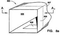
図8aは、本発明の矩形導波管アンテナ800の概略図である。矩形導波管アンテナは
、放射体804および誘電体806を含むものとして説明される。しかし、放射体および
接地部の指定が任意である。示されたように、スロット808は放射体804を横切るが
、必ずしもスロット808は放射体704を横切る必要はない。FE誘電体806は、ス
ロット808近接して配置される。他の場合では、固定された誘電材料807がスロット
808と離れて使用され得る。矩形導波管スロットアンテナ800の他の局面では、複数
のスロット(図示されない)が使用される。FIG. 8a is a schematic diagram of a
図8bは、図8aの矩形導波管スロットアンテナの代替の局面を示す断面図である。示
されるように、誘電体806は、固定された誘電率を有する第1の材料から形成された誘
電体層810および固定された誘電率を有する誘電体810に隣接する種々の誘電率を有
する強誘電体材料から形成された誘電体812の内の少なくとも1つを含む。示されたよ
うに、FE材料を有する誘電体812は、固定された誘電率810を有する誘電体の上に
ある。典型的には、電圧は、所望された誘電率を生成するためにFE誘電体層812に近
接する導電体に印加される。「+」および「−」の符号によって示された電圧が供給され
得る。いくつかの局面では、電気絶縁体(図示せず)が層812と導電放射体804との
間に挿入され得、ac信号電圧からバイアス電圧を絶縁する。しかし、通常導電体のシー
トは、アンテナ調整を妨害するFE誘電体812上にバイアス電圧を均一に分布させるこ
とが必要とされる。従って、スリット809(電気的に絶縁している)は、2つのバイア
ス電圧極性を分離するために放射体804に形成され得る。典型的にはdc電圧は、半分
の放射体によって導かれたac信号上に重ね合わせられる。あるいは、示されないが、固
定された誘電率によって形成された誘電体810は、強誘電体材料を有する誘電体812
の上にある。アンテナのいくつかの局面では、バイアス電圧極性が示された極性から反転
されることに留意すること。FIG. 8b is a cross-sectional view illustrating an alternate aspect of the rectangular waveguide slot antenna of FIG. 8a. As shown, dielectric 806 includes a
Is on the top. Note that in some aspects of the antenna, the bias voltage polarity is reversed from the indicated polarity.
図8cは、複数の固定された誘電率層を有する図8aの矩形導波管スロットアンテナの
代替的な局面を示す断面図である。固定された誘電体を有する誘電体は、固定された誘電
率を有する誘電体812の下にある第1の層810a、および強誘電体材料を有する誘電
体812の上にある第2の層810bを形成する。2つの固定された誘電体層は、必ずし
も同じ誘電率または厚さを有する必要はない。さらに、3つ以上の固定された誘電体層が
使用され得る。あるいは、示されないが、複数のFE層が固定された誘電体層近接して形
成されてもよいし、固定された誘電体およびFE層の両方の複数の層が使用されてもよい
。異なるFE材料から作製された複数のFE誘電体層が異なる厚さを有してもよいし、あ
るいは他の場合では、同じ電圧に対して異なる誘電率を有してもよい。FIG. 8c is a cross-sectional view illustrating an alternative aspect of the rectangular waveguide slot antenna of FIG. 8a having a plurality of fixed dielectric layers. A dielectric having a fixed dielectric is composed of a first layer 810a underlying the dielectric 812 having a fixed dielectric constant and a second layer 810b above the dielectric 812 having a ferroelectric material. Form. The two fixed dielectric layers need not have the same dielectric constant or thickness. In addition, more than two fixed dielectric layers can be used. Alternatively, although not shown, multiple FE layers may be formed proximate to the fixed dielectric layer, or multiple layers of both fixed dielectric and FE layers may be used. Multiple FE dielectric layers made from different FE materials may have different thicknesses, or in other cases may have different dielectric constants for the same voltage.
図8dは、FE材料の内部層を有する図8aの矩形導波管スロットアンテナの代替的な
局面を示す断面図である。示されたように、強誘電体材料を有する誘電体812は、固定
された誘電率を有する誘電体810の内部に形成される。複数の内部領域が形成され得る
が、1つのみの内部領域が示されることに留意すること。あるいは、示されないが、固定
された誘電率を有する誘電体810は、FE誘電体812の内部に形成される。内部領域
が矩形形状として示されるが、円形、円筒、および楕円形状等の他の形状が同様に実用的
であることに留意されるべきである。図7eおよび図7fに等しい示されない別のバージ
ョンでは、dcバイアス電圧が放射体804の内部のパネルによって供給され、その結果
スリット809が形成される必要がない。FIG. 8d is a cross-sectional view illustrating an alternative aspect of the rectangular waveguide slot antenna of FIG. 8a with an inner layer of FE material. As shown, a dielectric 812 having a ferroelectric material is formed inside a dielectric 810 having a fixed dielectric constant. Note that multiple internal regions may be formed, but only one internal region is shown. Alternatively, although not shown, a dielectric 810 having a fixed dielectric constant is formed inside the
いくつかの局面では、強誘電体材料を有する誘電体812がバリウムストロンチウムチ
タネートBaxSr1−xTiO3(BSTO)から形成される。しかし、代替のFE材
料は、周知であり、等価に実行され得る。図8bに戻ると、例えば、強誘電体材料を有す
る誘電体812は、0.15〜2ミクロンの範囲の厚さ814を有する薄膜層で形成され
得る。あるいは、強誘電体材料を有する誘電体812は、1.5〜1000ミクロンの範
囲の厚さを有する厚膜814で形成される。いくつかの局面では、強誘電体材料を有する
誘電体は、0ボルトにおいて100〜5000の範囲の誘電率を有する。他の局面では、
固定された誘電率を有する第1の材料から形成された誘電体および強誘電体材料から形成
された誘電体は、0ボルトにおいて2〜100の範囲の複合誘電率を有する。In some aspects, a dielectric 812 having a ferroelectric material is formed from barium strontium titanate Bax Sr1-x TiO3 (BSTO). However, alternative FE materials are well known and can be implemented equivalently. Returning to FIG. 8b, for example, a dielectric 812 having a ferroelectric material may be formed of a thin film layer having a
A dielectric formed from a first material having a fixed dielectric constant and a dielectric formed from a ferroelectric material has a composite dielectric constant in the range of 2-100 at 0 volts.
FE材料の誘電率は、キューリー温度(Tc)のドーピングおよび制御を介して操作さ
れ得る。いくつかの一般的なドーパント材料は、酸化物として導入された、タングステン
(W)、マンガン(Mn)、およびマグネシウム(Mg)である。しかし、周期表の同じ
列の他の等価な元素もまた実用的であり得る。FE材料は、いずれかの方向における温度
の変化によって急速な誘電降下を有するTcにおいて最大誘電率を有する。しかし、典型
的にはTcより高い温度の誘電率のわずかな変化がある。従って、FE材料のTcは、典
型的には、誘電材料によって観測される動作温度未満であるように選択される。The dielectric constant of the FE material can be manipulated through Curie temperature (Tc) doping and control. Some common dopant materials are tungsten (W), manganese (Mn), and magnesium (Mg), introduced as oxides. However, other equivalent elements in the same column of the periodic table may also be practical. The FE material has a maximum dielectric constant at Tc that has a rapid dielectric drop due to temperature changes in either direction. However, there is typically a slight change in dielectric constant at temperatures above Tc. Thus, the Tc of the FE material is typically selected to be below the operating temperature observed by the dielectric material.
誘電率1(空気)を用いて構成されたアンテナは、より高い誘電率材料を用いて構成さ
れたアンテナよりも小さい損失を有する。しかし、より高い誘電率材料は、しばしば、ア
ンテナの大きさ(有効波長)を低減する際に有用である。一般的に、アンテナ設計者は、
100未満の誘電率を有する誘電材料を探求する。FE材料の誘電率は、可変性を犠牲に
してドーパントを加えることによって低減され得る(バイアスボルト当たりの誘電率の変
化は少ない)。Tcとドーピングとの間の適切なトレードオフは、バイアス電圧のボルト
変化未満のFE材料における2:1変化よりも大きい変化を実用的にし得る。An antenna configured with a dielectric constant of 1 (air) has a lower loss than an antenna configured with a higher dielectric constant material. However, higher dielectric constant materials are often useful in reducing antenna size (effective wavelength). In general, antenna designers
Search for dielectric materials having a dielectric constant of less than 100. The dielectric constant of the FE material can be reduced by adding a dopant at the expense of variability (less change in dielectric constant per bias volt). A suitable trade-off between Tc and doping can make a change greater than a 2: 1 change in FE material less than a volt change in bias voltage.
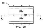
図9aおよび図9bは、それぞれ本発明のフレアノッチアンテナの部分断面図および平
面図である。フレアノッチアンテナ900は、接地部902、放射体904、および誘電
体906aおよび906aを含み、それらの内の少なくとも1つはFE材料を含む。接地
部および放射体の指定は任意であると考えられ得る。スロットまたはノッチ907が示さ
れる。FE誘電体906aおよび906bは、ノッチ907に隣接して配置される。ある
いは、中心導電体908およびグランド909を有する供給部(feed)が示される。9a and 9b are a partial cross-sectional view and a plan view, respectively, of the flare notch antenna of the present invention. Flared
図9cは、図9bのフレアノッチアンテナの代替的な局面を示す断面図である。示され
たように、誘電体906aおよび906bは、固定された誘電率を有する第1の材料から
形成された誘電体層910および固定された誘電率を有する誘電体910に隣接する種々
の誘電率を有する強誘電体材料から形成された誘電体912の内の少なくとも1つを含む
。示されたように、FE材料を有する誘電体912は、固定された誘電率910を有する
誘電体の上にある。典型的には、電圧は、所望された誘電率を生成するためにFE誘電体
層912に近接する導電体に印加される。「+」および「−」の符号によって示された電
圧が供給され得る。いくつかの局面では、電気絶縁体(図示せず)が層912と放射体/
接地部904/902との間に挿入され得、ac信号電圧からバイアス電圧を絶縁する。
しかし、通常導電体のシートは、アンテナ調整を妨害するFE誘電体912上にバイアス
電圧を均一に分布させることが必要とされる。従って、dc電圧は、典型的には、放射体
/接地部904/902によって導かれたac信号上に重ね合わせられ、そして基準グラ
ンドは、導電パネル914に供給される。あるいは、示されないが、固定された誘電率に
よって形成された誘電体910は、強誘電体材料を有する誘電体912の上にある。アン
テナのいくつかの局面では、バイアス電圧極性が示された極性から反転されることに留意
すること。FIG. 9c is a cross-sectional view illustrating an alternative aspect of the flare notch antenna of FIG. 9b. As shown,
It can be inserted between the
However, normally a sheet of conductor is required to distribute the bias voltage evenly over the FE dielectric 912 that interferes with antenna tuning. Thus, the dc voltage is typically superimposed on the ac signal derived by the radiator /
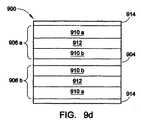
図9dは、複数の固定された誘電率層を有する図9bのフレアノッチアンテナの代替的
な局面を示す断面図である。固定された誘電体を有する誘電体は、固定された誘電率を有
する誘電体912の下にある第1の層910a、および強誘電体材料を有する誘電体91
2の上にある第2の層910bを形成する。2つの固定された誘電体層は、必ずしも同じ
誘電率または厚さを有する必要はない。さらに、3つ以上の固定された誘電体層が使用さ
れてもよい。あるいは、示されないが、複数のFE層が固定された誘電体層近接して形成
されてもよいし、固定された誘電体およびFE層の両方の複数の層が使用されてもよい。
異なるFE材料から作製された複数のFE誘電体層が異なる厚さを有してもよいし、ある
いは他の場合では、同じ電圧に対して異なる誘電率を有してもよい。FIG. 9d is a cross-sectional view illustrating an alternative aspect of the flare notch antenna of FIG. 9b having a plurality of fixed dielectric layers. A dielectric having a fixed dielectric includes a first layer 910a underlying a dielectric 912 having a fixed dielectric constant, and a dielectric 91 having a ferroelectric material.
A second layer 910b overlying 2 is formed. The two fixed dielectric layers need not have the same dielectric constant or thickness. In addition, more than two fixed dielectric layers may be used. Alternatively, although not shown, multiple FE layers may be formed proximate to the fixed dielectric layer, or multiple layers of both fixed dielectric and FE layers may be used.
Multiple FE dielectric layers made from different FE materials may have different thicknesses, or in other cases may have different dielectric constants for the same voltage.
図9eは、FE材料の内部層を有する図9bのフレアノッチマイクアンテナの代替的な
局面を示す平面図である。示されたように、強誘電体材料を有する誘電体912は、固定
された誘電率を有する誘電体910の内部に形成される。複数の内部領域が形成され得る
が、1つのみが示される。あるいは、示されないが、固定された誘電率を有する誘電体9
10は、FE誘電体912の内部に形成される。内部領域が矩形形状として示されるが、
円形、円筒、および楕円形状等の他の形状が同様に実用的であることに留意されるべきで
ある。示されない別のバージョンでは、FE材料は、放射体の1つのみの面上に内部領域
を形成する(例えば、誘電体906a)。FIG. 9e is a plan view illustrating an alternative aspect of the flare notch microphone antenna of FIG. 9b with an inner layer of FE material. As shown, a dielectric 912 having a ferroelectric material is formed inside a dielectric 910 having a fixed dielectric constant. Multiple internal regions may be formed, but only one is shown. Alternatively, although not shown, a dielectric 9 having a fixed dielectric constant
10 is formed inside the
It should be noted that other shapes such as circular, cylindrical, and elliptical shapes are equally practical. In another version not shown, the FE material forms an internal region on only one face of the radiator (eg, dielectric 906a).
いくつかの局面では、強誘電体材料を有する誘電体912がバリウムストロンチウムチ
タネートBaxSr1−xTiO3(BSTO)から形成される。しかし、代替のFE材
料は、周知であり、等価に実行され得る。図9cに戻ると、例えば、強誘電体材料を有す
る誘電体912は、0.15〜2ミクロンの範囲の厚さ914を有する薄膜層で形成され
得る。あるいは、強誘電体材料を有する誘電体912は、1.5〜1000ミクロンの範
囲の厚さを有する厚膜914で形成される。いくつかの局面では、強誘電体材料を有する
誘電体は、0ボルトにおいて100〜5000の範囲の誘電率を有する。他の局面では、
固定された誘電率を有する第1の材料から形成された誘電体および強誘電体材料から形成
された誘電体は、0ボルトにおいて2〜100の範囲の複合誘電率を有する。In some aspects, a dielectric 912 having a ferroelectric material is formed from barium strontium titanate Bax Sr1-x TiO3 (BSTO). However, alternative FE materials are well known and can be implemented equivalently. Returning to FIG. 9c, for example, a dielectric 912 having a ferroelectric material may be formed of a thin film layer having a
A dielectric formed from a first material having a fixed dielectric constant and a dielectric formed from a ferroelectric material has a composite dielectric constant in the range of 2-100 at 0 volts.
FE材料の誘電率は、キューリー温度(Tc)のドーピングおよび制御を介して操作さ
れ得る。いくつかの一般的なドーパント材料は、酸化物として導入された、タングステン
(W)、マンガン(Mn)、およびマグネシウム(Mg)である。しかし、周期表の同じ
列の他の等価な元素もまた実用的であり得る。FE材料は、いずれかの方向における温度
の変化によって急速な誘電降下を有するTcにおいて最大誘電率を有する。しかし、典型
的にはTcより高い温度の誘電率のわずかな変化がある。従って、FE材料のTcは、典
型的には、誘電材料によって観測される動作温度未満であるように選択される。The dielectric constant of the FE material can be manipulated through Curie temperature (Tc) doping and control. Some common dopant materials are tungsten (W), manganese (Mn), and magnesium (Mg), introduced as oxides. However, other equivalent elements in the same column of the periodic table may also be practical. The FE material has a maximum dielectric constant at Tc that has a rapid dielectric drop due to temperature changes in either direction. However, there is typically a slight change in dielectric constant at temperatures above Tc. Thus, the Tc of the FE material is typically selected to be below the operating temperature observed by the dielectric material.
誘電率1(空気)を用いて構成されたアンテナは、より高い誘電率材料を用いて構成さ
れたアンテナよりも小さい損失を有する。しかし、より高い誘電率材料は、しばしば、ア
ンテナの大きさ(有効波長)を低減する際に有用である。一般的に、アンテナ設計者は、
100未満の誘電率を有する誘電材料を探求する。FE材料の誘電率は、可変性を犠牲に
してドーパントを加えることによって低減され得る(バイアスボルト当たりの誘電率の変
化は少ない)。Tcとドーピングとの間の適切なトレードオフは、バイアス電圧のボルト
変化未満のFE材料における2:1変化よりも大きい変化を実用的にし得る。An antenna configured with a dielectric constant of 1 (air) has a lower loss than an antenna configured with a higher dielectric constant material. However, higher dielectric constant materials are often useful in reducing antenna size (effective wavelength). In general, antenna designers
Search for dielectric materials having a dielectric constant of less than 100. The dielectric constant of the FE material can be reduced by adding a dopant at the expense of variability (less change in dielectric constant per bias volt). A suitable trade-off between Tc and doping can make a change greater than a 2: 1 change in FE material less than a volt change in bias voltage.
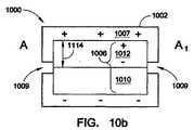
図10a〜図10dは、本発明の開口端導波管アンテナ1000の図である。図10a
は、選択された動作周波数を有する本発明の開口端導波管アンテナの部分断面図である。
開口端導波管アンテナ1000は、放射体1002に近接して配置された強誘電体材料を
有する放射体1002および誘電体1006を含む。誘電体1006は、強誘電体材料に
印加された電圧に応答する種々の誘電率を有する。接地部および放射体の指定は任意であ
る。典型的には、開口端1007が接地される。開口端107から離れた一定の誘電材料
1005が使用され得る。開口端アンテナの原理および設計は、当業者によって十分に理
解され、簡略化を意図して本明細書中で繰り返されない。FE材料の使用は、開口端アン
テナに選択可能な動作周波数のより広い範囲を提供し、設計の一般的な原理は、本発明の
FE材料によって変更されない。10a to 10d are views of the open
FIG. 4 is a partial cross-sectional view of the open-ended waveguide antenna of the present invention having a selected operating frequency.
Open
アンテナ1000は、共振周波数に依存しない所定の固定された特性インピーダンスを
有する。代替的に説明されたように、アンテナ1000は、共振周波数に依存しない所定
のほぼ一定のゲインを有する。The
図10bは、図10aの開口端導波管スロットアンテナの代替の局面を示す断面図であ
る。示されるように、誘電体1006は、固定された誘電率を有する第1の材料から形成
された誘電体層1010および固定された誘電率を有する誘電体1010に隣接する種々
の誘電率を有する強誘電体材料から形成された誘電体1012の内の少なくとも1つを含
む。示されたように、FE材料を有する誘電体1012は、固定された誘電率1010を
有する誘電体の上にある。典型的には、電圧は、所望された誘電率を生成するためにFE
誘電体層1012に近接する導電体に印加される。「+」および「−」の符号によって示
された電圧が供給され得る。いくつかの局面では、電気絶縁体(図示せず)が層1012
と導電放射体1004との間に挿入され得、ac信号電圧からバイアス電圧を絶縁する。
しかし、通常導電体のシートは、アンテナ調整を妨害するFE誘電体1012上にバイア
ス電圧を均一に分布させることが必要とされる。従って、電気的に絶縁しているスリット
1009は、2つのバイアス電圧極性を分離するために放射体1002に形成され得る。
通常dc電圧は、半分の放射体によって導かれたac信号上に重ね合わせられる。あるい
は、示されないが、固定された誘電率によって形成された誘電体1010は、強誘電体材
料を有する誘電体1012の上にある。アンテナのいくつかの局面では、バイアス電圧極
性が示された極性から反転されることに留意すること。10b is a cross-sectional view illustrating an alternative aspect of the open-ended waveguide slot antenna of FIG. 10a. As shown, dielectric 1006 includes a
Applied to a conductor proximate to
And the conductive radiator 1004 to insulate the bias voltage from the ac signal voltage.
However, usually a sheet of conductor is required to distribute the bias voltage evenly over the FE dielectric 1012 that interferes with antenna tuning. Accordingly, an electrically insulating
Usually the dc voltage is superimposed on the ac signal derived by half the radiator. Alternatively, although not shown, a dielectric 1010 formed with a fixed dielectric constant is on top of a dielectric 1012 having a ferroelectric material. Note that in some aspects of the antenna, the bias voltage polarity is reversed from the indicated polarity.
図10cは、複数の固定された誘電率層を有する図10aの開口端導波管スロットアン
テナの代替的な局面を示す断面図である。固定された誘電体を有する誘電体は、固定され
た誘電率を有する誘電体1012の下にある第1の層1010a、および強誘電体材料を
有する誘電体1012の上にある第2の層1010b。2つの固定された誘電体層は、必
ずしも同じ誘電率または厚さを有する必要はない。さらに、3つ以上の固定された誘電体
層が使用され得る。あるいは、示されないが、複数のFE層が固定された誘電体層近接し
て形成されてもよいし、固定された誘電体およびFE層の両方の複数の層が使用されても
よい。異なるFE材料から作製された複数のFE誘電体層が異なる厚さを有してもよいし
、あるいは他の場合では、同じ電圧に対して異なる誘電率を有してもよい。10c is a cross-sectional view illustrating an alternative aspect of the open-ended waveguide slot antenna of FIG. 10a having a plurality of fixed dielectric constant layers. A dielectric having a fixed dielectric is a first layer 1010a underlying the dielectric 1012 having a fixed dielectric constant and a second layer 1010b above the dielectric 1012 having a ferroelectric material. . The two fixed dielectric layers need not have the same dielectric constant or thickness. In addition, more than two fixed dielectric layers can be used. Alternatively, although not shown, multiple FE layers may be formed proximate to the fixed dielectric layer, or multiple layers of both fixed dielectric and FE layers may be used. Multiple FE dielectric layers made from different FE materials may have different thicknesses, or in other cases may have different dielectric constants for the same voltage.
図10dは、FE材料の内部層を有する図10aの開口端導波管スロットアンテナの代
替的な局面を示す平面図である。示されたように、強誘電体材料を有する誘電体1012
は、固定された誘電率を有する誘電体1010の内部に形成される。複数の内部領域が形
成され得るが、1つのみが示される。あるいは、示されないが、固定された誘電率を有す
る誘電体1010は、FE誘電体1012の内部に形成される。内部領域が矩形形状とし
て示されるが、円形、円筒、および楕円形状等の他の形状が同様に実用的であることに留
意されるべきである。図7eおよび図7fに等しい示されない別のバージョンでは、dc
バイアス電圧が放射体1002の内部のパネルによって供給され、その結果スリット10
09が形成される必要がない。FIG. 10d is a plan view illustrating an alternative aspect of the open-ended waveguide slot antenna of FIG. 10a with an inner layer of FE material. As shown, dielectric 1012 with a ferroelectric material.
Are formed inside a dielectric 1010 having a fixed dielectric constant. Multiple internal regions may be formed, but only one is shown. Alternatively, although not shown, a dielectric 1010 having a fixed dielectric constant is formed inside the
A bias voltage is supplied by the panel inside the
09 need not be formed.
いくつかの局面では、強誘電体材料を有する誘電体1012がバリウムストロンチウム
チタネートBaxSr1−xTiO3(BSTO)から形成される。しかし、代替のFE
材料は、周知であり、等価に実行され得る。図10bに戻ると、例えば、強誘電体材料を
有する誘電体1012は、0.15〜2ミクロンの範囲の厚さ1014を有する薄膜層で
形成され得る。あるいは、強誘電体材料を有する誘電体1012は、1.5〜1000ミ
クロンの範囲の厚さを有する厚膜1014で形成される。いくつかの局面では、強誘電体
材料を有する誘電体は、0ボルトにおいて100〜5000の範囲の誘電率を有する。他
の局面では、固定された誘電率を有する第1の材料から形成された誘電体および強誘電体
材料から形成された誘電体は、0ボルトにおいて2〜100の範囲の複合誘電率を有する
。In some aspects, a dielectric 1012 having a ferroelectric material is formed from barium strontium titanate Bax Sr1-x TiO3 (BSTO). But alternative FE
The materials are well known and can be implemented equivalently. Returning to FIG. 10b, for example, a dielectric 1012 having a ferroelectric material may be formed of a thin film layer having a thickness 1014 in the range of 0.15 to 2 microns. Alternatively, the dielectric 1012 having a ferroelectric material is formed of a thick film 1014 having a thickness in the range of 1.5 to 1000 microns. In some aspects, the dielectric having a ferroelectric material has a dielectric constant in the range of 100-5000 at 0 volts. In other aspects, a dielectric formed from a first material having a fixed dielectric constant and a dielectric formed from a ferroelectric material has a composite dielectric constant in the range of 2-100 at 0 volts.
FE材料の誘電率は、キューリー温度(Tc)のドーピングおよび制御を介して操作さ
れ得る。いくつかの一般的なドーパント材料は、酸化物として導入された、タングステン
(W)、マンガン(Mn)、およびマグネシウム(Mg)である。しかし、周期表の同じ
列の他の等価な元素もまた実用的であり得る。FE材料は、いずれかの方向における温度
の変化によって急速な誘電降下を有するTcにおいて最大誘電率を有する。しかし、典型
的にはTcより高い温度の誘電率のわずかな変化がある。従って、FE材料のTcは、典
型的には、誘電材料によって観測される動作温度未満であるように選択される。The dielectric constant of the FE material can be manipulated through Curie temperature (Tc) doping and control. Some common dopant materials are tungsten (W), manganese (Mn), and magnesium (Mg), introduced as oxides. However, other equivalent elements in the same column of the periodic table may also be practical. The FE material has a maximum dielectric constant at Tc that has a rapid dielectric drop due to temperature changes in either direction. However, there is typically a slight change in dielectric constant at temperatures above Tc. Thus, the Tc of the FE material is typically selected to be below the operating temperature observed by the dielectric material.
誘電率1(空気)を用いて構成されたアンテナは、より高い誘電率材料を用いて構成さ
れたアンテナよりも小さい損失を有する。しかし、より高い誘電率材料は、しばしば、ア
ンテナの大きさ(有効波長)を低減する際に有用である。一般的に、アンテナ設計者は、
100未満の誘電率を有する誘電材料を探求する。FE材料の誘電率は、可変性を犠牲に
してドーパントを加えることによって低減され得る(バイアスボルト当たりの誘電率の変
化は少ない)。Tcとドーピングとの間の適切なトレードオフは、バイアス電圧のボルト
変化未満のFE材料における2:1変化よりも大きい変化を実用的にし得る。An antenna configured with a dielectric constant of 1 (air) has a lower loss than an antenna configured with a higher dielectric constant material. However, higher dielectric constant materials are often useful in reducing antenna size (effective wavelength). In general, antenna designers
Search for dielectric materials having a dielectric constant of less than 100. The dielectric constant of the FE material can be reduced by adding a dopant at the expense of variability (less change in dielectric constant per bias volt). A suitable trade-off between Tc and doping can make a change greater than a 2: 1 change in FE material less than a volt change in bias voltage.
図10a〜図10bを参照すると、開口端矩形導波管が示されてきたが、上記解析およ
び説明を開口端円形導波管および開口端プレートアンテナに適用する。さらに、開口端導
波管アンテナ1000が、同軸ケーブル、平行板、または任意の種類の導波管である選択
された信号供給を有し得る。Referring to FIGS. 10a-10b, open end rectangular waveguides have been shown, but the above analysis and description apply to open end circular waveguides and open end plate antennas. Further, the open-ended
図11a〜図11eは、選択可能な動作周波数を有する本発明ホーンアンテナの図であ
る。図11aに見られるように、ホーンアンテナ1100は、放射体ホーン1102およ
び放射体ホーンに隣接して配置された強誘電体材料を有する誘電体1106を含む。誘電
体1006は、強誘電体材料に印加された電圧に応答する種々の誘電率を有する。中央導
電体1005を有する同軸供給線1004が示される。ホーン1002は、誘電率に応答
する電気的長さ1109を有する。電気的長さは、共振周波数に応答する電気的長さ11
09を有する。ホーンは、接地されてもよいし、開いていてもよい。再度接地部および放
射体の指定が任意である。ホーンアンテナの原理および設計が当業者によって理解され、
簡便さのために本発明で繰り返されない。FE材料の使用は、ホーンアンテナに選択可能
な動作周波数の広い範囲を与えるが、設計の一般的な原理は、本発明のFE材料によって
変更されない。Figures 11a to 11e are diagrams of a horn antenna of the present invention having a selectable operating frequency. As seen in FIG. 11a, the
09. The horn may be grounded or open. The grounding part and the radiator can be specified again. The principle and design of the horn antenna is understood by those skilled in the art,
For simplicity, it will not be repeated in the present invention. Although the use of FE material gives the horn antenna a wide range of selectable operating frequencies, the general principles of design are not altered by the FE material of the present invention.
ホーンアンテナ1100は、共振周波数から独立して所定の固定された特性インピーダ
ンスを有する、あるいは、ホーンアンテナ1100は、共振周波数に依存しない所定のほ
ぼ一定の定数を有する。The
図11bは、図11aのホーンアンテナの代替の局面を示す断面図である。示されるよ
うに、誘電体1106は、固定された誘電率を有する第1の材料から形成された誘電体層
1110および固定された誘電率を有する誘電体1110に隣接する種々の誘電率を有す
る強誘電体材料から形成された誘電体1112の内の少なくとも1つを含む。示されたよ
うに、FE材料を有する誘電体1112は、固定された誘電率1110を有する誘電体の
上にある。典型的には、電圧は、所望された誘電率を生成するためにFE誘電体層111
2に近接する導電体に印加される。「+」および「−」の符号によって示された電圧が供
給され得る。いくつかの局面では、電気絶縁体(図示せず)が層1112と放射体ホーン
1102との間に挿入され得、ac信号電圧からバイアス電圧を絶縁する。しかし、通常
導電体のシートは、アンテナ調整を妨害するFE誘電体1112上にバイアス電圧を均一
に分布させることが必要とされる。従って、電気的に絶縁しているスリット1108は、
2つのバイアス電圧極性を分離するために放射体1102に形成され得る。通常dc電圧
は、半分の放射体によって導かれたac信号上に重ね合わせられる。あるいは、示されな
いが、固定された誘電率によって形成された誘電体1110は、強誘電体材料を有する誘
電体1112の上にある。アンテナのいくつかの局面では、バイアス電圧極性が示された
極性から反転されることに留意すること。FIG. 11b is a cross-sectional view illustrating an alternative aspect of the horn antenna of FIG. 11a. As shown, dielectric 1106 includes a
2 is applied to a conductor close to 2. The voltages indicated by the “+” and “−” signs may be supplied. In some aspects, an electrical insulator (not shown) may be inserted between
A
図11cおよび11dは、複数の固定された誘電率層を有する図11aのホーンアンテ
ナの代替的な局面を示す断面図である。固定された誘電体を有する誘電体は、固定された
誘電率を有する誘電体1112の下にある第1の層1110a、および強誘電体材料を有
する誘電体1112の上にある第2の層1110bを形成する。2つの固定された誘電体
層は、必ずしも同じ誘電率または厚さを有する必要はない。さらに、3つ以上の固定され
た誘電体層が使用され得る。あるいは、示されないが、複数のFE層が固定された誘電体
層近接して形成されてもよいし、固定された誘電体およびFE層の両方の複数の層が使用
されてもよい。異なるFE材料から作製された複数のFE誘電体層が異なる厚さを有して
もよいし、あるいは他の場合では、同じ電圧に対して異なる誘電率を有してもよい。FIGS. 11c and 11d are cross-sectional views illustrating alternative aspects of the horn antenna of FIG. 11a having a plurality of fixed dielectric constant layers. A dielectric having a fixed dielectric is a
図11eは、FE材料の内部層を有する図11aのホーンアンテナの代替的な局面を示
す断面図である。示されたように、強誘電体材料を有する誘電体1112は、固定された
誘電率を有する誘電体1110の内部に形成される。複数の内部領域が形成され得るが、
1つのみが示されることに留意すること。あるいは、示されないが、固定された誘電率を
有する誘電体1110は、FE誘電体1112の内部に形成される。内部領域が矩形形状
として示されるが、円形、円筒、および楕円形状等の他の形状が同様に実用的であること
に留意されるべきである。図7eおよび図7fに等しい示されない別のバージョンでは、
dcバイアス電圧が放射体1002の内部のパネルによって供給され、その結果スリット
1108が形成される必要がない。FIG. 11e is a cross-sectional view illustrating an alternative aspect of the horn antenna of FIG. 11a with an inner layer of FE material. As shown, a dielectric 1112 having a ferroelectric material is formed inside a dielectric 1110 having a fixed dielectric constant. Multiple internal regions can be formed,
Note that only one is shown. Alternatively, although not shown, a dielectric 1110 having a fixed dielectric constant is formed inside the
A dc bias voltage is supplied by the panel inside the
いくつかの局面では、強誘電体材料を有する誘電体1112がバリウムストロンチウム
チタネートBaxSr1−xTiO3(BSTO)から形成される。しかし、代替のFE
材料は、周知であり、等価に実行され得る。図11dに戻ると、例えば、強誘電体材料を
有する誘電体1112は、0.15〜2ミクロンの範囲の厚さ1114を有する薄膜層で
形成され得る。あるいは、強誘電体材料を有する誘電体1112は、1.5〜1000ミ
クロンの範囲の厚さを有する厚膜1114で形成される。いくつかの局面では、強誘電体
材料を有する誘電体は、0ボルトにおいて100〜5000の範囲の誘電率を有する。他
の局面では、固定された誘電率を有する第1の材料から形成された誘電体および強誘電体
材料から形成された誘電体は、0ボルトにおいて2〜100の範囲の複合誘電率を有する
。In some aspects, a dielectric 1112 having a ferroelectric material is formed from barium strontium titanate Bax Sr1-x TiO3 (BSTO). But alternative FE
The materials are well known and can be implemented equivalently. Returning to FIG. 11d, for example, the dielectric 1112 having a ferroelectric material may be formed of a thin film layer having a
FE材料の誘電率は、キューリー温度(Tc)のドーピングおよび制御を介して操作さ
れ得る。いくつかの一般的なドーパント材料は、酸化物として導入された、タングステン
(W)、マンガン(Mn)、およびマグネシウム(Mg)である。しかし、周期表の同じ
列の他の等価な元素もまた実用的であり得る。FE材料は、いずれかの方向における温度
の変化によって急速な誘電降下を有するTcにおいて最大誘電率を有する。しかし、典型
的にはTcより高い温度の誘電率のわずかな変化がある。従って、FE材料のTcは、典
型的には、誘電材料によって観測される動作温度未満であるように選択される。The dielectric constant of the FE material can be manipulated through Curie temperature (Tc) doping and control. Some common dopant materials are tungsten (W), manganese (Mn), and magnesium (Mg), introduced as oxides. However, other equivalent elements in the same column of the periodic table may also be practical. The FE material has a maximum dielectric constant at Tc that has a rapid dielectric drop due to temperature changes in either direction. However, there is typically a slight change in dielectric constant at temperatures above Tc. Thus, the Tc of the FE material is typically selected to be below the operating temperature observed by the dielectric material.
誘電率1(空気)を用いて構成されたアンテナは、より高い誘電率材料を用いて構成さ
れたアンテナよりも小さい損失を有する。しかし、より高い誘電率材料は、しばしば、ア
ンテナの大きさ(有効波長)を低減する際に有用である。一般的に、アンテナ設計者は、
100未満の誘電率を有する誘電材料を探求する。FE材料の誘電率は、可変性を犠牲に
してドーパントを加えることによって低減され得る(バイアスボルト当たりの誘電率の変
化は少ない)。Tcとドーピングとの間の適切なトレードオフは、バイアス電圧のボルト
変化未満のFE材料における2:1変化よりも大きい変化を実用的にし得る。An antenna configured with a dielectric constant of 1 (air) has a lower loss than an antenna configured with a higher dielectric constant material. However, higher dielectric constant materials are often useful in reducing antenna size (effective wavelength). In general, antenna designers
Search for dielectric materials having a dielectric constant of less than 100. The dielectric constant of the FE material can be reduced by adding a dopant at the expense of variability (less change in dielectric constant per bias volt). A suitable trade-off between Tc and doping can make a change greater than a 2: 1 change in FE material less than a volt change in bias voltage.
図11aを参照すると、同軸ケーブル、円形導波管、矩形導波管からの信号供給または
平行板信号供給を用いる平行板ホーンアンテナに上記説明を同様に適用する。Referring to FIG. 11a, the above description applies similarly to a parallel plate horn antenna using a coaxial cable, a circular waveguide, a signal supply from a rectangular waveguide or a parallel plate signal supply.
図12a〜図12fは、選択可能な動作周波数を有する本発明のモノポールアンテナの
描写を表す。図12では、モノポールアンテナ1200は、少なくとも部分的に放射体1
202を取り囲んでいる、放射体1202、接地部1204、および誘電体1206を含
む。誘電体は、強誘電体材料に印加された電圧に応答する種々の誘電率を有する。放射体
1202は、誘電率に応答する電気的長さ1208を有する。あるいは、示されないが、
放射体1202は、螺旋形状で形成され得る。モノポールアンテナの原理および設計が当
業者によって十分に理解され、簡略化の点で本明細書では繰り返されない。FE材料の使
用は、モノポールアンテナに広範囲の選択可能な周波数を与えるが、設計の一般的な原理
は、本発明のFE材料によって変更されない。Figures 12a to 12f represent a depiction of a monopole antenna of the present invention having a selectable operating frequency. In FIG. 12, the
Surrounding 202 includes a
The
アンテナ1200は、共振周波数に依存しない所定の固定された特性を有する。すなわ
ち、放射体の電気的な長さは、共振周波数に対して一定である、あるいは、アンテナ12
00は、共振周波数に依存しない所定のほぼ一定のゲインを有する。The
00 has a predetermined substantially constant gain that does not depend on the resonance frequency.
図12bは、図12aのモノポールアンテナの代替の局面を示す断面図である。示され
るように、誘電体1206は、固定された誘電率を有する第1の材料から形成された誘電
体層1210および固定された誘電率を有する誘電体1210に隣接する種々の誘電率を
有する強誘電体材料から形成された誘電体1212の内の少なくとも1つを含む。示され
たように、FE材料を有する誘電体1212は、固定された誘電率1210を有する誘電
体の上にある。典型的には、電圧は、所望された誘電率を生成するためにFE誘電体層1
212に近接する導電体に印加される。「+」および「−」の符号によって示された電圧
が供給され得る。いくつかの局面では、電気絶縁体(図示せず)が層1212と放射体1
202との間に挿入され得、ac信号電圧からバイアス電圧を絶縁する。しかし、通常導
電体のシートは、アンテナ調整を妨害するFE誘電体1212上にバイアス電圧を均一に
分布させることが必要とされる。従って、典型的にはdc電圧は、放射体1202によっ
て導かれたac信号上に重ね合わせられ、そして基準グランドが導電パネル1214に供
給される。アンテナのいくつかの局面では、バイアス電圧極性が反転される。他の局面で
は、放射体1202は、dcバイアスを運ばず、その代わりに、2つのバイアス極性は、
パネル1214によって運ばれる。12b is a cross-sectional view illustrating an alternative aspect of the monopole antenna of FIG. 12a. As shown, dielectric 1206 includes a
Applied to a conductor proximate to 212. The voltages indicated by the “+” and “−” signs may be supplied. In some aspects, an electrical insulator (not shown) is provided between
202 to insulate the bias voltage from the ac signal voltage. However, typically a sheet of conductor is required to distribute the bias voltage evenly over the FE dielectric 1212 that interferes with antenna tuning. Thus, typically the dc voltage is superimposed on the ac signal derived by
Carried by
図12cは、複数の固定された誘電率層を有する図12aのモノポールアンテナの代替
的な局面を示す図である。固定された誘電体を有する誘電体は、固定された誘電率を有す
る誘電体1212の下にある第1の層1210a、および強誘電体材料を有する誘電体1
212の上にある第2の層1210bを形成する。2つの固定された誘電体層は、必ずし
も同じ誘電率または厚さを有する必要はない。さらに、3つ以上の固定された誘電体層が
使用され得る。あるいは、示されないが、複数のFE層が固定された誘電体層近接して形
成されてもよいし、固定された誘電体およびFE層の両方の複数の層が使用されてもよい
。異なるFE材料から作製された複数のFE誘電体層が異なる厚さを有してもよいし、あ
るいは他の場合では、同じ電圧に対して異なる誘電率を有してもよい。FIG. 12c shows an alternative aspect of the monopole antenna of FIG. 12a having a plurality of fixed dielectric layers. A dielectric having a fixed dielectric includes a first layer 1210a underlying a dielectric 1212 having a fixed dielectric constant, and a dielectric 1 having a ferroelectric material.
A second layer 1210b overlying 212 is formed. The two fixed dielectric layers need not have the same dielectric constant or thickness. In addition, more than two fixed dielectric layers can be used. Alternatively, although not shown, multiple FE layers may be formed proximate to the fixed dielectric layer, or multiple layers of both fixed dielectric and FE layers may be used. Multiple FE dielectric layers made from different FE materials may have different thicknesses, or in other cases may have different dielectric constants for the same voltage.
図12dは、FE材料の内部層を有する図12aのモノポールアンテナの代替的な局面
を示す図である。示されたように、強誘電体材料を有する誘電体1212は、固定された
誘電率を有する誘電体1210の内部に形成される。複数の内部領域が形成され得るが、
1つのみが示されることに留意すること。あるいは、示されないが、固定された誘電率を
有する誘電体1210は、FE誘電体1212の内部に形成される。内部領域が矩形形状
として示されるが、円形、円筒、および楕円形状等の他の形状が同様に実用的であること
に留意されるべきである。FIG. 12d shows an alternative aspect of the monopole antenna of FIG. 12a with an inner layer of FE material. As shown, a dielectric 1212 having a ferroelectric material is formed inside a dielectric 1210 having a fixed dielectric constant. Multiple internal regions can be formed,
Note that only one is shown. Alternatively, although not shown, a dielectric 1210 having a fixed dielectric constant is formed inside the
図12eおよび図12fは、本発明のモノポールアンテナのいくつかの代替的な局面を
示す。Figures 12e and 12f illustrate some alternative aspects of the monopole antenna of the present invention.
いくつかの局面では、強誘電体材料を有する誘電体1212がバリウムストロンチウム
チタネートBaxSr1−xTiO3(BSTO)から形成される。しかし、代替のFE
材料は、周知であり、等価に実行され得る。図12bに戻ると、例えば、強誘電体材料を
有する誘電体1212は、0.15〜2ミクロンの範囲の厚さ1214を有する薄膜層で
形成され得る。あるいは、強誘電体材料を有する誘電体1212は、1.5〜1000ミ
クロンの範囲の厚さを有する厚膜1214で形成される。いくつかの局面では、強誘電体
材料を有する誘電体は、0ボルトにおいて100〜5000の範囲の誘電率を有する。他
の局面では、固定された誘電率を有する第1の材料から形成された誘電体および強誘電体
材料から形成された誘電体は、0ボルトにおいて2〜100の範囲の複合誘電率を有する
。In some aspects, a dielectric 1212 having a ferroelectric material is formed from barium strontium titanate Bax Sr1-x TiO3 (BSTO). But alternative FE
The materials are well known and can be implemented equivalently. Returning to FIG. 12b, for example, a dielectric 1212 comprising a ferroelectric material may be formed of a thin film layer having a
FE材料の誘電率は、キューリー温度(Tc)のドーピングおよび制御を介して操作さ
れ得る。いくつかの一般的なドーパント材料は、酸化物として導入された、タングステン
(W)、マンガン(Mn)、およびマグネシウム(Mg)である。しかし、周期表の同じ
列の他の等価な元素もまた実用的であり得る。FE材料は、いずれかの方向における温度
の変化によって急速な誘電降下を有するTcにおいて最大誘電率を有する。しかし、典型
的にはTcより高い温度の誘電率のわずかな変化がある。従って、FE材料のTcは、典
型的には、誘電材料によって観測される動作温度未満であるように選択される。The dielectric constant of the FE material can be manipulated through Curie temperature (Tc) doping and control. Some common dopant materials are tungsten (W), manganese (Mn), and magnesium (Mg), introduced as oxides. However, other equivalent elements in the same column of the periodic table may also be practical. The FE material has a maximum dielectric constant at Tc that has a rapid dielectric drop due to temperature changes in either direction. However, there is typically a slight change in dielectric constant at temperatures above Tc. Thus, the Tc of the FE material is typically selected to be below the operating temperature observed by the dielectric material.
誘電率1(空気)を用いて構成されたアンテナは、より高い誘電率材料を用いて構成さ
れたアンテナよりも小さい損失を有する。しかし、より高い誘電率材料は、しばしば、ア
ンテナの大きさ(有効波長)を低減する際に有用である。一般的に、アンテナ設計者は、
100未満の誘電率を有する誘電材料を探求する。FE材料の誘電率は、可変性を犠牲に
してドーパントを加えることによって低減され得る(バイアスボルト当たりの誘電率の変
化は少ない)。Tcとドーピングとの間の適切なトレードオフは、バイアス電圧のボルト
変化未満のFE材料における2:1変化よりも大きい変化を実用的にし得る。An antenna configured with a dielectric constant of 1 (air) has a lower loss than an antenna configured with a higher dielectric constant material. However, higher dielectric constant materials are often useful in reducing antenna size (effective wavelength). In general, antenna designers
Search for dielectric materials having a dielectric constant of less than 100. The dielectric constant of the FE material can be reduced by adding a dopant at the expense of variability (less change in dielectric constant per bias volt). A suitable trade-off between Tc and doping can make a change greater than a 2: 1 change in FE material less than a volt change in bias voltage.
図13a〜図13fは、選択可能な動作周波数を有する本発明のダイポールアンテナの
描写を表す。図13aでは、ダイポールアンテナ1300は、少なくとも部分的に放射体
1302を取り囲んでいる、放射体1302、接地部1304、および誘電体1306を
含む。誘電体1306は、強誘電体材料に印加された電圧に応答する種々の誘電率を有す
る強誘電体材料を含む。放射体および接地部は、種々の誘電率に応答する電気的長さ13
08を有する。あるいは、示されないが、放射体1302、接地部1304、またはその
両方が螺旋形状で形成され得る。ダイポールアンテナの原理および設計が当業者によって
十分に理解され、簡略化の点で本明細書では繰り返されない。FE材料の使用は、パッチ
アンテナに広範囲の選択可能な周波数を与えるが、設計の一般的な原理は、本発明のFE
材料によって変更されない。Figures 13a to 13f represent depictions of the dipole antenna of the present invention having selectable operating frequencies. In FIG. 13 a, the
08. Alternatively, although not shown, the
Not changed by material.
アンテナ1300は、共振周波数に依存しない所定の固定された特性インピーダンスを
有する。すなわち、放射体および接地部の電気的な長さは、共振周波数に対して一定であ
る、典型的には、放射体1302および接地部1304の電気的な長さは、誘電体に対す
る共振周波数の1/2または1/4のいずれかである。あるいは、アンテナは、共振周波
数に依存しない所定のほぼ一定のゲインを有する。The
図13bは、図13aのモノポールアンテナの代替の局面を示す断面図である。示され
るように、誘電体1306は、固定された誘電率を有する第1の材料から形成された誘電
体層1310および固定された誘電率を有する誘電体1310に隣接する種々の誘電率を
有する強誘電体材料から形成された誘電体1312の内の少なくとも1つを含む。示され
たように、FE材料を有する誘電体1312は、固定された誘電率1310を有する誘電
体の上にある。典型的には、電圧は、所望された誘電率を生成するためにFE誘電体層1
312に近接する導電体に印加される。「+」および「−」の符号によって示された電圧
が供給され得る。いくつかの局面では、電気絶縁体(図示せず)が層1312と放射体1
302との間に挿入され得、ac信号電圧からバイアス電圧を絶縁する。しかし、通常導
電体のシートは、アンテナ調整を妨害するFE誘電体1312上にバイアス電圧を均一に
分布させることが必要とされる。従って、典型的にはdc電圧は、放射体1302によっ
て導かれたac信号上に重ね合わせられ、そして基準グランドが導電パネル1314に供
給される。アンテナのいくつかの局面では、バイアス電圧極性が反転される。他の局面で
は、放射体1302は、dcバイアスを運ばず、その代わりに、2つのバイアス極性は、
パネル1314によって運ばれる。FIG. 13b is a cross-sectional view illustrating an alternative aspect of the monopole antenna of FIG. 13a. As shown, dielectric 1306 includes a
Applied to a conductor proximate to 312. The voltages indicated by the “+” and “−” signs may be supplied. In some aspects, an electrical insulator (not shown) is provided between
302, which insulates the bias voltage from the ac signal voltage. However, a sheet of normal conductor is usually required to distribute the bias voltage evenly over the FE dielectric 1312 that interferes with antenna tuning. Thus, typically the dc voltage is superimposed on the ac signal derived by
Carried by
図13cは、複数の固定された誘電率層を有する図13aのモノポールアンテナ130
0の代替的な局面を示す図である。固定された誘電体を有する誘電体は、固定された誘電
率を有する誘電体1312の下にある第1の層1310a、および強誘電体材料を有する
誘電体1312の上にある第2の層1310bを形成する。2つの固定された誘電体層は
、必ずしも同じ誘電率または厚さを有する必要はない。さらに、3つ以上の固定された誘
電体層が使用され得る。あるいは、示されないが、複数のFE層が固定された誘電体層近
接して形成されてもよいし、固定された誘電体およびFE層の両方の複数の層が使用され
てもよい。異なるFE材料から作製された複数のFE誘電体層が異なる厚さを有してもよ
いし、あるいは他の場合では、同じ電圧に対して異なる誘電率を有してもよい。FIG. 13c shows the monopole antenna 130 of FIG. 13a with multiple fixed dielectric constant layers.
FIG. 7 illustrates an alternative aspect of zero. A dielectric having a fixed dielectric is a first layer 1310a underlying the dielectric 1312 having a fixed dielectric constant and a second layer 1310b above the dielectric 1312 having a ferroelectric material. Form. The two fixed dielectric layers need not have the same dielectric constant or thickness. In addition, more than two fixed dielectric layers can be used. Alternatively, although not shown, multiple FE layers may be formed proximate to the fixed dielectric layer, or multiple layers of both fixed dielectric and FE layers may be used. Multiple FE dielectric layers made from different FE materials may have different thicknesses, or in other cases may have different dielectric constants for the same voltage.
図13dは、FE材料の内部層を有する図13aのモノポールアンテナの代替的な局面
を示す図である。示されたように、強誘電体材料を有する誘電体1312は、固定された
誘電率を有する誘電体1310の内部に形成される。複数の内部領域が形成され得るが、
1つのみが示されることに留意すること。あるいは、示されないが、固定された誘電率を
有する誘電体1310は、FE誘電体1312の内部に形成される。内部領域が矩形形状
として示されるが、円形、円筒、および楕円形状等の他の形状が同様に実用的であること
に留意されるべきである。FIG. 13d shows an alternative aspect of the monopole antenna of FIG. 13a with an inner layer of FE material. As shown, a dielectric 1312 having a ferroelectric material is formed inside a dielectric 1310 having a fixed dielectric constant. Multiple internal regions can be formed,
Note that only one is shown. Alternatively, although not shown, a dielectric 1310 having a fixed dielectric constant is formed inside the
図13eおよび図13fは、本発明のモノポールアンテナのいくつかの代替的な局面を
示す。Figures 13e and 13f show some alternative aspects of the monopole antenna of the present invention.
いくつかの局面では、強誘電体材料を有する誘電体1212がバリウムストロンチウム
チタネートBaxSr1−xTiO3(BSTO)から形成される。しかし、代替のFE
材料は、周知であり、等価に実行され得る。図12bに戻ると、例えば、強誘電体材料を
有する誘電体1212は、0.15〜2ミクロンの範囲の厚さ1214を有する薄膜層で
形成され得る。あるいは、強誘電体材料を有する誘電体1112は、1.5〜1000ミ
クロンの範囲の厚さを有する厚膜1214で形成される。いくつかの局面では、強誘電体
材料を有する誘電体は、0ボルトにおいて100〜5000の範囲の誘電率を有する。他
の局面では、固定された誘電率を有する第1の材料から形成された誘電体および強誘電体
材料から形成された誘電体は、0ボルトにおいて2〜100の範囲の複合誘電率を有する
。In some aspects, a dielectric 1212 having a ferroelectric material is formed from barium strontium titanate Bax Sr1-x TiO3 (BSTO). But alternative FE
The materials are well known and can be implemented equivalently. Returning to FIG. 12b, for example, a dielectric 1212 comprising a ferroelectric material may be formed of a thin film layer having a
FE材料の誘電率は、キューリー温度(Tc)のドーピングおよび制御を介して操作さ
れ得る。いくつかの一般的なドーパント材料は、酸化物として導入された、タングステン
(W)、マンガン(Mn)、およびマグネシウム(Mg)である。しかし、周期表の同じ
列の他の等価な元素もまた実用的であり得る。FE材料は、いずれかの方向における温度
の変化によって急速な誘電降下を有するTcにおいて最大誘電率を有する。しかし、典型
的にはTcより高い温度の誘電率のわずかな変化がある。従って、FE材料のTcは、典
型的には、誘電材料によって観測される動作温度未満であるように選択される。The dielectric constant of the FE material can be manipulated through Curie temperature (Tc) doping and control. Some common dopant materials are tungsten (W), manganese (Mn), and magnesium (Mg), introduced as oxides. However, other equivalent elements in the same column of the periodic table may also be practical. The FE material has a maximum dielectric constant at Tc that has a rapid dielectric drop due to temperature changes in either direction. However, there is typically a slight change in dielectric constant at temperatures above Tc. Thus, the Tc of the FE material is typically selected to be below the operating temperature observed by the dielectric material.
誘電率1(空気)を用いて構成されたアンテナは、より高い誘電率材料を用いて構成さ
れたアンテナよりも小さい損失を有する。しかし、より高い誘電率材料は、しばしば、ア
ンテナの大きさ(有効波長)を低減する際に有用である。一般的に、アンテナ設計者は、
100未満の誘電率を有する誘電材料を探求する。FE材料の誘電率は、可変性を犠牲に
してドーパントを加えることによって低減され得る(バイアスボルト当たりの誘電率の変
化は少ない)。Tcとドーピングとの間の適切なトレードオフは、バイアス電圧のボルト
変化未満のFE材料における2:1変化よりも大きい変化を実用的にし得る。An antenna configured with a dielectric constant of 1 (air) has a lower loss than an antenna configured with a higher dielectric constant material. However, higher dielectric constant materials are often useful in reducing antenna size (effective wavelength). In general, antenna designers
Search for dielectric materials having a dielectric constant of less than 100. The dielectric constant of the FE material can be reduced by adding a dopant at the expense of variability (less change in dielectric constant per bias volt). A suitable trade-off between Tc and doping can make a change greater than a 2: 1 change in FE material less than a volt change in bias voltage.
図14は、単一帯域無線通信アンテナを周波数調整するための本発明の方法を示すフロ
ーチャートである。この方法は、明瞭にするために一連の番号が付けられたステップとし
て示されるが、順序は、明示的に記載されない限り、番号付けから推論されるべきではな
い。これらのいくつかのステップがスキップされ、並列で実行され、または配列の厳密な
順序を維持する要求なしで実行されることが理解されるべきである。本方法はステップ1
400で開始する。ステップ1402は、単一の放射体を形成する。いくつかの局面では
、ステップ1404は、放射体に対する接地部を形成する。ステップ1406は、放射体
に近接する強誘電体材料を有する誘電体を形成する。ステップ1408は、電圧を強誘電
体材料に印加する。電圧の印加に応答して、ステップ1410は、誘電率を生成する。ス
テップ1412は、誘電率に応じて共振周波数で電磁場に伝達する。FIG. 14 is a flowchart illustrating the method of the present invention for frequency tuning a single band wireless communication antenna. The method is shown as a series of numbered steps for clarity, but the order should not be inferred from the numbering unless explicitly stated. It should be understood that some of these steps may be skipped, performed in parallel, or performed without the need to maintain a strict order of sequence. The method is
Start at 400.
本方法のいくつかの局面では、ステップ1414は、印加された電圧を変化させる。次
いで、ステップ1416は、印加された電圧の変化に応答して共振周波数を修正する。い
くつかの局面では、共振周波数を改変するステップは、印加された電圧に応答する種々の
動作周波数を有するアンテナを形成するステップを含む。In some aspects of the method,
種々の動作周波数を有するアンテナを形成するステップは、共振周波数に依存しない所
定の固定された特性インピーダンスを有するアンテナを形成するステップを含む。他の局
面では、種々の動作周波数を有するアンテナを形成するステップは、共振周波数に依存し
ない所定のほぼ一定のゲインを有するアンテナを形成するステップを含む。Forming antennas having various operating frequencies includes forming antennas having a predetermined fixed characteristic impedance that is independent of the resonant frequency. In another aspect, forming an antenna having various operating frequencies includes forming an antenna having a predetermined substantially constant gain that is independent of the resonant frequency.
いくつかの局面では、ステップ1406において強誘電体材料を有する誘電体を形成す
るステップは、サブステップを含む。ステップ1406aは、固定された誘電率を有する
第1の材料から誘電材料を有する誘電体を形成する。次いで、ステップ1416において
誘電率を変化させることに応答して強誘電体材料を修正するステップは、強誘電体材料の
誘電率を変化させることに応答して共振周波数を修正するステップを含む。In some aspects, forming a dielectric with a ferroelectric material in
他の局面では、ステップ1406において強誘電体材料を有する誘電体を形成するステ
ップは、複数の誘電材料を有する誘電体を形成するステップを含み、その誘電材料の各々
は、固定された誘電率を有する材料から形成される。あるいは、ステップ1406は、複
数の強誘電体材料を有する誘電体を形成するステップを含み、各強誘電体材料は、種々の
誘電率を有する。In other aspects, forming a dielectric having a ferroelectric material in
一局面では、ステップ1406は、強誘電体材料を有する誘電体に隣接する固定された
誘電率を有する誘電体を形成するステップを含む。本方法の一局面では、ステップ140
6aは、放射体に隣接する固定された誘電率を有する誘電体を形成するステップを含む、
さらに、ステップ1406bは、放射体に隣接する強誘電体材料を有する誘電体を形成す
るステップを含む。In one aspect,
6a includes forming a dielectric having a fixed dielectric constant adjacent to the radiator;
Further, step 1406b includes forming a dielectric having a ferroelectric material adjacent to the radiator.
別の局面では、ステップ1406aにおいて固定された誘電率を有する誘電体を形成す
るステップは、フォーム、空気、FR4、アルミナ、およびTMMを含む群から選択され
た材料から誘電体を形成するステップを含む。ステップ1406bは、バリウムストロン
チウムチタネートBaxSr1−xTiO3(BSTO)から強誘電体材料を有する誘電
体を形成するステップを含む。In another aspect, forming a dielectric having a fixed dielectric constant in step 1406a includes forming a dielectric from a material selected from the group comprising foam, air, FR4, alumina, and TMM. . Step 1406b includes forming a dielectric having a ferroelectric material from barium strontium titanate Bax Sr1-x TiO3 (BSTO).
いくつかの局面では、ステップ1406は、強誘電体材料を有する誘電体を形成するス
テップを含むステップ1406は、0.15〜2ミクロンの範囲の厚さを有する薄膜層に
強誘電体材料を形成するステップを含む。あるいは、1.5〜1000ミクロンの範囲の
厚さを有する厚膜が形成され得る。いくつかの局面では、ステップ1406は、0ボルト
において100〜5000の間の範囲の誘電率を有する誘電体を形成するステップを含む
。他の局面では、強誘電体材料を有する誘電体を形成するステップは、0ボルトにおいて
2〜100の間の範囲において複合誘電率を有するFE誘電体層(ステップ1406b)
および固定された一定の誘電体層(ステップ1406a)を形成するステップを含む。In some aspects,
And forming a fixed constant dielectric layer (step 1406a).
いくつかの局面では、ステップ1412では、共振周波数で電磁場に伝達するステップ
は、824および894MHz、ならびに1850および1990MHz等の共振周波数
で伝達するステップを含む。In some aspects, in
いくつかの局面では、ステップ1410では、強誘電体材料に電圧を印加することは、
0〜3.3ボルトの範囲の相対的なdc電圧を印加することを含む。In some aspects, in
Including applying a relative dc voltage in the range of 0 to 3.3 volts.
図15は、図14に示された方法の代替的な局面を示すフローチャートである。本方法
は、ステップ1500で開始する。ステップ1502は、強誘電体材料を有する誘電体に
近接する単一の放射体を提供する。ステップ1504は、電圧を強誘電体材料に印加する
。印加している電圧に応答して、ステップ1506は、強誘電体材料の誘電率を変化させ
る。強誘電体材料の誘電率を変化させることに応答して、ステップ1508は、放射体の
共振周波数を修正する。FIG. 15 is a flowchart illustrating an alternative aspect of the method shown in FIG. The method starts at
FE誘電体材料を用いて製造されたアンテナの群が提供されてきた。2〜3のアンテナ
スタイルが基礎的な概念を説明するために与えられてきた。しかし、本発明は、単にこれ
らのアンテナ設計に限定されない。実際には、本発明のFE誘電体材料は、誘電体を用い
て任意のアンテナに適用可能であるが、再度本発明がこれらの例に限定されないだけであ
る。本発明の他の改変および実施形態が当業者に想起される。A group of antennas manufactured using FE dielectric materials has been provided. A few antenna styles have been given to explain the basic concepts. However, the present invention is not limited to just these antenna designs. In practice, the FE dielectric material of the present invention can be applied to any antenna using a dielectric, but again the present invention is not limited to these examples. Other modifications and embodiments of the invention will occur to those skilled in the art.
Claims (1)
Translated fromJapanese該方法は、
可変の誘電率を有する強誘電体材料に電圧を印加することであって、該強誘電体材料は、該単一の放射体と該接地部との間に位置しており、該強誘電体材料は、固定された誘電率を有する誘電体によって囲まれており、該強誘電体材料に電圧を印加することは、該アンテナを共振周波数にチューニングするための誘電率を生成する、ことと、
該共振周波数で電磁場を伝達することと
を包含する、方法。A method of frequency tuning a single-band wireless communication antenna, the antenna having a single radiator and a ground part,
The method
Applying a voltage to a ferroelectric material having a variable dielectric constant, the ferroelectric material being located between the single radiator and the ground, The material is surrounded by a dielectric having a fixed dielectric constant, and applying a voltage to the ferroelectric material generates a dielectric constant for tuning the antenna to a resonant frequency;
Transmitting an electromagnetic field at the resonant frequency.
Applications Claiming Priority (5)
| Application Number | Priority Date | Filing Date | Title |
|---|---|---|---|
| US28309301P | 2001-04-11 | 2001-04-11 | |
| US09/904,631US6690251B2 (en) | 2001-04-11 | 2001-07-13 | Tunable ferro-electric filter |
| US09/912,753US6639491B2 (en) | 2001-04-11 | 2001-07-24 | Tunable ferro-electric multiplexer |
| US09/927,732US6690176B2 (en) | 2001-04-11 | 2001-08-08 | Low-loss tunable ferro-electric device and method of characterization |
| US09/927,136US6825818B2 (en) | 2001-04-11 | 2001-08-10 | Tunable matching circuit |
Related Parent Applications (1)
| Application Number | Title | Priority Date | Filing Date |
|---|---|---|---|
| JP2002584427ADivisionJP2005502227A (en) | 2001-04-11 | 2002-04-04 | Ferroelectric antenna and method for adjusting the same |
Publications (1)
| Publication Number | Publication Date |
|---|---|
| JP2008167474Atrue JP2008167474A (en) | 2008-07-17 |
Family
ID=27540676
Family Applications (22)
| Application Number | Title | Priority Date | Filing Date |
|---|---|---|---|
| JP2002581541AExpired - Fee RelatedJP4077322B2 (en) | 2001-04-11 | 2002-04-02 | Tunable ferroelectric filter |
| JP2002581616APendingJP2004530360A (en) | 2001-04-11 | 2002-04-02 | Tunable multiplexer |
| JP2002582012APendingJP2004536287A (en) | 2001-04-11 | 2002-04-02 | Low loss tunable ferroelectric device and method of characterization |
| JP2002584476AWithdrawnJP2004524778A (en) | 2001-04-11 | 2002-04-02 | Tunable matching circuit |
| JP2002584427APendingJP2005502227A (en) | 2001-04-11 | 2002-04-04 | Ferroelectric antenna and method for adjusting the same |
| JP2002581679AExpired - Fee RelatedJP4666564B2 (en) | 2001-04-11 | 2002-04-08 | Tunable voltage controlled oscillator |
| JP2002581630AExpired - Fee RelatedJP4452444B2 (en) | 2001-04-11 | 2002-04-09 | Inverted F ferroelectric antenna |
| JP2002581614AExpired - Fee RelatedJP4031367B2 (en) | 2001-04-11 | 2002-04-10 | Tunable phase shifter and applications for it |
| JP2005344385APendingJP2006109512A (en) | 2001-04-11 | 2005-11-29 | Tunable multiplexer |
| JP2006223573APendingJP2006320026A (en) | 2001-04-11 | 2006-08-18 | Tunable ferro-electric filter |
| JP2007211849AExpired - Fee RelatedJP4286304B2 (en) | 2001-04-11 | 2007-08-15 | Inverted F ferroelectric antenna |
| JP2007211986APendingJP2007295635A (en) | 2001-04-11 | 2007-08-15 | Ferroelectric slot antenna |
| JP2007211848APendingJP2008005534A (en) | 2001-04-11 | 2007-08-15 | Inverted-f ferroelectric antenna |
| JP2007235997AExpired - Fee RelatedJP4268205B2 (en) | 2001-04-11 | 2007-09-11 | Tunable phase shifter and applications for it |
| JP2007235998APendingJP2007325321A (en) | 2001-04-11 | 2007-09-11 | Tunable phase shifter and application for the same |
| JP2007265009APendingJP2008022585A (en) | 2001-04-11 | 2007-10-10 | Tunable multiplexer |
| JP2007265010APendingJP2008072740A (en) | 2001-04-11 | 2007-10-10 | Tunable multiplexer |
| JP2007273222APendingJP2008035569A (en) | 2001-04-11 | 2007-10-19 | Tunable ferroelectric filter |
| JP2008031166APendingJP2008167474A (en) | 2001-04-11 | 2008-02-12 | Ferroelectric antenna and method for tuning the same |
| JP2008054162APendingJP2008219900A (en) | 2001-04-11 | 2008-03-04 | Low loss tunable ferroelectric device and method of characterization |
| JP2008068315APendingJP2008228315A (en) | 2001-04-11 | 2008-03-17 | Inverted-f ferroelectric antenna |
| JP2009136312APendingJP2009268122A (en) | 2001-04-11 | 2009-06-05 | Tunable matching circuit |
Family Applications Before (18)
| Application Number | Title | Priority Date | Filing Date |
|---|---|---|---|
| JP2002581541AExpired - Fee RelatedJP4077322B2 (en) | 2001-04-11 | 2002-04-02 | Tunable ferroelectric filter |
| JP2002581616APendingJP2004530360A (en) | 2001-04-11 | 2002-04-02 | Tunable multiplexer |
| JP2002582012APendingJP2004536287A (en) | 2001-04-11 | 2002-04-02 | Low loss tunable ferroelectric device and method of characterization |
| JP2002584476AWithdrawnJP2004524778A (en) | 2001-04-11 | 2002-04-02 | Tunable matching circuit |
| JP2002584427APendingJP2005502227A (en) | 2001-04-11 | 2002-04-04 | Ferroelectric antenna and method for adjusting the same |
| JP2002581679AExpired - Fee RelatedJP4666564B2 (en) | 2001-04-11 | 2002-04-08 | Tunable voltage controlled oscillator |
| JP2002581630AExpired - Fee RelatedJP4452444B2 (en) | 2001-04-11 | 2002-04-09 | Inverted F ferroelectric antenna |
| JP2002581614AExpired - Fee RelatedJP4031367B2 (en) | 2001-04-11 | 2002-04-10 | Tunable phase shifter and applications for it |
| JP2005344385APendingJP2006109512A (en) | 2001-04-11 | 2005-11-29 | Tunable multiplexer |
| JP2006223573APendingJP2006320026A (en) | 2001-04-11 | 2006-08-18 | Tunable ferro-electric filter |
| JP2007211849AExpired - Fee RelatedJP4286304B2 (en) | 2001-04-11 | 2007-08-15 | Inverted F ferroelectric antenna |
| JP2007211986APendingJP2007295635A (en) | 2001-04-11 | 2007-08-15 | Ferroelectric slot antenna |
| JP2007211848APendingJP2008005534A (en) | 2001-04-11 | 2007-08-15 | Inverted-f ferroelectric antenna |
| JP2007235997AExpired - Fee RelatedJP4268205B2 (en) | 2001-04-11 | 2007-09-11 | Tunable phase shifter and applications for it |
| JP2007235998APendingJP2007325321A (en) | 2001-04-11 | 2007-09-11 | Tunable phase shifter and application for the same |
| JP2007265009APendingJP2008022585A (en) | 2001-04-11 | 2007-10-10 | Tunable multiplexer |
| JP2007265010APendingJP2008072740A (en) | 2001-04-11 | 2007-10-10 | Tunable multiplexer |
| JP2007273222APendingJP2008035569A (en) | 2001-04-11 | 2007-10-19 | Tunable ferroelectric filter |
Family Applications After (3)
| Application Number | Title | Priority Date | Filing Date |
|---|---|---|---|
| JP2008054162APendingJP2008219900A (en) | 2001-04-11 | 2008-03-04 | Low loss tunable ferroelectric device and method of characterization |
| JP2008068315APendingJP2008228315A (en) | 2001-04-11 | 2008-03-17 | Inverted-f ferroelectric antenna |
| JP2009136312APendingJP2009268122A (en) | 2001-04-11 | 2009-06-05 | Tunable matching circuit |
Country Status (7)
| Country | Link |
|---|---|
| EP (8) | EP1382083B1 (en) |
| JP (22) | JP4077322B2 (en) |
| CN (5) | CN101814903B (en) |
| AT (8) | ATE418801T1 (en) |
| DE (8) | DE60228430D1 (en) |
| ES (7) | ES2252442T3 (en) |
| WO (10) | WO2002084310A1 (en) |
Cited By (2)
| Publication number | Priority date | Publication date | Assignee | Title |
|---|---|---|---|---|
| WO2011010856A3 (en)* | 2009-07-22 | 2011-04-14 | Samsung Electronics Co., Ltd. | Method for fabricating antenna device of mobile communication terminal |
| US8686655B2 (en) | 2010-07-22 | 2014-04-01 | Panasonic Corporation | Lighting circuit, lamp, and illumination apparatus |
Families Citing this family (79)
| Publication number | Priority date | Publication date | Assignee | Title |
|---|---|---|---|---|
| US7164329B2 (en) | 2001-04-11 | 2007-01-16 | Kyocera Wireless Corp. | Tunable phase shifer with a control signal generator responsive to DC offset in a mixed signal |
| US7174147B2 (en) | 2001-04-11 | 2007-02-06 | Kyocera Wireless Corp. | Bandpass filter with tunable resonator |
| US7154440B2 (en) | 2001-04-11 | 2006-12-26 | Kyocera Wireless Corp. | Phase array antenna using a constant-gain phase shifter |
| US7394430B2 (en) | 2001-04-11 | 2008-07-01 | Kyocera Wireless Corp. | Wireless device reconfigurable radiation desensitivity bracket systems and methods |
| US7221243B2 (en) | 2001-04-11 | 2007-05-22 | Kyocera Wireless Corp. | Apparatus and method for combining electrical signals |
| US6690251B2 (en) | 2001-04-11 | 2004-02-10 | Kyocera Wireless Corporation | Tunable ferro-electric filter |
| US7071776B2 (en) | 2001-10-22 | 2006-07-04 | Kyocera Wireless Corp. | Systems and methods for controlling output power in a communication device |
| US7180467B2 (en) | 2002-02-12 | 2007-02-20 | Kyocera Wireless Corp. | System and method for dual-band antenna matching |
| US7184727B2 (en) | 2002-02-12 | 2007-02-27 | Kyocera Wireless Corp. | Full-duplex antenna system and method |
| US7176845B2 (en) | 2002-02-12 | 2007-02-13 | Kyocera Wireless Corp. | System and method for impedance matching an antenna to sub-bands in a communication band |
| DE10316719B4 (en) | 2003-04-11 | 2018-08-02 | Snaptrack, Inc. | Front-end circuit for wireless transmission systems |
| US7030463B1 (en) | 2003-10-01 | 2006-04-18 | University Of Dayton | Tuneable electromagnetic bandgap structures based on high resistivity silicon substrates |
| JP2005236389A (en)* | 2004-02-17 | 2005-09-02 | Kyocera Corp | Array antenna and radio communication apparatus using the same |
| US7248845B2 (en) | 2004-07-09 | 2007-07-24 | Kyocera Wireless Corp. | Variable-loss transmitter and method of operation |
| CN100578914C (en) | 2004-10-11 | 2010-01-06 | Lm爱立信电话有限公司 | Varactor device with reduced temperature dependence |
| US8229366B2 (en) | 2005-04-08 | 2012-07-24 | Qualcomm, Incorporated | Tunable duplexer with common node notch filter |
| US20060274476A1 (en)* | 2005-04-13 | 2006-12-07 | Andrew Cervin-Lawry | Low loss thin film capacitor and methods of manufacturing the same |
| JP4530951B2 (en)* | 2005-08-29 | 2010-08-25 | 京セラ株式会社 | Dielectric constant measurement method and open-ended half-wavelength coplanar line resonator |
| DE102005044856A1 (en)* | 2005-09-13 | 2007-03-22 | IHP GmbH - Innovations for High Performance Microelectronics/Institut für innovative Mikroelektronik | Electronic component for e.g. receiver, has passive input impedance adjustment circuit with varactor whose capacitance is variably adjusted in operation based on control signal, which is applied to control input |
| KR101651382B1 (en)* | 2005-11-18 | 2016-08-25 | 레저넌트 인크. | Low-loss tunable radio frequency filter |
| JP4838572B2 (en) | 2005-11-24 | 2011-12-14 | 株式会社エヌ・ティ・ティ・ドコモ | Stabilization circuit, multiband amplifier circuit |
| US7548762B2 (en) | 2005-11-30 | 2009-06-16 | Kyocera Corporation | Method for tuning a GPS antenna matching network |
| JP4621155B2 (en)* | 2006-02-28 | 2011-01-26 | 株式会社エヌ・ティ・ティ・ドコモ | Variable filter |
| EP2031702A1 (en)* | 2006-06-12 | 2009-03-04 | Murata Manufacturing Co. Ltd. | Surface-mounted antenna and antenna device |
| US7893879B2 (en) | 2006-09-21 | 2011-02-22 | Mitsumi Electric Co., Ltd. | Antenna apparatus |
| JP4731515B2 (en)* | 2007-03-29 | 2011-07-27 | 富士通株式会社 | Tunable filter and manufacturing method thereof |
| JP2008258670A (en)* | 2007-03-30 | 2008-10-23 | Matsushita Electric Ind Co Ltd | Antenna device and portable terminal |
| KR100964652B1 (en)* | 2007-05-03 | 2010-06-22 | 주식회사 이엠따블유 | Multiband Antenna and Wireless Communication Device Including the Same |
| KR101651383B1 (en)* | 2007-06-27 | 2016-08-25 | 레저넌트 인크. | Low-loss tunable radio frequency filter |
| KR101269402B1 (en) | 2007-08-29 | 2013-05-31 | 에이저 시스템즈 엘엘시 | Electronically steerable antenna |
| JP4924327B2 (en)* | 2007-09-26 | 2012-04-25 | Tdk株式会社 | Antenna device and characteristic adjustment method thereof |
| JP4835572B2 (en)* | 2007-10-16 | 2011-12-14 | 日立電線株式会社 | Tunable antenna |
| WO2009064229A1 (en)* | 2007-11-14 | 2009-05-22 | Telefonaktiebolaget Lm Ericsson (Publ) | An improved antenna switching arrangement |
| JP2009164997A (en)* | 2008-01-09 | 2009-07-23 | Mitsubishi Electric Corp | Bandwidth variable filter |
| US7922975B2 (en) | 2008-07-14 | 2011-04-12 | University Of Dayton | Resonant sensor capable of wireless interrogation |
| WO2010049984A1 (en)* | 2008-10-27 | 2010-05-06 | 三菱電機株式会社 | Wireless communication apparatus |
| IL201812A (en)* | 2009-10-29 | 2015-01-29 | Elta Systems Ltd | Hardened wave-guide antenna |
| JP5526726B2 (en)* | 2009-11-20 | 2014-06-18 | 富士通株式会社 | Wireless tag |
| DE102009059873A1 (en) | 2009-12-21 | 2011-06-22 | Epcos Ag, 81669 | Varactor and method of making a varactor |
| DE102010046677B4 (en) | 2010-09-27 | 2017-10-12 | Snaptrack Inc. | circuitry |
| JP5561615B2 (en)* | 2011-01-18 | 2014-07-30 | 三菱マテリアル株式会社 | Antenna device |
| CN102347743A (en)* | 2011-05-19 | 2012-02-08 | 南京信息工程大学 | Filter and method for regulating transmission band of same |
| US9184722B2 (en) | 2012-02-10 | 2015-11-10 | Infineon Technologies Ag | Adjustable impedance matching network |
| US9166640B2 (en)* | 2012-02-10 | 2015-10-20 | Infineon Technologies Ag | Adjustable impedance matching network |
| US9000866B2 (en) | 2012-06-26 | 2015-04-07 | University Of Dayton | Varactor shunt switches with parallel capacitor architecture |
| US9930592B2 (en) | 2013-02-19 | 2018-03-27 | Mimosa Networks, Inc. | Systems and methods for directing mobile device connectivity |
| US9179336B2 (en) | 2013-02-19 | 2015-11-03 | Mimosa Networks, Inc. | WiFi management interface for microwave radio and reset to factory defaults |
| US9362629B2 (en) | 2013-03-06 | 2016-06-07 | Mimosa Networks, Inc. | Enclosure for radio, parabolic dish antenna, and side lobe shields |
| WO2014137370A1 (en) | 2013-03-06 | 2014-09-12 | Mimosa Networks, Inc. | Waterproof apparatus for cables and cable interfaces |
| US9191081B2 (en) | 2013-03-08 | 2015-11-17 | Mimosa Networks, Inc. | System and method for dual-band backhaul radio |
| US10320357B2 (en) | 2013-03-15 | 2019-06-11 | Wispry, Inc. | Electromagnetic tunable filter systems, devices, and methods in a wireless communication network for supporting multiple frequency bands |
| US9295103B2 (en) | 2013-05-30 | 2016-03-22 | Mimosa Networks, Inc. | Wireless access points providing hybrid 802.11 and scheduled priority access communications |
| US10938110B2 (en) | 2013-06-28 | 2021-03-02 | Mimosa Networks, Inc. | Ellipticity reduction in circularly polarized array antennas |
| CN105432017B (en)* | 2013-07-29 | 2018-12-14 | 维斯普瑞公司 | Sef-adapting filter response system and method |
| US9160296B2 (en)* | 2014-01-21 | 2015-10-13 | Qualcomm Incorporated | Passive switch-based phase shifter |
| US9001689B1 (en) | 2014-01-24 | 2015-04-07 | Mimosa Networks, Inc. | Channel optimization in half duplex communications systems |
| DE102014102521B4 (en)* | 2014-02-26 | 2023-10-19 | Snaptrack, Inc. | Tunable RF filter circuit |
| DE102014102707A1 (en)* | 2014-02-28 | 2015-09-03 | Epcos Ag | Tunable RF electroacoustic filter with improved electrical properties and method of operating such a filter |
| US9780892B2 (en) | 2014-03-05 | 2017-10-03 | Mimosa Networks, Inc. | System and method for aligning a radio using an automated audio guide |
| US9998246B2 (en) | 2014-03-13 | 2018-06-12 | Mimosa Networks, Inc. | Simultaneous transmission on shared channel |
| WO2016033756A1 (en)* | 2014-09-03 | 2016-03-10 | 华为技术有限公司 | Composite right/left-handed transmission line antenna |
| US10958332B2 (en) | 2014-09-08 | 2021-03-23 | Mimosa Networks, Inc. | Wi-Fi hotspot repeater |
| CN104993801A (en)* | 2015-08-01 | 2015-10-21 | 王福建 | Duplexer circuit |
| WO2017123558A1 (en)* | 2016-01-11 | 2017-07-20 | Mimosa Networks, Inc. | Printed circuit board mounted antenna and waveguide interface |
| CN105738708B (en)* | 2016-04-06 | 2018-08-07 | 中国舰船研究设计中心 | A kind of shortwave antenna tuning coupler insert loss device and method |
| CN105932378B (en)* | 2016-06-13 | 2018-11-02 | 华南理工大学 | A kind of plane that bandwidth is controllable tunable band-pass-bandstop filter |
| US11251539B2 (en) | 2016-07-29 | 2022-02-15 | Airspan Ip Holdco Llc | Multi-band access point antenna array |
| GB201616637D0 (en)* | 2016-09-30 | 2016-11-16 | Radio Design Limited | Multiplexer apparatus and method of use thereof |
| EP3319165B1 (en)* | 2016-11-07 | 2020-03-18 | Nokia Technologies Oy | A radio frequency reflection type phase shifter, and method of phase shifting |
| WO2018131138A1 (en)* | 2017-01-13 | 2018-07-19 | 三菱電機株式会社 | High-frequency resonator and high-frequency oscillator using same |
| JP7011806B2 (en)* | 2017-10-06 | 2022-01-27 | 国立研究開発法人産業技術総合研究所 | Dielectric material evaluation device |
| US10498290B2 (en)* | 2017-11-21 | 2019-12-03 | Infineon Technologies Ag | System and method for a VCO |
| US10511074B2 (en) | 2018-01-05 | 2019-12-17 | Mimosa Networks, Inc. | Higher signal isolation solutions for printed circuit board mounted antenna and waveguide interface |
| US11069986B2 (en) | 2018-03-02 | 2021-07-20 | Airspan Ip Holdco Llc | Omni-directional orthogonally-polarized antenna system for MIMO applications |
| CN108872713B (en)* | 2018-07-02 | 2020-06-02 | 京东方科技集团股份有限公司 | Measuring device, measuring system and measuring method of liquid crystal dielectric constant |
| US11289821B2 (en) | 2018-09-11 | 2022-03-29 | Air Span Ip Holdco Llc | Sector antenna systems and methods for providing high gain and high side-lobe rejection |
| CN110095654B (en)* | 2019-05-09 | 2020-12-22 | 东北电力大学 | Power grid inductance detection method |
| CN113964513B (en)* | 2021-10-25 | 2024-01-26 | 国网天津市电力公司电力科学研究院 | A wireless communication microwave antenna and its forming method |
| WO2023163697A1 (en)* | 2022-02-23 | 2023-08-31 | Wang Wei Chih | Terahertz transceiver and method of fabricating the same |
Family Cites Families (58)
| Publication number | Priority date | Publication date | Assignee | Title |
|---|---|---|---|---|
| US3413543A (en)* | 1965-04-23 | 1968-11-26 | Gen Motors Corp | Compensated ferroelectric hysteresiscope employing ground reference |
| US4378534A (en)* | 1981-03-31 | 1983-03-29 | Motorola, Inc. | Wideband modulation sensitivity compensated voltage controlled oscillator |
| US4494081A (en)* | 1982-05-24 | 1985-01-15 | Rca Corporation | Variable frequency U. H. F. local oscillator for a television receiver |
| US4475108A (en)* | 1982-08-04 | 1984-10-02 | Allied Corporation | Electronically tunable microstrip antenna |
| DE3316881C1 (en)* | 1983-05-07 | 1990-01-25 | Deutsche Thomson-Brandt Gmbh, 7730 Villingen-Schwenningen | Oscillator circuit for television receivers |
| GB2178616B (en)* | 1985-07-26 | 1989-04-26 | Marconi Co Ltd | Impedance matching arrangement |
| JPS639303A (en)* | 1986-06-30 | 1988-01-16 | Murata Mfg Co Ltd | Microwave filter and transmitting/receiving equipment using same |
| US4736169A (en)* | 1986-09-29 | 1988-04-05 | Hughes Aircraft Company | Voltage controlled oscillator with frequency sensitivity control |
| JPH082766B2 (en)* | 1987-03-09 | 1996-01-17 | インペリアル・ケミカル・インダストリーズ・ピーエルシー | Herbicide composition |
| JP2693959B2 (en)* | 1988-02-08 | 1997-12-24 | アルプス電気株式会社 | Local oscillation circuit |
| US4835499A (en)* | 1988-03-09 | 1989-05-30 | Motorola, Inc. | Voltage tunable bandpass filter |
| JPH03160801A (en)* | 1989-11-17 | 1991-07-10 | Matsushita Electric Ind Co Ltd | voltage controlled oscillator |
| JPH0394841U (en)* | 1990-01-18 | 1991-09-27 | ||
| EP0473373A3 (en)* | 1990-08-24 | 1993-03-03 | Rockwell International Corporation | Calibration system for direct conversion receiver |
| FR2681994B1 (en)* | 1991-09-26 | 1994-09-30 | Alcatel Telspace | DIGITAL TRANSMISSION DEVICE COMPRISING A RECEIVER WITH CONSISTENT DEMODULATION DIRECTLY MADE IN MICROWAVE. |
| US5293408A (en)* | 1991-10-14 | 1994-03-08 | Matsushita Electric Industrial Co., Ltd. | FSK data receiving system |
| JPH05160616A (en)* | 1991-12-10 | 1993-06-25 | Matsushita Electric Ind Co Ltd | Thin film resonator |
| US5166857A (en)* | 1991-12-24 | 1992-11-24 | Motorola Inc. | Electronically tunable capacitor switch |
| US5472935A (en)* | 1992-12-01 | 1995-12-05 | Yandrofski; Robert M. | Tuneable microwave devices incorporating high temperature superconducting and ferroelectric films |
| FI953834A0 (en)* | 1992-12-01 | 1995-08-14 | Superconducting Core Technolog | Tunable microwave devices incorporating high temperature superconducting and ferroelectric films |
| JP2962966B2 (en)* | 1993-03-25 | 1999-10-12 | 三菱電機株式会社 | Matching circuit device |
| US5407855A (en)* | 1993-06-07 | 1995-04-18 | Motorola, Inc. | Process for forming a semiconductor device having a reducing/oxidizing conductive material |
| US5496795A (en)* | 1994-08-16 | 1996-03-05 | Das; Satyendranath | High TC superconducting monolithic ferroelectric junable b and pass filter |
| JPH0879069A (en)* | 1994-09-08 | 1996-03-22 | Mitsubishi Electric Corp | VCO circuit and PLL circuit |
| US5617104A (en)* | 1995-03-28 | 1997-04-01 | Das; Satyendranath | High Tc superconducting tunable ferroelectric transmitting system |
| US5479139A (en)* | 1995-04-19 | 1995-12-26 | The United States Of America As Represented By The Secretary Of The Army | System and method for calibrating a ferroelectric phase shifter |
| JPH0969799A (en)* | 1995-09-01 | 1997-03-11 | Antenna Giken Kk | Automatic control circulator device |
| US5640042A (en)* | 1995-12-14 | 1997-06-17 | The United States Of America As Represented By The Secretary Of The Army | Thin film ferroelectric varactor |
| US6216020B1 (en)* | 1996-05-31 | 2001-04-10 | The Regents Of The University Of California | Localized electrical fine tuning of passive microwave and radio frequency devices |
| JPH1013181A (en)* | 1996-06-21 | 1998-01-16 | Nec Corp | System for automatic matching if filter |
| US5990766A (en)* | 1996-06-28 | 1999-11-23 | Superconducting Core Technologies, Inc. | Electrically tunable microwave filters |
| JP3005472B2 (en)* | 1996-07-26 | 2000-01-31 | 埼玉日本電気株式会社 | Receiving machine |
| JPH10209714A (en)* | 1996-11-19 | 1998-08-07 | Sharp Corp | Voltage-controlled passband variable filter and high-frequency circuit module using the same |
| US5777524A (en)* | 1997-07-29 | 1998-07-07 | Motorola, Inc. | Temperature compensation circuit for a crystal oscillator and associated circuitry |
| US5973519A (en)* | 1997-01-20 | 1999-10-26 | Nec Corporation | Voltage controlled oscillator circuit capable of switching between oscillation frequency bands |
| US5880921A (en)* | 1997-04-28 | 1999-03-09 | Rockwell Science Center, Llc | Monolithically integrated switched capacitor bank using micro electro mechanical system (MEMS) technology |
| JPH10335903A (en)* | 1997-05-28 | 1998-12-18 | Sharp Corp | Voltage control pass band variable filter, voltage control resonance frequency variable resonator, and high frequency circuit module using them |
| US6052036A (en)* | 1997-10-31 | 2000-04-18 | Telefonaktiebolaget L M Ericsson | Crystal oscillator with AGC and on-chip tuning |
| JP3212930B2 (en)* | 1997-11-26 | 2001-09-25 | 日本電気株式会社 | Capacity and manufacturing method thereof |
| JPH11289229A (en)* | 1998-04-02 | 1999-10-19 | Kokusai Electric Co Ltd | Broadband high frequency amplifier |
| JP3454163B2 (en)* | 1998-08-05 | 2003-10-06 | 株式会社村田製作所 | Variable frequency filter, antenna duplexer and communication device |
| EA200100448A1 (en)* | 1998-10-16 | 2001-10-22 | Паратек Майкровэйв, Инк. | VARIABLE VARIABLES AND ADJUSTABLE DEVICES BASED ON THEIR BASIS |
| KR20010089305A (en)* | 1998-10-16 | 2001-09-29 | 추후기재 | Voltage tunable laminated dielectric materials for microwave applications |
| DE69925027T2 (en)* | 1998-11-09 | 2006-01-12 | Paratek Microwave, Inc. | FERROELECTRIC VARACTOR WITH BUILT-IN DC BLOCKING |
| WO2000035042A1 (en)* | 1998-12-11 | 2000-06-15 | Paratek Microwave, Inc. | Electrically tunable filters with dielectric varactors |
| JP3552971B2 (en)* | 1998-12-14 | 2004-08-11 | 松下電器産業株式会社 | Active phased array antenna |
| JP2000323669A (en)* | 1999-03-10 | 2000-11-24 | Sanyo Electric Co Ltd | Semiconductor nonvolatile memory device |
| DE19915247A1 (en)* | 1999-04-03 | 2000-10-05 | Philips Corp Intellectual Pty | Voltage dependent thin film capacitor |
| SE513809C2 (en)* | 1999-04-13 | 2000-11-06 | Ericsson Telefon Ab L M | Tunable microwave appliances |
| JP3475858B2 (en)* | 1999-06-03 | 2003-12-10 | 株式会社村田製作所 | Antenna duplexer and communication device |
| US6329959B1 (en)* | 1999-06-17 | 2001-12-11 | The Penn State Research Foundation | Tunable dual-band ferroelectric antenna |
| SE516235C2 (en)* | 1999-06-18 | 2001-12-03 | Ericsson Telefon Ab L M | Tunable coil antenna |
| JP2001036155A (en)* | 1999-07-21 | 2001-02-09 | Japan Science & Technology Corp | Electromagnetic wave element |
| JP4652499B2 (en)* | 1999-07-29 | 2011-03-16 | 株式会社ダイヘン | Impedance automatic matching method and matching device |
| US6292143B1 (en)* | 2000-05-04 | 2001-09-18 | The United States Of America As Represented By The Administrator Of The National Aeronautics And Space Administration | Multi-mode broadband patch antenna |
| JP3640595B2 (en)* | 2000-05-18 | 2005-04-20 | シャープ株式会社 | Multilayer pattern antenna and wireless communication apparatus including the same |
| JP2001338839A (en)* | 2000-05-29 | 2001-12-07 | Kyocera Corp | Variable capacitance capacitor |
| AU2001268428A1 (en)* | 2000-06-16 | 2002-01-02 | Paratek Microwave, Inc. | Electronically tunable dielectric composite thick films |
- 2002
- 2002-04-02WOPCT/IB2002/001027patent/WO2002084310A1/enactiveIP Right Grant
- 2002-04-02ESES02718436Tpatent/ES2252442T3/ennot_activeExpired - Lifetime
- 2002-04-02WOPCT/IB2002/001030patent/WO2002084781A1/enactiveApplication Filing
- 2002-04-02EPEP02722535Apatent/EP1382083B1/ennot_activeExpired - Lifetime
- 2002-04-02WOPCT/IB2002/001026patent/WO2002087082A1/enactiveIP Right Grant
- 2002-04-02DEDE60228430Tpatent/DE60228430D1/ennot_activeExpired - Lifetime
- 2002-04-02ESES02722535Tpatent/ES2319106T3/ennot_activeExpired - Lifetime
- 2002-04-02ATAT02722535Tpatent/ATE418801T1/ennot_activeIP Right Cessation
- 2002-04-02EPEP02716979Apatent/EP1377994B1/ennot_activeExpired - Lifetime
- 2002-04-02CNCN201010129230XApatent/CN101814903B/ennot_activeExpired - Fee Related
- 2002-04-02DEDE60237808Tpatent/DE60237808D1/ennot_activeExpired - Lifetime
- 2002-04-02CNCNB028111672Apatent/CN100557738C/ennot_activeExpired - Fee Related
- 2002-04-02JPJP2002581541Apatent/JP4077322B2/ennot_activeExpired - Fee Related
- 2002-04-02ATAT02718436Tpatent/ATE311606T1/ennot_activeIP Right Cessation
- 2002-04-02JPJP2002581616Apatent/JP2004530360A/enactivePending
- 2002-04-02ESES02722534Tpatent/ES2315361T3/ennot_activeExpired - Lifetime
- 2002-04-02WOPCT/IB2002/001028patent/WO2002084685A1/enactiveApplication Filing
- 2002-04-02EPEP02718436Apatent/EP1377839B1/ennot_activeExpired - Lifetime
- 2002-04-02ATAT02716979Tpatent/ATE483238T1/ennot_activeIP Right Cessation
- 2002-04-02CNCNB028113454Apatent/CN1294673C/ennot_activeExpired - Fee Related
- 2002-04-02DEDE60230498Tpatent/DE60230498D1/ennot_activeExpired - Lifetime
- 2002-04-02JPJP2002582012Apatent/JP2004536287A/enactivePending
- 2002-04-02ATAT02722534Tpatent/ATE405986T1/ennot_activeIP Right Cessation
- 2002-04-02CNCNB028107446Apatent/CN100419440C/ennot_activeExpired - Fee Related
- 2002-04-02CNCN2010101292437Apatent/CN101800522B/ennot_activeExpired - Fee Related
- 2002-04-02DEDE60207697Tpatent/DE60207697T2/ennot_activeExpired - Lifetime
- 2002-04-02EPEP02722534Apatent/EP1380106B1/ennot_activeExpired - Lifetime
- 2002-04-02JPJP2002584476Apatent/JP2004524778A/ennot_activeWithdrawn
- 2002-04-04EPEP02718438Apatent/EP1384285B1/ennot_activeExpired - Lifetime
- 2002-04-04ATAT02718438Tpatent/ATE364916T1/ennot_activeIP Right Cessation
- 2002-04-04ESES02718438Tpatent/ES2287264T3/ennot_activeExpired - Lifetime
- 2002-04-04WOPCT/IB2002/001078patent/WO2002087016A1/enactiveIP Right Grant
- 2002-04-04DEDE60220664Tpatent/DE60220664T2/ennot_activeExpired - Lifetime
- 2002-04-04JPJP2002584427Apatent/JP2005502227A/enactivePending
- 2002-04-08EPEP02718443Apatent/EP1384312B1/ennot_activeExpired - Lifetime
- 2002-04-08WOPCT/IB2002/001107patent/WO2002084857A1/enactiveApplication Filing
- 2002-04-08ATAT02718443Tpatent/ATE415734T1/ennot_activeIP Right Cessation
- 2002-04-08DEDE60230030Tpatent/DE60230030D1/ennot_activeExpired - Lifetime
- 2002-04-08JPJP2002581679Apatent/JP4666564B2/ennot_activeExpired - Fee Related
- 2002-04-08ESES02718443Tpatent/ES2314045T3/ennot_activeExpired - Lifetime
- 2002-04-09DEDE60212370Tpatent/DE60212370T2/ennot_activeExpired - Lifetime
- 2002-04-09WOPCT/IB2002/001120patent/WO2002084798A1/enactiveIP Right Grant
- 2002-04-09ATAT02718445Tpatent/ATE330340T1/ennot_activeIP Right Cessation
- 2002-04-09JPJP2002581630Apatent/JP4452444B2/ennot_activeExpired - Fee Related
- 2002-04-09WOPCT/IB2002/001119patent/WO2002084858A1/ennot_activeApplication Discontinuation
- 2002-04-09ESES02718445Tpatent/ES2265493T3/ennot_activeExpired - Lifetime
- 2002-04-09EPEP02718445Apatent/EP1384286B9/ennot_activeExpired - Lifetime
- 2002-04-10WOPCT/IB2002/001143patent/WO2002084778A2/enactiveIP Right Grant
- 2002-04-10JPJP2002581614Apatent/JP4031367B2/ennot_activeExpired - Fee Related
- 2002-04-10DEDE60214368Tpatent/DE60214368T2/ennot_activeExpired - Lifetime
- 2002-04-10ESES02720351Tpatent/ES2269673T3/ennot_activeExpired - Lifetime
- 2002-04-10EPEP02720351Apatent/EP1393403B1/ennot_activeExpired - Lifetime
- 2002-04-10ATAT02720351Tpatent/ATE338351T1/ennot_activeIP Right Cessation
- 2002-04-10WOPCT/IB2002/001144patent/WO2002084686A1/ennot_activeApplication Discontinuation
- 2005
- 2005-11-29JPJP2005344385Apatent/JP2006109512A/enactivePending
- 2006
- 2006-08-18JPJP2006223573Apatent/JP2006320026A/enactivePending
- 2007
- 2007-08-15JPJP2007211849Apatent/JP4286304B2/ennot_activeExpired - Fee Related
- 2007-08-15JPJP2007211986Apatent/JP2007295635A/enactivePending
- 2007-08-15JPJP2007211848Apatent/JP2008005534A/enactivePending
- 2007-09-11JPJP2007235997Apatent/JP4268205B2/ennot_activeExpired - Fee Related
- 2007-09-11JPJP2007235998Apatent/JP2007325321A/enactivePending
- 2007-10-10JPJP2007265009Apatent/JP2008022585A/enactivePending
- 2007-10-10JPJP2007265010Apatent/JP2008072740A/enactivePending
- 2007-10-19JPJP2007273222Apatent/JP2008035569A/enactivePending
- 2008
- 2008-02-12JPJP2008031166Apatent/JP2008167474A/enactivePending
- 2008-03-04JPJP2008054162Apatent/JP2008219900A/enactivePending
- 2008-03-17JPJP2008068315Apatent/JP2008228315A/enactivePending
- 2009
- 2009-06-05JPJP2009136312Apatent/JP2009268122A/enactivePending
Cited By (4)
| Publication number | Priority date | Publication date | Assignee | Title |
|---|---|---|---|---|
| WO2011010856A3 (en)* | 2009-07-22 | 2011-04-14 | Samsung Electronics Co., Ltd. | Method for fabricating antenna device of mobile communication terminal |
| US8353097B2 (en) | 2009-07-22 | 2013-01-15 | Samsung Electronics Co., Ltd. | Method for fabricating antenna device of mobile communication terminal |
| US9231298B2 (en) | 2009-07-22 | 2016-01-05 | Samsung Electronics Co., Ltd. | Antenna device of mobile communication terminal |
| US8686655B2 (en) | 2010-07-22 | 2014-04-01 | Panasonic Corporation | Lighting circuit, lamp, and illumination apparatus |
Also Published As
Similar Documents
| Publication | Publication Date | Title |
|---|---|---|
| JP2008167474A (en) | Ferroelectric antenna and method for tuning the same | |
| US6741217B2 (en) | Tunable waveguide antenna | |
| Memon et al. | Frequency-tunable compact antenna using quarter-mode substrate integrated waveguide | |
| JPH10284919A (en) | Antenna system | |
| Sam et al. | Compact frequency-reconfigurable half-mode substrate-integrated waveguide antenna | |
| WO2003103090A1 (en) | Switchable slot antenna | |
| JP4830123B2 (en) | antenna | |
| US5999146A (en) | Antenna device | |
| JPH1127025A (en) | Antenna device | |
| EP1753084B1 (en) | Ferroelectric slot antenna | |
| Chang et al. | Broadband dielectric resonator antenna with metal coating | |
| KR20030007716A (en) | Narrow-band, crossed-element, offset-tuned dual band, dual mode meander line loaded antenna | |
| JPH10313208A (en) | Antenna system | |
| JP3460887B2 (en) | transceiver | |
| JP2005020228A (en) | Antenna equipment | |
| Yossry et al. | Hybrid-Shape Dielectric Resonator Antennas for Multiband Applications | |
| JP2007143063A (en) | Antenna device | |
| KR101368249B1 (en) | The line structure and method for manufacturing thereof | |
| Lin et al. | Concavo-convex dipole for DTV/GSM applications | |
| JP2006060609A (en) | Antenna system |
Legal Events
| Date | Code | Title | Description |
|---|---|---|---|
| A131 | Notification of reasons for refusal | Free format text:JAPANESE INTERMEDIATE CODE: A131 Effective date:20080612 | |
| A601 | Written request for extension of time | Free format text:JAPANESE INTERMEDIATE CODE: A601 Effective date:20080805 | |
| A602 | Written permission of extension of time | Free format text:JAPANESE INTERMEDIATE CODE: A602 Effective date:20080808 | |
| A02 | Decision of refusal | Free format text:JAPANESE INTERMEDIATE CODE: A02 Effective date:20090319 |