JP2008165108A - Color filter substrate having rib function, color conversion filter substrate having rib function, color organic EL element using the same, and manufacturing method thereof - Google Patents
Color filter substrate having rib function, color conversion filter substrate having rib function, color organic EL element using the same, and manufacturing method thereofDownload PDFInfo
- Publication number
- JP2008165108A JP2008165108AJP2007000101AJP2007000101AJP2008165108AJP 2008165108 AJP2008165108 AJP 2008165108AJP 2007000101 AJP2007000101 AJP 2007000101AJP 2007000101 AJP2007000101 AJP 2007000101AJP 2008165108 AJP2008165108 AJP 2008165108A
- Authority
- JP
- Japan
- Prior art keywords
- black matrix
- color
- layer
- color filter
- organic
- Prior art date
- Legal status (The legal status is an assumption and is not a legal conclusion. Google has not performed a legal analysis and makes no representation as to the accuracy of the status listed.)
- Withdrawn
Links
Images


Landscapes
- Liquid Crystal (AREA)
- Electroluminescent Light Sources (AREA)
- Devices For Indicating Variable Information By Combining Individual Elements (AREA)
- Optical Filters (AREA)
Abstract
Description
Translated fromJapanese本発明は、リブ機能を併せ持つカラーフィルタ基板、リブ機能を併せ持つ色変換フィルタ基板、および、これらを用いたカラー有機EL素子、並びに、これらの製造方法に関する。特に、本発明のカラーフィルタ基板および色変換フィルタ基板は、カラーフィルタ層または色変換層の端部の一部を積層し、その積層部分にリブ機能を持たせたものである。 The present invention relates to a color filter substrate having a rib function, a color conversion filter substrate having a rib function, a color organic EL element using the same, and a method for producing the same. In particular, the color filter substrate and the color conversion filter substrate of the present invention are obtained by laminating a part of the end portion of the color filter layer or the color conversion layer and giving the rib portion the laminated portion.
近年、有機エレクトロルミネッセンス(以下有機ELとも称する)素子は実用化に向けての研究が活発に行われている。有機EL素子は低電圧で高い電流密度が実現できるために高い発光輝度および発光効率を実現することが期待され、特に高精細なマルチカラーまたはフルカラー表示が可能な有機多色ELディスプレイの実用化が期待されている。 In recent years, organic electroluminescence (hereinafter also referred to as organic EL) elements have been actively studied for practical use. Organic EL elements are expected to achieve high luminance and luminous efficiency because they can achieve high current density at low voltage, and the practical application of organic multi-color EL displays capable of high-definition multi-color or full-color display is expected. Expected.
有機ELディスプレイをマルチカラーまたはフルカラー化する方法として、近年では、カラーフィルタ層を含むカラーフィルタ基板を用いるものや、色変換層を含む色変換フィルタ基板を用いるものが開示されている(以下、本明細書では、カラーフィルタ基板および色変換フィルタ基板を併せて、色変換基板とも称する)。これらの基板を用いてカラー化するもののうち、これらの基板を発光源としての有機EL素子に貼り合わせた、いわゆる貼り合わせ方式のトップエミッション型カラー有機EL素子がある。 In recent years, methods for making an organic EL display multicolor or full color have been disclosed using a color filter substrate including a color filter layer or using a color conversion filter substrate including a color conversion layer (hereinafter referred to as the present invention). In the specification, the color filter substrate and the color conversion filter substrate are collectively referred to as a color conversion substrate). Among those to be colored using these substrates, there is a so-called bonded top emission type color organic EL element in which these substrates are bonded to an organic EL element as a light emitting source.
この貼り合わせ方式では、色変換基板と有機EL素子との間のギャップの調節や、これらの接触による有機EL素子の破壊を防止する等の観点から、画素の間のサブピクセル間にリブを形成することが行われている。リブは、ディスプレイ駆動時の熱応力および外部から印加される力を発散させるために設けられる。特に、リブとして、圧縮弾性率が0.5〜50kg/mm2(4.9〜490MPa)程度の弾性材料を用いることが好ましい。なぜなら基板間に発生する応力を、リブが弾性変形することにより緩和することができるからである。In this bonding method, ribs are formed between the sub-pixels between the pixels in order to adjust the gap between the color conversion substrate and the organic EL element and to prevent the organic EL element from being damaged by the contact. To be done. The rib is provided in order to diverge the thermal stress and the externally applied force when driving the display. In particular, it is preferable to use an elastic material having a compression elastic modulus of about 0.5 to 50 kg / mm2 (4.9 to 490 MPa) as the rib. This is because the stress generated between the substrates can be relaxed by elastic deformation of the ribs.
例えば、特開平11−297477号公報(特許文献1)には、製造が容易で、有機EL構造体の破壊がなく、信頼性が高く、低コストのアクティブマトリクス駆動タイプの有機ELカラーディスプレイが開示されている。この発明の有機ELカラーディスプレイでは、基板上に、電子注入電極と、1種以上の有機層と、透明ホール注入電極とが順次積層された有機EL構造体が存在し、この有機EL構造体が積層されていない部分にリブを有している。このリブに支えられて、透明基板が有機EL構造体を封止している。この透明基板は、有機EL構造体と対向する面に蛍光性物質を含む蛍光変換層および/またはカラーフィルタ層を有している。この文献に記載のリブは、有機EL構造体が存在する基板上に形成されるため、リブを形成する際に有機EL構造体などにダメージを与える可能性がある。また、カラーフィルタ基板と有機EL構造体を貼り合わせる際のアライメントの精度が低下する可能性もある。 For example, Japanese Patent Laid-Open No. 11-297477 (Patent Document 1) discloses an active matrix driving type organic EL color display that is easy to manufacture, does not break down the organic EL structure, has high reliability, and is low in cost. Has been. In the organic EL color display of the present invention, there is an organic EL structure in which an electron injection electrode, one or more organic layers, and a transparent hole injection electrode are sequentially laminated on a substrate. It has a rib in the part which is not laminated | stacked. Supported by the rib, the transparent substrate seals the organic EL structure. This transparent substrate has a fluorescence conversion layer and / or a color filter layer containing a fluorescent material on the surface facing the organic EL structure. Since the rib described in this document is formed on a substrate on which an organic EL structure is present, there is a possibility of damaging the organic EL structure or the like when the rib is formed. Further, there is a possibility that the alignment accuracy when the color filter substrate and the organic EL structure are bonded to each other is lowered.
また、特開2003−257658号公報(特許文献2)には、色変換基板側にリブを形成した例が開示されている。この公報には、ブラックマトリックス上にリブを形成した色変換基板と、この色変換基板と有機EL素子を貼り合わせた有機ELディスプレイが開示されている。この有機ELディスプレイでは、CCM方式の有機ELディスプレイの色変換蛍光体層等と有機EL素子やTFTとの間で、前記リブにより空隙を設ける際の有機EL素子やTFTへの悪影響を排除し、色変換蛍光体層等を適用可能とするものである。この文献に従えば、有機EL素子のダメージは回避可能であるが、ブラックマトリックス上に別途リブを形成しなければならず、工程数の増加に繋がる。また、ブラックマトリックス自体を厚膜化してリブとすることも可能であるが、この場合でも、ブラックマトリックスの厚膜化を行わなければならず、困難が伴う。 Japanese Patent Laid-Open No. 2003-257658 (Patent Document 2) discloses an example in which ribs are formed on the color conversion substrate side. This publication discloses a color conversion substrate in which ribs are formed on a black matrix, and an organic EL display in which the color conversion substrate and an organic EL element are bonded together. In this organic EL display, the adverse effect on the organic EL element and TFT when the gap is provided by the rib between the color conversion phosphor layer of the CCM organic EL display and the organic EL element and TFT, A color conversion phosphor layer or the like can be applied. According to this document, damage to the organic EL element can be avoided, but a rib must be separately formed on the black matrix, leading to an increase in the number of processes. Further, the black matrix itself can be thickened to form ribs, but even in this case, the black matrix must be thickened, which is difficult.
また、特開2005−294057号公報(特許文献3)には、カラーフィルタ層を形成する際に、ブラックマトリックス上に各色のカラーフィルタ層を残して積層してリブとしたカラーフィルタ基板が開示されている。この文献に従えば、リブの形成のための工程が増加することはないが、リブの形成時にそれぞれのカラーフィルタ層のアライメントを行わなければならず、アライメントの精度が要求される。また、リブが複数の材料の単なる積層体であるため、強度が低下する可能性もある。 Japanese Patent Laying-Open No. 2005-294057 (Patent Document 3) discloses a color filter substrate having a rib formed by laminating a color filter layer of each color on a black matrix when forming a color filter layer. ing. According to this document, the number of steps for forming the ribs does not increase, but the alignment of the respective color filter layers must be performed when the ribs are formed, and alignment accuracy is required. Further, since the rib is a simple laminate of a plurality of materials, the strength may be reduced.
したがって、リブを形成する際の工程数を増加させることなく、色変換基板の形成時のアライメントが容易であり、且つ機械的強度に優れたリブを有する色変換基板を提供する必要性がある。さらに、貼り合わせ方式のトップエミッション型カラー有機EL素子では、色変換基板と有機EL素子との間に充填剤を充填する場合がある。このような場合であっても、リブが充填剤の充填に悪影響を与えないことも必要となる。 Therefore, there is a need to provide a color conversion substrate having ribs that are easy to align during formation of the color conversion substrate and have excellent mechanical strength without increasing the number of steps when forming the ribs. Furthermore, in the top emission type color organic EL element of the bonding method, a filler may be filled between the color conversion substrate and the organic EL element. Even in such a case, it is necessary that the ribs do not adversely affect the filling of the filler.
本発明の色変換基板は、カラーフィルタ層または色変換層の端部の一部を積層し、その積層部分にリブ機能を持たせることを特徴とする。さらに本発明は、この色変換基板を用いたカラー有機EL素子に関する。さらに本発明は、色変換基板およびカラー有機EL素子の製造方法に関する。具体的には、以下の各発明を包含する。 The color conversion substrate of the present invention is characterized in that a part of the end portion of the color filter layer or the color conversion layer is laminated and the laminated portion has a rib function. Furthermore, the present invention relates to a color organic EL device using this color conversion substrate. Furthermore, this invention relates to the manufacturing method of a color conversion board | substrate and a color organic EL element. Specifically, the following inventions are included.
本発明のカラーフィルタ基板は、透明基板と、該透明基板上において格子状に設けられたブラックマトリックスと、該透明基板上において、ブラックマトリックスの第1の方向に沿って設けられた複数のカラーフィルタ層を少なくとも含み、該カラーフィルタ層の端部の一部がブラックマトリックスの格子点領域または該格子点領域以外の第1の方向のブラックマトリックスの領域で重なるように延在していることを特徴とする。 The color filter substrate of the present invention includes a transparent substrate, a black matrix provided in a lattice shape on the transparent substrate, and a plurality of color filters provided along the first direction of the black matrix on the transparent substrate. At least a layer, and a part of the edge of the color filter layer extends so as to overlap with a black matrix lattice point region or a black matrix region in a first direction other than the lattice point region. And
本発明の色変換フィルタ基板は、透明基板と、該透明基板上において格子状に設けられたブラックマトリックスと、該透明基板上において、該ブラックマトリックスの第1の方向に沿って設けられた複数のカラーフィルタ層と、該カラーフィルタ層上において、該ブラックマトリックスの第1の方向に沿って設けられた複数の色変換層を少なくとも含み、該色変換層の端部の一部がブラックマトリックスの格子点領域または該格子点領域以外の第1の方向のブラックマトリックスの領域で重なるように延在していることを特徴とする。 The color conversion filter substrate of the present invention includes a transparent substrate, a black matrix provided in a lattice pattern on the transparent substrate, and a plurality of black matrixes provided along the first direction of the black matrix on the transparent substrate. A color filter layer and at least a plurality of color conversion layers provided along the first direction of the black matrix on the color filter layer, wherein a part of the end of the color conversion layer is a lattice of a black matrix It extends so that it may overlap in the area | region of the black matrix of a 1st direction other than a point area | region or this lattice point area | region.
本発明の第1の実施形態に係るカラー有機EL素子は、(1)下記の(a)〜(c)を少なくとも含むカラーフィルタ基板と、(a)透明基板、(b)該透明基板上において格子状に設けられたブラックマトリックス、(c)該透明基板上において、ブラックマトリックスの第1の方向に沿って設けられた複数のカラーフィルタ層であって、該カラーフィルタ層の端部の一部がブラックマトリックスの格子点領域または該格子点領域以外の第1の方向のブラックマトリックスの領域で重なるように延在しているもの、(2)少なくとも、一対の電極とこれらの電極間に挟持された有機層が基板上に設けられた有機EL素子を含み、前記の、ブラックマトリックスの格子点領域または該格子点領域以外の第1の方向のブラックマトリックスの領域で重なるように延在しているカラーフィルタ層の端部が、カラーフィルタ基板と有機EL素子の間でリブとして機能することを特徴とする。 The color organic EL device according to the first embodiment of the present invention includes (1) a color filter substrate including at least the following (a) to (c), (a) a transparent substrate, and (b) on the transparent substrate. (C) a plurality of color filter layers provided along a first direction of the black matrix on the transparent substrate, and a part of an end of the color filter layer Extending so as to overlap the black matrix lattice point region or the black matrix region in the first direction other than the lattice point region, (2) At least sandwiched between the pair of electrodes and these electrodes A black matrix lattice point region or a black matrix region in a first direction other than the lattice point region. End of the color filter layer extending to overlap with, characterized in that it functions as a rib between the color filter substrate and an organic EL element.
本発明の第2の実施形態に係るカラー有機EL素子は、(1)下記の(a)〜(d)を少なくとも含む色変換フィルタ基板と、(a)透明基板、(b)該透明基板上において格子状に設けられたブラックマトリックス、(c)該透明基板上において、該ブラックマトリックスの第1の方向に沿って設けられた複数のカラーフィルタ層、(d)該カラーフィルタ層上において、該ブラックマトリックスの第1の方向に沿って設けられた複数の色変換層であって、色変換層の端部の一部がブラックマトリックスの格子点領域または該格子点領域以外の第1の方向のブラックマトリックスの領域で重なるように延在しているもの、(2)少なくとも、一対の電極とこれらの電極間に挟持された有機層が基板上に設けられた有機EL素子を含み、前記の、ブラックマトリックスの格子点または該格子点領域以外の第1の方向のブラックマトリックスの領域で重なるように延在している色変換層の端部が、色変換フィルタ基板と有機EL素子の間でリブとして機能することを特徴とする。 The color organic EL device according to the second embodiment of the present invention includes (1) a color conversion filter substrate including at least the following (a) to (d), (a) a transparent substrate, and (b) on the transparent substrate. (C) a plurality of color filter layers provided along the first direction of the black matrix on the transparent substrate, and (d) on the color filter layer, A plurality of color conversion layers provided along a first direction of the black matrix, wherein a part of an end of the color conversion layer is in a lattice point region of the black matrix or in a first direction other than the lattice point region; (2) including an organic EL element in which at least a pair of electrodes and an organic layer sandwiched between these electrodes are provided on a substrate, and extending in a black matrix region, The end of the color conversion layer extending so as to overlap with the black matrix lattice point or the black matrix region in the first direction other than the lattice point region is between the color conversion filter substrate and the organic EL element. It functions as a rib.
本発明のカラー有機EL素子において、カラーフィルタ層または色変換層の端部は、ブラックマトリックスの格子点領域で重なるように延在していることが好ましい。 In the color organic EL device of the present invention, it is preferable that the end portion of the color filter layer or the color conversion layer extends so as to overlap in the lattice point region of the black matrix.
本発明のカラーフィルタ基板の製造方法は、(i)透明基板上において格子状にブラックマトリックスを形成する工程と、(ii)該透明基板上において、ブラックマトリックスの第1の方向に沿って複数のカラーフィルタ層を形成する工程を少なくとも含み、該カラーフィルタ層の端部の一部がブラックマトリックスの格子点領域または該格子点領域以外の第1の方向のブラックマトリックスの領域で重なるように延在して形成されることを特徴とする。 The method for producing a color filter substrate of the present invention includes (i) a step of forming a black matrix in a lattice pattern on a transparent substrate, and (ii) a plurality of black matrixes along a first direction of the black matrix on the transparent substrate. At least a step of forming a color filter layer, and extending so that a part of an end of the color filter layer overlaps with a black matrix lattice point region or a black matrix region in a first direction other than the lattice point region It is characterized by being formed.
本発明の色変換フィルタ基板の製造方法は、(i)透明基板上において格子状にブラックマトリックスを形成する工程と、(ii)該透明基板上において、ブラックマトリックスの第1の方向に沿って複数のカラーフィルタ層を形成する工程と、(iii)該カラーフィルタ層上において、該ブラックマトリックスの第1の方向に沿って複数の色変換層を形成する工程を少なくとも含み、該色変換層の端部の一部がブラックマトリックスの格子点領域または該格子点領域以外の第1の方向のブラックマトリックスの領域で重なるように延在して形成されることを特徴とする。 The method for producing a color conversion filter substrate of the present invention includes (i) a step of forming a black matrix in a lattice shape on a transparent substrate, and (ii) a plurality of black matrixes along a first direction of the black matrix on the transparent substrate. And (iii) forming a plurality of color conversion layers on the color filter layer along a first direction of the black matrix, and forming an end of the color conversion layer. A part of the portion extends so as to overlap with a black matrix lattice point region or a black matrix region in a first direction other than the lattice point region.
本発明のから有機EL素子の製造方法は、以下の第1の実施形態および第2の実施形態を含む。 The manufacturing method of an organic EL device according to the present invention includes the following first and second embodiments.
第1の実施形態では、(ア)カラーフィルタ基板を製造する工程であって、(i)透明基板上において格子状にブラックマトリックスを形成する工程と、(ii)該透明基板上において、ブラックマトリックスの第1の方向に沿って複数のカラーフィルタ層を形成すると共に、該カラーフィルタ層の端部の一部がブラックマトリックスの格子点領域または該格子点領域以外の第1の方向のブラックマトリックスの領域で重なるように延在して形成されることを含むカラーフィルタ基板を製造する工程と、(イ)少なくとも、一対の電極とこれらの電極間に挟持された有機層が基板上に設けられた有機EL素子を製造する工程と、(ウ)前記工程(ア)および(イ)で製造したカラーフィルタ基板と有機EL素子を貼り合わせる工程であって、前記の、ブラックマトリックスの格子点領域または該格子点領域以外の第1の方向のブラックマトリックスの領域で重なるように延在しているカラーフィルタ層の端部を、カラーフィルタ基板と有機EL素子の間のリブとして用いることを特徴とする。 In the first embodiment, (a) a step of manufacturing a color filter substrate, (i) a step of forming a black matrix in a lattice shape on a transparent substrate, and (ii) a black matrix on the transparent substrate A plurality of color filter layers are formed along the first direction of the black matrix, and a part of the end portion of the color filter layer is a black matrix lattice point region or a black matrix in a first direction other than the lattice point region. A step of manufacturing a color filter substrate including extending in a region so as to overlap, and (a) at least a pair of electrodes and an organic layer sandwiched between these electrodes provided on the substrate A step of manufacturing an organic EL element, and (c) a step of bonding the organic EL element and the color filter substrate manufactured in the steps (a) and (b), The end portion of the color filter layer extending so as to overlap the black matrix lattice point region or the black matrix region in the first direction other than the lattice point region is connected to the color filter substrate and the organic EL element. It is used as a rib between.
第2の実施形態では、(I)色変換フィルタ基板を製造する工程であって、(i)透明基板上において格子状にブラックマトリックスを形成する工程と、(ii)該透明基板上において、ブラックマトリックスの第1の方向に沿って複数のカラーフィルタ層を形成する工程と、(iii)該カラーフィルタ層上において、該ブラックマトリックスの第1の方向に沿って複数の色変換層を形成すると共に、該色変換層の端部の一部がブラックマトリックスの格子点領域または該格子点領域以外の第1の方向のブラックマトリックスの領域で重なるように延在して形成されることを含む色変換フィルタ基板を製造する工程と、(II)少なくとも、一対の電極とこれらの電極間に挟持された有機層が基板上に設けられた有機EL素子を製造する工程と、(III)前記工程(I)および(II)で製造した色変換フィルタ基板と有機EL素子を貼り合わせる工程であって、前記の、ブラックマトリックスの格子点または該格子点領域以外の領域で重なるように延在している色変換層の端部を、カラーフィルタ基板と有機EL素子の間のリブとして用いることを特徴とする。 In the second embodiment, (I) a step of manufacturing a color conversion filter substrate, (i) a step of forming a black matrix in a lattice shape on a transparent substrate, and (ii) a black color on the transparent substrate Forming a plurality of color filter layers along a first direction of the matrix; and (iii) forming a plurality of color conversion layers along the first direction of the black matrix on the color filter layer. A color conversion including: a part of an end of the color conversion layer extending so as to overlap with a black matrix lattice point region or a black matrix region in a first direction other than the lattice point region; A process for producing a filter substrate; and (II) a process for producing an organic EL device in which at least a pair of electrodes and an organic layer sandwiched between these electrodes are provided on the substrate. And (III) a step of bonding the color conversion filter substrate manufactured in the steps (I) and (II) and the organic EL element, in the black matrix lattice points or regions other than the lattice point regions. An end portion of the color conversion layer extending so as to overlap is used as a rib between the color filter substrate and the organic EL element.
本発明の製造方法では、前記工程(ア)の(ii)または前記工程(I)の(iii)において、カラーフィルタ層または色変換層は、その端部の一部がラックマトリックスの格子点領域で重なるように延在して形成されることが好ましい。 In the production method of the present invention, the color filter layer or the color conversion layer in the step (ii) of the step (a) or the step (I) (iii) is a lattice point region in which a part of the end portion is a rack matrix. It is preferable to extend so as to overlap with each other.
本発明によれば、色変換基板の製造の際の工程数を増加することなく、色変換基板の形成時のアライメントが容易であり、且つ機械的強度に優れたリブを有する色変換基板を提供することができる。さらに、本発明のカラー有機EL素子は、充填剤の充填が容易である。 According to the present invention, there is provided a color conversion substrate having ribs that are easy to align at the time of forming the color conversion substrate and have excellent mechanical strength without increasing the number of steps in manufacturing the color conversion substrate. can do. Furthermore, the color organic EL device of the present invention can be easily filled with a filler.
本発明は、カラーフィルタ基板に関する。このカラーフィルタ基板は、透明基板と、該透明基板上において格子状に設けられたブラックマトリックスと、該透明基板上において、ブラックマトリックスの第1の方向に沿って設けられた複数のカラーフィルタ層を少なくとも含み、該カラーフィルタ層の端部の一部がブラックマトリックスの格子点領域または該格子点領域以外の第1の方向のブラックマトリックスの領域で重なるように延在している。 The present invention relates to a color filter substrate. The color filter substrate includes a transparent substrate, a black matrix provided in a lattice shape on the transparent substrate, and a plurality of color filter layers provided along the first direction of the black matrix on the transparent substrate. At least a part of the edge of the color filter layer extends so as to overlap with a black matrix lattice point region or a black matrix region in a first direction other than the lattice point region.
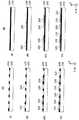
図1は上記カラーフィルタ基板の第1の実施形態を示す部分概略図である。図1(A)は、上面図であり、図1(B)は、図1(A)のa−a断面図であり、図1(C)は、図1(A)のb−b断面図である。図1(D)は、カラーフィルタ基板が重なった部分を部分的に拡大した図である。 FIG. 1 is a partial schematic view showing a first embodiment of the color filter substrate. 1A is a top view, FIG. 1B is an aa cross-sectional view of FIG. 1A, and FIG. 1C is a bb cross-section of FIG. 1A. FIG. FIG. 1D is a partially enlarged view of a portion where the color filter substrates overlap.
図1に示すように、本発明のカラーフィルタ基板(100)には、基板(102)上にブラックマトリックス(104)と、赤、緑および青の各色のカラーフィルタ層(106、108、110)が設けられている。ブラックマトリックスは、第1の方向および第2の方向に互いに直交して、格子状に設けられる。透明基板上のブラックマトリックスが設けられない開口部分(112)は、複数のサブピクセルに相当する部分である。本発明では、上記第1の方向に沿って、各色のカラーフィルタ層を形成することが好ましい。図1(A)では、紙面の上下方向(図1において座標で示されているX方向)を第1の方向としている。また、図1(A)の紙面の左右方向(図1において座標で示されているY方向)を第2の方向としている。 As shown in FIG. 1, the color filter substrate (100) of the present invention includes a black matrix (104) on a substrate (102) and color filter layers (106, 108, 110) of red, green and blue colors. Is provided. The black matrix is provided in a lattice shape orthogonal to each other in the first direction and the second direction. The opening portion (112) where the black matrix is not provided on the transparent substrate is a portion corresponding to a plurality of subpixels. In the present invention, it is preferable to form a color filter layer of each color along the first direction. In FIG. 1A, the vertical direction (the X direction indicated by coordinates in FIG. 1) is the first direction. Further, the left-right direction (the Y direction indicated by coordinates in FIG. 1) of the plane of FIG. 1A is the second direction.
第1の実施形態では、図1(A)および(B)に示したように、各カラーフィルタ層は、カラーフィルタ層の両端部に突出した部分、すなわち図1に示した座標のY方向に延在した部分(114、116、118)を有する。この突出した部分は、隣り合うカラーフィルタ層同士が、ブラックマトリックスの格子点の領域以外の部分で重なるように(すなわち柱状部を形成するように)、サブピクセルに相当する開口部(112)からブラックマトリックス上に延在している。 In the first embodiment, as shown in FIGS. 1A and 1B, each color filter layer has a protruding portion at both ends of the color filter layer, that is, in the Y direction of the coordinates shown in FIG. It has an extended part (114, 116, 118). The protruding portion is formed from the opening (112) corresponding to the sub-pixel so that the adjacent color filter layers overlap each other in a portion other than the black matrix lattice point region (that is, so as to form a columnar portion). Extends over the black matrix.
具体的には、図1(B)に示されるように、赤色カラーフィルタ層(106)の縁部(114)は、ブラックマトリックス(104)上で、一方の縁部が緑色カラーフィルタ層(108)の突出した縁部(116)で覆われ、他の一方の縁部が、青色カラーフィルタ層(110)の突出した縁部(118)で覆われており、これにより、色変換フィルタ基板には、それぞれ、ブラックマトリックス−赤色フィルタ層−青色フィルタ層の順で重なり合った部分(120)、並びに、ブラックマトリックス−赤色フィルタ層−緑色フィルタ層の順で重なり合った(120’)が存在する。 Specifically, as shown in FIG. 1B, the edge (114) of the red color filter layer (106) is on the black matrix (104), and one edge is the green color filter layer (108). ) Is covered with the protruding edge portion (116), and the other edge portion is covered with the protruding edge portion (118) of the blue color filter layer (110). , There are a portion (120) overlapping in the order of black matrix-red filter layer-blue filter layer (120) and a portion overlapping in the order of black matrix-red filter layer-green filter layer (120 ').
また、緑色カラーフィルタ層(108)は、その一方の縁部が赤色カラーフィルタ層(106)の突出した縁部(114)を覆い、他の一方の縁部が青色カラーフィルタ層(110)により覆われており、これにより、色変換フィルタ基板には、それぞれ、ブラックマトリックス−赤色フィルタ層−緑色フィルタ層の順で重なり合った部分(120’)、並びに、ブラックマトリックス−緑色フィルタ層−青色フィルタ層の順で重なり合った(120”)が存在する。 The green color filter layer (108) has one edge covering the protruding edge (114) of the red color filter layer (106), and the other edge is covered by the blue color filter layer (110). Accordingly, the color conversion filter substrate includes a portion (120 ′) overlapping in order of black matrix-red filter layer-green filter layer, and black matrix-green filter layer-blue filter layer, respectively. (120 ″) overlapped in this order.
さらに、青色カラーフィルタ層(110)は、その一方の縁部が緑色カラーフィルタ層(108)の突出した縁部(116)を覆い、他の一方の縁部が赤色カラーフィルタ層(106)を覆っており、これにより、色変換フィルタ基板には、それぞれ、ブラックマトリックス−赤色フィルタ層−青色フィルタ層の順で重なり合った部分(120)、並びに、ブラックマトリックス−緑色フィルタ層−青色フィルタ層の順で重なり合った(120”)が存在する。 Further, the blue color filter layer (110) has one edge covering the protruding edge (116) of the green color filter layer (108) and the other edge covering the red color filter layer (106). In this way, the color conversion filter substrate includes the overlapping portion (120) in the order of black matrix-red filter layer-blue filter layer, and the order of black matrix-green filter layer-blue filter layer, respectively. (120 ″) overlapped with each other.
なお、上述の重なり合いの順序は、各カラーフィルタ層を、赤色カラーフィルタ層、緑色カラーフィルタ層、青色カラーフィルタ層の順で形成した場合の例である。したがって、各色のカラーフィルタ層の形成順序を変えると、上記の重なり合いの順序は変化する。すなわち、三色のカラーフィルタ層のうち、最初に形成されるカラーフィルタ層の突出した縁部がブラックマトリックス上に形成され、次いで2番目に形成されるカラーフィルタ層の突出した縁部の一方が最初に形成されたカラーフィルタ層の縁部の上まで重なり、2番目に形成されるカラーフィルタ層の突出した縁部の他の一方は、ブラックマトリックス上に形成される。そして、3番目に形成されるカラーフィルタ層の突出した縁部は、最初および2番目に形成されたカラーフィルタ層の突出した縁部の上まで重なることになる。但し、最終的に形成される柱状部の構造は、各色のカラーフィルタ層をいずれの順序で形成した場合であっても同じである。 The order of overlap described above is an example in which the color filter layers are formed in the order of the red color filter layer, the green color filter layer, and the blue color filter layer. Therefore, when the formation order of the color filter layers of the respective colors is changed, the order of the above overlapping changes. That is, of the three color filter layers, the protruding edge of the first color filter layer is formed on the black matrix, and then one of the protruding edges of the second color filter layer is formed. The other one that overlaps over the edge of the first formed color filter layer and the protruding edge of the second formed color filter layer is formed on the black matrix. Then, the protruding edge of the third color filter layer overlaps with the protruding edge of the first and second formed color filter layers. However, the structure of the columnar portion finally formed is the same regardless of the order in which the color filter layers of the respective colors are formed.
また、第1の実施形態では、図1(A)および(C)に示したように、各カラーフィルタ層は、ブラックマトリックスの格子点の領域(図2(B)の「a」で示した領域)において、上述のような突出した縁部を有しておらず、上述のような重なり部分(柱状部)は存在しない。 In the first embodiment, as shown in FIGS. 1A and 1C, each color filter layer has a black matrix lattice point region (indicated by “a” in FIG. 2B). (Region) does not have a protruding edge as described above, and there is no overlapping portion (columnar portion) as described above.
具体的には、図1(C)に示したように、各カラーフィルタ層(106、108、110)は重なり合うことなくブラックマトリックス(104)上に形成されている。なお、図1(C)では、各カラーフィルタ層は、隣接するように図示してあるが、ブラックマトリックスの格子点領域においては、カラーフィルタ層は、必ずしも隣接している必要はない。 Specifically, as shown in FIG. 1C, the color filter layers (106, 108, 110) are formed on the black matrix (104) without overlapping. In FIG. 1C, the color filter layers are illustrated as being adjacent to each other; however, the color filter layers are not necessarily adjacent to each other in the lattice point region of the black matrix.
このように、本発明の第1の実施形態のカラーフィルタ基板では、隣り合ったカラーフィルタ層の縁部の一部が突出して、ブラックマトリックスの格子点の領域以外の部分でこの縁部が重なった構造を有している。このようにすることで、色変換フィルタ基板は、図2(A)に示したような、ブラックマトリックスの格子点以外の部分(図2(A)の「a」で示された領域)に、リブ(または支柱とも称する)に相当する柱状部が形成される。 As described above, in the color filter substrate of the first embodiment of the present invention, a part of the edge of the adjacent color filter layer protrudes, and this edge overlaps with a part other than the area of the lattice point of the black matrix. Have a structure. By doing in this way, the color conversion filter substrate has a portion other than the black matrix lattice points (region indicated by “a” in FIG. 2A) as shown in FIG. A columnar portion corresponding to a rib (or a column) is formed.
なお、カラーフィルタ層の突出した縁部の形状は、隣接したカラーフィルタ層が重なり合う限り、特に限定されない、例えば、三角形、矩形、台形状等、いずれの形状であってもよい。 Note that the shape of the protruding edge of the color filter layer is not particularly limited as long as adjacent color filter layers overlap each other, and may be any shape such as a triangle, a rectangle, a trapezoid, or the like.
この柱状部は、ブラックマトリックス(104)上において形成されるが、柱状部の最も厚い領域(最も高さのある領域)(図1(D)のM部分)の高さは、リブとして機能する高さであればよい。本発明では、例えば、カラーフィルタ層の2層分を併せた厚さでる。リブの好ましい高さは、2μm〜5μm、好ましくは3μm程度である。また、柱状部は、パターンニングのし易さから、図1(D)に示すように、ブラックマトリックスの幅の中央領域でブラックマトリックスおよび2種類のカラーフィルタ層が重なり合っていることが好ましい。本発明では、図1(D)に示すような、ブラックマトリックスと一色のカラーフィルタ層が重なっている部分(L部分およびN部分)と、ブラックマトリックス上に2種類のカラーフィルタ層が重なっている部分(M部分)の幅、r、r’およびr”とする。例えば、ブラックマトリックスが幅0.03mmで形成される場合、r’は0.01mm〜0.02mmである。しかし、カラーフィルタ基板を有機EL素子と貼り合わせる際に、柱状部の機械的強度が十分である限り、幅r’は、幅rまたは幅r”よりも狭くてもよく、逆に、幅rまたは幅r”よりも広くてもかまわない。 This columnar portion is formed on the black matrix (104). The height of the thickest region (the region with the highest height) (M portion in FIG. 1D) of the columnar portion functions as a rib. Any height is sufficient. In the present invention, for example, the thickness is the combined thickness of two color filter layers. The preferred height of the rib is 2 μm to 5 μm, preferably about 3 μm. In addition, the columnar portion preferably has a black matrix and two types of color filter layers overlapping in the central region of the width of the black matrix, as shown in FIG. 1D, for ease of patterning. In the present invention, as shown in FIG. 1D, a portion where the black matrix and the color filter layer of one color overlap (L portion and N portion) and two kinds of color filter layers overlap on the black matrix. The width of the portion (M portion), r, r ′, and r ″. For example, when the black matrix is formed with a width of 0.03 mm, r ′ is 0.01 mm to 0.02 mm. When the substrate is bonded to the organic EL element, the width r ′ may be narrower than the width r or the width r ″ as long as the mechanical strength of the columnar portion is sufficient, and conversely, the width r or the width r ″. It doesn't matter if it's wider.
本発明では、上述のような柱状部の構造とすることで、後述するような有機EL素子と貼り合わせて充填剤を充填する際に、柱状部の形成されていない部分から充填剤が広がり、充填剤の充填が容易となる。 In the present invention, the structure of the columnar portion as described above allows the filler to spread from the portion where the columnar portion is not formed when the filler is filled with the organic EL element as will be described later. Filling with a filler becomes easy.
また、本発明では、柱状部はカラーフィルタ層の端部の一部を突出させているので、十分な機械的強度が保持できる。 In the present invention, since the columnar portion projects a part of the end portion of the color filter layer, sufficient mechanical strength can be maintained.
次に、本発明のカラーフィルタ基板の第2の実施形態について、図3を参照して説明する。図3(A)は、上面図であり、図3(B)は、図3(A)のa−a断面図であり、図3(C)は、図3(A)のb−b断面図である。 Next, a second embodiment of the color filter substrate of the present invention will be described with reference to FIG. 3A is a top view, FIG. 3B is an aa cross-sectional view of FIG. 3A, and FIG. 3C is a bb cross-section of FIG. 3A. FIG.
図3(A)から(C)に示したように、第2の実施形態では、各カラーフィルタ層(106、108、110)は、図3(A)に示したように、ブラックマトリックス(104)の第1の方向に沿って形成される。また、各カラーフィルタ層(106、108、110)は、図3(B)に示したように、ブラックマトリックスの第2の方向(図3に示した座標のY軸方向(図1のY軸方向と同じ))であって、ブラックマトリックスの格子点の領域に、突出した縁部(114、116、118)を有する。したがって、カラーフィルタ層により形成される柱状部(120、120’、120”)は、ブラックマトリックス(104)の格子点の領域(図2(B)の「a」で示された領域)に存在する。なお、図3(B)における各カラーフィルタ層の突出した縁部による重なりの様式、および柱状部の厚み、突出した縁部の形状などは、第1の実施形態で説明した通りである。なお、第2の実施形態においては、柱状部の重なり部分の幅は、例えば、第1の実施形態で説明したとおり、例えば、ブラックマトリックスが幅0.03mmで形成される場合、0.01mmとした。しかし、カラーフィルタ基板を有機EL素子と貼り合わせる際に、柱状部の機械的強度が十分である限り、重なりの幅は、これよりも狭くてもよく、逆に、これよりも広くてもかまわない。 As shown in FIGS. 3A to 3C, in the second embodiment, each color filter layer (106, 108, 110) has a black matrix (104) as shown in FIG. ) Along the first direction. Further, as shown in FIG. 3B, each color filter layer (106, 108, 110) is arranged in the second direction of the black matrix (the Y-axis direction of the coordinates shown in FIG. 3 (the Y-axis in FIG. 1)). The same as the direction)) and has protruding edges (114, 116, 118) in the region of the black matrix grid points. Therefore, the columnar portions (120, 120 ′, 120 ″) formed by the color filter layer are present in the lattice point region of the black matrix (104) (the region indicated by “a” in FIG. 2B). To do. It should be noted that the manner of overlapping the protruding edge portions of each color filter layer in FIG. 3B, the thickness of the columnar portion, the shape of the protruding edge portion, and the like are as described in the first embodiment. In the second embodiment, the width of the overlapping portion of the columnar portions is, for example, 0.01 mm when the black matrix is formed with a width of 0.03 mm as described in the first embodiment. did. However, when the color filter substrate is bonded to the organic EL element, as long as the mechanical strength of the columnar part is sufficient, the overlap width may be narrower than this, and conversely, it may be wider. Absent.
また、第2の実施形態では、図3(A)および(C)に示したように、各カラーフィルタ層は、ブラックマトリックスの格子点以外の領域(図2(A)の「a」で示した領域)において、上述のような突出した縁部を有しておらず、上述のような重なり部分(柱状部)は存在しない。 In the second embodiment, as shown in FIGS. 3A and 3C, each color filter layer has a region other than the lattice point of the black matrix (indicated by “a” in FIG. 2A). In this case, there is no protruding edge as described above, and there is no overlapping portion (columnar portion) as described above.
具体的には、図3(C)に示したように、各カラーフィルタ層(106、108、110)は、サブピクセル間のブラックマトリックス(104)の形成されている領域上で重なり合うことなく形成されている。なお、図3(C)では、各カラーフィルタ層は、隣接するように図示してあるが、ブラックマトリックスの形成されている領域に一部重なるようにして、形成されていればよく、ブラックマトリックス上で接触している必要はない。例えば、ブラックマトリックスが幅0.03mmで形成される場合、各色のカラーフィルタ層は、0.01mm〜0.02mm程度ブラックマトリックス上に一部重なって形成されていることが好ましい。しかし、重なりの幅は、ブラックマトリックスと一部重なっている限り、これよりも狭くてもよく、逆に、これよりも広くてもかまわない。 Specifically, as shown in FIG. 3C, each color filter layer (106, 108, 110) is formed without overlapping on a region where a black matrix (104) between sub-pixels is formed. Has been. In FIG. 3C, the color filter layers are illustrated so as to be adjacent to each other, but may be formed so as to partially overlap a region where the black matrix is formed. There is no need to touch on. For example, when the black matrix is formed with a width of 0.03 mm, the color filter layers of the respective colors are preferably formed so as to partially overlap the black matrix by about 0.01 mm to 0.02 mm. However, the overlap width may be narrower than this as long as it partially overlaps with the black matrix, and conversely, it may be wider than this.
なお、本発明のカラーフィルタ基板は、上記構成に加え、カラーフィルタ層上にガスバリア層を設けてもよい。ガスバリア層は、外部環境からの酸素、低分子成分および水分の透過を防止することができるものである。ガスバリア層は、任意選択の層であるが、後述するように、本発明のカラーフィルタ基板を有機EL素子と組み合わせて、カラー有機EL素子を形成する場合、有機EL層の機能低下を防止することに有効である。したがって、この目的のために、ガスバリア層を設けることが好ましい。 In addition to the above configuration, the color filter substrate of the present invention may be provided with a gas barrier layer on the color filter layer. The gas barrier layer can prevent permeation of oxygen, low molecular components and moisture from the external environment. Although the gas barrier layer is an optional layer, as described later, when the color organic EL element is formed by combining the color filter substrate of the present invention with the organic EL element, the deterioration of the function of the organic EL layer is prevented. It is effective for. Therefore, it is preferable to provide a gas barrier layer for this purpose.
本発明のカラーフィルタ基板は、カラー表示素子の構成要素として用いることができるが、この場合、表示素子の発光部には白色光を発するものを選択すればよい。 The color filter substrate of the present invention can be used as a component of a color display element. In this case, a light emitting part of the display element may be selected that emits white light.
以下に、カラーフィルタ基板の各構成要素について説明する。
I)透明基板(102)
透明基板(102)の材料として好ましいものは、ガラス、ポリエチレンテレフタレート、ポリメチルメタクリレート等の樹脂を含む。ホウケイ酸ガラスまたは青板ガラス等が特に好ましいものである。Hereinafter, each component of the color filter substrate will be described.
I) Transparent substrate (102)
Preferred materials for the transparent substrate (102) include resins such as glass, polyethylene terephthalate and polymethyl methacrylate. Borosilicate glass or blue plate glass is particularly preferable.
II)ブラックマトリックス(104)
各色に対応するカラーフィルタ層の間の領域には、ブラックマトリックス(104)を形成する。ブラックマトリックスを設けることによって、隣接するサブピクセルの色変換フィルタ層への光の漏れを防止して、にじみのない所望される蛍光変換色のみを得ることが可能となる。後述する有機ELディスプレイの封止を妨げないことが好ましい。ブラックマトリックスの材料は、従来から用いられているものをそのまま使用することができる。例えば、カラーモザイクCK7800(富士フイルムエレクトロニクスマテリアルズ(株)製)などを用いることができる。ブラックマトリックス(104)は、好ましくは0.5〜2.0μmの厚さを有する。II) Black matrix (104)
A black matrix (104) is formed in a region between the color filter layers corresponding to each color. By providing the black matrix, it is possible to prevent leakage of light to the color conversion filter layer of the adjacent subpixel and obtain only a desired fluorescence conversion color without blur. It is preferable not to prevent sealing of the organic EL display described later. As the material of the black matrix, a conventionally used material can be used as it is. For example, color mosaic CK7800 (manufactured by Fuji Film Electronics Materials Co., Ltd.) can be used. The black matrix (104) preferably has a thickness of 0.5 to 2.0 μm.
III)カラーフィルタ層
本発明におけるカラーフィルタ層は、従来から用いられている材料から形成することができる。例えば、赤色カラーフィルタ層としてカラーモザイクCR−7001、緑色カラーフィルタ層としてカラーモザイクCG−7001、青色カラーフィルタ層としてカラーモザイクCB−7001(各々、富士フィルムエレクトロニクスマテリアルズ社製)等を用いることができる。III) Color filter layer The color filter layer in this invention can be formed from the material used conventionally. For example, a color mosaic CR-7001 as a red color filter layer, a color mosaic CG-7001 as a green color filter layer, a color mosaic CB-7001 (each manufactured by Fuji Film Electronics Materials) as a blue color filter layer, or the like may be used. it can.
IV)ガスバリア層
本発明では、カラーフィルタ層を覆うガスバリア層(図示せず)を設けることが好ましい。ガスバリア層は、可視域における透明性が高く(400〜800nmの範囲で透過率50%以上)、電気絶縁性を有し、水分、酸素および低分子成分に対するバリア性を有し、好ましくは鉛筆硬度2H以上の膜硬度を有する材料で形成される。例えば、SiOx、SiNx、SiNxOy、AlOx、TiOx、TaOx、ZnOx等の無機酸化物、無機窒化物等の材料を使用できる。IV) Gas Barrier Layer In the present invention, it is preferable to provide a gas barrier layer (not shown) that covers the color filter layer. The gas barrier layer has high transparency in the visible region (transmittance of 50% or more in the range of 400 to 800 nm), electrical insulation, barrier properties against moisture, oxygen and low molecular components, preferably pencil hardness. It is formed of a material having a film hardness of 2H or more. For example, materials such as inorganic oxides and inorganic nitrides such as SiOx , SiNx , SiNx Oy , AlOx , TiOx , TaOx , and ZnOx can be used.
ガスバリア層は、0.1〜1μm程度の厚さを有することができる。本発明では、ガスバリア層は、柱状部をトレースできる膜厚でなければならない。 The gas barrier layer may have a thickness of about 0.1 to 1 μm. In the present invention, the gas barrier layer must have a thickness that can trace the columnar portion.
次に、本発明のカラーフィルタ基板の製造方法を説明する。本発明の製造方法は、(i)透明基板上において格子状にブラックマトリックスを形成する工程と、(ii)該透明基板上において、ブラックマトリックスの第1の方向に沿って複数のカラーフィルタ層を形成する工程を少なくとも含み、該カラーフィルタ層の端部の一部がブラックマトリックスの格子点領域または該格子点領域以外の第1の方向のブラックマトリックスの領域で重なるように延在して形成されることを特徴とする。 Next, a method for manufacturing the color filter substrate of the present invention will be described. The manufacturing method of the present invention includes (i) a step of forming a black matrix in a lattice shape on a transparent substrate, and (ii) a plurality of color filter layers along the first direction of the black matrix on the transparent substrate. Forming at least a step of forming the color filter layer so that a part of the end portion of the color filter layer overlaps with a lattice point region of the black matrix or a region of the black matrix in the first direction other than the lattice point region. It is characterized by that.
以下に、図4を参照して製造方法を説明する。以下の説明では、図1に示した第1の実施形態のカラーフィルタ基板を例に取る。図4(A)および(B)は本発明の製造工程を説明するための図であるが、それぞれ図1のa−a断面に相当する部分およびb−b断面に相当する部分の工程図である。 Below, a manufacturing method is demonstrated with reference to FIG. In the following description, the color filter substrate of the first embodiment shown in FIG. 1 is taken as an example. FIGS. 4A and 4B are views for explaining the manufacturing process of the present invention. FIG. 4A is a process diagram of a portion corresponding to the aa cross section and a portion corresponding to the bb cross section in FIG. is there.
(i)第1の工程(図4(A)(i)、(B)(i))
第1の工程は、透明基板(102)上において格子状にブラックマトリックス(104)を形成する工程である。ブラックマトリックスは、スピンコート法とフォトレジスト法を組み合わせた湿式法などにより形成することができる。例えば、ブラックマトリックスの材料をスピンコート法により透明基板の全面に塗布し、次いでフォトリソグラフィー法により、第1の方向および第2の方向(例えば、図1のXおよびY方向)が互いに直交する格子状のパターンに、パターンニングすればよい。(I) 1st process (FIG. 4 (A) (i), (B) (i))
The first step is a step of forming a black matrix (104) in a lattice pattern on the transparent substrate (102). The black matrix can be formed by a wet method combining a spin coating method and a photoresist method. For example, a black matrix material is applied to the entire surface of a transparent substrate by a spin coating method, and then a lattice in which a first direction and a second direction (for example, the X and Y directions in FIG. 1) are orthogonal to each other by a photolithography method. What is necessary is just to pattern into a pattern.
(ii)第2の工程(図4(A)(ii)〜(iv)、(B)(ii)〜(iv))
第2の工程は、透明基板(102)上において、ブラックマトリックス(104)の第1の方向に沿って複数のカラーフィルタ層(106、108、110)を形成する工程である。(Ii) 2nd process (FIG. 4 (A) (ii)-(iv), (B) (ii)-(iv))
The second step is a step of forming a plurality of color filter layers (106, 108, 110) along the first direction of the black matrix (104) on the transparent substrate (102).
本工程では、上述の第1の実施形態および第2の実施形態のそれぞれのカラーフィルタ基板に応じて、各色カラーフィルタ層の重なり部分(柱状部が形成される部分)の位置が異なるので、それぞれの実施形態に沿った位置に各色カラーフィルタ層の重なり部分ができるようにパターンニングを行う。 In this step, the position of the overlapping portion (the portion where the columnar portion is formed) of each color filter layer differs depending on the color filter substrate of the first embodiment and the second embodiment described above. Patterning is performed so that an overlapping portion of each color filter layer is formed at a position along the embodiment.
第1の実施形態のカラーフィルタ基板の製造方法については、第2工程は、図4(A)(ii)〜(iv)、(B)(ii)〜(iv)に示したように、各色のカラーフィルタ層を順次ブラックマトリックスの第1の方向(図4においては、座標のX方向)に沿って形成することを含む。この際、図4(A)(ii)〜(iv)に示したように、ブラックマトリックスの格子点の領域以外の部分(すなわち、サブピクセル間)で、隣り合ったカラーフィルタ層の縁部の一部が突出して、この縁部が重なるようにパターンニングを行う。このようにすることで、色変換フィルタ基板は、図2(A)に示したような、ブラックマトリックスの格子点以外の部分(図2(A)の「a」で示された領域)に、リブに相当する柱状部が形成される。 As for the manufacturing method of the color filter substrate of the first embodiment, each of the second steps is performed as shown in FIGS. 4 (A) (ii) to (iv) and (B) (ii) to (iv). The color filter layers are sequentially formed along the first direction of the black matrix (the X direction of the coordinates in FIG. 4). At this time, as shown in FIGS. 4 (A) (ii) to (iv), the edge of the color filter layer adjacent to each other in the portion other than the region of the lattice point of the black matrix (that is, between subpixels). Patterning is performed so that a part protrudes and this edge part overlaps. By doing in this way, the color conversion filter substrate has a portion other than the black matrix lattice points (region indicated by “a” in FIG. 2A) as shown in FIG. Columnar portions corresponding to the ribs are formed.
各色カラーフィルタ層の成膜は、例えば、以下のように行うことができる。まず、スピンコート法によりブラックマトリックス(104)を形成した透明基板(102)上に、第1のカラーフィルタ層(例えば赤色カラーフィルタ層)の材料を塗布し、フォトリソグラフィー法によりパターンニングして、ブラックマトリックスの格子点の領域以外の部分(すなわち、サブピクセル間)にカラーフィルタ層の縁部の一部が突出するように、第1のカラーフィルタ層を形成する。次いで、第1のカラーフィルタ層の成膜と同様の手順で、第2および第3のカラーフィルタ層を形成すればよい。このようにすることで、ブラックマトリックスの格子点の領域以外の部分(すなわち、サブピクセル間)で、隣り合ったカラーフィルタ層の縁部の一部が重なって、柱状部を形成できる。 Each color filter layer can be formed as follows, for example. First, a material for a first color filter layer (for example, a red color filter layer) is applied on a transparent substrate (102) on which a black matrix (104) is formed by spin coating, and is patterned by photolithography. The first color filter layer is formed so that a part of the edge of the color filter layer protrudes in a portion other than the black matrix lattice point region (that is, between subpixels). Next, the second and third color filter layers may be formed in the same procedure as the formation of the first color filter layer. By doing so, a part of the edge of the adjacent color filter layer overlaps in a portion (that is, between subpixels) other than the region of the grid point of the black matrix, thereby forming a columnar portion.
第2の実施形態のカラーフィルタ基板の製造方法は、上述の第1の実施形態の場合とほぼ同じである。但し、第2工程において、ブラックマトリックスの格子点領域の部分で、隣り合ったカラーフィルタ層の縁部の一部が突出して、この縁部が重なるようにパターンニングを行う。このようにすることで、色変換フィルタ基板は、図2(B)に示したような、ブラックマトリックスの格子点領域の部分(図2(B)の「a」で示された領域)に、リブに相当する柱状部が形成される。 The manufacturing method of the color filter substrate of the second embodiment is almost the same as that of the above-described first embodiment. However, in the second step, patterning is performed so that a part of the edge of the adjacent color filter layer protrudes at the lattice point area of the black matrix and the edge overlaps. By doing in this way, the color conversion filter substrate can be applied to the portion of the black matrix lattice point region (the region indicated by “a” in FIG. 2B) as shown in FIG. Columnar portions corresponding to the ribs are formed.
上記製造方法で形成される柱状部の形状、寸法等の諸条件は先に説明した通りである。 Various conditions such as the shape and dimensions of the columnar portion formed by the above manufacturing method are as described above.
本発明のカラーフィルタ基板には、カラーフィルタ層上に任意選択的な層としてガスバリア層を形成することができる。ガスバリア層は、透明基板上のブラックマトリックスおよび各色カラーフィルタ層を覆うように形成することが好ましいが、柱状部の形状をトレースしていなければならない。ガスバリア層の形成方法としては特に制約はなく、スパッタ法、CVD法、真空蒸着法、ディップ法、ゾル−ゲル法等の慣用の手法により形成できる。 In the color filter substrate of the present invention, a gas barrier layer can be formed as an optional layer on the color filter layer. The gas barrier layer is preferably formed so as to cover the black matrix and each color filter layer on the transparent substrate, but the shape of the columnar portion must be traced. There is no restriction | limiting in particular as a formation method of a gas barrier layer, It can form by common methods, such as a sputtering method, CVD method, a vacuum evaporation method, a dip method, a sol-gel method.
次に、本発明の色変換フィルタ基板について説明する。本発明の色変換フィルタ基板は、透明基板と、該透明基板上において格子状に設けられたブラックマトリックスと、該透明基板上において、該ブラックマトリックスの第1の方向に沿って設けられた複数のカラーフィルタ層と、該カラーフィルタ層上において、該ブラックマトリックスの第1の方向に沿って設けられた複数の色変換層を少なくとも含み、該色変換層の端部の一部がブラックマトリックスの格子点領域または該格子点領域以外の第1の方向のブラックマトリックスの領域で重なるように延在していることを特徴とする。 Next, the color conversion filter substrate of the present invention will be described. The color conversion filter substrate of the present invention includes a transparent substrate, a black matrix provided in a lattice pattern on the transparent substrate, and a plurality of black matrixes provided along the first direction of the black matrix on the transparent substrate. A color filter layer and at least a plurality of color conversion layers provided along the first direction of the black matrix on the color filter layer, wherein a part of the end of the color conversion layer is a lattice of a black matrix It extends so that it may overlap in the area | region of the black matrix of a 1st direction other than a point area | region or this lattice point area | region.
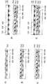
図5は上記色変換フィルタ基板の第1の実施形態を示す部分概略図である。図5(A)は、上面図であり、図5(B)は、図5(A)のa−a断面図であり、図5(C)は、図5(A)のb−b断面図である。図5(D)は、色変換フィルタ基板の、色変換層が重なった部分を部分的に拡大した図であり、透明基板とブラックマトリックス部分と、色変換層の重なり合っている上部を表す。なお、図5においては、図1を用いて先に説明したのと同様の方向付けで以下の説明を行う。すなわち、図5では、紙面の上下方向(図5において座標で示されているX方向)を第1の方向とし、図5の紙面の左右方向(図5において座標で示されているY方向)を第2の方向としている。 FIG. 5 is a partial schematic view showing a first embodiment of the color conversion filter substrate. 5A is a top view, FIG. 5B is an aa cross-sectional view of FIG. 5A, and FIG. 5C is a bb cross-section of FIG. 5A. FIG. FIG. 5D is a partially enlarged view of the color conversion filter substrate where the color conversion layers overlap, and represents the upper portion where the transparent substrate, the black matrix portion, and the color conversion layer overlap. In FIG. 5, the following description will be given with the same orientation as described above with reference to FIG. That is, in FIG. 5, the vertical direction (X direction indicated by coordinates in FIG. 5) is the first direction, and the left and right direction (Y direction indicated by coordinates in FIG. 5) of FIG. 5 is the first direction. Is the second direction.
図5に示すように、本発明の色変換フィルタ基板(200)には、基板(102)上にブラックマトリックス(104)と、色変換フィルタ層が設けられる。色変換フィルタ層には、赤、緑および青の各色のカラーフィルタ層(106、108、110)と、赤、緑および青の各色色変換層(506、508、510)が含まれる。なお、カラーフィルタ層は、上述のカラーフィルタ基板で説明した通りのものである。 As shown in FIG. 5, the color conversion filter substrate (200) of the present invention is provided with a black matrix (104) and a color conversion filter layer on the substrate (102). The color conversion filter layer includes a color filter layer (106, 108, 110) for each color of red, green, and blue, and a color conversion layer (506, 508, 510) for each color of red, green, and blue. The color filter layer is as described in the above color filter substrate.
本明細書においては、色変換フィルタ層の用語を用いるが、この用語は、カラーフィルタ層(106、108、110)、色変換層(506、508、510)、およびカラーフィルタ層と色変換層との積層体の総称として用いる。 In this specification, the term of the color conversion filter layer is used, and this term includes the color filter layer (106, 108, 110), the color conversion layer (506, 508, 510), and the color filter layer and the color conversion layer. It is used as a general term for the laminate.
色変換層は、後述するカラー有機EL素子の一部として用いられる場合、有機EL層で発光される近紫外領域ないし可視領域の光、特に青色ないし青緑色領域の光を吸収して異なる波長の可視光を蛍光として発光するものである。フルカラー表示を可能にするためには、少なくとも青色(B)領域、緑色(G)領域および赤色(R)領域の光を放出する独立した色変換層が設けられる。有機EL層が青色から青緑色の光を発する場合、青色領域には、青色カラーフィルタ層のみを用いることができ、このようにすることが好ましい。この場合、青色変換層(510)が形成される部分には、透明層を、赤色および緑色の色変換層の膜厚と同等の膜厚で形成する必要がある。RGBそれぞれの色変換層は、少なくとも有機蛍光色素とマトリクス樹脂とを含む。 When the color conversion layer is used as a part of a color organic EL element described later, it absorbs light in the near ultraviolet region or visible region emitted from the organic EL layer, in particular, light in a blue or blue-green region, and has a different wavelength. Visible light is emitted as fluorescence. In order to enable full color display, an independent color conversion layer that emits light in at least the blue (B) region, the green (G) region, and the red (R) region is provided. When the organic EL layer emits blue to blue-green light, only the blue color filter layer can be used in the blue region, and this is preferable. In this case, it is necessary to form a transparent layer with a film thickness equivalent to the film thickness of the red and green color conversion layers in a portion where the blue conversion layer (510) is formed. Each of the RGB color conversion layers includes at least an organic fluorescent dye and a matrix resin.
ブラックマトリックスは、上述したカラーフィルタ基板で説明した通りの構成とすることができる。また、各カラーフィルタ層(106、108、110)は、図5(B)および(C)に示したように、ブラックマトリックスの第1の方向(図5(B)の座標でX方向)に沿って形成されるが、ブラックマトリックスの格子点以外の領域(サブピクセル間)および格子点領域で互いに重なり合うことなく設けられる。なお、図5(B)および(C)では、各カラーフィルタ層は、互いに隣り合うカラーフィルタ層同士で隣接するように図示されているが、これらは必ずしも隣接している必要はない。 The black matrix can be configured as described for the color filter substrate described above. Further, as shown in FIGS. 5B and 5C, the color filter layers (106, 108, 110) are arranged in the first direction of the black matrix (X direction in the coordinates of FIG. 5B). However, they are provided so as not to overlap each other in a region other than the lattice points of the black matrix (between subpixels) and the lattice point region. 5B and 5C, the color filter layers are illustrated so as to be adjacent to each other adjacent to each other, but they are not necessarily adjacent to each other.
第1の実施形態では、図5(A)および(B)に示したように、各色変換層は、色変換層の両端部に突出した部分、すなわち図5に示した座標のY方向に延在した部分(514、516、518)を有する。この突出した部分は、隣り合うカラーフィルタ層同士が、ブラックマトリックスの格子点の領域以外の部分で重なるように(すなわち柱状部を形成するように)、サブピクセルに相当する開口部(112)からブラックマトリックスとカラーフィルタ層の縁部上に延在している。 In the first embodiment, as shown in FIGS. 5A and 5B, each color conversion layer extends in a portion protruding from both ends of the color conversion layer, that is, in the Y direction of the coordinates shown in FIG. Existing part (514, 516, 518). The protruding portion is formed from the opening (112) corresponding to the sub-pixel so that the adjacent color filter layers overlap each other in a portion other than the black matrix lattice point region (that is, so as to form a columnar portion). Extending over the edges of the black matrix and the color filter layer.
具体的には、図5(B)に示されるように、赤色変換層(506)の縁部(514)は、ブラックマトリックス(104)の存在する領域上で、一方の縁部が緑色変換層(508)の突出した縁部(516)で覆われ、他の一方の縁部が、青色変換層(または、透明層)(510)の突出した縁部(518)で覆われており、これにより、色変換フィルタ基板には、それぞれ、ブラックマトリックス−カラーフィルタ層−赤色変換層−青色変換層(または透明層)の順で重なり合った部分(520)、並びに、ブラックマトリックス−カラーフィルタ層−赤色変換層−緑色変換層の順で重なり合った(120’)が存在する。 Specifically, as shown in FIG. 5B, the edge (514) of the red conversion layer (506) is on the region where the black matrix (104) is present, and one edge is the green conversion layer. (508) is covered with the protruding edge (516), and the other edge is covered with the protruding edge (518) of the blue conversion layer (or transparent layer) (510). Thus, the color conversion filter substrate includes a portion (520) in which the black matrix, the color filter layer, the red conversion layer, the blue conversion layer (or the transparent layer) overlap in this order, and the black matrix, the color filter layer, and the red color. There are (120 ′) overlapping in the order of conversion layer-green conversion layer.
また、緑色変換層(508)は、その一方の縁部が赤色変換層(506)の突出した縁部(514)を覆い、他の一方の縁部が青色変換層(または透明層)(510)により覆われており、これにより、色変換フィルタ基板には、それぞれ、ブラックマトリックス−カラーフィルタ層−赤色変換層−緑色変換層の順で重なり合った部分(520’)、並びに、ブラックマトリックス−カラーフィルタ層−緑色変換層−青色変換層(または透明層)の順で重なり合った(520”)が存在する。 The green conversion layer (508) has one edge covering the protruding edge (514) of the red conversion layer (506), and the other edge being the blue conversion layer (or transparent layer) (510). As a result, the color conversion filter substrate has a black matrix-color filter layer-red conversion layer-green conversion layer overlapping portion (520 ') and black matrix-color, respectively. There is an overlap (520 ") in the order of filter layer-green conversion layer-blue conversion layer (or transparent layer).
さらに、青色変換層(または透明層)(510)は、その一方の縁部が緑色変換層(508)の突出した縁部(516)を覆い、他の一方の縁部が赤色変換層(506)を覆っており、これにより、色変換フィルタ基板には、それぞれ、ブラックマトリックス−カラーフィルタ層−緑色変換層−青色変換層(または透明層)の順で重なり合った部分(520”)、並びに、ブラックマトリックス−カラーフィルタ層−赤色変換層−青色変換層(透明層)の順で重なり合った(520)が存在する。 Further, the blue conversion layer (or transparent layer) (510) has one edge covering the protruding edge (516) of the green conversion layer (508) and the other edge is the red conversion layer (506). In this way, the color conversion filter substrate includes a portion (520 ″) overlapping in the order of black matrix-color filter layer-green conversion layer-blue conversion layer (or transparent layer), and There is an overlap (520) in the order of black matrix-color filter layer-red conversion layer-blue conversion layer (transparent layer).
なお、上述の重なり合いの順序は、各色変換層を、赤色変換層、緑色変換層、青色変換層の順で形成した場合の例である。したがって、各色の色変換層の形成順序を変えると、上記の重なり合いの順序は変化する。すなわち、三色の色変換層のうち、最初に形成される色変換層の突出した縁部が、カラーフィルタ層上で、且つブラックマトリックスが形成されている領域上に形成され、次いで2番目の色変換層の突出した縁部の一方が最初に形成された色変換層の縁部の上まで重なり、2番目に形成される色変換層の突出した縁部の他の一方は、カラーフィルタ層上に形成される。そして、3番目に形成される色変換層の突出した縁部は、最初および2番目に形成された色変換層の突出した縁部の上まで重なることになる。但し、最終的に形成される柱状部の構造は、各色の色変換層をいずれの順序で形成した場合であっても同じである。 Note that the above-described overlapping order is an example in which each color conversion layer is formed in the order of a red conversion layer, a green conversion layer, and a blue conversion layer. Therefore, if the order of forming the color conversion layers for each color is changed, the order of the above-described overlapping changes. That is, of the three color conversion layers, the protruding edge of the first color conversion layer is formed on the color filter layer and the region where the black matrix is formed, and then the second color conversion layer is formed. One of the protruding edges of the color conversion layer overlaps the edge of the color conversion layer formed first, and the other of the protruding edges of the color conversion layer formed second is the color filter layer. Formed on top. Then, the protruding edge portion of the third color conversion layer is overlapped with the protruding edge portion of the first and second color conversion layers. However, the structure of the columnar portion finally formed is the same regardless of the order in which the color conversion layers of the respective colors are formed.
また、第1の実施形態では、図5(A)および(C)に示したように、各カラーフィルタ層は、ブラックマトリックスの格子点の領域(図2(B)の「a」で示した領域)において、上述のような突出した縁部を有しておらず、上述のような重なり部分(柱状部)は存在しない。 In the first embodiment, as shown in FIGS. 5A and 5C, each color filter layer is indicated by a lattice point region of the black matrix (indicated by “a” in FIG. 2B). (Region) does not have a protruding edge as described above, and there is no overlapping portion (columnar portion) as described above.
具体的には、図5(C)に示したように、各カラーフィルタ層(506、508、510)は重なり合うことなくブラックマトリックス(104)の形成されている領域の上に形成されている。なお、図5(C)では、各色変換層は、隣接するように図示してあるが、ブラックマトリックスの格子点領域においては、必ずしも隣接している必要はない。 Specifically, as shown in FIG. 5C, each color filter layer (506, 508, 510) is formed on a region where the black matrix (104) is formed without overlapping. In FIG. 5C, the color conversion layers are illustrated so as to be adjacent to each other. However, in the lattice point region of the black matrix, it is not always necessary to be adjacent.
このように、本発明の第1の実施形態の色変換フィルタ基板では、隣り合った色変換層の縁部の一部が突出して、ブラックマトリックスの格子点の領域以外の部分でこの縁部が重なった構造を有している。このようにすることで、色変換フィルタ基板は、図2(A)に示したような、ブラックマトリックスの格子点以外の領域(図2(A)の「a」で示された領域)に、リブに相当する柱状部が形成される。 As described above, in the color conversion filter substrate of the first embodiment of the present invention, a part of the edge of the adjacent color conversion layer protrudes, and this edge is in a part other than the area of the lattice point of the black matrix. It has an overlapping structure. By doing in this way, the color conversion filter substrate is in a region other than the black matrix lattice points (region indicated by “a” in FIG. 2A) as shown in FIG. Columnar portions corresponding to the ribs are formed.
なお、色変換層の突出した縁部の形状は、隣接した色変換層が重なり合う限り、特に限定されない、例えば、三角形、矩形、台形状等、いずれの形状であってもよい。 Note that the shape of the protruding edge of the color conversion layer is not particularly limited as long as adjacent color conversion layers overlap, and may be any shape such as a triangle, a rectangle, a trapezoid, or the like.
この柱状部は、ブラックマトリックス(504)が形成されている領域において形成されるが、柱状部の最も厚い領域(最も高さのある領域)(図5(D)のM部分)の高さは、リブとして機能する高さであればよい。本発明では、色変換層2層分を併せた厚さとすることができる。好ましい厚さは、3μm〜15μm、好ましくは5μm〜10μmである。また、柱状部は、パターンニングのし易さから、図5(D)に示すように、ブラックマトリックスの幅の中央部に相当する領域で2種類の色変換層が重なり合っていることが好ましい。本発明では、図5(D)に示すような、ブラックマトリックスと一色の色変換層が重り合った領域(L部分およびN部分)と、ブラックマトリックス上に2種類の色変換層が重なり合った領域(M部分)の幅、r、r’およびr”とする。例えば、ブラックマトリックスが幅0.03mmで形成される場合、r’は0.01mm〜0.02mmであることが好ましい。しかし、色変換フィルタ基板を有機EL素子と貼り合わせる際に、柱状部の機械的強度が十分である限り、幅r’は、幅rまたは幅r”よりも狭くてもよく、逆に、幅rまたは幅r”よりも広くてもかまわない。また、各色変換層の突出した縁部が重なり合った部分の各色変換層の厚さはパターニングの際の条件により種々異なる。好ましくは、この部分の厚さは同じである。 This columnar portion is formed in a region where the black matrix (504) is formed, and the height of the thickest region (the region with the highest height) of the columnar portion (M portion in FIG. 5D) is Any height that functions as a rib may be used. In the present invention, the thickness of the two color conversion layers can be combined. The preferred thickness is 3 μm to 15 μm, preferably 5 μm to 10 μm. Further, the columnar portion preferably has two types of color conversion layers overlapping in a region corresponding to the central portion of the width of the black matrix as shown in FIG. In the present invention, as shown in FIG. 5D, a region where the black matrix and one color conversion layer overlap (L portion and N portion) and a region where two types of color conversion layers overlap on the black matrix. For example, when the black matrix is formed with a width of 0.03 mm, r ′ is preferably 0.01 mm to 0.02 mm. When the color conversion filter substrate is bonded to the organic EL element, the width r ′ may be narrower than the width r or the width r ″ as long as the mechanical strength of the columnar portion is sufficient. It may be wider than the width r ″. Further, the thickness of each color conversion layer in the portion where the protruding edge of each color conversion layer overlaps varies depending on the patterning conditions. Preferably, the thickness of this portion Are the same
本発明では、上述のような柱状部の構造とすることで、後述するような有機EL素子と貼り合わせて充填剤を充填する際に、柱状部の形成されていない部分から充填剤が広がり、充填剤の充填が容易となる。 In the present invention, the structure of the columnar portion as described above allows the filler to spread from the portion where the columnar portion is not formed when the filler is filled with the organic EL element as will be described later. Filling with a filler becomes easy.
また、本発明では、柱状部は色変換層の端部の一部を突出させているので、十分な機械的強度が保持できる。 In the present invention, since the columnar portion projects part of the end of the color conversion layer, sufficient mechanical strength can be maintained.
次に、本発明の色変換フィルタ基板の第2の実施形態について、図6を参照して説明する。図6(A)は、上面図であり、図6(B)は、図6(A)のa−a断面図であり、図6(C)は、図6(A)のb−b断面図である。 Next, a second embodiment of the color conversion filter substrate of the present invention will be described with reference to FIG. 6A is a top view, FIG. 6B is an aa cross-sectional view of FIG. 6A, and FIG. 6C is a bb cross-section of FIG. 6A. FIG.
図6(A)から(C)に示したように、第2の実施形態では、各色変換層(506、508、510)は、ブラックマトリックス(104)の格子点の領域(図2(B)の「a」で示された領域)に突出した縁部(514、516、518)を有する。したがって、カラーフィルタ層により形成される柱状部(520、520’、520”)は、図6(B)に示したように、ブラックマトリックス(104)の第2の方向(図6に示した座標のY軸方向(図5のY軸方向と同じ))であって、ブラックマトリックスの格子点の領域に存在する。図6(B)における各色変換層の突出した縁部による重なりの様式、および柱状部の厚み、突出した縁部の形状などは、第1の実施形態で説明した通りである。なお、第2の実施形態においては、柱状部の重なり部分の幅は、例えば、第1の実施形態で説明したとおり、例えば、ブラックマトリックスが幅0.03mmで形成される場合、0.01mm〜0.02mmであることが好ましい。しかし、色変換フィルタ基板を有機EL素子と貼り合わせる際に、柱状部の機械的強度が十分である限り、重なりの幅は、これよりも狭くてもよく、逆に、これよりも広くてもかまわない。 As shown in FIGS. 6A to 6C, in the second embodiment, each color conversion layer (506, 508, 510) has a grid point region (FIG. 2B) of the black matrix (104). (Region indicated by “a” in FIG. 4) have protruding edges (514, 516, 518). Accordingly, the columnar portions (520, 520 ′, 520 ″) formed by the color filter layer are arranged in the second direction (coordinates shown in FIG. 6) of the black matrix (104), as shown in FIG. In the Y-axis direction (same as the Y-axis direction in FIG. 5), and exists in the region of the lattice points of the black matrix, and the manner of overlapping by the protruding edges of each color conversion layer in FIG. The thickness of the columnar part, the shape of the protruding edge, etc. are as described in the first embodiment, and in the second embodiment, the width of the overlapping part of the columnar part is, for example, the first As described in the embodiment, for example, when the black matrix is formed with a width of 0.03 mm, it is preferably 0.01 mm to 0.02 mm, but the color conversion filter substrate is bonded to the organic EL element. When, as long as the mechanical strength of the columnar portion is sufficient, the width of the overlap, which may be narrower than, conversely, may be wider than this.
また、第2の実施形態では、図6(A)および(C)に示したように、各カラーフィルタ層は、ブラックマトリックスの格子点以外の領域(図2(A)の「a」で示した領域)において、上述のような突出した縁部を有しておらず、上述のような重なり部分(柱状部)は存在しない。 In the second embodiment, as shown in FIGS. 6A and 6C, each color filter layer has a region other than the lattice point of the black matrix (indicated by “a” in FIG. 2A). In this case, there is no protruding edge as described above, and there is no overlapping portion (columnar portion) as described above.
具体的には、図6(C)に示したように、各色変換層(506、508、510)は、サブピクセル間のブラックマトリックス(104)の形成されている領域で重なり合うことなく形成されている。なお、図6(C)では、各色変換層は、隣接するように図示してあるが、ブラックマトリックスの形成されている領域に、色変換層の縁部が一部重なるようにして、形成されていればよく、ブラックマトリックスの領域で接触している必要はない。例えば、ブラックマトリックスが幅0.03mmで形成される場合、各色の色変換層は、0.01mm〜0.02mm程度ブラックマトリックスの領域に重なるように形成されていることが好ましい。しかし、重なりの幅は、ブラックマトリックスの領域に重なっている限りこれよりも狭くてもよく、逆に、これよりも広くてもかまわない。 Specifically, as shown in FIG. 6C, each color conversion layer (506, 508, 510) is formed without overlapping in a region where the black matrix (104) between sub-pixels is formed. Yes. In FIG. 6C, each color conversion layer is illustrated so as to be adjacent to each other. However, the color conversion layer is formed so that the edge of the color conversion layer partially overlaps the region where the black matrix is formed. As long as they are in contact with each other in the area of the black matrix. For example, when the black matrix is formed with a width of 0.03 mm, the color conversion layer of each color is preferably formed so as to overlap the area of the black matrix by about 0.01 mm to 0.02 mm. However, the overlapping width may be narrower as long as it overlaps the black matrix region, and conversely, it may be wider.
なお、本発明の色変換フィルタ基板は、上記構成に加え、色変換層上にガスバリア層を設けてもよい。ガスバリア層は、外部環境からの酸素、低分子成分および水分の透過を防止することができるものであり、先にカラーフィルタ基板の項で説明でした通りである。ガスバリア層は、任意選択の層であるが、後述するように、本発明のカラーフィルタ基板を有機EL素子と組み合わせて、カラー有機EL素子を形成する場合、有機EL層の機能低下を防止することに有効である。したがって、この目的のために、ガスバリア層を設けることが好ましい。 In addition to the above configuration, the color conversion filter substrate of the present invention may be provided with a gas barrier layer on the color conversion layer. The gas barrier layer can prevent the permeation of oxygen, low molecular components and moisture from the external environment, and is as described above in the section of the color filter substrate. Although the gas barrier layer is an optional layer, as described later, when the color organic EL element is formed by combining the color filter substrate of the present invention with the organic EL element, the deterioration of the function of the organic EL layer is prevented. It is effective for. Therefore, it is preferable to provide a gas barrier layer for this purpose.
以下に、色変換フィルタ基板の各構成要素について説明する。
(1)透明基板(102)、(2)ブラックマトリックス(104)、(3)カラーフィルタ層(106、108、110)および(4)ガスバリア層(任意選択層)は先に説明した通りである。Below, each component of a color conversion filter board | substrate is demonstrated.
(1) Transparent substrate (102), (2) Black matrix (104), (3) Color filter layer (106, 108, 110) and (4) Gas barrier layer (optional layer) are as described above. .
V)色変換フィルタ層
1)有機蛍光色素
本発明において、好ましくは、少なくとも赤色領域の蛍光を発する蛍光色素の1種類以上を用い、さらに緑色領域の蛍光を発する蛍光色素の1種類以上と組み合わせてもよい。これは、光源として青色ないし青緑色領域の光を発光する有機EL層を用いる場合、有機EL層からの光を単なる赤色フィルタに通して赤色領域の光を得ようとすると、元々赤色領域の波長の光が少ないために極めて暗い出力光になってしまうからである。V) Color Conversion Filter Layer 1) Organic Fluorescent Dye In the present invention, preferably, at least one kind of fluorescent dye that emits fluorescence in the red region is used, and further combined with one or more fluorescent dyes that emit fluorescence in the green region. Also good. This is because, when an organic EL layer that emits light in the blue or blue-green region is used as a light source, if light from the organic EL layer is passed through a simple red filter to obtain light in the red region, the wavelength of the red region is originally This is because the output light becomes extremely dark due to the small amount of light.
したがって、有機EL層からの青色ないし青緑色領域の光を、蛍光色素によって赤色領域の光に変換することにより、十分な強度を有する赤色領域の光の出力が可能となる。発光体から発せられる青色から青緑色領域の光を吸収して、赤色領域の蛍光を発する蛍光色素としては、例えばローダミンB、ローダミン6G、ローダミン3B、ローダミン101、ローダミン110、スルホローダミン、ベーシックバイオレット11、ベーシックレッド2などのローダミン系色素、シアニン系色素、1−エチル−2−[4−(p−ジメチルアミノフェニル)−1,3−ブタジエニル]−ピリジニウムパークロレート(ピリジン1)などのピリジン系色素、あるいはオキサジン系色素などが挙げられる。さらに、各種染料(直接染料、酸性染料、塩基性染料、分散染料など)も蛍光性があれば使用することができる。 Therefore, the light in the red region having sufficient intensity can be output by converting the light in the blue or blue-green region from the organic EL layer into the light in the red region by the fluorescent dye. Examples of fluorescent dyes that absorb blue to blue-green light emitted from the luminescent material and emit fluorescence in the red region include rhodamine B, rhodamine 6G, rhodamine 3B, rhodamine 101,
発光体から発せられる青色ないし青緑色領域の光を吸収して、緑色領域の蛍光を発する蛍光色素としては、例えば3−(2’−ベンゾチアゾリル)−7−ジエチルアミノ−クマリン(クマリン6)、3−(2’−ベンゾイミダゾリル)−7−ジエチルアミノ−クマリン(クマリン7)、3−(2’−N−メチルベンゾイミダゾリル)−7−ジエチルアミノ−クマリン(クマリン30)、2,3,5,6−1H,4H−テトラヒドロ−8−トリフルオロメチルキノリジン(9,9a,1−gh)クマリン(クマリン153)などのクマリン系色素、あるいはクマリン色素系染料であるベーシックイエロー51、さらにはソルベントイエロー11、ソルベントイエロー116などのナフタルイミド系色素などが挙げられる。さらに、各種染料(直接染料、酸性染料、塩基性染料、分散染料など)も蛍光性があれば使用することができる。 Examples of fluorescent dyes that absorb blue to blue-green light emitted from a light emitter and emit green light include 3- (2′-benzothiazolyl) -7-diethylamino-coumarin (coumarin 6), 3- (2′-Benzimidazolyl) -7-diethylamino-coumarin (coumarin 7), 3- (2′-N-methylbenzimidazolyl) -7-diethylamino-coumarin (coumarin 30), 2,3,5,6-1H, 4H -Coumarin-based dyes such as tetrahydro-8-trifluoromethylquinolidine (9,9a, 1-gh) coumarin (coumarin 153), or basic yellow 51 which is a coumarin dye-based dye, solvent yellow 11, solvent yellow 116 And naphthalimide dyes. Furthermore, various dyes (direct dyes, acid dyes, basic dyes, disperse dyes, etc.) can be used if they are fluorescent.
さらに、青色領域の光に関しては、有機EL層が発する近紫外光または青緑色光の波長分布変換を行って青色光を出力する青色変換層を含んでもよい。ただし、有機EL層が青色から青緑色の光を発する場合、青色カラーフィルタ層のみを用いることが好ましい。 Furthermore, regarding the light in the blue region, a blue conversion layer that performs wavelength distribution conversion of near-ultraviolet light or blue-green light emitted from the organic EL layer and outputs blue light may be included. However, when the organic EL layer emits blue to blue-green light, it is preferable to use only the blue color filter layer.
有機EL層(912)が白色発光する場合には、カラーフィルタ層のみにて所望の色を得ることができるが、各色変換層を用いることによりカラーフィルタ層のみの場合よりも高い効率で3原色の発光を得ることが可能となる。 When the organic EL layer (912) emits white light, a desired color can be obtained only by the color filter layer, but the three primary colors can be obtained with higher efficiency than the case of only the color filter layer by using each color conversion layer. Can be obtained.
なお、本発明に用いる有機蛍光色素を、スパッタ法、蒸着法で膜形成してもよく、また、ポリメタクリル酸エステル、ポリ塩化ビニル、塩化ビニル−酢酸ビニル共重合樹脂、アルキッド樹脂、芳香族スルホンアミド樹脂、ユリア樹脂、メラミン樹脂、ベンゾグアナミン樹脂およびこれらの樹脂混合物などに予め練り込んで顔料化して、有機蛍光顔料としてもよい。また、これらの有機蛍光色素や有機蛍光顔料(本明細書中で、前記2つを合わせて有機蛍光色素と総称する)は単独で用いてもよく、蛍光の色相を調整するために2種以上を組み合わせて用いてもよい。 The organic fluorescent dye used in the present invention may be formed into a film by sputtering or vapor deposition, and polymethacrylic acid ester, polyvinyl chloride, vinyl chloride-vinyl acetate copolymer resin, alkyd resin, aromatic sulfone. An organic fluorescent pigment may be obtained by kneading into an amide resin, urea resin, melamine resin, benzoguanamine resin, or a mixture of these resins in advance to form a pigment. In addition, these organic fluorescent dyes and organic fluorescent pigments (in the present specification, the above two are collectively referred to as organic fluorescent dyes) may be used alone, or two or more of them may be used to adjust the hue of fluorescence. May be used in combination.
本発明の樹脂に混入して用いる色変換層は、該色変換層の重量を基準として0.01〜5質量%、より好ましくは0.1〜2質量%の有機蛍光色素を含有する。前記含有量範囲の有機蛍光色素を用いることにより、濃度消光などの効果による色変換効率の低下を伴うことなしに、充分な波長変換を行うことが可能となる。 The color conversion layer used by mixing in the resin of the present invention contains 0.01 to 5% by mass, more preferably 0.1 to 2% by mass of an organic fluorescent dye based on the weight of the color conversion layer. By using the organic fluorescent dye in the content range, it is possible to perform sufficient wavelength conversion without being accompanied by a decrease in color conversion efficiency due to effects such as concentration quenching.
2)マトリクス樹脂
次に、本発明の色変換層に用いられるマトリクス樹脂は、光硬化性または光熱併用型硬化性樹脂(レジスト)を光および/または熱処理して、ラジカル種またはイオン種を発生させて重合または架橋させ、不溶不融化させたものである。また、色変換層のパターニングを行うために、該光硬化性または光熱併用型硬化性樹脂は、未露光の状態において有機溶媒またはアルカリ溶液に可溶性であることが望ましい。2) Matrix resin Next, the matrix resin used in the color conversion layer of the present invention generates radical species or ion species by light and / or heat treatment of a photocurable or photothermal combination type curable resin (resist). Polymerized or cross-linked and insoluble and infusible. In order to perform patterning of the color conversion layer, it is desirable that the photocurable or photothermal combination type curable resin is soluble in an organic solvent or an alkaline solution in an unexposed state.
具体的には、マトリクス樹脂は、(1)アクロイル基やメタクロイル基を複数有するアクリル系多官能モノマーおよびオリゴマーと、光または熱重合開始剤とからなる組成物膜を光または熱処理して、光ラジカルまたは熱ラジカルを発生させて重合させたもの、(2)ボリビニル桂皮酸エステルと増感剤とからなる組成物を光または熱処理により二量化させて架橋したもの、(3)鎖状または環状オレフィンとビスアジドとからなる組成物膜を光または熱処理してナイトレンを発生させ、オレフィンと架橋させたもの、および(4)エポキシ基を有するモノマーと酸発生剤とからなる組成物膜を光または熱処理により、酸(カチオン)を発生させて重合させたものなどを含む。特に、(1)のアクリル系多官能モノマーおよびオリゴマーと光または熱重合開始剤とからなる組成物を重合させたものが好ましい。なぜなら、該組成物は高精細なパターニングが可能であり、および重合した後は耐溶剤性、耐熱性等の信頼性が高いからである。 Specifically, the matrix resin is obtained by subjecting a composition film comprising (1) an acrylic polyfunctional monomer and oligomer having a plurality of acryloyl groups and methacryloyl groups, and light or thermal polymerization initiator to light or heat treatment, Or a polymer obtained by generating thermal radicals, (2) a composition comprising a polyvinylcinnamic acid ester and a sensitizer dimerized by light or heat treatment, and (3) a chain or cyclic olefin A composition film composed of bisazide is irradiated with light or heat to generate nitrene and crosslinked with olefin, and (4) a composition film composed of a monomer having an epoxy group and an acid generator is subjected to light or heat treatment, Including those polymerized by generating an acid (cation). In particular, a polymer obtained by polymerizing a composition comprising the acrylic polyfunctional monomer and oligomer (1) and light or a thermal polymerization initiator is preferred. This is because the composition can be patterned with high definition and has high reliability such as solvent resistance and heat resistance after polymerization.
本発明で用いることができる光重合開始剤、増感剤および酸発生剤は、含まれる蛍光変換色素が吸収しない波長の光によって重合を開始させるものであることが好ましい。本発明の色変換層において、光硬化性または光熱併用型硬化性樹脂中の樹脂自身が光または熱により重合することが可能である場合には、光重合開始剤および熱重合開始剤を添加しないことも可能である。 The photopolymerization initiator, sensitizer, and acid generator that can be used in the present invention are preferably those that initiate polymerization by light having a wavelength that is not absorbed by the fluorescent conversion dye contained therein. In the color conversion layer of the present invention, when the resin itself in the photocurable or photothermal combination curable resin can be polymerized by light or heat, a photopolymerization initiator and a thermal polymerization initiator are not added. It is also possible.
マトリクス樹脂(色変換層)は、光硬化性または光熱併用型硬化性樹脂、有機蛍光色素および添加剤を含有する溶液または分散液を、支持基板上に塗布して樹脂の層を形成し、そして所望される部分の光硬化性または光熱併用型硬化性樹脂を露光することにより重合させて形成される。所望される部分に露光を行って光硬化性または光熱併用型硬化性樹脂を不溶化させた後に、パターニングを行う。該パターニングは、未露光部分の樹脂を溶解または分散させる有機溶媒またはアルカリ溶液を用いて、未露光部分の樹脂を除去するなどの慣用の方法によって実施することができる。 A matrix resin (color conversion layer) is formed by applying a solution or dispersion containing a photocurable or photothermal combination curable resin, an organic fluorescent dye and an additive on a support substrate, and forming a resin layer, and It is formed by polymerizing a desired portion of a photocurable or photothermal combination type curable resin by exposure. Patterning is performed after exposing the desired portion to insolubilize the photocurable or photothermal combination type curable resin. The patterning can be performed by a conventional method such as removing the resin in the unexposed portion using an organic solvent or an alkali solution in which the resin in the unexposed portion is dissolved or dispersed.
3)構成および形状
各色の色変換フィルタ層は、色変換層(506、508、510)のみから形成されてもよい。しかし、蛍光色素による変換のみでは十分な色純度が得られない場合は、変換層とカラーフィルタ層(106)との積層体とすることが好ましい。カラーフィルタ層を併用する場合、カラーフィルタ層の厚さは1〜1.5μmであることが好ましい。3) Configuration and Shape The color conversion filter layer for each color may be formed only from the color conversion layers (506, 508, 510). However, when sufficient color purity cannot be obtained only by conversion with a fluorescent dye, it is preferable to form a laminate of a conversion layer and a color filter layer (106). When the color filter layer is used in combination, the thickness of the color filter layer is preferably 1 to 1.5 μm.
青色に関しては、カラーフィルタ層(110)のみとすることができる。カラーフィルタ層(110)のみを用いる場合、上述のように、透明層を設けることが好ましい。 For blue, only the color filter layer (110) can be used. When only the color filter layer (110) is used, it is preferable to provide a transparent layer as described above.
色変換フィルタ層の形状は、よく知られているように各色ごとに分離したストライプパターンとしてもよいし、各画素のサブピクセルごとに分離させた構造を有してもよい。 The shape of the color conversion filter layer may be a stripe pattern separated for each color as well known, or may have a structure separated for each sub-pixel of each pixel.
色変換層の厚さは2〜15μmであることが好ましい。 The thickness of the color conversion layer is preferably 2 to 15 μm.
VI)透明層
青色変換層を設けない場合に、これに代えて設ける透明層は、上述の色変換層を形成する透明樹脂材料と同じもの含む材料で形成される。膜厚等の諸条件は、上記色変換層と同じである。VI) Transparent layer When the blue conversion layer is not provided, the transparent layer provided in place of this is formed of the same material as the transparent resin material forming the color conversion layer described above. Various conditions such as film thickness are the same as those of the color conversion layer.
次に、本発明の色変換フィルタ基板の製造方法を説明する。色変換フィルタ基板の製造方法は、(i)透明基板上において格子状にブラックマトリックスを形成する工程と、(ii)該透明基板上において、ブラックマトリックスの第1の方向に沿って複数のカラーフィルタ層を形成する工程と、(iii)該カラーフィルタ層上において、該ブラックマトリックスの第1の方向に沿って複数の色変換層を形成する工程を少なくとも含み、該色変換層の端部の一部がブラックマトリックスの格子点領域または該格子点領域以外の第1の方向のブラックマトリックスの領域で重なるように延在して形成されることを特徴とする。 Next, a method for manufacturing the color conversion filter substrate of the present invention will be described. The method of manufacturing a color conversion filter substrate includes: (i) a step of forming a black matrix in a lattice shape on a transparent substrate; and (ii) a plurality of color filters on the transparent substrate along a first direction of the black matrix. Forming a plurality of color conversion layers along the first direction of the black matrix on the color filter layer, and (iii) forming a layer on one end of the color conversion layer. The portion extends so as to overlap with a black matrix lattice point region or a black matrix region in a first direction other than the lattice point region.
以下に、図7および図8を参照して色変換フィルタ基板の製造方法を説明する。
(i)第1の工程(図7(A)(i)、(B)(i))
第1の工程は、透明基板上において格子状にブラックマトリックスを形成する工程である。この工程は、先のカラーフィルタ基板の製造方法の項で説明した通りである。
(ii)第2の工程(図7(A)(ii)〜(iv)、(B)(ii)〜(iv))
第2の工程は、透明基板上において、ブラックマトリックスの第1の方向に沿って複数のカラーフィルタ層を形成する工程である。Hereinafter, a method for manufacturing a color conversion filter substrate will be described with reference to FIGS.
(I) 1st process (FIG. 7 (A) (i), (B) (i))
The first step is a step of forming a black matrix in a lattice shape on the transparent substrate. This step is as described in the previous section of the method for manufacturing a color filter substrate.
(Ii) 2nd process (FIG. 7 (A) (ii)-(iv), (B) (ii)-(iv))
The second step is a step of forming a plurality of color filter layers along the first direction of the black matrix on the transparent substrate.
図7(A)(ii)〜(iv)、(B)(ii)〜(iv)に示したように、各色のカラーフィルタ層を順次ブラックマトリックスの第1の方向(図7においては、座標のX方向)に沿って形成する。この際、格子状のブラックマトリックスによって形成される開口部(すなわちサブピクセル部分)で、隣り合ったカラーフィルタ層の縁部は、ブラックマトリックスの第1の方向において、ブラックマトリックス(104)の縁部と一部重なるように形成することが好ましい。この重なり部分は、例えば、ブラックマトリックスが幅0.03mmで形成される場合、各色のカラーフィルタ層は、0.01mm〜0.02mm程度ブラックマトリックスの領域に重なるように形成されていることが好ましい。しかし、重なりの幅は、ブラックマトリックスの領域に重なっている限りこれよりも狭くてもよく、逆に、これよりも広くてもかまわない。 As shown in FIGS. 7 (A) (ii) to (iv) and (B) (ii) to (iv), the color filter layers of the respective colors are sequentially arranged in the first direction of the black matrix (in FIG. In the X direction). At this time, the edge of the adjacent color filter layer is the edge of the black matrix (104) in the first direction of the black matrix in the opening (that is, the sub-pixel portion) formed by the grid-like black matrix. Is preferably formed so as to partially overlap. For example, when the black matrix is formed with a width of 0.03 mm, the overlapping portion is preferably formed so that the color filter layer of each color overlaps the area of the black matrix by about 0.01 mm to 0.02 mm. . However, the overlapping width may be narrower as long as it overlaps the black matrix region, and conversely, it may be wider.
各色カラーフィルタ層の成膜は、例えば、以下のように行うことができる。まず、スピンコート法によりブラックマトリックス(104)を形成した透明基板(102)上に、第1のカラーフィルタ層(例えば赤色カラーフィルタ層)の材料を塗布し、フォトリソグラフィー法によりパターンニングして、ブラックマトリックスの第1の方向にカラーフィルタ層を形成する。次いで、第1のカラーフィルタ層の成膜と同様の手順で、第2および第3のカラーフィルタ層を形成すればよい。なお、サブピクセルに相当する開口部の間のブラックマトリックスには、図7(B)(ii)〜(iv)に示されるように、ブラックマトリックスとカラーフィルタ層の縁部が重なるように、カラーフィルタ層を形成することが好ましい。 Each color filter layer can be formed as follows, for example. First, a material for a first color filter layer (for example, a red color filter layer) is applied on a transparent substrate (102) on which a black matrix (104) is formed by spin coating, and is patterned by photolithography. A color filter layer is formed in the first direction of the black matrix. Next, the second and third color filter layers may be formed in the same procedure as the formation of the first color filter layer. It should be noted that the black matrix between the openings corresponding to the sub-pixels has a color so that the edge of the black matrix and the color filter layer overlap as shown in FIGS. 7 (B) (ii) to (iv). It is preferable to form a filter layer.
(iii)第3工程(図8(A)(i)〜(iii)、(B)(i)〜(iii))
第3工程は、カラーフィルタ層上において、ブラックマトリックスの第1の方向(すなわち、カラーフィルタ層と同じ方向)に沿って複数の色変換層を形成する工程である。(Iii) Third step (FIGS. 8 (A) (i) to (iii), (B) (i) to (iii))
The third step is a step of forming a plurality of color conversion layers on the color filter layer along the first direction of the black matrix (that is, the same direction as the color filter layer).
本工程では、上述の第1の実施形態および第2の実施形態のそれぞれの色変換フィルタ基板に応じて、各色変換層の重なり部分(柱状部が形成される部分)の位置が異なるので、それぞれの実施形態に沿った位置に各色変換層の重なり部分ができるようにパターンニングを行う。なお、各色変換層は、対応したカラーフィルタ層上に形成する。また、青色変換層は、透明層とすることができるが、この場合には、色変換層を形成する透明樹脂材料と同じもの含む材料により透明層を形成すればよい。 In this step, the position of the overlapping portion (the portion where the columnar portion is formed) of each color conversion layer differs depending on the color conversion filter substrate of the first embodiment and the second embodiment described above. Patterning is performed so that overlapping portions of the color conversion layers are formed at positions along the embodiment. Each color conversion layer is formed on the corresponding color filter layer. The blue conversion layer can be a transparent layer. In this case, the transparent layer may be formed of a material including the same transparent resin material that forms the color conversion layer.
第1の実施形態の色変換フィルタ基板の製造方法については、第3工程は、図8(A)(i)〜(iii)、(B)(i)〜(iii)に示したように、各色の色変換層を順次ブラックマトリックスの第1の方向(図8においては、座標のX方向)に沿って形成することを含む。この際、図8(A)(i)〜(iii)に示したように、ブラックマトリックスの格子点領域以外の領域(すなわち、サブピクセル間)で、隣り合った色変換層の縁部の一部が突出して、この縁部が重なるようにパターンニングを行う。このようにすることで、色変換フィルタ基板は、図2(A)に示したような、ブラックマトリックスの格子点以外の領域(図2(A)の「a」で示された領域)に、リブに相当する柱状部が形成される。 As for the manufacturing method of the color conversion filter substrate of the first embodiment, the third step is as shown in FIGS. 8 (A) (i) to (iii) and (B) (i) to (iii). It includes forming the color conversion layer of each color sequentially along the first direction of the black matrix (in FIG. 8, the X direction of the coordinates). At this time, as shown in FIGS. 8 (A) (i) to (iii), in the region other than the lattice point region of the black matrix (that is, between the sub-pixels) The patterning is performed so that the portions protrude and the edges overlap. By doing in this way, the color conversion filter substrate is in a region other than the black matrix lattice points (region indicated by “a” in FIG. 2A) as shown in FIG. Columnar portions corresponding to the ribs are formed.
各色変換層の成膜は、例えば、以下のように行うことができる。まず、スピンコート法により、ブラックマトリックス(194)および各色カラーフィルタ層(106、108、110)を形成した透明基板(102)上に、第1の色変換層(例えば赤色色変換層)の材料を塗布し、フォトリソグラフィー法によりパターンニングして、ブラックマトリックスの格子点の領域以外の領域(すなわち、サブピクセル間)にカラーフィルタ層の縁部の一部が突出するように、第1の色変換層を形成する。次いで、第1の色変換層の成膜と同様の手順で、第2および第3の色変換層を形成すればよい。このようにすることで、ブラックマトリックスの格子点の領域以外の領域(すなわち、サブピクセル間)で、隣り合った色変換層の縁部の一部が重なって、柱状部を形成できる。 Each color conversion layer can be formed, for example, as follows. First, the material of the first color conversion layer (for example, the red color conversion layer) is formed on the transparent substrate (102) on which the black matrix (194) and the color filter layers (106, 108, 110) are formed by spin coating. The first color is applied so that a part of the edge of the color filter layer protrudes into a region other than the black matrix lattice point region (that is, between subpixels). A conversion layer is formed. Next, the second and third color conversion layers may be formed in the same procedure as the formation of the first color conversion layer. By doing so, in the region other than the region of the black matrix lattice points (that is, between the subpixels), a part of the edge of the adjacent color conversion layer overlaps to form a columnar portion.
第2の実施形態の色変換フィルタ基板の製造方法は、上述の第1の実施形態の場合とほぼ同じである。但し、第3工程において、ブラックマトリックスの格子点領域で、隣り合った色変換層の縁部の一部が突出して、この縁部が重なるようにパターンニングを行う。このようにすることで、色変換フィルタ基板は、図2(B)に示したような、ブラックマトリックスの格子点領域の部分(図2(B)の「a」で示された領域)に、リブに相当する柱状部が形成される。 The manufacturing method of the color conversion filter substrate of the second embodiment is almost the same as that of the first embodiment. However, in the third step, patterning is performed so that a part of the edge of the adjacent color conversion layer protrudes in the lattice point area of the black matrix and the edge overlaps. By doing in this way, the color conversion filter substrate can be applied to the portion of the black matrix lattice point region (the region indicated by “a” in FIG. 2B) as shown in FIG. Columnar portions corresponding to the ribs are formed.
上記製造方法で形成される柱状部の形状、寸法等の諸条件は先に説明した通りである。 Various conditions such as the shape and dimensions of the columnar portion formed by the above manufacturing method are as described above.
本発明の色変換フィルタ基板には、色変換フィルタ層上に任意選択的な層としてガスバリア層を形成することができる。ガスバリア層は、透明基板上のブラックマトリックス、各色カラーフィルタ層および各色変換層を覆うように形成することが好ましいが、柱状部の形状をトレースしていなければならない。ガスバリア層の形成方法としては特に制約はなく、スパッタ法、CVD法、真空蒸着法、ディップ法、ゾル−ゲル法、スピンコート法等の慣用の手法により形成できる。 In the color conversion filter substrate of the present invention, a gas barrier layer can be formed as an optional layer on the color conversion filter layer. The gas barrier layer is preferably formed so as to cover the black matrix, each color filter layer, and each color conversion layer on the transparent substrate, but the shape of the columnar portion must be traced. There is no restriction | limiting in particular as a formation method of a gas barrier layer, It can form by common methods, such as a sputtering method, CVD method, a vacuum evaporation method, a dip method, a sol-gel method, a spin coat method.
次に、本発明のカラー有機EL素子について説明する。本発明のカラー有機EL素子は、先に説明した、カラーフィルタ基板または色変換フィルタ基板を、有機EL素子と貼り合わせた、トップエミッション方式の貼り合わせ型カラー有機EL素子である。 Next, the color organic EL element of the present invention will be described. The color organic EL element of the present invention is a top emission type bonded color organic EL element in which the color filter substrate or the color conversion filter substrate described above is bonded to the organic EL element.
第1の実施形態は、カラーフィルタ基板と有機EL素子を貼り合わせたカラー有機EL素子である。第2の実施形態は、色変換フィルタ基板と有機EL素子を貼り合わせたカラー有機EL素子である。 The first embodiment is a color organic EL element obtained by bonding a color filter substrate and an organic EL element. The second embodiment is a color organic EL element obtained by bonding a color conversion filter substrate and an organic EL element.
以下に第1に実施形態のカラー有機EL素子について説明する。図9は、第1の実施形態のカラー有機EL素子の一例(アクティブマトリックス型)を表す概略図であり、図9(A)および(B)は、上述のカラーフィルタ基板の第1の実施形態と第2の実施形態に対応したものを貼り合わせたカラー有機EL素子をそれぞれ表す。 First, the color organic EL element of the embodiment will be described. FIG. 9 is a schematic diagram illustrating an example (active matrix type) of the color organic EL element of the first embodiment, and FIGS. 9A and 9B illustrate the first embodiment of the color filter substrate described above. And a color organic EL element obtained by bonding those corresponding to the second embodiment.
本発明のカラー有機EL素子は、図9(A)および(B)に示したように、有機EL素子の光を取り出す側(透明電極側)に、本発明のカラーフィルタ基板の柱状部の形成されている側を突き合わせて、貼り合わせた構造を有する。図9(A)のカラー有機EL素子では、リブ(支柱)が図2(A)の「a」領域(ブラックマトリックスの第1の方向の格子点領域以外の領域)に形成され、図9(B)のカラー有機EL素子では、図2(B)に示した「a」領域(ブラックマトリックスの格子点領域)にリブが形成されている。本発明では、充填剤の充填を考慮すると、より空間の広い、図2(B)の「a」領域にリブが形成される方がより好ましいと考えられる。 As shown in FIGS. 9A and 9B, the color organic EL element of the present invention is formed with columnar portions of the color filter substrate of the present invention on the side from which light is extracted (transparent electrode side) of the organic EL element. It has a structure in which the bonded sides are butted together. In the color organic EL element of FIG. 9A, ribs (supports) are formed in the “a” region (region other than the lattice point region in the first direction of the black matrix) of FIG. In the color organic EL element B), ribs are formed in the “a” region (the lattice point region of the black matrix) shown in FIG. In the present invention, it is considered that it is more preferable that ribs are formed in the “a” region of FIG.
第1の実施形態のカラー有機EL素子において、カラーフィルタ基板は先に説明した通りである。有機EL素子は、カラーフィルタ基板を用いる場合、白色光を発するものであれば、特に限定されない。図9では、アクティブマトリックス型のものを例示した。以下に、図9に示した有機EL素子について説明する。 In the color organic EL element of the first embodiment, the color filter substrate is as described above. When using a color filter substrate, the organic EL element is not particularly limited as long as it emits white light. FIG. 9 illustrates an active matrix type. Hereinafter, the organic EL element shown in FIG. 9 will be described.
図9に示した例では、基板(902)の上にスイッチング素子(904)が設けられる。スイッチング素子は、TFT、MIMのような当該技術において知られている任意の構造であってもよい。任意選択的であるが、スイッチング素子(904)と反射電極(908)とを接続する端子部分を除いて、スイッチング素子(904)を覆ってその上面を平坦化する平坦化絶縁膜(906)を形成してもよい。平坦化絶縁膜(906)は、当該技術において知られている任意の材料を用いることができる。基板(902)は、上記のカラーフィルタ基板または色変換フィルタ基板で説明したものと同様の材料を用いてもよい。しかしながら、基板(902)は光の経路とはならないため、シリコンなどの半導体あるいはセラミックのような光学的に不透明な材料を用いることもできる。 In the example shown in FIG. 9, a switching element (904) is provided on a substrate (902). The switching element may have any structure known in the art, such as TFT and MIM. Optionally, a planarization insulating film (906) that covers the switching element (904) and planarizes its upper surface except for a terminal portion connecting the switching element (904) and the reflective electrode (908). It may be formed. For the planarization insulating film (906), any material known in the art can be used. The substrate (902) may be formed of the same material as that described for the color filter substrate or the color conversion filter substrate. However, since the substrate (902) does not provide a light path, a semiconductor such as silicon or an optically opaque material such as ceramic can be used.
反射電極(908)は、本実施形態のカラー有機EL素子の独立した発光部を画定する電極であり、複数の部分電極から構成され、該部分電極のそれぞれはスイッチング素子(904)と1対1に接続される。反射電極(908)は、高反射率の金属(Al、Ag、Mo、W、Ni、Crなど)、アモルファス合金(NiP、NiB、CrP、CrBなど)、微結晶性合金(NiAlなど)を用いることができる。また、任意選択的であるが、反射電極(908)の複数の部分電極の間隙に、絶縁性金属酸化物(TiO2、ZrO2、AlOxなど)あるいは絶縁性金属窒化物(AlN、SiNなど)などを用いて、絶縁膜(910)を設けてもよい。The reflective electrode (908) is an electrode that defines an independent light emitting portion of the color organic EL element of the present embodiment, and is composed of a plurality of partial electrodes, each of which is in one-to-one relationship with the switching element (904). Connected to. The reflective electrode (908) uses a highly reflective metal (Al, Ag, Mo, W, Ni, Cr, etc.), an amorphous alloy (NiP, NiB, CrP, CrB, etc.), or a microcrystalline alloy (NiAl, etc.). be able to. Optionally, an insulating metal oxide (TiO2 , ZrO2 , AlOx etc.) or an insulating metal nitride (AlN, SiN etc.) is formed in the gap between the plurality of partial electrodes of the reflective electrode (908). ) Or the like may be used to provide the insulating film (910).
反射電極(908)上には有機EL層(912)が設けられる。第1の実施形態のカラー有機EL素子では、上述の通り白色光を発する有機EL素子を用いるため、有機EL層としては、例えば、三原色(R、G、B)を発する色素を適切に選択し、これを適切なホスト分子または高分子に分散させて含むものを挙げることができる。例えば、下記に示すPVK(ポリビニルカルバゾール)、TPB(1,1,4,4−テトラフェニル−1,3−ブタジエン)、DCM−1およびクマリン6を、濃度を低めにして混入した複合体薄膜を用いることができる。これに電圧を印加することで、R、G、B三色が同時に発色し、白色ELが発光される(例えば非特許文献1参照)。 An organic EL layer (912) is provided on the reflective electrode (908). In the color organic EL element of the first embodiment, since the organic EL element that emits white light is used as described above, for example, a dye that emits three primary colors (R, G, B) is appropriately selected as the organic EL layer. , And those which are dispersed in a suitable host molecule or polymer. For example, a composite thin film in which PVK (polyvinylcarbazole), TPB (1,1,4,4-tetraphenyl-1,3-butadiene), DCM-1 and coumarin 6 shown below are mixed at a low concentration is used. Can be used. By applying a voltage to this, three colors of R, G, and B are simultaneously developed, and white EL is emitted (see, for example, Non-Patent Document 1).

有機EL層(912)の上に、透明電極(914)を形成する。透明電極(914)は、ITO、酸化スズ、酸化インジウム、IZO、酸化亜鉛、亜鉛−アルミニウム酸化物、亜鉛−ガリウム酸化物、またはこれらの酸化物に対してF、Sbなどのドーパントを添加した導電性透明金属酸化物を用いて形成することができる。 A transparent electrode (914) is formed on the organic EL layer (912). The transparent electrode (914) is made of ITO, tin oxide, indium oxide, IZO, zinc oxide, zinc-aluminum oxide, zinc-gallium oxide, or a conductive material obtained by adding a dopant such as F or Sb to these oxides. It can be formed using a conductive transparent metal oxide.
上述の他、白色光を発する有機EL素子としては、赤、緑、青の各色を同時に発光させるもの、あるいは、平面上にR、G、Bの三色を微細にパターンニングして、または、積層して白色光を発光するようにしたものなどを用いることができる。 In addition to the above, as an organic EL element that emits white light, one that emits each color of red, green, and blue simultaneously, or finely patterning three colors of R, G, and B on a plane, or A layered product that emits white light can be used.
上記のようにして形成された、反射電極、有機EL層および透明電極は、ガスバリア層(図示せず)によって保護されてもよい。ガスバリア層の材料には、上述した公知のものが使用できる。 The reflective electrode, organic EL layer, and transparent electrode formed as described above may be protected by a gas barrier layer (not shown). As the material for the gas barrier layer, the above-mentioned known materials can be used.
次に、第2の実施形態のカラー有機EL素子について説明する。図10は、第2の実施形態のカラー有機EL素子(アクティブマトリックス型)の一例を表す概略図であり、図10(A)および(B)は、上述の色変換フィルタ基板の第1の実施形態と第2の実施形態に対応したものを貼り合わせたカラー有機EL素子をそれぞれ表すものである。 Next, the color organic EL element of the second embodiment will be described. FIG. 10 is a schematic diagram illustrating an example of a color organic EL element (active matrix type) according to the second embodiment, and FIGS. 10A and 10B illustrate the first implementation of the above-described color conversion filter substrate. The color organic electroluminescent element which bonded the form and the thing corresponding to 2nd Embodiment each is represented.
本発明のカラー有機EL素子は、図10(A)および(B)に示したように、有機EL素子の光を取り出す側(透明電極側)に、本発明の色変換フィルタ基板の柱状部の形成されている側を突き合わせて、貼り合わせた構造を有する。図10(A)のカラー有機EL素子では、リブ(支柱)が図2(A)の「a」領域(ブラックマトリックスの第1の方向の格子点領域以外の領域)に形成され、図9(B)のカラー有機EL素子では、図2(B)に示した「a」領域(ブラックマトリックスの格子点領域)にリブが形成されている。本発明では、充填剤の充填を考慮すると、より空間の広い、図2(B)の「a」領域にリブが形成される方がより好ましいと考えられる。 As shown in FIGS. 10A and 10B, the color organic EL element of the present invention has a columnar portion of the color conversion filter substrate of the present invention on the light extraction side (transparent electrode side) of the organic EL element. The formed side is abutted and bonded. In the color organic EL element of FIG. 10A, ribs (supports) are formed in the “a” region (region other than the lattice point region in the first direction of the black matrix) of FIG. In the color organic EL element B), ribs are formed in the “a” region (the lattice point region of the black matrix) shown in FIG. In the present invention, it is considered that it is more preferable that ribs are formed in the “a” region of FIG.
第2の実施形態のカラー有機EL素子において、色変換フィルタ基板は先に説明した通りである。有機EL素子は、アクティブマトリックス型を用いることができる。図10では、アクティブマトリックス型のものを例示した。以下に、図10に示した有機EL素子(青色または青緑色の光を発するもの)について説明する。なお、スイッチング素子(904)、平坦化層(906)反射電極(908)、絶縁層(910)、透明電極(914)は、第1の実施形態のカラー有機EL素子で説明した通りである。 In the color organic EL element of the second embodiment, the color conversion filter substrate is as described above. An active matrix type can be used for the organic EL element. FIG. 10 illustrates an active matrix type. Hereinafter, the organic EL element (which emits blue or blue-green light) shown in FIG. 10 will be described. The switching element (904), the planarization layer (906), the reflective electrode (908), the insulating layer (910), and the transparent electrode (914) are as described in the color organic EL element of the first embodiment.
第2の実施形態のカラー有機EL素子では、有機EL層(912)は、少なくとも有機発光層を含み、必要に応じて正孔注入層、正孔輸送層、電子輸送層および/または電子注入層を介在させた構造を有する。具体的には、有機EL素子は陰極および陽極を含めて下記のような層構造からなるものが採用される。
(1)陽極/有機発光層/陰極
(2)陽極/正孔注入層/有機発光層/陰極
(3)陽極/有機発光層/電子注入層/陰極
(4)陽極/正孔注入層/有機発光層/電子注入層/陰極
(5)陽極/正孔輸送層/有機発光層/電子注入層/陰極
(6)陽極/正孔注入層/正孔輸送層/有機発光層/電子注入層/陰極
(7)陽極/正孔注入層/正孔輸送層/有機発光層/電子輸送層/電子注入層/陰極In the color organic EL device of the second embodiment, the organic EL layer (912) includes at least an organic light emitting layer, and if necessary, a hole injection layer, a hole transport layer, an electron transport layer and / or an electron injection layer. It has a structure with intervening. Specifically, an organic EL element having the following layer structure including a cathode and an anode is employed.
(1) Anode / organic light emitting layer / cathode (2) Anode / hole injection layer / organic light emitting layer / cathode (3) Anode / organic light emitting layer / electron injection layer / cathode (4) Anode / hole injection layer / organic Light emitting layer / electron injection layer / cathode (5) Anode / hole transport layer / organic light emitting layer / electron injection layer / cathode (6) Anode / hole injection layer / hole transport layer / organic light emitting layer / electron injection layer / Cathode (7) Anode / hole injection layer / hole transport layer / organic light emitting layer / electron transport layer / electron injection layer / cathode
上記の層構成において、陽極および陰極は、反射電極(908)または透明電極(914)のいずれかである。 In the above layer configuration, the anode and the cathode are either the reflective electrode (908) or the transparent electrode (914).
有機EL層(912)を構成する各層の材料としては、公知のものが使用される。第2の実施形態のカラー有機EL素子では、青色から青緑色の光を発光する有機EL素子を用いることができる。このような有機EL素子では、有機発光層にこのような光を発する材料を用いればよい。 As a material of each layer constituting the organic EL layer (912), a known material is used. In the color organic EL element of the second embodiment, an organic EL element that emits blue to blue-green light can be used. In such an organic EL element, a material that emits such light may be used for the organic light emitting layer.
青色から青緑色の発光を得るための有機発光層の材料としては、たとえばベンゾチアゾール系、ベンゾイミダゾール系、べンゾオキサゾール系などの蛍光増白剤、金属キレート化オキソニウム化合物、スチリルベンゼン系化合物、芳香族ジメチリディン系化合物などの材料が好ましく使用される。 Examples of materials for the organic light emitting layer for obtaining blue to blue-green light emission include fluorescent brighteners such as benzothiazole, benzimidazole, and benzoxazole, metal chelated oxonium compounds, styrylbenzene compounds, Materials such as aromatic dimethylidin compounds are preferably used.
第2の実施形態のカラー有機EL素子においても、上記のようにして形成された、反射電極、有機EL層および透明電極は、平坦化層および/またはガスバリア層(図示せず)によって保護されてもよい。これらは先に説明した通りである。 Also in the color organic EL element of the second embodiment, the reflective electrode, the organic EL layer, and the transparent electrode formed as described above are protected by a planarization layer and / or a gas barrier layer (not shown). Also good. These are as described above.
また、上記第1の実施形態および第2の実施形態のカラー有機EL素子は、カラーフィルタ層または色変換層の突出した縁部の重なりにより所定箇所に柱状部が形成されている。したがって、カラーフィルタ基板または色変換フィルタ基板と、有機EL素子との間に空隙が存在する。この空隙部分(すなわち、柱状部以外のカラーフィルタ基板または色変換フィルタ基板と、有機EL素子との間部分)には、充填剤を充填し、充填剤層(916)とすることができる。本発明のカラー有機EL素子では、上述のように図2(A)または(B)に示す領域に柱状部が形成されていることにより、充填剤の充填が容易であるという特徴を有する。 Further, in the color organic EL elements of the first embodiment and the second embodiment, columnar portions are formed at predetermined positions due to overlapping of protruding edge portions of the color filter layer or the color conversion layer. Therefore, a gap exists between the color filter substrate or the color conversion filter substrate and the organic EL element. This void portion (that is, the portion between the color filter substrate or color conversion filter substrate other than the columnar portion and the organic EL element) can be filled with a filler to form a filler layer (916). The color organic EL device of the present invention has a feature that the filling of the filler is easy by forming the columnar portion in the region shown in FIG. 2A or 2B as described above.
また、カラー有機EL素子には、その外周部に封止層(図示せず)設け、有機EL発光素子と、カラーフィルタ基板または色変換フィルタ基板を接着するとともに、内部の各構成要素を外部環境の酸素、水分などから保護することができる。 Further, the color organic EL element is provided with a sealing layer (not shown) on the outer peripheral portion thereof, and the organic EL light emitting element and the color filter substrate or the color conversion filter substrate are bonded to each other, and each internal component is attached to the external environment. Can be protected from oxygen, moisture, etc.
VIII)充填剤層(916)
充填剤層(916)は、本発明のカラー有機EL素子において形成される内部空間を充填して、有機EL層の発光の内部空間界面における反射を抑制し、該発光を色変換フィルタ基板へと効率よく透過させるために設けられる。充填剤層(916)は、波長400〜800nmの光に対して50%以上の可視光透過率と、1.3〜2.5の屈折率とを有する材料から形成される。そのような材料の例は、SiOx、SiOxNy、AlNx、SiAlOxNy、およびTiOxのような無機材料、ならびに、アクリル樹脂、シリコンゲルおよびシリコーンゴムのような有機材料を含む。VIII) Filler layer (916)
The filler layer (916) fills the internal space formed in the color organic EL element of the present invention, suppresses reflection at the internal space interface of light emission of the organic EL layer, and converts the light emission to the color conversion filter substrate. Provided for efficient transmission. The filler layer (916) is formed of a material having a visible light transmittance of 50% or more with respect to light having a wavelength of 400 to 800 nm and a refractive index of 1.3 to 2.5. Examples of such materials include inorganic materials such as SiOx , SiOx Ny , AlNx , SiAlOx Ny , and TiOx , and organic materials such as acrylic resins, silicone gels, and silicone rubbers. .
このような充填剤を用いることにより、有機EL層(912)からの発光の伝達経路の屈折率差を小さくすることができ、各界面における反射を抑制し、色変換フィルタ層への光の伝達をより効率的に行うことが可能となる。 By using such a filler, it is possible to reduce the refractive index difference in the transmission path of light emission from the organic EL layer (912), suppress reflection at each interface, and transmit light to the color conversion filter layer. Can be performed more efficiently.
IX)封止層
封止層は、熱硬化型または紫外線硬化型接着剤から形成され、直径3〜50μm、好ましくは直径3〜20μmのガラスビーズ、シリカビーズなどを含む。これらのビーズ類は、有機EL発光素子と色変換フィルタ基板との貼り合わせにおいて、基板間距離を規定するとともに、接着のために印加される圧力を負担する。さらに、ディスプレイ駆動時に発生する応力(特にディスプレイ外周部における応力)も負担して、該応力によるディスプレイの劣化を防止する。IX) Sealing layer The sealing layer is formed of a thermosetting or ultraviolet curable adhesive, and includes glass beads, silica beads and the like having a diameter of 3 to 50 μm, preferably 3 to 20 μm. These beads prescribe the distance between the substrates and bear the pressure applied for adhesion in bonding the organic EL light emitting element and the color conversion filter substrate. Further, it also bears the stress generated when the display is driven (especially the stress at the outer periphery of the display), thereby preventing display deterioration due to the stress.
次に、カラー有機EL素子の製造方法を説明する。本発明のカラー有機EL素子の製造方法は、上記第1の実施形態に係るカラー有機EL素子を製造する方法(第1の実施形態)と、上記第2の実施形態に係るカラー有機EL素子を製造する方法(第2の実施形態)を包含する。 Next, the manufacturing method of a color organic EL element is demonstrated. The method for producing a color organic EL element of the present invention includes a method for producing a color organic EL element according to the first embodiment (first embodiment) and a color organic EL element according to the second embodiment. A manufacturing method (second embodiment) is included.
まず、第1の実施形態の製造方法について説明する。第1の実施形態の製造方法は、以下の通りである。
(ア)カラーフィルタ基板を製造する工程であって、
(i)透明基板上において格子状にブラックマトリックスを形成する工程と、
(ii)該透明基板上において、ブラックマトリックスの第1の方向に沿って複数のカラーフィルタ層を形成すると共に、該カラーフィルタ層の端部の一部がブラックマトリックスの格子点領域または該格子点領域以外の第1の方向のブラックマトリックスの領域で重なるように延在して形成されることを含むカラーフィルタ基板を製造する工程と、
(イ)少なくとも、一対の電極とこれらの電極間に挟持された有機層が基板上に設けられた有機EL素子を製造する工程と、
(ウ)前記工程(ア)および(イ)で製造したカラーフィルタ基板と有機EL素子を貼り合わせる工程であって、前記の、第1および第2の方向のブラックマトリックスの格子点領域または該格子点領域以外の第1の方向のブラックマトリックスの領域で重なるように延在しているカラーフィルタ層の端部を、カラーフィルタ基板と有機EL素子の間のリブとして用いることを特徴とする。First, the manufacturing method of 1st Embodiment is demonstrated. The manufacturing method of the first embodiment is as follows.
(A) A process for producing a color filter substrate,
(I) forming a black matrix in a lattice on a transparent substrate;
(Ii) On the transparent substrate, a plurality of color filter layers are formed along the first direction of the black matrix, and a part of the end of the color filter layer is a lattice point region of the black matrix or the lattice point. A step of manufacturing a color filter substrate including extending and overlapping with a black matrix region in a first direction other than the region; and
(A) a step of manufacturing an organic EL element in which at least a pair of electrodes and an organic layer sandwiched between these electrodes are provided on a substrate;
(C) A step of bonding the color filter substrate manufactured in the steps (a) and (b) and an organic EL element, wherein the lattice point region of the black matrix in the first and second directions or the lattice An end portion of the color filter layer extending so as to overlap with the black matrix region in the first direction other than the point region is used as a rib between the color filter substrate and the organic EL element.
図11を参照して第1の実施形態の製造方法を説明する。図11は、第1の実施形態の製造方法を説明するための工程図である。図11では、アクティブマトリックス型の有機EL素子を形成する場合の例である。なお、第1の実施形態のカラー有機EL素子の製造方法の工程(ア)は、先に説明したカラーフィルタ基板の製造方法と同じである。 The manufacturing method of the first embodiment will be described with reference to FIG. FIG. 11 is a process diagram for explaining the manufacturing method according to the first embodiment. FIG. 11 shows an example in which an active matrix organic EL element is formed. In addition, the process (a) of the manufacturing method of the color organic EL element of 1st Embodiment is the same as the manufacturing method of the color filter board | substrate demonstrated previously.
工程(イ)は、有機EL素子を製造する工程である。図11(A)〜(C)はこの工程を説明するための図である。まず最初に、基板(902)の上にスイッチング素子(904)を形成する。スイッチング素子は任意の既知の方法で形成することができる。任意選択的であるが、平坦化絶縁膜(906)を形成してもよい。平坦化絶縁膜(906)は、当該技術において知られている任意の方法を用いて形成することができる。 Step (a) is a step of manufacturing an organic EL element. 11A to 11C are diagrams for explaining this process. First, the switching element (904) is formed on the substrate (902). The switching element can be formed by any known method. Although it is optional, a planarization insulating film (906) may be formed. The planarization insulating film (906) can be formed using any method known in the art.
反射電極(908)は、蒸着法などのドライプロセスによって形成することができる。また、任意選択的であるが、反射電極(908)の複数の部分電極の間隙に、絶縁膜(図示せず)を形成してもよい。 The reflective electrode (908) can be formed by a dry process such as an evaporation method. In addition, although it is optional, an insulating film (not shown) may be formed in the gap between the plurality of partial electrodes of the reflective electrode (908).
次いで、反射電極(908)の上に有機EL層(912)を形成する。有機EL層は、蒸着法などの当該技術において知られている任意の方法を用いて、上述した正孔注入層、正孔輸送層、発光層、電子輸送層、電子注入層を適宜組合せ、真空中で連続的に形成することができる。白色発光は発光層のなかに赤、青などの複数の発光材料を含ませるか、赤色発光層、青色発光層などの複数の発光層を積層することで得られる。 Next, an organic EL layer (912) is formed on the reflective electrode (908). The organic EL layer is formed by appropriately combining the above-described hole injection layer, hole transport layer, light emitting layer, electron transport layer, and electron injection layer using any method known in the art such as vapor deposition. Can be formed continuously. White light emission can be obtained by including a plurality of light emitting materials such as red and blue in the light emitting layer, or by laminating a plurality of light emitting layers such as a red light emitting layer and a blue light emitting layer.
続いて、有機EL層(912)の上に、透明電極(914)を形成する。透明電極(914)は、蒸着法、スパッタ法または化学気相堆積(CVD)法を用いて形成される。 Subsequently, a transparent electrode (914) is formed on the organic EL layer (912). The transparent electrode (914) is formed using a vapor deposition method, a sputtering method, or a chemical vapor deposition (CVD) method.
上記のようにして形成された、反射電極、有機EL層および透明電極は、平坦化層および/またはガスバリア層によって保護することができる。平坦化層およびガスバリア層の形成方法は特に制約はなく、スパッタ法、CVD法、真空蒸着法、ディップ法、ゾル−ゲル法等の慣用の手法により形成できる。平坦化層およびガスバリア層の膜厚等の条件は従来の通りである。 The reflective electrode, organic EL layer, and transparent electrode formed as described above can be protected by a planarization layer and / or a gas barrier layer. The formation method of the planarization layer and the gas barrier layer is not particularly limited, and can be formed by a conventional method such as a sputtering method, a CVD method, a vacuum evaporation method, a dip method, or a sol-gel method. Conditions such as the film thickness of the planarizing layer and the gas barrier layer are the same as in the prior art.
工程(ウ)(図11(D)および(E))は、カラーフィルタ基板と有機EL素子を貼り合わせる工程である。図11(D)および(E)に示されるように、工程(ア)で調製したカラーフィルタ基板と、工程(イ)で調製した有機EL素子を、カラーフィルタ基板の柱状部の形成されている側と、有機EL素子の光取り出し側とを互いに突き合わせて、位置合わせし、封止接合する。封止工程は、グローブボックス内のような乾燥条件下で行うことが好ましい。例えば、有機EL素子の外周部に、乾燥窒素雰囲気下(望ましくは、酸素および水分濃度ともに1ppm以下)において、所望の接着距離を与えるように封止層を形成する。 Step (c) (FIGS. 11D and 11E) is a step of bonding the color filter substrate and the organic EL element. As shown in FIGS. 11D and 11E, the color filter substrate prepared in the step (A) and the organic EL element prepared in the step (A) are formed as columnar portions of the color filter substrate. The side and the light extraction side of the organic EL element are brought into contact with each other, aligned and sealed. It is preferable to perform a sealing process on dry conditions like the inside of a glove box. For example, a sealing layer is formed on the outer periphery of the organic EL element so as to give a desired adhesion distance in a dry nitrogen atmosphere (desirably, both oxygen and moisture concentrations are 1 ppm or less).
本発明では、カラー有機EL素子の空隙(916)に充填剤を充填することができる。充填剤は、2つの基板を貼り合わせる前に、有機EL発光素子あるいは色変換フィルタ基板上に塗布または分散されてもよいし、それらが貼り合わされた後に、封止層に設けられた注入口を通して、基板間の間隙に充填されてもよい。貼り合わせの後に充填剤層の形成を行う場合には、封止層は、注入口として用いる1つ未形成部分を有してC形状に形成される。あるいはまた、複数の注入口を形成してもよい。貼り合わせ前に充填剤層が形成されている場合には、封止層に未形成部分を形成せずに封止層を形成(例えば四角形状)してもよい。 In the present invention, a filler can be filled in the gap (916) of the color organic EL element. The filler may be applied or dispersed on the organic EL light emitting device or the color conversion filter substrate before the two substrates are bonded together, or after they are bonded, through the injection port provided in the sealing layer. The gap between the substrates may be filled. When the filler layer is formed after the bonding, the sealing layer is formed in a C shape with one unformed portion used as an injection port. Alternatively, a plurality of inlets may be formed. In the case where the filler layer is formed before the bonding, the sealing layer may be formed (for example, in a square shape) without forming an unformed portion in the sealing layer.
次に、第2の実施形態の製造方法について説明する。第2の実施形態の製造方法は、以下の通りである。
(I)色変換フィルタ基板を製造する工程であって、
(i)透明基板上において格子状にブラックマトリックスを形成する工程と、
(ii)該透明基板上において、ブラックマトリックスの第1の方向に沿って複数のカラーフィルタ層を形成する工程と、
(iii)該カラーフィルタ層上において、該ブラックマトリックスの第1の方向に沿って複数の色変換層を形成すると共に、該色変換層の端部の一部がブラックマトリックスの格子点領域または該格子点領域以外の第1の方向のブラックマトリックスの領域で重なるように延在して形成されることを含む色変換フィルタ基板を製造する工程と、
(II)少なくとも、一対の電極とこれらの電極間に挟持された有機層が基板上に設けられた有機EL素子を製造する工程と、
(III)前記工程(I)および(II)で製造した色変換フィルタ基板と有機EL素子を貼り合わせる工程であって、前記の、ブラックマトリックスの格子点または該格子点領域以外の領域で重なるように延在している色変換層の端部を、カラーフィルタ基板と有機EL素子の間のリブとして用いることを特徴とする。Next, the manufacturing method of 2nd Embodiment is demonstrated. The manufacturing method of the second embodiment is as follows.
(I) a step of manufacturing a color conversion filter substrate,
(I) forming a black matrix in a lattice on a transparent substrate;
(Ii) forming a plurality of color filter layers on the transparent substrate along the first direction of the black matrix;
(Iii) On the color filter layer, a plurality of color conversion layers are formed along the first direction of the black matrix, and a part of the end of the color conversion layer is a lattice point region of the black matrix or the A step of manufacturing a color conversion filter substrate including extending and overlapping with a black matrix region in a first direction other than the lattice point region;
(II) at least a step of manufacturing an organic EL element in which an organic layer sandwiched between a pair of electrodes and these electrodes is provided on a substrate;
(III) A step of bonding the color conversion filter substrate manufactured in the steps (I) and (II) and the organic EL element so as to overlap with the lattice points of the black matrix or regions other than the lattice point regions. The end portion of the color conversion layer extending in the above is used as a rib between the color filter substrate and the organic EL element.
図12を参照して第2の実施形態の製造方法を説明する。図12は、第2の実施形態の製造方法を説明するための工程図である。図12では、アクティブマトリックス型の有機EL素子を形成する場合の例である。なお、第2の実施形態のカラー有機EL素子の製造方法の工程(I)は、先に説明した色変換フィルタ基板の製造方法と同じである。 A manufacturing method according to the second embodiment will be described with reference to FIG. FIG. 12 is a process diagram for explaining the manufacturing method of the second embodiment. FIG. 12 shows an example of forming an active matrix organic EL element. In addition, the process (I) of the manufacturing method of the color organic EL element of 2nd Embodiment is the same as the manufacturing method of the color conversion filter board | substrate demonstrated previously.
工程(II)は、有機EL素子を製造する工程である。図12(A)〜(C)はこの工程を表す図である。また、工程(III)は、有機EL素子と色変換フィルタ基板を貼り合わせ、カラー有機EL素子を製造する工程である。図12(D)および(E)はこの工程を表す図である。 Step (II) is a step of manufacturing an organic EL element. 12A to 12C are diagrams illustrating this process. Step (III) is a step of manufacturing the color organic EL element by bonding the organic EL element and the color conversion filter substrate. FIGS. 12D and 12E are diagrams illustrating this process.
これらの工程(II)および(III)は、カラーフィルタ基板の代わりに、色変換フィルタ基板を有機EL素子と貼り合わせること以外、上記第1の実施形態で説明した工程(イ)および(ウ)と同じである。 These steps (II) and (III) are the steps (A) and (C) described in the first embodiment except that the color conversion filter substrate is bonded to the organic EL element instead of the color filter substrate. Is the same.
上述のカラーフィルタ基板、色変換フィルタ基板、これらを備えた有機EL素子において、リブは、有機EL素子(あるいは、カラーフィルタ基板または色変換フィルタ基板を備えた表示素子)の強度が保証される限り、ブラックマトリックスの交点領域以外の領域(図2(A)の「a」で示した領域)の全てに設ける必要はない。配置密度は、100箇所/mm2以上が望ましい。また、ブラックマトリックスの交点領域以外の領域の全てにリブを設けない場合、設置されるリブは、ランダムな配列であっても、規則正しき配列であってもよい。In the above-described color filter substrate, color conversion filter substrate, and organic EL element including these, the ribs are provided as long as the strength of the organic EL element (or the display element including the color filter substrate or the color conversion filter substrate) is guaranteed. It is not necessary to provide all of the regions (regions indicated by “a” in FIG. 2A) other than the intersection region of the black matrix. The arrangement density is desirably 100 locations / mm2 or more. When ribs are not provided in all areas other than the intersection area of the black matrix, the installed ribs may be a random arrangement or a regular arrangement.
さらに、ブラックマトリックスの格子点の領域(図2(B)の「a」で示した領域)にリブを設ける場合も上述と同様、全ての格子点領域にリブを設ける必要はなく、リブの設ける位置もランダムな配列、規則正しい配列のいずれであってもよい。 Further, in the case where ribs are provided in the black matrix lattice point regions (regions indicated by “a” in FIG. 2B), it is not necessary to provide ribs in all lattice point regions, as described above, and ribs are provided. The position may be either a random arrangement or a regular arrangement.
(実施例1)
[ブラックマトリックスの形成]
厚さ0.7mmのガラス基板(縦50mm×横50mm)を純粋中で超音波洗浄し、乾燥させた後に、さらにUVオゾン洗浄した。洗浄済みのガラス基板に対して、スピンコート法を用いて、カラーモザイクCK−7800(富士フイルムエレクトロニクス(株)製)を塗布し、フォトリソグラフィー法を用いてパターンニングを行った。これにより、幅0.03mm、ピッチ0.11mmの
格子状のパターンを持つ膜厚1μmのブラックマトリックスを形成した。(Example 1)
[Formation of black matrix]
A 0.7 mm thick glass substrate (length 50 mm × width 50 mm) was subjected to ultrasonic cleaning in pure water, dried, and further UV ozone cleaned. Color mosaic CK-7800 (manufactured by Fuji Film Electronics Co., Ltd.) was applied to the cleaned glass substrate using a spin coating method, and patterning was performed using a photolithography method. As a result, a black matrix having a thickness of 1 μm and a lattice pattern having a width of 0.03 mm and a pitch of 0.11 mm was formed.
[カラーフィルタ層の形成]
引き続いて、赤色、緑色、および青色の各色カラーフィルタ層の成膜は、それぞれ、カラーモザイクCR−7001、CG−7001およびCB−7001を用いてスピンコート法により塗布し、フォトリソグラフィー法により行った。各色のカラーフィルタ層は、突出した縁部を除いた部分で、幅0.10mm、ガラス基板上に膜厚1μmの複数のストライプ状で形成され、ストライプ状部分のピッチは0.33mmであった。本実施例では、図3に示すような、ブラックマトリックスの格子点領域にカラーフィルタ層の突出した縁部を設け、この領域でカラーフィルタ層が重なるようにした。この構造において、各色カラーフィルタ層は、サブピクセル間のブラックマトリックスに両端から0.01mmの領域が重なるように形成された。また、ブラックマトリックスの格子点領域の各色のカラーフィルタ層は、それぞれ互いに、0.01mm重なるように突出部を形成した。[Formation of color filter layer]
Subsequently, red, green, and blue color filter layers were formed by spin coating using color mosaic CR-7001, CG-7001, and CB-7001, respectively, and by photolithography. . Each color filter layer was formed in a plurality of stripes having a width of 0.10 mm and a film thickness of 1 μm on a glass substrate, excluding protruding edges, and the pitch of the stripe portions was 0.33 mm. . In the present embodiment, as shown in FIG. 3, protruding edge portions of the color filter layer are provided in the lattice point region of the black matrix, and the color filter layer is overlapped in this region. In this structure, each color filter layer was formed such that a region of 0.01 mm overlapped the black matrix between subpixels from both ends. Further, the color filter layers of the respective colors in the lattice point region of the black matrix were formed with protrusions so as to overlap each other by 0.01 mm.
また、同様の手順で、図1に示すような、ブラックマトリックスの格子点領域以外の領域にカラーフィルタ層の突出した縁部を設け、この領域でカラーフィルタ層が重なるように各色カラーフィルタ層を成膜し、カラーフィルタ基板を作成した。この場合、ブラックマトリックス、隣り合ったカラーフィルタ層の重なりの幅(図1(D)のr、r’およびr”)は、それぞれ、0.01mmであった。 Further, in the same procedure, as shown in FIG. 1, a protruding edge of the color filter layer is provided in an area other than the black matrix lattice point area, and the color filter layers are arranged so that the color filter layers overlap in this area. Film formation was performed to prepare a color filter substrate. In this case, the width of overlap between the black matrix and the adjacent color filter layers (r, r ′, and r ″ in FIG. 1D) was 0.01 mm, respectively.
[ガスバリア層の形成]
次に、得られたカラーフィルタ基板の表面上にガスバリア層を成膜した。プラズマCVD方を用いて、膜厚1μmのSiNx膜を積層して、ガスバリア層を得た。原料ガスとして100SCCMのSiH4、500SCCMのNH3、および200SCCMのN2を用い、ガス圧を80Paとした。また、プラズマ発生用電力として、13.56MHzのRF電力を0.5kW印加した。[Formation of gas barrier layer]
Next, a gas barrier layer was formed on the surface of the obtained color filter substrate. Using a plasma CVD method, a SiNx film having a thickness of 1 μm was laminated to obtain a gas barrier layer. 100 SCCM SiH4 , 500 SCCM NH3 , and 200 SCCM N2 were used as source gases, and the gas pressure was set to 80 Pa. Further, as the power for generating plasma, 0.5 kW of RF power of 13.56 MHz was applied.
(実施例2)
本実施例は、色変換フィルタ基板の製造を例示する。
上記実施例1と同様にして、ブラックマトリックスを形成した。(Example 2)
This example illustrates the manufacture of a color conversion filter substrate.
A black matrix was formed in the same manner as in Example 1 above.
次に、赤色、緑色、および青色の各色カラーフィルタ層を幅0.10mm、膜厚1μm、ピッチ0.33mmで形成した。各色カラーフィルタ層は、突出した端部を有しておらず、サブピクセル間のブラックマトリックスに両端から0.01mmの領域が重なるように隣り合ったカラーフィルタ層をパターンニングした。 Next, red, green, and blue color filter layers were formed with a width of 0.10 mm, a film thickness of 1 μm, and a pitch of 0.33 mm. Each color filter layer did not have a protruding end portion, and the adjacent color filter layers were patterned so that a black matrix between sub-pixels overlapped an area of 0.01 mm from both ends.
[透明層の形成]
青色カラーフィルタ層上に、VPA100(新日鐵化学製)をスピンコート法で塗布し、フォトリソグラフィー法により、厚み10μm、幅0.10mm、ピッチ0.33mmの透明なストライプパターンを形成した。この透明層は、赤色、緑色の色変換層が形成された際に、色ごとの各層の膜厚差を生じないように形成するものである。[Formation of transparent layer]
On the blue color filter layer, VPA100 (manufactured by Nippon Steel Chemical Co., Ltd.) was applied by a spin coating method, and a transparent stripe pattern having a thickness of 10 μm, a width of 0.10 mm, and a pitch of 0.33 mm was formed by a photolithography method. This transparent layer is formed so as not to cause a difference in film thickness of each layer for each color when the red and green color conversion layers are formed.
[緑色変換層の形成]
蛍光色素として、クマリン6(0.7重量部)を溶剤のプロピレングリコールモノエチルエーテルアセテート(PGMEA)120重量部へ溶解させた。この溶液に100重量部のV259PAP5(新日鐵化学社製)を加えて溶解させ、塗布液を得た。この塗布溶液を、スピンコート法で塗布し、フォトリソグラフィー法によりパターンニングを実施して、緑色カラーフィルタ層の上面へ、幅0.10mm、ピッチ0.33mm、膜厚10μmのパターンを形成して、緑色蛍光変換層を得た。[Formation of green conversion layer]
As a fluorescent dye, Coumarin 6 (0.7 parts by weight) was dissolved in 120 parts by weight of propylene glycol monoethyl ether acetate (PGMEA) as a solvent. To this solution, 100 parts by weight of V259PAP5 (manufactured by Nippon Steel Chemical Co., Ltd.) was added and dissolved to obtain a coating solution. This coating solution is applied by spin coating and patterned by photolithography to form a pattern having a width of 0.10 mm, a pitch of 0.33 mm, and a thickness of 10 μm on the upper surface of the green color filter layer. A green fluorescence conversion layer was obtained.
[赤色蛍光変換層の作製]
蛍光色素としてローダミン6G(0.3重量部)およびベーシックバイオレット11(0.3重量部)を、100重量部のV259PAP5(新日鐵化学(株)製)に加えて溶解させた。この塗布溶液を用いてスピンコート法で塗布し、フォトリソグラフィー法によりパターンニングを実施して、赤色カラーフィルタ層の上面へ、幅0.10mm、ピッチ0.33mm、膜厚10μmのパターンを形成して、赤蛍光変換層を得た。[Production of red fluorescence conversion layer]
Rhodamine 6G (0.3 parts by weight) and basic violet 11 (0.3 parts by weight) as fluorescent dyes were added to 100 parts by weight of V259PAP5 (manufactured by Nippon Steel Chemical Co., Ltd.) and dissolved. This coating solution is applied by spin coating, and patterning is performed by photolithography to form a pattern having a width of 0.10 mm, a pitch of 0.33 mm, and a thickness of 10 μm on the upper surface of the red color filter layer. Thus, a red fluorescence conversion layer was obtained.
なお、各色変換層は、図5または図6に示したような突出した端部を有しており、隣り合った色変換層の端部が、0.01mm重なるようにパターンニングした。 Each color conversion layer has a protruding end as shown in FIG. 5 or FIG. 6, and was patterned so that the ends of adjacent color conversion layers overlap each other by 0.01 mm.
[ガスバリア層の形成]
次に、得られたカラーフィルタ基板の表面上にガスバリア層を成膜した。プラズマCVD方を用いて、膜厚1μmのSiNx膜を積層して、ガスバリア層を得た。原料ガスとして100SCCMのSiH4、500SCCMのNH3、および200SCCMのN2を用い、ガス圧を80Paとした。また、プラズマ発生用電力として、13.56MHzのRF電力を0.5kW印加した。[Formation of gas barrier layer]
Next, a gas barrier layer was formed on the surface of the obtained color filter substrate. Using a plasma CVD method, a SiNx film having a thickness of 1 μm was laminated to obtain a gas barrier layer. 100 SCCM SiH4 , 500 SCCM NH3 , and 200 SCCM N2 were used as source gases, and the gas pressure was set to 80 Pa. Further, as the power for generating plasma, 0.5 kW of RF power of 13.56 MHz was applied.
(実施例3)
カラーフィルタ基板を備えたカラー有機EL素子の製造例(Example 3)
Example of manufacturing a color organic EL device provided with a color filter substrate
[白色有機EL素子の製造]
50mm□のガラス基板上にTFTデバイスが形成されたTFT基板上に以下の手順で反射電極、有機膜、透明電極の形成を行った。
反射電極として銀をスパッタリングにより形成する。99.999%の銀をターゲットに、スパッタガスとしてアルゴンを用いてパワー0.5kW、ガス圧0.5Paで膜厚100nm形成した。反射電極はTFT基板にあらかじめ設けられたコンタクトホールを介して、TFTの配線電極と接続する。[Manufacture of white organic EL elements]
A reflective electrode, an organic film, and a transparent electrode were formed on a TFT substrate having a TFT device formed on a 50 mm square glass substrate by the following procedure.
Silver is formed as a reflective electrode by sputtering. A film having a thickness of 100 nm was formed with a power of 0.5 kW and a gas pressure of 0.5 Pa using 99.999% silver as a target and argon as a sputtering gas. The reflective electrode is connected to the wiring electrode of the TFT through a contact hole provided in advance in the TFT substrate.
次いで、ポジ型レジスト(東京応化工業株式会社製:TFR−1250)を塗布し、露光を行い、レジストパターンを形成し、エッチャント(関東化学:S51870)によりエッチングし所定の銀の反射電極パターンを得た。 Next, a positive resist (Tokyo Ohka Kogyo Co., Ltd .: TFR-1250) is applied, exposed to form a resist pattern, and etched with an etchant (Kanto Chemical: S51870) to obtain a predetermined silver reflective electrode pattern. It was.
ついで、平行平板型プラズマCVD装置を用い、画素分離膜(SiNx膜)をおよそ300nm成膜した。雰囲気をSiH4ガスとNH3ガスの流量比を1:1とし、ガス圧180Pa、RF印加電力を1.2kW、基板ステージ温度を150℃とした。Next, a pixel separation film (SiNx film) was formed to a thickness of about 300 nm using a parallel plate type plasma CVD apparatus. As the atmosphere, the flow ratio of SiH4 gas and NH3 gas was 1: 1, the gas pressure was 180 Pa, the RF applied power was 1.2 kW, and the substrate stage temperature was 150 ° C.
次いで、ポジ型レジスト(東京応化工業株式会社製:TFR−1250)を塗布し、画素部に開口部をもつマスクを用いて露光を行い、レジストパターンを形成した。 Subsequently, a positive resist (Tokyo Ohka Kogyo Co., Ltd .: TFR-1250) was applied, and exposure was performed using a mask having an opening in the pixel portion to form a resist pattern.
次いで、プラズマエッチング装置を用いて雰囲気をSF6ガスとHClガスと酸素ガスの流量比を1:8:3とし、ガス圧30Pa、印加電力0.5kWとし、窒化シリコ層のエッチングを行った。この後、レジストの剥離を行い、画素分離膜のパターンを得た。Next, the silicon nitride layer was etched using a plasma etching apparatus with an SF6 gas / HCl gas / oxygen gas flow ratio of 1: 8: 3, a gas pressure of 30 Pa, and an applied power of 0.5 kW. Thereafter, the resist was peeled off to obtain a pixel separation film pattern.
次いで、画素分離膜以下の構造を形成した基板を抵抗加熱蒸着装置内に装着し、正孔注入層、正孔輸送層、有機発光層、電子注入層を、真空を破らずに順次成膜した。成膜に際して、真空槽内圧を1×10⁻⁴Paまで減圧した。正孔注入層として、膜厚100nmの銅フタロシアニン(CuPc)を、正孔輸送層として、膜厚20nmの4,4’−ビス[N−(1−ナフチル)−N−フェニルアミノ]ビフェニル(α−NPD)を、電子注入層として、膜厚20nmのAlq3を積層した。有機発光層は白色発光するもので、青色発光層と赤色発光層の二層構造からなり、青色発光層(30nm)のホスト物質は4,4’−ビス(2,2’−ジフェニルビニル)ビフェニル(DPVBi)、ゲストは4,4’−ビス[2−{4−(N,N−ジフェニルアミノ)フェニル}ビニル]ビフェニル(DPAVBi)、赤色発光層(10nm)のホストはDPVBi、ゲストは4−ジシアノメチレン−2−メチル−6−p−ジメチルアミノスチリル−4H−ピラン(DCM)とした。
次に、真空を破ることなしに、膜厚200nmのMg/Ag(質量比10/1)を堆積させて透明電極としてIn−Zn酸化物を対向式スパッタ法で、ターゲットをIn−Zn酸化物、O2とArの分圧比を1対1とするスパッタガスをもちいて、パワー0.25kW、ガス圧0.5Paで膜厚200nm形成した。Next, the substrate having a structure below the pixel separation film was mounted in a resistance heating vapor deposition apparatus, and a hole injection layer, a hole transport layer, an organic light emitting layer, and an electron injection layer were sequentially formed without breaking the vacuum. . During film formation, the internal pressure of the vacuum chamber was reduced to 1 × 10⁻⁴ Pa. Copper phthalocyanine (CuPc) with a film thickness of 100 nm is used as the hole injection layer, and 4,4′-bis [N- (1-naphthyl) -N-phenylamino] biphenyl (α with a film thickness of 20 nm is used as the hole transport layer. -NPD) was used as an electron injection layer, and 20 nm-thick Alq3 was laminated. The organic light emitting layer emits white light and has a two-layer structure of a blue light emitting layer and a red light emitting layer, and the host material of the blue light emitting layer (30 nm) is 4,4′-bis (2,2′-diphenylvinyl) biphenyl. (DPVBi), the guest is 4,4′-bis [2- {4- (N, N-diphenylamino) phenyl} vinyl] biphenyl (DPAVBi), the host of the red light emitting layer (10 nm) is DPVBi, and the guest is 4- Dicyanomethylene-2-methyl-6-p-dimethylaminostyryl-4H-pyran (DCM) was used.
Next, without breaking the vacuum, a 200 nm-thick Mg / Ag (mass ratio 10/1) is deposited, and an In—Zn oxide is used as a transparent electrode by a counter sputtering method, and the target is an In—Zn oxide. Using a sputtering gas with a partial pressure ratio of O2 and Ar of 1: 1, a film thickness of 200 nm was formed with a power of 0.25 kW and a gas pressure of 0.5 Pa.
[貼り合わせ]
上記のようにして得られた有機EL素子を大気の曝さずに、窒素置換されたグローブボックスに移動させ、水分、酸素1ppm以下の雰囲気でカラーフィルター基板と接着させて、有機ELディスプレイを完成した。[Paste]
The organic EL element obtained as described above was moved to a nitrogen-substituted glove box without being exposed to the atmosphere, and adhered to a color filter substrate in an atmosphere of moisture and oxygen of 1 ppm or less to complete an organic EL display. .
[充填剤の充填]
カラーフィルター基板の外周部分にディスペンサーロボットにより、紫外線硬化型接着剤を塗布し外周封止層を形成する。次に、その内側に内部充填層としてシリコン樹脂(信越化学工業製)を内部空間量に合わせて注入する。このとき、シリコン樹脂は気泡も生じず、カラーフィルター基板上に均等に広がった。次に有機EL発光素子側のガラス基板を貼り合せる。その後、有機EL発光層とカラーフィルターに対応させてアライメントを行い、紫外線硬化条件として100mW/cm2の照度で30sec間照射して外周封止層の硬化を行う。さらに80℃60分の加熱硬化を行い、内部充填層の硬化を完了し完成される。[Filling agent]
An ultraviolet curable adhesive is applied to the outer peripheral portion of the color filter substrate by a dispenser robot to form an outer peripheral sealing layer. Next, a silicon resin (manufactured by Shin-Etsu Chemical Co., Ltd.) is injected as an internal filling layer in accordance with the internal space. At this time, the silicon resin did not generate bubbles and spread evenly on the color filter substrate. Next, the glass substrate on the organic EL light emitting element side is bonded. Thereafter, alignment is performed corresponding to the organic EL light emitting layer and the color filter, and the outer peripheral sealing layer is cured by irradiation for 30 seconds at an illuminance of 100 mW / cm2 as an ultraviolet curing condition. Further, heat curing at 80 ° C. for 60 minutes is carried out to complete the curing of the inner filling layer.
(実施例4)
色変換フィルタ基板を備えたカラー有機EL素子の製造例
[有機EL素子の製造]
有機EL発光層の作製には、ホスト物質は4,4’−ビス(2,2’−ジフェニルビニル)ビフェニル(DPVBi)、ゲストは4,4’−ビス[2−{4−(N,N−ジフェニルアミノ)フェニル}ビニル]ビフェニル(DPAVBi)として青色発光層のみ形成し、その他は実施例3におけると同様とした。Example 4
Example of production of color organic EL device provided with color conversion filter substrate [Production of organic EL device]
For the production of the organic EL light emitting layer, the host material is 4,4′-bis (2,2′-diphenylvinyl) biphenyl (DPVBi), and the guest is 4,4′-bis [2- {4- (N, N Only the blue light-emitting layer was formed as -diphenylamino) phenyl} vinyl] biphenyl (DPAVBi), and the others were the same as in Example 3.
[貼り合わせ]
実施例3と同様に貼り合わせを行った。[Paste]
Bonding was performed in the same manner as in Example 3.
[充填剤の充填]
実施例3と同様に貼り合わせを行った。[Filling agent]
Bonding was performed in the same manner as in Example 3.
(実施例5)
本発明のカラー有機EL素子の評価(強度の測定)
実施例1のカラーフィルタ基板の支柱また実施例2の色変換フィルター基板では、貼り合わせ工程で発生する圧力は支柱の弾性変形により吸収され、素子の破壊は発生しなかった。また、本発明の有機ELディスプレイを90℃と−40℃とを反復するヒートサイクルにさらしたが、発生する応力による素子の破壊が起こることはなかった。(Example 5)
Evaluation of color organic EL element of the present invention (strength measurement)
In the column of the color filter substrate of Example 1 and the color conversion filter substrate of Example 2, the pressure generated in the bonding process was absorbed by the elastic deformation of the columns, and the element was not broken. Moreover, although the organic EL display of the present invention was exposed to a heat cycle in which 90 ° C. and −40 ° C. were repeated, the element was not destroyed by the generated stress.
100 カラーフィルタ基板
102 透明基板
104 ブラックマトリックス
106、108、110 カラーフィルタ層
112 開口部
114、116、118 カラーフィルタ層の突出した縁部
120、120’、120” カラーフィルタ層が重なり合った部分
200 色変換フィルタ基板
506、508、510 色変換層
514、516、518 色変換層の突出した縁部
520、520’、520” 色変換層が重なり合った部分
902 基板
904 スイッチング素子
906 平坦化層
908 反射電極
910 絶縁層
912 有機EL層
914 透明電極
916 充填剤層100
Claims (12)
Translated fromJapanese該透明基板上において格子状に設けられたブラックマトリックスと、
該透明基板上において、ブラックマトリックスの第1の方向に沿って設けられた複数のカラーフィルタ層を少なくとも含み、
該カラーフィルタ層の端部の一部がブラックマトリックスの格子点領域または該格子点領域以外の第1の方向のブラックマトリックスの領域で重なるように延在していることを特徴とするカラーフィルタ基板。A transparent substrate;
A black matrix provided in a lattice shape on the transparent substrate;
On the transparent substrate, at least a plurality of color filter layers provided along the first direction of the black matrix,
A color filter substrate characterized in that a part of an end portion of the color filter layer extends so as to overlap with a black matrix lattice point region or a black matrix region in a first direction other than the lattice point region. .
該透明基板上において格子状に設けられたブラックマトリックスと、
該透明基板上において、該ブラックマトリックスの第1の方向に沿って設けられた複数のカラーフィルタ層と、
該カラーフィルタ層上において、該ブラックマトリックスの第1の方向に沿って設けられた複数の色変換層を少なくとも含み、
該色変換層の端部の一部がブラックマトリックスの格子点領域または該格子点領域以外の第1の方向のブラックマトリックスの領域で重なるように延在していることを特徴とする色変換フィルタ基板。A transparent substrate;
A black matrix provided in a lattice shape on the transparent substrate;
A plurality of color filter layers provided along a first direction of the black matrix on the transparent substrate;
A plurality of color conversion layers provided along the first direction of the black matrix on the color filter layer;
A color conversion filter characterized in that a part of the end of the color conversion layer extends so as to overlap with a black matrix lattice point region or a black matrix region in a first direction other than the lattice point region. substrate.
(a)透明基板、
(b)該透明基板上において格子状に設けられたブラックマトリックス、
(c)該透明基板上において、ブラックマトリックスの第1の方向に沿って設けられた複数のカラーフィルタ層であって、該カラーフィルタ層の端部の一部がブラックマトリックスの格子点領域または該格子点領域以外の第1の方向のブラックマトリックスの領域で重なるように延在しているもの、
(2)少なくとも、一対の電極とこれらの電極間に挟持された有機層が基板上に設けられた有機EL素子を含み、
前記の、第1および第2の方向のブラックマトリックスの格子点領域または該格子点領域以外の第1の方向のブラックマトリックスの領域で重なるように延在しているカラーフィルタ層の端部が、カラーフィルタ基板と有機EL素子の間でリブとして機能することを特徴とするカラー有機EL素子。(1) a color filter substrate including at least the following (a) to (c):
(A) a transparent substrate,
(B) a black matrix provided in a lattice form on the transparent substrate;
(C) A plurality of color filter layers provided along the first direction of the black matrix on the transparent substrate, wherein a part of the end of the color filter layer is a lattice point region of the black matrix or the Extending so as to overlap in the area of the black matrix in the first direction other than the lattice point area,
(2) At least an organic EL element in which an organic layer sandwiched between a pair of electrodes and these electrodes is provided on a substrate,
The end portion of the color filter layer extending so as to overlap with the lattice point region of the black matrix in the first and second directions or the region of the black matrix in the first direction other than the lattice point region, A color organic EL element that functions as a rib between the color filter substrate and the organic EL element.
(a)透明基板、
(b)該透明基板上において格子状に設けられたブラックマトリックス、
(c)該透明基板上において、該ブラックマトリックスの第1の方向に沿って設けられた複数のカラーフィルタ層、
(d)該カラーフィルタ層上において、該ブラックマトリックスの第1の方向に沿って設けられた複数の色変換層であって、色変換層の端部の一部がブラックマトリックスの格子点領域または該格子点領域以外の第1の方向のブラックマトリックスの領域で重なるように延在しているもの、
(2)少なくとも、一対の電極とこれらの電極間に挟持された有機層が基板上に設けられた有機EL素子を含み、
前記の、ブラックマトリックスの格子点または該格子点領域以外の第1の方向のブラックマトリックスの領域で重なるように延在している色変換層の端部が、色変換フィルタ基板と有機EL素子の間でリブとして機能することを特徴とするカラー有機EL素子。(1) a color conversion filter substrate including at least the following (a) to (d):
(A) a transparent substrate,
(B) a black matrix provided in a lattice form on the transparent substrate;
(C) a plurality of color filter layers provided along the first direction of the black matrix on the transparent substrate;
(D) A plurality of color conversion layers provided on the color filter layer along the first direction of the black matrix, wherein a part of the end of the color conversion layer is a lattice point region of the black matrix or Extending so as to overlap with a region of the black matrix in the first direction other than the lattice point region,
(2) At least an organic EL element in which an organic layer sandwiched between a pair of electrodes and these electrodes is provided on a substrate,
The end portions of the color conversion layer extending so as to overlap with the black matrix lattice points or the black matrix regions in the first direction other than the lattice point regions are arranged between the color conversion filter substrate and the organic EL element. A color organic EL element that functions as a rib.
(ii)該透明基板上において、ブラックマトリックスの第1の方向に沿って複数のカラーフィルタ層を形成する工程を少なくとも含み、
該カラーフィルタ層の端部の一部がブラックマトリックスの格子点領域または該格子点領域以外の第1の方向のブラックマトリックスの領域で重なるように延在して形成されることを特徴とするカラーフィルタ基板の製造方法。(I) forming a black matrix in a lattice on a transparent substrate;
(Ii) including at least a step of forming a plurality of color filter layers along the first direction of the black matrix on the transparent substrate;
A color characterized in that a part of an end of the color filter layer extends so as to overlap with a black matrix lattice point region or a black matrix region in a first direction other than the lattice point region. Manufacturing method of filter substrate.
(ii)該透明基板上において、ブラックマトリックスの第1の方向に沿って複数のカラーフィルタ層を形成する工程と、
(iii)該カラーフィルタ層上において、該ブラックマトリックスの第1の方向に沿って複数の色変換層を形成する工程を少なくとも含み、
該色変換層の端部の一部がブラックマトリックスの格子点領域または該格子点領域以外の第1の方向のブラックマトリックスの領域で重なるように延在して形成されることを特徴とする色変換フィルタ基板の製造方法。(I) forming a black matrix in a lattice on a transparent substrate;
(Ii) forming a plurality of color filter layers on the transparent substrate along the first direction of the black matrix;
(Iii) at least a step of forming a plurality of color conversion layers on the color filter layer along a first direction of the black matrix;
A color characterized in that a part of the end of the color conversion layer extends so as to overlap with a black matrix lattice point region or a black matrix region in a first direction other than the lattice point region. A method for manufacturing a conversion filter substrate.
(i)透明基板上において格子状にブラックマトリックスを形成する工程と、
(ii)該透明基板上において、ブラックマトリックスの第1の方向に沿って複数のカラーフィルタ層を形成すると共に、該カラーフィルタ層の端部の一部がブラックマトリックスの格子点領域または該格子点領域以外の第1の方向のブラックマトリックスの領域で重なるように延在して形成されることを含むカラーフィルタ基板を製造する工程と、
(イ)少なくとも、一対の電極とこれらの電極間に挟持された有機層が基板上に設けられた有機EL素子を製造する工程と、
(ウ)前記工程(ア)および(イ)で製造したカラーフィルタ基板と有機EL素子を貼り合わせる工程であって、前記の、ブラックマトリックスの格子点領域または該格子点領域以外の第1の方向のブラックマトリックスの領域で重なるように延在しているカラーフィルタ層の端部を、カラーフィルタ基板と有機EL素子の間のリブとして用いることを特徴とするカラー有機EL素子の製造方法。(A) A process for producing a color filter substrate,
(I) forming a black matrix in a lattice on a transparent substrate;
(Ii) On the transparent substrate, a plurality of color filter layers are formed along the first direction of the black matrix, and a part of the end of the color filter layer is a lattice point region of the black matrix or the lattice point. A step of manufacturing a color filter substrate including extending and overlapping with a black matrix region in a first direction other than the region; and
(A) a step of manufacturing an organic EL element in which at least a pair of electrodes and an organic layer sandwiched between these electrodes are provided on a substrate;
(C) A step of bonding the color filter substrate manufactured in the steps (a) and (b) and the organic EL element, wherein the black matrix lattice point region or the first direction other than the lattice point region A method for producing a color organic EL element, comprising using an end portion of a color filter layer extending so as to overlap in a black matrix region as a rib between the color filter substrate and the organic EL element.
(i)透明基板上において格子状にブラックマトリックスを形成する工程と、
(ii)該透明基板上において、ブラックマトリックスの第1の方向に沿って複数のカラーフィルタ層を形成する工程と、
(iii)該カラーフィルタ層上において、該ブラックマトリックスの第1の方向に沿って複数の色変換層を形成すると共に、該色変換層の端部の一部がブラックマトリックスの格子点領域または該格子点領域以外の第1の方向のブラックマトリックスの領域で重なるように延在して形成されることを含む色変換フィルタ基板を製造する工程と、
(II)少なくとも、一対の電極とこれらの電極間に挟持された有機層が基板上に設けられた有機EL素子を製造する工程と、
(III)前記工程(I)および(II)で製造した色変換フィルタ基板と有機EL素子を貼り合わせる工程であって、前記の、ブラックマトリックスの格子点または該格子点領域以外の領域で重なるように延在している色変換層の端部を、カラーフィルタ基板と有機EL素子の間のリブとして用いることを特徴とするカラー有機EL素子の製造方法。(I) a step of manufacturing a color conversion filter substrate,
(I) forming a black matrix in a lattice on a transparent substrate;
(Ii) forming a plurality of color filter layers on the transparent substrate along the first direction of the black matrix;
(Iii) On the color filter layer, a plurality of color conversion layers are formed along the first direction of the black matrix, and a part of the end of the color conversion layer is a lattice point region of the black matrix or the A step of manufacturing a color conversion filter substrate including extending and overlapping with a black matrix region in a first direction other than the lattice point region;
(II) at least a step of manufacturing an organic EL element in which an organic layer sandwiched between a pair of electrodes and these electrodes is provided on a substrate;
(III) A step of bonding the color conversion filter substrate manufactured in the steps (I) and (II) and the organic EL element so as to overlap with the lattice points of the black matrix or regions other than the lattice point regions. A method for producing a color organic EL element, comprising using an end portion of the color conversion layer extending as a rib between the color filter substrate and the organic EL element.
Priority Applications (1)
| Application Number | Priority Date | Filing Date | Title |
|---|---|---|---|
| JP2007000101AJP2008165108A (en) | 2007-01-04 | 2007-01-04 | Color filter substrate having rib function, color conversion filter substrate having rib function, color organic EL element using the same, and manufacturing method thereof |
Applications Claiming Priority (1)
| Application Number | Priority Date | Filing Date | Title |
|---|---|---|---|
| JP2007000101AJP2008165108A (en) | 2007-01-04 | 2007-01-04 | Color filter substrate having rib function, color conversion filter substrate having rib function, color organic EL element using the same, and manufacturing method thereof |
Publications (1)
| Publication Number | Publication Date |
|---|---|
| JP2008165108Atrue JP2008165108A (en) | 2008-07-17 |
Family
ID=39694669
Family Applications (1)
| Application Number | Title | Priority Date | Filing Date |
|---|---|---|---|
| JP2007000101AWithdrawnJP2008165108A (en) | 2007-01-04 | 2007-01-04 | Color filter substrate having rib function, color conversion filter substrate having rib function, color organic EL element using the same, and manufacturing method thereof |
Country Status (1)
| Country | Link |
|---|---|
| JP (1) | JP2008165108A (en) |
Cited By (10)
| Publication number | Priority date | Publication date | Assignee | Title |
|---|---|---|---|---|
| WO2015161624A1 (en)* | 2014-04-23 | 2015-10-29 | 京东方科技集团股份有限公司 | Colour film substrate and preparation method therefor, organic electroluminescent display panel and display device |
| WO2016136042A1 (en)* | 2015-02-24 | 2016-09-01 | ソニー株式会社 | Display device, method for manufacturing display device, and electronic apparatus |
| JP2019024024A (en)* | 2018-11-22 | 2019-02-14 | セイコーエプソン株式会社 | Organic el device and electronic apparatus |
| CN110491925A (en)* | 2019-08-27 | 2019-11-22 | 昆山工研院新型平板显示技术中心有限公司 | Display panel and preparation method thereof, display device |
| CN110581159A (en)* | 2014-02-14 | 2019-12-17 | 精工爱普生株式会社 | Manufacturing method of organic light-emitting device, organic light-emitting device, and electronic device |
| JP2020173471A (en)* | 2013-05-21 | 2020-10-22 | 株式会社半導体エネルギー研究所 | Portable telephone |
| CN112285970A (en)* | 2019-07-24 | 2021-01-29 | 三星显示有限公司 | Color filter panel and display device |
| US11026301B2 (en) | 2012-10-29 | 2021-06-01 | Seiko Epson Corporation | Organic EL device, method of manufacturing organic EL device, and electronic apparatus |
| CN114256438A (en)* | 2021-12-21 | 2022-03-29 | 湖北长江新型显示产业创新中心有限公司 | A display panel and display device |
| CN115700054A (en)* | 2021-03-26 | 2023-02-03 | 京东方科技集团股份有限公司 | Display panel |
- 2007
- 2007-01-04JPJP2007000101Apatent/JP2008165108A/ennot_activeWithdrawn
Cited By (15)
| Publication number | Priority date | Publication date | Assignee | Title |
|---|---|---|---|---|
| US11026301B2 (en) | 2012-10-29 | 2021-06-01 | Seiko Epson Corporation | Organic EL device, method of manufacturing organic EL device, and electronic apparatus |
| JP2020173471A (en)* | 2013-05-21 | 2020-10-22 | 株式会社半導体エネルギー研究所 | Portable telephone |
| CN110581159A (en)* | 2014-02-14 | 2019-12-17 | 精工爱普生株式会社 | Manufacturing method of organic light-emitting device, organic light-emitting device, and electronic device |
| CN110581159B (en)* | 2014-02-14 | 2023-08-25 | 精工爱普生株式会社 | Manufacturing method of organic light-emitting device, organic light-emitting device, and electronic device |
| WO2015161624A1 (en)* | 2014-04-23 | 2015-10-29 | 京东方科技集团股份有限公司 | Colour film substrate and preparation method therefor, organic electroluminescent display panel and display device |
| US9575227B2 (en) | 2014-04-23 | 2017-02-21 | Boe Technology Group Co., Ltd. | Color filter substrate and manufacturing method thereof, organic electroluminescent display panel and display device |
| CN107251648A (en)* | 2015-02-24 | 2017-10-13 | 索尼公司 | Display device, the method for manufacturing display device and electronic equipment |
| US10566403B2 (en) | 2015-02-24 | 2020-02-18 | Sony Corporation | Display device, manufacturing method for display device, and electronic device with substrate spacer |
| CN107251648B (en)* | 2015-02-24 | 2020-08-14 | 索尼公司 | Display device, method for manufacturing display device, and electronic device |
| WO2016136042A1 (en)* | 2015-02-24 | 2016-09-01 | ソニー株式会社 | Display device, method for manufacturing display device, and electronic apparatus |
| JP2019024024A (en)* | 2018-11-22 | 2019-02-14 | セイコーエプソン株式会社 | Organic el device and electronic apparatus |
| CN112285970A (en)* | 2019-07-24 | 2021-01-29 | 三星显示有限公司 | Color filter panel and display device |
| CN110491925A (en)* | 2019-08-27 | 2019-11-22 | 昆山工研院新型平板显示技术中心有限公司 | Display panel and preparation method thereof, display device |
| CN115700054A (en)* | 2021-03-26 | 2023-02-03 | 京东方科技集团股份有限公司 | Display panel |
| CN114256438A (en)* | 2021-12-21 | 2022-03-29 | 湖北长江新型显示产业创新中心有限公司 | A display panel and display device |
Similar Documents
| Publication | Publication Date | Title |
|---|---|---|
| JP3594018B2 (en) | Organic EL display | |
| JP2008165108A (en) | Color filter substrate having rib function, color conversion filter substrate having rib function, color organic EL element using the same, and manufacturing method thereof | |
| US7215075B2 (en) | Organic el device having upper electrode including plurality of transparent electrode layers and method for manufacturing the same | |
| CN1929706B (en) | Organic electroluminescent device, method of manufacturing organic electroluminescent device, and electronic apparatus | |
| CN100495760C (en) | Organic EL display | |
| JP2005123089A (en) | Color organic EL display and manufacturing method thereof | |
| JP3627707B2 (en) | Color conversion filter substrate, organic multicolor EL display panel using the same, and manufacturing method thereof | |
| JP3591728B2 (en) | Organic EL display | |
| TWI470284B (en) | Color conversion filter substrate | |
| GB2417598A (en) | Organic EL display | |
| WO2009098793A1 (en) | Organic el display and manufacturing method thereof | |
| TWI470283B (en) | Discoloration filter substrate | |
| JP4756318B2 (en) | Color conversion filter and color conversion light emitting device using the same | |
| JP4618562B2 (en) | Manufacturing method of organic EL display | |
| JP2004319143A (en) | Organic EL display and manufacturing method thereof | |
| JP2010146760A (en) | Color conversion filter panel, panel type organic el emission portion, and color organic el display | |
| JP2004103519A (en) | Color conversion color filter substrate and organic color display using the same | |
| JP2008159321A (en) | Organic EL display panel and manufacturing method thereof | |
| JP2009129586A (en) | Organic EL device | |
| CN103123956A (en) | Organic light emitting display panel and manufacturing method thereof | |
| JP2003282261A (en) | Organic EL display | |
| JP2003297547A (en) | Organic EL display | |
| JP2004227811A (en) | Organic EL display and manufacturing method thereof | |
| JP3861821B2 (en) | Organic EL display panel and manufacturing method thereof | |
| JP2007220431A (en) | Multicolor light emitting device and manufacturing method thereof |
Legal Events
| Date | Code | Title | Description |
|---|---|---|---|
| A761 | Written withdrawal of application | Free format text:JAPANESE INTERMEDIATE CODE: A761 Effective date:20091008 |