JP2008132583A - MEMS device - Google Patents
MEMS deviceDownload PDFInfo
- Publication number
- JP2008132583A JP2008132583AJP2007184020AJP2007184020AJP2008132583AJP 2008132583 AJP2008132583 AJP 2008132583AJP 2007184020 AJP2007184020 AJP 2007184020AJP 2007184020 AJP2007184020 AJP 2007184020AJP 2008132583 AJP2008132583 AJP 2008132583A
- Authority
- JP
- Japan
- Prior art keywords
- well
- semiconductor substrate
- mems structure
- mems
- voltage
- Prior art date
- Legal status (The legal status is an assumption and is not a legal conclusion. Google has not performed a legal analysis and makes no representation as to the accuracy of the status listed.)
- Withdrawn
Links
- 239000004065semiconductorSubstances0.000claimsabstractdescription168
- 239000000758substrateSubstances0.000claimsdescription220
- 238000000926separation methodMethods0.000claimsdescription30
- 230000002441reversible effectEffects0.000claimsdescription6
- 230000003071parasitic effectEffects0.000abstractdescription60
- 230000002829reductive effectEffects0.000description42
- 238000002161passivationMethods0.000description24
- 229910052581Si3N4Inorganic materials0.000description22
- 230000036961partial effectEffects0.000description22
- HQVNEWCFYHHQES-UHFFFAOYSA-Nsilicon nitrideChemical compoundN12[Si]34N5[Si]62N3[Si]51N64HQVNEWCFYHHQES-UHFFFAOYSA-N0.000description22
- 238000012986modificationMethods0.000description20
- 230000004048modificationEffects0.000description20
- VYPSYNLAJGMNEJ-UHFFFAOYSA-NSilicium dioxideChemical compoundO=[Si]=OVYPSYNLAJGMNEJ-UHFFFAOYSA-N0.000description12
- 238000004519manufacturing processMethods0.000description12
- 229910052814silicon oxideInorganic materials0.000description12
- XUIMIQQOPSSXEZ-UHFFFAOYSA-NSiliconChemical compound[Si]XUIMIQQOPSSXEZ-UHFFFAOYSA-N0.000description10
- 230000007423decreaseEffects0.000description10
- 229910052710siliconInorganic materials0.000description10
- 239000010703siliconSubstances0.000description10
- 229910004298SiO 2Inorganic materials0.000description8
- 229910052782aluminiumInorganic materials0.000description8
- XAGFODPZIPBFFR-UHFFFAOYSA-NaluminiumChemical compound[Al]XAGFODPZIPBFFR-UHFFFAOYSA-N0.000description8
- 238000005530etchingMethods0.000description8
- 238000009825accumulationMethods0.000description7
- 229910021420polycrystalline siliconInorganic materials0.000description7
- 229920005591polysiliconPolymers0.000description7
- 239000003990capacitorSubstances0.000description6
- 239000000969carrierSubstances0.000description5
- 238000000034methodMethods0.000description5
- 238000006073displacement reactionMethods0.000description3
- 230000000630rising effectEffects0.000description3
- 230000002378acidificating effectEffects0.000description2
- 230000002411adverseEffects0.000description2
- 230000000694effectsEffects0.000description2
- 150000002500ionsChemical class0.000description2
- 239000012528membraneSubstances0.000description2
- 150000004767nitridesChemical class0.000description2
- 230000003647oxidationEffects0.000description2
- 238000007254oxidation reactionMethods0.000description2
- 238000000059patterningMethods0.000description2
- 238000013459approachMethods0.000description1
- 238000005452bendingMethods0.000description1
- 239000004020conductorSubstances0.000description1
- 230000003247decreasing effectEffects0.000description1
- 238000009795derivationMethods0.000description1
- 230000006866deteriorationEffects0.000description1
- 238000005516engineering processMethods0.000description1
- 238000009413insulationMethods0.000description1
- 239000012212insulatorSubstances0.000description1
- 229910052751metalInorganic materials0.000description1
- 239000002184metalSubstances0.000description1
- 230000010355oscillationEffects0.000description1
- 230000001629suppressionEffects0.000description1
Images


Classifications
- B—PERFORMING OPERATIONS; TRANSPORTING
- B81—MICROSTRUCTURAL TECHNOLOGY
- B81B—MICROSTRUCTURAL DEVICES OR SYSTEMS, e.g. MICROMECHANICAL DEVICES
- B81B3/00—Devices comprising flexible or deformable elements, e.g. comprising elastic tongues or membranes
- B81B3/0064—Constitution or structural means for improving or controlling the physical properties of a device
- B81B3/0086—Electrical characteristics, e.g. reducing driving voltage, improving resistance to peak voltage
- B—PERFORMING OPERATIONS; TRANSPORTING
- B81—MICROSTRUCTURAL TECHNOLOGY
- B81B—MICROSTRUCTURAL DEVICES OR SYSTEMS, e.g. MICROMECHANICAL DEVICES
- B81B2201/00—Specific applications of microelectromechanical systems
- B81B2201/02—Sensors
- B81B2201/0271—Resonators; ultrasonic resonators
Landscapes
- Engineering & Computer Science (AREA)
- Computer Hardware Design (AREA)
- Microelectronics & Electronic Packaging (AREA)
- Micromachines (AREA)
- Metal-Oxide And Bipolar Metal-Oxide Semiconductor Integrated Circuits (AREA)
- Measuring Fluid Pressure (AREA)
- Pressure Sensors (AREA)
- Semiconductor Integrated Circuits (AREA)
Abstract
Description
Translated fromJapanese本発明は、半導体基板にMEMS構造体を備えたMEMSデバイスに関する。 The present invention relates to a MEMS device having a MEMS structure on a semiconductor substrate.
近年、MEMS(Micro Electro Mechanical System)技術を用いて製作された、MEMSデバイスが注目されている。MEMSデバイスは、微小なMEMS構造体を半導体基板上に製作し、センサ、振動子などの用途として利用されている。このMEMS構造体には固定電極と可動電極が設けられ、可動電極の撓みを利用して固定電極に生ずる静電容量などを検出することでMEMSデバイスとしての特性を得ている。 In recent years, attention has been focused on MEMS devices manufactured using MEMS (Micro Electro Mechanical System) technology. A MEMS device is used for applications such as a sensor and a vibrator by manufacturing a minute MEMS structure on a semiconductor substrate. This MEMS structure is provided with a fixed electrode and a movable electrode, and a characteristic as a MEMS device is obtained by detecting a capacitance generated in the fixed electrode by utilizing the bending of the movable electrode.
一般に、ICなどの回路配線などにおいて寄生容量を含む場合があり、これがICなどの電気特性に悪影響を及ぼすことが知られている。この寄生容量はMEMSデバイスにおいても生じており、寄生容量による電気特性への影響は、MEMS構造体における電極間の狭小化および適用周波数の高周波化などに伴い顕著となっている。
半導体基板上に極めて薄い酸化膜や窒化膜を形成し、その上に直接MEMS構造体が形成される表面MEMS製法で製作されたMEMS構造体は、構造体の占有面積がわずかであっても半導体基板との間に寄生容量が形成されやすい。
特に可動電極の機械的変位により発生する容量変位を検出する静電型のMEMSデバイスの場合、出力信号は非常に微弱であり、また、容量変位の絶対値が寄生容量に対して充分に大きくないため、寄生容量の影響を受けやすい。
また、この寄生容量が大きく、基板表面の抵抗が低い場合、または基板と電極との対向容量が大きい場合などには、基板表面に励起されたキャリアを介して信号が本来の経路以外から漏洩しやすい。In general, there are cases where a circuit capacitor such as an IC includes a parasitic capacitance, which is known to adversely affect the electrical characteristics of the IC. This parasitic capacitance is also generated in the MEMS device, and the influence on the electrical characteristics due to the parasitic capacitance becomes conspicuous with the narrowing of the electrodes between the MEMS structures and the increase of the applied frequency.
A MEMS structure manufactured by a surface MEMS method in which an extremely thin oxide film or nitride film is formed on a semiconductor substrate and a MEMS structure is directly formed on the oxide film is formed on a semiconductor substrate even if the area occupied by the structure is small. Parasitic capacitance is easily formed between the substrate and the substrate.
In particular, in the case of an electrostatic MEMS device that detects capacitance displacement caused by mechanical displacement of the movable electrode, the output signal is very weak, and the absolute value of the capacitance displacement is not sufficiently large with respect to the parasitic capacitance. Therefore, it is susceptible to parasitic capacitance.
In addition, when the parasitic capacitance is large and the resistance of the substrate surface is low, or when the opposing capacitance between the substrate and the electrode is large, the signal leaks from other than the original path through carriers excited on the substrate surface. Cheap.
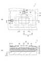
例えば、図16に示すような、半導体基板110上に酸化膜111、窒化膜112が形成され、その上にMEMS構造体が形成されたMEMSデバイスが知られている。このMEMSデバイスには固定電極と可動電極を備え、固定電極として入力側電極113、出力側電極114、駆動電極115、可動電極として入力側電極113に接続された可動部116が設けられている。
このような構造のMEMSデバイスでは、入力側電極113から出力側電極114へ半導体基板110の表面を介して高周波信号が漏洩することがある。
このことを解決するために、特許文献1には、振動子素子(MEMS構造体)の下部電極をまとめて共通に接続することにより、高周波信号配線の占める基板上の面積を少なくし、高周波信号の基板への漏洩量を低減する内容が開示されている。For example, as shown in FIG. 16, a MEMS device in which an
In the MEMS device having such a structure, a high frequency signal may leak from the
In order to solve this problem,
しかしながら、上記のようにMEMS構造体の占有面積を削減することは、寄生容量を低減させる有効な方法であるが、設計上・製造上の制約により占有面積の削減が困難な場合がある。このため、MEMS構造体の占有面積を削減できない場合には、寄生容量に起因するMEMSデバイスの特性への弊害が生じている。
本発明は、上記課題を解決するために成されたものであり、その目的は、MEMS構造体と半導体基板との間の寄生容量を低減させるMEMSデバイスを提供することにある。However, reducing the occupied area of the MEMS structure as described above is an effective method for reducing the parasitic capacitance, but it may be difficult to reduce the occupied area due to design and manufacturing restrictions. For this reason, when the occupation area of the MEMS structure cannot be reduced, there is an adverse effect on the characteristics of the MEMS device due to the parasitic capacitance.
The present invention has been made to solve the above-described problems, and an object thereof is to provide a MEMS device that reduces the parasitic capacitance between the MEMS structure and the semiconductor substrate.
上記課題を解決するために、本発明のMEMSデバイスは、半導体基板上に絶縁層を介して形成された固定電極と可動電極とを有するMEMS構造体が備えられたMEMSデバイスであって、前記固定電極の下方の前記半導体基板にウェルが形成されており、前記固定電極に正の電圧が印加される場合には前記ウェルがp型ウェルであり、前記固定電極に負の電圧が印加される場合には前記ウェルがn型ウェルであることを特徴とする。 In order to solve the above-described problems, a MEMS device according to the present invention is a MEMS device including a MEMS structure having a fixed electrode and a movable electrode formed on a semiconductor substrate via an insulating layer, When a well is formed in the semiconductor substrate below the electrode, and a positive voltage is applied to the fixed electrode, the well is a p-type well, and a negative voltage is applied to the fixed electrode The well is an n-type well.
この構成によれば、MEMS構造体における固定電極の下方の半導体基板にウェルが形成され、MEMS構造体の固定電極に正の電圧が印加される場合にはウェルがp型ウェルで、MEMS構造体の固定電極に負の電圧が印加される場合にはウェルがn型ウェルとしている。
このように、ウェルを形成することでウェルを形成した半導体基板表面が空乏状態となり、空乏層により見かけ上の対向電極間距離が増すため、この部分の寄生容量が減少する。よって、MEMS構造体と半導体基板との間の寄生容量を低減させることができ、半導体基板の表面を介して高周波信号が漏洩することがなくなり、MEMSデバイスの特性を安定化することができる。According to this configuration, the well is formed in the semiconductor substrate below the fixed electrode in the MEMS structure, and when a positive voltage is applied to the fixed electrode of the MEMS structure, the well is a p-type well, and the MEMS structure When a negative voltage is applied to the fixed electrode, the well is an n-type well.
Thus, by forming the well, the surface of the semiconductor substrate on which the well is formed is depleted, and the apparent distance between the counter electrodes is increased by the depletion layer, so that the parasitic capacitance of this portion is reduced. Therefore, the parasitic capacitance between the MEMS structure and the semiconductor substrate can be reduced, and a high frequency signal does not leak through the surface of the semiconductor substrate, and the characteristics of the MEMS device can be stabilized.
また、上記本発明のMEMSデバイスにおいて、前記ウェルが空乏状態となるように前記ウェルに電圧が印加されていることが望ましい。 In the MEMS device of the present invention, it is desirable that a voltage is applied to the well so that the well is depleted.
この構成によれば、固定電極の下方の半導体基板に形成されたウェルが空乏状態となるようにウェルに電圧が印加されている。
固定電極に絶対値で大きな電圧を印加したときにウェルの半導体基板表面に反転層が生じ電子が励起される。この状態では空乏容量によらず、半導体基板表面での信号漏洩が生じやすくなる。このため、固定電極に印加される電圧からウェルが空乏状態となる電圧を引いた値の電圧をウェルに印加すれば、ウェルは空乏状態を維持することができ、ウェルの半導体基板表面に反転層が生じ電子が励起されることを防止することができる。
このように、ウェルが空乏状態を維持することができるので、MEMS構造体と半導体基板との間の寄生容量を低減させることができ、半導体基板の表面を介して高周波信号が漏洩することがなくなり、MEMSデバイスの特性を安定化することができる。According to this configuration, a voltage is applied to the well so that the well formed in the semiconductor substrate below the fixed electrode is depleted.
When a voltage having a large absolute value is applied to the fixed electrode, an inversion layer is generated on the surface of the semiconductor substrate in the well and electrons are excited. In this state, signal leakage on the surface of the semiconductor substrate tends to occur regardless of the depletion capacity. Therefore, if a voltage having a value obtained by subtracting a voltage at which the well is depleted from the voltage applied to the fixed electrode is applied to the well, the well can maintain the depletion state, and the inversion layer is formed on the surface of the semiconductor substrate of the well. It is possible to prevent the electrons from being excited and excited.
As described above, since the well can maintain a depletion state, the parasitic capacitance between the MEMS structure and the semiconductor substrate can be reduced, and a high-frequency signal does not leak through the surface of the semiconductor substrate. The characteristics of the MEMS device can be stabilized.
また、本発明のMEMSデバイスにおいて、前記半導体基板がp型基板で前記ウェルがn型ウェルであって、前記MEMS構造体のバイアス電圧をVp、前記MEMS構造体の下方の前記ウェルに印加する電圧をVwell、前記ウェルに反転層が生ずるしきい値電圧をVth、としたとき、Vp<0、Vwell≧0、かつ、0<|Vp−Vwell|<|Vth|、を満足することが望ましい。 In the MEMS device of the present invention, the semiconductor substrate is a p-type substrate and the well is an n-type well, and the bias voltage of the MEMS structure is Vp, and the voltage applied to the well below the MEMS structure Is Vwell, and the threshold voltage at which the inversion layer is generated in the well is Vth, it is desirable that Vp <0, Vwell ≧ 0, and 0 <| Vp−Vwell | <| Vth |.
このように上記の条件を満足することで、半導体基板がp型基板でウェルがn型ウェルの場合に、固定電極の下方の半導体基板に形成されたウェルが空乏状態となる。そして、ウェルに生じた空乏層により見かけ上の対向電極間距離が増すため、この部分の寄生容量が減少する。よって、MEMS構造体と半導体基板との間の寄生容量を低減させることができ、半導体基板の表面を介して高周波信号が漏洩することがなくなり、MEMSデバイスの特性を安定化することができる。 By satisfying the above conditions as described above, when the semiconductor substrate is a p-type substrate and the well is an n-type well, the well formed in the semiconductor substrate below the fixed electrode is depleted. Further, since the apparent distance between the counter electrodes is increased by the depletion layer generated in the well, the parasitic capacitance in this portion is reduced. Therefore, the parasitic capacitance between the MEMS structure and the semiconductor substrate can be reduced, and a high frequency signal does not leak through the surface of the semiconductor substrate, and the characteristics of the MEMS device can be stabilized.
また、本発明のMEMSデバイスにおいて、前記半導体基板がn型基板で前記ウェルがp型ウェルであって、前記MEMS構造体のバイアス電圧をVp、前記MEMS構造体の下方の前記ウェルに印加する電圧をVwell、前記ウェルに反転層が生ずるしきい値電圧をVth、としたとき、Vp>0、Vwell≦0、かつ、0<|Vp−Vwell|<|Vth|、を満足することが望ましい。 In the MEMS device of the present invention, the semiconductor substrate is an n-type substrate and the well is a p-type well, the bias voltage of the MEMS structure is Vp, and the voltage applied to the well below the MEMS structure Is Vwell, and the threshold voltage at which the inversion layer is generated in the well is Vth, it is desirable that Vp> 0, Vwell ≦ 0, and 0 <| Vp−Vwell | <| Vth |.
このように上記の条件を満足することで、半導体基板がn型基板でウェルがp型ウェルの場合に、固定電極の下方の半導体基板に形成されたウェルが空乏状態となる。そして、ウェルに生じた空乏層により見かけ上の対向電極間距離が増すため、この部分の寄生容量が減少する。よって、MEMS構造体と半導体基板との間の寄生容量を低減させることができ、半導体基板の表面を介して高周波信号が漏洩することがなくなり、MEMSデバイスの特性を安定化することができる。 By satisfying the above conditions as described above, when the semiconductor substrate is an n-type substrate and the well is a p-type well, the well formed in the semiconductor substrate below the fixed electrode is depleted. Further, since the apparent distance between the counter electrodes is increased by the depletion layer generated in the well, the parasitic capacitance in this portion is reduced. Therefore, the parasitic capacitance between the MEMS structure and the semiconductor substrate can be reduced, and a high frequency signal does not leak through the surface of the semiconductor substrate, and the characteristics of the MEMS device can be stabilized.
また、上記本発明のMEMSデバイスにおいて、半導体基板上に絶縁層を介して形成された固定電極と可動電極とを有するMEMS構造体が備えられたMEMSデバイスであって、前記固定電極の下方の前記半導体基板に前記半導体基板と同極性のウェルが形成されており、前記半導体基板内にて前記ウェルを取り囲み、前記ウェルと逆極性を有する分離用ウェルが形成され、前記ウェルと前記分離用ウェルの間、または前記分離用ウェルと前記半導体基板の間が逆バイアスになるように構成されていることを特徴とする。 In the MEMS device of the present invention, the MEMS device includes a MEMS structure having a fixed electrode and a movable electrode formed on a semiconductor substrate via an insulating layer, the MEMS device being provided below the fixed electrode. A well having the same polarity as that of the semiconductor substrate is formed in the semiconductor substrate, and a separation well is formed that surrounds the well in the semiconductor substrate and has a polarity opposite to that of the well. Or between the separation well and the semiconductor substrate so as to have a reverse bias.
この構成によれば、半導体基板とウェルの電位を切り離すことができ、絶対値において高い電圧でMEMS構造体を稼動させることが可能となり、MEMS構造体と半導体基板との間の寄生容量を低減させることができる。また、このような構成を採用すれば、ウェルの電位が半導体基板の電位に影響を与えないことから、MEMS構造体とICなどの回路とを一体化して利用することが容易となる。 According to this configuration, the potential of the semiconductor substrate and the well can be separated, the MEMS structure can be operated at a high voltage in absolute value, and the parasitic capacitance between the MEMS structure and the semiconductor substrate is reduced. be able to. Further, if such a configuration is adopted, the potential of the well does not affect the potential of the semiconductor substrate, so that the MEMS structure and a circuit such as an IC can be used in an integrated manner.
また、本発明のMEMSデバイスにおいて、前記半導体基板がp型基板で前記ウェルがp型ウェル、前記分離用ウェルがn型ウェルであって、前記MEMS構造体のバイアス電圧をVp、前記MEMS構造体の下方の前記ウェルに印加する電圧をVwell、前記ウェルに反転層が生ずるしきい値電圧をVth、としたとき、Vp>0、かつ、0<Vp−Vwell<Vth、を満足することが望ましい。 In the MEMS device of the present invention, the semiconductor substrate is a p-type substrate, the well is a p-type well, and the separation well is an n-type well, and the bias voltage of the MEMS structure is Vp, and the MEMS structure It is preferable that Vp> 0 and 0 <Vp−Vwell <Vth are satisfied, where Vwell is a voltage applied to the well below V and Vth is a threshold voltage at which an inversion layer is generated in the well. .
このように上記の条件を満足することで、半導体基板がp型基板でウェルがp型ウェル、分離用ウェルがn型ウェルの場合に、固定電極の下方の半導体基板に形成されたウェルが空乏状態となる。そして、ウェルに生じた空乏層により見かけ上の対向電極間距離が増すため、この部分の寄生容量が減少する。よって、MEMS構造体と半導体基板との間の寄生容量を低減させることができ、半導体基板の表面を介して高周波信号が漏洩することがなくなり、MEMSデバイスの特性を安定化することができる。 By satisfying the above conditions as described above, when the semiconductor substrate is a p-type substrate, the well is a p-type well, and the separation well is an n-type well, the well formed in the semiconductor substrate below the fixed electrode is depleted. It becomes a state. Further, since the apparent distance between the counter electrodes is increased by the depletion layer generated in the well, the parasitic capacitance in this portion is reduced. Therefore, the parasitic capacitance between the MEMS structure and the semiconductor substrate can be reduced, and a high frequency signal does not leak through the surface of the semiconductor substrate, and the characteristics of the MEMS device can be stabilized.
また、本発明のMEMSデバイスにおいて、前記半導体基板がn型基板で前記ウェルがn型ウェル、前記分離用ウェルがp型ウェルであって、前記MEMS構造体のバイアス電圧をVp、前記MEMS構造体の下方の前記ウェルに印加する電圧をVwell、前記ウェルに反転層が生ずるしきい値電圧をVth、としたとき、Vp<0、かつ、0<Vp−Vwell<Vth、を満足することが望ましい。 In the MEMS device of the present invention, the semiconductor substrate is an n-type substrate, the well is an n-type well, and the separation well is a p-type well, and the bias voltage of the MEMS structure is Vp, and the MEMS structure It is preferable that Vp <0 and 0 <Vp−Vwell <Vth are satisfied, where Vwell is a voltage applied to the well below and Vth is a threshold voltage at which an inversion layer is generated in the well. .
このように上記の条件を満足することで、半導体基板がn型基板でウェルがn型ウェル、分離用ウェルがp型ウェルの場合に、固定電極の下方の半導体基板に形成されたウェルが空乏状態となる。そして、ウェルに生じた空乏層により見かけ上の対向電極間距離が増すため、この部分の寄生容量が減少する。よって、MEMS構造体と半導体基板との間の寄生容量を低減させることができ、半導体基板の表面を介して高周波信号が漏洩することがなくなり、MEMSデバイスの特性を安定化することができる。 By satisfying the above conditions as described above, when the semiconductor substrate is an n-type substrate, the well is an n-type well, and the separation well is a p-type well, the well formed in the semiconductor substrate below the fixed electrode is depleted. It becomes a state. Further, since the apparent distance between the counter electrodes is increased by the depletion layer generated in the well, the parasitic capacitance in this portion is reduced. Therefore, the parasitic capacitance between the MEMS structure and the semiconductor substrate can be reduced, and a high frequency signal does not leak through the surface of the semiconductor substrate, and the characteristics of the MEMS device can be stabilized.
本発明の実施形態の説明に先立ち、発明の理解のために半導体基板に寄生容量が生じて信号が本来の経路以外からリークする原理について説明する。
まず、半導体に絶縁体を介して金属が形成されたキャパシタをモデルとして上記の現象を解説することができ、p型半導体を用いたMOSキャパシタを例にとり説明する。
p型半導体を用いたMOSキャパシタの容量−電圧特性において、ゲート電圧が負の場合には蓄積状態、ゲート電圧に正の電圧を加えた場合には空乏状態、ゲートに大きな正の電圧を加えた場合には反転状態となることが知られている。
蓄積状態では、基板表面にキャリア(正孔)が生じ基板表面付近の導体抵抗が下がり、横方向への信号漏洩が発生しやすくなる。
また空乏状態では、見かけ上の対向電極間距離が増すため、この部分の寄生容量が減少し、基板表面付近にはキャリアが生じず、横方向への信号漏洩が起こりにくくなる。
さらに反転状態では、基板表面に反転層が生じ、ここに反対の符号を持ったキャリアが励起され、基板表面で横方向への信号漏洩が発生しやすくなる。Prior to the description of the embodiments of the present invention, for the understanding of the present invention, the principle that a parasitic capacitance occurs in a semiconductor substrate and a signal leaks from other than the original path will be described.
First, the above phenomenon can be explained using a capacitor in which a metal is formed on a semiconductor via an insulator as a model. A MOS capacitor using a p-type semiconductor will be described as an example.
In the capacitance-voltage characteristics of a MOS capacitor using a p-type semiconductor, an accumulation state is applied when the gate voltage is negative, a depletion state is applied when a positive voltage is applied to the gate voltage, and a large positive voltage is applied to the gate. In some cases, it is known to be in an inverted state.
In the accumulation state, carriers (holes) are generated on the substrate surface, the conductor resistance near the substrate surface is lowered, and signal leakage in the lateral direction is likely to occur.
Further, in the depletion state, the apparent distance between the counter electrodes is increased, so that the parasitic capacitance in this portion is reduced, carriers are not generated in the vicinity of the substrate surface, and signal leakage in the lateral direction is less likely to occur.
Further, in the inversion state, an inversion layer is formed on the substrate surface, and carriers having opposite signs are excited here, and signal leakage in the lateral direction is likely to occur on the substrate surface.
このように、空乏状態では、基板表面で横方向への信号漏洩が生じにくい。そして、MEMSデバイスは一般に高い電圧で動作するため、反転層が生ずる電圧(しきい値電圧)値が高いほど基板表面での信号漏洩が起きにくくなる。
また、半導体基板にウェルが形成されていると、基板表面に電圧を印加した場合により高い印加電圧まで反転層が生じにくくなる。
MOSキャパシタにおける反転層が生ずる電圧はMOSトランジスタのしきい値電圧導出式で表すことができる。p型ウェルを用いた場合のしきい値電圧Vtを式(1)に示す。Thus, in the depletion state, signal leakage in the lateral direction hardly occurs on the substrate surface. Since the MEMS device generally operates at a high voltage, the higher the voltage (threshold voltage) value generated by the inversion layer is, the less likely signal leakage occurs on the substrate surface.
In addition, when a well is formed in a semiconductor substrate, an inversion layer is less likely to be generated up to a higher applied voltage when a voltage is applied to the substrate surface.
The voltage generated by the inversion layer in the MOS capacitor can be expressed by a threshold voltage derivation formula of the MOS transistor. The threshold voltage Vt when a p-type well is used is shown in equation (1).

k:ボルツマン定数
T:温度
q:電荷の絶対値
NA:アクセプタ濃度
ni:真性キャリア濃度
Ci:絶縁膜の単位面積あたりの容量
ε0:真空中の誘電率
εS:絶縁膜の比誘電率
この式によれば、反転が始まるしきい値電圧は半導体基板部分のアクセプタ濃度に依存することがわかる。アクセプタ濃度はウェルのキャリア濃度でほぼ近似できることから、キャリア濃度が大きいほど、高い電圧までMOSキャパシタが空乏状態を維持することが可能であるのがわかる。
またウェルを形成せずにp型シリコン基板をそのまま使用した場合について考えると、基板のキャリア濃度がウェル形成時よりも小さくなるために、式(1)によれば反転層が生ずる電圧が低くなり、空乏状態で使用できる電圧範囲が狭くなることが理解できる。
この様に、ウェルを形成することで、より広い電圧範囲でMEMSデバイスへの寄生容量の削減が可能となる。
さらに、ウェルを形成する場合は用いる基板種類(p型基板若しくはn型基板)によらず最適な基板構造をMEMS構造体の固定電極下方に設けることが可能であり、用いる基板種類によらず寄生容量の抑圧が可能となる。
k: Boltzmann constant T: temperature q: absolute value of charge NA : acceptor concentration ni : intrinsic carrier concentration Ci : capacitance per unit area of insulating film ε0 : dielectric constant in vacuum εS : ratio of insulating film Dielectric constant According to this equation, it can be seen that the threshold voltage at which inversion begins depends on the acceptor concentration of the semiconductor substrate portion. Since the acceptor concentration can be approximated by the carrier concentration of the well, it can be seen that the higher the carrier concentration, the more the MOS capacitor can be kept in a depletion state.
Considering the case where a p-type silicon substrate is used as it is without forming a well, the carrier concentration of the substrate is smaller than that at the time of forming the well, so that the voltage generated by the inversion layer is reduced according to equation (1). It can be understood that the voltage range that can be used in the depletion state becomes narrow.
In this way, by forming the well, it is possible to reduce the parasitic capacitance to the MEMS device in a wider voltage range.
Further, when forming a well, an optimum substrate structure can be provided below the fixed electrode of the MEMS structure regardless of the substrate type (p-type substrate or n-type substrate) to be used. Capacity suppression is possible.
以上のように、半導体基板にウェルを形成することで、反転層の発生電圧を引き上げ、基板表面の信号漏洩を抑圧することができる。
なお、n型半導体基板においても、ゲート電圧により蓄積状態、空乏状態、反転状態を生ずることが知られており、上記と同様に、空乏状態を利用することで寄生容量が減少し、基板表面付近にはキャリアが生じず、横方向への信号漏洩が起こりにくくなる。As described above, by forming a well in the semiconductor substrate, the voltage generated in the inversion layer can be increased and signal leakage on the substrate surface can be suppressed.
In addition, it is known that an n-type semiconductor substrate causes an accumulation state, a depletion state, and an inversion state by a gate voltage. As in the above, parasitic capacitance is reduced by using the depletion state, and the vicinity of the substrate surface No carrier is generated, and signal leakage in the lateral direction is less likely to occur.
次に、MEMS構造体の固定電極下方を空乏状態で動作させた場合の具体的なデバイスの特性について述べる。ここでは、一例としてMEMS振動子へ適用した場合の効果について説明する。
上記の様に半導体基板を空乏状態でMEMS振動子を動作させた場合、形成される寄生容量値が減少することから、これら寄生容量を介して通過する信号分が減少するため、共振ピークが急峻となる。
また、能動回路と接続して発振回路を構成する場合、MEMS振動子に含まれる寄生容量は等価的にトランジスタに含まれる寄生容量として見なされることから、トランジスタにより生成可能な負性抵抗が減少することが知られている。従って、MEMS振動子の寄生容量が減少すれば、トランジスタの能力に対して生成可能な負性抵抗値が増大するため、回路の低消費電力化が可能となる。
一方でウェルを構成しない場合は、MEMS振動子へ印加可能なバイアス電圧が低下する。MEMS振動子にしきい値以上のバイアス電圧を印加した場合は、MEMS構造体の固定電極下方の基板が反転状態となるため、基板表面に少数キャリアである電子が励起され、横方向へ信号が流れやすくなる。また、固定電極と基板との間の寄生容量も併せて増大することから、等価的にMEMS振動子の寄生容量が増大する。この結果、振動子の共振ピークがなまる(Q値劣化)等の弊害が生ずる。
以上、MEMS構造体の固定電極下方の基板を空乏状態で使用することにより、MEMS構造体の電気特性を改善できることを説明した。
以下、本発明を具体化した実施形態について図面に従って説明する。
(第1の実施形態)Next, specific device characteristics when the MEMS structure is operated in a depleted state below the fixed electrode will be described. Here, the effect when applied to a MEMS vibrator will be described as an example.
When the MEMS vibrator is operated with the semiconductor substrate being depleted as described above, the parasitic capacitance value formed decreases, and therefore, the amount of signals passing through these parasitic capacitances decreases, so the resonance peak is steep. It becomes.
Further, when the oscillation circuit is configured by connecting to the active circuit, the parasitic capacitance included in the MEMS vibrator is equivalently regarded as the parasitic capacitance included in the transistor, and thus the negative resistance that can be generated by the transistor is reduced. It is known. Therefore, if the parasitic capacitance of the MEMS vibrator is reduced, the negative resistance value that can be generated with respect to the capability of the transistor is increased, so that the power consumption of the circuit can be reduced.
On the other hand, when the well is not configured, the bias voltage that can be applied to the MEMS vibrator decreases. When a bias voltage higher than a threshold value is applied to the MEMS vibrator, the substrate under the fixed electrode of the MEMS structure is in an inverted state, so that electrons that are minority carriers are excited on the substrate surface, and a signal flows in the lateral direction. It becomes easy. In addition, since the parasitic capacitance between the fixed electrode and the substrate also increases, the parasitic capacitance of the MEMS vibrator increases equivalently. As a result, problems such as the resonance peak of the vibrator becoming dull (Q value deterioration) occur.
As described above, it has been described that the electrical characteristics of the MEMS structure can be improved by using the substrate below the fixed electrode of the MEMS structure in a depleted state.
DESCRIPTION OF EXEMPLARY EMBODIMENTS Hereinafter, embodiments of the invention will be described with reference to the drawings.
(First embodiment)
図1は本実施形態のMEMSデバイスの構成を示し、図1(a)はMEMSデバイスの部分模式平面図、図1(b)は同図(a)のA−A断線に沿う部分模式断面図である。 FIG. 1 shows the configuration of the MEMS device of the present embodiment, FIG. 1A is a partial schematic plan view of the MEMS device, and FIG. 1B is a partial schematic cross-sectional view taken along the line AA in FIG. It is.
MEMSデバイス1は、半導体基板10にMEMS構造体30、MEMS構造体30を取り囲むように形成された配線層27、配線層27の上方からMEMS構造体30上方に連なり開口部29が形成されたパッシベーション膜28を備えている。
シリコンからなるp型の半導体基板10上にはシリコン酸化膜11が形成され、その上にシリコン窒化膜12が形成されている。そして、シリコン窒化膜12上にMEMS構造体30が設けられている。MEMS構造体30は、ポリシリコンにて形成され、固定電極20と可動電極26を有している。固定電極20はシリコン窒化膜12上に配置され、入力側電極21a,21b、出力側電極22を備えている。可動電極26は、入力側電極21a,21bから立ち上がった部分を保持されることで、両持ち状態で空中に保持されている。The
A
入力側電極21aの一端は、MEMS構造体30を取り囲む配線層27に延出し、配線31に接続されている。配線層27は、SiO2になどの絶縁膜が積層され、配線層27を経由した配線31は、その上部に設けられた接続パッドからアルミ配線32に接続されている。
また、出力側電極22の一端は、MEMS構造体30を取り囲む配線層27に延出し、配線33に接続され、さらに配線層27の上部に設けられた接続パッドからアルミ配線34に接続されている。
なお、配線層27の下にはSiO2などの酸化膜24が形成されており、MEMS構造体30をエッチングにてリリースする際の犠牲層である。One end of the input-
Further, one end of the
An
また、MEMS構造体30における固定電極である入力側電極21a,21b、出力側電極22の下方の半導体基板10には、p型のウェル13が形成されている。このウェル13は、平面視でMEMS構造体30を含む領域に形成されている。 A p-
そして、配線層27の上からMEMS構造体30上方に連なってパッシベーション膜28が形成されている。パッシベーション膜28には開口部29が形成され、この開口部29から配線層27、酸化膜24をエッチングすることでMEMS構造体30をリリースし、パッシベーション膜28と半導体基板10の間に、MEMS構造体30を配置する空洞部35が画定されている。なお、ウェル13には固定の電圧が印加されている。 A
このような構造のMEMSデバイス1は、MEMS構造体30の入力側電極21aを介して可動電極26に直流電圧が印加されると、可動電極26と出力側電極22の間に電位差が生じ、可動電極26と出力側電極22の間に静電力が働く。ここで、さらに可動電極26に交流電圧が印加されると、静電力が大きくなったり小さくなったり変動し、可動電極26が出力側電極22に近づいたり、遠ざかる方向に振動する。このとき、出力側電極22の電極表面では、電荷の移動が生じ、出力側電極22に電流が流れる。そして、振動が繰り返されることから、出力側電極22から固有の共振周波数信号が出力される。
MEMS構造体30に印加される電圧がウェルの反転電圧以下である場合は、ウェル13は接地して使用する。
一方で、MEMS構造体30への印加電圧が上記ウェルの反転電圧以上である場合はウェル13には空乏状態を維持できる電圧を印加して使用する。
例えば、MEMS構造体30の駆動電圧が8V、ウェル13に反転層が発生する電位が7Vのとき、ウェル13に3Vの電圧が印加されることで、ウェル13とMEMS構造体30の間の電位差は5Vとなり、半導体基板10のウェル13は反転層が発生せず空乏状態を維持している。この場合、ウェル13周辺には逆の極性を有するウェル(n型ウェル)をガードリングとして構成(図示せず)し、絶対値がウェル13に印加される電圧値以上で、ウェル13と同極性の電圧を印加して使用する。例えばウェル13に3V印加する場合は、周辺のガードリング部には5Vを印加して使用する。In the
When the voltage applied to the
On the other hand, when the voltage applied to the
For example, when the drive voltage of the
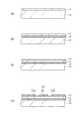
次に、上記構成のMEMSデバイスの製造方法について説明する。
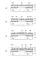
図2、図3、図4はMEMSデバイスの製造方法を示す模式部分断面図である。
まず図2(a)に示すように、シリコンからなる半導体基板10の上に熱酸化によりシリコン酸化膜11を形成する。次に、図2(b)に示すように、所定領域にBイオンを半導体基板10にイオン注入してp型のウェル13を形成する。続いて、図2(c)に示すように、シリコン酸化膜11の上にシリコン窒化膜12を形成する。そして、図2(d)に示すように、シリコン窒化膜12の上にポリシリコン膜を形成し、パターニングによりMEMS構造体の固定電極20である入力側電極21a,21b、出力側電極22を形成する。Next, a manufacturing method of the MEMS device having the above configuration will be described.
2, 3 and 4 are schematic partial cross-sectional views showing a method for manufacturing a MEMS device.
First, as shown in FIG. 2A, a
次に、図3(a)に示すように、入力側電極21a,21b、出力側電極22の上からSiO2などの酸化膜24を形成する。その後、図3(b)に示すように、入力側電極21a,21b上の酸化膜24に開口穴25を形成する。続いて、酸化膜24の上にポリシリコン膜を形成し、パターニングを行い、図3(c)に示すように、エッチングによりMEMS構造体の可動電極26を形成する。そして、図3(d)に示すように、SiO2などの絶縁膜を介して配線(図示せず)を積層した配線層27を形成する。Next, as shown in FIG. 3A, an
次に、図4(a)に示すように、配線層27の上にパッシベーション膜28を形成する。続いて、図4(b)に示すように、MEMS構造体の上方のパッシベーション膜28に開口部29を形成する。
そして、図4(c)に示すように、開口部29から酸性のエッチング液を接触させて、配線層27、酸化膜24をエッチングしてMEMS構造体30をリリースする。このとき、半導体基板10とパッシベーション膜28との間に空洞部35が形成されている。このようにして図1に示すようなMEMSデバイス1が製造される。Next, as shown in FIG. 4A, a
Then, as shown in FIG. 4C, an acidic etching solution is contacted from the
以上のように、本実施形態のMEMSデバイス1は、MEMS構造体30における固定電極20の下方にウェル13が形成され、MEMS構造体30の固定電極20に正の電圧が印加され、ウェル13がp型のウェルで構成されている。さらに、固定電極20の下方の半導体基板10に形成されたウェル13が空乏状態となるようにウェル13に固定の電圧が印加されている。
このように、ウェル13を形成しウェル13が空乏状態となるようにウェル13に固定の電圧を印加することで半導体基板1表面が空乏状態となり、空乏層により見かけ上の対向電極間距離が増すため、この部分の寄生容量が減少する。よって、MEMS構造体30と半導体基板10との間の寄生容量を低減させ、半導体基板10の表面を介しての高周波信号漏洩を削減することができ、MEMSデバイス1の特性が安定化する。
(変形例1)As described above, in the
Thus, by forming a well 13 and applying a fixed voltage to the well 13 so that the well 13 is depleted, the surface of the
(Modification 1)
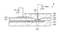
次に、実施形態1における半導体基板およびウェルの極性の組合せによる変形例について説明する。本変形例1では半導体基板がp型基板で、ウェルがn型ウェルの場合である。また、半導体基板には回路素子が形成され、半導体基板の電位は一般的な0Vに設定されている。
図5は変形例1におけるMEMSデバイスの構成を示す部分模式断面図である。
MEMSデバイス5は、半導体基板120にMEMS構造体(ここではMEMS構造体の可動電極は省略し固定電極の入力側電極131のみ示している)と、MEMS構造体の回りに形成された配線層127、配線層127の上方に形成されたパッシベーション膜128とを備えている。
シリコンからなるp型の半導体基板120上にはシリコン酸化膜121が形成され、その上にシリコン窒化膜122が形成されている。そして、シリコン窒化膜122上にMEMS構造体が設けられている。MEMS構造体は、図1で説明したMEMS構造体と同様の構造であり、詳細な説明は省略する。Next, a modified example of the combination of the polarities of the semiconductor substrate and the well in the first embodiment will be described. In the first modification, the semiconductor substrate is a p-type substrate and the well is an n-type well. Further, circuit elements are formed on the semiconductor substrate, and the potential of the semiconductor substrate is set to a general 0V.
FIG. 5 is a partial schematic cross-sectional view showing the configuration of the MEMS device according to the first modification.
The
A
MEMS構造体における固定電極である入力側電極131の下方の半導体基板120には、n型のウェル123が形成されている。このウェル123は、平面視でMEMS構造体を含む領域に形成されている。
また、ウェル123の一部には電極125が形成され、電極125は配線126により配線層127を経てパッシベーション膜128の上面まで接続されている。
そして、ウェル123は配線126を介して正の電圧が印加されている。また、MEMS構造体の入力側電極131は負の電圧が印加されている。An n-
In addition, an
A positive voltage is applied to the well 123 via the
ここで、ウェル123に反転層が生ずるしきい値電圧をVth、MEMS構造体に印加するバイアス電圧をVp、MEMS構造体の下方のウェル123に印加する電圧をVwell、とする。
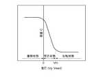
このような状態におけるVpとVwellとの差(Vp−Vwell)とMEMS構造体とウェル間の容量Cとの関係を示すグラフを図6に示す。
半導体基板120がp型基板で、ウェル123がn型ウェルの場合、しきい値電圧Vth<0である。Vp−Vwellの電圧が正の場合には、ウェルは蓄積状態であり、MEMS構造体とウェル間の容量Cは大きい値であり寄生容量が大きいことになる。Vp−Vwellの電圧が0からしきい値電圧Vthの間が、ウェルが空乏状態となる範囲であり、MEMS構造体とウェル間の容量Cは0Vからしきい値電圧Vthに向かうに従って小さくなり寄生容量も小さくなる。そして、しきい値電圧Vthより小さくなるとウェルが反転状態となる。前述したように、ウェルを空乏状態で使用することでMEMS構造体と半導体基板間の寄生容量を減少させることができ、また、基板表面付近で横方向への信号漏洩が起こりにくくすることができる。
このウェルを空乏状態とするためには、Vp<0、Vwell≧0、かつ、0<|Vp−Vwell|<|Vth|となる条件を満足することが必要である。Here, a threshold voltage at which an inversion layer is generated in the well 123 is Vth, a bias voltage applied to the MEMS structure is Vp, and a voltage applied to the well 123 below the MEMS structure is Vwell.
FIG. 6 is a graph showing the relationship between the difference between Vp and Vwell (Vp−Vwell) and the capacitance C between the MEMS structure and the well in such a state.
When the
In order to make this well depleted, it is necessary to satisfy the conditions of Vp <0, Vwell ≧ 0, and 0 <| Vp−Vwell | <| Vth |.
以上のように、上記の条件を満足することで、半導体基板120がp型基板でウェル123がn型ウェルの場合に、固定電極の下方の半導体基板120に形成されたウェル123が空乏状態となる。そして、ウェル123に生じた空乏層により見かけ上の対向電極間距離が増すため、この部分の寄生容量が減少する。よって、MEMS構造体と半導体基板120との間の寄生容量を低減させることができ、半導体基板120の表面を介して高周波信号が漏洩することがなくなり、MEMSデバイス5の特性を安定化することができる。そして、このような構成を採用すれば、MEMS構造体とICなどの回路とを一体化して利用することが容易となる。
(変形例2)As described above, when the above conditions are satisfied, when the
(Modification 2)
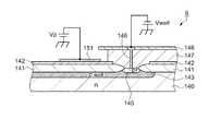
次に、実施形態1における半導体基板およびウェルの極性の組合せによる他の変形例について説明する。本変形例2では半導体基板がn型基板で、ウェルがp型ウェルの場合である。また、半導体基板には回路素子が形成され、半導体基板の電位は一般的な0Vに設定されている。
図7は変形例2におけるMEMSデバイスの構成を示す部分模式断面図である。
MEMSデバイス6は、半導体基板140にMEMS構造体(ここではMEMS構造体の可動電極は省略し固定電極の入力側電極151のみ示している)と、MEMS構造体の回りに形成された配線層147、配線層147の上方に形成されたパッシベーション膜148とを備えている。
シリコンからなるn型の半導体基板140上にはシリコン酸化膜141が形成され、その上にシリコン窒化膜142が形成されている。そして、シリコン窒化膜142上にMEMS構造体が設けられている。MEMS構造体は、図1で説明したMEMS構造体と同様の構造であり、詳細な説明は省略する。Next, another modification example according to the combination of the polarities of the semiconductor substrate and the well in the first embodiment will be described. In the second modification, the semiconductor substrate is an n-type substrate and the well is a p-type well. Further, circuit elements are formed on the semiconductor substrate, and the potential of the semiconductor substrate is set to a general 0V.
FIG. 7 is a partial schematic cross-sectional view showing the configuration of the MEMS device in
The MEMS device 6 includes a MEMS structure on the semiconductor substrate 140 (here, the movable electrode of the MEMS structure is omitted and only the
A
MEMS構造体における固定電極である入力側電極151の下方の半導体基板140には、p型のウェル143が形成されている。このウェル143は、平面視でMEMS構造体を含む領域に形成されている。
また、ウェル143の一部には電極145が形成され、電極145は配線146により配線層147を経てパッシベーション膜148の上面まで接続されている。
そして、ウェル143は配線146を介して負の電圧が印加されている。また、MEMS構造体の入力側電極151は正の電圧が印加されている。A p-
An
A negative voltage is applied to the well 143 through the
ここで、ウェル143に反転層が生ずるしきい値電圧をVth、MEMS構造体に印加するバイアス電圧をVp、MEMS構造体の下方のウェル143に印加する電圧をVwell、とする。
このような状態におけるVpとVwellとの差(Vp−Vwell)とMEMS構造体とウェル間の容量Cとの関係を示すグラフを図8に示す。
半導体基板140がn型基板で、ウェル143がp型ウェルの場合、しきい値電圧Vth>0である。Vp−Vwellの電圧が負の場合には、ウェルは蓄積状態であり、MEMS構造体とウェル間の容量Cは大きい値であり寄生容量が大きいことになる。Vp−Vwellの電圧が0からしきい値電圧Vthの間が、ウェルが空乏状態となる範囲であり、MEMS構造体とウェル間の容量Cは0Vからしきい値電圧Vthに向かうに従って小さくなり寄生容量も小さくなる。そして、しきい値電圧Vthより大きくなるとウェルが反転状態となる。前述したように、ウェルを空乏状態で使用することでMEMS構造体と半導体基板間の寄生容量を減少させることができ、また、基板表面付近で横方向への信号漏洩が起こりにくくすることができる。
このウェルを空乏状態とするためには、Vp>0、Vwell≦0、かつ、0<|Vp−Vwell|<|Vth|となる条件を満足することが必要である。Here, the threshold voltage at which the inversion layer is generated in the well 143 is Vth, the bias voltage applied to the MEMS structure is Vp, and the voltage applied to the well 143 below the MEMS structure is Vwell.
FIG. 8 is a graph showing the relationship between the difference between Vp and Vwell (Vp−Vwell) and the capacitance C between the MEMS structure and the well in such a state.
When the
In order to make this well depleted, it is necessary to satisfy the conditions of Vp> 0, Vwell ≦ 0, and 0 <| Vp−Vwell | <| Vth |.
以上のように、上記の条件を満足することで、半導体基板140がn型基板でウェル143がp型ウェルの場合に、固定電極の下方の半導体基板140に形成されたウェル143が空乏状態となる。そして、ウェル143に生じた空乏層により見かけ上の対向電極間距離が増すため、この部分の寄生容量が減少する。よって、MEMS構造体と半導体基板140との間の寄生容量を低減させることができ、半導体基板140の表面を介して高周波信号が漏洩することがなくなり、MEMSデバイス6の特性を安定化することができる。そして、このような構成を採用すれば、MEMS構造体とICなどの回路とを一体化して利用することが容易となる。
(第2の実施形態)As described above, by satisfying the above conditions, when the
(Second Embodiment)
次に、第2の実施形態におけるMEMSデバイスについて説明する。
本実施形態において、第1の実施形態と異なる点は、半導体基板に形成されるウェルが入力側電極と出力側電極でそれぞれ独立して設けられていることである。
図9は本実施形態のMEMSデバイスの構成を示し、図9(a)はMEMSデバイスの部分模式平面図、図9(b)は同図(a)のB−B断線に沿う部分模式断面図である。Next, a MEMS device according to the second embodiment will be described.
The present embodiment is different from the first embodiment in that wells formed in the semiconductor substrate are provided independently for the input side electrode and the output side electrode, respectively.
FIG. 9 shows the configuration of the MEMS device of the present embodiment, FIG. 9A is a partial schematic plan view of the MEMS device, and FIG. 9B is a partial schematic cross-sectional view taken along the line BB in FIG. It is.
MEMSデバイス2は、半導体基板10にMEMS構造体60、MEMS構造体60を取り囲むように形成された配線層57、配線層57の上方からMEMS構造体60上方に連なり開口部59が形成されたパッシベーション膜58を備えている。
シリコンからなるp型の半導体基板10上にはシリコン酸化膜11が形成され、その上にシリコン窒化膜12が形成されている。そして、シリコン窒化膜12上にMEMS構造体60が設けられている。MEMS構造体60は、ポリシリコンにて形成され、固定電極50と可動電極56を有している。固定電極50はシリコン窒化膜12上に配置され、入力側電極51a,51b、出力側電極52を備えている。可動電極56は、入力側電極51a,51bから立ち上がった部分を保持されることで、両持ち状態で空中に保持されている。The
A
入力側電極51aの一端は、MEMS構造体60を取り囲む配線層57に延出し、配線61に接続されている。配線層57は、SiO2などの絶縁膜が積層され、配線層57を経由した配線61は、その上部に設けられた接続パッドからアルミ配線62に接続されている。
また、出力側電極52の一端は配線層57に延出し、配線63に接続され、さらに配線層57の上部に設けられた接続パッドからアルミ配線64に接続されている。
なお、配線層57の下にはSiO2などの酸化膜54が形成されており、MEMS構造体60をエッチングにてリリースする際の犠牲層である。One end of the
Further, one end of the
An
また、MEMS構造体60における固定電極50である入力側電極51a,51bの下方の半導体基板10には、p型のウェル43a,43bがそれぞれ形成されている。
そして、配線層57の上からMEMS構造体60上方に連なってパッシベーション膜58が形成されている。パッシベーション膜58には開口部59が形成され、この開口部59から配線層57、酸化膜54をエッチングすることでMEMS構造体60をリリースし、パッシベーション膜58と半導体基板10の間に、MEMS構造体60を配置する空洞部65が画定されている。なお、ウェル43a,43bには固定の電圧がそれぞれ印加されている。In addition, p-
A
このような構造のMEMSデバイス2は、MEMS構造体60の入力側電極51aを介して可動電極56に直流電圧が印加されると、可動電極56と出力側電極52の間に電位差が生じ、可動電極56と出力側電極52の間に静電力が働く。ここで、さらに可動電極56に交流電圧が印加されると、静電力が大きくなったり小さくなったり変動し、可動電極56が出力側電極52に近づいたり、遠ざかる方向に振動する。このとき、出力側電極52の電極表面では、電荷の移動が生じ、出力側電極52に電流が流れる。そして、振動が繰り返されることから、出力側電極52から固有の共振周波数信号が出力される。
MEMS構造体60に印加される電圧がウェルの反転電圧以下である場合は、ウェル43a,43bは接地して使用する。
一方で、MEMS構造体60への印加電圧が上記ウェルの反転電圧以上である場合はウェル43a及びウェル43bには空乏状態を維持できる電圧を印加して使用する。
例えば、MEMS構造体60の駆動電圧が8V、半導体基板10に反転層が発生する電位が7Vのとき、ウェル43a,43bに3Vの電圧が印加されることで、半導体基板10とMEMS構造体60の間の電位差は5Vとなり、半導体基板10のウェル43a,43bは反転層が発生せず空乏状態を維持している。
この場合、ウェル43a,43b周辺には逆の極性を有するウェルをガードリングとして構成(図示せず)し、ウェル13以上の絶対値を有し、ウェル43a,43bと同極性の電圧を印加して使用する。例えばウェル43a,43bに3V印加する場合は、周辺のガードリング部には5Vを印加して使用する。In the
When the voltage applied to the
On the other hand, when the voltage applied to the
For example, when the drive voltage of the
In this case, a well having opposite polarity is formed around the
次に、上記構成のMEMS振動子の製造方法について説明する。
図10、図11、図12はMEMSデバイスの製造方法を示す模式部分断面図である。
まず図10(a)に示すように、シリコンからなる半導体基板10の上に熱酸化によりシリコン酸化膜11を形成する。次に、図10(b)に示すように、所定領域にBイオンを半導体基板10にイオン注入してp型のウェル43a,43bを形成する。続いて、図10(c)に示すように、シリコン酸化膜11の上にシリコン窒化膜12を形成する。そして、図10(d)に示すように、シリコン窒化膜12の上にポリシリコン膜を形成し、パターニングによりMEMS構造体の固定電極50である入力側電極51a,51b、出力側電極52を形成する。Next, a method for manufacturing the MEMS vibrator having the above configuration will be described.
10, FIG. 11 and FIG. 12 are schematic partial cross-sectional views showing a method for manufacturing a MEMS device.
First, as shown in FIG. 10A, a
次に、図11(a)に示すように、入力側電極51a,51b、出力側電極52の上からSiO2などの酸化膜54を形成する。その後、図11(b)に示すように、入力側電極51a,51b上の酸化膜54に開口穴55を形成する。続いて、酸化膜54の上にポリシリコン膜を形成し、パターニングを行い、図11(c)に示すように、エッチングによりMEMS構造体の可動電極56を形成する。そして、図11(d)に示すように、SiO2などの絶縁膜を介して配線(図示せず)を積層した配線層57を形成する。Next, as shown in FIG. 11A, an
次に、図12(a)に示すように、配線層57の上にパッシベーション膜58を形成する。続いて、図12(b)に示すように、MEMS構造体の上方のパッシベーション膜58に開口部59を形成する。
そして、図12(c)に示すように、開口部59から酸性のエッチング液を接触させて、配線層57、酸化膜54をエッチングしてMEMS構造体60をリリースする。このとき、半導体基板10とパッシベーション膜58との間に空洞部65が形成されている。このようにして図9に示すようなMEMSデバイス2が製造される。Next, as shown in FIG. 12A, a
Then, as shown in FIG. 12C, an acidic etching solution is contacted from the
以上のように、本実施形態のMEMSデバイス2は、MEMS構造体60における固定電極50の下方にウェル43a,43bが形成され、MEMS構造体60の固定電極50に正の電圧が印加され、ウェル43a,43bがp型のウェルで構成されている。さらに、固定電極50の下方の半導体基板10に形成されたウェル43a,43bが空乏状態となるようにウェル43a,43bに固定の電圧が印加されている。
このように、ウェル43a,43bを形成しウェル43a,43bが空乏状態となるようにウェル43a,43bに固定の電圧を印加することで半導体基板10表面が空乏状態となり、空乏層により見かけ上の対向電極間距離が増すため、この部分の寄生容量が減少する。よって、MEMS構造体60と半導体基板10との間の寄生容量を低減させることができ、半導体基板10の表面を介して高周波信号漏洩を削減することができ、MEMSデバイス2の特性を安定化することができる。
また本実施形態では、MEMS部の入力側電極と出力側電極各々の下方の基板構造が独立しているため、基板横方向の信号漏洩より削減することができる。この結果、入力側電極51a,51bと出力側電極52との絶縁性をさらに向上でき、MEMSデバイス2の特性を安定化することができる。
(第3の実施形態)As described above, in the
In this way, the
Moreover, in this embodiment, since the board | substrate structure below each of the input side electrode and output side electrode of a MEMS part is independent, it can reduce from the signal leakage of a board | substrate horizontal direction. As a result, the insulation between the input-
(Third embodiment)
次に、第3の実施形態におけるMEMSデバイスについて説明する。
本実施形態において、第1、第2の実施形態と異なる点は、半導体基板に形成されるウェルの構造にある。またMEMS構造体の構成については第2の実施形態と同様である。
図13は本実施形態のMEMSデバイスの構成を示し、図13(a)はMEMSデバイスの部分模式平面図、図13(b)は同図(a)のC−C断線に沿う部分模式断面図である。また、これらの図において前述の実施形態で説明したMEMS構造体を取り囲む配線層などについては省略して特徴的な部分のみ模式的に図示している。Next, a MEMS device according to the third embodiment will be described.
The present embodiment is different from the first and second embodiments in the structure of a well formed in a semiconductor substrate. The configuration of the MEMS structure is the same as that of the second embodiment.
FIG. 13 shows the configuration of the MEMS device of the present embodiment, FIG. 13A is a partial schematic plan view of the MEMS device, and FIG. 13B is a partial schematic cross-sectional view taken along the line CC in FIG. It is. In these drawings, the wiring layer surrounding the MEMS structure described in the above embodiment is omitted, and only characteristic portions are schematically shown.
MEMSデバイス3は、半導体基板10上に固定電極80および可動電極86からなるMEMS構造体90が備えられている。
シリコンからなるp型の半導体基板10上にはシリコン酸化膜11が形成され、その上にシリコン窒化膜12が形成されている。そして、シリコン窒化膜12上にMEMS構造体90が設けられている。MEMS構造体90は、ポリシリコンにて形成され、固定電極80と可動電極86を有している。固定電極80はシリコン窒化膜12上に配置され、入力側電極81、駆動電極82、出力側電極83を備えている。可動電極86は、入力側電極81から立ち上がった部分を保持されることで、片持ち状態で空中に保持されている。The
A
また、MEMS構造体90における固定電極80である入力側電極81、駆動電極82、出力側電極83の下方の半導体基板10には、半導体基板10と同極性のp型のウェル70が形成され、さらにこのウェル70を取り囲むようにウェル70と逆極性のn型の分離用ウェル71が形成されている。このウェル70、分離用ウェル71は、平面視でMEMS構造体90を含む領域に形成されている。
なお、ウェル70には固定の電圧Vwp、分離用ウェルには固定の電圧Vwnが印加されており、Vwp<Vwnなる関係に設定されている。
このとき、ウェル70に印加される電圧は、ウェル70が空乏状態を維持できる電圧が印加されている。例えば、MEMS構造体90の駆動電圧が10V、半導体基板10に反転層が発生する電位が7Vのとき、ウェル70にVwp=5Vの電圧が印加されることで、ウェル70とMEMS構造体90の間の電位差は5Vとなり、半導体基板10のウェル70は反転層が発生せず空乏状態を維持している。また、分離用ウェル71にはVwn=6Vの電圧が印加され、隣接するn型ウェル、p型ウェルの間は逆バイアスとなるように電圧が印加されている。A p-type well 70 having the same polarity as that of the
Note that a fixed voltage Vwp is applied to the well 70 and a fixed voltage Vwn is applied to the separation well, and the relationship of Vwp <Vwn is set.
At this time, the voltage applied to the well 70 is a voltage that can maintain the depletion state of the well 70. For example, when the driving voltage of the
以上のように、本実施形態のMEMSデバイス3は、MEMS構造体90における固定電極80の下方にウェル70が形成され、MEMS構造体90の固定電極80に正の電圧が印加され、ウェル70がp型のウェルで構成されている。さらに、固定電極80の下方の半導体基板10に形成されたウェル70が空乏状態となるようにウェル70に固定の電圧が印加されている。
このように、ウェル70表面が空乏状態となり、空乏層により見かけ上の対向電極間距離が増すため、この部分の寄生容量が減少する。よって、MEMS構造体90と半導体基板10との間の寄生容量を低減させることができ、半導体基板10の表面を介して高周波信号が漏洩することがなくなり、MEMSデバイス3の特性を安定化することができる。
また、ウェル70を取り囲む分離用ウェル71が形成され、ウェル70に印加される電圧に対して分離用ウェル71に印加される電圧が高くなるように構成されている。
このようにすれば、より高い電圧でMEMS構造体90の可動電極86を動作させる場合には、ウェル70から分離用ウェル71に電流が流れることがなく、MEMS構造体90が形成された部分の電位を他と切り離すことができる。そして、このような構成を採用すれば、MEMS構造体90とICなどの回路とを一体化したデバイスを提供することが容易となる。
(変形例3)As described above, in the
In this way, the surface of the well 70 is depleted, and the apparent distance between the counter electrodes is increased by the depletion layer, so that the parasitic capacitance in this portion is reduced. Therefore, the parasitic capacitance between the
In addition, a separation well 71 surrounding the well 70 is formed, and the voltage applied to the
In this way, when the
(Modification 3)
次に、実施形態3における変形例について説明する。本変形例3では半導体基板がp型基板で、ウェルがp型ウェル、分離用ウェルがn型ウェルの場合であり、分離用ウェルに電圧が印加されない実施である。また、半導体基板には回路素子が形成され、半導体基板の電位は一般的な0Vに設定されている。
図14は変形例3におけるMEMSデバイスの構成を示す部分模式断面図である。
MEMSデバイス7は、半導体基板160にMEMS構造体(ここではMEMS構造体の可動電極は省略し固定電極の入力側電極171のみ示している)と、MEMS構造体の回りに形成された配線層167、配線層167の上方に形成されたパッシベーション膜168とを備えている。
シリコンからなるp型の半導体基板160上にはシリコン酸化膜161が形成され、その上にシリコン窒化膜162が形成されている。そして、シリコン窒化膜162上にMEMS構造体が設けられている。MEMS構造体は、図1で説明したMEMS構造体と同様の構造であり、詳細な説明は省略する。Next, a modified example in the third embodiment will be described. In the third modification, the semiconductor substrate is a p-type substrate, the well is a p-type well, and the separation well is an n-type well, and no voltage is applied to the separation well. Further, circuit elements are formed on the semiconductor substrate, and the potential of the semiconductor substrate is set to a general 0V.
FIG. 14 is a partial schematic cross-sectional view showing a configuration of a MEMS device according to
The
A
MEMS構造体における入力側電極171の下方の半導体基板160には、半導体基板160と同極性のp型のウェル163が形成されている。このウェル163は、平面視でMEMS構造体を含む領域に形成されている。さらに、ウェル163を取り囲むように、ウェル163と逆極性のn型の分離用ウェル164が半導体基板160に形成されている。そして、MEMS構造体の入力側電極171は正の電圧が印加されている。
また、ウェル163の一部には電極165が形成され、電極165は配線166により配線層167を経てパッシベーション膜168の上面まで接続されている。この電極165に正または負の電圧を印加することで、分離用ウェル164と半導体基板160の間が逆バイアスの状態となっている。A p-type well 163 having the same polarity as the
An
ここで、ウェル163に反転層が生ずるしきい値電圧をVth、MEMS構造体に印加するバイアス電圧をVp、MEMS構造体の下方のウェル163に印加する電圧をVwell、とする。
このような状態におけるVpとVwellとの差(Vp−Vwell)とMEMS構造体とウェル間の容量Cとの関係は、図8に示したグラフと同様である。
このことから、半導体基板160がp型基板で、ウェル163がp型ウェル、分離用ウェル164がnウェルの場合、しきい値電圧Vth>0である。
Vp−Vwellの電圧が負の場合には、ウェルは蓄積状態であり、MEMS構造体とウェル間の容量Cは大きい値であり寄生容量が大きいことになる。Vp−Vwellの電圧が0からしきい値電圧Vthの間が、ウェルが空乏状態となる範囲であり、MEMS構造体とウェル間の容量Cは0Vからしきい値電圧Vthに向かうに従って小さくなり寄生容量も小さくなる。そして、しきい値電圧Vthより大きくなるとウェルが反転状態となる。前述したように、ウェルを空乏状態で使用することでMEMS構造体と半導体基板間の寄生容量を減少させることができ、また、基板表面付近で横方向への信号漏洩が起こりにくくすることができる。
このウェルを空乏状態とするためには、Vp>0、かつ、0<Vp−Vwell<Vth、となる条件を満足することが必要である。この場合、Vwellは正の電圧であっても負の電圧であっても、上記の条件を満足する値であればよい。Here, it is assumed that the threshold voltage at which the inversion layer is generated in the well 163 is Vth, the bias voltage applied to the MEMS structure is Vp, and the voltage applied to the well 163 below the MEMS structure is Vwell.
The relationship between the difference between Vp and Vwell (Vp−Vwell) in this state and the capacitance C between the MEMS structure and the well is the same as the graph shown in FIG.
Therefore, when the
When the voltage of Vp−Vwell is negative, the well is in an accumulation state, and the capacitance C between the MEMS structure and the well is a large value and the parasitic capacitance is large. The range of Vp−Vwell between 0 and the threshold voltage Vth is a range in which the well is depleted, and the capacitance C between the MEMS structure and the well decreases from 0 V toward the threshold voltage Vth and becomes parasitic. The capacity is also reduced. When the voltage exceeds the threshold voltage Vth, the well is inverted. As described above, by using the well in a depleted state, the parasitic capacitance between the MEMS structure and the semiconductor substrate can be reduced, and signal leakage in the lateral direction can hardly occur near the substrate surface. .
In order to make this well depleted, it is necessary to satisfy the conditions of Vp> 0 and 0 <Vp−Vwell <Vth. In this case, Vwell may be a positive voltage or a negative voltage as long as it satisfies the above conditions.
以上のように、上記の条件を満足することで、半導体基板160がp型基板でウェル163がp型ウェル、分離用ウェル164がn型ウェルの場合に、固定電極の下方の半導体基板160に形成されたウェル163が空乏状態となる。そして、ウェル163に生じた空乏層により見かけ上の対向電極間距離が増すため、この部分の寄生容量が減少する。よって、MEMS構造体と半導体基板160との間の寄生容量を低減させることができ、半導体基板160の表面を介して高周波信号が漏洩することがなくなり、MEMSデバイス7の特性を安定化することができる。そして、このような構成を採用すれば、ウェルの電位が半導体基板の電位に影響を与えないことから、MEMS構造体とICなどの回路とを一体化して利用することが容易となる。
(変形例4)As described above, by satisfying the above-described conditions, when the
(Modification 4)
次に、実施形態3における半導体基板およびウェルの極性の組合せによる他の変形例について説明する。本変形例4では半導体基板がn型基板で、ウェルがn型ウェル、分離用ウェルがp型の場合である。また、半導体基板には回路素子が形成され、半導体基板の電位は一般的な0Vに設定されている。
図15は変形例4におけるMEMSデバイスの構成を示す部分模式断面図である。
MEMSデバイス8は、半導体基板180にMEMS構造体(ここではMEMS構造体の可動電極は省略し固定電極の入力側電極191のみ示している)と、MEMS構造体の回りに形成された配線層187、配線層187の上方に形成されたパッシベーション膜188とを備えている。
シリコンからなるn型の半導体基板180上にはシリコン酸化膜181が形成され、その上にシリコン窒化膜182が形成されている。そして、シリコン窒化膜182上にMEMS構造体が設けられている。MEMS構造体は、図1で説明したMEMS構造体と同様の構造であり、詳細な説明は省略する。Next, another modification example according to the combination of the polarities of the semiconductor substrate and the well in the third embodiment will be described. In the fourth modification, the semiconductor substrate is an n-type substrate, the well is an n-type well, and the separation well is a p-type. Further, circuit elements are formed on the semiconductor substrate, and the potential of the semiconductor substrate is set to a general 0V.
FIG. 15 is a partial schematic cross-sectional view showing a configuration of a MEMS device according to Modification 4.
The
A
MEMS構造体における入力側電極191の下方の半導体基板180には、半導体基板180と同極性のn型のウェル183が形成されている。このウェル183は、平面視でMEMS構造体を含む領域に形成されている。さらに、ウェル183を取り囲むように、ウェル183と逆極性のp型の分離用ウェル184が半導体基板180に形成されている。そして、MEMS構造体の入力側電極191は負の電圧が印加されている。
また、ウェル183の一部には電極185が形成され、電極185は配線186により配線層187を経てパッシベーション膜188の上面まで接続されている。この電極185に負または正の電圧を印加することで、分離用ウェル184と半導体基板180の間が逆バイアスの状態となっている。An n-type well 183 having the same polarity as the
An
ここで、ウェル183に反転層が生ずるしきい値電圧をVth、MEMS構造体に印加するバイアス電圧をVp、MEMS構造体の下方のウェル183に印加する電圧をVwell、とする。
このような状態におけるVpとVwellとの差(Vp−Vwell)とMEMS構造体とウェル間の容量Cとの関係は図6に示したグラフと同様である。
半導体基板180がn型基板で、ウェル183がn型ウェル、分離用ウェル184がp型ウェルの場合、しきい値電圧Vth<0である。
Vp−Vwellの電圧が正の場合には、ウェルは蓄積状態であり、MEMS構造体とウェル間の容量Cは大きい値であり寄生容量が大きいことになる。Vp−Vwellの電圧が0からしきい値電圧Vthの間が、ウェルが空乏状態となる範囲であり、MEMS構造体とウェル間の容量Cは0Vからしきい値電圧Vthに向かうに従って小さくなり寄生容量も小さくなる。そして、しきい値電圧Vthより小さくなるとウェルが反転状態となる。前述したように、ウェルを空乏状態で使用することでMEMS構造体と半導体基板間の寄生容量を減少させることができ、また、基板表面付近で横方向への信号漏洩が起こりにくくすることができる。
このウェルを空乏状態とするためには、Vp<0、かつ、0<Vp−Vwell<Vthとなる条件を満足することが必要である。この場合、Vwellは正の電圧であっても負の電圧であっても、上記の条件を満足する値であればよい。Here, the threshold voltage at which the inversion layer is generated in the well 183 is Vth, the bias voltage applied to the MEMS structure is Vp, and the voltage applied to the well 183 below the MEMS structure is Vwell.
The relationship between the difference between Vp and Vwell (Vp−Vwell) in this state and the capacitance C between the MEMS structure and the well is the same as the graph shown in FIG.
When the
When the voltage of Vp−Vwell is positive, the well is in an accumulation state, and the capacitance C between the MEMS structure and the well is a large value and the parasitic capacitance is large. The range of Vp−Vwell between 0 and the threshold voltage Vth is a range in which the well is depleted, and the capacitance C between the MEMS structure and the well decreases from 0 V toward the threshold voltage Vth and becomes parasitic. The capacity is also reduced. When the voltage becomes lower than the threshold voltage Vth, the well is inverted. As described above, by using the well in a depleted state, the parasitic capacitance between the MEMS structure and the semiconductor substrate can be reduced, and signal leakage in the lateral direction can hardly occur near the substrate surface. .
In order to make this well depleted, it is necessary to satisfy the conditions of Vp <0 and 0 <Vp−Vwell <Vth. In this case, Vwell may be a positive voltage or a negative voltage as long as it satisfies the above conditions.
以上のように、上記の条件を満足することで、半導体基板180がn型基板でウェル183がn型ウェル、分離用ウェル184がp型ウェルの場合に、固定電極の下方の半導体基板180に形成されたウェル183が空乏状態となる。そして、ウェル183に生じた空乏層により見かけ上の対向電極間距離が増すため、この部分の寄生容量が減少する。よって、MEMS構造体と半導体基板180との間の寄生容量を低減させることができ、半導体基板180の表面を介して高周波信号が漏洩することがなくなり、MEMSデバイス8の特性を安定化することができる。そして、このような構成を採用すれば、ウェルの電位が半導体基板の電位に影響を与えないことから、MEMS構造体とICなどの回路とを一体化して利用することが容易となる。 As described above, by satisfying the above conditions, when the
1,2,3,5,6,7,8…MEMSデバイス、10…半導体基板、11…シリコン酸化膜、12…シリコン窒化膜、13…ウェル、20…固定電極、21a,21b…入力側電極、22…出力側電極、24…酸化膜、26…可動電極、27…配線層、28…パッシベーション膜、29…開口部、30…MEMS構造体、31…配線、32…アルミ配線、33…配線、34…アルミ配線、35…空洞部、43a,43b…ウェル、50…固定電極、51a,51b…入力側電極、52…出力側電極、54…酸化膜、56…可動電極、57…配線層、58…パッシベーション膜、59…開口部、60…MEMS構造体、61…配線、62…アルミ配線、63…配線、64…アルミ配線、65…空洞部、70…ウェル、71…分離用ウェル、80…固定電極、81…入力側電極、82…駆動電極、83…出力側電極、86…可動電極、90…MEMS構造体、120…半導体基板、123…ウェル、131…入力側電極、140…半導体基板、143…ウェル、151…入力側電極。 1, 2, 3, 5, 6, 7, 8 ... MEMS device, 10 ... Semiconductor substrate, 11 ... Silicon oxide film, 12 ... Silicon nitride film, 13 ... Well, 20 ... Fixed electrode, 21a, 21b ... Input side electrode , 22 ... output side electrode, 24 ... oxide film, 26 ... movable electrode, 27 ... wiring layer, 28 ... passivation film, 29 ... opening, 30 ... MEMS structure, 31 ... wiring, 32 ... aluminum wiring, 33 ... wiring 34 ... Aluminum wiring, 35 ... Cavity, 43a, 43b ... Well, 50 ... Fixed electrode, 51a, 51b ... Input side electrode, 52 ... Output side electrode, 54 ... Oxide film, 56 ... Moving electrode, 57 ...
Claims (7)
Translated fromJapanese前記固定電極の下方の前記半導体基板にウェルが形成されており、前記固定電極に正の電圧が印加される場合には前記ウェルがp型ウェルであり、前記固定電極に負の電圧が印加される場合には前記ウェルがn型ウェルであることを特徴とするMEMSデバイス。A MEMS device comprising a MEMS structure having a fixed electrode and a movable electrode formed on a semiconductor substrate via an insulating layer,
A well is formed in the semiconductor substrate below the fixed electrode. When a positive voltage is applied to the fixed electrode, the well is a p-type well, and a negative voltage is applied to the fixed electrode. A MEMS device, wherein the well is an n-type well.
前記ウェルが空乏状態となるように前記ウェルに電圧が印加されていることを特徴とするMEMSデバイス。The MEMS device according to claim 1, wherein
A MEMS device, wherein a voltage is applied to the well so that the well is depleted.
前記半導体基板がp型基板で前記ウェルがn型ウェルであって、
前記MEMS構造体のバイアス電圧をVp、前記MEMS構造体の下方の前記ウェルに印加する電圧をVwell、前記ウェルに反転層が生ずるしきい値電圧をVth、としたとき、
Vp<0、Vwell≧0、かつ、0<|Vp−Vwell|<|Vth|、を満足することを特徴とするMEMSデバイス。The MEMS device according to claim 2, wherein
The semiconductor substrate is a p-type substrate and the well is an n-type well;
When the bias voltage of the MEMS structure is Vp, the voltage applied to the well below the MEMS structure is Vwell, and the threshold voltage at which an inversion layer is generated in the well is Vth,
A MEMS device characterized by satisfying Vp <0, Vwell ≧ 0, and 0 <| Vp−Vwell | <| Vth |.
前記半導体基板がn型基板で前記ウェルがp型ウェルであって、
前記MEMS構造体のバイアス電圧をVp、前記MEMS構造体の下方の前記ウェルに印加する電圧をVwell、前記ウェルに反転層が生ずるしきい値電圧をVth、としたとき、
Vp>0、Vwell≦0、かつ、0<|Vp−Vwell|<|Vth|、を満足することを特徴とするMEMSデバイス。The MEMS device according to claim 2, wherein
The semiconductor substrate is an n-type substrate and the well is a p-type well;
When the bias voltage of the MEMS structure is Vp, the voltage applied to the well below the MEMS structure is Vwell, and the threshold voltage at which an inversion layer is generated in the well is Vth,
A MEMS device characterized by satisfying Vp> 0, Vwell ≦ 0, and 0 <| Vp−Vwell | <| Vth |.
前記固定電極の下方の前記半導体基板に前記半導体基板と同極性のウェルが形成されており、
前記半導体基板内にて前記ウェルを取り囲み、前記ウェルと逆極性を有する分離用ウェルが形成され、
前記ウェルと前記分離用ウェルの間、または前記分離用ウェルと前記半導体基板の間が逆バイアスになるように構成されていることを特徴とするMEMSデバイス。A MEMS device comprising a MEMS structure having a fixed electrode and a movable electrode formed on a semiconductor substrate via an insulating layer,
A well having the same polarity as the semiconductor substrate is formed in the semiconductor substrate below the fixed electrode;
Surrounding the well in the semiconductor substrate, a separation well having a polarity opposite to the well is formed;
A MEMS device configured to have a reverse bias between the well and the separation well or between the separation well and the semiconductor substrate.
前記半導体基板がp型基板で前記ウェルがp型ウェル、前記分離用ウェルがn型ウェルであって、
前記MEMS構造体のバイアス電圧をVp、前記MEMS構造体の下方の前記ウェルに印加する電圧をVwell、前記ウェルに反転層が生ずるしきい値電圧をVth、としたとき、
Vp>0、かつ、0<Vp−Vwell<Vth、を満足することを特徴とするMEMSデバイス。The MEMS device according to claim 5, wherein
The semiconductor substrate is a p-type substrate, the well is a p-type well, and the separation well is an n-type well,
When the bias voltage of the MEMS structure is Vp, the voltage applied to the well below the MEMS structure is Vwell, and the threshold voltage at which an inversion layer is generated in the well is Vth,
A MEMS device characterized by satisfying Vp> 0 and 0 <Vp−Vwell <Vth.
前記半導体基板がn型基板で前記ウェルがn型ウェル、前記分離用ウェルがp型ウェルであって、
前記MEMS構造体のバイアス電圧をVp、前記MEMS構造体の下方の前記ウェルに印加する電圧をVwell、前記ウェルに反転層が生ずるしきい値電圧をVth、としたとき、
Vp<0、かつ、0<Vp−Vwell<Vth、を満足することを特徴とするMEMSデバイス。The MEMS device according to claim 5, wherein
The semiconductor substrate is an n-type substrate, the well is an n-type well, and the separation well is a p-type well,
When the bias voltage of the MEMS structure is Vp, the voltage applied to the well below the MEMS structure is Vwell, and the threshold voltage at which an inversion layer is generated in the well is Vth,
A MEMS device characterized by satisfying Vp <0 and 0 <Vp−Vwell <Vth.
Priority Applications (10)
| Application Number | Priority Date | Filing Date | Title |
|---|---|---|---|
| JP2007184020AJP2008132583A (en) | 2006-10-24 | 2007-07-13 | MEMS device |
| CN2007101819443ACN101168434B (en) | 2006-10-24 | 2007-10-17 | MEMS device |
| CN2011100909044ACN102173374B (en) | 2006-10-24 | 2007-10-17 | Mems device |
| CN2010102429028ACN101891140B (en) | 2006-10-24 | 2007-10-17 | MEMS device |
| EP07020581AEP1916222A3 (en) | 2006-10-24 | 2007-10-22 | MEMS device with reduced parasitic capacitance |
| US11/876,107US7696587B2 (en) | 2006-10-24 | 2007-10-22 | MEMS device having a movable electrode |
| US12/710,773US7884431B2 (en) | 2006-10-24 | 2010-02-23 | MEMS device having a movable electrode |
| US12/981,747US7989905B2 (en) | 2006-10-24 | 2010-12-30 | MEMS device having a movable electrode |
| US13/170,628US8115266B2 (en) | 2006-10-24 | 2011-06-28 | MEMS device having a movable electrode |
| US13/344,964US8395227B2 (en) | 2006-10-24 | 2012-01-06 | MEMS device having a movable electrode |
Applications Claiming Priority (2)
| Application Number | Priority Date | Filing Date | Title |
|---|---|---|---|
| JP2006289063 | 2006-10-24 | ||
| JP2007184020AJP2008132583A (en) | 2006-10-24 | 2007-07-13 | MEMS device |
Related Child Applications (1)
| Application Number | Title | Priority Date | Filing Date |
|---|---|---|---|
| JP2010155541ADivisionJP2010214588A (en) | 2006-10-24 | 2010-07-08 | Mems device |
Publications (2)
| Publication Number | Publication Date |
|---|---|
| JP2008132583Atrue JP2008132583A (en) | 2008-06-12 |
| JP2008132583A5 JP2008132583A5 (en) | 2010-08-26 |
Family
ID=39057099
Family Applications (1)
| Application Number | Title | Priority Date | Filing Date |
|---|---|---|---|
| JP2007184020AWithdrawnJP2008132583A (en) | 2006-10-24 | 2007-07-13 | MEMS device |
Country Status (4)
| Country | Link |
|---|---|
| US (5) | US7696587B2 (en) |
| EP (1) | EP1916222A3 (en) |
| JP (1) | JP2008132583A (en) |
| CN (2) | CN102173374B (en) |
Cited By (3)
| Publication number | Priority date | Publication date | Assignee | Title |
|---|---|---|---|---|
| US8432232B2 (en) | 2010-03-12 | 2013-04-30 | Seiko Epson Corporation | MEMS device and oscillator |
| US8525277B2 (en) | 2010-04-06 | 2013-09-03 | Seiko Epson Corporation | MEMS device |
| KR101755747B1 (en)* | 2010-02-10 | 2017-07-07 | 로베르트 보쉬 게엠베하 | Micro electrical mechanical magnetic field sensor utilizing modified inertial elements |
Families Citing this family (21)
| Publication number | Priority date | Publication date | Assignee | Title |
|---|---|---|---|---|
| WO2007008535A1 (en)* | 2005-07-08 | 2007-01-18 | Analog Devices, Inc. | Mems switching device protection |
| EP1931173B1 (en)* | 2006-12-06 | 2011-07-20 | Electronics and Telecommunications Research Institute | Condenser microphone having flexure hinge diaphragm and method of manufacturing the same |
| JP5474805B2 (en)* | 2007-10-15 | 2014-04-16 | エプコス アクチエンゲゼルシャフト | Method for manufacturing a MEMS device on a substrate |
| KR101541906B1 (en)* | 2007-11-07 | 2015-08-03 | 가부시키가이샤 한도오따이 에네루기 켄큐쇼 | Micro-electromechanical device and method of making same |
| GB2460060B (en)* | 2008-05-14 | 2010-10-27 | Wolfson Microelectronics Plc | MEMS device and process |
| JP5305735B2 (en)* | 2008-05-26 | 2013-10-02 | 株式会社東芝 | Micro-electromechanical system device and manufacturing method thereof |
| JP5505596B2 (en)* | 2008-06-18 | 2014-05-28 | セイコーエプソン株式会社 | Resonant circuit, oscillation circuit, filter circuit, and electronic device |
| JP5396335B2 (en) | 2009-05-28 | 2014-01-22 | 株式会社半導体エネルギー研究所 | Touch panel |
| US8389317B2 (en)* | 2009-05-28 | 2013-03-05 | Shanghai Lexvu Opto Microelectronics Technology Co., Ltd. | MEMS device and method of fabricating the same |
| JP2010280035A (en)* | 2009-06-04 | 2010-12-16 | Toshiba Corp | MEMS device and manufacturing method thereof |
| US8368153B2 (en)* | 2010-04-08 | 2013-02-05 | United Microelectronics Corp. | Wafer level package of MEMS microphone and manufacturing method thereof |
| US8461656B2 (en)* | 2010-06-30 | 2013-06-11 | Freescale Semiconductor, Inc. | Device structures for in-plane and out-of-plane sensing micro-electro-mechanical systems (MEMS) |
| JP2013230523A (en) | 2012-04-27 | 2013-11-14 | Toshiba Corp | Mems element |
| JP2014107710A (en)* | 2012-11-28 | 2014-06-09 | Seiko Epson Corp | Oscillator and electronic apparatus |
| US9659717B2 (en)* | 2014-02-18 | 2017-05-23 | Analog Devices Global | MEMS device with constant capacitance |
| US10033179B2 (en) | 2014-07-02 | 2018-07-24 | Analog Devices Global Unlimited Company | Method of and apparatus for protecting a switch, such as a MEMS switch, and to a MEMS switch including such a protection apparatus |
| EP3201123A4 (en)* | 2014-10-03 | 2018-05-23 | Wispry, Inc. | Systems, devices, and methods to reduce dielectric charging in micro-electromechanical systems devices |
| GB2534458B (en)* | 2014-11-20 | 2019-07-31 | Cirrus Logic Inc | Fully depleted region for reduced parasitic capacitance between a poly-silicon layer and a substrate region |
| US9919913B2 (en) | 2014-11-20 | 2018-03-20 | Cirrus Logic, Inc. | Fully depleted region for reduced parasitic capacitance between a poly-silicon layer and a substrate region |
| JP6604626B2 (en)* | 2015-08-21 | 2019-11-13 | 国立大学法人東北大学 | Detection device |
| US11555998B2 (en)* | 2020-05-13 | 2023-01-17 | Beijing Voyager Technology Co., Ltd. | Capacitance sensing in a mirror assembly with a biased substrate |
Citations (5)
| Publication number | Priority date | Publication date | Assignee | Title |
|---|---|---|---|---|
| JPH09260628A (en)* | 1996-03-22 | 1997-10-03 | Nikon Corp | Solid-state imaging device, MOS transistor, and parasitic capacitance suppressing method |
| JP2003158187A (en)* | 2001-11-21 | 2003-05-30 | Seiko Instruments Inc | Battery voltage detecting circuit |
| JP2005086469A (en)* | 2003-09-09 | 2005-03-31 | Sony Corp | Filter device |
| JP2005353760A (en)* | 2004-06-09 | 2005-12-22 | Toshiba Corp | Semiconductor integrated circuit, booster circuit and capacitor |
| JP2006174174A (en)* | 2004-12-16 | 2006-06-29 | Sony Corp | Minute vibrator, semiconductor device and communication apparatus |
Family Cites Families (78)
| Publication number | Priority date | Publication date | Assignee | Title |
|---|---|---|---|---|
| JPS5938621A (en)* | 1982-08-27 | 1984-03-02 | Nissan Motor Co Ltd | vibration analyzer |
| US5421213A (en)* | 1990-10-12 | 1995-06-06 | Okada; Kazuhiro | Multi-dimensional force detector |
| US5374792A (en)* | 1993-01-04 | 1994-12-20 | General Electric Company | Micromechanical moving structures including multiple contact switching system |
| DE4332843C2 (en)* | 1993-09-27 | 1997-04-24 | Siemens Ag | Method for producing a micromechanical device and micromechanical device |
| JP3435844B2 (en)* | 1994-03-07 | 2003-08-11 | 株式会社デンソー | Semiconductor acceleration sensor and manufacturing method thereof |
| US5914507A (en)* | 1994-05-11 | 1999-06-22 | Regents Of The University Of Minnesota | PZT microdevice |
| US5472539A (en)* | 1994-06-06 | 1995-12-05 | General Electric Company | Methods for forming and positioning moldable permanent magnets on electromagnetically actuated microfabricated components |
| US5659195A (en)* | 1995-06-08 | 1997-08-19 | The Regents Of The University Of California | CMOS integrated microsensor with a precision measurement circuit |
| US5717631A (en)* | 1995-07-21 | 1998-02-10 | Carnegie Mellon University | Microelectromechanical structure and process of making same |
| US5808331A (en)* | 1995-09-05 | 1998-09-15 | Motorola, Inc. | Monolithic semiconductor device having a microstructure and a transistor |
| US5963788A (en)* | 1995-09-06 | 1999-10-05 | Sandia Corporation | Method for integrating microelectromechanical devices with electronic circuitry |
| US6012336A (en)* | 1995-09-06 | 2000-01-11 | Sandia Corporation | Capacitance pressure sensor |
| US5638946A (en)* | 1996-01-11 | 1997-06-17 | Northeastern University | Micromechanical switch with insulated switch contact |
| US5889541A (en)* | 1996-10-09 | 1999-03-30 | Xerox Corporation | Two-dimensional print cell array apparatus and method for delivery of toner for printing images |
| US5919548A (en)* | 1996-10-11 | 1999-07-06 | Sandia Corporation | Chemical-mechanical polishing of recessed microelectromechanical devices |
| US6167757B1 (en)* | 1997-09-08 | 2001-01-02 | The Regents Of The University Of Michigan | Single-side microelectromechanical capacitive accelerometer and method of making same |
| US6087701A (en)* | 1997-12-23 | 2000-07-11 | Motorola, Inc. | Semiconductor device having a cavity and method of making |
| US6045712A (en)* | 1998-02-23 | 2000-04-04 | The Aerospace Corporation | Micromachined reflector antenna method |
| US5910856A (en)* | 1998-04-16 | 1999-06-08 | Eastman Kodak Company | Integrated hybrid silicon-based micro-reflector |
| US6046659A (en)* | 1998-05-15 | 2000-04-04 | Hughes Electronics Corporation | Design and fabrication of broadband surface-micromachined micro-electro-mechanical switches for microwave and millimeter-wave applications |
| JP2000022172A (en)* | 1998-06-30 | 2000-01-21 | Matsushita Electric Ind Co Ltd | Conversion device and method of manufacturing the same |
| JP2000015804A (en) | 1998-06-30 | 2000-01-18 | Ricoh Co Ltd | Ink jet head and method of manufacturing the same |
| US6100477A (en)* | 1998-07-17 | 2000-08-08 | Texas Instruments Incorporated | Recessed etch RF micro-electro-mechanical switch |
| US6020272A (en)* | 1998-10-08 | 2000-02-01 | Sandia Corporation | Method for forming suspended micromechanical structures |
| EP1173893A4 (en)* | 1999-01-15 | 2007-08-01 | Univ California | POLYCRYSTALLINE SILICON GERMANIUM FILMS FOR THE MANUFACTURE OF MICROELECTROCHEMICAL SYSTEMS |
| US6174820B1 (en)* | 1999-02-16 | 2001-01-16 | Sandia Corporation | Use of silicon oxynitride as a sacrificial material for microelectromechanical devices |
| AUPQ130999A0 (en)* | 1999-06-30 | 1999-07-22 | Silverbrook Research Pty Ltd | A method and apparatus (IJ47V11) |
| US6741449B1 (en)* | 1999-08-18 | 2004-05-25 | Bridgewave Communications, Inc. | Direct digitally tunable microwave oscillators and filters |
| US7027682B2 (en)* | 1999-09-23 | 2006-04-11 | Arizona State University | Optical MEMS switching array with embedded beam-confining channels and method of operating same |
| US6229684B1 (en)* | 1999-12-15 | 2001-05-08 | Jds Uniphase Inc. | Variable capacitor and associated fabrication method |
| JP2001249285A (en)* | 2000-03-02 | 2001-09-14 | Seiko Epson Corp | Switching device, optical switching unit, and image display device |
| FR2820834B1 (en)* | 2001-02-15 | 2004-06-25 | Teem Photonics | PROCESS FOR MANUFACTURING AN OPTICAL MICRO-MIRROR AND MICRO-MIRROR OR MICRO-MIRROR MATRIX OBTAINED BY THIS PROCESS |
| US6465280B1 (en)* | 2001-03-07 | 2002-10-15 | Analog Devices, Inc. | In-situ cap and method of fabricating same for an integrated circuit device |
| US20030015729A1 (en)* | 2001-07-19 | 2003-01-23 | Motorola, Inc. | Structure and method for fabricating dielectric resonators on a compliant substrate |
| US6625004B1 (en)* | 2001-08-31 | 2003-09-23 | Superconductor Technologies, Inc. | Electrostatic actuators with intrinsic stress gradient |
| WO2003028059A1 (en)* | 2001-09-21 | 2003-04-03 | Hrl Laboratories, Llc | Mems switches and methods of making same |
| US20030080839A1 (en)* | 2001-10-31 | 2003-05-01 | Wong Marvin Glenn | Method for improving the power handling capacity of MEMS switches |
| WO2003052829A1 (en)* | 2001-12-14 | 2003-06-26 | Hitachi, Ltd. | Semiconductor device and method for manufacturing the same |
| JP3755460B2 (en)* | 2001-12-26 | 2006-03-15 | ソニー株式会社 | Electrostatically driven MEMS element and manufacturing method thereof, optical MEMS element, light modulation element, GLV device, laser display, and MEMS apparatus |
| US20030183904A1 (en)* | 2002-01-24 | 2003-10-02 | Fonstad Clifton G. | Method and system for magnetically assisted statistical assembly of wafers |
| US6608268B1 (en)* | 2002-02-05 | 2003-08-19 | Memtronics, A Division Of Cogent Solutions, Inc. | Proximity micro-electro-mechanical system |
| JP3778128B2 (en)* | 2002-05-14 | 2006-05-24 | 株式会社デンソー | Manufacturing method of semiconductor device having membrane |
| US6716661B2 (en)* | 2002-05-16 | 2004-04-06 | Institute Of Microelectronics | Process to fabricate an integrated micro-fluidic system on a single wafer |
| US6667823B2 (en)* | 2002-05-22 | 2003-12-23 | Lucent Technologies Inc. | Monolithic in-plane shutter switch |
| US6531331B1 (en)* | 2002-07-16 | 2003-03-11 | Sandia Corporation | Monolithic integration of a MOSFET with a MEMS device |
| US6909589B2 (en)* | 2002-11-20 | 2005-06-21 | Corporation For National Research Initiatives | MEMS-based variable capacitor |
| ITMI20022769A1 (en)* | 2002-12-24 | 2004-06-25 | St Microelectronics Srl | METHOD FOR MAKING A SWITCH |
| US20040147056A1 (en)* | 2003-01-29 | 2004-07-29 | Mckinnell James C. | Micro-fabricated device and method of making |
| US20040157426A1 (en)* | 2003-02-07 | 2004-08-12 | Luc Ouellet | Fabrication of advanced silicon-based MEMS devices |
| US7027202B1 (en)* | 2003-02-28 | 2006-04-11 | Silicon Light Machines Corp | Silicon substrate as a light modulator sacrificial layer |
| US7031040B2 (en)* | 2003-05-16 | 2006-04-18 | Ricoh Company, Ltd. | Optical scanning apparatus, optical writing apparatus, image forming apparatus, and method of driving vibration mirror |
| JP4338442B2 (en)* | 2003-05-23 | 2009-10-07 | 富士フイルム株式会社 | Manufacturing method of transmissive light modulation element |
| JP4364565B2 (en)* | 2003-07-02 | 2009-11-18 | シャープ株式会社 | Electrostatic actuator, micro switch, micro optical switch, electronic device, and manufacturing method of electrostatic actuator |
| US7071017B2 (en)* | 2003-08-01 | 2006-07-04 | Yamaha Corporation | Micro structure with interlock configuration |
| JP2005224934A (en) | 2003-10-31 | 2005-08-25 | Seiko Epson Corp | Micro movable structure and semiconductor device |
| JP4529431B2 (en) | 2003-12-05 | 2010-08-25 | 株式会社豊田中央研究所 | Manufacturing method of microstructure |
| JP2005172543A (en)* | 2003-12-10 | 2005-06-30 | Mitsubishi Electric Corp | Acceleration sensor and method of manufacturing acceleration sensor |
| KR100627139B1 (en)* | 2004-06-18 | 2006-09-25 | 한국전자통신연구원 | Micromechanical Structure Manufacturing Method |
| US20060006484A1 (en)* | 2004-07-06 | 2006-01-12 | Dilan Seneviratne | Functional material for micro-mechanical systems |
| JP2006093463A (en)* | 2004-09-24 | 2006-04-06 | Toshiba Corp | Piezoelectric MEMS element and tunable filter |
| US7369296B2 (en)* | 2004-09-27 | 2008-05-06 | Idc, Llc | Device and method for modifying actuation voltage thresholds of a deformable membrane in an interferometric modulator |
| JP2006121653A (en)* | 2004-09-27 | 2006-05-11 | Seiko Epson Corp | Method for adjusting frequency of MEMS vibrator and MEMS vibrator |
| US20070299345A1 (en) | 2004-10-27 | 2007-12-27 | Hideo Adachi | Capacitive Ultrasonic Transducer and Endo Cavity Ultrasonic Diagnosis System Using the Same |
| JP4624763B2 (en) | 2004-10-27 | 2011-02-02 | オリンパス株式会社 | Capacitive ultrasonic transducer and manufacturing method thereof |
| JP4744849B2 (en)* | 2004-11-11 | 2011-08-10 | 株式会社東芝 | Semiconductor device |
| JP2006167814A (en)* | 2004-12-13 | 2006-06-29 | Seiko Epson Corp | MEMS element and method for manufacturing MEMS element |
| JP4544140B2 (en)* | 2005-02-16 | 2010-09-15 | セイコーエプソン株式会社 | MEMS element |
| CN101213631B (en)* | 2005-05-02 | 2012-03-28 | 爱普科斯公司 | Capacitive radio frequency MEMS device and method of manufacturing the same |
| US7790493B2 (en)* | 2005-05-25 | 2010-09-07 | The Regents Of The University Of Michigan | Wafer-level, polymer-based encapsulation for microstructure devices |
| US7642612B2 (en)* | 2005-06-17 | 2010-01-05 | Semiconductor Energy Laboratory Co., Ltd. | Semiconductor device and manufacturing method thereof |
| EP1904398A2 (en)* | 2005-06-30 | 2008-04-02 | Philips Intellectual Property & Standards GmbH | A method of manufacturing a mems element |
| EP1907212B1 (en)* | 2005-07-13 | 2012-10-24 | Fujifilm Dimatix, Inc. | Method and apparatus for scalable droplet ejection manufacturing |
| JP4489651B2 (en)* | 2005-07-22 | 2010-06-23 | 株式会社日立製作所 | Semiconductor device and manufacturing method thereof |
| JP4198158B2 (en) | 2006-02-02 | 2008-12-17 | 三洋電機株式会社 | Semiconductor integrated circuit and manufacturing method thereof |
| US7666698B2 (en)* | 2006-03-21 | 2010-02-23 | Freescale Semiconductor, Inc. | Method for forming and sealing a cavity for an integrated MEMS device |
| WO2007110928A1 (en)* | 2006-03-28 | 2007-10-04 | Fujitsu Limited | Movable element |
| US7692253B2 (en)* | 2006-04-27 | 2010-04-06 | Spansion Llc | Memory cell array with low resistance common source and high current drivability |
| US7456042B2 (en)* | 2006-06-04 | 2008-11-25 | Robert Bosch Gmbh | Microelectromechanical systems having stored charge and methods for fabricating and using same |
- 2007
- 2007-07-13JPJP2007184020Apatent/JP2008132583A/ennot_activeWithdrawn
- 2007-10-17CNCN2011100909044Apatent/CN102173374B/ennot_activeExpired - Fee Related
- 2007-10-17CNCN2010102429028Apatent/CN101891140B/ennot_activeExpired - Fee Related
- 2007-10-22USUS11/876,107patent/US7696587B2/ennot_activeExpired - Fee Related
- 2007-10-22EPEP07020581Apatent/EP1916222A3/ennot_activeWithdrawn
- 2010
- 2010-02-23USUS12/710,773patent/US7884431B2/ennot_activeExpired - Fee Related
- 2010-12-30USUS12/981,747patent/US7989905B2/ennot_activeExpired - Fee Related
- 2011
- 2011-06-28USUS13/170,628patent/US8115266B2/ennot_activeExpired - Fee Related
- 2012
- 2012-01-06USUS13/344,964patent/US8395227B2/ennot_activeExpired - Fee Related
Patent Citations (5)
| Publication number | Priority date | Publication date | Assignee | Title |
|---|---|---|---|---|
| JPH09260628A (en)* | 1996-03-22 | 1997-10-03 | Nikon Corp | Solid-state imaging device, MOS transistor, and parasitic capacitance suppressing method |
| JP2003158187A (en)* | 2001-11-21 | 2003-05-30 | Seiko Instruments Inc | Battery voltage detecting circuit |
| JP2005086469A (en)* | 2003-09-09 | 2005-03-31 | Sony Corp | Filter device |
| JP2005353760A (en)* | 2004-06-09 | 2005-12-22 | Toshiba Corp | Semiconductor integrated circuit, booster circuit and capacitor |
| JP2006174174A (en)* | 2004-12-16 | 2006-06-29 | Sony Corp | Minute vibrator, semiconductor device and communication apparatus |
Cited By (3)
| Publication number | Priority date | Publication date | Assignee | Title |
|---|---|---|---|---|
| KR101755747B1 (en)* | 2010-02-10 | 2017-07-07 | 로베르트 보쉬 게엠베하 | Micro electrical mechanical magnetic field sensor utilizing modified inertial elements |
| US8432232B2 (en) | 2010-03-12 | 2013-04-30 | Seiko Epson Corporation | MEMS device and oscillator |
| US8525277B2 (en) | 2010-04-06 | 2013-09-03 | Seiko Epson Corporation | MEMS device |
Also Published As
| Publication number | Publication date |
|---|---|
| CN102173374A (en) | 2011-09-07 |
| US8115266B2 (en) | 2012-02-14 |
| US20080093685A1 (en) | 2008-04-24 |
| US20100148284A1 (en) | 2010-06-17 |
| US7989905B2 (en) | 2011-08-02 |
| US8395227B2 (en) | 2013-03-12 |
| US20110254110A1 (en) | 2011-10-20 |
| US20110095383A1 (en) | 2011-04-28 |
| US20120104519A1 (en) | 2012-05-03 |
| EP1916222A3 (en) | 2013-02-27 |
| US7884431B2 (en) | 2011-02-08 |
| CN101891140B (en) | 2012-12-12 |
| CN101891140A (en) | 2010-11-24 |
| EP1916222A2 (en) | 2008-04-30 |
| US7696587B2 (en) | 2010-04-13 |
| CN102173374B (en) | 2013-01-02 |
Similar Documents
| Publication | Publication Date | Title |
|---|---|---|
| JP2008132583A (en) | MEMS device | |
| KR100756306B1 (en) | Semiconductor device and method for producing the same | |
| JP4390796B2 (en) | Electret element and electrostatic operation device | |
| US20030001658A1 (en) | Semiconductor device | |
| US20030127691A1 (en) | Varactor with improved tuning range | |
| CN102544071B (en) | Semiconductor device | |
| JP2000031397A (en) | Semiconductor device | |
| JP2008153403A (en) | Semiconductor device | |
| JP2010214588A (en) | Mems device | |
| Okamoto et al. | On-chip high-voltage charge pump with MEMS post-processed standard 5-V CMOS on SOI for electroosmotic flow micropumps | |
| JP2008105112A (en) | MEMS device | |
| US20030001224A1 (en) | Semiconductor device having isolating region for suppressing electrical noise | |
| JP5318927B2 (en) | Semiconductor device | |
| JP5401845B2 (en) | Semiconductor device and manufacturing method thereof | |
| JP5401056B2 (en) | Semiconductor device | |
| US9764941B2 (en) | Micromechanical sensor device with movable gate and corresponding production method | |
| JP2014073551A (en) | Electronic apparatus and manufacturing method of the same | |
| US11973146B2 (en) | Semiconductor integrated circuit | |
| JP2006100544A (en) | Semiconductor device and manufacturing method therefor | |
| CN105164807B (en) | Charge pump capacitor device assembly with silicon etched part | |
| JP4783915B2 (en) | Semiconductor dynamic quantity sensor | |
| JP2006080200A (en) | Semiconductor device |
Legal Events
| Date | Code | Title | Description |
|---|---|---|---|
| A521 | Written amendment | Free format text:JAPANESE INTERMEDIATE CODE: A523 Effective date:20100708 | |
| A621 | Written request for application examination | Free format text:JAPANESE INTERMEDIATE CODE: A621 Effective date:20100708 | |
| A977 | Report on retrieval | Free format text:JAPANESE INTERMEDIATE CODE: A971007 Effective date:20120621 | |
| A131 | Notification of reasons for refusal | Free format text:JAPANESE INTERMEDIATE CODE: A131 Effective date:20120703 | |
| A761 | Written withdrawal of application | Free format text:JAPANESE INTERMEDIATE CODE: A761 Effective date:20120830 |