JP2008129708A - Transparent touch panel and its manufacturing method - Google Patents
Transparent touch panel and its manufacturing methodDownload PDFInfo
- Publication number
- JP2008129708A JP2008129708AJP2006311794AJP2006311794AJP2008129708AJP 2008129708 AJP2008129708 AJP 2008129708AJP 2006311794 AJP2006311794 AJP 2006311794AJP 2006311794 AJP2006311794 AJP 2006311794AJP 2008129708 AJP2008129708 AJP 2008129708A
- Authority
- JP
- Japan
- Prior art keywords
- electrode
- transparent
- substrate
- touch panel
- transparent touch
- Prior art date
- Legal status (The legal status is an assumption and is not a legal conclusion. Google has not performed a legal analysis and makes no representation as to the accuracy of the status listed.)
- Withdrawn
Links
- 238000004519manufacturing processMethods0.000titleclaimsabstractdescription14
- 239000000758substrateSubstances0.000claimsabstractdescription136
- 238000001514detection methodMethods0.000claimsabstractdescription78
- 238000000034methodMethods0.000claimsabstractdescription20
- 238000005520cutting processMethods0.000claimsdescription6
- 238000005530etchingMethods0.000claimsdescription3
- 238000010586diagramMethods0.000description8
- 238000002834transmittanceMethods0.000description6
- 229910052751metalInorganic materials0.000description5
- 239000002184metalSubstances0.000description5
- 229910052709silverInorganic materials0.000description5
- 239000004332silverSubstances0.000description5
- AMGQUBHHOARCQH-UHFFFAOYSA-Nindium;oxotinChemical compound[In].[Sn]=OAMGQUBHHOARCQH-UHFFFAOYSA-N0.000description4
- 239000004973liquid crystal related substanceSubstances0.000description4
- 239000010408filmSubstances0.000description3
- WABPQHHGFIMREM-UHFFFAOYSA-Nlead(0)Chemical compound[Pb]WABPQHHGFIMREM-UHFFFAOYSA-N0.000description3
- NIXOWILDQLNWCW-UHFFFAOYSA-Nacrylic acid groupChemical groupC(C=C)(=O)ONIXOWILDQLNWCW-UHFFFAOYSA-N0.000description2
- 239000000463materialSubstances0.000description2
- 239000003990capacitorSubstances0.000description1
- 239000004020conductorSubstances0.000description1
- 239000011521glassSubstances0.000description1
- 238000000059patterningMethods0.000description1
- 238000004544sputter depositionMethods0.000description1
- 239000010409thin filmSubstances0.000description1
- 238000001771vacuum depositionMethods0.000description1
Images


Landscapes
- Position Input By Displaying (AREA)
Abstract
Description
Translated fromJapanese本発明は、複数の透明電極が配線された静電センサを備えた透明タッチパネルに係わり、特に透明電極が外部から見え難くした透明タッチパネル及びその製造方法に関する。 The present invention relates to a transparent touch panel including an electrostatic sensor in which a plurality of transparent electrodes are wired, and more particularly to a transparent touch panel in which a transparent electrode is hardly visible from the outside and a method for manufacturing the same.
特許文献1には、可動電極板と固定電極板の各表面に、全面にわたって均一で連続した格子網目状の金属膜を形成することにより、製造の容易化と透明性の確保を図った透明タッチパネルが開示されている。
特許文献2には、透明抵抗膜に複数の微小な開口部を設けることにより、透過する光の干渉に差を生じさせてニュートンリングの発生を抑えることにより、画像の鮮明さを確保するようにした透明タブレット装置が記載されている。
透明タッチパネルは、一方の透明シートに形成された複数のX方向電極と、他方の透明シートに形成された複数のY方向電極とが対向配置される構成が一般的である。前記X方向電極およびY方向電極は、例えばITO(Indium TinOxide;酸化インジウムスズ)など、可視光の透過率の高い電極(以下、適宜「透明電極」という)により形成される。 The transparent touch panel generally has a configuration in which a plurality of X-direction electrodes formed on one transparent sheet and a plurality of Y-direction electrodes formed on the other transparent sheet are arranged to face each other. The X direction electrode and the Y direction electrode are formed of an electrode having a high visible light transmittance (hereinafter, referred to as “transparent electrode” as appropriate) such as ITO (Indium Tin Oxide).
しかし、透明電極は、抵抗値が高い場合にはその膜厚が薄く、可視光の透過率が低いために外部から見え難いが、抵抗値が低くなると膜厚が厚くなって可視光の透過率も高くなるため外部から見え易くなるという性質を有する。 However, the transparent electrode has a thin film thickness when the resistance value is high, and it is difficult to see from the outside because the visible light transmittance is low, but when the resistance value is low, the film thickness becomes thick and the visible light transmittance is low. Therefore, it is easy to see from the outside.
したがって、このような性質を有する透明電極が透明シート上に配線されると、特に透明シートのみの部分と、高い抵抗値からなる透明電極が配線された部分との間の境界部分が鮮明となるため、これらの間におけるコントラストの差が大きくなり、外部から透明電極が視認されやすくなるという問題がある。特に、携帯電話機になどにおいては、透明タッチパネルは液晶表示装置の上部(表面側)に配置されるため、液晶表示装置に表示された画面の視認性が低下することになる。 Therefore, when the transparent electrode having such a property is wired on the transparent sheet, a boundary portion between the portion of the transparent sheet alone and the portion where the transparent electrode having a high resistance value is wired becomes clear. Therefore, there is a problem that the difference in contrast between them becomes large and the transparent electrode is easily visible from the outside. In particular, in a mobile phone or the like, since the transparent touch panel is disposed on the upper side (front side) of the liquid crystal display device, the visibility of the screen displayed on the liquid crystal display device is lowered.
本発明は上記従来の課題を解決するためのものであり、外部から内部に配線されている透明電極が見え難くした透明タッチパネル及びその製造方法を提供することを目的としている。 The present invention has been made to solve the above-described conventional problems, and an object thereof is to provide a transparent touch panel in which it is difficult to see a transparent electrode wired from the outside to the inside, and a manufacturing method thereof.
本発明は、少なくとも、Y方向に所定の隙間を有して並ぶ複数の第1の透明電極が配置された第1の基板と、前記Y方向と直交するX方向に所定の隙間を有して並ぶ複数の第2の透明電極が配置された第2の基板と、が対向配置された透明タッチパネルにおいて、
少なくとも一方の基板の前記各電極間の隙間に、第3の透明電極が配置されていることを特徴とするものである。The present invention has at least a first substrate on which a plurality of first transparent electrodes arranged with a predetermined gap in the Y direction are arranged, and a predetermined gap in the X direction orthogonal to the Y direction. In the transparent touch panel in which the second substrate on which the plurality of second transparent electrodes arranged are arranged to face each other,
A third transparent electrode is disposed in a gap between the electrodes of at least one substrate.
本発明の透明タッチパネルでは、検出用の透明電極間に透明なダミー電極を配置したため、検出用の透明電極が形成された部分と透明なダミー電極が形成された部分と間のコントラスト差を小さくすることができる。よって、外部から検出用の透明電極を見え難くすることができる。 In the transparent touch panel of the present invention, since the transparent dummy electrode is disposed between the transparent electrodes for detection, the contrast difference between the portion where the transparent electrode for detection is formed and the portion where the transparent dummy electrode is formed is reduced. be able to. Therefore, it is possible to make it difficult to see the transparent electrode for detection from the outside.
例えば、前記隙間に共通電極が設けられており、前記第3の透明電極は、前記第1の透明電極と前記共通電極との間、または前記第2の透明電極と前記共通電極との間に設けられているものとして構成される。 For example, a common electrode is provided in the gap, and the third transparent electrode is between the first transparent electrode and the common electrode, or between the second transparent electrode and the common electrode. It is configured as provided.
上記手段では、外部から第1の透明電極および共通電極、あるいは第2の透明電極および共通電極を見え難くすることができる。 In the above means, it is possible to make the first transparent electrode and the common electrode or the second transparent electrode and the common electrode difficult to see from the outside.
上記において、前記第3の透明電極は、その長手方向が前記第1の透明電極または第2の透明電極が延びる方向と同じであるものが好ましい。 In the above, it is preferable that the third transparent electrode has the same longitudinal direction as the direction in which the first transparent electrode or the second transparent electrode extends.
このように、前記第1の透明電極または第2の透明電極と、第3の透明電極(ダミー電極を構成する電極線)とのn長さ方向を揃えておくと、各透明電極と前記ダミー電極との境界部分のコントラスト差をより小さくすることができ、各透明電極をより見え難くすることができる。 In this way, when the n length direction of the first transparent electrode or the second transparent electrode and the third transparent electrode (electrode line constituting the dummy electrode) are aligned, each transparent electrode and the dummy The difference in contrast at the boundary with the electrode can be made smaller, and each transparent electrode can be made more difficult to see.
例えば、前記第3の透明電極が、前記長手方向において所定の寸法で分断されているものとして構成される。 For example, the third transparent electrode is configured to be divided by a predetermined dimension in the longitudinal direction.
上記においては、前記第1の透明電極または前記第2の透明電極には、前記長手方向に所定の間隔で並ぶ凹凸が形成されているものが好ましい。 In the above, it is preferable that the first transparent electrode or the second transparent electrode has irregularities arranged at predetermined intervals in the longitudinal direction.
上記手段では、共通電極とX検出電極とに形成される静電容量、または共通電極とY検出電極とに形成される静電容量を一定とすることができるため、精度の高い検出が可能となる。 In the above means, the capacitance formed on the common electrode and the X detection electrode or the capacitance formed on the common electrode and the Y detection electrode can be made constant, so that highly accurate detection is possible. Become.
さらに、前記第3の透明電極が、他のいずれの電極からも絶縁されているものが好ましい。 Furthermore, it is preferable that the third transparent electrode is insulated from any other electrode.
上記手段では、第3の透明電極としてのダミー電極が形成された部分の静電容量を、第3の透明電極を有しない場合に比較して大きくすることができる。 According to the above means, the capacitance of the portion where the dummy electrode as the third transparent electrode is formed can be increased as compared with the case where the third transparent electrode is not provided.
さらには、前記第1の基板と前記第2の基板は、透明なシートまたは基板で形成され、さらには前記第1の基板と前記第2の基板とが静電容量式の入力手段として機能するものが好ましい。
上記手段では静電容量式の透明タッチパネルとすることができる。Furthermore, the first substrate and the second substrate are formed of a transparent sheet or substrate, and further, the first substrate and the second substrate function as a capacitance type input means. Those are preferred.
The above means can be a capacitive transparent touch panel.
また本発明は、上記いずれかに記載の透明タッチパネルの製造方法であって、
(a)透明基板上に透明抵抗層を形成する工程と、
(b)前記透明抵抗層の表面にレジスト層を形成し、且つ前記レジスト層に所定のマスクを当てて露光することにより所定の配線パターンを焼き付ける工程と、
(c)前記レジスト層に位置決め用のマークを形成する工程と、
(d)前記レジスト層の前記マークを除く部分を現像し、且つエッチング処理を行うことにより、透明基板上に前記第1の透明電極または前記第2の透明電極を形成する工程と、
(e)前記透明基板上の画像を位置決めマークとともに取り込むとともに、取り込んだ前記位置決めマークを基準として前記透明基板上に所定の引き出し線を印刷する工程と、
(f)前記第2の透明電極が配置された第2の基板の上に、前記第1の透明電極が配置された第1の基板を重ねた状態で両基板を貼り合わせる工程と、
(g)前記貼り合わされた両基板を個々の透明タッチパネルに切断し、このとき前記マークを一緒に切除する工程と、
を有することを特徴とするものである。Moreover, this invention is a manufacturing method of the transparent touchscreen in any one of the above,
(A) forming a transparent resistance layer on the transparent substrate;
(B) forming a resist layer on the surface of the transparent resistance layer and baking a predetermined wiring pattern by exposing the resist layer to a predetermined mask; and
(C) forming a positioning mark on the resist layer;
(D) forming the first transparent electrode or the second transparent electrode on a transparent substrate by developing a portion of the resist layer excluding the mark and performing an etching process;
(E) capturing an image on the transparent substrate together with a positioning mark, and printing a predetermined lead line on the transparent substrate based on the captured positioning mark;
(F) bonding the two substrates together in a state where the first substrate on which the first transparent electrode is disposed is overlaid on the second substrate on which the second transparent electrode is disposed;
(G) cutting the bonded substrates into individual transparent touch panels, and cutting the marks together at this time;
It is characterized by having.
本発明では、位置決めマークを基準として各電極を配置することができる。このため、X検出電極とY検出電極との間における位置ずれ量を小さくすることができ、結果として精度の高い透明タッチパネルとすることができる。 In the present invention, each electrode can be arranged based on the positioning mark. For this reason, the amount of positional deviation between the X detection electrode and the Y detection electrode can be reduced, and as a result, a highly accurate transparent touch panel can be obtained.
前記(b)工程では、前記X検出電極、共通電極およびダミー電極が一度に焼き付けられ、または前記Y検出電極とダミー電極とが一度に焼き付けられるものが好ましい。 In the step (b), it is preferable that the X detection electrode, the common electrode, and the dummy electrode are baked at a time, or the Y detection electrode and the dummy electrode are baked at a time.
上記手段では、一度の工程で、上部電極基板ではX検出電極、共通電極およびダミー電極を焼き付けることができ、下部電極基板ではY検出電極およびダミー電極を焼き付けることができる。よって、製造工程の一部を省略ないしは簡略化することが可能となる。 In the above means, the X detection electrode, the common electrode and the dummy electrode can be baked on the upper electrode substrate, and the Y detection electrode and the dummy electrode can be baked on the lower electrode substrate in one step. Therefore, part of the manufacturing process can be omitted or simplified.
本発明の透明タッチパネルでは、透明シート上のX検出電極またはY検出電極が形成された部分の光透過率と、ダミー電極が形成された部分の光透過率との差を小さし、全面において均一な透明度とすることができる。このため、外部から透明タッチパネルを覗いたときに、外部から透明電極を視認し難くすることができる。 In the transparent touch panel of the present invention, the difference between the light transmittance of the portion where the X detection electrode or the Y detection electrode is formed on the transparent sheet and the light transmittance of the portion where the dummy electrode is formed is small, and uniform over the entire surface. Transparency. For this reason, when a transparent touch panel is looked at from the outside, it can be made difficult to visually recognize a transparent electrode from the outside.
また本発明の製造方法では、X検出電極とY検出電極との間における位置ずれ量を小さくするとができるため、精度の高い透明タッチパネルを形成することが可能となる。 Moreover, in the manufacturing method of this invention, since the positional offset amount between X detection electrode and Y detection electrode can be made small, it becomes possible to form a highly accurate transparent touch panel.
以下、本発明の実施の形態について適宜図面を参照しつつ説明する。
図1は本発明の実施の形態に係る透明タッチパネルの概略構成として上層電極基板と下層電極基板とが対向する状態を示す斜視図、図2は透明タッチパネル一部を構成する上層電極基板の実施の形態を示す平面図、図3は同じく透明タッチパネルの一部を構成する下層電極基板の実施の形態を示す平面図、図4は上層電極基板と下層電極基板とが積層された状態の一部を拡大して示す平面図、図5は上部電極基板が設けられたダミー電極を拡大して示す平面図、図6は下部電極基板設けられたダミー電極を拡大して示す平面図である。なお、図4では上部電極基板10側を実線で示し、下部電極基板20側を点線で示している。Embodiments of the present invention will be described below with reference to the drawings as appropriate.
FIG. 1 is a perspective view showing a state where an upper electrode substrate and a lower electrode substrate face each other as a schematic configuration of a transparent touch panel according to an embodiment of the present invention, and FIG. 2 shows an implementation of an upper electrode substrate constituting a part of the transparent touch panel. FIG. 3 is a plan view showing an embodiment of a lower electrode substrate that also constitutes a part of the transparent touch panel, and FIG. 4 is a part of a state in which the upper electrode substrate and the lower electrode substrate are laminated. FIG. 5 is an enlarged plan view showing the dummy electrode provided with the upper electrode substrate, and FIG. 6 is an enlarged plan view showing the dummy electrode provided with the lower electrode substrate. In FIG. 4, the
本発明の透明タッチパネル1は、例えば携帯電話機、PDA(Personal Digital Assistants)などのモバイル機器をはじめとするさまざまな電子機器に搭載される。 The
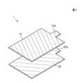
図1に示すように、本発明の透明タッチパネル1は上部電極基板10と下部電極基板20を有している。これら上部電極基板10と下部電極基板20とは板厚方向に積層された状態で貼り合わせられ、一枚の透明タッチパネル1が構成されている。 As shown in FIG. 1, the
図2に示すように、上部電極基板10は、PETやアクリルなどからなる絶縁性および可撓性を有する薄手の透明シート(第1の基板)11で形成されている。前記透明シート11の表面には、Y方向に延びる複数のX検出電極(第1の透明電極)xn(個別にx1,x2,x3,・・・,x13で示す)と複数の共通電極cn(個別にc1,c2,c3,・・・,c13で示す)がX方向に交互に配置されている。X検出電極xnと共通電極cnとは、ITO(IndiumTin Oxide;酸化インジウムスズ)など可視光の透過率の高い電極(透明電極)により形成されている。 As shown in FIG. 2, the
前記X検出電極x1,x2,x3,・・・,x13の前記共通電極cnと対向するX方向の左右両辺には、複数の凹部と凸部とからなる凹凸がY方向に沿って交互に所定の間隔で配置されている。すなわち、隣り合うX検出電極xnと共通電極cnとは所定の距離を隔てX方向の左右にて対向しており、これらの間には小さなスペース(隙間)S1,S2が形成されている。共通電極cnと前記X検出電極xnの凸部との間に形成されるスペース(第1の隙間)S1は狭く、共通電極cnと前記X検出電極xnの凹部との間に形成されるスペース(第2の隙間)S2はそれよりも広い。そして、狭いスペースS1と広いスペースS2とは、各X検出電極xnのX方向の両側位置にY方向に沿って交互に配置されている。 On the left and right sides of the X detection electrodes x1, x2, x3,..., X13 facing the common electrode cn, irregularities including a plurality of concave portions and convex portions are alternately specified along the Y direction. Are arranged at intervals. That is, the adjacent X detection electrode xn and the common electrode cn are opposed to each other in the X direction at a predetermined distance, and small spaces (gap) S1 and S2 are formed between them. A space (first gap) S1 formed between the common electrode cn and the convex portion of the X detection electrode xn is narrow, and a space formed between the common electrode cn and the concave portion of the X detection electrode xn ( The second gap S2 is wider than that. The narrow space S1 and the wide space S2 are alternately arranged along the Y direction at both side positions in the X direction of the X detection electrodes xn.
前記X検出電極xnと前記共通電極cnとの間に所定の電圧が印加されると、各電極間に静電容量が形成される。前記のように前記X検出電極x1,x2,x3,・・・,x13の左右両辺に複数の凹凸を形成しておくと、例えば共通電極c1については、前記共通電極c1とX検出電極x1との間に形成される静電容量と、前記共通電極c1とX検出電極x2との間に形成される静電容量との差(ばらつき)を小さく抑えることができる。このことは、他の共通電極cnと、これにX方向の左右両側の位置にて隣接する他のX検出電極xnとの間でも同様である。すなわち、複数の凹凸は、ある共通電極cnとこれに隣接するX検出電極xnとの間に形成される静電容量を、いずれの組み合わせにおいてもほぼ一定とすることができ、精度の高い検出を可能とする。なお、凹凸は前記X検出電極xnの左右両辺に形成されるものに限られるものではなく、前記共通電極cnの左右両辺に形成される構成であってもよいし、あるいは前記X検出電極xnと前記共通電極cnの双方に形成される構成であってもよい。 When a predetermined voltage is applied between the X detection electrode xn and the common electrode cn, a capacitance is formed between the electrodes. If a plurality of irregularities are formed on the left and right sides of the X detection electrodes x1, x2, x3,..., X13 as described above, for example, for the common electrode c1, the common electrode c1 and the X detection electrode x1 The difference (variation) between the capacitance formed between the capacitance and the capacitance formed between the common electrode c1 and the X detection electrode x2 can be reduced. This is the same between the other common electrode cn and the other X detection electrode xn adjacent to the common electrode cn at positions on the left and right sides in the X direction. That is, the plurality of irregularities can make the capacitance formed between a certain common electrode cn and the X detection electrode xn adjacent to the common electrode cn almost constant in any combination, and can detect with high accuracy. Make it possible. The irregularities are not limited to those formed on the left and right sides of the X detection electrode xn, but may be formed on both the left and right sides of the common electrode cn, or the X detection electrode xn The structure formed in both the said common electrodes cn may be sufficient.
図5に拡大して示すように、上部電極基板10側の透明シート11の前記スペースS1,S2内にはダミー電極(第3の透明電極)D1を設けられている。前記ダミー電極D1は、前記X検出電極x2または共通電極c1,c2が延びる長手方向(Y方向)を長辺とする複数の細く透明な電極線d1で形成されており、このような微細な電極線d1が並び方向(X方向)に沿って一定の間隔で配置されている。個々の電極線d1は、図5に示すように小片状に分断された状態で配置されていてもよいし、また前記X検出電極xnに形成された個々の凹部や凸部の長さ寸法と同程度の長さ寸法で形成されていてもよい。あるいはX検出電極xn自体の長さ寸法と同程度の長さ寸法を有する状態で配置されていてもよい。ただし、個々の電極線d1は、前記X検出電極xnおよび前記共通電極cnをはじめとする他のいずれの電極線d1にも接触することなく、電気的に絶縁された状態で配置されていることが好ましい。 As shown in an enlarged view in FIG. 5, dummy electrodes (third transparent electrodes) D <b> 1 are provided in the spaces S <b> 1 and S <b> 2 of the
このように電極線d1を他のいずれの電極からも絶縁させた状態にしておくと、例えばX検出電極xnと共通電極cnとの間に複数のコンデンサを直列に配置した場合と等価にできる。あるいは複数の電極線d1が有する幅寸法分だけ、X検出電極xnと共通電極cnとの対向距離が狭まった場合と等価となるため、この間の静電容量を大きくすることができる。 If the electrode line d1 is insulated from any other electrode in this way, it can be equivalent to, for example, a case where a plurality of capacitors are arranged in series between the X detection electrode xn and the common electrode cn. Alternatively, this is equivalent to the case where the opposing distance between the X detection electrode xn and the common electrode cn is reduced by the width dimension of the plurality of electrode lines d1, and thus the capacitance between them can be increased.
図1および図2に示すように、前記透明シート11のY2方向の縁部には、前記透明シート11から連続して延びる可撓性配線部10Aが形成されている。この可撓性配線部10Aには、前記X検出電極x1,x2,x3,・・・,x13から延びる引き出し線13が配線されている。各引き出し線13は、例えば銀など導電性の金属でパターン形成したものであり、互いに接することなく可撓性配線部10Aを介して外部に引き出されている。 As shown in FIGS. 1 and 2, a
またすべての共通電極c1,c2,c3,・・・,c13は、図示Y1側の位置にて図示X方向に沿うように形成された接続電極14を介して導通接続されている。前記接続電極14は、例えば銀などの導電性の金属によりパターン形成されている。そして、X方向の中央に位置する共通電極c7のY2側の端部には、同じく銀などの導電性の金属で形成した引き出し線15が接続されており、引き出し線15は可撓性配線部10Aを介して外部に引き出されている。 Further, all the common electrodes c1, c2, c3,..., C13 are conductively connected through a
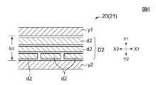
図3に示すように、下部電極基板20は、ガラス基板またはアクリルなど絶縁性を有する透明基板(第2の基板)21で形成されている。前記透明基板21の表面には、前記X検出電極Xnおよび共通電極cnと直交する図示X方向に延びる複数の複数のY検出電極(第2の透明電極))yn(個別にy1,y2,・・・,y16で示す)が配線されている。なお、Y検出電極ynもITO(IndiumTin Oxide;酸化インジウムスズ)などからなる透明電極で形成されている。 As shown in FIG. 3, the
各Y検出電極y1,y2,・・・,y16は互い平行であり、同一平面内の隣り合うY検出電極yn間にはほぼ一定の領域からなるスペース(第3の隙間)S3がそれぞれ設けられている。 Each of the Y detection electrodes y1, y2,..., Y16 is parallel to each other, and a space (third gap) S3 including a substantially constant area is provided between adjacent Y detection electrodes yn in the same plane. ing.
前記下部電極基板20に縁部には複数の引き出し線23A,23Bが設けられている。各引き出し線23Aは、Y検出電極y1ないしY検出電極y8の図示X1側の端部に個別に接続されており、下部電極基板20の図示X1側およびY2側の縁部に沿って引き回されている。同様に、各引き出し線23Bは、Y検出電極y9ないしY検出電極y16の図示X2側の端部に個別に接続されており、下部電極基板20の図示X2側およびY2側の縁部に沿って引き回されている。 The
下部電極基板20のY2側の縁部には、透明基板21の端部から連続して凸状に延びる延出部20Aが一体に形成されている。前記引き出し線23A,23Bは例えば銀など導電性の金属でパターン形成されており、互いに接することなく前記下部電極基板20のY2側の縁部および前記延出部20Aを介して外部に引き出されている。 An
図6に示すように、前記スペースS3内にはダミー電極(第3の透明電極)D2が配置されている。ダミー電極D2は、前記Y検出電極ynに対して平行となるX方向を長手方向とする細い透明な電極線d2で形成されており、このような電極線d2が前記スペースS3内に並び方向(Y方向)に一定の間隔で配置されている。前記細い電極線d2は前記Y検出電極ynと同じ長さでもよいし、または上記のようにそれよりも短い寸法からなる複数の電極線d2が長手方向に並ぶように配置されるものであってもよい。ただし、個々の電極線d2は、前記Y検出電極ynや他のいずれの電極線d2とも接触することなく、電気的に絶縁された状態で配置されている。このように電極線d2を他のいずれの電極からも絶縁させた状態にしておくと、上記同様に静電容量を大きくすることができる。 As shown in FIG. 6, a dummy electrode (third transparent electrode) D2 is disposed in the space S3. The dummy electrode D2 is formed of a thin transparent electrode line d2 whose longitudinal direction is the X direction parallel to the Y detection electrode yn. Such an electrode line d2 is aligned in the space S3 ( (Y direction) are arranged at regular intervals. The thin electrode line d2 may have the same length as the Y detection electrode yn, or a plurality of electrode lines d2 having a shorter dimension as described above are arranged in the longitudinal direction. Also good. However, the individual electrode lines d2 are arranged in an electrically insulated state without contacting the Y detection electrode yn or any other electrode line d2. When the electrode line d2 is insulated from any other electrode as described above, the capacitance can be increased as described above.
上部電極基板10は下部電極基板20の上に重ねた状態で積層される。図4に示すように、上部電極基板10側の第2のスペースS2の下に下部電極基板20側に設けられた前記Y検出電極ynが配置される。そして、上部電極基板10側の前記第1,第2のスペースS1,S2内にはダミー電極D1として電極線d1が配置され、下部電極基板20側の第3のスペースS3にはダミー電極D2として電極線d2が配線される。 The
このように、本願発明では、上部電極基板10においては第1,第2のスペースS1,S2内に多数のダミー電極D1を配置することができ、下部電極基板20においては第3のスペースS3に多数のダミー電極D2を配置することができる。このため、上部電極基板10においてはX検出電極xnや共通電極cnが形成された部分とダミー電極D1のみが形成された第1,第2のスペースS1,S2部分との間におけるコントラストの差を小さくできる。同様に、下部電極基板20においてはY検出電極ynが形成された部分とダミー電極D2のみが形成された第3のスペースS3部分との間におけるコントラストの差を小さくすることができる。よって、外部上方から透明タッチパネル1の表面を覗いたときに、内部に配線されているX検出電極xn、共通電極cnおよびY検出電極ynを見え難くすることができる。このため、このような透明タッチパネル1を携帯電話機などの液晶表示装置の上部に搭載したときであっても、前記液晶表示装置に表示された画面の視認性が低下することを避けることができる。 Thus, in the present invention, a large number of dummy electrodes D1 can be arranged in the first and second spaces S1, S2 in the
透明タッチパネル1では、前記共通電極cnを基準に、まず前記X検出電極x1ないしxnに対し所定のタイミングで電圧が順次印加され、続いて前記Y検出電極y1ないしynに対しに所定のタイミングで電圧が順次印加される。これにより、共通電極cnと各前記X検出電極x1ないしxn間、および共通電極cnと各前記X検出電極y1ないしyn間に所定の静電容量がそれぞれ所定のタイミングで順次形成される。操作者の指などが、図示しない表面パネルなどを介して透明タッチパネルの表面に接触すると、指の位置に近い部分の静電容量が変化する。このため、各静電容量の変化状態を電圧変化として検出することにより、前記指の座標位置を検出することができる。すなわち、この前記透明シート(第1の基板)11と前記透明基板(第2の基板)21とを有する透明タッチパネルは、静電容量式の座標入力手段として機能を有する。 In the
上記実施の形態では、前記共通電極cnがX検出電極x1ないしxn間に配置される構成を示したが、前記共通電極cnはY検出電極y1ないしyn間に配置される構成であってもよい。なお、前記共通電極cnは必須のものではないので、上部電極基板10が下部電極基板20と同様の構成、すなわちX検出電極x1ないしxnのみを有する構成であってもよい。 In the above embodiment, the common electrode cn is arranged between the X detection electrodes x1 to xn. However, the common electrode cn may be arranged between the Y detection electrodes y1 to yn. . Since the common electrode cn is not essential, the
次に、上記透明タッチパネルの製造方法について説明する。
図7Aないし図7Hは本発明における透明タッチパネルの製造方法を示す工程図である。Next, the manufacturing method of the said transparent touch panel is demonstrated.
7A to 7H are process diagrams showing a method for manufacturing a transparent touch panel according to the present invention.
以下においては、1枚の透明基板41上に複数の上部電極基板10または下部電極基板20を形成し、一度に複数の透明タッチパネルを製造する方法について説明する。なお、以下の第1工程から第8の工程までは上部電極基板10と下部電極基板20との間で共通である。 Hereinafter, a method of forming a plurality of transparent touch panels at a time by forming a plurality of
図7Aに示すように、第1の工程では、透明基板41の上に透明抵抗層42を形成する。前記透明基板41は、上記の透明シート11および透明基板21に相当する。透明抵抗層42は、ITO(Indium TinOxide;酸化インジウムスズ)であり、例えばスパッタ法や真空蒸着法などを用いて成膜され、後述するように透明電極を形成する。 As shown in FIG. 7A, in the first step, the
図7Bに示すように、第2の工程では、透明抵抗層42の表面にレジスト層43が印刷等の手段により形成される。このとき使用されるレジスト層43は、例えば緑色のような有色のレジスト材が使用される。 As shown in FIG. 7B, in the second step, a resist
図7Cに示すように、第3の工程では、前記レジスト層43に配線パターンが形成されたマスク50を対向配置した状態で露光することにより、前記所定の配線パターンが前記レジスト層43に焼き付けられる。なお、上部電極基板10用のマスク50にはX検出電極xn、共通電極cnおよびダミー電極D1を形成するための孔が形成されており、下部電極基板20用のマスク50にはY検出電極ynおよびダミー電極D2を形成するための孔が形成されている。 As shown in FIG. 7C, in the third step, the predetermined wiring pattern is baked on the resist
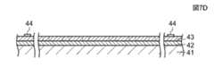
図7Dに示すように、第4の工程では、前記レジスト層43上の所定の位置に位置決め用の第2のレジストからなるマーク44が部分的に印刷される。前記マーク44を形成する第2のレジストは、前記レジスト層43と見分けが付く程度に異なる色であることが好ましい。あるいは、マーク44の下層側に位置するレジスト層43の色が透けて見えるように、第2のレジストを透明な色のレジスト材で形成した構成であってもよい。 As shown in FIG. 7D, in the fourth step, a
前記マーク44が印刷される位置は、例えば前記X検出電極xn、共通電極cnおよびダミー電極D1が形成される領域の外側の縁(欄外の位置)が好ましい。前記マーク44を形成する第2のレジストは、透明タッチパネル1の組立て時における位置決め用のマーク44であり、組立て完成後は不要となる。このため、前記のようにマーク44を前記欄外の位置に形成しておくと、透明タッチパネル1の組立て完成後に容易に切除することが可能となる。 The position where the
なお、前記第2のレジストを、前記レジスト層43上の少なくとも2箇所以上の位置に形成する構成とすれば、第8の工程以下に説明する位置決めのためのマーク44として用いることが可能である。 If the second resist is formed at at least two positions on the resist
前記第3の工程と第4の工程の順番は逆の関係であってもよい。すなわち。前記レジスト層43上の所定の位置に位置決め用の第2のレジスト(マーク44)が部分的に印刷され、その後にマスクを用いての露光を行うものであってもよい。この場合、マスク50の位置決めが、前記マーク44を基準に高精度に行うことが可能となる。 The order of the third step and the fourth step may be reversed. That is. The positioning second resist (mark 44) may be partially printed at a predetermined position on the resist
図7Eに示すように、第5の工程では前記レジスト層43の現像を行う。このとき、透明基板41の上には必要なレジスト層43だけが残り、不要なレジスト層43が除去される。また第2のレジストからなるマーク44は除去されず、その下に位置するレジスト層43とともに残される。 As shown in FIG. 7E, in the fifth step, the resist
図7Fに示すように、第6の工程では、透明抵抗層42に対しエッチング処理を行うことにより、前記透明基板41の上に所定の形状からなる透明電極が形成される。すなわち、上部電極基板10であればX検出電極xn、共通電極cnおよびダミー電極D1が形成され、下部電極基板20であればY検出電極ynおよびダミー電極D2が形成される。なお、このときには、前記透明基板41上に第2のレジスト(マーク44)が残されている。 As shown in FIG. 7F, in the sixth step, a transparent electrode having a predetermined shape is formed on the
図7Gに示すように、第7の工程では、マーク44を形成する第2のレジストの部分を除くすべてのレジスト層43が前記透明基板41上から除去される。 As shown in FIG. 7G, in the seventh step, all of the resist
上部電極基板10および下部電極基板20は、上記第1の工程ないし第7の工程が行われることによりそれぞれ形成される。 The
第8の工程では、上記第1の工程ないし第7の工程を経て形成された上部電極基板10と下部電極基板20の表面が、カメラを有する画像認識装置(図示せず)を用いて撮影され、その画像データがそれぞれ別々に読み込まれる。前記画像認識装置では、上部電極基板10および下部電極基板20の表面の2箇所以上の箇所に設けられているマーク44の位置をパターン認識し、前記マーク44を基準とする座標データを作成する。そして、前記マーク44を基準とした上で、前記透明基板41の表面に各種の導線が銀などの導電性材料を用いて印刷される。すなわち、上部電極基板10の場合には、透明シート11の縁部に前記マーク44を基準として引き出し線13,15および接続電極14が印刷される。同様に、上部電極基板10の場合には、透明基板21の縁部に前記マーク44を基準として引き出し線23A,23Bが印刷される。このため、上部電極基板10に形成された引き出し線13,15および接続電極14、下部電極基板20に形成された引き出し線23A,23Bなどを高精度に配線することができる。よって、下部電極基板20の上に上部電極基板10を積層したときに、上部電極基板10側のX検出電極xnと下部電極基板20側のY検出電極ynとの間での、水平面に平行な方向における位置ずれ量を小さくするとができるため、精度の高い透明タッチパネルを形成することができる。 In the eighth step, the surfaces of the
図7Hに示すように、第9の工程では、前記マーク44を基準として、下部電極基板20と、その上に積層された上部電極基板10とが張り合わされる。これにより、複数の透明タッチパネル1を有するシート状の透明タッチパネルが一体的に製造される。この一体化されたシート状の透明タッチパネル1では、各下部電極基板20の上に各上部電極基板10が高精度に位置決めされている。 As shown in FIG. 7H, in the ninth step, the
続く第10の工程では、前記シート状の透明タッチパネルが、個々の透明タッチパネルに切り分けられ分離される。この際、前記欄外の位置に設けられたマーク44を形成する第2のレジストおよびその下部のレジスト層43が、前記透明タッチパネルから同時に切除される。これにより、透明タッチパネル1が完成する。 In the subsequent tenth step, the sheet-like transparent touch panel is cut and separated into individual transparent touch panels. At this time, the second resist forming the
上記実施の形態では、第9ないし第10の工程において、シート状の透明タッチパネルを一体的に形成した後に、切り分けて個々の透明タッチパネルを完成させる工程をしたが本発明はこれに限られるものはない。すなわち、第8の工程の次に、前記透明基板21に形成された下部電極基板20とを個々の下部電極基板20に切り分け、さらに前記透明シート11に形成された上部電極基板10とを個々の上部電極基板10に切り分け、その後に前記分離後の下部電極基板20の上に前記分離後の上部電極基板10を重ねることにより、透明タッチパネルを完成させる構成であってもよい。 In the above embodiment, after the sheet-like transparent touch panel is integrally formed in the ninth to tenth steps, the process of cutting and completing each transparent touch panel is performed, but the present invention is not limited to this. Absent. That is, after the eighth step, the
1 透明タッチパネル
10 上部電極基板
11 透明シート
13,15 引き出し線
14 接続電極
20 下部電極基板
21 透明基板
23A,23B 引き出し線
x1〜xn X検出電極(第1の透明電極)
y1〜yn X検出電極(第2の透明電極)
D1,D2 ダミー電極(第3の透明電極)
d1,d2 電極線
S1 第1のスペース(第1の隙間)
S2 第2のスペース(第2の隙間)
S3 第3のスペース(第3の隙間)DESCRIPTION OF
y1 to yn X detection electrodes (second transparent electrodes)
D1, D2 dummy electrode (third transparent electrode)
d1, d2 electrode line S1 first space (first gap)
S2 Second space (second gap)
S3 Third space (third gap)
Claims (10)
Translated fromJapanese(a)透明基板上に透明抵抗層を形成する工程と、
(b)前記透明抵抗層の表面にレジスト層を形成し、且つ前記レジスト層に所定のマスクを当てて露光することにより所定の配線パターンを焼き付ける工程と、
(c)前記レジスト層に位置決め用のマークを形成する工程と、
(d)前記レジスト層の前記マークを除く部分を現像し、且つエッチング処理を行うことにより、透明基板上に前記第1の透明電極または前記第2の透明電極を形成する工程と、
(e)前記透明基板上の画像を位置決めマークとともに取り込むとともに、取り込んだ前記位置決めマークを基準として前記透明基板上に所定の引き出し線を印刷する工程と、
(f)前記第2の透明電極が配置された第2の基板の上に、前記第1の透明電極が配置された第1の基板を重ねた状態で両基板を貼り合わせる工程と、
(g)前記貼り合わされた両基板を個々の透明タッチパネルに切断し、このとき前記マークを一緒に切除する工程と、
を有することを特徴とする透明タッチパネルの製造方法。A method for manufacturing a transparent touch panel according to any one of claims 1 to 8,
(A) forming a transparent resistance layer on the transparent substrate;
(B) forming a resist layer on the surface of the transparent resistance layer and baking a predetermined wiring pattern by exposing the resist layer to a predetermined mask; and
(C) forming a positioning mark on the resist layer;
(D) forming the first transparent electrode or the second transparent electrode on a transparent substrate by developing a portion of the resist layer excluding the mark and performing an etching process;
(E) capturing an image on the transparent substrate together with a positioning mark, and printing a predetermined lead line on the transparent substrate based on the captured positioning mark;
(F) bonding the two substrates together in a state where the first substrate on which the first transparent electrode is disposed is overlaid on the second substrate on which the second transparent electrode is disposed;
(G) cutting the bonded substrates into individual transparent touch panels, and cutting the marks together at this time;
A method for producing a transparent touch panel, comprising:
Priority Applications (1)
| Application Number | Priority Date | Filing Date | Title |
|---|---|---|---|
| JP2006311794AJP2008129708A (en) | 2006-11-17 | 2006-11-17 | Transparent touch panel and its manufacturing method |
Applications Claiming Priority (1)
| Application Number | Priority Date | Filing Date | Title |
|---|---|---|---|
| JP2006311794AJP2008129708A (en) | 2006-11-17 | 2006-11-17 | Transparent touch panel and its manufacturing method |
Publications (1)
| Publication Number | Publication Date |
|---|---|
| JP2008129708Atrue JP2008129708A (en) | 2008-06-05 |
Family
ID=39555479
Family Applications (1)
| Application Number | Title | Priority Date | Filing Date |
|---|---|---|---|
| JP2006311794AWithdrawnJP2008129708A (en) | 2006-11-17 | 2006-11-17 | Transparent touch panel and its manufacturing method |
Country Status (1)
| Country | Link |
|---|---|
| JP (1) | JP2008129708A (en) |
Cited By (48)
| Publication number | Priority date | Publication date | Assignee | Title |
|---|---|---|---|---|
| JP2010002958A (en)* | 2008-06-18 | 2010-01-07 | Epson Imaging Devices Corp | Capacitance input device, and display device with input function |
| JP2010009439A (en)* | 2008-06-30 | 2010-01-14 | Hitachi Displays Ltd | Display apparatus with touch panel |
| JP2010039816A (en)* | 2008-08-06 | 2010-02-18 | Hitachi Displays Ltd | Display |
| JP2010108222A (en)* | 2008-10-30 | 2010-05-13 | Kyocera Corp | Touch panel and touch panel type display device |
| JP2010197576A (en)* | 2009-02-24 | 2010-09-09 | Sony Corp | Display device and method of manufacturing same |
| JP2010218535A (en)* | 2009-02-20 | 2010-09-30 | Alps Electric Co Ltd | Capacitance type input device |
| JP2010250424A (en)* | 2009-04-13 | 2010-11-04 | Polymatech Co Ltd | Touch pad and touch panel |
| JP2010282501A (en)* | 2009-06-05 | 2010-12-16 | Sony Corp | Touch panel, display panel and display |
| CN101930301A (en)* | 2009-06-18 | 2010-12-29 | 株式会社和冠 | Indication body pick-up unit and indication body detection method |
| JP2011008706A (en)* | 2009-06-29 | 2011-01-13 | Sony Corp | Information input device and display device |
| JP2011065515A (en)* | 2009-09-18 | 2011-03-31 | Hitachi Displays Ltd | Display device |
| JP2011076610A (en)* | 2009-09-29 | 2011-04-14 | Lg Innotek Co Ltd | Multi-resistance film touch screen and manufacturing method of the same |
| JP2011100357A (en)* | 2009-11-06 | 2011-05-19 | Hosiden Corp | Touch panel and manufacturing method therefor |
| KR101048980B1 (en)* | 2009-01-16 | 2011-07-12 | 삼성모바일디스플레이주식회사 | Touch screen panel and its manufacturing method |
| JP2011146023A (en)* | 2009-09-17 | 2011-07-28 | Panasonic Corp | Touch panel |
| WO2011093420A1 (en) | 2010-01-28 | 2011-08-04 | 富士フイルム株式会社 | Conductive sheet, method for using conductive sheet, and touch panel |
| JP2012014669A (en)* | 2009-11-20 | 2012-01-19 | Fujifilm Corp | Conductive sheet, method of using conductive sheet and electrostatic capacitive touch panel |
| KR101144568B1 (en)* | 2008-10-31 | 2012-05-11 | 엘지이노텍 주식회사 | Input device |
| JP2012178193A (en)* | 2012-06-22 | 2012-09-13 | Japan Display East Co Ltd | Display device |
| JP2012532336A (en)* | 2009-06-30 | 2012-12-13 | スリーエム イノベイティブ プロパティズ カンパニー | Electronic display with figure and metal micropatterned substrate |
| US20130127784A1 (en)* | 2011-11-22 | 2013-05-23 | Qualcomm Mems Technologies, Inc. | Methods and apparatuses for hiding optical contrast features |
| US8456444B2 (en) | 2009-03-04 | 2013-06-04 | Japan Display West, Inc. | Display apparatus |
| US8462129B2 (en) | 2009-05-29 | 2013-06-11 | Mitsubishi Electric Corporation | Touch panel and display apparatus having the same |
| WO2013111795A1 (en)* | 2012-01-24 | 2013-08-01 | デクセリアルズ株式会社 | Transparent conductive element, input device, electronic apparatus and master for production of transparent conductive element |
| JP2013218659A (en)* | 2012-04-09 | 2013-10-24 | Samsung Display Co Ltd | Display device |
| CN103384870A (en)* | 2011-02-18 | 2013-11-06 | 富士胶片株式会社 | Electroconductive sheet and touch panel |
| CN103513848A (en)* | 2012-06-21 | 2014-01-15 | 赛普拉斯半导体公司 | Sensor pattern with inactive electrodes for mutual capacitance in the emitting TX layer |
| JP2014017010A (en)* | 2013-09-19 | 2014-01-30 | Japan Display Inc | Display device |
| JP5442012B2 (en)* | 2009-06-30 | 2014-03-12 | 京セラ株式会社 | Coordinate input device and display device with coordinate input function |
| WO2014046160A1 (en)* | 2012-09-24 | 2014-03-27 | 日本写真印刷株式会社 | Touch panel, and touch panel production method |
| US8722314B2 (en) | 2010-05-28 | 2014-05-13 | Fujifilm Corporation | Method for producing conductive sheet and method for producing touch panel |
| US8889244B2 (en) | 2011-06-29 | 2014-11-18 | Dexerials Corporation | Transparent electrode device, information input device, and electronic equipment |
| JP2015014964A (en)* | 2013-07-05 | 2015-01-22 | 大日本印刷株式会社 | Touch panel sensor and display device with touch position detection function |
| WO2015008934A1 (en)* | 2013-07-16 | 2015-01-22 | Lg Innotek Co., Ltd. | Touch window |
| WO2015025487A1 (en)* | 2013-08-23 | 2015-02-26 | パナソニックIpマネジメント株式会社 | Touch panel |
| JP2015056470A (en)* | 2013-09-11 | 2015-03-23 | 株式会社ジャパンディスプレイ | Organic electroluminescence device with input function |
| US9081447B2 (en) | 2010-08-23 | 2015-07-14 | Japan Display Inc. | Display device with touch detection function, touch detection device, and electronic unit |
| US9122359B2 (en) | 2010-08-19 | 2015-09-01 | Japan Display Inc. | Display unit with touch detection function, and electronic device |
| US9182851B2 (en) | 2009-12-29 | 2015-11-10 | Qualcomm Mems Technologies, Inc. | Illumination device with metalized light-turning features |
| JP2016524739A (en)* | 2013-05-01 | 2016-08-18 | アップル インコーポレイテッド | Display with integrated touch and improved image pixel aperture |
| CN105912153A (en)* | 2010-09-14 | 2016-08-31 | 株式会社日本显示器 | Display Device With Touch Detection Function, And Electronic Unit |
| US9454279B2 (en) | 2009-04-20 | 2016-09-27 | Japan Display Inc. | Display device with capacitive touch sensor with slit formed in a surface of a detectng electrode opposed to a scanning electrode to realize detection with high accuracy |
| US10061420B2 (en) | 2014-09-26 | 2018-08-28 | Japan Display Inc. | Sensor-equipped display device and method of controlling the same |
| JP2018152122A (en)* | 2013-02-27 | 2018-09-27 | ミラエナノテック カンパニー リミテッド | Structure of touch pad using dummy pattern for capacitance type touch screen |
| KR20190038803A (en) | 2016-07-26 | 2019-04-09 | 파나소닉 아이피 매니지먼트 가부시키가이샤 | LIQUID CRYSTAL FOR ELECTROPHOTABLE ELECTRODE, TRANSFORMING ELECTRODE MATERIAL, DEVICE AND METHOD FOR MANUFACTURING LAMINATED PANEL |
| KR20190044625A (en) | 2016-09-07 | 2019-04-30 | 파나소닉 아이피 매니지먼트 가부시키가이샤 | Member for a touch panel |
| KR20190105562A (en) | 2017-01-23 | 2019-09-17 | 닛샤 가부시키가이샤 | Capacitive touch panel |
| KR20230156064A (en) | 2021-03-16 | 2023-11-13 | 닛샤 가부시키가이샤 | Capacitive touch panel |
- 2006
- 2006-11-17JPJP2006311794Apatent/JP2008129708A/ennot_activeWithdrawn
Cited By (100)
| Publication number | Priority date | Publication date | Assignee | Title |
|---|---|---|---|---|
| JP2010002958A (en)* | 2008-06-18 | 2010-01-07 | Epson Imaging Devices Corp | Capacitance input device, and display device with input function |
| US8400418B2 (en) | 2008-06-18 | 2013-03-19 | Sony Corporation | Capacitance type input device and display device with input function |
| KR101086559B1 (en)* | 2008-06-18 | 2011-11-23 | 소니 주식회사 | Capacitive input device and display device with input function |
| JP2010009439A (en)* | 2008-06-30 | 2010-01-14 | Hitachi Displays Ltd | Display apparatus with touch panel |
| JP2010039816A (en)* | 2008-08-06 | 2010-02-18 | Hitachi Displays Ltd | Display |
| JP2010108222A (en)* | 2008-10-30 | 2010-05-13 | Kyocera Corp | Touch panel and touch panel type display device |
| KR101144568B1 (en)* | 2008-10-31 | 2012-05-11 | 엘지이노텍 주식회사 | Input device |
| KR101048980B1 (en)* | 2009-01-16 | 2011-07-12 | 삼성모바일디스플레이주식회사 | Touch screen panel and its manufacturing method |
| US8847893B2 (en) | 2009-01-16 | 2014-09-30 | Samsung Display Co., Ltd. | Touch screen panel and method of fabricating the same |
| JP2010218535A (en)* | 2009-02-20 | 2010-09-30 | Alps Electric Co Ltd | Capacitance type input device |
| US9013642B2 (en) | 2009-02-24 | 2015-04-21 | Japan Display Inc. | Display device |
| US11960673B2 (en) | 2009-02-24 | 2024-04-16 | Japan Display Inc. | Display device and method of manufacturing same |
| US11068097B2 (en) | 2009-02-24 | 2021-07-20 | Japan Display Inc. | Display device and method of manufacturing same |
| US11599214B2 (en) | 2009-02-24 | 2023-03-07 | Japan Display Inc. | Display device and method of manufacturing same |
| US9459718B2 (en) | 2009-02-24 | 2016-10-04 | Japan Display Inc. | Display device and method of manufacturing same |
| US9791951B2 (en) | 2009-02-24 | 2017-10-17 | Japan Display Inc. | Display device and method of manufacturing same |
| JP2010197576A (en)* | 2009-02-24 | 2010-09-09 | Sony Corp | Display device and method of manufacturing same |
| US10649563B2 (en) | 2009-02-24 | 2020-05-12 | Japan Display Inc. | Display device and method of manufacturing same |
| US12287931B2 (en) | 2009-02-24 | 2025-04-29 | Japan Display Inc. | Display device and method of manufacturing same |
| US8456444B2 (en) | 2009-03-04 | 2013-06-04 | Japan Display West, Inc. | Display apparatus |
| JP2010250424A (en)* | 2009-04-13 | 2010-11-04 | Polymatech Co Ltd | Touch pad and touch panel |
| US10275085B2 (en) | 2009-04-20 | 2019-04-30 | Japan Display Inc. | Display device with capacitive touch sensor with slit formed in a surface of a detecting electrode opposed to a scanning electrode to realize detection with high accuracy |
| US9652075B2 (en) | 2009-04-20 | 2017-05-16 | Japan Display Inc. | Display device with capacitive touch sensor with slit formed in a surface of a detecting electrode opposed to a scanning electrode to realize detection with high accuracy |
| US10025425B2 (en) | 2009-04-20 | 2018-07-17 | Japan Display Inc. | Display device with capacitive touch sensor with slit formed in a surface of a detecting electrode opposed to a scanning electrode to realize detection with high accuracy |
| US9454279B2 (en) | 2009-04-20 | 2016-09-27 | Japan Display Inc. | Display device with capacitive touch sensor with slit formed in a surface of a detectng electrode opposed to a scanning electrode to realize detection with high accuracy |
| US10817108B2 (en) | 2009-04-20 | 2020-10-27 | Japan Display Inc. | Display device with capacitive touch sensor with slit formed in a surface of a detecting electrode opposed to a scanning electrode to realize detection with high accuracy |
| US8462129B2 (en) | 2009-05-29 | 2013-06-11 | Mitsubishi Electric Corporation | Touch panel and display apparatus having the same |
| JP2010282501A (en)* | 2009-06-05 | 2010-12-16 | Sony Corp | Touch panel, display panel and display |
| CN101930301A (en)* | 2009-06-18 | 2010-12-29 | 株式会社和冠 | Indication body pick-up unit and indication body detection method |
| JP2011008706A (en)* | 2009-06-29 | 2011-01-13 | Sony Corp | Information input device and display device |
| US9013415B2 (en) | 2009-06-29 | 2015-04-21 | Japan Display Inc. | Information input device including a detection electrode with an aperture |
| JP2012532336A (en)* | 2009-06-30 | 2012-12-13 | スリーエム イノベイティブ プロパティズ カンパニー | Electronic display with figure and metal micropatterned substrate |
| US9060434B2 (en) | 2009-06-30 | 2015-06-16 | 3M Innovative Properties Company | Electronic displays and metal micropatterned substrates having a graphic |
| JP5442012B2 (en)* | 2009-06-30 | 2014-03-12 | 京セラ株式会社 | Coordinate input device and display device with coordinate input function |
| JP2011146023A (en)* | 2009-09-17 | 2011-07-28 | Panasonic Corp | Touch panel |
| JP2011065515A (en)* | 2009-09-18 | 2011-03-31 | Hitachi Displays Ltd | Display device |
| CN102033676A (en)* | 2009-09-29 | 2011-04-27 | Lg伊诺特有限公司 | Resistance type touch screen capable of detecting multi-point touch and manufacturing method of the same |
| TWI419038B (en)* | 2009-09-29 | 2013-12-11 | Lg Innotek Co Ltd | Resistive type touch screen capable of detecting multi-touch and manufacturing method of the same |
| JP2011076610A (en)* | 2009-09-29 | 2011-04-14 | Lg Innotek Co Ltd | Multi-resistance film touch screen and manufacturing method of the same |
| JP2011100357A (en)* | 2009-11-06 | 2011-05-19 | Hosiden Corp | Touch panel and manufacturing method therefor |
| JP2012014669A (en)* | 2009-11-20 | 2012-01-19 | Fujifilm Corp | Conductive sheet, method of using conductive sheet and electrostatic capacitive touch panel |
| US9182851B2 (en) | 2009-12-29 | 2015-11-10 | Qualcomm Mems Technologies, Inc. | Illumination device with metalized light-turning features |
| US9817534B2 (en) | 2009-12-29 | 2017-11-14 | Snaptrack, Inc. | Illumination device with metalized light-turning features |
| US10268330B2 (en) | 2010-01-28 | 2019-04-23 | Fujifilm Corporation | Conductive component and conductive component for touch panel |
| US10430014B2 (en) | 2010-01-28 | 2019-10-01 | Fujifilm Corporation | Conductive component and conductive component for touch panel |
| US9684423B2 (en) | 2010-01-28 | 2017-06-20 | Fujifilm Corporation | Conductive sheet and conductive sheet for touch panel |
| US9851860B2 (en) | 2010-01-28 | 2017-12-26 | Fujifilm Corporation | Conductive sheet and conductive sheet for touch panel |
| WO2011093420A1 (en) | 2010-01-28 | 2011-08-04 | 富士フイルム株式会社 | Conductive sheet, method for using conductive sheet, and touch panel |
| US10055080B2 (en) | 2010-01-28 | 2018-08-21 | Fujifilm Corporation | Conductive member, touch sensor and touch panel |
| US8917252B2 (en) | 2010-01-28 | 2014-12-23 | Fujifilm Corporation | Conductive sheet, method for using conductive sheet, and touch panel |
| US10031635B2 (en) | 2010-01-28 | 2018-07-24 | Fujifilm Corporation | Conductive member, touch sensor and touch panel |
| US8722314B2 (en) | 2010-05-28 | 2014-05-13 | Fujifilm Corporation | Method for producing conductive sheet and method for producing touch panel |
| US9122359B2 (en) | 2010-08-19 | 2015-09-01 | Japan Display Inc. | Display unit with touch detection function, and electronic device |
| US9619098B2 (en) | 2010-08-19 | 2017-04-11 | Japan Display Inc. | Display unit with touch detection function, and electronic device |
| US10162470B2 (en) | 2010-08-19 | 2018-12-25 | Japan Display Inc. | Display unit with touch detection function, and electronic device |
| US10386984B2 (en) | 2010-08-19 | 2019-08-20 | Japan Display Inc. | Display unit with touch detection function, and electronic device |
| US10061418B2 (en) | 2010-08-23 | 2018-08-28 | Japan Display Inc. | Display device with touch detection function, touch detection device, and electronic unit |
| US10365745B2 (en) | 2010-08-23 | 2019-07-30 | Japan Display Inc. | Display device with touch detection function, touch detection device, and electronic unit |
| US9081447B2 (en) | 2010-08-23 | 2015-07-14 | Japan Display Inc. | Display device with touch detection function, touch detection device, and electronic unit |
| US9606661B2 (en) | 2010-08-23 | 2017-03-28 | Japan Display Inc. | Display device with touch detection function, touch detection device, and electronic unit |
| US11531416B2 (en) | 2010-09-14 | 2022-12-20 | Japan Display Inc. | Display device with touch detection function, and electronic unit |
| US11119594B2 (en) | 2010-09-14 | 2021-09-14 | Japan Display Inc. | Display device with touch detection function, and electronic unit |
| CN105912153A (en)* | 2010-09-14 | 2016-08-31 | 株式会社日本显示器 | Display Device With Touch Detection Function, And Electronic Unit |
| US10156948B2 (en) | 2010-09-14 | 2018-12-18 | Japan Display Inc. | Display device with touch detection function, and electronic unit |
| US10386981B2 (en) | 2010-09-14 | 2019-08-20 | Japan Display Inc. | Display device with touch detection function, and electronic unit |
| CN105912153B (en)* | 2010-09-14 | 2019-03-01 | 株式会社日本显示器 | Display device with touch detection function |
| US9442608B2 (en) | 2010-09-14 | 2016-09-13 | Japan Display Inc. | Display device with touch detection function, and electronic unit |
| KR101838755B1 (en)* | 2010-09-14 | 2018-03-14 | 가부시키가이샤 재팬 디스프레이 | Display device with touch detection funcion, and electronic unit |
| CN103384870A (en)* | 2011-02-18 | 2013-11-06 | 富士胶片株式会社 | Electroconductive sheet and touch panel |
| US8889244B2 (en) | 2011-06-29 | 2014-11-18 | Dexerials Corporation | Transparent electrode device, information input device, and electronic equipment |
| US20130127784A1 (en)* | 2011-11-22 | 2013-05-23 | Qualcomm Mems Technologies, Inc. | Methods and apparatuses for hiding optical contrast features |
| WO2013111795A1 (en)* | 2012-01-24 | 2013-08-01 | デクセリアルズ株式会社 | Transparent conductive element, input device, electronic apparatus and master for production of transparent conductive element |
| JP2013152579A (en)* | 2012-01-24 | 2013-08-08 | Dexerials Corp | Transparent conductive element, input device, electronic apparatus, and master for manufacturing transparent conductive element |
| JP2013218659A (en)* | 2012-04-09 | 2013-10-24 | Samsung Display Co Ltd | Display device |
| CN103513848A (en)* | 2012-06-21 | 2014-01-15 | 赛普拉斯半导体公司 | Sensor pattern with inactive electrodes for mutual capacitance in the emitting TX layer |
| JP2012178193A (en)* | 2012-06-22 | 2012-09-13 | Japan Display East Co Ltd | Display device |
| WO2014046160A1 (en)* | 2012-09-24 | 2014-03-27 | 日本写真印刷株式会社 | Touch panel, and touch panel production method |
| CN104620205A (en)* | 2012-09-24 | 2015-05-13 | 日本写真印刷株式会社 | Touch panel, and touch panel production method |
| JP2014063413A (en)* | 2012-09-24 | 2014-04-10 | Nissha Printing Co Ltd | Touch panel, and manufacturing method of touch panel |
| US9292041B2 (en) | 2012-09-24 | 2016-03-22 | Nissha Printing Co., Ltd. | Touch panel and method of manufacturing touch panel |
| CN104620205B (en)* | 2012-09-24 | 2016-09-28 | 日本写真印刷株式会社 | Touch panel and the manufacture method of touch panel |
| KR101562175B1 (en) | 2012-09-24 | 2015-10-20 | 니혼샤신 인사츠 가부시키가이샤 | Touch panel, and touch panel production method |
| JP2018152122A (en)* | 2013-02-27 | 2018-09-27 | ミラエナノテック カンパニー リミテッド | Structure of touch pad using dummy pattern for capacitance type touch screen |
| JP2016524739A (en)* | 2013-05-01 | 2016-08-18 | アップル インコーポレイテッド | Display with integrated touch and improved image pixel aperture |
| JP2015014964A (en)* | 2013-07-05 | 2015-01-22 | 大日本印刷株式会社 | Touch panel sensor and display device with touch position detection function |
| US9830013B2 (en) | 2013-07-16 | 2017-11-28 | Lg Innotek Co., Ltd. | Touch window |
| WO2015008934A1 (en)* | 2013-07-16 | 2015-01-22 | Lg Innotek Co., Ltd. | Touch window |
| WO2015025487A1 (en)* | 2013-08-23 | 2015-02-26 | パナソニックIpマネジメント株式会社 | Touch panel |
| JP2015056470A (en)* | 2013-09-11 | 2015-03-23 | 株式会社ジャパンディスプレイ | Organic electroluminescence device with input function |
| US9666648B2 (en) | 2013-09-11 | 2017-05-30 | Japan Display Inc. | Organic electroluminescent display device having an input function |
| JP2014017010A (en)* | 2013-09-19 | 2014-01-30 | Japan Display Inc | Display device |
| CN105467699B (en)* | 2014-09-26 | 2018-09-28 | 株式会社日本显示器 | The control method of display device and display device with sensor |
| US10061420B2 (en) | 2014-09-26 | 2018-08-28 | Japan Display Inc. | Sensor-equipped display device and method of controlling the same |
| US10691276B2 (en) | 2016-07-26 | 2020-06-23 | Panasonic Intellectual Property Management Co., Ltd. | Laminate for see-through electrodes, see-through electrode material, device and method for producing laminate for see-through electrodes |
| KR20190038803A (en) | 2016-07-26 | 2019-04-09 | 파나소닉 아이피 매니지먼트 가부시키가이샤 | LIQUID CRYSTAL FOR ELECTROPHOTABLE ELECTRODE, TRANSFORMING ELECTRODE MATERIAL, DEVICE AND METHOD FOR MANUFACTURING LAMINATED PANEL |
| US10739923B2 (en) | 2016-09-07 | 2020-08-11 | Panasonic Intellectual Property Management Co., Ltd. | Touch panel member |
| KR20190044625A (en) | 2016-09-07 | 2019-04-30 | 파나소닉 아이피 매니지먼트 가부시키가이샤 | Member for a touch panel |
| US10496232B2 (en) | 2017-01-23 | 2019-12-03 | Nissha Co., Ltd. | Capacitive touch panel |
| KR20190105562A (en) | 2017-01-23 | 2019-09-17 | 닛샤 가부시키가이샤 | Capacitive touch panel |
| KR20230156064A (en) | 2021-03-16 | 2023-11-13 | 닛샤 가부시키가이샤 | Capacitive touch panel |
Similar Documents
| Publication | Publication Date | Title |
|---|---|---|
| JP2008129708A (en) | Transparent touch panel and its manufacturing method | |
| US9811221B2 (en) | Input device, method of manufacturing the same, and electronic information equipment | |
| US9798430B2 (en) | Input device, method of manufacturing the same, and electronic information equipment | |
| JP6702890B2 (en) | Array substrate, manufacturing method and driving method thereof, and display device | |
| EP2737390B1 (en) | Capacitive touch panel and a method of manufacturing the same | |
| JP5483143B2 (en) | Color filter, display device, and method of manufacturing color filter | |
| WO2010016174A1 (en) | Touch panel, display, and electronic device | |
| EP3040825A1 (en) | Ultra high resolution flat panel display having in-cell type touch sensor | |
| KR102189012B1 (en) | Electrode for touch sensor, touch panel, and display device | |
| JP4811502B2 (en) | Liquid crystal display panel and touch panel | |
| US20110175846A1 (en) | Touch display panel | |
| JP5780455B2 (en) | Projection-type capacitive touch panel sensor and method for manufacturing the same, and display device including projection-type capacitive touch panel sensor | |
| CN107037909B (en) | Touch detection device and display device with touch detection function | |
| CN101553776A (en) | Touch panel apparatus and method for manufacturing the same | |
| JP2020537199A (en) | Touch panel and its manufacturing method, touch display panel | |
| KR20140004100A (en) | 3d touch control liquid crystal lens grating, method for manufacturing the same and 3d touch control display device | |
| JP2012103761A (en) | Touch panel | |
| CN102236187B (en) | touch display panel | |
| JP6233075B2 (en) | Touch panel sensor and input / output device including touch panel sensor | |
| JP2011100326A (en) | Motherboard for touch panel and method for manufacturing the same | |
| JP5375692B2 (en) | Manufacturing method of touch panel sensor | |
| JP4900421B2 (en) | Liquid crystal display panel and liquid crystal display device | |
| CN106339120A (en) | Touch detection device and display device with touch detection function | |
| JP2012068287A (en) | Color filter substrate and method of manufacturing the same | |
| JP2012220670A (en) | Color filter with touch panel electrode and manufacturing method therefor |
Legal Events
| Date | Code | Title | Description |
|---|---|---|---|
| A621 | Written request for application examination | Free format text:JAPANESE INTERMEDIATE CODE: A621 Effective date:20080828 | |
| A761 | Written withdrawal of application | Free format text:JAPANESE INTERMEDIATE CODE: A761 Effective date:20090708 |