JP2008117371A - Approach detection type information display device and information display method using the same - Google Patents
Approach detection type information display device and information display method using the sameDownload PDFInfo
- Publication number
- JP2008117371A JP2008117371AJP2007233361AJP2007233361AJP2008117371AJP 2008117371 AJP2008117371 AJP 2008117371AJP 2007233361 AJP2007233361 AJP 2007233361AJP 2007233361 AJP2007233361 AJP 2007233361AJP 2008117371 AJP2008117371 AJP 2008117371A
- Authority
- JP
- Japan
- Prior art keywords
- detection
- electrode
- display
- information display
- display device
- Prior art date
- Legal status (The legal status is an assumption and is not a legal conclusion. Google has not performed a legal analysis and makes no representation as to the accuracy of the status listed.)
- Granted
Links
Images


Landscapes
- Position Input By Displaying (AREA)
- Liquid Crystal Display Device Control (AREA)
- Control Of Indicators Other Than Cathode Ray Tubes (AREA)
- Controls And Circuits For Display Device (AREA)
Abstract
Description
Translated fromJapaneseこの発明は近接検知型情報表示装置およびこれを使用した情報表示方法に関する。詳しくは、パネル状をなすパネルセンサ面への接触状態はもちろんのこと、対峙したパネルセンサ面の空間位置(非接触状態)を検知できるようにしたものである。また、非接触状態の指などの動きに応じて表示パネルに表示された映像などの表示状態に変化を持たせるなどして、今までにない情報表示状態(表示態様)を具現したものである。 The present invention relates to a proximity detection type information display device and an information display method using the same. Specifically, not only the state of contact with the panel sensor surface in the form of a panel but also the spatial position (non-contact state) of the facing panel sensor surface can be detected. In addition, an information display state (display mode) that has never existed is realized by changing the display state of an image or the like displayed on the display panel according to the movement of a finger or the like in a non-contact state. .
液晶表示素子などを使用した平面型の情報表示装置にあっては、その表示パネル面に透明なタッチセンサを配し、このタッチセンサに指などが触れることで、表示パネル面に表示されたメニューを選択したり、特定のボタンに係わる動作を実行できるようになされた情報表示装置が知られている(例えば、特許文献1あるいは特許文献2など)。 In a flat-type information display device using a liquid crystal display device, etc., a transparent touch sensor is placed on the display panel surface, and a menu displayed on the display panel surface by touching the touch sensor with a finger or the like. There is known an information display device that can select an item or execute an operation related to a specific button (for example,
特許文献1に開示された技術は、タッチセンサに軽くタッチしただけで、そのタッチを検知できるようにしたものである。特許文献2に開示された技術は、薄型の静電容量式のタッチパネルにおいて、耐久性に優れたタッチパネルの構造が開示されている。 The technique disclosed in Japanese Patent Laid-Open No. 2004-228867 is configured to detect the touch only by lightly touching the touch sensor. The technology disclosed in
ところで、特許文献1に開示された情報表示装置も、特許文献2に開示された情報表示装置も、共にタッチセンサによって表示情報の選択や決定を行っている。その場合何れも、表示情報に対する選択や決定は、タッチセンサに指などが完全に触れることが条件である。タッチセンサに接触するまでは不感帯であるから、タッチセンサに指などが触れるまでは、表示パネル面に表示された情報の表示状態は全く変化しない。 By the way, both of the information display device disclosed in
表示情報を選択する選択手段としての指などがタッチセンサに触れないでも、ある程度までタッチセンサ面に近づいたなら、その表示状態が対峙距離(指までの対向距離)に応じた変化が起これば、今までにない情報表示状態を実現できる。例えば、タッチセンサの面までの距離が第1の距離(第1の検知空間)となったときは、既に表示されている画像(アイコンなど)が表示面の中央部に自動的に近づいたり、さらに接近して第2の検知空間になったときには、接近点付近に表示されている画像のみが選択的に大きく映し出され、そしてタッチセンサ面に接触したときにはその接触点を含む面内に表示された画像のみが選択されるなどと言ったインタラクティブな表示態様を実現できる。 Even if a finger or the like as a selection means for selecting display information does not touch the touch sensor, if the display state approaches the touch sensor surface to some extent, the display state changes according to the facing distance (opposite distance to the finger). It is possible to realize an unprecedented information display state. For example, when the distance to the surface of the touch sensor becomes the first distance (first detection space), an already displayed image (such as an icon) automatically approaches the center of the display surface, When the second detection space is further approached, only the image displayed in the vicinity of the approach point is selectively displayed in a large size, and when the touch sensor surface is touched, the image is displayed within the surface including the contact point. An interactive display mode that only selected images are selected can be realized.
このような表示態様を実現するには、接触点のみならず表示パネル面の真上に存在する指(検知対象物であって、表示情報の選択手段として機能する)の空間位置も検知する必要がある。その場合接触点のみを考慮した検知分解能だけでは不十分である。検知分解能は周知のようにタッチセンサ電極の配列間隔によって決まる。 In order to realize such a display mode, it is necessary to detect not only a contact point but also a spatial position of a finger (a detection target object that functions as a display information selection unit) that is directly above the display panel surface. There is. In that case, the detection resolution considering only the contact point is not sufficient. As is well known, the detection resolution is determined by the arrangement interval of the touch sensor electrodes.
また、二次元平面と対峙する指の位置、つまり指の空間位置を検知するにあっては、指が位置する真下の表示パネル位置(指の投影点)までは検知する必要がなく、指の位置を表示パネル面(二次元平面)に投影したときの大まかな二次元平面上の位置(投影点)を検知できれば十分である。そのためには、投影点から遠ざかるにしたがって検知分解能を最小となるようにし、投影点に近づくにつれて検知分解能が最大となるように制御すればよい。 Also, in detecting the position of the finger facing the two-dimensional plane, that is, the spatial position of the finger, it is not necessary to detect the display panel position (finger projection point) directly below where the finger is located. It is sufficient to detect a rough position (projection point) on the two-dimensional plane when the position is projected on the display panel surface (two-dimensional plane). For this purpose, the detection resolution may be minimized as the distance from the projection point increases, and the detection resolution may be maximized as the distance from the projection point is approached.
そこで、この発明はこのような従来の課題を解決したものであって、特にパネルセンサ面への接触状態はもちろんのこと、パネルセンサ面と対峙する対象物の空間位置を検知できるようにした近接検知型情報表示装置等を提案するものである。 Therefore, the present invention solves such a conventional problem, and in particular, proximity to the panel sensor surface as well as the contact state with the panel sensor surface can be detected. A detection type information display device is proposed.
上述の課題を解決するため、請求項1に記載したこの発明に係る近接検知型情報表示装置では、映像情報を表示する表示手段と、
複数の検知電極からなるセンサ手段と、
上記センサ手段と上記検知電極に接触する対象物との対向距離によって検知すべき検知分解能が調整される検知分解能調整手段とからなることを特徴とする。In order to solve the above-described problem, in the proximity detection type information display device according to the present invention described in
Sensor means comprising a plurality of sensing electrodes;
It is characterized by comprising detection resolution adjusting means for adjusting detection resolution to be detected according to a facing distance between the sensor means and an object in contact with the detection electrode.
また、請求項10に記載したこの発明に係る近接検知型情報表示装置は、映像情報を表示する表示手段と、この表示手段の表面に設けられた検知電極で構成されたセンサ手段と、上記センサ手段と上記検知電極に接触する対象物との対向距離によって、検知すべき検知分解能を調整する検知分解能調整手段とからなる近接検知型情報表示装置であって、
上記対象物の動き又はおよび対向距離に応じて、上記表示手段に表示される映像情報の大きさ、動き、回転方向などが制御されることを特徴とする。According to a tenth aspect of the present invention, there is provided a proximity detection type information display device according to the present invention, wherein a display means for displaying video information, a sensor means comprising detection electrodes provided on the surface of the display means, and the sensor A proximity detection type information display device comprising a detection resolution adjusting means for adjusting a detection resolution to be detected according to a facing distance between the means and an object in contact with the detection electrode,
The size, movement, rotation direction, etc. of the video information displayed on the display means are controlled in accordance with the movement of the object or the facing distance.
また、請求項11に記載したこの発明に係る近接検知型情報表示装置は、映像情報を表示する表示手段と、
この表示手段の表面に設けられた複数の検知電極から構成される静電容量型センサ手段と、
上記検知電極の出力を制御する電極出力制御手段と、
上記検知電極の動作・非動作を管理する電極動作管理手段とを有し、
上記静電容量型制御手段によって対象物が検知できない場合には、上記電極出力制御手段は上記検知電極の出力を最大にすると共に、上記電極動作管理手段では、上記検知電極の検知間隔が最大となるような処理を行い、
上記静電容量型制御手段によって対象物が検知できた場合には、検知された上記検知電極との対向距離に応じて、上記電極出力制御手段は上記検知電極の出力を下げると共に、上記電極動作管理手段では、上記検知電極の検知間隔が狭くなるような処理を行うことを特徴とする。Further, the proximity detection type information display device according to the present invention described in claim 11 includes display means for displaying video information,
A capacitive sensor means comprising a plurality of detection electrodes provided on the surface of the display means;
Electrode output control means for controlling the output of the detection electrode;
Electrode operation management means for managing the operation / non-operation of the detection electrode,
When the object cannot be detected by the capacitance type control means, the electrode output control means maximizes the output of the detection electrode, and the electrode operation management means maximizes the detection interval of the detection electrodes. Process like
When the object can be detected by the capacitance type control means, the electrode output control means lowers the output of the detection electrode and the electrode operation according to the detected distance to the detection electrode. The management means is characterized in that processing is performed so that the detection interval of the detection electrodes is narrowed.
さらに、請求項12に記載した近接検知型情報表示装置の情報表示方法は、表示手段に関連するセンサ手段によって、上記センサ手段に対する対象物との対向距離を検知するステップと、
上記センサ手段との対向距離に応じて、上記センサ手段の検知分解能を調整するステップと、
上記センサ手段との対向距離に応じて、上記表示手段に表示される映像情報の大きさ、動き、回転方向などの表示状態を制御するステップと、
からなることを特徴とする。Furthermore, the information display method of the proximity detection type information display device according to
Adjusting the detection resolution of the sensor means according to the facing distance to the sensor means;
Controlling the display state such as the size, movement, and rotation direction of the video information displayed on the display means according to the facing distance to the sensor means;
It is characterized by comprising.
この発明では、表示手段を有する。表示手段としては、LCDや、透明体である有機ELなどの二次元表示手段が使用される。この表示手段に関連して二次元平面をなすセンサ手段(パネルセンサ)が設けられる。 In this invention, it has a display means. As the display means, a two-dimensional display means such as an LCD or an organic EL which is a transparent body is used. Sensor means (panel sensor) forming a two-dimensional plane is provided in association with the display means.
センサ手段は、複数の検知電極で構成される。複数の検知電極は、二次元平面状に配列される。どのように配列するかは任意である。一般的には、均一に検知できるようにマトリックス状に配列される。 The sensor means is composed of a plurality of detection electrodes. The plurality of detection electrodes are arranged in a two-dimensional plane. The arrangement is arbitrary. Generally, they are arranged in a matrix so that they can be detected uniformly.
センサ手段は、表示手段の表面に貼着した一体型として構成することもできれば、表示手段とは別体に構成し、離隔させた状態で使用することもできる。用途に応じて何れかの構成が選択される。 The sensor means can be configured as an integral type adhered to the surface of the display means, or can be configured separately from the display means and used in a separated state. Either configuration is selected according to the application.
センサ手段は静電容量の違いから二次元平面の位置を特定する静電容量検知型パネルセンサである。二次元平面に接触した接触点のみならず、この二次元平面上であって、二次元平面と対峙する指の位置(空間に存在する二次元平面との対向位置)をも検知する。検知対象物である指の検知分解能を可変型とする。検知分解能はセンサ手段を構成する検知電極と検知電極との間隔によって決まる。 The sensor means is a capacitance detection type panel sensor that specifies the position of the two-dimensional plane from the difference in capacitance. Not only the contact point in contact with the two-dimensional plane but also the position of the finger on the two-dimensional plane and facing the two-dimensional plane (opposite position with the two-dimensional plane existing in space) is detected. The detection resolution of the finger that is the detection target is variable. The detection resolution is determined by the distance between the detection electrodes constituting the sensor means.
検知電極として寄与するこの検知電極の電極数を空間位置に応じて電気的に間引いて(電極間隔を粗くして)検知分解能を調整する。具体的には対向位置が二次元平面から離れると検知分解能が粗くなるようにする。二次元平面への指の接近に応じて検知分解能を調整することで、二次元平面からある程度離れた位置から、指が実際に二次元平面に接触する接触点までを検知できる。 The detection resolution is adjusted by electrically thinning out the number of detection electrodes contributing as detection electrodes according to the spatial position (by increasing the electrode spacing). Specifically, the detection resolution becomes coarse as the facing position moves away from the two-dimensional plane. By adjusting the detection resolution in accordance with the approach of the finger to the two-dimensional plane, it is possible to detect a position from a certain distance from the two-dimensional plane to a contact point where the finger actually contacts the two-dimensional plane.
検知できる空間(センサ手段との対向空間)は、検知電極の間隔によって相違する。検知電極として実際に寄与する電極間隔が広いとそれだけ広い検知空間を検知できる。この電極間隔は用途に応じて相違する。電極間隔が狭いときには、5〜10cm程度の検知空間となるが、電極間隔が広くなると1m程度の検知空間まで可能である。 The space that can be detected (the space facing the sensor means) differs depending on the interval between the detection electrodes. If the electrode interval that actually contributes as the detection electrode is wide, a detection space wide as much can be detected. This electrode interval varies depending on the application. When the electrode interval is narrow, the detection space is about 5 to 10 cm. However, when the electrode interval is wide, a detection space of about 1 m is possible.
検知電極は、透明なワイヤ電極や点電極などが使用される。以下の例では何れの場合もマトリックス状に配列して使用される。点電極は、並列接続されたチップ型のコンデンサおよびコイルと、これらに近接して配置されたチップ型の発振器で構成される。 As the detection electrode, a transparent wire electrode or a point electrode is used. In the following examples, in any case, they are arranged in a matrix. The point electrode is composed of a chip-type capacitor and a coil connected in parallel, and a chip-type oscillator arranged close to them.
検知分解能調整手段は、被検知体としての対象物(指先など)との間の静電容量の変化を検知することで行う。具体的には静電容量の変化を周波数の変化に変換し、この周波数の変化を電圧に変換し、検出電圧の大小に基づいて検知分解能が調整される。 The detection resolution adjusting means is performed by detecting a change in electrostatic capacitance with an object (such as a fingertip) as a detection target. Specifically, the change in capacitance is converted into a change in frequency, the change in frequency is converted into a voltage, and the detection resolution is adjusted based on the magnitude of the detection voltage.
検知分解能の調整に関連して検知感度も調整するのが好ましい。二次元平面と指先との対峙間隔(対向距離)が狭くなるにつれて検知感度が低くなるように調整される。これはある程度検知感度を高く設定しないと、感帯内として設定した指先の空間位置を検知できないからであり、対峙間隔が狭くなるにつれて検知感度を低くしないと発振して近接空間位置や接触点そのものを検知できなくなるからである。 It is preferable to adjust the detection sensitivity in connection with the adjustment of the detection resolution. The detection sensitivity is adjusted to be lower as the facing distance (opposite distance) between the two-dimensional plane and the fingertip is reduced. This is because the spatial position of the fingertip set as the sensitive band cannot be detected unless the detection sensitivity is set to a certain extent, and if the detection sensitivity is not lowered as the facing distance becomes narrower, it oscillates and the adjacent spatial position or contact point itself It is because it becomes impossible to detect.
空間位置は、連続的に検知することもできれば、段階的に検知してもよい。段階的とは、二次元平面からの対峙距離を接触点を含めて例えば3段階(第1〜第3の検知空間)に分け、それぞれの空間エリアごとに調整態様や表示制御状態を変える。 The spatial position may be detected continuously or in steps. In stepwise, the facing distance from the two-dimensional plane is divided into, for example, three stages (first to third detection spaces) including the contact point, and the adjustment mode and the display control state are changed for each spatial area.
二次元平面上の指先の位置が検知されると、この指先の動きに応じて二次元表示手段に表示される情報(画像)の表示状態が制御される。このように指先の検知空間の位置とその動きや軌跡を検知することで、二次元表示手段に表示される情報の表示態様などの制御が可能な近接検知型情報表示装置およびその表示方法を提供できる。 When the position of the fingertip on the two-dimensional plane is detected, the display state of information (image) displayed on the two-dimensional display means is controlled according to the movement of the fingertip. Providing a proximity detection type information display device capable of controlling the display mode of information displayed on the two-dimensional display means and the display method thereof by detecting the position of the fingertip detection space and its movement and locus it can.
この発明では、パネル状に配置されたセンサ手段の配置面への接触状態はもちろんのこと、この配置面と対峙する空間位置を検知すると共に、空間位置に応じて検知分解能を調整しながら表示状態を制御できるようにしたものである。 In this invention, not only the contact state of the sensor means arranged in a panel shape to the arrangement surface, but also the display position while detecting the spatial position facing this arrangement surface and adjusting the detection resolution according to the spatial position Can be controlled.
これによれば、空間位置に応じて検知分解能を調整することで、対象物の動きを確実に検知できる。対象物の動きを検知することで、センサ手段に接触するまでの空間内での対象物の動きに応じて情報の表示状態を制御できるから、今までにないインタラクティブな表示状態を具現できる。 According to this, the movement of the object can be reliably detected by adjusting the detection resolution in accordance with the spatial position. By detecting the movement of the object, the display state of information can be controlled in accordance with the movement of the object in the space until the sensor means is touched, so that an unprecedented interactive display state can be realized.
続いて、この発明に係る近接検知型情報表示装置およびその情報表示方法の好ましい実施例を図面を参照して詳細に説明する。実施例1としては、表示手段の表面にセンサ手段であるパネルセンサを貼り付けた一体型構成であって、センサ手段の検知電極としては透明なワイヤ電極と点電極を使用したものをそれぞれ説明する。 Next, preferred embodiments of the proximity detection type information display apparatus and information display method according to the present invention will be described in detail with reference to the drawings. As Example 1, an integrated structure in which a panel sensor as a sensor means is attached to the surface of a display means, and a transparent wire electrode and a point electrode are used as detection electrodes of the sensor means, respectively. .
実施例2としては、表示手段とセンサ手段とが別体構成であって、表示手段に使用される二次元表示素子としては、非表示状態では裏面側を透視できる透明体で構成された有機EL素子を使用したものを例示する。検知電極としては、点電極構成のものを例示する。 In Example 2, the display unit and the sensor unit are configured separately, and the two-dimensional display element used for the display unit is an organic EL configured by a transparent body that can be seen through the back side in a non-display state. The thing using an element is illustrated. The detection electrode is exemplified by a point electrode configuration.
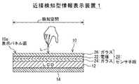
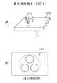
まず、この発明に適用できる近接検知型情報表示装置を説明する。図1はこの近接検知型情報表示装置1の本体部分である表示パネル10の概念を示す要部の断面図であり、図2はその平面図である。 First, a proximity detection type information display device applicable to the present invention will be described. FIG. 1 is a cross-sectional view of a main part showing the concept of a
この表示パネル10は、表示手段として二次元表示手段12を有する。二次元表示手段12としては液晶表示素子(LCD)や、有機EL素子、プラズマディスプレー素子などが考えられる。表示パネル10としては携帯型や据え置き型などに応じてその表示サイズが決定される。この例では、15〜20インチの大きさのLCDを用いた場合である。 The
二次元表示手段12の裏面には保護板14が貼着され、その表面側にはセンサ手段20が設けられる。センサ手段20は二次元のタッチセンサ(パネルセンサ)として機能するもので、2枚の薄い透明なガラス板(誘電体)24,26によって透明な二次元電極(検知電極)22がサンドイッチされて構成される。 A
二次元電極22はワイヤ電極(透明電極)や、透明な導電層によって形成することができ、この例ではワイヤ電極で構成されている。この二次元電極22は図2に示すように横方向に所定の間隔を保持して多数配列された複数の横電極(横軸用検知電極(ワイヤ電極))22Hと、同じく縦方向に同じ間隔を保持して同数配列された複数の縦電極(縦軸用検知電極(ワイヤ電極))22Vとを有し、これらが交差するようにマトリックス状に配列されて二次元電極22が構成される。 The two-
複数の横電極22Hの共通端子23Hおよび複数の縦電極22Vの共通端子23Vがそれぞれガラス板26の一方より導出され、これら共通端子23H,23Vには位置検知用の所定の高周波信号が後述するように交互に印加される。 A
このように二次元表示手段12とセンサ手段20とで構成された表示パネル10は情報表示手段として機能すると共に、静電容量型のタッチセンサとして機能する。二次元表示手段12に情報信号(画像信号)を供給すれば、その情報が表示され、センサ手段20にタッチすれば、対応する情報の選択や表示処理を実行できる。 As described above, the
この表示パネル10は静電容量型であるから、近接検知型のセンサ手段として機能する。つまり、表示パネル面10aに指先などを接触させることで、接触点における横電極22Hと縦電極22Vの各静電容量値(実際には周波数の変化)から接触点の座標を特定できる。 Since the
これに加えて、この発明では表示パネル面10aの二次元平面上の空間に、対象物であるこの例では指先(特定の物体や移動体でもよい)が対峙したとき、この対峙位置Lが指先の検知空間となる。図3のように表示パネル面10aからある対峙位置Lp以上離れると不感帯空間(非検知空間)となるが、対峙位置Lp以下であるときには、指先の位置をセンスできる感帯空間(検知空間)となる。検知できる空間か否かは、対峙した指先の存在を、静電容量の変化として検知できるかどうかで決まる。静電容量に対する検知感度が高ければそれだけ対峙位置Lpを大きく設定できる。 In addition, in the present invention, when a fingertip (which may be a specific object or a moving body) is a target object in the space on the two-dimensional plane of the
検知空間は、検知電極の間隔によって相違する。検知電極として実際に寄与する電極間隔が広いとそれだけ広い検知空間を検知できる。この電極間隔は用途に応じて相違する。電極間隔が狭いときには、5〜10cm程度の検知空間となるが、電極間隔が広くなると1m程度の検知空間まで可能である。上述の例のように、小型で携帯型の表示装置に適用する場合を想定すると、一応5〜10cmの対峙距離Lpが検知空間となるように設計されている。 The detection space differs depending on the interval between the detection electrodes. If the electrode interval that actually contributes as the detection electrode is wide, a detection space wide as much can be detected. This electrode interval varies depending on the application. When the electrode interval is narrow, the detection space is about 5 to 10 cm. However, when the electrode interval is wide, a detection space of about 1 m is possible. Assuming the case where it is applied to a small and portable display device as in the above-described example, it is designed so that a confronting distance Lp of 5 to 10 cm becomes a detection space.
指先の空間位置は、表示パネル面10aに指が接触する接触点までの間であれば連続的に計測できるのが好ましい。この例では、便宜上この検知空間を距離Lに応じて幾つかに分類する。第1の検知空間Iは対峙距離Lq以上でLp以下の空間を指す。対峙距離Lp=10cmであるときの対峙距離Lqは5cm程度に選定される。 It is preferable that the spatial position of the fingertip can be continuously measured as long as it is between the contact point where the finger contacts the
次に、対峙距離がLqからゼロ直前までの空間位置を第2の検知空間IIとする。そして、この例では表示パネル面10aへの接触点が第3の検知空間(検知点)IIIとなる。 Next, a spatial position from the opposite distance Lq to immediately before zero is defined as a second detection space II. In this example, the contact point with the
さて、検知すべき空間位置は検知分解能(検知位置分解能)によって決まる。検知分解能は一般的には検知電極の間隔によって決まる。検知電極の間隔が細かくなるにつれ検知分解能が高くなる。従来ではこの検知分解能は固定されている。 Now, the spatial position to be detected is determined by the detection resolution (detection position resolution). The detection resolution is generally determined by the distance between the detection electrodes. As the interval between the detection electrodes becomes smaller, the detection resolution becomes higher. Conventionally, this detection resolution is fixed.
この発明では、検知すべき空間位置は、表示パネル面10aの面内を含めた表示パネル面10a上の空間である。空間の場合、その空間位置に指先があれば二次元平面での静電容量が相違することになるが、空間位置を正確に表示パネル面10aの二次元平面に投影し、その投影点を検知点として検知する必要性も乏しい。投影点を含むある程度のエリアが検知できれば充分と言える場合が多いからである。 In the present invention, the spatial position to be detected is a space on the
このように投影点近傍を検知するには検知分解能をあまり高くする必要がないが、実際に表示パネル面10aへの接触点を検知するには検知分解能は少なくとも電極間隔やそれ以下であることが好ましい。 As described above, it is not necessary to increase the detection resolution so much to detect the vicinity of the projection point. However, in order to actually detect the contact point on the
このようなことを考慮すると、空間位置に応じた検知分解能を選択できた方が好ましい。連続的に検知分解能を制御するまでもないので、そのような場合には図3のような空間位置に対応した検知分解能に切り替えられる構成とすればよい。つまり段階的に検知分解能を調整できればよい。 In consideration of this, it is preferable that the detection resolution corresponding to the spatial position can be selected. Since it is not necessary to continuously control the detection resolution, in such a case, it may be configured to be switched to the detection resolution corresponding to the spatial position as shown in FIG. In other words, it is sufficient that the detection resolution can be adjusted step by step.
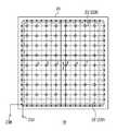
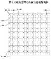
図3の場合では、検知空間I〜IIIに応じて3段階に検知分解能が切り替えられる。センサ手段20を構成する横電極22Hおよび縦電極22Vの数を間引くことで、検知分解能を切り替えることができる。 In the case of FIG. 3, the detection resolution is switched in three stages according to the detection spaces I to III. The detection resolution can be switched by thinning out the number of the
最も検知分解能が高いのは、隣接する検知電極の間隔を検知できることである。この場合には、最小検知エリアが検知電極の電極間隔となり、図4のように検知すべき座標点(○印で表示)が最も密な状態となっている。以下最高検知分解能と言う。 The highest detection resolution is that an interval between adjacent detection electrodes can be detected. In this case, the minimum detection area is the electrode interval between the detection electrodes, and the coordinate points to be detected (indicated by circles) are in the most dense state as shown in FIG. The maximum detection resolution is referred to below.
次に検知分解能が高いのは、検知電極を幾つか電気的に間引いた状態となっているときである。例えば、図5のように1本置きの横電極22Hと縦電極22Vによってセンサ手段20が構成されている場合である。この場合には最小検知エリアが4倍に拡張されたこととなり、それだけ検知分解能が低くなっている。以下この検知分解能を中間検知分解能と言う。検知電極として寄与する検知電極数の間引きは、電気的な処理によって実現できる。 Next, the detection resolution is high when several detection electrodes are electrically thinned out. For example, as shown in FIG. 5, the sensor means 20 is composed of every other
そして、さらに間引く検知電極の電極数を多く、例えば図6に示すように3本置きの検知電極のみによってセンサ手段20を構成することで、図5よりもさらに最小検知エリアが広がった状態となる。これによって検知分解能は最も低い状態(最小検知分解能と言う)となる。 Further, the number of detection electrodes to be thinned out is further increased. For example, as shown in FIG. 6, the sensor means 20 is constituted by only every third detection electrode, so that the minimum detection area is further expanded as compared with FIG. . As a result, the detection resolution becomes the lowest state (referred to as the minimum detection resolution).
したがって、対象物(指先)が表示パネル面10aの面内に次第に近づくときには、検知分解能を最高検知分解能から次第に最低検知分解能となるように対象物の対峙距離に応じて順次切り替えることで、検知エリアを徐々に狭めることができる。 Therefore, when the object (fingertip) gradually approaches the surface of the
検知分解能調整手段は、対象物との間の静電容量の変化を検知することで分解能の調整を行う。具体的には後述するように静電容量の変化を周波数の変化に変換し、この周波数の変化を電圧に変換して得た検出電圧の大小に基づいて検知分解能が調整される。 The detection resolution adjusting means adjusts the resolution by detecting a change in capacitance with the object. Specifically, as will be described later, the detection resolution is adjusted based on the magnitude of the detection voltage obtained by converting a change in capacitance into a change in frequency and converting the change in frequency into a voltage.
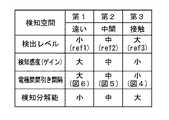
ところで、検知感度は指先などが表示パネル面10aつまりガラス板26の表面(図4の×印)に接触したとき(第3の検知空間III)が最も高いので、接触点Sから得られる出力電圧も最高となる。図4のように接触点Sを中心にしたトータル6本の検知電極例えば横電極a〜fの各出力電圧は図7Cのように、接触点Sが最大レベルでそれを中心に次第に低下した出力特性となる。この検出レベルの大小を検出することで接触点Sを特定できる。 By the way, the detection sensitivity is highest when the fingertip or the like is in contact with the
第2の検知空間IIの場合には、図5に示すような電極間隔となり、指先は表示パネル面10aに接触していないので、指先の真下付近(表示パネル面10aへの指先の投影点近傍)の横電極a〜fから得られる出力電圧もその分低下する(例えば図7B参照)。検出レベルが低下してもそのうちの最大値は、投影点に近い横電極から出力されるので、この出力レベルの差によって投影点を含むエリアを検知できる。 In the case of the second detection space II, the electrode spacing is as shown in FIG. 5 and the fingertip is not in contact with the
さらに、第1の検知空間Iの場合には図6のような電極間隔となることから、指先を表示パネル面10aに投影した投影点近傍の横電極a〜fから得られる出力電圧もさらに低下し、図7Aのような出力レベル関係となる。 Furthermore, in the case of the first detection space I, since the electrode spacing is as shown in FIG. 6, the output voltage obtained from the lateral electrodes a to f in the vicinity of the projection point where the fingertip is projected onto the
その結果、検知空間に拘わらず検知感度を一定にした場合には、検知距離が最も離れている第1の検知空間Iにおける検知が難しくなる傾向にある。第1の検知空間Iでも充分な出力電圧が得られて指先の位置を検知できるようにするには、検知感度を高めればよい。しかしそうすると、今度は指先が表示パネル面10aに近づくにつれ、電極の検知間隔が狭くなるため、検知感度が高くなり、それに比例して出力電圧も高くなるから、発振を起こしてしまう。したがって、理想的には検知感度も検知空間に応じて制御した方が好ましい。 As a result, when the detection sensitivity is constant regardless of the detection space, detection in the first detection space I having the longest detection distance tends to be difficult. In order to obtain a sufficient output voltage in the first detection space I so that the position of the fingertip can be detected, the detection sensitivity may be increased. However, in this case, as the fingertip approaches the
検知空間に対する検出レベル、検知感度および検知分解能(電極間引き間隔)の関係を整理すると図8のようになる。 FIG. 8 shows the relationship between the detection level, detection sensitivity, and detection resolution (electrode thinning interval) with respect to the detection space.
指先が第1の検知空間I内の空間にあるときの検知レベルを第1のスレショールドレベル(ref1)と比較する。検知感度の初期値は最大値(最大ゲイン)に設定され、同様に電極間引き間隔を最も大きくして、検知分解能が一番低く目(最小)に設定されている。指先が第1の検知空間I内にある状態で検知を行うと、そのときの検出レベルは最小となるはずである。 The detection level when the fingertip is in the space within the first detection space I is compared with the first threshold level (ref1). The initial value of the detection sensitivity is set to the maximum value (maximum gain). Similarly, the electrode thinning interval is maximized, and the detection resolution is set to the lowest (minimum). If detection is performed with the fingertip in the first detection space I, the detection level at that time should be minimized.
指先は第1から第2の検知空間に近づくので、第2の検知空間IIに移るときの検出レベルのスレショールドレベルを(ref2)に定める。この第2のスレショールドレベルref2を検出レベルが超えたとき、指先は第2の検知空間II内に近づいたと判断する。検出レベルが大きくなるので、検知感度は逆に中レベルとなるようにゲイン調整される。同時に電極の間引き間隔を減らして今度は検知分解能を高め、中レベルに切り替える。 Since the fingertip approaches from the first detection space to the second detection space, the threshold level of the detection level when moving to the second detection space II is defined as (ref2). When the detection level exceeds the second threshold level ref2, it is determined that the fingertip has approached the second detection space II. Since the detection level increases, the gain is adjusted so that the detection sensitivity becomes the middle level. At the same time, the electrode thinning interval is reduced to increase the detection resolution and switch to the medium level.
この状態で指先の軌跡を検知する。そして、指先が最終的に表示パネル面10aに接触する第3の検知空間IIIまで到達すると、そのときの検出レベルは第3のスレショールドレベル(ref3)を超える。第3のスレショールドレベル(ref3)を超えると、検知感度は最小となるようにゲインの調整が行われ、同時に電極の間引き処理を中止して検知分解能を最大にした状態で接触点の検出が行われることになる。 In this state, the locus of the fingertip is detected. When the fingertip finally reaches the third detection space III in contact with the
こうすることで、表示パネル面10aの二次元平面からこの二次元平面を含む所定の空間内に存在する指先(対象物)の位置を確実に検知できる。 By doing so, the position of the fingertip (object) existing in a predetermined space including the two-dimensional plane can be reliably detected from the two-dimensional plane of the
図9はこのような検知処理を実現するための近接検知型情報表示装置における処理ブロック30の一例を示す。 FIG. 9 shows an example of a
この例では、接触点および投影点の検知は横電極22Hと縦電極22Vとに分けて行なわれ、それぞれから得られた検出値に基づいて接触点や投影点が検出される。 In this example, the contact point and the projection point are detected separately for the
複数の電極で構成された横電極22Hに関する等価回路220Hは、図示するようにインダクタンスLH、抵抗RH、容量CHで構成された発振回路(分布常数回路)と解される。指先の位置(接触点および投影点)によって容量CHの値が変化する。この変化を周波数fhの変化として検出する。周波数fhは、
fh=1/(2π√(LH・CH)) ・・・・(1)
で求められる。The
fh = 1 / (2π√ (LH · CH)) (1)
Is required.
縦電極22Vに関する等価回路220Vも同様な発振回路(分布常数回路)であって、指先の位置による容量CVの変化が周波数fvの変化として求められる。 An
バイアス源32Hと直列接続された交流信号源34Hが駆動源として第1のスイッチ36Hを介して横電極用等価回路220H(実際には横電極22H)の共通端子23Hに接続される。横電極用等価回路220Hにおける周波数fhは、上述したように指先の位置(接触点および投影点)によって変化する。 An
求められた周波数fhは、周波数・電圧変換回路(F・V変換回路)40Hに供給されて、周波数fhの値に応じた電圧に変換される。このF・V変換回路40Hはゲイン調整機能も併せ持つ。このゲインを調整することで結果的に横電極22H側の検知感度を調整できる。変換後の電圧(検出電圧)VhはCPUなどで構成された制御部50に供給される。 The obtained frequency fh is supplied to a frequency / voltage conversion circuit (F / V conversion circuit) 40H and converted into a voltage corresponding to the value of the frequency fh. The F /
縦電極22Vに関しても同様な検出系が設けられている。そのため、バイアス源32Vと直列接続された交流信号源34Vが第2のスイッチ36Vを介して縦電極用等価回路220V(実際には縦電極22V)の共通端子23Vに接続される。 A similar detection system is provided for the
求められた周波数fvは、周波数・電圧変換回路(F・V変換回路)40Vに供給されて、周波数fvの値に応じた電圧に変換される。このF・V変換回路40Vはゲイン調整機能も併せ持つ。このゲインを調整することで結果的に縦電極22V側の検知感度を調整できる。変換後の電圧(検出電圧)Vvは制御部50に供給される。 The obtained frequency fv is supplied to a frequency / voltage conversion circuit (F / V conversion circuit) 40V and converted into a voltage corresponding to the value of the frequency fv. The F /
横電極用等価回路220Hと縦電極用等価回路220Vの各周波数fh,fvを交互に求めるため、制御部50では、第1および第2のスイッチ36H、36Vを交互にスイッチングするためのスイッチング信号が生成される。また、制御部50からは、F・V変換回路40H、40Vに対するゲイン調整のための制御信号Sgが生成され、同時に同量だけゲインの調整が行われる。このゲイン調整と同時に検知分解能の切り替えも行われる。 In order to alternately obtain the frequencies fh and fv of the
制御部50に関連して設けられたメモリ手段(例えばROM)52には、上述した検出処理や各種の表示処理を実行するための複数の処理プログラムが格納されている。また、制御部50によって表示手段12の表示状態が制御されるが、この表示手段12にはGUI(Graphic User Interface)54からのGUI信号が供給され、所定の表示モードが実行される。 A memory means (for example, ROM) 52 provided in association with the
上述した検出処理の実行手順例(情報表示方法)を図10を参照して説明する。
図10に示すフローチャートにおいては、まず操作者の指先(対象物)の接近が検知される(ステップ60)。その検出レベルが基準値(第1のスレショールドレベル(ref1))以上になると、次のステップ61に進み、検知電極の電極間隔を狭めて検知分解能が切り替えられると共に、検知感度の調整が行われる。この状態で指先の軌跡がトレースされる。指先の軌跡をトレースするのは、表示手段12の表示画像をトレース信号に基づいてその表示状態を制御するためである。An example of an execution procedure (information display method) of the detection process described above will be described with reference to FIG.
In the flowchart shown in FIG. 10, first, the approach of the fingertip (object) of the operator is detected (step 60). When the detection level becomes equal to or higher than the reference value (first threshold level (ref1)), the process proceeds to the next step 61, the detection resolution is switched by narrowing the electrode interval of the detection electrodes, and the detection sensitivity is adjusted. Is called. In this state, the trace of the fingertip is traced. The trace of the fingertip is traced in order to control the display state of the display image of the
続いて、ステップ62において検出レベルがチェックされ、基準値(第2のスレショールドレベル(ref2))を超えたときには、検知電極の間隔が狭くなるように調整されると共に、検知感度が低くなるように調整される(ステップ63)。このときも指先の軌跡がトレースされ、そのトレース信号に基づいて表示画像の制御が行われる。 Subsequently, in
そして検出レベルが基準値(第3のスレショールドレベル(ref3))を超えたときには(ステップ64)、最小の電極間隔に調整して最大の検知分解能とすると共に、検知感度を最も低めに設定しながら、表示パネル面10aに接触した状態にある指先の軌跡をトレースする(ステップ65)。指先が表示パネル面10aに接触した状態で表示パネル面10aの表面をなぞることも考えられ、その場合にも表示状態を制御することが考えられるからである。 When the detection level exceeds the reference value (the third threshold level (ref3)) (step 64), the minimum electrode interval is adjusted to obtain the maximum detection resolution and the detection sensitivity is set to the lowest. Meanwhile, the trajectory of the fingertip in contact with the
ステップ65の状態でさらに検出レベルがチェックされ、この検出レベルが逆に基準値(第3のスレショールドレベル(ref3))を下回ったときには(ステップ66)、指先が表示パネル面10aから離れたことになるので、この場合には電極間隔および検知感度をステップ63の状態に戻して検出処理を続行する(ステップ67)。 In the state of
ステップ67の状態で、検出レベルが再びチェックされ、この検出レベルが基準値(第2のスレショールドレベル(ref2))を下回ったときには(ステップ68)、表示パネル面10aの検知空間IIより指先が離れた状態にあるので、この場合には電極間隔を最大幅に戻して検知分解能を初期値に戻す。そして、検知感度も最大値(初期値)に戻して指先の接近状態が検知されることになる(ステップ60)。 In the state of step 67, the detection level is checked again, and when this detection level falls below the reference value (second threshold level (ref2)) (step 68), the fingertip from the detection space II on the
ステップ62において、検出レベルが基準値(ref2)を下回ったときは指先が表示パネル面10aより離れたことを意味するものであるから、この場合にはステップ60に遷移する。また、ステップ64において、検出レベルが基準値(ref3)を下回ったときには、表示パネル面10aより指先が離れたことになるので、この場合にはステップ62に遷移し、同様にステップ66において検出レベルが基準値(ref3)を下回ったときも、表示パネル面10aより指先が離れたことになるので、この場合にもステップ62に遷移する。 In
続いて、この発明に係る近接検知型情報表示装置1における表示処理例を説明する。上述したように表示パネル面10a上における指先の空間位置を検知できるので、この空間位置や指先の動きさらにはその軌跡に基づいて、表示手段12に表示された情報(画像)の表示状態が制御される。 Next, an example of display processing in the proximity detection type
そのため、この近接検知型情報表示装置1は、映像情報を表示する表示手段の他に、この表示手段の表面に設けられた複数の検知電極から構成される静電容量型センサ手段、検知電極の出力を制御する電極出力制御手段、検知電極の動作・非動作を管理する電極動作管理手段を有する。 For this reason, the proximity detection type
そして、静電容量型センサ手段によって対象物が検知できない場合には、電極出力制御手段は検知電極の出力を最大にすると共に、電極動作管理手段では、検知電極の検知間隔が最大となるような処理を行う。静電容量型センサ手段によって対象物が検知できた場合には、対象物と検知電極との対向距離に応じて、電極出力制御手段は検知電極の出力を下げると共に、電極動作管理手段では、検知電極の検知間隔が狭くなるような処理を行う。 When the object cannot be detected by the capacitive sensor means, the electrode output control means maximizes the output of the detection electrode, and the electrode operation management means maximizes the detection electrode detection interval. Process. When the object can be detected by the capacitive sensor means, the electrode output control means reduces the output of the detection electrode according to the facing distance between the object and the detection electrode, and the electrode operation management means detects the object. Processing is performed to reduce the electrode detection interval.
したがって、このような検出処理や表示処理を行うため、制御部50は少なくとも以下の処理ステップを有する。
(1)センサ手段20に対する接触点と表示パネル面10aと対向する空間点をそれぞれ検知するステップ
(2)表示パネル面10aからの検知位置によって、検知すべき検知分解能を調整するステップ
(3)同じく検知感度を調整するステップ
(4)空間点上における検知軌跡に応じて、表示手段12に表示される映像情報の大きさ、動き、回転方向などの表示状態を制御するステップ
続いて、表示手段12に表示された画像の表示処理例を説明する。以下に述べる表示制御は、何れも図9のメモリ手段52に保存された表示制御プログラムのうち、特定の表示制御プログラムが選択されて起動されている状態での表示制御例である。Therefore, in order to perform such detection processing and display processing, the
(1) A step of detecting a contact point with respect to the sensor means 20 and a spatial point opposite to the
(表示制御例I)
図11に示す例は、第1の検知空間Iにおいて指先が検知されると、画面の表示モードに切り替わり、画面全体が僅かに明るくなるように表示状態が制御される(図11A1,A2)。これは例えばスリープモードからの制御モードの一例である。(Display control example I)
In the example shown in FIG. 11, when a fingertip is detected in the first detection space I, the display mode is switched to the screen display mode, and the display state is controlled so that the entire screen is slightly brightened (FIGS. 11A1 and A2). This is an example of a control mode from the sleep mode, for example.
指先が表示パネル面10aに接近して第2の検知空間II内で指先が検知されると、今度は指先の周囲に光が集光されるように表示状態が制御される(図11B1,B2)。そして、指先が表示パネル面10aに接触すると光点がポインタ表示に切り替えられる(図11C1,C2)。 When the fingertip approaches the
このように図11の例は、予め特定のアプリケーションソフトが起動されており、スリープモードに切り替わった状態のときに応用できる、指先の動きに基づく表示制御例である。 As described above, the example of FIG. 11 is a display control example based on the movement of the fingertip, which can be applied when specific application software is activated in advance and is switched to the sleep mode.
(表示制御例II)
(その1)
図12は、画面の左右両側に複数のアイコン(○印)が表示されている状態で、例えば指先が第1の検知空間I内に入ったことが検知されると、両脇に表示されていた複数のアイコンが画面の中心を原点とする円周上に配列されるように制御される表示制御例である。そして、特定のアイコンの位置を接触点とすることで、そのアイコンに関連したアプリケーションソフトが起動される例である。(Display control example II)
(Part 1)
FIG. 12 shows a state where a plurality of icons (circles) are displayed on both the left and right sides of the screen. For example, when it is detected that the fingertip has entered the first detection space I, the icons are displayed on both sides. This is a display control example in which a plurality of icons are controlled so as to be arranged on a circle having the center of the screen as the origin. And it is an example by which the application software relevant to the icon is started by setting the position of a specific icon as a contact point.
(その2)
図13は、図12のように画面の中心を原点とする円周上に配列表示されている複数のアイコン(○印)が、第2の検知空間II内で指先を回転させることで、指先の回転方向と回転速度に同期して同じ方向(矢印図示)に回転するように制御される表示制御例である。(Part 2)
FIG. 13 shows a plurality of icons (circles) arranged on the circumference with the center of the screen as the origin as shown in FIG. 12 by rotating the fingertip in the second detection space II. This is a display control example that is controlled to rotate in the same direction (shown by an arrow) in synchronization with the rotation direction and the rotation speed.
(その3)
図12の表示状態で、第2の検知空間II内に移るように、特定のアイコンを目指して指先を近づけると(図14A)、この特定のアイコンを含む前後3つのアイコンが、拡大表示されながら画面の中心から放射状に表示される表示制御例である(図14B)。このとき指先はアイコンの中心に位置する。(Part 3)
In the display state of FIG. 12, when the fingertip is moved closer to a specific icon so as to move into the second detection space II (FIG. 14A), the three icons before and after the specific icon are enlarged and displayed. It is a display control example displayed radially from the center of the screen (FIG. 14B). At this time, the fingertip is positioned at the center of the icon.
(その4)
図15は、図12の表示状態のとき、指先を回転させるとその方向にアイコンが回転する表示制御例であって、これによって操作者が最も操作し易い表示位置にアイコンを表示させることができる(図15A,B)。(Part 4)
FIG. 15 is an example of display control in which the icon rotates in the direction when the fingertip is rotated in the display state of FIG. 12, whereby the icon can be displayed at a display position that is most easily operated by the operator. (FIGS. 15A and 15B).
(その5)
図15の状態で、特定のアイコンを選択し易くその表示位置を変更した段階で、指先を特定のアイコンが表示されている表示パネル面10aに接触させると、特定のアイコンのみが表示され(図16A,B)、そのアイコンは指先に収束するように表示制御される(図17A,B)。(Part 5)
In the state of FIG. 15, when the specific icon is easily selected and its display position is changed, when the fingertip is brought into contact with the
このように、指先の空間位置を検知すると共に、その軌跡をトレースすることで、今までには経験し得なかったインタラクティブな表示状態を実現できる。 Thus, by detecting the spatial position of the fingertip and tracing the trajectory, an interactive display state that could not be experienced before can be realized.
(その他の表示制御例)
図示はしないが、(表示制御例II)に類似するものとして、次のような表示制御も可能である。例えば、指先の空間位置を検知できる対峙間隔内(第1の検知空間I)に近づくと、二次元表示手段12には特定のメニュー画面が表示される。第1の検知空間I内を指先が移動、例えば指先が回転すると回転方向と回転速度に応じた方向と速度でメニュー画面が回転する。回転させることに特に意味があるのではない。(Other display control examples)
Although not shown, the following display control is also possible as similar to (Display Control Example II). For example, a specific menu screen is displayed on the two-
指先が第1の検知空間Iより表示パネル面10aに近づき第2の検知空間II内の存在が確認されると、メニュー画面が拡大表示され、一部のメニュー項目の画像のみが表示される。その状態で指先を動かすとその軌跡に応じてメニュー項目の画像が動く。そして、最終的に特定のメニュー項目が表示された表示パネル面10aに接触する(第3の検知空間III)と、その接触点に表示されたメニュー項目が選択される。このようなインタラクティブな表示制御も可能になる。 When the fingertip approaches the
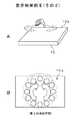
上述した実施例では、検知電極26としては透明なワイヤ電極26H,26Vをマトリックス状に配列して使用した。このワイヤ電極26H,26Vに代わるものとして点電極がある。図18に点電極28を使用したときの表示パネル10の平面構成例を示す。 In the embodiment described above, transparent wire electrodes 26H and 26V are used as the
点電極28を使用する場合、縦横に配列されたワイヤ電極の交点の位置に、点電極28が配置される。図18はm行n列の例である。点電極28を使用した場合の断面例を図19に示す。 When the
表示手段12としては液晶表示素子の他に、有機EL表示素子などの透明な二次元表示素子を使用することができる。図19以下の例は、透明な有機EL表示素子を使用した場合である。表示手段12の表面にはセンサ手段20が貼着される。 As the display means 12, a transparent two-dimensional display element such as an organic EL display element can be used in addition to the liquid crystal display element. The example in FIG. 19 and subsequent figures is a case where a transparent organic EL display element is used. Sensor means 20 is attached to the surface of the display means 12.
センサ手段20は一対のガラス基板24,26によって点電極(実際は点電極群)28が挟持された構成を採る。点電極28は静電容量型センサとして機能させるため、可変型の発振器として構成される。点電極28は全て同じ構成であるため、点電極28A1についてその構成を説明する。 The sensor means 20 adopts a configuration in which a point electrode (actually a point electrode group) 28 is sandwiched between a pair of
点電極28A1は図20に示すように、ガラス基板24上に取り付けられたこの例では、チップ型のコイル80とコンデンサ81が導電層82によって並列接続されて共振回路が構成されると共に、この例ではコンデンサ81に近接してチップ型の発振器85が設けられ、全体として可変型の発振器となされる。発振器85は水晶振動子やセラミック振動子とその増幅回路を備えている。発振器85には所定長の導電層86が接続される。 As shown in FIG. 20, the point electrode 28A1 is mounted on the glass substrate 24. In this example, a chip-
また、並列接続点pから引き出し用の導電層83A1が導出され、センサ手段20の端部に設けられた出力端子84A1に接続される。発振器85には動作電圧を供給するため、電圧端子88A1から所定の動作電圧が導電層87A1を介して供給される。 In addition, a lead conductive layer 83A1 is led out from the parallel connection point p and connected to an output terminal 84A1 provided at an end of the sensor means 20. In order to supply an operating voltage to the
他の点電極28A2,28B1,28B2,・・・に関しても同じように構成され、そして全ての点電極28から出力端子84(84A1,84A2,・・・)が導出される。全ての点電極28には同じ動作電圧が印加されるから、電源端子88(88A1,88A2,・・・)は共通の電源端子となる。 The other point electrodes 28A2, 28B1, 28B2,... Are configured in the same manner, and output terminals 84 (84A1, 84A2,...) Are derived from all the
このように構成した場合、導電層86と並列接続用の導電層82とがそれぞれアンテナとして機能して、発振器85とコイル80およびコンデンサ81が相互に電気的に接続される。 When configured in this manner, the
その結果、点電極28A1は発振器として動作すると共に、ガラス基板26つまり表示パネル10aと対向する指の位置によって、コンデンサ81の容量が変化することから、指の位置によって発振周波数fhも変化する。つまり、点電極28A1は周波数可変型の発振器として機能する。基準の発振周波数foは、振動子の発振周波数である。 As a result, the point electrode 28A1 operates as an oscillator, and the capacitance of the
なお、図20において鎖線で示したエリア89は隔壁板であって、点電極28の大きさを示すと共に、隣接する点電極28に発振出力が不要輻射されないようにするためのバリアとして機能する。この隔壁板89によって隣接する点電極28が互いに干渉することなく独立して指の接近・離間および接触を検知できる。
図20において、導電層82と86は接続することもできる。An
In FIG. 20, the
図18に示す表示装置10にあっても、指の接近・離間および接触に応じて、検知分解能が切り替える。図18は第3の検知空間IIIのときの検知電極であって、最小電極間隔である。 Even in the
第2の検知空間IIであるときは、電極数の間引き(電気的間引き)が行われて、例えば図21のように一つおきの電極が検知電極として使用される。そして、第1の検知空間Iとなったときは、さらに間引きが行われて、例えば図22のように2つおきの電極が検知電極として使用されるようにして検知分解能の調整が行われる。 In the case of the second detection space II, the number of electrodes is thinned out (electrical thinning), and every other electrode is used as a detection electrode, for example, as shown in FIG. When the first detection space I is reached, further thinning is performed, and the detection resolution is adjusted so that every second electrode is used as a detection electrode, for example, as shown in FIG.
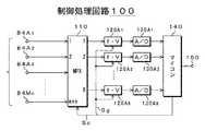
図23はこのように構成された表示装置10の制御処理回路100の一例を示す要部の系統図である。上述したように点電極群は、m×n個で構成される。図18の場合、m=n=18である。このように多数の点電極のそれぞれから導出された出力端子28A1〜28Mnはマルチプレクサー(MPX)110の入力端子に接続され、出力端子28A1〜28Mnに得られた周波数成分がマルチプレクサー(MPX)110に供給される。マルチプレクサー110には、p×q=r個の周波数・電圧変換回路120A1〜120Arが接続される。ここに、m×n≫ rであって、この例はr=9の場合である。 FIG. 23 is a system diagram of a main part showing an example of the
マルチプレクサー110では入力側を高速に順次切り替える、つまり高速走査することで、入力数よりも大幅に少ない出力段の周波数・電圧変換回路120に、該当する点電極からの周波数成分を割り振っている。r=9であるので、最大2列分の全ての点電極から得られる周波数成分が、1台の周波数・電圧変換回路120で順次処理される。 The
つまり、検知分解能が最も高いとき(第3の検知空間III)で、2列分である(2×18)個の点電極数を1台の周波数・電圧変換回路120で取り扱い、次に検知分解能が高いとき(第2の検知空間II)は、同じく2列分のうち、間引かれた(2×9)個の点電極数を1台の周波数・電圧変換回路120で取り扱い、最も検知分解能が低い第1の検知空間Iのときは、2列分のうち最初の1列分であって1/4に間引かれた6個の点電極数を1台の周波数・電圧変換回路120で取り扱うことになる。この高速切り替えによる変換処理によって、全ての点電極からの情報を少ない回路数で電圧に変換できる。 That is, when the detection resolution is the highest (third detection space III), the number of (2 × 18) point electrodes corresponding to two rows is handled by one frequency / voltage conversion circuit 120, and then the detection resolution Is high (second detection space II), the same number of thinned (2 × 9) point electrodes in two rows are handled by one frequency / voltage conversion circuit 120, and the highest detection resolution When the first detection space I is low, the number of the six point electrodes that are thinned out to ¼ of the first one of the two rows is reduced by one frequency / voltage conversion circuit 120. It will be handled. By this conversion process by high-speed switching, information from all point electrodes can be converted into a voltage with a small number of circuits.
これら周波数・電圧変換回路120はゲイン調整機能も併せ持ち、検知空間に応じて出力ゲインが自動調整される。 These frequency / voltage conversion circuits 120 also have a gain adjustment function, and the output gain is automatically adjusted according to the detection space.
周波数成分が電圧に変換された後は、それぞれA/D変換器130A1〜130A8でデジタルデータに変換され、そのデジタルデータがマイコンで構成されたデータ処理部140に供給される。 After the frequency component is converted into voltage, it is converted into digital data by the A / D converters 130A1 to 130A8, respectively, and the digital data is supplied to the
データ処理部140からは上述したマルチプレクサー110に高速切り替え信号Scが供給されると共に、検知空間に応じたゲイン調整信号Sgがそれぞれの周波数・電圧変換回路120に供給される。これによってデータ処理部140では対応する点電極28からの検知情報を順次取得して検知空間や、接触点の特定が行われ、出力端子150に得られるその最終出力(検知出力)が上述した表示手段12への制御信号として供給される。 From the
実施例1では、表示手段12の表面にセンサ手段20を貼り付けた一体型の近接検知型表示装置1にこの発明を適用した。実施例2では表示手段12とセンサ手段20とが別体構成の例である。In the first embodiment, the present invention is applied to the integrated proximity
そのため、実施例2における近接検知型表示装置1は図24のように、センサ手段20と、そのセンサ出力が供給される制御処理回路100と、制御処理回路100からの検知出力が供給される表示手段12とで構成される。表示手段12は便宜的に表示パネルのみを示す。表示手段12には検知出力が直接供給されるのではなく、映像表示処理系(図示はしない)に供給されて、検知出力に応じた制御がなされる。 Therefore, as shown in FIG. 24, the proximity detection
制御処理回路100はセンサ手段20側に一体化するか、表示手段12側に一体化するか、あるいはこれらとは別体に構成することもできる。以下の例は、説明の関係から、別体構成を例示する。また、センサ手段20に使用される検知電極は、透明なワイヤ電極か点電極である。 The
表示パネル12としては、液晶表示素子や有機EL表示素子を使用できるが、非表示状態では裏面側を透視できる透明体で構成された有機EL表示素子を使用した場合を例示する。 As the
続いて、このような別体型の近接検知型表示装置1の用途(使用例)について図25以下を参照して説明する。 Next, an application (usage example) of such a separate proximity
(使用例1)
図25に使用例1を示す。この例は、ショーウインドーに展示や陳列されている商品の宣伝用として近接検知型表示装置1を使用した場合である。そのため、建物200の壁面に設けられたショーウインドー202の前面ガラス(透明ガラス)204のうち、歩行者の接近を検知できる位置にセンサ手段20が配置され、歩行者の目線に合った位置に表示手段12が配置される。(Usage example 1)
FIG. 25 shows a first usage example. In this example, the proximity detection
表示手段12は非表示状態では裏面側を透視できるので、表示手段12によってショーウインドー202内の展示品(陳列品)が見えなくなるようなおそれはない。 Since the display means 12 can be seen through the back side in the non-display state, there is no possibility that the display means 12 will not allow the display items (display items) in the
また、歩道側を歩いている歩行者の接近を検知し易くするため、前面ガラス204の中央より下側に図26のようにセンサ手段20が配置され、その上段の適当な位置に表示手段12が配置される。 Further, in order to make it easy to detect the approach of a pedestrian walking on the sidewalk side, the sensor means 20 is arranged below the center of the
歩行者の接近を容易に検知できるようにするため、センサ手段20を構成する点電極の最小間隔が比較的広目に設定されている。この例では、10〜20cm程度で、その個数も10個程度マトリックス状に配置されて構成される。こうすれば、第1の検知空間Iとしては40〜80cm程度まで拡張できるので、歩行者が意識してショーウインドー202に接近するのを十分検知できる。第2の検知空間IIは20〜40cm程度となる。 In order to make it possible to easily detect the approach of a pedestrian, the minimum interval between the point electrodes constituting the sensor means 20 is set to be relatively wide. In this example, it is about 10 to 20 cm, and the number is about 10 arranged in a matrix. In this way, the first detection space I can be expanded to about 40 to 80 cm, so that it can be sufficiently detected that the pedestrian is consciously approaching the
そして、歩行者が第1の検知空間Iに接近したことを検知すると、表示手段12に展示されている商品(ウエアなど)の紹介映像を表示する。合わせて音声による商品紹介も行う。そして、さらに第2の検知空間IIに接近したときには、その商品の内容がよく分かる映像に切り替え、センサ手段20に歩行者の手が触れたときには、該当商品の値段など、顧客にあった映像に切り替える。このような映像制御を行うことで、インタラクティブな表示を実現できる。 When it is detected that the pedestrian has approached the first detection space I, an introductory image of a product (such as wear) displayed on the display means 12 is displayed. At the same time, we will introduce products by voice. When the second detection space II is further approached, the image is switched to an image that allows the contents of the product to be well understood, and when the pedestrian's hand touches the sensor means 20, the image of the product such as the price of the corresponding product is displayed. Switch. By performing such video control, interactive display can be realized.
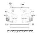
近接検知型表示装置1をショーウインドー202に適用した場合、歩行者は建物200の左右何れかから近づいてくるか分からない。そのような場合、特にショーウインドー202の展示面積が広いようなときには、図27のようにショーウインドー202の前面ガラス204の左右両端に近い側に、それぞれ近接検知型表示装置1を配置することもできる。 When the proximity
こうすれば、どちらの方向からショーウインドー202に近づいても、歩行者の接近を確実かつ素早く検知できるし、歩行者が複数いても対応できる。図27の変形例として図28のように表示手段12を共通にし、センサ手段20のみ左右に配置することも可能である。 In this way, the approach of the pedestrian can be detected reliably and quickly regardless of the direction from which the
図29は、この発明を透明ガラスを使用した自動ドアに適用した場合である。最近では、自動ドアに設置されたセンサ部に手を触れることでドアが開閉するタッチ式の自動ドアが増えている。センサ部に手を触れない限りドアは開かないし、透明ガラスであるためガラスの存在を知らずに建物の内部に入ろうとすることも考えられる。 FIG. 29 shows a case where the present invention is applied to an automatic door using transparent glass. Recently, an increasing number of touch-type automatic doors are opened and closed by touching a sensor unit installed on the automatic door. Unless the sensor part is touched, the door does not open, and since it is transparent glass, it may be possible to enter the building without knowing the presence of the glass.
このようなことを考慮して、図29に示す自動ドア210にあっては、タッチセンサ部に代えて上述した近接検知型表示装置1を使用する。近接検知型表示装置1は左右のドア212,214の中央端面近くに設置される。近接検知型表示装置1は表示手段12とセンサ手段20とが一体化された表示装置が使用される。 Considering this, in the automatic door 210 shown in FIG. 29, the proximity detection
ただし、表示手段12としては有機EL表示素子のように透明体の方が意匠的に好ましい。センサ手段20に使用される検知電極としてはワイヤ電極、点電極の何れでもよい。第1の検知空間としては30〜40cmが好ましいので、それに適した電極配列となる。近接検知型表示装置1のサイズは、センサ部よりも若干大きくなる。 However, as the display means 12, a transparent body is preferable in design as in the case of an organic EL display element. The detection electrode used in the sensor means 20 may be a wire electrode or a point electrode. Since 30-40 cm is preferable as the first detection space, an electrode arrangement suitable for the first detection space is obtained. The size of the proximity
近接検知型表示装置1は、警報表示と共にセンサ部として機能させる。そのため、第1の検知空間内に利用者が接近したときには、自動ドア210のガラスがあることを表示手段12に表示してまず警鐘すると共に、センサ手段20にタッチするように勧める表示を行う。音声を併用することも可能である。 The proximity
第2の検知空間内まで近づいたときは例えば、センサ手段20にタッチするように勧める表示のみを行う。音声案内も併用する。そして第3の検知空間であるセンサ手段20への接触を検知すると、表示状態はそのままにしながら、ドアが開く旨の音声案内を行うと共に、ドアを開くような指示を自動ドアの駆動制御部に供給する。これで、ドアが自動的に開く。こうすれば、安全を確認しながらドアの自動開閉を実現できる。 When approaching the second detection space, for example, only a display that recommends touching the sensor means 20 is performed. Voice guidance is also used. When contact with the sensor means 20, which is the third detection space, is detected, the guidance for opening the door is given to the automatic door drive controller while the display state remains unchanged and the door is opened. Supply. This will automatically open the door. In this way, automatic door opening and closing can be realized while ensuring safety.
この発明では、各種の自動販売機やガソリンスタンドのインタフェース画面用の表示装置として、自動車や航空機などの乗り物に装備された制御用パネルの表示装置として、あるいはショーウインドーに設置された商品紹介などに供されるタッチパネル用の表示装置として、自動ドアの開閉用タッチ部兼用の表示素子として、さらにはパソコンなどの表示装置やゲーム機の表示装置などとして適用できる。 In the present invention, it is used as a display device for interface screens of various vending machines and gas stations, as a display device for a control panel mounted on a vehicle such as an automobile or an aircraft, or for introducing a product installed in a show window. As a display device for a touch panel to be used, the present invention can be applied as a display element serving also as a touch unit for opening and closing an automatic door, and further as a display device such as a personal computer or a display device of a game machine.
1・・・近接検知型情報表示装置、10・・・表示パネル、12・・・表示手段(LCD)、20・・・センサ手段、22・・・電極(ワイヤ電極)、220H・・・横電極、220V・・・縦電極、24,26・・・ガラス板、10a・・・表示パネル面、40H、40V・・・F・V変換回路、28(28A、28B)・・・点電極、80・・・チップ型コイル、81・・・チップ型コンデンサ、82,86・・・導電層、85・・・発振器、28・・・点電極、80・・・コイル、81・・・コンデンサ、82,86・・・導電層、85・・・発振回路、100・・・制御処理回路、140・・・データ処理回路、202・・・ショーウインドー、204・・・前面ガラス、210・・・自動ドアDESCRIPTION OF
Claims (13)
Translated fromJapanese複数の検知電極からなるセンサ手段と、
上記センサ手段と上記検知電極に接触する対象物との対向距離によって検知すべき検知分解能が調整される検知分解能調整手段とからなる
ことを特徴とする近接検知型情報表示装置。Display means for displaying video information;
Sensor means comprising a plurality of sensing electrodes;
A proximity detection type information display device comprising: a detection resolution adjusting unit that adjusts a detection resolution to be detected according to a facing distance between the sensor unit and an object in contact with the detection electrode.
ことを特徴とする請求項1記載の近接検知型情報表示装置。2. The proximity detection type information display device according to claim 1, wherein the sensor means is provided on a surface of the display means.
ことを特徴とする請求項1記載の近接検知型情報表示装置。2. The proximity detection type information display device according to claim 1, wherein the display means is a transparent body through which the back side can be seen in a non-display state, and is provided apart from the sensor means.
上記検知電極は、二次元平面にマトリックス状に張られた透明な横軸用ワイヤ電極と、縦軸用ワイヤ電極とで構成される
ことを特徴とする請求項1記載の近接検知型情報表示装置。The sensor means is a capacitance detection type panel sensor,
2. The proximity detection type information display device according to claim 1, wherein the detection electrode is composed of a transparent horizontal axis wire electrode stretched in a matrix on a two-dimensional plane and a vertical axis wire electrode. .
上記検知電極はマトリックス状に配置された複数の点電極で構成される
ことを特徴とする請求項1記載の近接検知型情報表示装置。The sensor means is a capacitance detection type panel sensor,
2. The proximity detection type information display device according to claim 1, wherein the detection electrode is composed of a plurality of point electrodes arranged in a matrix.
これらコイルおよびコンデンサに近接配置されたチップ型の発振器で構成される
ことを特徴とする請求項5記載の近接検知型情報表示装置。The point electrode includes a chip-type coil and a capacitor connected in parallel;
6. The proximity detection type information display device according to claim 5, wherein the proximity detection type information display device is constituted by a chip type oscillator arranged in proximity to the coil and the capacitor.
ことを特徴とする請求項1記載の近接検知型情報表示装置。2. The proximity detection according to claim 1, wherein the detection resolution adjusting means adjusts the detection resolution by adjusting a detection interval of the detection electrodes used as detection electrodes according to the facing distance. Type information display device.
ことを特徴とする請求項1記載の近接検知型情報表示装置。2. The proximity detection type information display device according to claim 1, wherein the detection interval of the detection electrodes is adjusted by thinning out the number of electrodes contributing as the detection electrodes.
ことを特徴とする請求項1記載の近接検知型情報表示装置。2. The proximity detection type information display device according to claim 1, wherein the detection sensitivity of the detection electrode is adjusted together with the adjustment of the detection resolution.
上記対象物の動き又はおよび対向距離に応じて、上記表示手段に表示される映像情報の大きさ、動き、回転方向などが制御される
ことを特徴とする近接検知型情報表示装置。Detection to be detected by a display means for displaying video information, a sensor means composed of detection electrodes provided on the surface of the display means, and a facing distance between the sensor means and an object in contact with the detection electrodes A proximity detection type information display device comprising a detection resolution adjustment means for adjusting resolution,
A proximity detection type information display apparatus, wherein the size, movement, rotation direction, and the like of video information displayed on the display means are controlled in accordance with the movement of the object or the facing distance.
この表示手段の表面に設けられた複数の検知電極から構成される静電容量型センサ手段と、
上記検知電極の出力を制御する電極出力制御手段と、
上記検知電極の動作・非動作を管理する電極動作管理手段とを有し、
上記静電容量型センサ手段によって対象物が検知できない場合には、上記電極出力制御手段は上記検知電極の出力を最大にすると共に、上記電極動作管理手段では、上記検知電極の検知間隔が最大となるような処理を行い、
上記静電容量型センサ手段によって対象物が検知できた場合には、上記対象物と上記検知電極との対向距離に応じて、上記電極出力制御手段は上記検知電極の出力を下げると共に、上記電極動作管理手段では、上記検知電極の検知間隔が狭くなるような処理を行う
ことを特徴とする近接検知型情報表示装置。Display means for displaying video information;
A capacitive sensor means comprising a plurality of detection electrodes provided on the surface of the display means;
Electrode output control means for controlling the output of the detection electrode;
Electrode operation management means for managing the operation / non-operation of the detection electrode,
When the object cannot be detected by the capacitive sensor means, the electrode output control means maximizes the output of the detection electrode, and the electrode operation management means maximizes the detection interval of the detection electrode. Process like
When the object can be detected by the capacitive sensor means, the electrode output control means lowers the output of the detection electrode and reduces the output of the detection electrode according to the facing distance between the object and the detection electrode. The proximity detection type information display device characterized in that the operation management means performs processing such that the detection interval of the detection electrodes is narrowed.
上記センサ手段との対向距離に応じて、上記センサ手段の検知分解能を調整するステップと、
上記対象物の動き又は及び上記センサ手段との対向距離に応じて、上記表示手段に表示される映像情報の大きさ、動き、回転方向などの表示状態を制御するステップと、
からなることを特徴とする近接検知型情報表示装置の情報表示方法。Detecting the facing distance of the sensor unit from the object with the sensor unit associated with the display unit;
Adjusting the detection resolution of the sensor means according to the facing distance to the sensor means;
Controlling the display state such as the size, movement, rotation direction, etc. of the video information displayed on the display means according to the movement of the object or the facing distance from the sensor means;
An information display method for a proximity detection type information display device comprising:
ことを特徴とする請求項12記載の近接検知型情報表示装置の情報表示方法。13. The information display method for a proximity detection type information display device according to claim 12, further comprising a step of adjusting the detection sensitivity of the sensor means together with the adjustment of the detection resolution.
Priority Applications (6)
| Application Number | Priority Date | Filing Date | Title |
|---|---|---|---|
| JP2007233361AJP4766340B2 (en) | 2006-10-13 | 2007-09-07 | Proximity detection type information display device and information display method using the same |
| US13/195,302US8217914B2 (en) | 2006-10-13 | 2011-08-01 | Information display apparatus with proximity detection performance and information display method using the same |
| US13/474,110US8665237B2 (en) | 2006-10-13 | 2012-05-17 | Information display apparatus with proximity detection performance and information display method using the same |
| US14/177,011US9110513B2 (en) | 2006-10-13 | 2014-02-10 | Information display apparatus with proximity detection performance and information display method using the same |
| US14/814,313US9588592B2 (en) | 2006-10-13 | 2015-07-30 | Information display apparatus with proximity detection performance and information display method using the same |
| US15/414,678US9870065B2 (en) | 2006-10-13 | 2017-01-25 | Information display apparatus with proximity detection performance and information display method using the same |
Applications Claiming Priority (3)
| Application Number | Priority Date | Filing Date | Title |
|---|---|---|---|
| JP2006280733 | 2006-10-13 | ||
| JP2006280733 | 2006-10-13 | ||
| JP2007233361AJP4766340B2 (en) | 2006-10-13 | 2007-09-07 | Proximity detection type information display device and information display method using the same |
Related Child Applications (2)
| Application Number | Title | Priority Date | Filing Date |
|---|---|---|---|
| JP2010012821ADivisionJP4688007B2 (en) | 2006-10-13 | 2010-01-25 | Display control apparatus, display control method, and program |
| JP2011043845ADivisionJP5621098B2 (en) | 2006-10-13 | 2011-03-01 | Information processing apparatus and information processing method |
Publications (3)
| Publication Number | Publication Date |
|---|---|
| JP2008117371Atrue JP2008117371A (en) | 2008-05-22 |
| JP2008117371A5 JP2008117371A5 (en) | 2009-12-03 |
| JP4766340B2 JP4766340B2 (en) | 2011-09-07 |
Family
ID=39503202
Family Applications (1)
| Application Number | Title | Priority Date | Filing Date |
|---|---|---|---|
| JP2007233361AExpired - Fee RelatedJP4766340B2 (en) | 2006-10-13 | 2007-09-07 | Proximity detection type information display device and information display method using the same |
Country Status (1)
| Country | Link |
|---|---|
| JP (1) | JP4766340B2 (en) |
Cited By (98)
| Publication number | Priority date | Publication date | Assignee | Title |
|---|---|---|---|---|
| JP2009258903A (en)* | 2008-04-15 | 2009-11-05 | Mitsubishi Electric Corp | Touch panel device |
| JP2009289235A (en)* | 2008-06-02 | 2009-12-10 | Mitsubishi Electric Corp | Touch panel |
| JP2010061224A (en)* | 2008-09-01 | 2010-03-18 | Honda Motor Co Ltd | Input/output device for automobile |
| EP2175351A2 (en) | 2008-10-10 | 2010-04-14 | Sony Corporation | Apparatus, system, method, and program for processing information |
| JP2010092419A (en)* | 2008-10-10 | 2010-04-22 | Sony Corp | Information processing apparatus, method and system, and program for information processing |
| JP2010108255A (en)* | 2008-10-30 | 2010-05-13 | Denso Corp | In-vehicle operation system |
| WO2010055844A1 (en)* | 2008-11-11 | 2010-05-20 | 株式会社フジクラ | Position detector |
| JP2010128545A (en)* | 2008-11-25 | 2010-06-10 | Sony Corp | Information processing apparatus, information processing method, and program for information processing |
| JP2010176190A (en)* | 2009-01-27 | 2010-08-12 | Ntt Docomo Inc | Mode setting system |
| JP2010191574A (en)* | 2009-02-17 | 2010-09-02 | Victor Co Of Japan Ltd | Operation control method using electronic equipment and touch panel |
| JP2010244518A (en)* | 2009-04-03 | 2010-10-28 | Renei Kagi Kofun Yugenkoshi | Method and related apparatus for detecting a touch event on a touch panel |
| KR20110001907A (en)* | 2009-06-30 | 2011-01-06 | 소니 주식회사 | Touch sensors and indicators |
| WO2011040514A1 (en)* | 2009-10-01 | 2011-04-07 | 三洋電機株式会社 | Operating device and electronic apparatus provided with same |
| JP2011086179A (en)* | 2009-10-16 | 2011-04-28 | Sony Corp | Device and method for inputting information, information input/output device, information input program, and electronic apparatus |
| JP2011118857A (en)* | 2009-12-02 | 2011-06-16 | Hyundai Motor Co Ltd | User interface device for operations of multimedia system for vehicle |
| JP2011129108A (en)* | 2009-11-20 | 2011-06-30 | Semiconductor Energy Lab Co Ltd | Display device and semiconductor device |
| JP2011197942A (en)* | 2010-03-18 | 2011-10-06 | Sony Corp | Detection device and display device |
| JP2011232992A (en)* | 2010-04-28 | 2011-11-17 | Sony Corp | Sensor device and information display device |
| JP2011242416A (en)* | 2010-05-14 | 2011-12-01 | Nikon Corp | Electronic apparatus |
| JP2011253396A (en)* | 2010-06-03 | 2011-12-15 | Panasonic Corp | Input device |
| JP2012009009A (en)* | 2010-05-28 | 2012-01-12 | Panasonic Corp | Digital assistant, screen component display method, program and recording medium |
| US8115737B2 (en) | 2008-11-25 | 2012-02-14 | Sony Corporation | Information processing apparatus, information processing method, information processing system and information processing program |
| JPWO2010038822A1 (en)* | 2008-10-01 | 2012-03-01 | 株式会社ソニー・コンピュータエンタテインメント | Information processing apparatus, information processing method, information storage medium, and program |
| JP2012508415A (en)* | 2008-11-11 | 2012-04-05 | エーティーラブ・インコーポレーテッド | Touch panel and input device including the same |
| EP2439623A2 (en) | 2010-08-09 | 2012-04-11 | Sony Corporation | Information processing apparatus |
| JP2012103797A (en)* | 2010-11-08 | 2012-05-31 | Sony Corp | Input device, coordinate detection method and program |
| WO2012090405A1 (en) | 2010-12-28 | 2012-07-05 | Necカシオモバイルコミュニケーションズ株式会社 | Input device, input control method, program and electronic apparatus |
| WO2012090429A1 (en)* | 2010-12-27 | 2012-07-05 | 株式会社ソニー・コンピュータエンタテインメント | Gesture operation input system and gesture operation input method |
| JP5042316B2 (en)* | 2007-11-12 | 2012-10-03 | 三菱電機株式会社 | Touch panel and display device including the same |
| JP2012248035A (en)* | 2011-05-27 | 2012-12-13 | Sharp Corp | Touch panel system and electronic apparatus using the same |
| WO2012169106A1 (en)* | 2011-06-10 | 2012-12-13 | Necカシオモバイルコミュニケーションズ株式会社 | Input device and method for controlling touch panel |
| JP2012533122A (en)* | 2009-07-10 | 2012-12-20 | アップル インコーポレイテッド | Touch and hover detection |
| JP2013501287A (en)* | 2009-08-07 | 2013-01-10 | ナノテック ソリュシオン | Device and method for control interface for sensing body or object movement, and control equipment incorporating said device |
| JPWO2011027665A1 (en)* | 2009-09-02 | 2013-02-04 | 日本電気株式会社 | Display device |
| JP2013045217A (en)* | 2011-08-23 | 2013-03-04 | Hitachi Consumer Electronics Co Ltd | Input device |
| JP2013066226A (en)* | 2008-06-05 | 2013-04-11 | Apple Inc | Electronic device with proximity-based radio power control |
| JP2013089072A (en)* | 2011-10-19 | 2013-05-13 | Sharp Corp | Touch panel system and method for operating touch panel system |
| JP2013519933A (en)* | 2010-02-10 | 2013-05-30 | アイデント・テクノロジー・アーゲー | System and method for non-contact detection and recognition of gestures in a three-dimensional moving space |
| JP2013242836A (en)* | 2012-04-27 | 2013-12-05 | Panasonic Corp | Input device, input support method, and program |
| US8665237B2 (en) | 2006-10-13 | 2014-03-04 | Sony Corporation | Information display apparatus with proximity detection performance and information display method using the same |
| US8686966B2 (en) | 2009-09-02 | 2014-04-01 | Sony Corporation | Information processing apparatus, information processing method and program |
| JP2014059863A (en)* | 2012-08-23 | 2014-04-03 | Denso Corp | Operation device |
| US8698758B2 (en) | 2009-01-20 | 2014-04-15 | Sony Corporation | Information processing apparatus, method, and program that detects three-dimensional coordinates and outputs corresponding audio |
| JP2014512060A (en)* | 2011-04-20 | 2014-05-19 | コーニンクレッカ フィリップス エヌ ヴェ | Control elements or items based on gestures |
| JP2014512615A (en)* | 2011-04-18 | 2014-05-22 | マイクロチップ テクノロジー ジャーマニー ツー ゲーエムベーハー ウント コンパニー カーゲー | OLED interface |
| JP2014515147A (en)* | 2011-06-21 | 2014-06-26 | エンパイア テクノロジー ディベロップメント エルエルシー | Gesture-based user interface for augmented reality |
| US8816973B2 (en) | 2010-08-20 | 2014-08-26 | Japan Display West Inc. | Position detection apparatus, display apparatus and electronic apparatus |
| JP2014164619A (en)* | 2013-02-26 | 2014-09-08 | Panasonic Intellectual Property Corp Of America | Electronic apparatus |
| JP2014170554A (en)* | 2009-08-21 | 2014-09-18 | Apple Inc | Method and apparatus for capacitive sensing |
| KR20140118826A (en)* | 2013-03-29 | 2014-10-08 | 가부시키가이샤 재팬 디스프레이 | Electronic device and method for controlling the same |
| JP2014199499A (en)* | 2013-03-29 | 2014-10-23 | 株式会社ジャパンディスプレイ | Electronic device and control method of electronic device |
| US8890836B2 (en) | 2010-07-09 | 2014-11-18 | Japan Display West Inc. | Detection device and display apparatus with oscillation control |
| TWI463360B (en)* | 2011-05-03 | 2014-12-01 | Htc Corp | Management and application methods and systems for touch-sensitive devices, and computer program products thereof |
| WO2014203598A1 (en)* | 2013-06-20 | 2014-12-24 | シャープ株式会社 | Touch panel controller, integrated circuit, touch panel device, and electronic apparatus |
| TWI469025B (en)* | 2011-08-25 | 2015-01-11 | Touch panel and its dynamic drive control method | |
| US8976131B2 (en) | 2011-05-26 | 2015-03-10 | Sony Corporation | Information processing device, display control method, and program |
| US9041947B2 (en) | 2013-05-30 | 2015-05-26 | Kyocera Document Solutions Inc. | Display apparatus, electronic apparatus, and image forming apparatus that hides non-specified images at the same hierarchical level as a specified image |
| US9047001B2 (en) | 2011-05-26 | 2015-06-02 | Sony Corporation | Information processing apparatus, information processing method, and program |
| JP2015109111A (en)* | 2015-03-09 | 2015-06-11 | 株式会社ソニー・コンピュータエンタテインメント | Gesture operation input processing device, three-dimensional display device and gesture operation input processing method |
| US9086768B2 (en) | 2012-04-30 | 2015-07-21 | Apple Inc. | Mitigation of parasitic capacitance |
| WO2015115370A1 (en) | 2014-01-29 | 2015-08-06 | 京セラドキュメントソリューションズ株式会社 | Display control device and electronic device |
| US9201547B2 (en) | 2012-04-30 | 2015-12-01 | Apple Inc. | Wide dynamic range capacitive sensing |
| JP2016009286A (en)* | 2014-06-24 | 2016-01-18 | 船井電機株式会社 | Image display input device |
| US9268431B2 (en) | 2010-08-27 | 2016-02-23 | Apple Inc. | Touch and hover switching |
| JP2016066889A (en)* | 2014-09-24 | 2016-04-28 | シャープ株式会社 | Communication apparatus, control method of the same, and control program of communication apparatus |
| JP2016100794A (en)* | 2014-11-21 | 2016-05-30 | シャープ株式会社 | COMMUNICATION DEVICE AND COMMUNICATION DEVICE CONTROL METHOD |
| JP2016122303A (en)* | 2014-12-24 | 2016-07-07 | シャープ株式会社 | Touch panel controller, touch panel system, and electronic device |
| JP2016524217A (en)* | 2013-05-07 | 2016-08-12 | ザ トラスティーズ オブ プリンストン ユニヴァーシティ | System and method for 3D position / gesture detection of human hand |
| JPWO2014192204A1 (en)* | 2013-05-28 | 2017-02-23 | 京セラドキュメントソリューションズ株式会社 | Display device and image forming apparatus |
| US9640991B2 (en) | 2011-06-16 | 2017-05-02 | Quickstep Technologies Llc | Device and method for generating an electrical power supply in an electronic system with a variable reference potential |
| US9658761B2 (en) | 2011-05-27 | 2017-05-23 | Sony Corporation | Information processing apparatus, information processing method, and computer program |
| WO2017130759A1 (en)* | 2016-01-27 | 2017-08-03 | パナソニックIpマネジメント株式会社 | Washing machine |
| US9740353B2 (en) | 2013-05-07 | 2017-08-22 | The Trustees Of Princeton University | System and method for 3D position and gesture sensing of human hand |
| KR20180008680A (en) | 2015-06-18 | 2018-01-24 | 알프스 덴키 가부시키가이샤 | Input device, object detecting device and method thereof |
| JP2018014101A (en)* | 2016-07-19 | 2018-01-25 | 合盈光電科技股▲ふん▼有限公司H.P.B. Optoelectronics Co., Ltd. | Mutual action safety warning system |
| US9933879B2 (en) | 2013-11-25 | 2018-04-03 | Apple Inc. | Reconfigurable circuit topology for both self-capacitance and mutual capacitance sensing |
| US9990092B2 (en) | 2014-08-04 | 2018-06-05 | Japan Display Inc. | Touch-detection device, display device having a touch-detection function, and touch-detection method |
| US10019103B2 (en) | 2013-02-13 | 2018-07-10 | Apple Inc. | In-cell touch for LED |
| WO2018193711A1 (en)* | 2017-04-20 | 2018-10-25 | アルプス電気株式会社 | Touch sensor-type electronic device and sensor control method |
| US10120520B2 (en) | 2016-07-29 | 2018-11-06 | Apple Inc. | Touch sensor panel with multi-power domain chip configuration |
| US10133382B2 (en) | 2014-05-16 | 2018-11-20 | Apple Inc. | Structure for integrated touch screen |
| US10146359B2 (en) | 2015-04-28 | 2018-12-04 | Apple Inc. | Common electrode auto-compensation method |
| US10175832B2 (en) | 2011-12-22 | 2019-01-08 | Quickstep Technologies Llc | Switched-electrode capacitive-measurement device for touch-sensitive and contactless interfaces |
| US10209813B2 (en) | 2013-12-13 | 2019-02-19 | Apple Inc. | Integrated touch and display architectures for self-capacitive touch sensors |
| JP2019032892A (en)* | 2013-08-13 | 2019-02-28 | サムスン エレクトロニクス カンパニー リミテッド | Interaction sensing |
| CN109871139A (en)* | 2017-12-01 | 2019-06-11 | 夏普株式会社 | Display device with built-in touch sensor and method of driving the same |
| US10386962B1 (en) | 2015-08-03 | 2019-08-20 | Apple Inc. | Reducing touch node electrode coupling |
| US10474287B2 (en) | 2007-01-03 | 2019-11-12 | Apple Inc. | Double-sided touch-sensitive panel with shield and drive combined layer |
| US10534472B2 (en) | 2014-11-05 | 2020-01-14 | Apple Inc. | Common electrode driving and compensation for pixelated self-capacitance touch screen |
| US10642418B2 (en) | 2017-04-20 | 2020-05-05 | Apple Inc. | Finger tracking in wet environment |
| JP2020087375A (en)* | 2018-11-30 | 2020-06-04 | 株式会社ジャパンディスプレイ | Detector |
| US10795488B2 (en) | 2015-02-02 | 2020-10-06 | Apple Inc. | Flexible self-capacitance and mutual capacitance touch sensing system architecture |
| JP2021505985A (en)* | 2017-12-14 | 2021-02-18 | サイプレス セミコンダクター コーポレーション | Capacitive motion sensor based on spatial frequency and how to use it |
| US10936120B2 (en) | 2014-05-22 | 2021-03-02 | Apple Inc. | Panel bootstraping architectures for in-cell self-capacitance |
| JPWO2021100348A1 (en)* | 2019-11-19 | 2021-05-27 | ||
| US11294503B2 (en) | 2008-01-04 | 2022-04-05 | Apple Inc. | Sensor baseline offset adjustment for a subset of sensor output values |
| CN116185252A (en)* | 2021-11-29 | 2023-05-30 | 夏普株式会社 | Display device, display method, and storage medium storing display program |
| US11662867B1 (en) | 2020-05-30 | 2023-05-30 | Apple Inc. | Hover detection on a touch sensor panel |
Families Citing this family (1)
| Publication number | Priority date | Publication date | Assignee | Title |
|---|---|---|---|---|
| US10905946B2 (en)* | 2019-02-28 | 2021-02-02 | Valve Corporation | Continuous controller calibration |
Citations (5)
| Publication number | Priority date | Publication date | Assignee | Title |
|---|---|---|---|---|
| JPH07129308A (en)* | 1993-10-28 | 1995-05-19 | Pentel Kk | Tablet scanning method |
| JPH1039985A (en)* | 1996-07-23 | 1998-02-13 | Graphtec Corp | Digitizer |
| JP2002342033A (en)* | 2001-05-21 | 2002-11-29 | Sony Corp | Non-contact type user input device |
| JP2005267478A (en)* | 2004-03-22 | 2005-09-29 | Hitachi Ltd | Proximity position input device |
| WO2006003590A2 (en)* | 2004-06-29 | 2006-01-12 | Koninklijke Philips Electronics, N.V. | A method and device for preventing staining of a display device |
- 2007
- 2007-09-07JPJP2007233361Apatent/JP4766340B2/ennot_activeExpired - Fee Related
Patent Citations (6)
| Publication number | Priority date | Publication date | Assignee | Title |
|---|---|---|---|---|
| JPH07129308A (en)* | 1993-10-28 | 1995-05-19 | Pentel Kk | Tablet scanning method |
| JPH1039985A (en)* | 1996-07-23 | 1998-02-13 | Graphtec Corp | Digitizer |
| JP2002342033A (en)* | 2001-05-21 | 2002-11-29 | Sony Corp | Non-contact type user input device |
| JP2005267478A (en)* | 2004-03-22 | 2005-09-29 | Hitachi Ltd | Proximity position input device |
| WO2006003590A2 (en)* | 2004-06-29 | 2006-01-12 | Koninklijke Philips Electronics, N.V. | A method and device for preventing staining of a display device |
| JP2008505381A (en)* | 2004-06-29 | 2008-02-21 | コーニンクレッカ フィリップス エレクトロニクス エヌ ヴィ | Method and apparatus for preventing contamination of display device |
Cited By (170)
| Publication number | Priority date | Publication date | Assignee | Title |
|---|---|---|---|---|
| US9110513B2 (en) | 2006-10-13 | 2015-08-18 | Sony Corporation | Information display apparatus with proximity detection performance and information display method using the same |
| US9870065B2 (en) | 2006-10-13 | 2018-01-16 | Sony Corporation | Information display apparatus with proximity detection performance and information display method using the same |
| US9588592B2 (en) | 2006-10-13 | 2017-03-07 | Sony Corporation | Information display apparatus with proximity detection performance and information display method using the same |
| US8665237B2 (en) | 2006-10-13 | 2014-03-04 | Sony Corporation | Information display apparatus with proximity detection performance and information display method using the same |
| US11112904B2 (en) | 2007-01-03 | 2021-09-07 | Apple Inc. | Double-sided touch-sensitive panel with shield and drive combined layer |
| US10474287B2 (en) | 2007-01-03 | 2019-11-12 | Apple Inc. | Double-sided touch-sensitive panel with shield and drive combined layer |
| JP5042316B2 (en)* | 2007-11-12 | 2012-10-03 | 三菱電機株式会社 | Touch panel and display device including the same |
| US11294503B2 (en) | 2008-01-04 | 2022-04-05 | Apple Inc. | Sensor baseline offset adjustment for a subset of sensor output values |
| JP2009258903A (en)* | 2008-04-15 | 2009-11-05 | Mitsubishi Electric Corp | Touch panel device |
| JP2009289235A (en)* | 2008-06-02 | 2009-12-10 | Mitsubishi Electric Corp | Touch panel |
| JP2013066226A (en)* | 2008-06-05 | 2013-04-11 | Apple Inc | Electronic device with proximity-based radio power control |
| JP2010061224A (en)* | 2008-09-01 | 2010-03-18 | Honda Motor Co Ltd | Input/output device for automobile |
| US8884924B2 (en) | 2008-10-01 | 2014-11-11 | Sony Corporation | Information processing apparatus, information processing method, information recording medium, and program |
| JPWO2010038822A1 (en)* | 2008-10-01 | 2012-03-01 | 株式会社ソニー・コンピュータエンタテインメント | Information processing apparatus, information processing method, information storage medium, and program |
| EP2175351A2 (en) | 2008-10-10 | 2010-04-14 | Sony Corporation | Apparatus, system, method, and program for processing information |
| US8378966B2 (en) | 2008-10-10 | 2013-02-19 | Sony Corporation | Apparatus, system, method, and program for processing information |
| JP2010092420A (en)* | 2008-10-10 | 2010-04-22 | Sony Corp | Information processing apparatus, method and system, and program for processing information |
| JP2010092419A (en)* | 2008-10-10 | 2010-04-22 | Sony Corp | Information processing apparatus, method and system, and program for information processing |
| US8754850B2 (en) | 2008-10-10 | 2014-06-17 | Sony Corporation | Apparatus, system, method, and program for processing information |
| US10001885B2 (en) | 2008-10-24 | 2018-06-19 | Apple Inc. | Methods and apparatus for capacitive sensing |
| US10452210B2 (en) | 2008-10-24 | 2019-10-22 | Apple Inc. | Methods and apparatus for capacitive sensing |
| JP2010108255A (en)* | 2008-10-30 | 2010-05-13 | Denso Corp | In-vehicle operation system |
| WO2010055844A1 (en)* | 2008-11-11 | 2010-05-20 | 株式会社フジクラ | Position detector |
| US8547116B2 (en) | 2008-11-11 | 2013-10-01 | Fujikura Ltd. | Position detector |
| JP2010117174A (en)* | 2008-11-11 | 2010-05-27 | Fujikura Ltd | Position detection device |
| JP2012508415A (en)* | 2008-11-11 | 2012-04-05 | エーティーラブ・インコーポレーテッド | Touch panel and input device including the same |
| US8115737B2 (en) | 2008-11-25 | 2012-02-14 | Sony Corporation | Information processing apparatus, information processing method, information processing system and information processing program |
| JP2010128545A (en)* | 2008-11-25 | 2010-06-10 | Sony Corp | Information processing apparatus, information processing method, and program for information processing |
| US8698758B2 (en) | 2009-01-20 | 2014-04-15 | Sony Corporation | Information processing apparatus, method, and program that detects three-dimensional coordinates and outputs corresponding audio |
| JP2010176190A (en)* | 2009-01-27 | 2010-08-12 | Ntt Docomo Inc | Mode setting system |
| JP2010191574A (en)* | 2009-02-17 | 2010-09-02 | Victor Co Of Japan Ltd | Operation control method using electronic equipment and touch panel |
| US8508490B2 (en) | 2009-04-03 | 2013-08-13 | Novatek Microelectronics Corp. | Method of detecting a touch event for a touch panel and related device |
| JP2010244518A (en)* | 2009-04-03 | 2010-10-28 | Renei Kagi Kofun Yugenkoshi | Method and related apparatus for detecting a touch event on a touch panel |
| KR20110001907A (en)* | 2009-06-30 | 2011-01-06 | 소니 주식회사 | Touch sensors and indicators |
| US11009733B2 (en) | 2009-06-30 | 2021-05-18 | Japan Display Inc. | Detection device and display device |
| CN103955321A (en)* | 2009-06-30 | 2014-07-30 | 株式会社日本显示器西 | Touch sensor |
| JP2011028721A (en)* | 2009-06-30 | 2011-02-10 | Sony Corp | Touch sensor and display device |
| US10310684B2 (en) | 2009-06-30 | 2019-06-04 | Japan Display Inc. | Touch sensor and display apparatus |
| US10139963B2 (en) | 2009-06-30 | 2018-11-27 | Japan Display, Inc. | Touch sensor and display device |
| US8723841B2 (en) | 2009-06-30 | 2014-05-13 | Japan Display West, Inc. | Touch sensor and display device |
| KR101686674B1 (en)* | 2009-06-30 | 2016-12-14 | 가부시키가이샤 재팬 디스프레이 | Touch sensor and display device |
| US10268303B2 (en) | 2009-07-10 | 2019-04-23 | Apple Inc. | Touch and hover sensing |
| JP2012533122A (en)* | 2009-07-10 | 2012-12-20 | アップル インコーポレイテッド | Touch and hover detection |
| JP2014238867A (en)* | 2009-07-10 | 2014-12-18 | アップル インコーポレイテッド | Touch and hover sensing |
| US9323398B2 (en) | 2009-07-10 | 2016-04-26 | Apple Inc. | Touch and hover sensing |
| JP2015158944A (en)* | 2009-08-07 | 2015-09-03 | ナノテック ソリュシオンNanotec Solution | Device and method for control interface sensitive to movement of body or object, and control device integrating the same |
| US9535547B2 (en) | 2009-08-07 | 2017-01-03 | Quickstep Technologies Llc | Device and method for control interface sensitive to a movement of a body or of an object and viewing screen integrating this device |
| US10007388B2 (en) | 2009-08-07 | 2018-06-26 | Quickstep Technologies Llc | Device and method for control interface sensitive to a movement of a body or of an object and viewing screen integrating this device |
| JP2013501287A (en)* | 2009-08-07 | 2013-01-10 | ナノテック ソリュシオン | Device and method for control interface for sensing body or object movement, and control equipment incorporating said device |
| JP2014170554A (en)* | 2009-08-21 | 2014-09-18 | Apple Inc | Method and apparatus for capacitive sensing |
| US8686966B2 (en) | 2009-09-02 | 2014-04-01 | Sony Corporation | Information processing apparatus, information processing method and program |
| JPWO2011027665A1 (en)* | 2009-09-02 | 2013-02-04 | 日本電気株式会社 | Display device |
| JP2011076536A (en)* | 2009-10-01 | 2011-04-14 | Sanyo Electric Co Ltd | Operation device and electronic apparatus equipped with same |
| WO2011040514A1 (en)* | 2009-10-01 | 2011-04-07 | 三洋電機株式会社 | Operating device and electronic apparatus provided with same |
| JP2011086179A (en)* | 2009-10-16 | 2011-04-28 | Sony Corp | Device and method for inputting information, information input/output device, information input program, and electronic apparatus |
| US9086760B2 (en) | 2009-11-20 | 2015-07-21 | Semiconductor Energy Laboratory Co., Ltd. | Display device |
| JP2011129108A (en)* | 2009-11-20 | 2011-06-30 | Semiconductor Energy Lab Co Ltd | Display device and semiconductor device |
| JP2011118857A (en)* | 2009-12-02 | 2011-06-16 | Hyundai Motor Co Ltd | User interface device for operations of multimedia system for vehicle |
| US9921690B2 (en) | 2010-02-10 | 2018-03-20 | Microchip Technology Germany Gmbh | System and method for contactless detection and recognition of gestures in a three-dimensional space |
| JP2013519933A (en)* | 2010-02-10 | 2013-05-30 | アイデント・テクノロジー・アーゲー | System and method for non-contact detection and recognition of gestures in a three-dimensional moving space |
| JP2011197942A (en)* | 2010-03-18 | 2011-10-06 | Sony Corp | Detection device and display device |
| JP2011232992A (en)* | 2010-04-28 | 2011-11-17 | Sony Corp | Sensor device and information display device |
| JP2011242416A (en)* | 2010-05-14 | 2011-12-01 | Nikon Corp | Electronic apparatus |
| JP2012009009A (en)* | 2010-05-28 | 2012-01-12 | Panasonic Corp | Digital assistant, screen component display method, program and recording medium |
| US9046969B2 (en) | 2010-06-03 | 2015-06-02 | Panasonic Intellectual Property Management Co., Ltd. | Input device |
| JP2011253396A (en)* | 2010-06-03 | 2011-12-15 | Panasonic Corp | Input device |
| US8890836B2 (en) | 2010-07-09 | 2014-11-18 | Japan Display West Inc. | Detection device and display apparatus with oscillation control |
| EP2439623A2 (en) | 2010-08-09 | 2012-04-11 | Sony Corporation | Information processing apparatus |
| US9052783B2 (en) | 2010-08-09 | 2015-06-09 | Sony Corporation | Information processing apparatus |
| US8816973B2 (en) | 2010-08-20 | 2014-08-26 | Japan Display West Inc. | Position detection apparatus, display apparatus and electronic apparatus |
| US9268431B2 (en) | 2010-08-27 | 2016-02-23 | Apple Inc. | Touch and hover switching |
| US10289235B2 (en) | 2010-08-27 | 2019-05-14 | Apple Inc. | Touch and hover switching |
| JP2012103797A (en)* | 2010-11-08 | 2012-05-31 | Sony Corp | Input device, coordinate detection method and program |
| JP2012137989A (en)* | 2010-12-27 | 2012-07-19 | Sony Computer Entertainment Inc | Gesture operation input processor and gesture operation input processing method |
| US9465443B2 (en) | 2010-12-27 | 2016-10-11 | Sony Corporation | Gesture operation input processing apparatus and gesture operation input processing method |
| WO2012090429A1 (en)* | 2010-12-27 | 2012-07-05 | 株式会社ソニー・コンピュータエンタテインメント | Gesture operation input system and gesture operation input method |
| US9383868B2 (en) | 2010-12-28 | 2016-07-05 | Nec Corporation | Input device, input control method, program and electronic apparatus |
| WO2012090405A1 (en) | 2010-12-28 | 2012-07-05 | Necカシオモバイルコミュニケーションズ株式会社 | Input device, input control method, program and electronic apparatus |
| JPWO2012090405A1 (en)* | 2010-12-28 | 2014-06-05 | Necカシオモバイルコミュニケーションズ株式会社 | INPUT DEVICE, INPUT CONTROL METHOD, PROGRAM, AND ELECTRONIC DEVICE |
| KR20140104343A (en)* | 2011-04-18 | 2014-08-28 | 마이크로칩 테크놀로지 저머니 Ⅱ 게엠베하 운트 콤파니 카게 | Oled interface |
| KR101883963B1 (en) | 2011-04-18 | 2018-07-31 | 마이크로칩 테크놀로지 저머니 게엠베하 | Oled interface |
| US10355057B2 (en) | 2011-04-18 | 2019-07-16 | Microchip Technology Germany Gmbh | OLED interface |
| JP2014512615A (en)* | 2011-04-18 | 2014-05-22 | マイクロチップ テクノロジー ジャーマニー ツー ゲーエムベーハー ウント コンパニー カーゲー | OLED interface |
| JP2014512060A (en)* | 2011-04-20 | 2014-05-19 | コーニンクレッカ フィリップス エヌ ヴェ | Control elements or items based on gestures |
| TWI463360B (en)* | 2011-05-03 | 2014-12-01 | Htc Corp | Management and application methods and systems for touch-sensitive devices, and computer program products thereof |
| US9152255B2 (en) | 2011-05-03 | 2015-10-06 | Htc Corporation | Management and application methods and systems for touch-sensitive devices, and computer program products thereof |
| US8976131B2 (en) | 2011-05-26 | 2015-03-10 | Sony Corporation | Information processing device, display control method, and program |
| US9047001B2 (en) | 2011-05-26 | 2015-06-02 | Sony Corporation | Information processing apparatus, information processing method, and program |
| US9658761B2 (en) | 2011-05-27 | 2017-05-23 | Sony Corporation | Information processing apparatus, information processing method, and computer program |
| JP2012248035A (en)* | 2011-05-27 | 2012-12-13 | Sharp Corp | Touch panel system and electronic apparatus using the same |
| WO2012169106A1 (en)* | 2011-06-10 | 2012-12-13 | Necカシオモバイルコミュニケーションズ株式会社 | Input device and method for controlling touch panel |
| JP2016164795A (en)* | 2011-06-10 | 2016-09-08 | 日本電気株式会社 | Input device and control method for touch panel |
| JP2018170042A (en)* | 2011-06-10 | 2018-11-01 | 日本電気株式会社 | Input device and method for controlling touch panel |
| JPWO2012169106A1 (en)* | 2011-06-10 | 2015-02-23 | Necカシオモバイルコミュニケーションズ株式会社 | Input device and touch panel control method |
| US9640991B2 (en) | 2011-06-16 | 2017-05-02 | Quickstep Technologies Llc | Device and method for generating an electrical power supply in an electronic system with a variable reference potential |
| US10503328B2 (en) | 2011-06-16 | 2019-12-10 | Quickstep Technologies Llc | Device and method for generating an electrical power supply in an electronic system with a variable reference potential |
| JP2014515147A (en)* | 2011-06-21 | 2014-06-26 | エンパイア テクノロジー ディベロップメント エルエルシー | Gesture-based user interface for augmented reality |
| US9547438B2 (en) | 2011-06-21 | 2017-01-17 | Empire Technology Development Llc | Gesture based user interface for augmented reality |
| US9823752B2 (en) | 2011-06-21 | 2017-11-21 | Empire Technology Development Llc | Gesture based user interface for augmented reality |
| JP2013045217A (en)* | 2011-08-23 | 2013-03-04 | Hitachi Consumer Electronics Co Ltd | Input device |
| TWI469025B (en)* | 2011-08-25 | 2015-01-11 | Touch panel and its dynamic drive control method | |
| JP2013089072A (en)* | 2011-10-19 | 2013-05-13 | Sharp Corp | Touch panel system and method for operating touch panel system |
| US10175832B2 (en) | 2011-12-22 | 2019-01-08 | Quickstep Technologies Llc | Switched-electrode capacitive-measurement device for touch-sensitive and contactless interfaces |
| JP2013242836A (en)* | 2012-04-27 | 2013-12-05 | Panasonic Corp | Input device, input support method, and program |
| US10261630B2 (en) | 2012-04-27 | 2019-04-16 | Panasonic Intellectual Property Corporation Of America | Input device, input support method, and program |
| US9201547B2 (en) | 2012-04-30 | 2015-12-01 | Apple Inc. | Wide dynamic range capacitive sensing |
| US9086768B2 (en) | 2012-04-30 | 2015-07-21 | Apple Inc. | Mitigation of parasitic capacitance |
| US10037118B2 (en) | 2012-04-30 | 2018-07-31 | Apple Inc. | Wide dynamic range capacitive sensing |
| US9569053B2 (en) | 2012-04-30 | 2017-02-14 | Apple Inc. | Wide dynamic range capacitive sensing |
| US10620765B2 (en) | 2012-04-30 | 2020-04-14 | Apple Inc. | Wide dynamic range capacitive sensing |
| JP2014059863A (en)* | 2012-08-23 | 2014-04-03 | Denso Corp | Operation device |
| US10019103B2 (en) | 2013-02-13 | 2018-07-10 | Apple Inc. | In-cell touch for LED |
| US10809847B2 (en) | 2013-02-13 | 2020-10-20 | Apple Inc. | In-cell touch for LED |
| US9134836B2 (en) | 2013-02-26 | 2015-09-15 | Panasonic Intellectual Property Corporation Of America | Electronic device with touch panel for decreasing pointer wobble |
| JP2014164619A (en)* | 2013-02-26 | 2014-09-08 | Panasonic Intellectual Property Corp Of America | Electronic apparatus |
| JP2014199491A (en)* | 2013-03-29 | 2014-10-23 | 株式会社ジャパンディスプレイ | Electronic device and method for controlling electronic device |
| JP2014199499A (en)* | 2013-03-29 | 2014-10-23 | 株式会社ジャパンディスプレイ | Electronic device and control method of electronic device |
| KR20140118826A (en)* | 2013-03-29 | 2014-10-08 | 가부시키가이샤 재팬 디스프레이 | Electronic device and method for controlling the same |
| KR101635261B1 (en) | 2013-03-29 | 2016-06-30 | 가부시키가이샤 재팬 디스프레이 | Electronic device and method for controlling the same |
| US9740395B2 (en) | 2013-03-29 | 2017-08-22 | Japan Display Inc. | Electronic apparatus with sensor-integrated display device and method of controlling the same |
| US9727180B2 (en) | 2013-03-29 | 2017-08-08 | Japan Display Inc. | Electronic apparatus configured to change operation of sensor which outputs information for detecting position on display device |
| US10684730B2 (en) | 2013-03-29 | 2020-06-16 | Japan Display Inc. | Electronic device which acquires data for detecting position on display device with accuracy and outputs the data, and control method thereof |
| JP2016524217A (en)* | 2013-05-07 | 2016-08-12 | ザ トラスティーズ オブ プリンストン ユニヴァーシティ | System and method for 3D position / gesture detection of human hand |
| US10013108B2 (en) | 2013-05-07 | 2018-07-03 | The Trustees Of Princeton University | System and method for 3D position and gesture sensing of human hand |
| US9740353B2 (en) | 2013-05-07 | 2017-08-22 | The Trustees Of Princeton University | System and method for 3D position and gesture sensing of human hand |
| JPWO2014192204A1 (en)* | 2013-05-28 | 2017-02-23 | 京セラドキュメントソリューションズ株式会社 | Display device and image forming apparatus |
| US9041947B2 (en) | 2013-05-30 | 2015-05-26 | Kyocera Document Solutions Inc. | Display apparatus, electronic apparatus, and image forming apparatus that hides non-specified images at the same hierarchical level as a specified image |
| JPWO2014203598A1 (en)* | 2013-06-20 | 2017-02-23 | シャープ株式会社 | Touch panel controller, integrated circuit, touch panel device, and electronic device |
| CN105308547A (en)* | 2013-06-20 | 2016-02-03 | 夏普株式会社 | Touch panel controller, integrated circuit, touch panel device, and electronic apparatus |
| WO2014203598A1 (en)* | 2013-06-20 | 2014-12-24 | シャープ株式会社 | Touch panel controller, integrated circuit, touch panel device, and electronic apparatus |
| US10955983B2 (en) | 2013-08-13 | 2021-03-23 | Samsung Electronics Company, Ltd. | Interaction sensing |
| JP2019032892A (en)* | 2013-08-13 | 2019-02-28 | サムスン エレクトロニクス カンパニー リミテッド | Interaction sensing |
| US9933879B2 (en) | 2013-11-25 | 2018-04-03 | Apple Inc. | Reconfigurable circuit topology for both self-capacitance and mutual capacitance sensing |
| US11086444B2 (en) | 2013-12-13 | 2021-08-10 | Apple Inc. | Integrated touch and display architectures for self-capacitive touch sensors |
| US10209813B2 (en) | 2013-12-13 | 2019-02-19 | Apple Inc. | Integrated touch and display architectures for self-capacitive touch sensors |
| WO2015115370A1 (en) | 2014-01-29 | 2015-08-06 | 京セラドキュメントソリューションズ株式会社 | Display control device and electronic device |
| US10133382B2 (en) | 2014-05-16 | 2018-11-20 | Apple Inc. | Structure for integrated touch screen |
| US10936120B2 (en) | 2014-05-22 | 2021-03-02 | Apple Inc. | Panel bootstraping architectures for in-cell self-capacitance |
| JP2016009286A (en)* | 2014-06-24 | 2016-01-18 | 船井電機株式会社 | Image display input device |
| US9990092B2 (en) | 2014-08-04 | 2018-06-05 | Japan Display Inc. | Touch-detection device, display device having a touch-detection function, and touch-detection method |
| JP2016066889A (en)* | 2014-09-24 | 2016-04-28 | シャープ株式会社 | Communication apparatus, control method of the same, and control program of communication apparatus |
| US10534472B2 (en) | 2014-11-05 | 2020-01-14 | Apple Inc. | Common electrode driving and compensation for pixelated self-capacitance touch screen |
| JP2016100794A (en)* | 2014-11-21 | 2016-05-30 | シャープ株式会社 | COMMUNICATION DEVICE AND COMMUNICATION DEVICE CONTROL METHOD |
| JP2016122303A (en)* | 2014-12-24 | 2016-07-07 | シャープ株式会社 | Touch panel controller, touch panel system, and electronic device |
| US11353985B2 (en) | 2015-02-02 | 2022-06-07 | Apple Inc. | Flexible self-capacitance and mutual capacitance touch sensing system architecture |
| US10795488B2 (en) | 2015-02-02 | 2020-10-06 | Apple Inc. | Flexible self-capacitance and mutual capacitance touch sensing system architecture |
| US12014003B2 (en) | 2015-02-02 | 2024-06-18 | Apple Inc. | Flexible self-capacitance and mutual capacitance touch sensing system architecture |
| JP2015109111A (en)* | 2015-03-09 | 2015-06-11 | 株式会社ソニー・コンピュータエンタテインメント | Gesture operation input processing device, three-dimensional display device and gesture operation input processing method |
| US10146359B2 (en) | 2015-04-28 | 2018-12-04 | Apple Inc. | Common electrode auto-compensation method |
| US10712881B2 (en) | 2015-06-18 | 2020-07-14 | Alps Alpine Co., Ltd. | Input device, object detection device, and method thereof |
| KR20180008680A (en) | 2015-06-18 | 2018-01-24 | 알프스 덴키 가부시키가이샤 | Input device, object detecting device and method thereof |
| US10386962B1 (en) | 2015-08-03 | 2019-08-20 | Apple Inc. | Reducing touch node electrode coupling |
| WO2017130759A1 (en)* | 2016-01-27 | 2017-08-03 | パナソニックIpマネジメント株式会社 | Washing machine |
| JP2018014101A (en)* | 2016-07-19 | 2018-01-25 | 合盈光電科技股▲ふん▼有限公司H.P.B. Optoelectronics Co., Ltd. | Mutual action safety warning system |
| US10459587B2 (en) | 2016-07-29 | 2019-10-29 | Apple Inc. | Touch sensor panel with multi-power domain chip configuration |
| US10852894B2 (en) | 2016-07-29 | 2020-12-01 | Apple Inc. | Touch sensor panel with multi-power domain chip configuration |
| US10120520B2 (en) | 2016-07-29 | 2018-11-06 | Apple Inc. | Touch sensor panel with multi-power domain chip configuration |
| US10642418B2 (en) | 2017-04-20 | 2020-05-05 | Apple Inc. | Finger tracking in wet environment |
| CN110520831A (en)* | 2017-04-20 | 2019-11-29 | 阿尔卑斯阿尔派株式会社 | Touch sensor formula electronic device and sensor control method |
| US11216135B2 (en) | 2017-04-20 | 2022-01-04 | Alps Alpine Co., Ltd. | Touch-sensitive electronic device and sensor control method |
| WO2018193711A1 (en)* | 2017-04-20 | 2018-10-25 | アルプス電気株式会社 | Touch sensor-type electronic device and sensor control method |
| CN110520831B (en)* | 2017-04-20 | 2023-06-20 | 阿尔卑斯阿尔派株式会社 | Touch sensor electronic device and sensor control method |
| JPWO2018193711A1 (en)* | 2017-04-20 | 2020-05-14 | アルプスアルパイン株式会社 | Touch sensor type electronic device and sensor control method |
| CN109871139A (en)* | 2017-12-01 | 2019-06-11 | 夏普株式会社 | Display device with built-in touch sensor and method of driving the same |
| JP2021505985A (en)* | 2017-12-14 | 2021-02-18 | サイプレス セミコンダクター コーポレーション | Capacitive motion sensor based on spatial frequency and how to use it |
| JP2020087375A (en)* | 2018-11-30 | 2020-06-04 | 株式会社ジャパンディスプレイ | Detector |
| JP7264629B2 (en) | 2018-11-30 | 2023-04-25 | 株式会社ジャパンディスプレイ | detector |
| JPWO2021100348A1 (en)* | 2019-11-19 | 2021-05-27 | ||
| US11662867B1 (en) | 2020-05-30 | 2023-05-30 | Apple Inc. | Hover detection on a touch sensor panel |
| CN116185252A (en)* | 2021-11-29 | 2023-05-30 | 夏普株式会社 | Display device, display method, and storage medium storing display program |
Also Published As
| Publication number | Publication date |
|---|---|
| JP4766340B2 (en) | 2011-09-07 |
Similar Documents
| Publication | Publication Date | Title |
|---|---|---|
| JP4766340B2 (en) | Proximity detection type information display device and information display method using the same | |
| JP5621098B2 (en) | Information processing apparatus and information processing method | |
| US9703435B2 (en) | Touchpad combined with a display and having proximity and touch sensing capabilities to enable different functions or interfaces to be displayed | |
| JP6618122B2 (en) | Input device and touch panel control method | |
| US8723825B2 (en) | Predictive touch surface scanning | |
| EP2860622B1 (en) | Electronic device and controlling method and program therefor | |
| JP4670970B2 (en) | Display input device | |
| JP6074408B2 (en) | Touch sensitive screen | |
| US9335844B2 (en) | Combined touchpad and keypad using force input | |
| JP2008305087A (en) | Display device | |
| US10564770B1 (en) | Predictive touch detection | |
| KR20220094657A (en) | Touch panel, display device having thereof and detecting touch | |
| US9939921B2 (en) | Electronic device keyboard spacebar with visual feedback associated with location sensing | |
| HK1148839B (en) | Touchpad combined with a display and having proximity and touch sensing capabilities | |
| JP2010139280A (en) | Sensor device, input device and control method |
Legal Events
| Date | Code | Title | Description |
|---|---|---|---|
| A521 | Request for written amendment filed | Free format text:JAPANESE INTERMEDIATE CODE: A523 Effective date:20081028 | |
| RD03 | Notification of appointment of power of attorney | Free format text:JAPANESE INTERMEDIATE CODE: A7423 Effective date:20090918 | |
| A521 | Request for written amendment filed | Free format text:JAPANESE INTERMEDIATE CODE: A523 Effective date:20091016 | |
| RD04 | Notification of resignation of power of attorney | Free format text:JAPANESE INTERMEDIATE CODE: A7424 Effective date:20091109 | |
| A977 | Report on retrieval | Free format text:JAPANESE INTERMEDIATE CODE: A971007 Effective date:20091120 | |
| A131 | Notification of reasons for refusal | Free format text:JAPANESE INTERMEDIATE CODE: A131 Effective date:20091126 | |
| A521 | Request for written amendment filed | Free format text:JAPANESE INTERMEDIATE CODE: A523 Effective date:20100125 | |
| A131 | Notification of reasons for refusal | Free format text:JAPANESE INTERMEDIATE CODE: A131 Effective date:20100518 | |
| A521 | Request for written amendment filed | Free format text:JAPANESE INTERMEDIATE CODE: A523 Effective date:20100707 | |
| A02 | Decision of refusal | Free format text:JAPANESE INTERMEDIATE CODE: A02 Effective date:20101216 | |
| A521 | Request for written amendment filed | Free format text:JAPANESE INTERMEDIATE CODE: A523 Effective date:20110301 | |
| A911 | Transfer to examiner for re-examination before appeal (zenchi) | Free format text:JAPANESE INTERMEDIATE CODE: A911 Effective date:20110308 | |
| TRDD | Decision of grant or rejection written | ||
| A01 | Written decision to grant a patent or to grant a registration (utility model) | Free format text:JAPANESE INTERMEDIATE CODE: A01 Effective date:20110519 | |
| A61 | First payment of annual fees (during grant procedure) | Free format text:JAPANESE INTERMEDIATE CODE: A61 Effective date:20110601 | |
| R151 | Written notification of patent or utility model registration | Ref document number:4766340 Country of ref document:JP Free format text:JAPANESE INTERMEDIATE CODE: R151 | |
| FPAY | Renewal fee payment (event date is renewal date of database) | Free format text:PAYMENT UNTIL: 20140624 Year of fee payment:3 | |
| R250 | Receipt of annual fees | Free format text:JAPANESE INTERMEDIATE CODE: R250 | |
| R250 | Receipt of annual fees | Free format text:JAPANESE INTERMEDIATE CODE: R250 | |
| R250 | Receipt of annual fees | Free format text:JAPANESE INTERMEDIATE CODE: R250 | |
| R250 | Receipt of annual fees | Free format text:JAPANESE INTERMEDIATE CODE: R250 | |
| R250 | Receipt of annual fees | Free format text:JAPANESE INTERMEDIATE CODE: R250 | |
| R250 | Receipt of annual fees | Free format text:JAPANESE INTERMEDIATE CODE: R250 | |
| R250 | Receipt of annual fees | Free format text:JAPANESE INTERMEDIATE CODE: R250 | |
| LAPS | Cancellation because of no payment of annual fees |