JP2008112187A - Beam light expanding method and system in display device - Google Patents
Beam light expanding method and system in display deviceDownload PDFInfo
- Publication number
- JP2008112187A JP2008112187AJP2007340491AJP2007340491AJP2008112187AJP 2008112187 AJP2008112187 AJP 2008112187AJP 2007340491 AJP2007340491 AJP 2007340491AJP 2007340491 AJP2007340491 AJP 2007340491AJP 2008112187 AJP2008112187 AJP 2008112187A
- Authority
- JP
- Japan
- Prior art keywords
- light wave
- optical
- reflection
- light
- coupling means
- Prior art date
- Legal status (The legal status is an assumption and is not a legal conclusion. Google has not performed a legal analysis and makes no representation as to the accuracy of the status listed.)
- Granted
Links
- 238000000034methodMethods0.000titleclaimsabstractdescription17
- 230000003287optical effectEffects0.000claimsabstractdescription144
- 239000003086colorantSubstances0.000claimsabstractdescription12
- 230000008878couplingEffects0.000claimsdescription40
- 238000010168coupling processMethods0.000claimsdescription40
- 238000005859coupling reactionMethods0.000claimsdescription40
- 239000000463materialSubstances0.000claimsdescription16
- 238000004891communicationMethods0.000claimsdescription4
- 210000001747pupilAnatomy0.000abstractdescription23
- 238000009826distributionMethods0.000abstractdescription20
- 239000004606Fillers/ExtendersSubstances0.000abstractdescription12
- 239000000758substrateSubstances0.000description38
- 239000010409thin filmSubstances0.000description23
- 238000012545processingMethods0.000description3
- 229910016569AlF 3Inorganic materials0.000description2
- 229910001610cryoliteInorganic materials0.000description2
- 239000004973liquid crystal related substanceSubstances0.000description2
- 238000010295mobile communicationMethods0.000description2
- 238000012986modificationMethods0.000description2
- 230000004048modificationEffects0.000description2
- 230000005540biological transmissionEffects0.000description1
- 230000008859changeEffects0.000description1
- 239000011248coating agentSubstances0.000description1
- 238000000576coating methodMethods0.000description1
- 230000001427coherent effectEffects0.000description1
- 238000013461designMethods0.000description1
- 238000010586diagramMethods0.000description1
- 239000011521glassSubstances0.000description1
- 238000001093holographyMethods0.000description1
- 238000003384imaging methodMethods0.000description1
- 238000002347injectionMethods0.000description1
- 239000007924injectionSubstances0.000description1
- 229920001690polydopaminePolymers0.000description1
- 230000008569processEffects0.000description1
- 230000009467reductionEffects0.000description1
- 229910052710siliconInorganic materials0.000description1
- 239000010703siliconSubstances0.000description1
- 238000004088simulationMethods0.000description1
Images


Classifications
- G—PHYSICS
- G02—OPTICS
- G02B—OPTICAL ELEMENTS, SYSTEMS OR APPARATUS
- G02B27/00—Optical systems or apparatus not provided for by any of the groups G02B1/00 - G02B26/00, G02B30/00
- G02B27/0081—Optical systems or apparatus not provided for by any of the groups G02B1/00 - G02B26/00, G02B30/00 with means for altering, e.g. enlarging, the entrance or exit pupil
- G—PHYSICS
- G02—OPTICS
- G02B—OPTICAL ELEMENTS, SYSTEMS OR APPARATUS
- G02B5/00—Optical elements other than lenses
- G02B5/18—Diffraction gratings
- G02B5/1866—Transmission gratings characterised by their structure, e.g. step profile, contours of substrate or grooves, pitch variations, materials
- G—PHYSICS
- G02—OPTICS
- G02B—OPTICAL ELEMENTS, SYSTEMS OR APPARATUS
- G02B6/00—Light guides; Structural details of arrangements comprising light guides and other optical elements, e.g. couplings
- G02B6/0001—Light guides; Structural details of arrangements comprising light guides and other optical elements, e.g. couplings specially adapted for lighting devices or systems
- G02B6/0011—Light guides; Structural details of arrangements comprising light guides and other optical elements, e.g. couplings specially adapted for lighting devices or systems the light guides being planar or of plate-like form
- G02B6/0013—Means for improving the coupling-in of light from the light source into the light guide
- G02B6/0015—Means for improving the coupling-in of light from the light source into the light guide provided on the surface of the light guide or in the bulk of it
- G02B6/0016—Grooves, prisms, gratings, scattering particles or rough surfaces
- G—PHYSICS
- G02—OPTICS
- G02B—OPTICAL ELEMENTS, SYSTEMS OR APPARATUS
- G02B6/00—Light guides; Structural details of arrangements comprising light guides and other optical elements, e.g. couplings
- G02B6/0001—Light guides; Structural details of arrangements comprising light guides and other optical elements, e.g. couplings specially adapted for lighting devices or systems
- G02B6/0011—Light guides; Structural details of arrangements comprising light guides and other optical elements, e.g. couplings specially adapted for lighting devices or systems the light guides being planar or of plate-like form
- G02B6/0075—Arrangements of multiple light guides
- G02B6/0076—Stacked arrangements of multiple light guides of the same or different cross-sectional area
- G—PHYSICS
- G02—OPTICS
- G02B—OPTICAL ELEMENTS, SYSTEMS OR APPARATUS
- G02B6/00—Light guides; Structural details of arrangements comprising light guides and other optical elements, e.g. couplings
- G02B6/24—Coupling light guides
- G02B6/26—Optical coupling means
- G02B6/28—Optical coupling means having data bus means, i.e. plural waveguides interconnected and providing an inherently bidirectional system by mixing and splitting signals
- G02B6/293—Optical coupling means having data bus means, i.e. plural waveguides interconnected and providing an inherently bidirectional system by mixing and splitting signals with wavelength selective means
- G02B6/29304—Optical coupling means having data bus means, i.e. plural waveguides interconnected and providing an inherently bidirectional system by mixing and splitting signals with wavelength selective means operating by diffraction, e.g. grating
- G02B6/29316—Light guides comprising a diffractive element, e.g. grating in or on the light guide such that diffracted light is confined in the light guide
- G02B6/29323—Coupling to or out of the diffractive element through the lateral surface of the light guide
- G—PHYSICS
- G02—OPTICS
- G02B—OPTICAL ELEMENTS, SYSTEMS OR APPARATUS
- G02B6/00—Light guides; Structural details of arrangements comprising light guides and other optical elements, e.g. couplings
- G02B6/24—Coupling light guides
- G02B6/26—Optical coupling means
- G02B6/28—Optical coupling means having data bus means, i.e. plural waveguides interconnected and providing an inherently bidirectional system by mixing and splitting signals
- G02B6/293—Optical coupling means having data bus means, i.e. plural waveguides interconnected and providing an inherently bidirectional system by mixing and splitting signals with wavelength selective means
- G02B6/29304—Optical coupling means having data bus means, i.e. plural waveguides interconnected and providing an inherently bidirectional system by mixing and splitting signals with wavelength selective means operating by diffraction, e.g. grating
- G02B6/29316—Light guides comprising a diffractive element, e.g. grating in or on the light guide such that diffracted light is confined in the light guide
- G02B6/29325—Light guides comprising a diffractive element, e.g. grating in or on the light guide such that diffracted light is confined in the light guide of the slab or planar or plate like form, i.e. confinement in a single transverse dimension only
- G02B6/29329—Diffractive elements operating in transmission
- G—PHYSICS
- G02—OPTICS
- G02B—OPTICAL ELEMENTS, SYSTEMS OR APPARATUS
- G02B6/00—Light guides; Structural details of arrangements comprising light guides and other optical elements, e.g. couplings
- G02B6/24—Coupling light guides
- G02B6/26—Optical coupling means
- G02B6/28—Optical coupling means having data bus means, i.e. plural waveguides interconnected and providing an inherently bidirectional system by mixing and splitting signals
- G02B6/293—Optical coupling means having data bus means, i.e. plural waveguides interconnected and providing an inherently bidirectional system by mixing and splitting signals with wavelength selective means
- G02B6/29371—Optical coupling means having data bus means, i.e. plural waveguides interconnected and providing an inherently bidirectional system by mixing and splitting signals with wavelength selective means operating principle based on material dispersion
- G—PHYSICS
- G02—OPTICS
- G02B—OPTICAL ELEMENTS, SYSTEMS OR APPARATUS
- G02B6/00—Light guides; Structural details of arrangements comprising light guides and other optical elements, e.g. couplings
- G02B6/24—Coupling light guides
- G02B6/42—Coupling light guides with opto-electronic elements
- G02B6/4201—Packages, e.g. shape, construction, internal or external details
- G02B6/4204—Packages, e.g. shape, construction, internal or external details the coupling comprising intermediate optical elements, e.g. lenses, holograms
- G02B6/4215—Packages, e.g. shape, construction, internal or external details the coupling comprising intermediate optical elements, e.g. lenses, holograms the intermediate optical elements being wavelength selective optical elements, e.g. variable wavelength optical modules or wavelength lockers
- G—PHYSICS
- G02—OPTICS
- G02B—OPTICAL ELEMENTS, SYSTEMS OR APPARATUS
- G02B6/00—Light guides; Structural details of arrangements comprising light guides and other optical elements, e.g. couplings
- G02B6/24—Coupling light guides
- G02B6/42—Coupling light guides with opto-electronic elements
- G02B6/4298—Coupling light guides with opto-electronic elements coupling with non-coherent light sources and/or radiation detectors, e.g. lamps, incandescent bulbs, scintillation chambers
Landscapes
- Physics & Mathematics (AREA)
- General Physics & Mathematics (AREA)
- Optics & Photonics (AREA)
- Diffracting Gratings Or Hologram Optical Elements (AREA)
- Light Guides In General And Applications Therefor (AREA)
- Liquid Crystal (AREA)
Abstract
Translated fromJapaneseDescription
Translated fromJapanese本発明は、広く、携帯用デバイスで使用する表示装置に関し、特に、閲覧用表示装置の射出ひとみを拡張する1または2以上の回折素子を使用する表示装置に関する。 The present invention relates generally to display devices used in portable devices, and more particularly to display devices that use one or more diffractive elements to expand the exit pupil of a viewing display device.
低解像度の液晶表示(LCD)パネルを使用して、ネットワーク情報とテキストメッセージとを表示することが移動通信装置では一般的な方法であるが、テキストと画像の豊富な情報内容を閲覧できる高解像度の表示装置を使用する方が望ましい。マイクロ表示装置ベースのシステムは、1mm当たり50〜100行でフルカラーのピクセルを出力することができる。このような高解像度は、一般に、仮想表示用として適している。仮想表示装置は、典型的には、画像を表示するマイクロ表示装置と、画像から現れる光を操作して、直視型表示パネルと同じ大きさに画像を感知できるようにする光学的構成とから構成される。仮想表示装置は単眼式または双眼式装置にすることができる。 Displaying network information and text messages using a low-resolution liquid crystal display (LCD) panel is a common method in mobile communication devices, but it is a high resolution that allows you to browse a wealth of information content in text and images It is preferable to use the display device. Microdisplay-based systems can output full color pixels at 50-100 rows per mm. Such a high resolution is generally suitable for virtual display. A virtual display device typically includes a micro display device that displays an image, and an optical configuration that allows the image to be sensed to the same size as a direct-view display panel by manipulating light appearing from the image. Is done. The virtual display device can be a monocular or binocular device.
結像光学系から人間の目へ向かって現れる光ビームのサイズを射出ひとみ(exit pupil)と呼ぶ。覗き込み型ディスプレイ(Near-Eye Display:NED)では、射出ひとみは通常直径10mmのオーダーのものである。射出ひとみをさらに拡大することによって、仮想表示の利用は大幅に容易になる。というのは、人間の目からある一定の距離に置くことができるからである。したがって、このような表示装置は、自明の理によって、もはやNEDとして適格なものではなくなる。ヘッドアップ・ディスプレイは十分に大きな射出ひとみを用いた仮想表示装置の1例である。 The size of the light beam that emerges from the imaging optical system toward the human eye is called the exit pupil. In a near-eye display (NED), the exit pupil is usually of the order of 10 mm in diameter. By further enlarging the exit pupil, the use of a virtual display is greatly facilitated. This is because it can be placed at a certain distance from the human eye. Therefore, such a display device is no longer qualified as a NED for obvious reasons. A head-up display is an example of a virtual display device using a sufficiently large exit pupil.
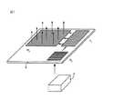
国際公開番号WO99/52002には、仮想表示装置の射出ひとみを拡大する方法が開示されている。この開示された方法では、3つの連続するホログラフィ光学素子(HOE)を用いて射出ひとみが拡大される。特に、HOEは図1に図示のような平らな光透過基板6上に配設された回析格子素子である。図示のように、画像ソース2から出た光は、基板6の1つの側部に設けた第1のHOEすなわちH1に対する入射光である。基板6の中へ結合されたH1から出た光は、第2のHOEすなわちH2へ向けられ、そこで配光は1つの方向に拡大される。H2もこの拡大された配光を第3のHOEすなわちH3へ再指向させ、そこで、上記配光は別の方向にさらに拡大される。ホログラフィエレメントは基板6のいずれの側に在るものであってもよい。H3も、H3が配置されている基板面から外へ向かってこの拡大された配光の再指向を行う。光学系は、図1に図示のように、光ビームの一般的方向を維持するビーム光拡大用素子として作動する。このような素子は射出ひとみエクステンダ(exit pupil extender:EPE)と呼ばれている。 International Publication No. WO99 / 52002 discloses a method for enlarging an exit pupil of a virtual display device. In the disclosed method, the exit pupil is enlarged using three consecutive holographic optical elements (HOE). In particular, the HOE is a diffraction grating element disposed on a flat
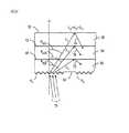
図1に図示のようなEPEは結果として色むらを生み、そのため再現されるバーチャル画像の品質の低下をもたらすことになる。色むらは異なる色の光ビームが、図2に図示のように基板6内の異なる経路を進むという事実に起因して生じるものである。例示を目的として、λ1とλ2とによって表す2色のみを用いて、従来技術のEPEにおける色むらのソースを示すことにする(ここで、λ1<λ2)。The EPE as shown in FIG. 1 results in color shading and thus a reduction in the quality of the reproduced virtual image. Color shading is caused by the fact that light beams of different colors follow different paths in the
図2では、2つのHOEしか用いられていないが、色むらのソースは3つまたはそれ以上のHOEを使用する場合でも同じである。第1のHOEすなわちH1は、一般に、基板6の中へ入射光を結合し、次いで、基板6内の配光を第2のHOEすなわちH2の方へ向ける、平行な回析縞から成る回析構造を有する。基板は、主として総内反射(TIR)によって基板の2つの表面間で光ビームを捕捉する光導波路として機能する。図2に図示のように、回折素子H1とH2の双方が基板6の下面に設けられる。このような光デバイスでは、TIRは上面側のみで完了する。というのは、光の一部が基板の下面から視る人の目へ向かって外側へ回折されるからである。 In FIG. 2, only two HOEs are used, but the source of color shading is the same when using three or more HOEs. The first HOE or H1 generally couples incident light into the
基板6の内部の回折角が下式によって決定されることが知られている。
sin(θi)−n sin(θm)=m λ/d (1)
ここで、
dは回折素子(この場合H1)の格子周期、
λは波長、
nは基板の屈折率、
mは回折次数、
θiは入射角、そして、
θmはm番目の次数における回折角である。
数式1からわかるように、回折角θmは波長λと共に増加する。したがって、回折角θm1は回折角θm2よりも小さくなる。この結果、2つの連続するTIR間の間隔Lも波長と共に変動する。λ1の間隔L1はλ2の間隔L2よりも狭くなる。したがって、η方向の送出配光はすべての波長について均一ではなくなる(図6を参照のこと)。ここで、出力信号が1つの波長(青など。図6を参照のこと)について均質となるように格子構造を設計することは可能である。図2でわかるように、短い方の波長λ1が、回折素子H2上でλ2よりも多くの“ヒット”を経験する。その結果、短い方の波長λ1の多くの光がH1の近くの領域内の回折素子H2の中から“漏出する”。3原色(赤、緑、青)が用いる表示装置では、図2のEPEに起因してムラのある光の色分布が生じる。これによって、H1に対して相対的に、近端部では色が青っぽく現れ、遠端部では色が赤っぽく現れる場合がある。η方向に沿って距離が増すにつれて、むらのある色分布はさらに顕著になる。It is known that the diffraction angle inside the
sin (θi ) −n sin (θm ) = m λ / d (1)
here,
d is the grating period of the diffractive element (in this case H1),
λ is wavelength,
n is the refractive index of the substrate,
m is the diffraction order,
θi is the angle of incidence, and
θm is the diffraction angle at the m-th order.
As can be seen from Equation 1, the diffraction angle θm increases with the wavelength λ. Therefore, the diffraction angle θm1 is smaller than the diffraction angle θm2 . As a result, the distance L between two successive TIRs also varies with wavelength. lambda1 of the distance L1 becomes smaller than the interval L2 of lambda2. Therefore, the light distribution in the η direction is not uniform for all wavelengths (see FIG. 6). Here, it is possible to design the grating structure so that the output signal is uniform with respect to one wavelength (such as blue, see FIG. 6). As can be seen in FIG. 2, the shorter wavelength λ1 experiences more “hits” on diffractive element H2 than λ2 . As a result, much light of the shorter wavelength λ1 “leaks” out of the diffractive element H 2 in the region near H 1. In the display device using the three primary colors (red, green, and blue), uneven color distribution of light occurs due to the EPE in FIG. As a result, the color may appear bluish at the near end and the color may appear red at the far end relative to H1. The uneven color distribution becomes more pronounced as the distance increases along the η direction.
H2が配置されている基板6の下面から、あるいは、上面から光が“漏出する”可能性があることに留意されたい。上面からの送出配光は下面からの送出配光の場合と同様である。 Note that light can "leak" from the bottom surface of the
射出ひとみエクステンダ内での配光時における色の均一性を改良する方法およびシステムを提供することが好都合であり、望ましい。 It would be advantageous and desirable to provide a method and system that improves color uniformity during light distribution within an exit pupil extender.
異なる波長に対する連続する総内反射間の間隔の差を小さくするか、この差を取り除くことが本発明の主要な目的である。この目的の達成は、複数の層を設けた基板を用いて、1つの色の総内反射が異なる層表面で生じるようにすることにより可能となる。 It is a major object of the present invention to reduce or eliminate the difference in spacing between successive total internal reflections for different wavelengths. This object can be achieved by using a substrate having a plurality of layers so that total internal reflection of one color occurs on different layer surfaces.
したがって、本発明の第1の形態によれば、光デバイスが提供され、上記光デバイスは、
第1の面および対向する第2の面を有するほぼ平らな光導波部材と、
上記光導波用部材の中へ光波を結合するための、上記光導波用部材に対して相対的に配置した光結合手段であって、上記第1の面と第2の面との間で上記光波が進むにつれて、上記光導波用部材が、連続する内部反射に実質的に基づいて上記光導波用部材内で上記光波を導き、さらに、上記光波が、少なくとも第1の色の第1の光波と、第2の異なる色の第2の光波とを含む光結合手段と、を具備し、さらに前記光デバイスは、上記第1の反射角で上記第1の光波を内部反射し、上記第1の面または第2の面の垂直な面に関して上記第1の反射角よりも大きな第2の反射角で上記第2の光波を内部反射し、
上記第2の面から上記第1の面へ向かって上記第2の光波が進むにつれて、上記境界面を通して上記第1の光波を透過することを可能にしながら、上記第2の面へ向かって上記第2の光波を反射するように、上記第1の面と上記第2の面との間に設けられた少なくとも1つのほぼ平らな境界面を具備することを特徴とする。Therefore, according to the first aspect of the present invention, an optical device is provided, the optical device comprising:
A substantially flat optical waveguide member having a first surface and an opposing second surface;
An optical coupling means disposed relative to the optical waveguide member for coupling light waves into the optical waveguide member, wherein the optical coupling means is disposed between the first surface and the second surface. As the light wave travels, the light guide member guides the light wave within the light guide member substantially based on continuous internal reflection, and the light wave further includes a first light wave of at least a first color. And an optical coupling means including a second light wave of a second different color, and the optical device internally reflects the first light wave at the first reflection angle, The second light wave is internally reflected at a second reflection angle that is greater than the first reflection angle with respect to a plane perpendicular to the second surface or the second surface;
As the second light wave travels from the second surface toward the first surface, the first light wave can be transmitted through the boundary surface, while moving toward the second surface. It is characterized by comprising at least one substantially flat boundary surface provided between the first surface and the second surface so as to reflect the second light wave.
上記第2の面における上記第1の光波による上記連続する内部反射が、第1の反射間隔によって分離された複数の第1の反射点において生じ、上記第2の面における上記第2の光波による上記連続する内部反射が、第2の反射間隔によって分離された複数の第2の反射点において生じる光デバイスは、
上記第1の面と第2の面との間に上記境界面を配置して、上記第1の反射間隔と上記第2の反射間隔間の差を小さくするか、上記差を取り除くようにすることをさらに特徴とする。The continuous internal reflection due to the first light wave at the second surface occurs at a plurality of first reflection points separated by a first reflection interval, and due to the second light wave at the second surface. An optical device in which the continuous internal reflection occurs at a plurality of second reflection points separated by a second reflection interval is:
The boundary surface is disposed between the first surface and the second surface so as to reduce or eliminate the difference between the first reflection interval and the second reflection interval. This is further characterized.
好適には、上記第2の面を通して上記光導波用部材の中へ上記光波を結合するように上記光結合手段を配置することが望ましい。 Preferably, the optical coupling means is arranged so as to couple the light wave through the second surface and into the optical waveguide member.
好適には、上記第2の面の一部に出会う上記光波を上記第2の面を通して部分的に透過させるために、光結合手段を上記光導波用部材に対して相対的に配置することが望ましい。 Preferably, in order to partially transmit the light wave that meets a part of the second surface through the second surface, optical coupling means may be disposed relative to the optical waveguide member. desirable.
或いは、上記第2の面の一部に出会う上記光波を上記第2の面を通して部分的に透過させるために、さらなる光結合手段を上記光導波用部材に対して相対的に配置して、
上記境界面を通して、次いで上記第1の面を通して上記第2の面の一部に出会う上記光波の一部を透過させ、
上記反射角を保持しながら、上記第2の面から上記第1の面へ向かって上記第2の面の一部に出会う上記光波の別の部分を反射させるようにすることが望ましい。Alternatively, in order to partially transmit the light wave that meets a part of the second surface through the second surface, further optical coupling means is disposed relative to the optical waveguide member,
Transmitting a portion of the light wave that meets a portion of the second surface through the interface and then through the first surface;
It is desirable to reflect another portion of the light wave that meets a portion of the second surface from the second surface toward the first surface while maintaining the reflection angle.
好適には、上記光結合手段が回折素子を具備することが望ましい。 Preferably, the optical coupling means includes a diffractive element.
好適には、上記光結合手段と上記さらなる光結合手段とは上記光導波用部材上に設けたホログラフ回折素子であることが望ましい。 Preferably, the optical coupling means and the further optical coupling means are holographic diffraction elements provided on the optical waveguide member.
好適には、上記光波は上記第1および第2の色とは異なる第3の色の第3の光波をさらに含み、上記第1および上記第2の反射角よりも小さな第3の反射角で上記第3の光波を内部反射する光デバイスにおいて、
上記第1の面と上記境界面との間にさらなる境界面を設けて、上記さらなる境界面を通して上記第3の光波を透過できるようにしながら、上記第2の面から上記第1の面へ向かって上記第1の光波が進むにつれて、上記第2の面へ向かって上記第1の光波を反射するようにすることが望ましい。Preferably, the light wave further includes a third light wave of a third color different from the first and second colors, and at a third reflection angle smaller than the first and second reflection angles. In the optical device for internally reflecting the third light wave,
A further boundary surface is provided between the first surface and the boundary surface so that the third light wave can be transmitted through the further boundary surface, and from the second surface to the first surface. It is desirable that the first light wave is reflected toward the second surface as the first light wave travels.
上記光導波用部材が第1の屈折率を有する光学材料からつくられた光デバイスにおいて、
上記境界面が上記第1の屈折率よりも小さな第2の屈折率を有する光学材料からつくられた層であって、それによって、上記境界面における上記第2の光波による反射が総内反射となるようにする。In the optical device in which the optical waveguide member is made of an optical material having a first refractive index,
The boundary surface is a layer made of an optical material having a second refractive index smaller than the first refractive index, whereby reflection by the second light wave at the boundary surface is total internal reflection. To be.
上記さらなる境界面が、上記第1の屈折率よりも小さな第2の屈折率を有する光学材料からつくられた層であり、それによって、さらなる境界面における上記第1の光波による反射が総内反射となるようにする。 The further interface is a layer made of an optical material having a second refractive index less than the first refractive index, whereby reflection by the first light wave at the further interface is total internal reflection. To be.
本発明の第2の形態によれば、光デバイスにおける色の均一性を改善する方法が提供され、上記光デバイスは、
第1の面および対向する第2の面を有するほぼ平らな光導波部材と、
光導波用部材の中へ光波を結合するための、上記光導波用部材に対して相対的に配置した光結合手段であって、上記第1の面と第2の面との間で上記光波が進むにつれて、上記光導波用部材が、連続する内部反射に実質的に基づいて上記光導波用部材内で上記光波を導き、さらに、上記光波が、少なくとも第1の色の第1の光波と、第2の異なる色の第2の光波とを含む光結合手段と、を具備し、第1の反射角で上記第1の光波を内部反射し、上記第1の面または第2の面の垂直な面に関して上記第1の反射角よりも大きな第2の反射角で上記第2の光波を内部反射する方法において、
上記第1の面と上記第2の面との間に少なくとも1つのほぼ平らな境界面を設けて、上記第2の面から上記第1の面へ向かって上記第2の光波が進むにつれて、上記境界面を通して上記第1の光波を透過させることを可能にしながら、上記第2の面へ向かって上記第2の光波を反射させるようにする。According to a second aspect of the present invention, there is provided a method for improving color uniformity in an optical device, the optical device comprising:
A substantially flat optical waveguide member having a first surface and an opposing second surface;
An optical coupling means disposed relative to the optical waveguide member for coupling an optical wave into the optical waveguide member, the optical wave between the first surface and the second surface. As the light wave travels, the light guide member guides the light wave within the light guide member substantially based on successive internal reflections, and the light wave further comprises at least a first light wave of a first color. And an optical coupling means including a second light wave of a second different color, and internally reflects the first light wave at a first reflection angle, the first surface or the second surface In a method of internally reflecting the second light wave at a second reflection angle greater than the first reflection angle with respect to a vertical plane,
As the second light wave travels from the second surface toward the first surface by providing at least one substantially flat boundary surface between the first surface and the second surface, The second light wave is reflected toward the second surface while allowing the first light wave to pass through the boundary surface.
好適には、上記第2の面における上記第1の光波による上記連続する内部反射が、第1の反射間隔によって分離された複数の第1の反射点において生じ、
上記第2の面における上記第2の光波による上記連続する内部反射が、第2の反射間隔によって分離された複数の第2の反射点において生じ、
上記第1の面と第2の面との間に上記境界面を配置して、上記第1の反射間隔と上記第2の反射間隔間の差を小さくするか、上記差を取り除くステップをさらに特徴とすることが望ましい。Preferably, the continuous internal reflection by the first light wave on the second surface occurs at a plurality of first reflection points separated by a first reflection interval,
The continuous internal reflection by the second light wave on the second surface occurs at a plurality of second reflection points separated by a second reflection interval;
Disposing the boundary surface between the first surface and the second surface to reduce or eliminate the difference between the first reflection interval and the second reflection interval; It is desirable to have a feature.
上記方法は、上記第2の面を通して上記光導波用部材の中へ上記光波を結合することをさらに特徴とする。 The method is further characterized in that the light wave is coupled into the optical waveguide member through the second surface.
本発明の第3の形態によれば、以下の、
ハウジングと、
閲覧可能情報を示す光波を出力するために上記ハウジング内に設けた画像ソースと、
視る人が上記光デバイスを介して上記閲覧可能情報を閲覧できるようにするために、上記光波を受け取るように上記画像ソースと作動してリンクされた光デバイスと、を具備する電子デバイスが提供され、上記光デバイスは、
第1の面および対向する第2の面を有するほぼ平らな光導波部材と、
光導波用部材の中へ光波を結合するための、上記光導波用部材に対して相対的に配置した光結合手段であって、上記第1の面と第2の面との間で上記光波が進むにつれて、上記光導波用部材が、連続する内部反射に実質的に基づいて上記光導波用部材内で上記光波を導き、さらに、上記光波が、少なくとも第1の色の第1の光波と、第2の異なる色の第2の光波とを含む光結合手段と、を具備し、第1の反射角で上記第1の光波を内部反射し、上記第1の面または第2の面の垂直な面に関して上記第1の反射角よりも大きな第2の反射角で上記第2の光波を内部反射する電子デバイスにおいて、
上記光デバイスが、上記第1の面と上記第2の面との間に少なくとも1つのほぼ平らな境界面を設けて、上記第2の面から上記第1の面へ向かって上記第2の光波が進むにつれて、上記境界面を通して上記第1の光波を透過させることを可能にしながら、上記第2の面へ向かって上記第2の光波を反射させるようにすることを特徴とする。According to the third aspect of the present invention,
A housing;
An image source provided in the housing for outputting light waves indicating viewable information;
An electronic device comprising: an optical device operatively linked with the image source to receive the light wave to allow a viewer to view the viewable information via the optical device And the optical device is
A substantially flat optical waveguide member having a first surface and an opposing second surface;
An optical coupling means disposed relative to the optical waveguide member for coupling an optical wave into the optical waveguide member, the optical wave between the first surface and the second surface. As the light wave travels, the light guide member guides the light wave within the light guide member substantially based on successive internal reflections, and the light wave further comprises at least a first light wave of a first color. And an optical coupling means including a second light wave of a second different color, and internally reflects the first light wave at a first reflection angle, the first surface or the second surface In an electronic device that internally reflects the second light wave at a second reflection angle that is greater than the first reflection angle with respect to a vertical plane,
The optical device includes at least one substantially flat boundary surface between the first surface and the second surface, and the second device from the second surface toward the first surface. As the light wave advances, the second light wave is reflected toward the second surface while allowing the first light wave to pass through the boundary surface.
好適には、上記第2の面の一部に出会う上記光波を上記第2の面を通して部分的に透過させて、視る人が上記第2の面の上記部分を通して上記閲覧可能情報を閲覧できるようにするために、さらなる光結合手段を上記光導波用部材に対して相対的に配置することが望ましい。 Preferably, the light wave that meets a part of the second surface is partially transmitted through the second surface so that a viewer can view the viewable information through the portion of the second surface. In order to do so, it is desirable to dispose further optical coupling means relative to the optical waveguide member.
好適には、電子デバイスが、
上記受信信号を示すデータを上記画像ソースへ出力する外部ソースから上記閲覧可能情報を示す信号を受け取るための、上記画像ソースと作動してリンクされる通信手段をさらに特徴とすることが望ましい。Preferably, the electronic device is
It is desirable to further feature communication means operatively linked with the image source for receiving the signal indicative of the viewable information from an external source that outputs data indicative of the received signal to the image source.
上記電子デバイスは、移動端末装置、コミュニケータ装置、コンピュータ、等であってもよい。 The electronic device may be a mobile terminal device, a communicator device, a computer, or the like.
図3a〜図9と関連して行う説明を読むとき、本発明は明らかになる。 The present invention will become apparent when reading the description given in connection with FIGS.
図2に図示のような均質な基板6を使用する代わりに、本発明の射出ひとみエクステンダ(EPE)10は図3a〜3cに図示のような複数の層から成る基板60を使用する。 Instead of using a
図3aに図示のように、基板60は光学材料からなる第1の層30と、光学材料からなる第2の層50とを有し、短い方の波長λ1の総内反射(TIR)が空中/基板境界面32で生じるようになっているのに対して、長い方の波長λ2のTIRは第1の層30と第2の層50との間の境界面で生じるようになっている。好適には、第1の層30と第2の層50との間に薄膜40を設けることが望ましい。例えば、薄膜40は第2の層50の屈折率よりも低い屈折率を持つ材料からつくられる。第2の層50がガラスまたはプラスチックからつくられる場合、AlF3、NAF、氷晶石などから薄膜40をつくって、短い方の波長の光から赤色光(λ2)を分離することができる。これらの薄膜材料の屈折率は1.35のオーダーである。したがって、赤色光72が薄膜40と第2の層50との間の境界面で反射されるのに対して、短い方の波長74の光は薄膜40を透過することができる境界面32で反射させる。その場合、第1の層30と第2の層50は、異なる光学材料からつくられたものであってもよいし、あるいは、同じ光学材料からつくられたものであってもよい。個々の層の相対的厚さは、第1の回折素子H1における入射光70の所定の入射角度θiにおける異なる波長λ1とλ2とに対応する回折角θm1とθm2とによって決定される。基板60に対する表面垂線Nに関して、回折角θm1とθm2は基板60内の対応する波長の内反射角と同じである。As shown in FIG. 3a, the
図3aに図示のように、λ1の連続するTIR間の間隔L1と、λ2の間隔L2とは、層30、50の正確な厚さを選択することによりほぼ同じにすることができる。λ1の回折角θmをθ1、λ2の回折角θmをθ2とし、かつ、第1の層30の厚さがT1で、第2の層50の厚さをT2とすれば、(T1+T2)/T2=(tanθ2/tanθ1)となる。ここで、層30の屈折率は層50の屈折率と同じであると仮定する。したがって、短い方の波長λ1が経験する“ヒット”の数は、基板60の下面52に設けた回折素子H2上の長い方の波長λ2による“ヒット”の数とほぼ同じである。図示のように、光82(λ2)と光84(λ1)の出口点の数はほぼ同じである。したがって、第2の回折素子H2の中から回折される出力光80の色の均一性が改善される(図7〜図9を参照のこと)。しかし、同じ格子から出る短い方の波長と比べると、長い方の波長の回折効率は一般に低い。したがって、十分にバランスのとれたシステムでは間隔長は全く同じというわけではない。この場合、長い方の波長が短い方の波長よりも短い間隔長を有することになる。As shown in FIG. 3a, the spacing L1 between successive TIRs of λ1 and the spacing L2 of λ2 can be made approximately the same by selecting the exact thickness of the
図3aで、送出光80は、基板60の下面52の回折素子H2から直接現れる。同様に、図3bに図示のように短い方の波長λ1の光92と長い方の波長λ2の光94とを含む送出光90は基板60の上面32から現れることができる。この場合、回折素子H2は、反射光72、74を、薄膜40を通して上方へ回折させ、密/疎(dense-rare)境界面32を通して屈折させる。In FIG. 3 a, the transmitted
図3aと3bは、2つの層30、50のみを用いて2つの波長λ1とλ2用の反射面を設け、2つの波長の配光の改善を図るようにするEPEの概略図である。3つのまたはそれ以上の波長用のEPEに対して同じ原理を拡張することができる。図3cに図示のように、基板60は、反射用の3つの境界面を設けるために、光学材料からなる3つの層36、34、50を備える。例えば、入射光70が赤、緑、青の光から成る場合、3つの回折ビーム光72(赤)、76(緑)74(青)が基板60内で捕捉される。その場合、青色光用のTIRは空中/基板境界面32で生じ、緑色光用のTIRは層34と36との間の境界面で生じ、赤色光用のTIRは層34と50との間の境界面で生じる。3a and 3b are schematic diagrams of an EPE that uses only two
好適には、層34と層50との間に薄膜40を設け、層34と層36との間に薄膜42を設けることが望ましい。緑色光と青色光とから赤色光を分離するために、薄膜40はAlF3、NAF、あるいは氷晶石であってもよい。しかし、青色光から緑色光を分離するために薄膜42はさらに低い屈折率を有することが望ましい。1.2のオーダーの屈折率を持つ薄膜材料が米国特許第5,882,773号明細書(Chow他)に開示されている。個々の層の正しい相対的厚さを用いることにより、赤色光の反射間の間隔L1は、緑色光用の間隔L2並びに青色光用の間隔L3にほぼ等しくすることが可能である。Preferably, the
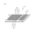
本発明によれば、EPE10は、H2が1つの方向に配光を拡大するように相互に隣接して配設された2つの回折素子H1、H2を備える。回折素子H1とH2との例示構成が図4に図示されている。移動電話、個人用情報機器(PDA)、コミュニケータ、携帯用インターネット機器、ハンドヘルド型コンピュータ、デジタルビデオおよびスチルカメラ、着用可能コンピュータ、コンピュータゲーム装置、閲覧用の特殊な接眼式(bring-to-the-eye)製品、その他の携帯用電子装置などの携帯用デバイス100でEPE10を使用することができる。図5に図示のように、携帯用デバイス100は、外部装置(図示せず)から、並びに、外部装置(図示せず)へ情報の送受信を行う通信ユニット112を収納するハウジング110を備える。携帯用デバイス100は、送受信済み情報を処理する制御および処理ユニット114、並びに、閲覧用の仮想表示システム130も備える。仮想表示システム130は、マイクロ表示装置すなわち画像ソース132および光学エンジン134を備える。制御および処理ユニット114は光学エンジン134と作動して接続され、画像を表示する画像ソース132へ画像データの出力を行う。本発明によれば、EPE10は光学エンジン134と光学的にリンクすることができる。 In accordance with the present invention, the
本発明に基づくEPEにおける選択反射制御の原理を例示するために、双眼式表示装置に関するシミュレーション研究が行われてきた。図6〜図9に図示のプロットは、3つの波長:赤、緑、青に対応する距離ηの関数としての強度分布を表わす。縦軸の単位は光子の数であり、横軸の単位はmmである。青色波長が表示領域全体にわたって均質になるように格子深度が選択される。 In order to illustrate the principle of selective reflection control in EPE according to the present invention, simulation studies on binocular display devices have been conducted. The plots shown in FIGS. 6-9 represent intensity distributions as a function of distance η corresponding to three wavelengths: red, green and blue. The unit of the vertical axis is the number of photons, and the unit of the horizontal axis is mm. The grating depth is selected so that the blue wavelength is uniform throughout the display area.
図6では、基板は、図2の基板6と類似した光学材料からなる平板にすぎない。ここで、図2の基板6には色を分離する薄膜は使用されない。3色間での反射間隔Lの差に起因して、赤色は表示領域にわたって均質ではない。 In FIG. 6, the substrate is only a flat plate made of an optical material similar to the
図3aと3bに図示のように、緑色光と青色光から赤色光を分離するために1つの薄膜が基板の中へ組み込まれている場合、表示領域にわたって赤色光を均質にすることができる。しかし、緑色光の反射間隔は変更されないため、緑色の出力光の分布は図7に図示のように表示領域にわたって均質ではない。1つの薄膜を利用して緑色と赤色とを青色から分離する場合、表示領域にわたって緑色が均質になるが、これに対して、図8に図示のように赤色は均質にはならない。 As shown in FIGS. 3a and 3b, if a thin film is incorporated into the substrate to separate red light from green and blue light, the red light can be homogenized across the display area. However, since the green light reflection interval is not changed, the distribution of the green output light is not uniform over the display area as shown in FIG. When green and red are separated from blue using one thin film, green is uniform over the display area, whereas red is not uniform as shown in FIG.
図3cに例示の薄膜と同様の2つの薄膜を利用して赤色と緑色の反射間隔を別々に変更する場合、3色のすべてが図9に図示のように表示領域にわたって均質になる。図3cでは、薄膜40は緑色と青色から赤色を分離し、薄膜42が青色から緑色をさらに分離する。 If two thin films similar to the thin film illustrated in FIG. 3c are utilized to change the red and green reflection spacings separately, all three colors are homogeneous across the display area as illustrated in FIG. In FIG. 3c,
回折素子H1とH2の各々をホログラフ回折素子(HOE)あるいは回析光学素子(DOE)とすることも可能であることに留意されたい。この名称が示唆するように、ホログラフィ回折素子はホログラフィを用いて形成される素子であり、この素子で少なくとも2つのコヒーレントな光ビームを利用して干渉縞が生みだされる。これとは対照的に、回折光学素子は機械的にまたは化学的に形成することができる。EPE10は2または3以上の回折素子であってもよい。 Note that each of the diffractive elements H1 and H2 can be a holographic diffractive element (HOE) or a diffractive optical element (DOE). As the name suggests, a holographic diffractive element is an element formed using holography, in which interference fringes are produced using at least two coherent light beams. In contrast, diffractive optical elements can be formed mechanically or chemically. The
本発明の目的は異なる波長間でほぼ均一な反射間隔(L1、L2、L3)を達成することであり、したがって、長い方の波長の光を選択的に反射するために、薄膜40または42の代わりに、マルチ層コーティングを利用することも可能となる。さらに、本発明のEPEの適用は仮想表示装置に限定されるものではない。本発明に基づいて、1または2以上の方向の光学的ビーム光の拡大が必要となり、かつ、異なる波長の光が使用されるアプリケーションで平板導波路(基板60)での選択反射制御を利用することが可能である。回折素子(H1、H2)は、実際には、平板導波路内へ光を結合するための光カプラおよび光変調装置である。したがって、EPE10は、図3a〜3cに図示のように、光の結合と操作を行う目的のために、導波路に隣接して、あるいは、導波路上に設けた平板導波路と複数の光カプラ(または光変調装置)とから構成された光デバイスと見なすことができ、光カプラのうちの1または2以上は回折素子または非回折素子であってもよい。 The object of the present invention is to achieve a substantially uniform reflection spacing (L1, L2, L3) between different wavelengths, and thus to selectively reflect the longer wavelength light, Alternatively, a multi-layer coating can be used. Furthermore, the application of the EPE of the present invention is not limited to a virtual display device. In accordance with the present invention, selective reflection control in a planar waveguide (substrate 60) is utilized in applications where optical beam light in one or more directions is required and light of different wavelengths is used. It is possible. The diffractive elements (H1, H2) are actually optical couplers and light modulators for coupling light into the planar waveguide. Thus, as shown in FIGS. 3a-3c, the
図5に描かれているように、画像ソース132は、シーケンシャルなカラーLCOS(シリコン上液晶)装置、OLED(有機発光ダイオード)アレイ、MEMS(マイクロ電気機械的システム)装置においてあるいは送信、反射または放射時に作動する他の任意の好適なマイクロ表示装置であってもよい。 As depicted in FIG. 5, the image source 132 may be a sequential color LCOS (Liquid Crystal on Silicon) device, an OLED (Organic Light Emitting Diode) array, a MEMS (Micro Electro Mechanical System) device, or transmit, reflect or emit. It may be any other suitable micro display device that sometimes operates.
したがって、本発明の好ましい実施形態と関連して本発明について説明したが、本発明の範囲から逸脱することなく、細部を形成する際に本発明の上述の変更、省略、逸脱およびその他の種々の変更、省略、逸脱を行うことができる。 Thus, although the invention has been described in connection with a preferred embodiment of the invention, the above-described modifications, omissions, departures and various other modifications of the invention may be made in forming details without departing from the scope of the invention. Changes, omissions and deviations can be made.
10 射出ひとみエクステンダ(EPE)
30 第1の層
32 空中/基板境界面
34,36 層
40 薄膜
50 第2の層
52 基板の下面
60 基板
70 入射光
72 赤色光(反射光:赤)
74 短い方の波長(反射光:青)
76 反射光(緑)
80 出力光
90 送出光
92 短い方の波長の光
94 長い方の波長の光
100 携帯用デバイス
110 ハウジング
112 通信ユニット
114 処理ユニット
130 仮想表示システム
132 マイクロ表示装置(画像ソース)
134 光学エンジン10 Injection pupil extender (EPE)
30
74 Shorter wavelength (reflected light: blue)
76 Reflected light (green)
80
134 Optical engine
Claims (22)
Translated fromJapanese前記光導波用部材の中へ光波を結合するための、前記光導波用部材に対して相対的に配置した光結合手段であって、前記第1の面と第2の面との間で前記光波が進むにつれて、前記光導波用部材が、連続する内部反射に実質的に基づいて前記光導波用部材内で前記光波を導き、さらに、前記光波が、少なくとも第1の色の第1の光波と、第2の異なる色の第2の光波とを具備する光結合手段と、を具備する光デバイスにおいて、第1の反射角で前記第1の光波を内部反射し、前記第1の面または第2の面の垂直面に関して前記第1の反射角よりも大きな第2の反射角で前記第2の光波を内部反射し、
前記第2の面から前記第1の面へ向かって前記第2の光波が進むにつれて、境界面を通して前記第1の光波を透過できるようにしながら、前記第2の面へ向かって前記第2の光波を反射するように、前記第1の面と前記第2の面との間に設けられた少なくとも1つのほぼ平らな前記境界面を具備することを特徴とする光デバイス。A substantially flat optical waveguide member having a first surface and an opposing second surface;
An optical coupling means disposed relative to the optical waveguide member for coupling an optical wave into the optical waveguide member, wherein the optical coupling means is disposed between the first surface and the second surface; As the light wave travels, the light guiding member guides the light wave within the light guiding member substantially based on continuous internal reflection, and the light wave further comprises a first light wave of at least a first color. And an optical coupling means comprising a second light wave of a second different color, and internally reflecting the first light wave at a first reflection angle, Internally reflecting the second light wave at a second reflection angle greater than the first reflection angle with respect to a vertical plane of the second surface;
As the second light wave travels from the second surface toward the first surface, the second light wave transmits toward the second surface while allowing the first light wave to pass through the boundary surface. An optical device comprising at least one substantially flat boundary surface provided between the first surface and the second surface so as to reflect a light wave.
前記第2の面における前記第1の光波による前記連続する内部反射が、第1の反射間隔によって分離された複数の第1の反射点において生じ、
前記第2の面における前記第2の光波による前記連続する内部反射が、第2の反射間隔によって分離された複数の第2の反射点において生じる光デバイスにおいて、
前記第1の面と第2の面との間に前記境界面を配置して、前記第1の反射間隔と前記第2の反射間隔間の差を小さくするか、上記差を取り除くようにすることをさらに特徴とする光デバイス。The optical device according to claim 1.
The continuous internal reflection by the first light wave on the second surface occurs at a plurality of first reflection points separated by a first reflection interval;
In the optical device in which the continuous internal reflection by the second light wave on the second surface occurs at a plurality of second reflection points separated by a second reflection interval,
The boundary surface is disposed between the first surface and the second surface to reduce or eliminate the difference between the first reflection interval and the second reflection interval. An optical device characterized by that.
前記第2の面を通して前記光導波用部材の中へ前記光波を結合するように前記光結合手段を配置することを特徴とする光デバイス。The optical device according to claim 1 or 2,
An optical device comprising: the optical coupling means arranged to couple the light wave through the second surface and into the optical waveguide member.
前記第2の面の一部に出会う前記光波を前記第2の面を通して部分的に透過させるために、光結合手段を前記光導波用部材に対して相対的に配置することをさらなる特徴とする光デバイス。The optical device according to any one of claims 1 to 3,
Further characterized in that an optical coupling means is disposed relative to the optical waveguide member in order to partially transmit the light wave that encounters a part of the second surface through the second surface. Optical device.
前記光導波用部材に対して相対的に配置したさらなる光結合手段であって、
前記境界面を通して、次いで前記第1の面を通して前記第2の面の一部に出会う前記光波の一部を透過させ、
前記反射角を保持しながら、前記第2の面から前記第1の面へ向かって前記第2の面の一部に出会う前記光波の別の部分を反射させるようにする光結合手段をさらに特徴とする光デバイス。The optical device according to any one of claims 1 to 3,
A further optical coupling means arranged relative to the optical waveguide member,
Transmitting a portion of the light wave that encounters a portion of the second surface through the interface and then through the first surface;
Optical coupling means for reflecting another portion of the light wave that meets a portion of the second surface from the second surface toward the first surface while maintaining the reflection angle is further characterized. And optical device.
前記第1の面と前記境界面との間にさらなる境界面を設け、前記さらなる境界面を通して前記第3の光波を透過できるようにしながら、前記第2の面から前記第1の面へ向かって前記第1の光波が進むにつれて、前記第2の面へ向かって前記第1の光波を反射するようにすることをさらに特徴とする光デバイス。9. The optical device according to claim 1, wherein the light wave further includes a third light wave having a third color different from the first and second colors. The third light wave is internally reflected at a third reflection angle smaller than the reflection angle of 2,
A further boundary surface is provided between the first surface and the boundary surface, and the third light wave can be transmitted through the further boundary surface, and from the second surface toward the first surface. The optical device is further characterized by reflecting the first light wave toward the second surface as the first light wave travels.
前記境界面が、前記第1の屈折率よりも小さな第2の屈折率を有する光学材料からつくられた層であって、それによって、前記境界面における前記第2の光波による反射が総内反射となるようにすることをさらに特徴とする光デバイス。The optical device according to claim 1, wherein the optical waveguide member is made of an optical material having a first refractive index,
The boundary surface is a layer made of an optical material having a second refractive index smaller than the first refractive index, whereby reflection by the second light wave at the boundary surface is total internal reflection. An optical device further characterized by:
前記さらなる境界面が、前記第1の屈折率よりも小さな第2の屈折率を有する光学材料からつくられた層であり、それによって、さらなる境界面における前記第1の光波による反射が総内反射となるようにすることをさらに特徴とする光デバイス。The optical device according to claim 9, wherein the optical waveguide member is an optical material having a first refractive index.
The further interface is a layer made of an optical material having a second refractive index less than the first refractive index, whereby reflection by the first light wave at the further interface is total internal reflection. An optical device further characterized by:
第1の面および対向する第2の面を有するほぼ平らな光導波部材と、
光導波用部材の中へ光波を結合するための、前記光導波用部材に対して相対的に配置した光結合手段であって、前記第1の面と第2の面との間で前記光波が進むにつれて、前記光導波用部材が、連続する内部反射に実質的に基づいて前記光導波用部材内で前記光波を導き、さらに、前記光波が、少なくとも第1の色の第1の光波と、第2の異なる色の第2の光波とを含む光結合手段と、を具備し、第1の反射角で前記第1の光波を内部反射し、前記第1の面または第2の面の垂直な面に関して前記第1の反射角よりも大きな第2の反射角で前記第2の光波を内部反射する方法において、
前記第1の面と前記第2の面との間に少なくとも1つのほぼ平らな境界面を設けて、前記第2の面から前記第1の面へ向かって前記第2の光波が進むにつれて、前記境界面を通して前記第1の光波を透過できるようにしながら、前記第2の面へ向かって前記第2の光波を反射させるようにすることを特徴とする方法。A method for improving color uniformity in an optical device, the optical device comprising:
A substantially flat optical waveguide member having a first surface and an opposing second surface;
An optical coupling means disposed relative to the optical waveguide member for coupling an optical wave into the optical waveguide member, the optical wave between the first surface and the second surface. As the light wave travels, the light guide member guides the light wave within the light guide member substantially based on continuous internal reflection, and the light wave further comprises a first light wave of at least a first color. An optical coupling means including a second light wave of a second different color, and internally reflecting the first light wave at a first reflection angle, wherein the first surface or the second surface In a method of internally reflecting the second light wave with a second reflection angle that is greater than the first reflection angle with respect to a vertical plane,
Providing at least one substantially flat interface between the first surface and the second surface, and as the second light wave travels from the second surface toward the first surface, A method of reflecting the second light wave toward the second surface while allowing the first light wave to pass through the boundary surface.
前記第2の面における前記第1の光波による前記連続する内部反射が、第1の反射間隔によって分離された複数の第1の反射点において生じ、
前記第2の面における前記第2の光波による前記連続する内部反射が、第2の反射間隔によって分離された複数の第2の反射点において生じ、
前記第1の面と第2の面との間に前記境界面を配置して、前記第1の反射間隔と前記第2の反射間隔との差を小さくするか、上記差を取り除くステップをさらに特徴とする方法。The method of claim 12, wherein
The continuous internal reflection by the first light wave on the second surface occurs at a plurality of first reflection points separated by a first reflection interval;
The continuous internal reflection by the second light wave on the second surface occurs at a plurality of second reflection points separated by a second reflection interval;
Disposing the boundary surface between the first surface and the second surface to further reduce or eliminate the difference between the first reflection interval and the second reflection interval; Feature method.
前記第2の面を通して前記光導波用部材の中へ前記光波を結合することをさらに特徴とする方法。The method according to claim 12 or 13, wherein:
The method further comprises coupling the light wave through the second surface into the optical waveguide member.
閲覧可能情報を示す光波を出力するために前記ハウジング内に設けた画像ソースと、
視る人が前記光デバイスを介して前記閲覧可能情報を閲覧できるようにするために、前記光波を受け取るように前記画像ソースと作動してリンクされた光デバイスと、を具備する電子デバイスにおいて、前記光デバイスが、
第1の面および対向する第2の面を有するほぼ平らな光導波部材と、
光導波用部材の中へ光波を結合するための、前記光導波用部材に対して相対的に配置した光結合手段であって、前記第1の面と第2の面との間で前記光波が進むにつれて、前記光導波用部材が、連続する内部反射に実質的に基づいて前記光導波用部材内で前記光波を導き、さらに、前記光波が、少なくとも第1の色の第1の光波と、第2の異なる色の第2の光波とを含む光結合手段と、を具備し、第1の反射角で前記第1の光波を内部反射し、前記第1の面または第2の面の垂直な面に関して前記第1の反射角よりも大きな第2の反射角で前記第2の光波を内部反射する電子デバイスにおいて、
前記光デバイスが、前記第1の面と前記第2の面との間に少なくとも1つのほぼ平らな境界面を設けて、前記第2の面から前記第1の面へ向かって前記第2の光波が進むにつれて、前記境界面を通して前記第1の光波を透過できるようにしながら、前記第2の面へ向かって前記第2の光波を反射させるようにすることを特徴とする電子デバイス。A housing;
An image source provided in the housing for outputting light waves indicating viewable information;
In an electronic device comprising: an optical device operatively linked with the image source to receive the light wave to enable a viewer to view the viewable information via the optical device; The optical device is
A substantially flat optical waveguide member having a first surface and an opposing second surface;
An optical coupling means disposed relative to the optical waveguide member for coupling an optical wave into the optical waveguide member, the optical wave between the first surface and the second surface. As the light wave travels, the light guide member guides the light wave within the light guide member substantially based on continuous internal reflection, and the light wave further comprises a first light wave of at least a first color. An optical coupling means including a second light wave of a second different color, and internally reflecting the first light wave at a first reflection angle, wherein the first surface or the second surface In an electronic device that internally reflects the second light wave at a second reflection angle that is greater than the first reflection angle with respect to a vertical plane,
The optical device includes at least one substantially flat boundary surface between the first surface and the second surface, and the second device from the second surface toward the first surface. As the light wave travels, the second light wave is reflected toward the second surface while allowing the first light wave to be transmitted through the boundary surface.
前記第2の面における前記第1の光波による前記連続する内部反射が、第1の反射間隔によって分離された複数の第1の反射点において生じ、
前記第2の面における前記第2の光波による前記連続する内部反射が、第2の反射間隔によって分離された複数の第2の反射点において生じ、
前記第1の面と第2の面との間に前記境界面を配置して、前記第1の反射間隔と前記第2の反射間隔との差を小さくするか、上記差を取り除くようにすることをさらに特徴とする電子デバイス。The electronic device according to claim 15.
The continuous internal reflection by the first light wave on the second surface occurs at a plurality of first reflection points separated by a first reflection interval;
The continuous internal reflection by the second light wave on the second surface occurs at a plurality of second reflection points separated by a second reflection interval;
The boundary surface is disposed between the first surface and the second surface to reduce or eliminate the difference between the first reflection interval and the second reflection interval. An electronic device characterized by that.
前記第2の面の一部に出会う前記光波を前記第2の面を通して部分的に透過させて、視る人が前記第2の面の一部を通して前記閲覧可能情報を閲覧できるようにするために前記光導波用部材に対して相対的に配置したさらなる光結合手段をさらに特徴とする電子デバイス。The electronic device according to claim 15 or 16,
In order to allow the viewer to view the viewable information through a part of the second surface by partially transmitting the light wave that meets a part of the second surface through the second surface. An electronic device further comprising further optical coupling means disposed relative to the optical waveguide member.
前記境界面を通して、次いで前記第1の面を通して前記第2の面の一部に出会う前記光波の一部を透過させ、
前記反射角を保持しながら、前記第2の面から前記第1の面へ向かって前記第2の面の一部に出会う前記光波の別の部分を反射させるための、前記光導波用部材に対して相対的に配置したさらなる光結合手段をさらに特徴とする電子デバイス。The electronic device according to claim 15 or 16,
Transmitting a portion of the light wave that encounters a portion of the second surface through the interface and then through the first surface;
The optical waveguide member for reflecting another part of the light wave that meets a part of the second surface from the second surface toward the first surface while maintaining the reflection angle. An electronic device further characterized by further optical coupling means arranged relative to the device.
前記受信信号を示すデータを前記画像ソースへ出力する外部ソースから、前記閲覧可能情報を示す信号を受け取るための、前記画像ソースと作動してリンクされた通信手段をさらに特徴とする電子デバイス。The electronic device according to any one of claims 15 to 18,
An electronic device further comprising communication means operatively linked with the image source for receiving a signal indicative of the viewable information from an external source that outputs data indicative of the received signal to the image source.
Applications Claiming Priority (2)
| Application Number | Priority Date | Filing Date | Title |
|---|---|---|---|
| US10/261,236US6805490B2 (en) | 2002-09-30 | 2002-09-30 | Method and system for beam expansion in a display device |
| US10/261,236 | 2002-09-30 |
Related Parent Applications (1)
| Application Number | Title | Priority Date | Filing Date |
|---|---|---|---|
| JP2004539363ADivisionJP2006501499A (en) | 2002-09-30 | 2003-09-29 | Beam light expanding method and system in display device |
Publications (2)
| Publication Number | Publication Date |
|---|---|
| JP2008112187Atrue JP2008112187A (en) | 2008-05-15 |
| JP5175086B2 JP5175086B2 (en) | 2013-04-03 |
Family
ID=32029915
Family Applications (2)
| Application Number | Title | Priority Date | Filing Date |
|---|---|---|---|
| JP2004539363AWithdrawnJP2006501499A (en) | 2002-09-30 | 2003-09-29 | Beam light expanding method and system in display device |
| JP2007340491AExpired - LifetimeJP5175086B2 (en) | 2002-09-30 | 2007-12-28 | Beam light expanding method and system in display device |
Family Applications Before (1)
| Application Number | Title | Priority Date | Filing Date |
|---|---|---|---|
| JP2004539363AWithdrawnJP2006501499A (en) | 2002-09-30 | 2003-09-29 | Beam light expanding method and system in display device |
Country Status (6)
| Country | Link |
|---|---|
| US (1) | US6805490B2 (en) |
| EP (1) | EP1546816A2 (en) |
| JP (2) | JP2006501499A (en) |
| CN (1) | CN100470272C (en) |
| AU (1) | AU2003267703A1 (en) |
| WO (1) | WO2004030160A2 (en) |
Cited By (51)
| Publication number | Priority date | Publication date | Assignee | Title |
|---|---|---|---|---|
| JP2016085426A (en)* | 2014-10-29 | 2016-05-19 | セイコーエプソン株式会社 | Optical element, electro-optic device, mount-type display device, and optical element manufacturing method |
| US10089516B2 (en) | 2013-07-31 | 2018-10-02 | Digilens, Inc. | Method and apparatus for contact image sensing |
| US10145533B2 (en) | 2005-11-11 | 2018-12-04 | Digilens, Inc. | Compact holographic illumination device |
| US10156681B2 (en) | 2015-02-12 | 2018-12-18 | Digilens Inc. | Waveguide grating device |
| US10185154B2 (en) | 2011-04-07 | 2019-01-22 | Digilens, Inc. | Laser despeckler based on angular diversity |
| US10209517B2 (en) | 2013-05-20 | 2019-02-19 | Digilens, Inc. | Holographic waveguide eye tracker |
| US10216061B2 (en) | 2012-01-06 | 2019-02-26 | Digilens, Inc. | Contact image sensor using switchable bragg gratings |
| US10234696B2 (en) | 2007-07-26 | 2019-03-19 | Digilens, Inc. | Optical apparatus for recording a holographic device and method of recording |
| US10241330B2 (en) | 2014-09-19 | 2019-03-26 | Digilens, Inc. | Method and apparatus for generating input images for holographic waveguide displays |
| US10330777B2 (en) | 2015-01-20 | 2019-06-25 | Digilens Inc. | Holographic waveguide lidar |
| US10359736B2 (en) | 2014-08-08 | 2019-07-23 | Digilens Inc. | Method for holographic mastering and replication |
| US10423222B2 (en) | 2014-09-26 | 2019-09-24 | Digilens Inc. | Holographic waveguide optical tracker |
| US10437051B2 (en) | 2012-05-11 | 2019-10-08 | Digilens Inc. | Apparatus for eye tracking |
| US10437064B2 (en) | 2015-01-12 | 2019-10-08 | Digilens Inc. | Environmentally isolated waveguide display |
| US10459145B2 (en) | 2015-03-16 | 2019-10-29 | Digilens Inc. | Waveguide device incorporating a light pipe |
| US10545346B2 (en) | 2017-01-05 | 2020-01-28 | Digilens Inc. | Wearable heads up displays |
| US10591756B2 (en) | 2015-03-31 | 2020-03-17 | Digilens Inc. | Method and apparatus for contact image sensing |
| US10642058B2 (en) | 2011-08-24 | 2020-05-05 | Digilens Inc. | Wearable data display |
| CN111226157A (en)* | 2017-10-13 | 2020-06-02 | 康宁股份有限公司 | Waveguide-based optical system and method for augmented reality system |
| US10670876B2 (en) | 2011-08-24 | 2020-06-02 | Digilens Inc. | Waveguide laser illuminator incorporating a despeckler |
| US10678053B2 (en) | 2009-04-27 | 2020-06-09 | Digilens Inc. | Diffractive projection apparatus |
| US10690851B2 (en) | 2018-03-16 | 2020-06-23 | Digilens Inc. | Holographic waveguides incorporating birefringence control and methods for their fabrication |
| US10690916B2 (en) | 2015-10-05 | 2020-06-23 | Digilens Inc. | Apparatus for providing waveguide displays with two-dimensional pupil expansion |
| US10732569B2 (en) | 2018-01-08 | 2020-08-04 | Digilens Inc. | Systems and methods for high-throughput recording of holographic gratings in waveguide cells |
| US10890707B2 (en) | 2016-04-11 | 2021-01-12 | Digilens Inc. | Holographic waveguide apparatus for structured light projection |
| US10914950B2 (en) | 2018-01-08 | 2021-02-09 | Digilens Inc. | Waveguide architectures and related methods of manufacturing |
| US10942430B2 (en) | 2017-10-16 | 2021-03-09 | Digilens Inc. | Systems and methods for multiplying the image resolution of a pixelated display |
| US10983340B2 (en) | 2016-02-04 | 2021-04-20 | Digilens Inc. | Holographic waveguide optical tracker |
| US11204540B2 (en) | 2009-10-09 | 2021-12-21 | Digilens Inc. | Diffractive waveguide providing a retinal image |
| JP2022510841A (en)* | 2018-11-22 | 2022-01-28 | ロベルト・ボッシュ・ゲゼルシャフト・ミト・ベシュレンクテル・ハフツング | Optical coupling device for projecting images |
| US11307432B2 (en) | 2014-08-08 | 2022-04-19 | Digilens Inc. | Waveguide laser illuminator incorporating a Despeckler |
| US11378732B2 (en) | 2019-03-12 | 2022-07-05 | DigLens Inc. | Holographic waveguide backlight and related methods of manufacturing |
| US11402801B2 (en) | 2018-07-25 | 2022-08-02 | Digilens Inc. | Systems and methods for fabricating a multilayer optical structure |
| US11442222B2 (en) | 2019-08-29 | 2022-09-13 | Digilens Inc. | Evacuated gratings and methods of manufacturing |
| US11448937B2 (en) | 2012-11-16 | 2022-09-20 | Digilens Inc. | Transparent waveguide display for tiling a display having plural optical powers using overlapping and offset FOV tiles |
| US11460621B2 (en) | 2012-04-25 | 2022-10-04 | Rockwell Collins, Inc. | Holographic wide angle display |
| US11480788B2 (en) | 2015-01-12 | 2022-10-25 | Digilens Inc. | Light field displays incorporating holographic waveguides |
| US11513350B2 (en) | 2016-12-02 | 2022-11-29 | Digilens Inc. | Waveguide device with uniform output illumination |
| US11543594B2 (en) | 2019-02-15 | 2023-01-03 | Digilens Inc. | Methods and apparatuses for providing a holographic waveguide display using integrated gratings |
| US11604314B2 (en) | 2016-03-24 | 2023-03-14 | Digilens Inc. | Method and apparatus for providing a polarization selective holographic waveguide device |
| US11681143B2 (en) | 2019-07-29 | 2023-06-20 | Digilens Inc. | Methods and apparatus for multiplying the image resolution and field-of-view of a pixelated display |
| US11726332B2 (en) | 2009-04-27 | 2023-08-15 | Digilens Inc. | Diffractive projection apparatus |
| US11747568B2 (en) | 2019-06-07 | 2023-09-05 | Digilens Inc. | Waveguides incorporating transmissive and reflective gratings and related methods of manufacturing |
| US12092914B2 (en) | 2018-01-08 | 2024-09-17 | Digilens Inc. | Systems and methods for manufacturing waveguide cells |
| US12140764B2 (en) | 2019-02-15 | 2024-11-12 | Digilens Inc. | Wide angle waveguide display |
| US12158612B2 (en) | 2021-03-05 | 2024-12-03 | Digilens Inc. | Evacuated periodic structures and methods of manufacturing |
| US12210153B2 (en) | 2019-01-14 | 2025-01-28 | Digilens Inc. | Holographic waveguide display with light control layer |
| US12222499B2 (en) | 2020-12-21 | 2025-02-11 | Digilens Inc. | Eye glow suppression in waveguide based displays |
| US12306585B2 (en) | 2018-01-08 | 2025-05-20 | Digilens Inc. | Methods for fabricating optical waveguides |
| US12397477B2 (en) | 2019-02-05 | 2025-08-26 | Digilens Inc. | Methods for compensating for optical surface nonuniformity |
| US12399326B2 (en) | 2021-01-07 | 2025-08-26 | Digilens Inc. | Grating structures for color waveguides |
Families Citing this family (135)
| Publication number | Priority date | Publication date | Assignee | Title |
|---|---|---|---|---|
| US8071740B2 (en)* | 2000-11-17 | 2011-12-06 | Vascular Biogenics Ltd. | Promoters exhibiting endothelial cell specificity and methods of using same for regulation of angiogenesis |
| US6838452B2 (en) | 2000-11-24 | 2005-01-04 | Vascular Biogenics Ltd. | Methods employing and compositions containing defined oxidized phospholipids for prevention and treatment of atherosclerosis |
| DE60237777D1 (en) | 2001-10-19 | 2010-11-04 | Vascular Biogenics Ltd | EFFECTS AND METHODS FOR THE TARGETED DOWN ALLGATION OF ANGIOGENESIS AND CANCER THERAPY |
| US6805490B2 (en)* | 2002-09-30 | 2004-10-19 | Nokia Corporation | Method and system for beam expansion in a display device |
| FI114946B (en)* | 2002-12-16 | 2005-01-31 | Nokia Corp | Diffractive grating element for balancing diffraction efficiency |
| US7205960B2 (en) | 2003-02-19 | 2007-04-17 | Mirage Innovations Ltd. | Chromatic planar optic display system |
| US7499216B2 (en)* | 2004-07-23 | 2009-03-03 | Mirage Innovations Ltd. | Wide field-of-view binocular device |
| US7492512B2 (en)* | 2004-07-23 | 2009-02-17 | Mirage International Ltd. | Wide field-of-view binocular device, system and kit |
| US7206107B2 (en)* | 2004-12-13 | 2007-04-17 | Nokia Corporation | Method and system for beam expansion in a display device |
| EP1828832B1 (en)* | 2004-12-13 | 2013-05-22 | Nokia Corporation | General diffractive optics method for expanding an exit pupil |
| FI20045513A7 (en)* | 2004-12-31 | 2006-07-01 | Nokia Corp | Pen-type virtual display |
| US7573640B2 (en)* | 2005-04-04 | 2009-08-11 | Mirage Innovations Ltd. | Multi-plane optical apparatus |
| JP4862298B2 (en)* | 2005-06-30 | 2012-01-25 | ソニー株式会社 | Optical device and virtual image display device |
| WO2007031992A1 (en)* | 2005-09-14 | 2007-03-22 | Mirage Innovations Ltd. | Diffraction grating with a spatially varying duty-cycle |
| US20080043334A1 (en)* | 2006-08-18 | 2008-02-21 | Mirage Innovations Ltd. | Diffractive optical relay and method for manufacturing the same |
| EP1943556B1 (en)* | 2005-11-03 | 2009-02-11 | Mirage Innovations Ltd. | Binocular optical relay device |
| WO2007085682A1 (en) | 2006-01-26 | 2007-08-02 | Nokia Corporation | Eye tracker device |
| CN105212890B (en)* | 2006-01-26 | 2017-04-26 | 诺基亚公司 | Eye tracker equipment |
| JP2007219106A (en)* | 2006-02-16 | 2007-08-30 | Konica Minolta Holdings Inc | Optical device for expanding diameter of luminous flux, video display device and head mount display |
| CN101460882B (en)* | 2006-06-02 | 2010-10-27 | 诺基亚公司 | Apparatus and method for providing color separation in exit pupil expander and electronic device |
| WO2007141588A1 (en)* | 2006-06-02 | 2007-12-13 | Nokia Corporation | Split exit pupil expander |
| EP2033040B1 (en)* | 2006-06-02 | 2020-04-29 | Magic Leap, Inc. | Stereoscopic exit pupil expander display |
| WO2008023375A1 (en)* | 2006-08-23 | 2008-02-28 | Mirage Innovations Ltd. | Diffractive optical relay device with improved color uniformity |
| WO2008038058A1 (en) | 2006-09-28 | 2008-04-03 | Nokia Corporation | Beam expansion with three-dimensional diffractive elements |
| WO2008059098A1 (en)* | 2006-11-16 | 2008-05-22 | Nanocomp Ltd | An arrangement and a method for coupling light into a plate-like light guide |
| US20080117635A1 (en)* | 2006-11-17 | 2008-05-22 | Ko-Ju Chen | Multi-Layer Light Guiding Structure And Method For Using The Same |
| US7455416B2 (en)* | 2006-11-17 | 2008-11-25 | Ichia Technologies, Inc. | Light guide structure and keypad having the same |
| US7423229B2 (en)* | 2006-11-17 | 2008-09-09 | Ichia Technologies, Inc. | Light guiding plate and a keystroke module for use therewith |
| US7650056B2 (en)* | 2006-11-17 | 2010-01-19 | Ichia Technologies, Inc. | Method for manufacturing a light-guiding plate and key module having the light-guiding plate |
| WO2008071830A1 (en)* | 2006-12-14 | 2008-06-19 | Nokia Corporation | Display device having two operating modes |
| US20100302644A1 (en)* | 2007-09-18 | 2010-12-02 | Mirage Innovations Ltd | Slanted optical device |
| JP4450058B2 (en)* | 2007-11-29 | 2010-04-14 | ソニー株式会社 | Image display device |
| WO2009077802A1 (en)* | 2007-12-18 | 2009-06-25 | Nokia Corporation | Exit pupil expanders with wide field-of-view |
| DE102008005817A1 (en) | 2008-01-24 | 2009-07-30 | Carl Zeiss Ag | Optical display device |
| US10795160B1 (en) | 2014-09-25 | 2020-10-06 | Rockwell Collins, Inc. | Systems for and methods of using fold gratings for dual axis expansion |
| US11320571B2 (en) | 2012-11-16 | 2022-05-03 | Rockwell Collins, Inc. | Transparent waveguide display providing upper and lower fields of view with uniform light extraction |
| US11300795B1 (en) | 2009-09-30 | 2022-04-12 | Digilens Inc. | Systems for and methods of using fold gratings coordinated with output couplers for dual axis expansion |
| US8233204B1 (en) | 2009-09-30 | 2012-07-31 | Rockwell Collins, Inc. | Optical displays |
| US20200057353A1 (en) | 2009-10-09 | 2020-02-20 | Digilens Inc. | Compact Edge Illuminated Diffractive Display |
| JP5059079B2 (en)* | 2009-10-21 | 2012-10-24 | キヤノン株式会社 | Laminated diffractive optical element and optical system |
| US8659826B1 (en) | 2010-02-04 | 2014-02-25 | Rockwell Collins, Inc. | Worn display system and method without requiring real time tracking for boresight precision |
| US8548290B2 (en)* | 2011-08-23 | 2013-10-01 | Vuzix Corporation | Dynamic apertured waveguide for near-eye display |
| EP3309602A1 (en)* | 2011-08-29 | 2018-04-18 | Vuzix Corporation | Controllable waveguide for near-eye display applications |
| US9507150B1 (en) | 2011-09-30 | 2016-11-29 | Rockwell Collins, Inc. | Head up display (HUD) using a bent waveguide assembly |
| US9366864B1 (en) | 2011-09-30 | 2016-06-14 | Rockwell Collins, Inc. | System for and method of displaying information without need for a combiner alignment detector |
| US9715067B1 (en) | 2011-09-30 | 2017-07-25 | Rockwell Collins, Inc. | Ultra-compact HUD utilizing waveguide pupil expander with surface relief gratings in high refractive index materials |
| US8634139B1 (en) | 2011-09-30 | 2014-01-21 | Rockwell Collins, Inc. | System for and method of catadioptric collimation in a compact head up display (HUD) |
| GB2500631B (en)* | 2012-03-27 | 2017-12-27 | Bae Systems Plc | Improvements in or relating to optical waveguides |
| US9523852B1 (en) | 2012-03-28 | 2016-12-20 | Rockwell Collins, Inc. | Micro collimator system and method for a head up display (HUD) |
| US8807817B2 (en)* | 2012-08-13 | 2014-08-19 | 3M Innovative Properties Company | Colorful diffractive luminaires providing white light illumination |
| US9674413B1 (en) | 2013-04-17 | 2017-06-06 | Rockwell Collins, Inc. | Vision system and method having improved performance and solar mitigation |
| US9244281B1 (en) | 2013-09-26 | 2016-01-26 | Rockwell Collins, Inc. | Display system and method using a detached combiner |
| EP3063570B1 (en)* | 2013-10-29 | 2021-03-17 | CSEM Centre Suisse D'electronique Et De Microtechnique SA | Optical grating coupling structure |
| KR102202454B1 (en)* | 2013-11-29 | 2021-01-14 | 엘지디스플레이 주식회사 | Thin Film Type Controlled Viewing Window Back Light Unit And Thin Flat Type Controlled Viewing Window Display Using The Same |
| FR3014209B1 (en)* | 2013-11-29 | 2017-03-03 | Commissariat Energie Atomique | OUTPUT PUPIL EXTENSION DEVICE AND HIGH HEAD VIEWER HAVING THE DEVICE |
| KR101731141B1 (en)* | 2013-12-31 | 2017-04-28 | 엘지디스플레이 주식회사 | Thin Film Type Back Light Unit For Flat Panel Display |
| US10732407B1 (en) | 2014-01-10 | 2020-08-04 | Rockwell Collins, Inc. | Near eye head up display system and method with fixed combiner |
| US9519089B1 (en) | 2014-01-30 | 2016-12-13 | Rockwell Collins, Inc. | High performance volume phase gratings |
| US9244280B1 (en) | 2014-03-25 | 2016-01-26 | Rockwell Collins, Inc. | Near eye display system and method for display enhancement or redundancy |
| US9529196B1 (en) | 2014-06-05 | 2016-12-27 | Iphysicist Ltd. | Image guide optics for near eye displays |
| RU2594370C2 (en) | 2014-07-11 | 2016-08-20 | Самсунг Электроникс Ко., Лтд. | Light-guide structure, optical device and imaging system |
| RU2603238C2 (en) | 2014-07-15 | 2016-11-27 | Самсунг Электроникс Ко., Лтд. | Light-guide structure, holographic optical device and imaging system |
| GB2529003B (en)* | 2014-08-03 | 2020-08-26 | Wave Optics Ltd | Optical device |
| US10088675B1 (en) | 2015-05-18 | 2018-10-02 | Rockwell Collins, Inc. | Turning light pipe for a pupil expansion system and method |
| US9715110B1 (en) | 2014-09-25 | 2017-07-25 | Rockwell Collins, Inc. | Automotive head up display (HUD) |
| CN112925100B (en) | 2014-09-29 | 2023-10-31 | 奇跃公司 | Optical system |
| IL237337B (en)* | 2015-02-19 | 2020-03-31 | Amitai Yaakov | Compact head-mounted display system having uniform image |
| CN104765085B (en)* | 2015-03-23 | 2017-10-13 | 美昇科技(成都)有限公司 | A kind of linear frequency domain grating and its design method |
| US11366316B2 (en) | 2015-05-18 | 2022-06-21 | Rockwell Collins, Inc. | Head up display (HUD) using a light pipe |
| US10247943B1 (en) | 2015-05-18 | 2019-04-02 | Rockwell Collins, Inc. | Head up display (HUD) using a light pipe |
| US10126552B2 (en) | 2015-05-18 | 2018-11-13 | Rockwell Collins, Inc. | Micro collimator system and method for a head up display (HUD) |
| US9904063B2 (en)* | 2015-06-15 | 2018-02-27 | Innerscene, Inc. | Collimating display and methods |
| US10108010B2 (en) | 2015-06-29 | 2018-10-23 | Rockwell Collins, Inc. | System for and method of integrating head up displays and head down displays |
| US10670862B2 (en) | 2015-07-02 | 2020-06-02 | Microsoft Technology Licensing, Llc | Diffractive optical elements with asymmetric profiles |
| KR102274749B1 (en)* | 2015-09-05 | 2021-07-08 | 레이아 인코포레이티드 | Multicolor grid-coupled backlighting |
| US10007117B2 (en)* | 2015-09-10 | 2018-06-26 | Vuzix Corporation | Imaging light guide with reflective turning array |
| US10429645B2 (en) | 2015-10-07 | 2019-10-01 | Microsoft Technology Licensing, Llc | Diffractive optical element with integrated in-coupling, exit pupil expansion, and out-coupling |
| US10241332B2 (en)* | 2015-10-08 | 2019-03-26 | Microsoft Technology Licensing, Llc | Reducing stray light transmission in near eye display using resonant grating filter |
| US10234686B2 (en) | 2015-11-16 | 2019-03-19 | Microsoft Technology Licensing, Llc | Rainbow removal in near-eye display using polarization-sensitive grating |
| US9671615B1 (en)* | 2015-12-01 | 2017-06-06 | Microsoft Technology Licensing, Llc | Extended field of view in near-eye display using wide-spectrum imager |
| US10598932B1 (en) | 2016-01-06 | 2020-03-24 | Rockwell Collins, Inc. | Head up display for integrating views of conformally mapped symbols and a fixed image source |
| CN118112800A (en)* | 2016-03-01 | 2024-05-31 | 奇跃公司 | Reflective switching device for inputting light of different wavelengths into a waveguide |
| US10317679B2 (en) | 2016-04-04 | 2019-06-11 | Akonia Holographics, Llc | Light homogenization |
| KR102006267B1 (en)* | 2016-06-30 | 2019-10-02 | 엘지디스플레이 주식회사 | Flat Panel Display Embedding Optical Imaging Sensor |
| KR102515292B1 (en)* | 2016-11-30 | 2023-03-29 | 엘지디스플레이 주식회사 | Thin Flat Type Optical Imaging Sensor And Flat Panel Display Embedding Optical Imaging Sensor |
| EP4152077A1 (en) | 2016-11-30 | 2023-03-22 | Magic Leap, Inc. | Method and system for high resolution digitized display |
| KR102440209B1 (en)* | 2016-12-08 | 2022-09-05 | 엘지디스플레이 주식회사 | Flat Panel Display Embedding Optical Imaging Sensor |
| CN108182873B (en) | 2016-12-08 | 2020-08-07 | 乐金显示有限公司 | Flat panel display having optical image sensor embedded therein |
| WO2018125574A1 (en) | 2016-12-31 | 2018-07-05 | Vuzix Corporation | Imaging light guide with expanded light distribution |
| CN106547146A (en)* | 2017-01-22 | 2017-03-29 | 京东方科技集团股份有限公司 | Dot structure and its manufacture method, array base palte and display device |
| US10295824B2 (en) | 2017-01-26 | 2019-05-21 | Rockwell Collins, Inc. | Head up display with an angled light pipe |
| WO2018152235A1 (en)* | 2017-02-14 | 2018-08-23 | Optecks, Llc | Optical display system for augmented reality and virtual reality |
| JP7095678B2 (en)* | 2017-03-03 | 2022-07-05 | 大日本印刷株式会社 | Light guide, anti-counterfeiting article |
| WO2018190007A1 (en)* | 2017-04-13 | 2018-10-18 | ソニー株式会社 | Image display device |
| WO2018201301A1 (en)* | 2017-05-02 | 2018-11-08 | 深圳市柔宇科技有限公司 | Holographic waveguide display system |
| KR102418802B1 (en)* | 2017-05-02 | 2022-07-11 | 엘지디스플레이 주식회사 | Display Device |
| EP3635456A4 (en) | 2017-06-13 | 2021-01-13 | Vuzix Corporation | IMAGE LIGHT GUIDE WITH OVERLAPPING GRIDS WITH EXTENDED LIGHT DISTRIBUTION |
| CN107229088B (en) | 2017-08-07 | 2020-11-03 | 京东方科技集团股份有限公司 | Optical microstructure, manufacturing method of optical microstructure layer, light guide assembly and display device |
| CN107422474B (en) | 2017-08-14 | 2020-12-01 | 京东方科技集团股份有限公司 | A beam expansion structure and optical display module |
| KR102409393B1 (en)* | 2017-08-14 | 2022-06-15 | 삼성전자주식회사 | Light guide plate, backlight unit, and holographic display device having the same |
| KR102477096B1 (en) | 2017-08-30 | 2022-12-13 | 삼성전자주식회사 | Backlight unit including input coupler, holographic display apparatus including the backlight unit, and method of manufacturing the input coupler |
| WO2019079014A1 (en) | 2017-10-16 | 2019-04-25 | Akonia Holographics Llc | Two-dimensional light homogenization |
| US10942355B2 (en)* | 2018-01-22 | 2021-03-09 | Facebook Technologies, Llc | Systems, devices, and methods for tiled multi-monochromatic displays |
| KR102525223B1 (en)* | 2018-02-05 | 2023-04-25 | 삼성디스플레이 주식회사 | Backlight unit and display apparatus including the same |
| FI129306B (en)* | 2018-04-19 | 2021-11-30 | Dispelix Oy | Diffractive exit pupil expander arrangement for display applications |
| CN108345062B (en)* | 2018-05-07 | 2024-08-27 | 太若科技(北京)有限公司 | Waveguide assembly and display device |
| US10545275B1 (en) | 2018-07-16 | 2020-01-28 | Shenzhen Guangjian Technology Co., Ltd. | Light projecting method and device |
| US10641942B2 (en) | 2018-07-16 | 2020-05-05 | Shenzhen Guangjian Technology Co., Ltd. | Light projecting method and device |
| US10690752B2 (en)* | 2018-07-16 | 2020-06-23 | Shenzhen Guangjian Technology Co., Ltd. | Light projecting method and device |
| JP7137273B2 (en)* | 2018-07-20 | 2022-09-14 | 株式会社日立製作所 | Video display device and video display system |
| US11103763B2 (en) | 2018-09-11 | 2021-08-31 | Real Shot Inc. | Basketball shooting game using smart glasses |
| US11141645B2 (en) | 2018-09-11 | 2021-10-12 | Real Shot Inc. | Athletic ball game using smart glasses |
| US11803056B2 (en)* | 2018-09-14 | 2023-10-31 | Apple Inc. | Waveguided display systems |
| US10690846B2 (en)* | 2018-10-24 | 2020-06-23 | Shenzhen Guangjian Technology Co., Ltd. | Light projecting method and device |
| KR102816729B1 (en) | 2019-01-15 | 2025-06-04 | 루머스 리미티드 | Method for fabricating symmetrical light guide optical elements |
| US10585194B1 (en) | 2019-01-15 | 2020-03-10 | Shenzhen Guangjian Technology Co., Ltd. | Switchable diffuser projection systems and methods |
| US11656458B2 (en) | 2019-01-23 | 2023-05-23 | Fusao Ishii | Optics of a display using an optical light guide |
| US11567263B2 (en) | 2019-04-19 | 2023-01-31 | Ase Sailing, Inc. | Optical targeting device |
| AU2020300121B2 (en) | 2019-07-04 | 2024-06-13 | Lumus Ltd. | Image waveguide with symmetric beam multiplication |
| CN110596807B (en)* | 2019-08-20 | 2021-11-19 | 奥比中光科技集团股份有限公司 | Waveguide structure, display device, and electronic apparatus |
| US12111479B2 (en) | 2019-09-16 | 2024-10-08 | Lumus Ltd. | Image display system with beam multiplication |
| KR102796865B1 (en)* | 2019-09-24 | 2025-04-16 | 삼성전자주식회사 | Backlight unit and holographic display apparatus including the same |
| US11054566B2 (en)* | 2019-10-25 | 2021-07-06 | Facebook Technologies, Llc | Display waveguide with a high-index layer |
| CN111045146B (en)* | 2019-11-08 | 2022-03-29 | 奥比中光科技集团股份有限公司 | Grating type optical waveguide and light propagation regulating method thereof |
| TWI884834B (en) | 2019-12-05 | 2025-05-21 | 以色列商魯姆斯有限公司 | Optical device and method of fabricating optical device |
| CN115176190B (en) | 2020-05-24 | 2024-07-09 | 鲁姆斯有限公司 | Composite light guide optical element |
| WO2022008378A1 (en)* | 2020-07-06 | 2022-01-13 | Interdigital Ce Patent Holdings, Sas | Reflective in-coupler design with high refractive index element using second diffraction order for near-eye displays |
| CN114815233B (en)* | 2021-01-18 | 2023-06-27 | 宁波舜宇光电信息有限公司 | Augmented reality display device |
| CN115373062A (en)* | 2021-05-17 | 2022-11-22 | 上海鲲游科技有限公司 | Diffractive optical waveguide device and method therefor |
| KR20240046489A (en) | 2021-08-23 | 2024-04-09 | 루머스 리미티드 | Method for manufacturing composite light guiding optical elements with embedded coupling-in reflector |
| EP4411456A4 (en)* | 2021-09-30 | 2025-01-08 | Panasonic Intellectual Property Management Co., Ltd. | Optical system and image display device |
| KR20230077518A (en)* | 2021-11-25 | 2023-06-01 | 삼성전자주식회사 | Waveguide optical device and near eye display apparatus |
| CN116859641A (en)* | 2023-08-02 | 2023-10-10 | 深圳市光舟半导体技术有限公司 | AR diffraction optical waveguide structure with high brightness uniformity and use method thereof |
| GB202318762D0 (en)* | 2023-12-08 | 2024-01-24 | Nokia Technologies Oy | Light guidinf apparatus |
| GB2638464A (en)* | 2024-02-23 | 2025-08-27 | Nokia Technologies Oy | Optical apparatus, modules and devices |
Citations (5)
| Publication number | Priority date | Publication date | Assignee | Title |
|---|---|---|---|---|
| US4946253A (en)* | 1989-10-16 | 1990-08-07 | Arizona Board Of Regents For And On Behalf Of The University Of Arizona | Reconfigurable substrate-mode holographic interconnect apparatus and method |
| JPH0488312A (en)* | 1990-08-01 | 1992-03-23 | Fujitsu Ltd | Video superimposition device |
| JPH08122548A (en)* | 1994-10-18 | 1996-05-17 | Asahi Glass Co Ltd | Optical transmission device and optical transmission method |
| JP2002014213A (en)* | 2000-06-30 | 2002-01-18 | Minolta Co Ltd | Blaze grating device, diffraction grating device and illumination optical system |
| JP2006501499A (en)* | 2002-09-30 | 2006-01-12 | ノキア コーポレイション | Beam light expanding method and system in display device |
Family Cites Families (27)
| Publication number | Priority date | Publication date | Assignee | Title |
|---|---|---|---|---|
| DE3000402A1 (en)* | 1979-01-19 | 1980-07-31 | Smiths Industries Ltd | DISPLAY DEVICE |
| US4711512A (en)* | 1985-07-12 | 1987-12-08 | Environmental Research Institute Of Michigan | Compact head-up display |
| US4838630A (en) | 1987-12-21 | 1989-06-13 | Physical Optics Corporation | Holographic planar optical interconnect |
| US5880888A (en)* | 1989-01-23 | 1999-03-09 | Hughes Aircraft Company | Helmet mounted display system |
| JP3130329B2 (en) | 1991-05-31 | 2001-01-31 | セイコーインスツルメンツ株式会社 | Optical pattern recognition device |
| US5224198A (en) | 1991-09-30 | 1993-06-29 | Motorola, Inc. | Waveguide virtual image display |
| US5369415A (en)* | 1992-06-29 | 1994-11-29 | Motorola, Inc. | Direct retinal scan display with planar imager |
| DE69432526T2 (en)* | 1993-02-26 | 2004-04-01 | Yeda Research And Development Co., Ltd. | OPTICAL HOLOGRAPHIC DEVICES |
| JP3739821B2 (en) | 1993-10-04 | 2006-01-25 | モトローラ・インコーポレイテッド | Transceiver with small virtual image display |
| US5882773A (en)* | 1993-10-13 | 1999-03-16 | The Regents Of The University Of California | Optical coatings of variable refractive index and high laser-resistance from physical-vapor-deposited perfluorinated amorphous polymer |
| WO1996035288A1 (en) | 1995-05-03 | 1996-11-07 | Siemens Aktiengesellschaft | Portable radio communication device with inbtegrated camera and image display device |
| US6360104B1 (en)* | 1995-09-21 | 2002-03-19 | International Business Machines Corporation | Personal communicator including a handset phone with an integrated virtual image display |
| US5970418A (en) | 1995-09-21 | 1999-10-19 | International Business Machines Corporation | Personal communicator including a handset phone with an integrated virtual image display |
| US5867795A (en)* | 1996-08-23 | 1999-02-02 | Motorola, Inc. | Portable electronic device with transceiver and visual image display |
| US6486862B1 (en)* | 1996-10-31 | 2002-11-26 | Kopin Corporation | Card reader display system |
| US6577411B1 (en) | 1996-11-12 | 2003-06-10 | Planop-Planar Optics Ltd. | Optical system for alternative or simultaneous direction of light originating from two scenes to the eye of a viewer |
| US5724163A (en)* | 1996-11-12 | 1998-03-03 | Yariv Ben-Yehuda | Optical system for alternative or simultaneous direction of light originating from two scenes to the eye of a viewer |
| FI111892B (en)* | 1997-04-22 | 2003-09-30 | Nokia Oy Ab | Multifunctional communication device |
| IL121067A0 (en)* | 1997-06-12 | 1997-11-20 | Yeda Res & Dev | Compact planar optical correlator |
| US6275714B1 (en) | 1998-02-26 | 2001-08-14 | Inviso, Inc. | Phone with ergonomic virtual image display |
| EP1068548B1 (en) | 1998-04-02 | 2003-11-12 | Elop Electro-Optics Industries Ltd. | Holographic optical devices |
| US6334063B1 (en)* | 1998-12-17 | 2001-12-25 | Motorola, Inc. | Electronic device with auto-positioning virtual image display and associated method |
| US20030063042A1 (en) | 1999-07-29 | 2003-04-03 | Asher A. Friesem | Electronic utility devices incorporating a compact virtual image display |
| WO2001053917A2 (en)* | 2000-01-24 | 2001-07-26 | Sanjay Chadha | Hand-held personal computing device with microdisplay |
| US6999071B2 (en) | 2000-05-19 | 2006-02-14 | Tibor Balogh | Method and apparatus for displaying 3d images |
| ATE473464T1 (en) | 2000-06-05 | 2010-07-15 | Lumus Ltd | OPTICAL BEAM EXPANDER WITH SUBSTRATE LIGHT WAVE GUIDE |
| US7119843B2 (en)* | 2000-11-10 | 2006-10-10 | Sanyo Electric Co., Ltd. | Mobile phone provided with video camera |
- 2002
- 2002-09-30USUS10/261,236patent/US6805490B2/ennot_activeExpired - Lifetime
- 2003
- 2003-09-29EPEP03748396Apatent/EP1546816A2/ennot_activeWithdrawn
- 2003-09-29AUAU2003267703Apatent/AU2003267703A1/ennot_activeAbandoned
- 2003-09-29JPJP2004539363Apatent/JP2006501499A/ennot_activeWithdrawn
- 2003-09-29CNCNB038233096Apatent/CN100470272C/ennot_activeExpired - Lifetime
- 2003-09-29WOPCT/IB2003/004261patent/WO2004030160A2/ennot_activeApplication Discontinuation
- 2007
- 2007-12-28JPJP2007340491Apatent/JP5175086B2/ennot_activeExpired - Lifetime
Patent Citations (5)
| Publication number | Priority date | Publication date | Assignee | Title |
|---|---|---|---|---|
| US4946253A (en)* | 1989-10-16 | 1990-08-07 | Arizona Board Of Regents For And On Behalf Of The University Of Arizona | Reconfigurable substrate-mode holographic interconnect apparatus and method |
| JPH0488312A (en)* | 1990-08-01 | 1992-03-23 | Fujitsu Ltd | Video superimposition device |
| JPH08122548A (en)* | 1994-10-18 | 1996-05-17 | Asahi Glass Co Ltd | Optical transmission device and optical transmission method |
| JP2002014213A (en)* | 2000-06-30 | 2002-01-18 | Minolta Co Ltd | Blaze grating device, diffraction grating device and illumination optical system |
| JP2006501499A (en)* | 2002-09-30 | 2006-01-12 | ノキア コーポレイション | Beam light expanding method and system in display device |
Cited By (88)
| Publication number | Priority date | Publication date | Assignee | Title |
|---|---|---|---|---|
| US10145533B2 (en) | 2005-11-11 | 2018-12-04 | Digilens, Inc. | Compact holographic illumination device |
| US10234696B2 (en) | 2007-07-26 | 2019-03-19 | Digilens, Inc. | Optical apparatus for recording a holographic device and method of recording |
| US10725312B2 (en) | 2007-07-26 | 2020-07-28 | Digilens Inc. | Laser illumination device |
| US11175512B2 (en) | 2009-04-27 | 2021-11-16 | Digilens Inc. | Diffractive projection apparatus |
| US11726332B2 (en) | 2009-04-27 | 2023-08-15 | Digilens Inc. | Diffractive projection apparatus |
| US10678053B2 (en) | 2009-04-27 | 2020-06-09 | Digilens Inc. | Diffractive projection apparatus |
| US11204540B2 (en) | 2009-10-09 | 2021-12-21 | Digilens Inc. | Diffractive waveguide providing a retinal image |
| US11487131B2 (en) | 2011-04-07 | 2022-11-01 | Digilens Inc. | Laser despeckler based on angular diversity |
| US10185154B2 (en) | 2011-04-07 | 2019-01-22 | Digilens, Inc. | Laser despeckler based on angular diversity |
| US10670876B2 (en) | 2011-08-24 | 2020-06-02 | Digilens Inc. | Waveguide laser illuminator incorporating a despeckler |
| US11287666B2 (en) | 2011-08-24 | 2022-03-29 | Digilens, Inc. | Wearable data display |
| US11874477B2 (en) | 2011-08-24 | 2024-01-16 | Digilens Inc. | Wearable data display |
| US12306418B2 (en) | 2011-08-24 | 2025-05-20 | Rockwell Collins, Inc. | Wearable data display |
| US10642058B2 (en) | 2011-08-24 | 2020-05-05 | Digilens Inc. | Wearable data display |
| US10459311B2 (en) | 2012-01-06 | 2019-10-29 | Digilens Inc. | Contact image sensor using switchable Bragg gratings |
| US10216061B2 (en) | 2012-01-06 | 2019-02-26 | Digilens, Inc. | Contact image sensor using switchable bragg gratings |
| US11460621B2 (en) | 2012-04-25 | 2022-10-04 | Rockwell Collins, Inc. | Holographic wide angle display |
| US11994674B2 (en) | 2012-05-11 | 2024-05-28 | Digilens Inc. | Apparatus for eye tracking |
| US10437051B2 (en) | 2012-05-11 | 2019-10-08 | Digilens Inc. | Apparatus for eye tracking |
| US11448937B2 (en) | 2012-11-16 | 2022-09-20 | Digilens Inc. | Transparent waveguide display for tiling a display having plural optical powers using overlapping and offset FOV tiles |
| US12405507B2 (en) | 2012-11-16 | 2025-09-02 | Digilens Inc. | Transparent waveguide display with grating lamina that both couple and extract modulated light |
| US10209517B2 (en) | 2013-05-20 | 2019-02-19 | Digilens, Inc. | Holographic waveguide eye tracker |
| US11662590B2 (en) | 2013-05-20 | 2023-05-30 | Digilens Inc. | Holographic waveguide eye tracker |
| US10423813B2 (en) | 2013-07-31 | 2019-09-24 | Digilens Inc. | Method and apparatus for contact image sensing |
| US10089516B2 (en) | 2013-07-31 | 2018-10-02 | Digilens, Inc. | Method and apparatus for contact image sensing |
| US10359736B2 (en) | 2014-08-08 | 2019-07-23 | Digilens Inc. | Method for holographic mastering and replication |
| US11709373B2 (en) | 2014-08-08 | 2023-07-25 | Digilens Inc. | Waveguide laser illuminator incorporating a despeckler |
| US11307432B2 (en) | 2014-08-08 | 2022-04-19 | Digilens Inc. | Waveguide laser illuminator incorporating a Despeckler |
| US10241330B2 (en) | 2014-09-19 | 2019-03-26 | Digilens, Inc. | Method and apparatus for generating input images for holographic waveguide displays |
| US11726323B2 (en) | 2014-09-19 | 2023-08-15 | Digilens Inc. | Method and apparatus for generating input images for holographic waveguide displays |
| US10423222B2 (en) | 2014-09-26 | 2019-09-24 | Digilens Inc. | Holographic waveguide optical tracker |
| JP2016085426A (en)* | 2014-10-29 | 2016-05-19 | セイコーエプソン株式会社 | Optical element, electro-optic device, mount-type display device, and optical element manufacturing method |
| US10437064B2 (en) | 2015-01-12 | 2019-10-08 | Digilens Inc. | Environmentally isolated waveguide display |
| US11740472B2 (en) | 2015-01-12 | 2023-08-29 | Digilens Inc. | Environmentally isolated waveguide display |
| US11480788B2 (en) | 2015-01-12 | 2022-10-25 | Digilens Inc. | Light field displays incorporating holographic waveguides |
| US11726329B2 (en) | 2015-01-12 | 2023-08-15 | Digilens Inc. | Environmentally isolated waveguide display |
| US10330777B2 (en) | 2015-01-20 | 2019-06-25 | Digilens Inc. | Holographic waveguide lidar |
| US10156681B2 (en) | 2015-02-12 | 2018-12-18 | Digilens Inc. | Waveguide grating device |
| US12379547B2 (en) | 2015-02-12 | 2025-08-05 | Digilens Inc. | Waveguide grating device |
| US11703645B2 (en) | 2015-02-12 | 2023-07-18 | Digilens Inc. | Waveguide grating device |
| US10527797B2 (en) | 2015-02-12 | 2020-01-07 | Digilens Inc. | Waveguide grating device |
| US10459145B2 (en) | 2015-03-16 | 2019-10-29 | Digilens Inc. | Waveguide device incorporating a light pipe |
| US12013561B2 (en) | 2015-03-16 | 2024-06-18 | Digilens Inc. | Waveguide device incorporating a light pipe |
| US11169314B2 (en) | 2015-03-16 | 2021-11-09 | Digilens Inc. | Waveguide device incorporating a light pipe |
| US10591756B2 (en) | 2015-03-31 | 2020-03-17 | Digilens Inc. | Method and apparatus for contact image sensing |
| US11754842B2 (en) | 2015-10-05 | 2023-09-12 | Digilens Inc. | Apparatus for providing waveguide displays with two-dimensional pupil expansion |
| US12405471B2 (en) | 2015-10-05 | 2025-09-02 | Digilens Inc. | Apparatus for providing waveguide displays with two-dimensional pupil expansion |
| US10690916B2 (en) | 2015-10-05 | 2020-06-23 | Digilens Inc. | Apparatus for providing waveguide displays with two-dimensional pupil expansion |
| US11281013B2 (en) | 2015-10-05 | 2022-03-22 | Digilens Inc. | Apparatus for providing waveguide displays with two-dimensional pupil expansion |
| US10983340B2 (en) | 2016-02-04 | 2021-04-20 | Digilens Inc. | Holographic waveguide optical tracker |
| US11604314B2 (en) | 2016-03-24 | 2023-03-14 | Digilens Inc. | Method and apparatus for providing a polarization selective holographic waveguide device |
| US10890707B2 (en) | 2016-04-11 | 2021-01-12 | Digilens Inc. | Holographic waveguide apparatus for structured light projection |
| US12298513B2 (en) | 2016-12-02 | 2025-05-13 | Digilens Inc. | Waveguide device with uniform output illumination |
| US11513350B2 (en) | 2016-12-02 | 2022-11-29 | Digilens Inc. | Waveguide device with uniform output illumination |
| US12248150B2 (en) | 2017-01-05 | 2025-03-11 | Digilens Inc. | Wearable heads up displays |
| US10545346B2 (en) | 2017-01-05 | 2020-01-28 | Digilens Inc. | Wearable heads up displays |
| US11194162B2 (en) | 2017-01-05 | 2021-12-07 | Digilens Inc. | Wearable heads up displays |
| US11586046B2 (en) | 2017-01-05 | 2023-02-21 | Digilens Inc. | Wearable heads up displays |
| CN111226157A (en)* | 2017-10-13 | 2020-06-02 | 康宁股份有限公司 | Waveguide-based optical system and method for augmented reality system |
| CN111226157B (en)* | 2017-10-13 | 2022-06-17 | 康宁股份有限公司 | Waveguide-based optical system and method for augmented reality system |
| US10942430B2 (en) | 2017-10-16 | 2021-03-09 | Digilens Inc. | Systems and methods for multiplying the image resolution of a pixelated display |
| US10732569B2 (en) | 2018-01-08 | 2020-08-04 | Digilens Inc. | Systems and methods for high-throughput recording of holographic gratings in waveguide cells |
| US12366823B2 (en) | 2018-01-08 | 2025-07-22 | Digilens Inc. | Systems and methods for high-throughput recording of holographic gratings in waveguide cells |
| US12352960B2 (en) | 2018-01-08 | 2025-07-08 | Digilens Inc. | Waveguide architectures and related methods of manufacturing |
| US12306585B2 (en) | 2018-01-08 | 2025-05-20 | Digilens Inc. | Methods for fabricating optical waveguides |
| US10914950B2 (en) | 2018-01-08 | 2021-02-09 | Digilens Inc. | Waveguide architectures and related methods of manufacturing |
| US12092914B2 (en) | 2018-01-08 | 2024-09-17 | Digilens Inc. | Systems and methods for manufacturing waveguide cells |
| US10690851B2 (en) | 2018-03-16 | 2020-06-23 | Digilens Inc. | Holographic waveguides incorporating birefringence control and methods for their fabrication |
| US11726261B2 (en) | 2018-03-16 | 2023-08-15 | Digilens Inc. | Holographic waveguides incorporating birefringence control and methods for their fabrication |
| US11150408B2 (en) | 2018-03-16 | 2021-10-19 | Digilens Inc. | Holographic waveguides incorporating birefringence control and methods for their fabrication |
| US11402801B2 (en) | 2018-07-25 | 2022-08-02 | Digilens Inc. | Systems and methods for fabricating a multilayer optical structure |
| JP2022510841A (en)* | 2018-11-22 | 2022-01-28 | ロベルト・ボッシュ・ゲゼルシャフト・ミト・ベシュレンクテル・ハフツング | Optical coupling device for projecting images |
| JP7183418B2 (en) | 2018-11-22 | 2022-12-05 | ロベルト・ボッシュ・ゲゼルシャフト・ミト・ベシュレンクテル・ハフツング | optical coupler for projecting images |
| US12124030B2 (en) | 2018-11-22 | 2024-10-22 | Robert Bosch Gmbh | Optical combination device for projecting an image |
| US12210153B2 (en) | 2019-01-14 | 2025-01-28 | Digilens Inc. | Holographic waveguide display with light control layer |
| US12397477B2 (en) | 2019-02-05 | 2025-08-26 | Digilens Inc. | Methods for compensating for optical surface nonuniformity |
| US12140764B2 (en) | 2019-02-15 | 2024-11-12 | Digilens Inc. | Wide angle waveguide display |
| US11543594B2 (en) | 2019-02-15 | 2023-01-03 | Digilens Inc. | Methods and apparatuses for providing a holographic waveguide display using integrated gratings |
| US11378732B2 (en) | 2019-03-12 | 2022-07-05 | DigLens Inc. | Holographic waveguide backlight and related methods of manufacturing |
| US12271035B2 (en) | 2019-06-07 | 2025-04-08 | Digilens Inc. | Waveguides incorporating transmissive and reflective gratings and related methods of manufacturing |
| US11747568B2 (en) | 2019-06-07 | 2023-09-05 | Digilens Inc. | Waveguides incorporating transmissive and reflective gratings and related methods of manufacturing |
| US11681143B2 (en) | 2019-07-29 | 2023-06-20 | Digilens Inc. | Methods and apparatus for multiplying the image resolution and field-of-view of a pixelated display |
| US11592614B2 (en) | 2019-08-29 | 2023-02-28 | Digilens Inc. | Evacuated gratings and methods of manufacturing |
| US11899238B2 (en) | 2019-08-29 | 2024-02-13 | Digilens Inc. | Evacuated gratings and methods of manufacturing |
| US11442222B2 (en) | 2019-08-29 | 2022-09-13 | Digilens Inc. | Evacuated gratings and methods of manufacturing |
| US12222499B2 (en) | 2020-12-21 | 2025-02-11 | Digilens Inc. | Eye glow suppression in waveguide based displays |
| US12399326B2 (en) | 2021-01-07 | 2025-08-26 | Digilens Inc. | Grating structures for color waveguides |
| US12158612B2 (en) | 2021-03-05 | 2024-12-03 | Digilens Inc. | Evacuated periodic structures and methods of manufacturing |
Also Published As
| Publication number | Publication date |
|---|---|
| CN100470272C (en) | 2009-03-18 |
| AU2003267703A1 (en) | 2004-04-19 |
| US20040062502A1 (en) | 2004-04-01 |
| AU2003267703A8 (en) | 2004-04-19 |
| US6805490B2 (en) | 2004-10-19 |
| JP2006501499A (en) | 2006-01-12 |
| CN1685291A (en) | 2005-10-19 |
| EP1546816A2 (en) | 2005-06-29 |
| WO2004030160A2 (en) | 2004-04-08 |
| JP5175086B2 (en) | 2013-04-03 |
| WO2004030160A3 (en) | 2004-07-15 |
Similar Documents
| Publication | Publication Date | Title |
|---|---|---|
| JP5175086B2 (en) | Beam light expanding method and system in display device | |
| JP4550904B2 (en) | Beam expanding method and system in display device | |
| CN109073882B (en) | Waveguide-based display with exit pupil expander | |
| CN112817153B (en) | Optical pupil expanding device with large field angle, display device and method | |
| EP3149539B1 (en) | Virtual or augmented reality apparatus | |
| EP1573369B1 (en) | Pupil enlarging waveguide device with splitted diffractive grating for balancing diffraction efficiency | |
| CN106125308B (en) | Device and method for displaying images | |
| CN104914577B (en) | Optical device and method of assembling the same, head mounted display and alignment device | |
| US7184615B2 (en) | Electrically tunable diffractive grating element | |
| US20090128911A1 (en) | Diffraction Grating With a Spatially Varying Duty-Cycle | |
| US20100165465A1 (en) | Color Distribution in Exit Pupil Expanders | |
| CN104834093A (en) | Image display device and display apparatus | |
| CN102419477A (en) | Head-mounted display | |
| US20240361592A1 (en) | Full color eye-pupil-expanders with high vertical field of view | |
| WO2022124024A1 (en) | Image display device and image display method | |
| EP4176302B1 (en) | Full-color waveguide combiner with embedded metagrating |
Legal Events
| Date | Code | Title | Description |
|---|---|---|---|
| A131 | Notification of reasons for refusal | Free format text:JAPANESE INTERMEDIATE CODE: A131 Effective date:20100824 | |
| A601 | Written request for extension of time | Free format text:JAPANESE INTERMEDIATE CODE: A601 Effective date:20101122 | |
| A602 | Written permission of extension of time | Free format text:JAPANESE INTERMEDIATE CODE: A602 Effective date:20101126 | |
| A521 | Request for written amendment filed | Free format text:JAPANESE INTERMEDIATE CODE: A523 Effective date:20110203 | |
| A131 | Notification of reasons for refusal | Free format text:JAPANESE INTERMEDIATE CODE: A131 Effective date:20110524 | |
| A601 | Written request for extension of time | Free format text:JAPANESE INTERMEDIATE CODE: A601 Effective date:20110823 | |
| A602 | Written permission of extension of time | Free format text:JAPANESE INTERMEDIATE CODE: A602 Effective date:20110826 | |
| A521 | Request for written amendment filed | Free format text:JAPANESE INTERMEDIATE CODE: A523 Effective date:20111118 | |
| A131 | Notification of reasons for refusal | Free format text:JAPANESE INTERMEDIATE CODE: A131 Effective date:20120207 | |
| A601 | Written request for extension of time | Free format text:JAPANESE INTERMEDIATE CODE: A601 Effective date:20120507 | |
| A602 | Written permission of extension of time | Free format text:JAPANESE INTERMEDIATE CODE: A602 Effective date:20120510 | |
| A521 | Request for written amendment filed | Free format text:JAPANESE INTERMEDIATE CODE: A523 Effective date:20120529 | |
| TRDD | Decision of grant or rejection written | ||
| A01 | Written decision to grant a patent or to grant a registration (utility model) | Free format text:JAPANESE INTERMEDIATE CODE: A01 Effective date:20121204 | |
| A61 | First payment of annual fees (during grant procedure) | Free format text:JAPANESE INTERMEDIATE CODE: A61 Effective date:20130104 | |
| R150 | Certificate of patent or registration of utility model | Ref document number:5175086 Country of ref document:JP Free format text:JAPANESE INTERMEDIATE CODE: R150 | |
| S531 | Written request for registration of change of domicile | Free format text:JAPANESE INTERMEDIATE CODE: R313531 | |
| R350 | Written notification of registration of transfer | Free format text:JAPANESE INTERMEDIATE CODE: R350 | |
| S111 | Request for change of ownership or part of ownership | Free format text:JAPANESE INTERMEDIATE CODE: R313113 | |
| R350 | Written notification of registration of transfer | Free format text:JAPANESE INTERMEDIATE CODE: R350 | |
| R250 | Receipt of annual fees | Free format text:JAPANESE INTERMEDIATE CODE: R250 | |
| R250 | Receipt of annual fees | Free format text:JAPANESE INTERMEDIATE CODE: R250 | |
| R250 | Receipt of annual fees | Free format text:JAPANESE INTERMEDIATE CODE: R250 | |
| R250 | Receipt of annual fees | Free format text:JAPANESE INTERMEDIATE CODE: R250 | |
| S111 | Request for change of ownership or part of ownership | Free format text:JAPANESE INTERMEDIATE CODE: R313113 | |
| R371 | Transfer withdrawn | Free format text:JAPANESE INTERMEDIATE CODE: R371 | |
| S111 | Request for change of ownership or part of ownership | Free format text:JAPANESE INTERMEDIATE CODE: R313113 | |
| S531 | Written request for registration of change of domicile | Free format text:JAPANESE INTERMEDIATE CODE: R313531 | |
| R250 | Receipt of annual fees | Free format text:JAPANESE INTERMEDIATE CODE: R250 | |
| R371 | Transfer withdrawn | Free format text:JAPANESE INTERMEDIATE CODE: R371 | |
| R350 | Written notification of registration of transfer | Free format text:JAPANESE INTERMEDIATE CODE: R350 | |
| R250 | Receipt of annual fees | Free format text:JAPANESE INTERMEDIATE CODE: R250 | |
| R250 | Receipt of annual fees | Free format text:JAPANESE INTERMEDIATE CODE: R250 | |
| R250 | Receipt of annual fees | Free format text:JAPANESE INTERMEDIATE CODE: R250 | |
| EXPY | Cancellation because of completion of term |