JP2008112112A - Light emitting device - Google Patents
Light emitting deviceDownload PDFInfo
- Publication number
- JP2008112112A JP2008112112AJP2006296575AJP2006296575AJP2008112112AJP 2008112112 AJP2008112112 AJP 2008112112AJP 2006296575 AJP2006296575 AJP 2006296575AJP 2006296575 AJP2006296575 AJP 2006296575AJP 2008112112 AJP2008112112 AJP 2008112112A
- Authority
- JP
- Japan
- Prior art keywords
- light
- insulating film
- electrode
- light emitting
- emitting device
- Prior art date
- Legal status (The legal status is an assumption and is not a legal conclusion. Google has not performed a legal analysis and makes no representation as to the accuracy of the status listed.)
- Granted
Links
- 239000000758substrateSubstances0.000claimsabstractdescription65
- 239000010408filmSubstances0.000claimsdescription164
- 239000010409thin filmSubstances0.000claimsdescription49
- 239000012044organic layerSubstances0.000abstractdescription103
- 238000002834transmittanceMethods0.000abstractdescription28
- 239000000463materialSubstances0.000description22
- 239000010410layerSubstances0.000description21
- 239000011229interlayerSubstances0.000description12
- 229910052751metalInorganic materials0.000description11
- 239000002184metalSubstances0.000description11
- 238000004544sputter depositionMethods0.000description10
- 238000000605extractionMethods0.000description9
- 238000000034methodMethods0.000description9
- 239000011159matrix materialSubstances0.000description8
- 238000007740vapor depositionMethods0.000description8
- 239000003990capacitorSubstances0.000description6
- 230000004048modificationEffects0.000description5
- 238000012986modificationMethods0.000description5
- 239000012780transparent materialSubstances0.000description4
- 230000015572biosynthetic processEffects0.000description3
- 230000000694effectsEffects0.000description3
- 239000007789gasSubstances0.000description3
- 238000007789sealingMethods0.000description3
- XKRFYHLGVUSROY-UHFFFAOYSA-NArgonChemical compound[Ar]XKRFYHLGVUSROY-UHFFFAOYSA-N0.000description2
- IJGRMHOSHXDMSA-UHFFFAOYSA-NAtomic nitrogenChemical compoundN#NIJGRMHOSHXDMSA-UHFFFAOYSA-N0.000description2
- 230000004888barrier functionEffects0.000description2
- 230000008901benefitEffects0.000description2
- 238000005401electroluminescenceMethods0.000description2
- 238000002955isolationMethods0.000description2
- 238000000059patterningMethods0.000description2
- 229910052782aluminiumInorganic materials0.000description1
- XAGFODPZIPBFFR-UHFFFAOYSA-NaluminiumChemical compound[Al]XAGFODPZIPBFFR-UHFFFAOYSA-N0.000description1
- 229910052786argonInorganic materials0.000description1
- 230000007423decreaseEffects0.000description1
- 238000005530etchingMethods0.000description1
- 230000006872improvementEffects0.000description1
- 239000004973liquid crystal related substanceSubstances0.000description1
- 229910052757nitrogenInorganic materials0.000description1
- 239000012466permeateSubstances0.000description1
- 230000008569processEffects0.000description1
- 239000000047productSubstances0.000description1
- 238000005215recombinationMethods0.000description1
- 230000006798recombinationEffects0.000description1
- 230000004044responseEffects0.000description1
- 239000000126substanceSubstances0.000description1
Images


Classifications
- H—ELECTRICITY
- H10—SEMICONDUCTOR DEVICES; ELECTRIC SOLID-STATE DEVICES NOT OTHERWISE PROVIDED FOR
- H10K—ORGANIC ELECTRIC SOLID-STATE DEVICES
- H10K59/00—Integrated devices, or assemblies of multiple devices, comprising at least one organic light-emitting element covered by group H10K50/00
- H10K59/10—OLED displays
- H10K59/12—Active-matrix OLED [AMOLED] displays
- H10K59/121—Active-matrix OLED [AMOLED] displays characterised by the geometry or disposition of pixel elements
Landscapes
- Physics & Mathematics (AREA)
- Geometry (AREA)
- Engineering & Computer Science (AREA)
- Microelectronics & Electronic Packaging (AREA)
- Electroluminescent Light Sources (AREA)
- Devices For Indicating Variable Information By Combining Individual Elements (AREA)
Abstract
Description
Translated fromJapanese本発明は、発光装置に関する。 The present invention relates to a light emitting device.
有機LED(Light−Emitting Diode)素子は、有機EL(Electro Luminescence)素子とも呼ばれ、有機物中に注入された電子と正孔が再結合して生じた励起子によって発光が起こる現象を利用した素子である。 An organic LED (Light-Emitting Diode) element is also referred to as an organic EL (Electro Luminescence) element, and is an element using a phenomenon in which light is emitted by excitons generated by recombination of electrons and holes injected into an organic substance. It is.
近年では、この有機LED素子を用いた発光装置、中でもディスプレイの開発が盛んに行われている。これは、有機LEDディスプレイが、液晶ディスプレイに比較して、広い視野角、速い応答速度および高いコントラストなどを有することによるものである。 In recent years, development of a light-emitting device using this organic LED element, especially a display, has been actively conducted. This is because the organic LED display has a wide viewing angle, a fast response speed, a high contrast, and the like as compared with the liquid crystal display.
有機LED素子は、例えば、透明電極と金属電極の間に有機層が挟持された構造を有する。この場合、素子の内部で発光した光は、透明電極を介して素子の外部に取り出される。すなわち、発光光は、素子の内部で全方位に等しい強度で放射されるものの、金属電極の側に放射された光は、金属電極に透光性がないために反射されて、透明電極の側から取り出される。 The organic LED element has, for example, a structure in which an organic layer is sandwiched between a transparent electrode and a metal electrode. In this case, light emitted inside the element is extracted outside the element through the transparent electrode. That is, the emitted light is emitted with the same intensity in all directions inside the element, but the light emitted to the metal electrode side is reflected because the metal electrode is not translucent, and the transparent electrode side Taken from.
これに対して、両面から光が取り出されるようにした有機LED素子も知られている(例えば、非特許文献1参照。)。こうした両面発光型の有機LED素子では、陽極側および陰極側のいずれにも透明な材料が用いられる。このため、非発光時においては、視認者は、有機LED素子を通して、有機LED素子の背後にあるものを見ることができる。 On the other hand, an organic LED element in which light is extracted from both sides is also known (for example, see Non-Patent Document 1). In such a double-sided light emitting organic LED element, a transparent material is used for both the anode side and the cathode side. For this reason, at the time of non-light emission, the viewer can see what is behind the organic LED element through the organic LED element.
図12は、従来のアクティブマトリクスタイプの有機LED発光装置の部分断面図である。この図において、有機LED発光装置101の基板102の上には、薄膜トランジスタ(Thin Film Transistor;以下、本明細書において、TFTと称す。)103が形成されており、さらに、段差被覆用の第1の絶縁膜104が設けられている。また、第1の絶縁膜104には開口部105が設けられており、TFT103は、開口部105を通じて陽極106と電気的に接続している。第1の絶縁膜104および陽極106の上には、第2の絶縁膜107および有機層108が設けられており、有機層108の上にはさらに陰極109が設けられている。 FIG. 12 is a partial cross-sectional view of a conventional active matrix type organic LED light emitting device. In this figure, a thin film transistor (hereinafter referred to as TFT in this specification) 103 is formed on a
基板102、第1の絶縁膜104、陽極106、第2の絶縁膜107、有機層108および陰極109には、全て透明な材料が用いられる。このため、有機層108で発光した光は、陽極側および陰極側の両面から取り出される。また、外部から有機LED装置101に入射した光は、基板102でTFT103の設けられていない部分を透過する。したがって、この部分を通じて有機LED装置の背後にあるものが視認される。 Transparent materials are used for the
図13は、従来のセグメントタイプの有機LED発光装置の部分断面図である。この図において、有機LED装置201の基板202の上には、陽極203が形成されており、さらに、陽極203の間には素子分離用の絶縁膜204が、陽極203の縁部を被覆するように設けられている。また、絶縁膜204および陽極203の上には有機層205が設けられており、有機層205の上には陰極206が設けられている。 FIG. 13 is a partial cross-sectional view of a conventional segment type organic LED light emitting device. In this figure, an
基板202、陽極203、絶縁膜204、有機層205および陰極206には、全て透明な材料が用いられる。このため、有機層205で発光した光は、陽極側および陰極側の両面から取り出される。また、外部から有機LED装置201に入射した光は、有機LED素子を透過するので、視認者は、有機LED装置の背後にあるものを見ることができる。 Transparent materials are used for the
本発明者は、背後にあるものが見える有機LED素子の利用方法として、通常は背後にあるものの表示が見えるようにしておき、必要なときに有機LED素子を発光させて、その表示が見えるようにすることを考えた。しかしながら、この場合、従来の両面発光型の有機LED素子では、背面に出射される光が迷光となって視認性を妨げるという問題があった。また、光が透過する部分が発光部も兼ねているので、この部分には、発光部を構成する要素、すなわち、陽極、有機層および陰極が設けられている。このため、光はこれらの構造物を透過しなければならず、透過率の向上には自ずと限界があった。 As a method of using the organic LED element, the inventor can see what is behind, so that the display of what is usually behind is visible, and when necessary, the organic LED element is allowed to emit light so that the display can be seen. I thought about making it. However, in this case, the conventional double-sided light emitting organic LED element has a problem that the light emitted to the back surface becomes stray light and hinders visibility. In addition, since the light transmitting portion also serves as the light emitting portion, elements constituting the light emitting portion, that is, an anode, an organic layer, and a cathode are provided in this portion. For this reason, light must pass through these structures, and there is a limit to the improvement in transmittance.
本発明は、こうした問題点に鑑みてなされたものである。即ち、本発明の目的は、良好な視認性と高い透過率を得ることのできる発光装置を提供することにある。 The present invention has been made in view of these problems. That is, an object of the present invention is to provide a light emitting device capable of obtaining good visibility and high transmittance.
本発明の他の目的および利点は、以下の記載から明らかとなるであろう。 Other objects and advantages of the present invention will become apparent from the following description.
本発明の第1の態様は、基板の上に設けられた複数の薄膜トランジスタと、
前記基板の上に設けられて前記薄膜トランジスタを被覆する絶縁膜と、
光を反射する第1の電極と光を透過する第2の電極の間に発光層が挟持された構造を有し、前記絶縁膜に設けられた開口部を介して前記薄膜トランジスタに前記第1の電極が電気的に接続する複数の発光素子とを備えた発光装置であって、
前記発光素子間には前記絶縁膜が露出した部分があり、外部から入射した光は、主としてこの部分を透過することを特徴とするものである。A first aspect of the present invention includes a plurality of thin film transistors provided on a substrate,
An insulating film provided on the substrate and covering the thin film transistor;
A light emitting layer is sandwiched between a first electrode that reflects light and a second electrode that transmits light, and the first thin film transistor is connected to the thin film transistor through an opening provided in the insulating film. A light-emitting device comprising a plurality of light-emitting elements to which electrodes are electrically connected,
There is a portion where the insulating film is exposed between the light emitting elements, and light incident from the outside is mainly transmitted through this portion.
本発明の第2の態様は、基板の上に設けられた複数の薄膜トランジスタと、
前記基板の上に設けられて前記薄膜トランジスタを被覆する絶縁膜と、
光を反射する第1の電極と光を透過する第2の電極の間に発光層が挟持された構造を有し、前記絶縁膜に設けられた開口部を介して前記薄膜トランジスタに前記第1の電極が電気的に接続する複数の発光素子とを備えた発光装置であって、
前記発光素子間には前記絶縁膜が除去された部分があり、外部から入射した光は、主としてこの部分を透過することを特徴とするものである。A second aspect of the present invention includes a plurality of thin film transistors provided on a substrate,
An insulating film provided on the substrate and covering the thin film transistor;
A light emitting layer is sandwiched between a first electrode that reflects light and a second electrode that transmits light, and the first thin film transistor is connected to the thin film transistor through an opening provided in the insulating film. A light-emitting device comprising a plurality of light-emitting elements to which electrodes are electrically connected,
There is a portion where the insulating film is removed between the light emitting elements, and light incident from the outside is mainly transmitted through this portion.
本発明の第3の態様は、基板の上に設けられた複数の薄膜トランジスタと、
前記基板の上に設けられて前記薄膜トランジスタを被覆する絶縁膜と、
光を反射する第1の電極と光を透過する第2の電極の間に発光層が挟持された構造を有し、前記絶縁膜に設けられた開口部を介して前記薄膜トランジスタに前記第1の電極が電気的に接続する複数の発光素子とを備えた発光装置であって、
前記発光素子間には、前記絶縁膜の上に前記発光層が形成された部分があり、外部から入射した光は、主としてこの部分を透過することを特徴とするものである。According to a third aspect of the present invention, a plurality of thin film transistors provided on a substrate;
An insulating film provided on the substrate and covering the thin film transistor;
A light emitting layer is sandwiched between a first electrode that reflects light and a second electrode that transmits light, and the first thin film transistor is connected to the thin film transistor through an opening provided in the insulating film. A light-emitting device comprising a plurality of light-emitting elements to which electrodes are electrically connected,
Between the light emitting elements, there is a portion where the light emitting layer is formed on the insulating film, and light incident from the outside mainly transmits through this portion.
本発明の第4の態様は、基板の上に設けられた複数の薄膜トランジスタと、
前記基板の上に設けられて前記薄膜トランジスタを被覆する絶縁膜と、
光を反射する第1の電極と光を透過する第2の電極の間に発光層が挟持された構造を有し、前記絶縁膜に設けられた開口部を介して前記薄膜トランジスタに前記第1の電極が電気的に接続する複数の発光素子とを備えた発光装置であって、
前記第2の電極は、前記発光層の側から順に半透明電極と透明電極が積層された構造を有していて、
前記発光素子間には、前記絶縁膜の上に前記発光層と前記透明電極が互いに接して形成された部分があり、外部から入射した光は、主としてこの部分を透過することを特徴とするものである。A fourth aspect of the present invention includes a plurality of thin film transistors provided on a substrate,
An insulating film provided on the substrate and covering the thin film transistor;
A light emitting layer is sandwiched between a first electrode that reflects light and a second electrode that transmits light, and the first thin film transistor is connected to the thin film transistor through an opening provided in the insulating film. A light-emitting device comprising a plurality of light-emitting elements to which electrodes are electrically connected,
The second electrode has a structure in which a semitransparent electrode and a transparent electrode are laminated in order from the light emitting layer side,
Between the light emitting elements, there is a portion where the light emitting layer and the transparent electrode are formed in contact with each other on the insulating film, and light incident from the outside is mainly transmitted through this portion. It is.
本発明の第5の態様は、基板の上に設けられた複数の薄膜トランジスタと、
前記基板の上に設けられて前記薄膜トランジスタを被覆する絶縁膜と、
光を反射する第1の電極と光を透過する第2の電極の間に発光層が挟持された構造を有し、前記絶縁膜に設けられた開口部を介して前記薄膜トランジスタに前記第1の電極が電気的に接続する複数の発光素子とを備えた発光装置であって、
前記第2の電極は、前記発光層の側から順に半透明電極と透明電極が積層された構造を有していて、
前記発光素子間には、前記絶縁膜の上に前記透明電極が形成された部分があり、外部から入射した光は、主としてこの部分を透過することを特徴とするものである。According to a fifth aspect of the present invention, a plurality of thin film transistors provided on a substrate;
An insulating film provided on the substrate and covering the thin film transistor;
A light emitting layer is sandwiched between a first electrode that reflects light and a second electrode that transmits light, and the first thin film transistor is connected to the thin film transistor through an opening provided in the insulating film. A light-emitting device comprising a plurality of light-emitting elements to which electrodes are electrically connected,
The second electrode has a structure in which a semitransparent electrode and a transparent electrode are laminated in order from the light emitting layer side,
Between the light emitting elements, there is a portion where the transparent electrode is formed on the insulating film, and light incident from the outside mainly transmits through this portion.
本発明の第6の態様は、基板の上に設けられ、光を透過する複数の第1の電極と、
前記第1の電極間に設けられた絶縁膜と、
前記第1の電極と前記絶縁膜の上に設けられた発光層と、
前記発光層の上に設けられ、光を反射する複数の第2の電極とを備えた発光装置であって、
前記第2の電極間には前記発光層が露出した部分があり、外部から入射した光は、主としてこの部分を透過することを特徴とするものである。According to a sixth aspect of the present invention, a plurality of first electrodes provided on a substrate and transmitting light,
An insulating film provided between the first electrodes;
A light emitting layer provided on the first electrode and the insulating film;
A light emitting device including a plurality of second electrodes provided on the light emitting layer and reflecting light,
There is a portion where the light emitting layer is exposed between the second electrodes, and light incident from the outside is mainly transmitted through this portion.
本発明の第6の態様においては、前記第1の電極の1つと、これに対応する位置に設けられた前記第2の電極の1つと、該第1の電極および該第2の電極に挟持された前記発光層とを備えた画素が複数配列された構造を有することができる。このとき、前記第2の電極の幅は、前記画素のピッチの20%〜40%の範囲であることが好ましい。 In the sixth aspect of the present invention, one of the first electrodes, one of the second electrodes provided at positions corresponding thereto, and the first electrode and the second electrode are sandwiched. A plurality of pixels having the light emitting layer formed may be arranged. At this time, the width of the second electrode is preferably in the range of 20% to 40% of the pitch of the pixels.
本発明の第1〜6の態様において、前記発光素子は有機LED素子とすることができる。 1st-6th aspect of this invention WHEREIN: The said light emitting element can be made into an organic LED element.
本発明の第1〜6の態様によれば、いずれも良好な視認性と高い透過率を得ることのできる発光装置を提供することができる。 According to the first to sixth aspects of the present invention, it is possible to provide a light emitting device that can obtain good visibility and high transmittance.
背後にあるものが見える有機LED素子の利用方法としては、具体的には、次のような形態が考えられる。例えば、運転者から見て、車両のインストルメントパネル(instrument panel)の手前に、有機LED素子を用いた発光装置を配置する。通常は、有機LED素子が発光しない状態にしておき、発光装置を通して、その背後にあるインストルメントパネルの表示が見えるようにする。そして、必要に応じて、有機LED素子を発光させて、発光装置に表示された文字、数字または図形などを読み取れるようにする。 As a method of using the organic LED element in which the object behind can be seen, specifically, the following forms can be considered. For example, a light emitting device using an organic LED element is disposed in front of an instrument panel of a vehicle as viewed from the driver. Usually, the organic LED element is set in a state in which it does not emit light, and the display of the instrument panel behind it is made visible through the light emitting device. Then, if necessary, the organic LED element is caused to emit light so that characters, numbers or figures displayed on the light emitting device can be read.
発光装置の構造は、例えば、視認者である運転者側に透明基板を配し、背面側に封止気体を配し、透明基板と封止気体の間に、透明基板側から順に第1の透明電極、有機層および第2の透明電極を積層させた構造とすることができる。封止気体としては、例えば、乾燥窒素または乾燥アルゴンなどを使用することができる。また、第1の透明電極と第2の透明電極は、いずれが陽極でも陰極でもよい。 The structure of the light emitting device includes, for example, a transparent substrate on the driver side who is a viewer, a sealing gas on the back side, and a first between the transparent substrate and the sealing gas in order from the transparent substrate side. It can be set as the structure which laminated | stacked the transparent electrode, the organic layer, and the 2nd transparent electrode. As the sealing gas, for example, dry nitrogen or dry argon can be used. Further, either the first transparent electrode or the second transparent electrode may be an anode or a cathode.
上記のような利用方法であれば、背面から表示を読み取る必要はなく、視認者側からのみ読み取れれば十分である。また、外部から有機LED素子に入射し、出射する光の透過率は、100%である必要はなく、70%程度もあれば実用上は十分と考えられる。そこで、本発明者は、鋭意研究した結果、こうした用途において、良好な視認性と高い透過率を得ることのできる発光装置を見出すに至った。以下、図面を参照しながら、本発明の発光装置について詳細に説明する。 With the use method as described above, it is not necessary to read the display from the back side, and it is sufficient to read only from the viewer side. Further, the transmittance of light that enters and exits the organic LED element from the outside does not need to be 100%, and if it is about 70%, it is considered practically sufficient. Thus, as a result of earnest research, the present inventors have found a light emitting device capable of obtaining good visibility and high transmittance in such applications. Hereinafter, the light emitting device of the present invention will be described in detail with reference to the drawings.
実施の形態1.
図1は、本実施の形態におけるアクティブマトリクスタイプの発光装置の部分断面図である。この図に示すように、発光装置1の基板2の上には、TFT(Thin Film Transistor)3が形成されており、さらに、段差被覆用の第1の絶縁膜4が設けられている。また、第1の絶縁膜4には開口部5が設けられており、TFT3は、開口部5を通じて、第1の電極としての陽極6と電気的に接続している。尚、図では、TFT3を構成するゲート絶縁膜や層間絶縁膜、TFT3に接続する配線および蓄積容量などを省略している。Embodiment 1 FIG.
FIG. 1 is a partial cross-sectional view of an active matrix light-emitting device in this embodiment. As shown in this figure, a TFT (Thin Film Transistor) 3 is formed on a
図1において、陽極6は、TFT3の上方に設けられており、TFT3がない第1の絶縁膜4の上には設けられていない。また、陽極6の上には、陽極6の端面を保護するための第2の絶縁膜7が設けられている。そして、陽極6および第2の絶縁膜7の上には有機層8が設けられており、有機層8の上にはさらに第2の電極としての陰極9が設けられている。陽極6、有機層8および陰極9により、発光素子としての有機LED素子が構成される。 In FIG. 1, the
本実施の形態において、基板2、第1の絶縁膜4、第2の絶縁膜7および有機層8は、それぞれ光を透過する材料からなるものとする。また、陰極9は、光に対し透過性を有する材料からなるものとし、陽極6は、金属などの光を反射する材料からなるものとする。また、陽極6は、ITO等の透明導電膜と金属反射膜との積層構造であってもよい。これにより、有機層8で発光して陰極側に出射された光は、陰極9を透過して外部に取り出される。一方、陽極側に出射された光は、陽極6で反射されて陰極側に向かった後、陰極9を透過して外部に取り出される。 In the present embodiment, the
このように、本実施の形態の発光装置では、有機層で発光した光は、陰極側の面からのみ外部に取り出される。したがって、陰極側を視認者側とすれば、発光は視認者側の面でのみ起こるので、背面に出射される光が迷光となって視認性を低下させる問題を解消することができる。尚、視認者側への光の取り出し効率は、発光装置を構成する部材の種類や構成を最適化することによって向上させることが可能である。 Thus, in the light emitting device of this embodiment, the light emitted from the organic layer is extracted outside only from the surface on the cathode side. Therefore, if the cathode side is the viewer side, light emission occurs only on the viewer side surface, so that the problem that the light emitted to the back surface becomes stray light and the visibility is lowered can be solved. Note that the light extraction efficiency to the viewer side can be improved by optimizing the type and configuration of the members constituting the light emitting device.
本実施の形態では、陰極9は、透明および半透明のいずれであってもよい。半透明にすると、光の干渉効果が大きくなるので、これを利用して視認者側への光の取り出し効率を高めることができる。また、透明電極として一般に用いられるITOは、スパッタ法による成膜が必要となるが、半透明電極として、例えば、MgAgまたはAlなどの薄膜(膜厚5nm〜15nm程度)を用いた場合には、蒸着法による成膜が可能である。蒸着法によれば、スパッタ法に比べて有機層に与えるダメージを小さくすることができるので、素子特性や信頼性を向上させる点から有利である。一方、半透明電極とした場合、発光色の角度依存性が大きくなる。したがって、用途に応じて、透明および半透明のいずれを選択するかを決めることが好ましい。 In the present embodiment, the cathode 9 may be either transparent or translucent. When translucent, the light interference effect increases, and this can be used to increase the light extraction efficiency to the viewer. In addition, ITO generally used as a transparent electrode needs to be formed by sputtering, but as a semitransparent electrode, for example, when a thin film (film thickness of about 5 nm to 15 nm) such as MgAg or Al is used, Film formation by vapor deposition is possible. According to the vapor deposition method, damage to the organic layer can be reduced as compared with the sputtering method, which is advantageous in terms of improving element characteristics and reliability. On the other hand, when a semi-transparent electrode is used, the angle dependency of the emission color increases. Therefore, it is preferable to decide whether to select transparent or translucent depending on the application.
尚、本発明は、第1の電極を陰極とし、第2の電極を陽極としてもよい。すなわち、陰極を反射電極とし、陽極を透明電極または半透明電極としてもよい。この場合であっても、陽極側を視認者側とし、陰極側を発光装置の背面側とすれば、背面には光が出射されないので、上記と同様に視認性が低下するのを防ぐことができる。 In the present invention, the first electrode may be a cathode and the second electrode may be an anode. That is, the cathode may be a reflective electrode and the anode may be a transparent electrode or a semitransparent electrode. Even in this case, if the anode side is set as the viewer side and the cathode side is set as the back side of the light emitting device, no light is emitted to the back side. it can.
一方、外部から発光装置に入射した光は、発光装置で、TFTや電極などの光を反射する材料が用いられている部分以外の部分を透過する。例えば、図1において、発光装置1に入射した光は、TFT3および陽極6が設けられている部分以外の部分(領域X1)を透過する。ここで、領域X1は、基板1上にゲート絶縁膜(図示せず)、層間絶縁膜(図示せず)および第1の絶縁膜4のみが設けられている部分(領域a1)と、第1の絶縁膜4の上にさらに第2の絶縁膜7が設けられている部分(領域b1)と、第2の絶縁膜7の上にさらに有機層8および陰極9が設けられている部分(領域c1)とに大別される。この内、占有面積が最も大きいのは領域a1であり、領域a1は、有機LED素子間で絶縁膜4が露出した部分である。On the other hand, light incident on the light emitting device from the outside is transmitted through the light emitting device other than the portion where a material that reflects light, such as a TFT or an electrode, is used. For example, in FIG. 1, light incident on the light emitting device 1 is transmitted through a portion (region X1 ) other than the portion where the
これに対して、従来の発光装置では、図12で説明したように、光が透過する部分の基板102の上には、絶縁膜104の他に、陽極106、有機層108および陰極109が設けられている。このため、発光装置を透過する光は、これらの構造物を透過しなければならないので、透過率を一定値以上にするのには限界があった。しかし、本実施の形態の発光装置によれば、光は、発光部を構成する要素のない部分(領域X1)、特に、基板上に絶縁膜しか設けられていない部分(領域a1)を透過するので、従来に比して高い透過率を得ることが可能である。On the other hand, in the conventional light emitting device, as described with reference to FIG. 12, the
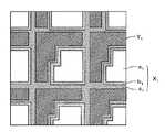
図2は、図1の発光装置の部分平面図の一例である。また、図3は、図1の発光装置の部分平面図の他の例である。これらの図において、領域Y1は、図1で基板2の上に設けられたTFT3、配線(図示せず)および蓄積容量(図示せず)などの上に、第1の絶縁膜4、陽極6、第2の絶縁膜7、有機層8および陰極9が設けられた部分である。すなわち、領域Y1は、発光部に対応する一方で、外部から入射した光に対しては不透明な部分となる。FIG. 2 is an example of a partial plan view of the light emitting device of FIG. FIG. 3 is another example of a partial plan view of the light emitting device of FIG. In these drawings, the region Y1 includes a first
一方、図2および図3において、領域a1,b1,c1からなる領域X1は、外部から入射した光に対して透明な部分である。したがって、領域X1を通して、発光装置の背面に置かれたものを視認することができる。また、領域X1で大部分の面積を占める領域a1は、図1の基板2上で、ゲート絶縁膜(図示せず)、層間絶縁膜(図示せず)および第1の絶縁膜4しか設けられていない部分である。したがって、外部から入射した光は、この発光装置を高い透過率で透過することができる。On the other hand, in FIG. 2 and FIG. 3, regionX 1 consisting regiona1, b 1,c 1 is the transparent portion relative to the incident light from the outside. Therefore, it is possible through the region X1, viewing those placed on the back of the light-emitting device. The region a1 occupying most of the area in the region X1 is only a gate insulating film (not shown), an interlayer insulating film (not shown), and the first insulating
尚、本実施の形態は図1の例に限定されるものではなく、本発明の趣旨を逸脱しない範囲内において、種々変形して実施することができる。 The present embodiment is not limited to the example shown in FIG. 1, and various modifications can be made without departing from the spirit of the present invention.
図4に、本実施の形態の変形例を示す。尚、図4において、図1と同じ符号を付した部分は同じものであることを示している。 FIG. 4 shows a modification of the present embodiment. In FIG. 4, the parts denoted by the same reference numerals as those in FIG. 1 are the same.
図4の構成は、基本的には図1の構成と同じであるが、図1では、有機層8で発光する光が一色であったのに対し、図4では、有機層8R,8G,8Bの発光色が、それぞれ赤色、緑色、青色である点で相違している。尚、有機層で発光する色の組み合わせは、これ以外であってもよい。 The configuration of FIG. 4 is basically the same as the configuration of FIG. 1, but in FIG. 1, the light emitted from the
以上述べたように、本実施の形態によれば、有機層で発光した光は、陰極側および陽極側のいずれか一方の面からのみ外部に取り出される。したがって、発光面を視認者側とすれば、背面からの発光がなくなるので、背面に出射される光に起因して視認性が低下する問題を解消することができる。また、外部から入射した光は、主として、基板上に絶縁膜のみが設けられている部分を透過するので、入射光の透過率を従来より高くすることが可能となる。 As described above, according to the present embodiment, the light emitted from the organic layer is extracted to the outside only from either one of the cathode side and the anode side. Therefore, if the light emitting surface is on the viewer side, light emission from the back surface is eliminated, so that the problem of reduced visibility due to light emitted to the back surface can be solved. In addition, since light incident from the outside mainly passes through a portion where only the insulating film is provided on the substrate, the transmittance of incident light can be made higher than before.
実施の形態2.
図5は、本実施の形態におけるアクティブマトリクスタイプの発光装置の部分断面図である。この図に示すように、発光装置11の基板12の上には、TFT(Thin Film Transistor)13が形成されており、さらに、段差被覆用の第1の絶縁膜14がTFT13の周辺に設けられている。また、第1の絶縁膜14には開口部15が設けられており、TFT13は、開口部15を通じて、第1の電極としての陽極16と電気的に接続している。尚、図では、TFT13を構成するゲート絶縁膜や層間絶縁膜、TFT13に接続する配線および蓄積容量などを省略している。
FIG. 5 is a partial cross-sectional view of the active matrix light-emitting device in this embodiment. As shown in this figure, a TFT (Thin Film Transistor) 13 is formed on the
図5に示すように、本実施の形態は、基板12上で第1の絶縁膜14が設けられていない部分20があることを特徴としている。この部分20は、例えば、第1の絶縁膜14に開口部15を形成する際に、基板12上からエッチング除去することによって形成することができる。 As shown in FIG. 5, the present embodiment is characterized in that there is a
図5において、陽極16は、TFT13の上方に設けられており、TFT13がない第1の絶縁膜14の上には設けられていない。すなわち、TFT13が配設されている位置に対応して陽極16が設けられている。また、陽極16の上には、陽極16の端面を保護するための第2の絶縁膜17が設けられている。そして、陽極16および第2の絶縁膜17の上には有機層18が設けられており、有機層18の上にはさらに第2の電極としての陰極19が設けられている。陽極16、有機層18および陰極19により、発光素子としての有機LED素子が構成される。 In FIG. 5, the
本実施の形態において、基板12、第1の絶縁膜14、第2の絶縁膜17および有機層18は、それぞれ光を透過する材料からなるものとする。また、陰極19は、光に対し透過性を有する材料からなるものとし、陽極16は、金属などの光を反射する材料からなるものとする。これにより、有機層18で発光して陰極側に出射された光は、陰極19を透過して外部に取り出される。一方、陽極側に出射された光は、陽極16で反射されて陰極側に向かった後、陰極19を透過して外部に取り出される。 In the present embodiment, the
このように、本実施の形態の発光装置では、実施の形態1と同様に、有機層で発光した光は、陰極側の面からのみ外部に取り出される。したがって、陰極側を視認者側とすれば、発光は視認者側の面でのみ起こり、発光装置の背面では起こらない。それ故、本実施の形態の発光装置によれば、背面に出射される光が迷光となって視認性を低下させる問題を解消することができる。尚、視認者側への光の取り出し効率は、発光装置を構成する部材の種類や構成を最適化することによって向上させることが可能である。 As described above, in the light emitting device of this embodiment, similarly to Embodiment 1, light emitted from the organic layer is extracted outside only from the surface on the cathode side. Therefore, if the cathode side is the viewer side, light emission occurs only on the viewer side surface and does not occur on the back surface of the light emitting device. Therefore, according to the light emitting device of the present embodiment, it is possible to solve the problem that the light emitted to the back surface becomes stray light and the visibility is lowered. Note that the light extraction efficiency to the viewer side can be improved by optimizing the type and configuration of the members constituting the light emitting device.
本実施の形態では、陰極19は、透明および半透明のいずれであってもよい。半透明にすると、光の干渉効果が大きくなるので、これを利用して視認者側への光の取り出し効率を高めることができる。また、透明電極として一般に用いられるITOは、スパッタ法による成膜が必要となるが、半透明電極として、例えば、MgAgまたはAlなどの薄膜(膜厚5nm〜15nm程度)を用いた場合には、蒸着法による成膜が可能である。蒸着法によれば、スパッタ法に比べて有機層に与えるダメージを小さくすることができるので、素子特性や信頼性を向上させる点から有利である。一方、半透明電極とした場合、発光色の角度依存性が大きくなる。したがって、用途に応じて、透明および半透明のいずれを選択するかを決めることが好ましい。 In the present embodiment, the
尚、本発明は、第1の電極を陰極とし、第2の電極を陽極としてもよい。すなわち、陰極を反射電極とし、陽極を透明電極または半透明電極としてもよい。この場合であっても、陽極側を視認者側とし、陰極側を発光装置の背面側とすれば、背面には光が出射されないので、上記と同様に視認性が低下するのを防ぐことができる。 In the present invention, the first electrode may be a cathode and the second electrode may be an anode. That is, the cathode may be a reflective electrode and the anode may be a transparent electrode or a semitransparent electrode. Even in this case, if the anode side is set as the viewer side and the cathode side is set as the back side of the light emitting device, no light is emitted to the back side. it can.
一方、外部から発光装置に入射した光は、発光装置で、TFTや電極などの光を反射する材料が用いられている部分以外の部分を透過する。例えば、図5において、発光装置11に入射した光は、TFT13および陽極16が設けられている部分以外の部分(領域X2)を透過する。これに対して、図5の領域Y2は、発光部を構成する一方で、外部から入射した光に対しては不透明な部分となる。On the other hand, light incident on the light emitting device from the outside is transmitted through the light emitting device other than the portion where a material that reflects light, such as a TFT or an electrode, is used. For example, in FIG. 5, the light incident on the
領域X2は、基板12の上に、ゲート絶縁膜(図示せず)および層間絶縁膜(図示せず)のみが形成されている部分(領域a2)と、これらの上にさらに第1の絶縁膜14が設けられている部分(領域b2)と、第1の絶縁膜14の上にさらに第2の絶縁膜17が設けられている部分(領域c2)と、第2の絶縁膜17の上にさらに有機層18および陰極19が設けられている部分(領域d2)とに大別される。この内、領域X2の面積の殆どを占めるのは領域a2であり、領域a2は、有機LED素子間で絶縁膜14が除去された部分である。The region X2 includes a portion (region a2 ) where only a gate insulating film (not shown) and an interlayer insulating film (not shown) are formed on the
実施の形態1では、光が透過する部分は、主として図1の領域a1であった。ここで、領域a1は、基板2上にゲート絶縁膜(図示せず)、層間絶縁膜(図示せず)および第1の絶縁膜4のみが設けられている部分である。一方、本実施の形態で光が透過する部分は、主として領域a2と領域b2である。ここで、領域b2は、領域a1と同様の構成物からなっているが、領域a2には、領域a1の第1の絶縁膜4に対応する膜が設けられていない。このため、領域a2を透過する光の透過率は、領域a1を透過する光の透過率より高くなる。したがって、発光装置全体としての光の透過率も、実施の形態1の透過率に比べて高くなる。In the first embodiment, the portion through which light is transmitted, was predominantly region a1 in Fig. 1. Here, the region a1 is a portion where only the gate insulating film (not shown), the interlayer insulating film (not shown), and the first insulating
このように、本実施の形態によれば、有機層で発光した光は、陰極側および陽極側のいずれか一方の面からのみ外部に取り出される。したがって、発光面を視認者側とすれば、背面には光が出射されないので、背面に出射される光に起因して視認性が低下する問題を解消することができる。また、外部から入射した光は、主として、基板上に絶縁膜のみが設けられている部分を透過するが、本実施の形態では、厚い絶縁膜(図2の第1の絶縁膜 )が形成されている部分の面積を小さくしているので、実施の形態1に比較して入射光の透過率をさらに高くすることが可能となる。 Thus, according to the present embodiment, the light emitted from the organic layer is extracted to the outside only from either one of the cathode side and the anode side. Therefore, if the light emitting surface is on the viewer side, no light is emitted to the back surface, so that the problem of reduced visibility due to the light emitted to the back surface can be solved. In addition, light incident from the outside mainly passes through a portion where only the insulating film is provided on the substrate, but in this embodiment, a thick insulating film (first insulating film in FIG. 2) is formed. Since the area of the portion is reduced, the transmittance of incident light can be further increased as compared with the first embodiment.
実施の形態3.
図6は、本実施の形態におけるアクティブマトリクスタイプの発光装置の部分断面図である。この図に示すように、発光装置21の基板22の上には、TFT(Thin Film Transistor)23が形成されており、さらに、段差被覆用の第1の絶縁膜24が設けられている。また、第1の絶縁膜24には開口部25が設けられており、TFT23は、開口部25を通じて、第1の電極としての陽極26と電気的に接続している。尚、図では、TFT23を構成するゲート絶縁膜や層間絶縁膜、TFT23に接続する配線および蓄積容量などを省略している。
FIG. 6 is a partial cross-sectional view of the active matrix light-emitting device in this embodiment. As shown in this figure, a TFT (Thin Film Transistor) 23 is formed on a
図6において、陽極26は、TFT23の上方に設けられており、TFT23がない第1の絶縁膜24の上には設けられていない。また、陽極26の上には、陽極26の端面を保護するための第2の絶縁膜27が設けられている。 In FIG. 6, the
実施の形態1や実施の形態2では、有機層は、陽極と第2の絶縁膜の上にのみ設けられていた。これに対して、本実施の形態では、有機層28が、陽極26と第2の絶縁膜27を被覆するようにして第1の絶縁膜24の上に設けられている。一方、第2の電極としての陰極29は、有機層28の上で陽極26と対向する部分に設けられており、第1の絶縁膜24と有機層28が接する部分の有機層28上には設けられていない。陽極26、有機層28および陰極29により、発光素子としての有機LED素子が構成される。 In the first embodiment and the second embodiment, the organic layer is provided only on the anode and the second insulating film. On the other hand, in this embodiment, the
本実施の形態において、基板22、第1の絶縁膜24、第2の絶縁膜27および有機層29は、それぞれ光を透過する材料からなるものとする。また、陰極29は、光に対し透過性を有する材料からなるものとし、陽極26は、金属などの光を反射する材料からなるものとする。これにより、有機層28で発光して陰極側に出射された光は、陰極29を透過して外部に取り出される。一方、陽極側に出射された光は、陽極26で反射されて陰極側に向かった後、陰極29を透過して外部に取り出される。 In the present embodiment, the
このように、本実施の形態の発光装置では、実施の形態1と同様に、有機層で発光した光は、陰極側の面からのみ外部に取り出される。したがって、陰極側を視認者側とすれば、発光は視認者側の面でのみ起こり、発光装置の背面では起こらない。それ故、本実施の形態の発光装置によれば、背面に出射される光が迷光となって視認性を低下させる問題を解消することができる。尚、視認者側への光の取り出し効率は、発光装置を構成する部材の種類や構成を最適化することによって向上させることが可能である。 As described above, in the light emitting device of this embodiment, similarly to Embodiment 1, light emitted from the organic layer is extracted outside only from the surface on the cathode side. Therefore, if the cathode side is the viewer side, light emission occurs only on the viewer side surface and does not occur on the back surface of the light emitting device. Therefore, according to the light emitting device of the present embodiment, it is possible to solve the problem that the light emitted to the back surface becomes stray light and the visibility is lowered. Note that the light extraction efficiency to the viewer side can be improved by optimizing the type and configuration of the members constituting the light emitting device.
本実施の形態では、陰極29は、透明および半透明のいずれであってもよい。半透明にすると、光の干渉効果が大きくなるので、これを利用して視認者側への光の取り出し効率を高めることができる。また、透明電極として一般に用いられるITOは、スパッタ法による成膜が必要となるが、半透明電極として、例えば、MgAgまたはAlなどの薄膜(膜厚5nm〜15nm程度)を用いた場合には、蒸着法による成膜が可能である。蒸着法によれば、スパッタ法に比べて有機層に与えるダメージを小さくすることができるので、素子特性や信頼性を向上させる点から有利である。一方、半透明電極とした場合、発光色の角度依存性が大きくなる。したがって、用途に応じて、透明および半透明のいずれを選択するかを決めることが好ましい。 In the present embodiment, the
尚、本発明は、第1の電極を陰極とし、第2の電極を陽極としてもよい。すなわち、陰極を反射電極とし、陽極を透明電極または半透明電極としてもよい。この場合であっても、陽極側を視認者側とし、陰極側を発光装置の背面側とすれば、背面には光が出射されないので、上記と同様に視認性が低下するのを防ぐことができる。 In the present invention, the first electrode may be a cathode and the second electrode may be an anode. That is, the cathode may be a reflective electrode and the anode may be a transparent electrode or a semitransparent electrode. Even in this case, if the anode side is set as the viewer side and the cathode side is set as the back side of the light emitting device, no light is emitted to the back side. it can.
一方、外部から発光装置に入射した光は、発光装置で、TFTや電極などの光を反射する材料が用いられている部分以外の部分を透過する。例えば、図6において、発光装置21に入射した光は、TFT23および陽極26が設けられている部分以外の部分(領域X3)を透過する。これに対して、図6の領域Y3は、発光部を構成する一方で、外部から入射した光に対しては不透明な部分となる。On the other hand, light incident on the light emitting device from the outside is transmitted through the light emitting device other than the portion where a material that reflects light, such as a TFT or an electrode, is used. For example, in FIG. 6, the light incident on the
領域X3は、基板22上にゲート絶縁膜(図示せず)、層間絶縁膜(図示せず)、第1の絶縁膜24およひ有機層28が設けられている部分(領域a3)と、第1の絶縁膜24と有機層28の間にさらに第2の絶縁膜27が設けられている部分(領域b3)と、領域b3の構成で有機層28の上にさらに陰極29が設けられている部分(領域c3)とに大別される。この内、占有面積が最も大きいのは領域a3であり、領域a3は、有機LED素子間で絶縁膜24の上に有機層28が形成された部分である。Region X3 is (not shown) a gate insulating film on the
本実施の形態において、光が透過する部分は、主として領域a3である。したがって、発光部を構成する構造物の全てを透過しなければならない従来例に比較すれば、入射光の透過率を高くすることができる。一方、実施の形態1における領域a1に対して、領域a3はさらに有機層が加わった構成となっているので、実施の形態1に比べると入射光の透過率は若干低下するおそれがある。しかしながら、本実施の形態の構成によれば、有機層に対して微細なパターニングを行うことが不要となるので、実施の形態1に比べて生産性を向上させることが可能となる。In this embodiment, the portion through which light is transmitted are mainly region a3. Therefore, the transmittance of incident light can be increased as compared with the conventional example that must transmit all of the structures constituting the light emitting section. On the other hand, the region a1 in the first embodiment, since the area a3 has a configuration in which further organic layer is applied, the transmittance of incident light as compared to the first embodiment may be reduced slightly . However, according to the configuration of the present embodiment, it is not necessary to perform fine patterning on the organic layer, so that productivity can be improved as compared with the first embodiment.
尚、本実施の形態は図6の例に限定されるものではなく、本発明の趣旨を逸脱しない範囲内において、種々変形して実施することができる。 Note that the present embodiment is not limited to the example of FIG. 6, and various modifications can be made without departing from the spirit of the present invention.
図7に、本実施の形態の変形例を示す。尚、図7において、図6と同じ符号を付した部分は同じものであることを示している。 FIG. 7 shows a modification of the present embodiment. In FIG. 7, the parts denoted by the same reference numerals as those in FIG. 6 are the same.
図7の構成は、基本的には図6の構成と同じであるが、図6では、有機層 で発光する光が一色であったのに対し、図7では、有機層28R,28G,28Bの発光色が、それぞれ赤色、緑色、青色である点で相違している。尚、有機層で発光する色の組み合わせは、これ以外であってもよい。 The configuration in FIG. 7 is basically the same as the configuration in FIG. 6, but in FIG. 6, the light emitted from the organic layer is one color, whereas in FIG. 7, the
以上述べたように、本実施の形態によれば、有機層で発光した光は、陰極側および陽極側のいずれか一方の面からのみ外部に取り出される。したがって、発光面を視認者側とすれば、背面からの発光がなくなるので、背面に出射される光に起因して視認性が低下する問題を解消することができる。また、外部から入射した光は、主として、基板上に絶縁膜と有機層のみが設けられている部分を透過するので、入射光の透過率を従来より高くすることが可能となる。 As described above, according to the present embodiment, the light emitted from the organic layer is extracted to the outside only from either one of the cathode side and the anode side. Therefore, if the light emitting surface is on the viewer side, light emission from the back surface is eliminated, so that the problem of reduced visibility due to light emitted to the back surface can be solved. In addition, light incident from the outside mainly passes through a portion where only the insulating film and the organic layer are provided on the substrate, so that the transmittance of incident light can be made higher than before.
実施の形態4.
図8は、本実施の形態におけるアクティブマトリクスタイプの発光装置の部分断面図である。この図に示すように、発光装置31の基板32の上には、TFT(Thin Film Transistor)33が形成されており、さらに、段差被覆用の第1の絶縁膜34が設けられている。また、第1の絶縁膜34には開口部35が設けられており、TFT33は、開口部35を通じて、第1の電極としての陽極36と電気的に接続している。尚、図では、TFT33を構成するゲート絶縁膜や層間絶縁膜、TFT33に接続する配線および蓄積容量などを省略している。
FIG. 8 is a partial cross-sectional view of the active matrix light-emitting device in this embodiment. As shown in this figure, a TFT (Thin Film Transistor) 33 is formed on a
図8において、陽極36は、TFT33の上方に設けられており、TFT33がない第1の絶縁膜34の上には設けられていない。また、陽極36の上には、陽極36の端面を保護するための第2の絶縁膜37が設けられている。そして、実施の形態3と同様に、有機層38が、陽極36と第2の絶縁膜37を被覆するようにして第1の絶縁膜34の上に設けられている。陽極36、有機層38および陰極39により、発光素子としての有機LED素子が構成される。 In FIG. 8, the
本実施の形態では、第2の電極としての陰極39が、半透明電極39aと透明電極39bの2層構造からなっていることを特徴とする。すなわち、図8に示すように、有機層38の上で陽極36と対向する部分に半透明電極39aが設けられており、半透明電極39aを被覆するようにして、有機層38の上に透明電極39bが設けられている。尚、半透明電極39aは、第1の絶縁膜34と有機層38が接する部分の有機層38の上には設けられておらず、この部分では、有機層38の上に直接透明電極39bが設けられている。 In the present embodiment, the
陰極を半透明電極とした場合、蒸着法を用いた電極形成が可能であるので、有機層に対して大きなダメージを与えずに済む。しかしながら、スパッタ法より成膜されたITOなどの透明電極と比べると、抵抗値は大きくなる傾向にある。そこで、有機層へのダメージを軽減しつつ、所望の抵抗値とするには、半透明電極の上に透明電極を設けた2層構造とするのがよい。この場合、スパッタ法により透明電極を成膜しても、有機層上に設けられた半透明電極がバリア膜として働くので、有機層へのダメージが軽減される。したがって、電気的特性および信頼性に優れた素子とすることができる。 When the cathode is a semi-transparent electrode, it is possible to form an electrode using a vapor deposition method, so that it is not necessary to give a large damage to the organic layer. However, the resistance value tends to be larger than that of a transparent electrode such as ITO formed by sputtering. Therefore, in order to obtain a desired resistance value while reducing damage to the organic layer, a two-layer structure in which a transparent electrode is provided on a semitransparent electrode is preferable. In this case, even if the transparent electrode is formed by sputtering, the translucent electrode provided on the organic layer functions as a barrier film, so that damage to the organic layer is reduced. Therefore, an element having excellent electrical characteristics and reliability can be obtained.
本実施の形態において、基板32、第1の絶縁膜34、第2の絶縁膜37および有機層38は、それぞれ光を透過する材料からなるものとする。また、陽極36は、金属などの光を反射する材料からなるものとする。上述の通り、陰極39は、半透明電極39aと透明電極39bからなるので光を透過する。したがって、有機層38で発光して陰極側に出射された光は、陰極39を透過して外部に取り出される。一方、陽極側に出射された光は、陽極36で反射されて陰極側に向かった後、陰極39を透過して外部に取り出される。 In the present embodiment, the
このように、本実施の形態の発光装置では、実施の形態1と同様に、有機層で発光した光は、陰極側の面からのみ外部に取り出される。したがって、陰極側を視認者側とすれば、発光は視認者側の面でのみ起こり、発光装置の背面では起こらない。それ故、本実施の形態の発光装置によれば、背面に出射される光が迷光となって視認性を低下させる問題を解消することができる。尚、視認者側への光の取り出し効率は、発光装置を構成する部材の種類や構成を最適化することによって向上させることが可能である。 As described above, in the light emitting device of this embodiment, similarly to Embodiment 1, light emitted from the organic layer is extracted outside only from the surface on the cathode side. Therefore, if the cathode side is the viewer side, light emission occurs only on the viewer side surface and does not occur on the back surface of the light emitting device. Therefore, according to the light emitting device of the present embodiment, it is possible to solve the problem that the light emitted to the back surface becomes stray light and the visibility is lowered. Note that the light extraction efficiency to the viewer side can be improved by optimizing the type and configuration of the members constituting the light emitting device.
尚、本発明は、第1の電極を陰極とし、第2の電極を陽極としてもよい。すなわち、陰極に光を反射する材料を用い、陽極を半透明電極と透明電極の2層構造としてもよい。この場合であっても、陽極側を視認者側とし、陰極側を発光装置の背面側とすれば、背面には光が出射されないので、上記と同様に視認性が低下するのを防ぐことができる。 In the present invention, the first electrode may be a cathode and the second electrode may be an anode. That is, a material that reflects light may be used for the cathode, and the anode may have a two-layer structure of a translucent electrode and a transparent electrode. Even in this case, if the anode side is set as the viewer side and the cathode side is set as the back side of the light emitting device, no light is emitted to the back side. it can.
一方、外部から発光装置に入射した光は、発光装置で、TFTや電極などの光を反射する材料が用いられている部分以外の部分を透過する。例えば、図8において、発光装置31に入射した光は、TFT33および陽極36が設けられている部分以外の部分(領域X4)を透過する。これに対して、図8の領域Y4は、発光部を構成する一方で、外部から入射した光に対しては不透明な部分となる。On the other hand, light incident on the light emitting device from the outside is transmitted through the light emitting device other than the portion where a material that reflects light, such as a TFT or an electrode, is used. For example, in FIG. 8, light incident on the
領域X4は、基板32上にゲート絶縁膜(図示せず)、層間絶縁膜(図示せず)、第1の絶縁膜34、有機層38および透明電極39bが設けられている部分(領域a4)と、第1の絶縁膜34と有機層38の間にさらに第2の絶縁膜37が設けられている部分(領域b4)と、領域b4の構成で有機層38と透明電極39bの間にさらに半透明電極39aが設けられている部分(領域c4)とに大別される。この内、占有面積が最も大きいのは領域a4であり、領域a4は、有機LED素子間で絶縁膜34の上に有機層38と透明電極39bが互いに接して形成された部分である。Region X4 is (not shown) a gate insulating film on a
本実施の形態において、光が透過する部分は、主として領域a4である。したがって、発光部を構成する構造物の全てを透過しなければならない従来例に比較すれば、入射光の透過率を高くすることができる。一方、実施の形態1における領域a1に対して、領域a4はさらに有機層と半透明電極が加わった構成となっているので、実施の形態1に比べると入射光の透過率は若干低下するおそれがある。しかしながら、本実施の形態の構成によれば、有機層に対して微細なパターニングを行うことが不要となるので、実施の形態1に比べて生産性を向上させることが可能となる。また、視認者側の電極を半透明電極と透明電極の2層構造としているので、電気的特性および信頼性に優れた素子とすることもできる。In this embodiment, the portion through which light is transmitted are mainly areas a4. Therefore, the transmittance of incident light can be increased as compared with the conventional example that must transmit all of the structures constituting the light emitting section. On the other hand, the region a1 in the first embodiment, since the area a4 has a configuration in which applied further organic layer and the translucent electrode, slightly decreases the transmittance of the incident light as compared with the first embodiment There is a risk. However, according to the configuration of the present embodiment, it is not necessary to perform fine patterning on the organic layer, so that productivity can be improved as compared with the first embodiment. In addition, since the viewer-side electrode has a two-layer structure of a translucent electrode and a transparent electrode, an element having excellent electrical characteristics and reliability can be obtained.
以上述べたように、本実施の形態によれば、有機層で発光した光は、陰極側および陽極側のいずれか一方の面からのみ外部に取り出される。したがって、発光面を視認者側とすれば、背面からの発光がなくなるので、背面に出射される光に起因して視認性が低下する問題を解消することができる。また、外部から入射した光が透過しなければならない構造物は従来のものより少なくて済むので、入射光の透過率を従来より高くすることが可能となる。 As described above, according to the present embodiment, the light emitted from the organic layer is extracted to the outside only from either one of the cathode side and the anode side. Therefore, if the light emitting surface is on the viewer side, light emission from the back surface is eliminated, so that the problem of reduced visibility due to light emitted to the back surface can be solved. In addition, since the number of structures to which light incident from the outside must be transmitted is smaller than that of the conventional structure, the transmittance of incident light can be made higher than that of the conventional structure.
実施の形態5.
図9は、本実施の形態におけるアクティブマトリクスタイプの発光装置の部分断面図である。この図に示すように、発光装置41の基板42の上には、TFT(Thin Film Transistor)43が形成されており、さらに、段差被覆用の第1の絶縁膜44が設けられている。また、第1の絶縁膜44には開口部45が設けられており、TFT43は、開口部45を通じて、第1の電極としての陽極46と電気的に接続している。尚、図では、TFT43を構成するゲート絶縁膜や層間絶縁膜、TFT43に接続する配線および蓄積容量などを省略している。
FIG. 9 is a partial cross-sectional view of the active matrix light-emitting device in this embodiment. As shown in this figure, a TFT (Thin Film Transistor) 43 is formed on a
図9において、陽極46は、TFT43の上方に設けられており、TFT43がない第1の絶縁膜44の上には設けられていない。また、陽極46の上には、陽極46の端面を保護するための第2の絶縁膜47が設けられている。そして、陽極46および第2の絶縁膜47の上には有機層48が設けられており、有機層48の上にはさらに半透明電極49aが設けられている。陽極46、有機層48および陰極49により、発光素子としての有機LED素子が構成される。 In FIG. 9, the anode 46 is provided above the
本実施の形態においても、実施の形態4と同様に、第2の電極としての陰極49が、半透明電極49aと透明電極49bの2層構造からなっていることを特徴とする。すなわち、図9に示すように、有機層48の上で陽極46と対向する部分に半透明電極49aが設けられており、半透明電極49aを被覆するようにして、第1の絶縁膜44の上に透明電極49bが設けられている。 Also in the present embodiment, as in the fourth embodiment, the
陰極を半透明電極とした場合、蒸着法を用いた電極形成が可能であるので、有機層に対して大きなダメージを与えずに済む。しかしながら、スパッタ法より成膜されたITOなどの透明電極と比べると、抵抗値は大きくなる傾向にある。そこで、有機層へのダメージを軽減しつつ、所望の抵抗値とするには、半透明電極の上に透明電極を設けた2層構造とするのがよい。この場合、スパッタ法により透明電極を成膜しても、有機層上に設けられた半透明電極がバリア膜として働くので、有機層へのダメージが軽減される。したがって、電気的特性および信頼性に優れた素子とすることができる。 When the cathode is a semi-transparent electrode, it is possible to form an electrode using a vapor deposition method, so that it is not necessary to give a large damage to the organic layer. However, the resistance value tends to be larger than that of a transparent electrode such as ITO formed by sputtering. Therefore, in order to obtain a desired resistance value while reducing damage to the organic layer, a two-layer structure in which a transparent electrode is provided on a semitransparent electrode is preferable. In this case, even if the transparent electrode is formed by sputtering, the translucent electrode provided on the organic layer functions as a barrier film, so that damage to the organic layer is reduced. Therefore, an element having excellent electrical characteristics and reliability can be obtained.
本実施の形態において、基板42、第1の絶縁膜44、第2の絶縁膜47および有機層48は、それぞれ光を透過する材料からなるものとする。また、陽極46は、金属などの光を反射する材料からなるものとする。上述の通り、陰極49は、半透明電極49aと透明電極49bからなるので光を透過する。したがって、有機層48で発光して陰極側に出射された光は、陰極49を透過して外部に取り出される。一方、陽極側に出射された光は、陽極46で反射されて陰極側に向かった後、陰極49を透過して外部に取り出される。 In the present embodiment, the
このように、本実施の形態の発光装置では、実施の形態1と同様に、有機層で発光した光は、陰極側の面からのみ外部に取り出される。したがって、陰極側を視認者側とすれば、発光は視認者側の面でのみ起こり、発光装置の背面では起こらない。それ故、本実施の形態の発光装置によれば、背面に出射される光が迷光となって視認性を低下させる問題を解消することができる。尚、視認者側への光の取り出し効率は、発光装置を構成する部材の種類や構成を最適化することによって向上させることが可能である。 As described above, in the light emitting device of this embodiment, similarly to Embodiment 1, light emitted from the organic layer is extracted outside only from the surface on the cathode side. Therefore, if the cathode side is the viewer side, light emission occurs only on the viewer side surface and does not occur on the back surface of the light emitting device. Therefore, according to the light emitting device of the present embodiment, it is possible to solve the problem that the light emitted to the back surface becomes stray light and the visibility is lowered. Note that the light extraction efficiency to the viewer side can be improved by optimizing the type and configuration of the members constituting the light emitting device.
尚、本発明は、第1の電極を陰極とし、第2の電極を陽極としてもよい。すなわち、陰極に光を反射する材料を用い、陽極を半透明電極と透明電極の2層構造としてもよい。この場合であっても、陽極側を視認者側とし、陰極側を発光装置の背面側とすれば、背面には光が出射されないので、上記と同様に視認性が低下するのを防ぐことができる。 In the present invention, the first electrode may be a cathode and the second electrode may be an anode. That is, a material that reflects light may be used for the cathode, and the anode may have a two-layer structure of a translucent electrode and a transparent electrode. Even in this case, if the anode side is set as the viewer side and the cathode side is set as the back side of the light emitting device, no light is emitted to the back side. it can.
一方、外部から発光装置に入射した光は、発光装置で、TFTや電極などの光を反射する材料が用いられている部分以外の部分を透過する。例えば、図9において、発光装置41に入射した光は、TFT43および陽極46が設けられている部分以外の部分(領域X5)を透過する。これに対して、図9の領域Y5は、発光部を構成する一方で、外部から入射した光に対しては不透明な部分となる。On the other hand, light incident on the light emitting device from the outside is transmitted through the light emitting device other than the portion where a material that reflects light, such as a TFT or an electrode, is used. For example, in FIG. 9, light incident on the
領域X5は、基板42上にゲート絶縁膜(図示せず)、層間絶縁膜(図示せず)、第1の絶縁膜44および透明電極49bが設けられている部分(領域a5)と、第1の絶縁膜44と透明電極49bの間にさらに第2の絶縁膜47が設けられている部分(領域b5)と、領域b5の構成で第2の絶縁膜47と透明電極49bの間にさらに有機層48と半透明電極49bが設けられている部分(領域c5)とに大別される。この内、占有面積が最も大きいのは領域a5であり、領域a5は、有機LED素子間で絶縁膜44の上に透明電極49bが形成された部分である。Region X5 is (not shown) a gate insulating film on the
本実施の形態において、光が透過する部分は、主として領域a5である。したがって、発光部を構成する構造物の全てを透過しなければならない従来例に比較すれば、入射光の透過率を高くすることができる。一方、実施の形態1における領域a1に対して、領域a5はさらに透明電極が加わった構成となっているので、実施の形態1に比べると入射光の透過率は若干低下するおそれがある。しかしながら、本実施の形態の構成によれば、視認者側の電極を半透明電極と透明電極の2層構造とすることにより、電気的特性および信頼性に優れた素子とすることができる。In this embodiment, the portion through which light is transmitted are mainly region a5. Therefore, the transmittance of incident light can be increased as compared with the conventional example that must transmit all of the structures constituting the light emitting section. On the other hand, the region a1 in the first embodiment, since the area a5 has a structure in which joined more transparent electrodes, the transmittance of incident light as compared to the first embodiment may be reduced slightly . However, according to the configuration of the present embodiment, the electrode on the viewer side has a two-layer structure of a translucent electrode and a transparent electrode, whereby an element having excellent electrical characteristics and reliability can be obtained.
以上述べたように、本実施の形態によれば、有機層で発光した光は、陰極側および陽極側のいずれか一方の面からのみ外部に取り出される。したがって、発光面を視認者側とすれば、背面からの発光がなくなるので、背面に出射される光に起因して視認性が低下する問題を解消することができる。また、外部から入射した光が透過しなければならない構造物は従来のものより少なくて済むので、入射光の透過率を従来より高くすることが可能となる。 As described above, according to the present embodiment, the light emitted from the organic layer is extracted to the outside only from either one of the cathode side and the anode side. Therefore, if the light emitting surface is on the viewer side, light emission from the back surface is eliminated, so that the problem of reduced visibility due to light emitted to the back surface can be solved. In addition, since the number of structures to which light incident from the outside must be transmitted is smaller than that of the conventional structure, the transmittance of incident light can be made higher than that of the conventional structure.
実施の形態6.
図10は、本実施の形態におけるセグメントタイプの発光装置の部分断面図である。この図に示すように、発光装置51の基板52の上には、第1の電極としての陽極53が形成されており、さらに、陽極53の間には素子分離用の絶縁膜54が、陽極53の縁部を覆うように設けられている。また、絶縁膜54および陽極53の上には有機層55が設けられている。陽極53、有機層55および陰極56により、発光素子としての有機LED素子が構成される。また、陽極53の1つと、これに対応する位置に設けられた陰極56の1つと、これらに挟持された有機層55とによって1画素が構成される。
FIG. 10 is a partial cross-sectional view of the segment type light-emitting device in the present embodiment. As shown in this figure, an
本実施の形態においては、透過率向上の観点から、第2の電極としての陰極56の幅を従来より狭くすることが好ましい。具体的には、陰極53の幅を、画素ピッチの20%〜40%程度とすることが好ましい。例えば、従来の同じ仕様のものに対して、1/4程度の幅とすることができる。 In the present embodiment, it is preferable to make the width of the
基板52、絶縁膜54、陽極53および有機層55には、全て透明な材料を用いる。一方、陰極56には、金属などの光を反射する材料を用いる。これにより、有機層55で発光して陽極側に出射された光は、陽極53を透過して外部に取り出される。一方、陰極側に出射された光は、陰極56で反射されて陽極側に向かった後、陽極53を透過して外部に取り出される。 The
このように、本実施の形態の発光装置では、有機層で発光した光は、陽極側の面からのみ外部に取り出される。したがって、陽極側を視認者側とすれば、発光は視認者側の面でのみ起こるので、背面に出射される光が迷光となって視認性を低下させる問題を解消することができる。尚、視認者側への光の取り出し効率は、発光装置を構成する部材の種類や構成を最適化することによって向上させることが可能である。 Thus, in the light emitting device of this embodiment, light emitted from the organic layer is extracted outside only from the surface on the anode side. Therefore, if the anode side is the viewer side, light emission occurs only on the viewer side surface, so that the problem that the light emitted to the back surface becomes stray light and the visibility is lowered can be solved. Note that the light extraction efficiency to the viewer side can be improved by optimizing the type and configuration of the members constituting the light emitting device.
尚、本発明は、第1の電極を陰極とし、第2の電極を陽極としてもよい。すなわち、陽極を反射電極とし、陰極を透明電極とすることもできる。この場合であっても、陰極側を視認者側とし、陽極側を発光装置の背面側とすれば、背面には光が出射されないので、上記と同様に視認性が低下するのを防ぐことができる。 In the present invention, the first electrode may be a cathode and the second electrode may be an anode. That is, the anode can be a reflective electrode and the cathode can be a transparent electrode. Even in this case, if the cathode side is set as the viewer side and the anode side is set as the back side of the light emitting device, no light is emitted to the back side. it can.
一方、外部から発光装置に入射した光は、光を反射する材料が用いられた部分以外の部分を透過する。例えば、図10において、発光装置51に入射した光は、陰極56が設けられていない部分(領域X6)を透過する。領域X6は、陰極56間で有機層55が露出した部分と言い換えることもできる。これに対して、図10の領域Y6は、発光部を構成する一方で、外部から入射した光に対しては不透明な部分となる。On the other hand, light incident on the light emitting device from the outside passes through a portion other than a portion where a material that reflects light is used. For example, in FIG. 10, the light incident on the
図11は、図10の発光装置の部分平面図の一例である。尚、図11でA−A′線に沿う断面図が図10の対応する。 FIG. 11 is an example of a partial plan view of the light-emitting device of FIG. Note that a sectional view taken along the line AA ′ in FIG. 11 corresponds to FIG. 10.
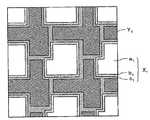
図11において、領域Y6は、図10で基板52の上に、陽極53、有機層55および陰極56が設けられた部分である。すなわち、領域Y6は、発光部に対応する一方で、外部から入射した光に対しては不透明な部分となる。これに対して、領域X6は、領域a6と領域b6からなる。ここで、領域a6は、基板52の上に、陽極53と有機層55が形成された部分である。また、領域b6は、基板52の上に、絶縁膜54と有機層55が形成された部分である。つまり、領域X6には、光を反射する陰極56が設けられていないので、この領域は、外部から入射した光に対して透明な部分となる。11, regionY 6 is, on the
図13で説明したように、従来の発光装置では、発光部および非発光部がともに光の透過する部分となっている。この構造では、非発光部にも陰極206が設けられているので、光は、基板202、陽極203、絶縁膜204および有機層205以外に陰極206も透過しなければならず、透過率を一定値以上にするのには限界があった。 As described with reference to FIG. 13, in the conventional light emitting device, both the light emitting portion and the non-light emitting portion are light transmitting portions. In this structure, since the
しかし、本実施の形態によれば、外部から入射した光は、陰極が設けられていない部分を透過するので、従来よりも透過率を高くすることが可能である。尚、発光部は光を透過しないので、発光部および非発光部の両方が光を透過する従来品に比べると、光を透過する部分の面積は、本実施の形態のものの方が小さくなる。これについては、上述したように、陰極の幅を従来より狭くすることで対処が可能である。 However, according to the present embodiment, the light incident from the outside passes through the portion where the cathode is not provided, so that the transmittance can be increased as compared with the conventional case. Since the light emitting part does not transmit light, the area of the light transmitting part is smaller in the embodiment than in the conventional product in which both the light emitting part and the non-light emitting part transmit light. As described above, this can be dealt with by making the width of the cathode narrower than before.
以上述べたように、本実施の形態によれば、有機層で発光した光は、陰極側および陽極側のいずれか一方の面からのみ外部に取り出される。したがって、発光面を視認者側とすれば、背面からの発光がなくなるので、背面に出射される光に起因して視認性が低下する問題を解消することができる。 As described above, according to the present embodiment, the light emitted from the organic layer is extracted to the outside only from either one of the cathode side and the anode side. Therefore, if the light emitting surface is on the viewer side, light emission from the back surface is eliminated, so that the problem of reduced visibility due to light emitted to the back surface can be solved.
また、本実施の形態によれば、外部から入射した光は、陰極が設けられていない部分を透過するので、入射光の透過率を従来より高くすることが可能となる。また、陰極を反射電極とした場合には、Al(アルミニウム)等の金属を用いることができるので、低抵抗化が可能となる。 In addition, according to the present embodiment, the light incident from the outside passes through the portion where the cathode is not provided, so that the transmittance of the incident light can be made higher than before. When the cathode is a reflective electrode, a metal such as Al (aluminum) can be used, so that the resistance can be reduced.
さらに、本実施の形態の発光装置には、従来のボトムエミッション型の素子構成やプロセスを活かすことができるので、透明な素子を新たに開発する場合に比べると、素子の特性や寿命を向上させる点で有利である。 Furthermore, since the light emitting device of this embodiment can take advantage of the conventional bottom emission type element configuration and process, the characteristics and lifetime of the element are improved as compared with the case where a transparent element is newly developed. This is advantageous.
尚、本発明は、上記各実施の形態に限定されるものではなく、本発明の趣旨を逸脱しない範囲内において、種々変形して実施することができる。 The present invention is not limited to the above embodiments, and various modifications can be made without departing from the spirit of the present invention.
例えば、実施の形態1〜6では、発光素子として有機LED素子を用いたが、本発明は、無機LED素子を用いてもよい。また、他の反射型の発光装置に適用することも可能である。 For example, in Embodiments 1 to 6, an organic LED element is used as a light emitting element, but an inorganic LED element may be used in the present invention. Further, the present invention can be applied to other reflective light emitting devices.
また、実施の形態1〜5のアクティブマトリクス型発光装置は、基板の上方に光が出射されるトップエミッションタイプであったが、本発明は、基板の下方に光が出射されるボトムエミッションタイプであってもよい。同様に、実施の形態6のセグメント型発光装置では、ボトムエミッションタイプであったが、本発明はトップエミッションタイプのセグメント型発光装置であってもよい。 In addition, the active matrix light-emitting devices of Embodiments 1 to 5 are top emission types in which light is emitted above the substrate, but the present invention is a bottom emission type in which light is emitted below the substrate. There may be. Similarly, although the segment type light emitting device of the sixth embodiment is the bottom emission type, the present invention may be a top emission type segment type light emitting device.
1,11,21,31,41,51 発光装置
2,12,22,32,42,52,102,202 基板
3,13,23,33,43,103 TFT
4,14,24,34,44,104 第1の絶縁膜
5,15,25,35,45,105 開口部
6,16,26,36,46,53,106,203 陽極
7,17,27,37,47,107 第2の絶縁膜
54,204 絶縁膜
8,18,28,38,48,55,108,205 有機層
9,19,29,39,49,56,109,206 陰極1, 11, 21, 31, 41, 51 Light-emitting
4, 14, 24, 34, 44, 104
Claims (8)
Translated fromJapanese前記基板の上に設けられて前記薄膜トランジスタを被覆する絶縁膜と、
光を反射する第1の電極と光を透過する第2の電極の間に発光層が挟持された構造を有し、前記絶縁膜に設けられた開口部を介して前記薄膜トランジスタに前記第1の電極が電気的に接続する複数の発光素子とを備えた発光装置であって、
前記発光素子間には前記絶縁膜が露出した部分があり、外部から入射した光は、主としてこの部分を透過することを特徴とする表示装置。A plurality of thin film transistors provided on a substrate;
An insulating film provided on the substrate and covering the thin film transistor;
A light emitting layer is sandwiched between a first electrode that reflects light and a second electrode that transmits light, and the first thin film transistor is connected to the thin film transistor through an opening provided in the insulating film. A light-emitting device comprising a plurality of light-emitting elements to which electrodes are electrically connected,
There is a portion where the insulating film is exposed between the light emitting elements, and light incident from the outside mainly transmits through this portion.
前記基板の上に設けられて前記薄膜トランジスタを被覆する絶縁膜と、
光を反射する第1の電極と光を透過する第2の電極の間に発光層が挟持された構造を有し、前記絶縁膜に設けられた開口部を介して前記薄膜トランジスタに前記第1の電極が電気的に接続する複数の発光素子とを備えた発光装置であって、
前記発光素子間には前記絶縁膜が除去された部分があり、外部から入射した光は、主としてこの部分を透過することを特徴とする表示装置。A plurality of thin film transistors provided on a substrate;
An insulating film provided on the substrate and covering the thin film transistor;
A light emitting layer is sandwiched between a first electrode that reflects light and a second electrode that transmits light, and the first thin film transistor is connected to the thin film transistor through an opening provided in the insulating film. A light-emitting device comprising a plurality of light-emitting elements to which electrodes are electrically connected,
There is a portion where the insulating film is removed between the light emitting elements, and light incident from the outside mainly transmits through this portion.
前記基板の上に設けられて前記薄膜トランジスタを被覆する絶縁膜と、
光を反射する第1の電極と光を透過する第2の電極の間に発光層が挟持された構造を有し、前記絶縁膜に設けられた開口部を介して前記薄膜トランジスタに前記第1の電極が電気的に接続する複数の発光素子とを備えた発光装置であって、
前記発光素子間には、前記絶縁膜の上に前記発光層が形成された部分があり、外部から入射した光は、主としてこの部分を透過することを特徴とする表示装置。A plurality of thin film transistors provided on a substrate;
An insulating film provided on the substrate and covering the thin film transistor;
A light emitting layer is sandwiched between a first electrode that reflects light and a second electrode that transmits light, and the first thin film transistor is connected to the thin film transistor through an opening provided in the insulating film. A light-emitting device comprising a plurality of light-emitting elements to which electrodes are electrically connected,
Between the light emitting elements, there is a portion where the light emitting layer is formed on the insulating film, and light incident from the outside mainly transmits through this portion.
前記基板の上に設けられて前記薄膜トランジスタを被覆する絶縁膜と、
光を反射する第1の電極と光を透過する第2の電極の間に発光層が挟持された構造を有し、前記絶縁膜に設けられた開口部を介して前記薄膜トランジスタに前記第1の電極が電気的に接続する複数の発光素子とを備えた発光装置であって、
前記第2の電極は、前記発光層の側から順に半透明電極と透明電極が積層された構造を有していて、
前記発光素子間には、前記絶縁膜の上に前記発光層と前記透明電極が互いに接して形成された部分があり、外部から入射した光は、主としてこの部分を透過することを特徴とする表示装置。A plurality of thin film transistors provided on a substrate;
An insulating film provided on the substrate and covering the thin film transistor;
A light emitting layer is sandwiched between a first electrode that reflects light and a second electrode that transmits light, and the first thin film transistor is connected to the thin film transistor through an opening provided in the insulating film. A light-emitting device comprising a plurality of light-emitting elements to which electrodes are electrically connected,
The second electrode has a structure in which a semitransparent electrode and a transparent electrode are laminated in order from the light emitting layer side,
Between the light emitting elements, there is a portion where the light emitting layer and the transparent electrode are formed in contact with each other on the insulating film, and light incident from the outside mainly transmits through this portion. apparatus.
前記基板の上に設けられて前記薄膜トランジスタを被覆する絶縁膜と、
光を反射する第1の電極と光を透過する第2の電極の間に発光層が挟持された構造を有し、前記絶縁膜に設けられた開口部を介して前記薄膜トランジスタに前記第1の電極が電気的に接続する複数の発光素子とを備えた発光装置であって、
前記第2の電極は、前記発光層の側から順に半透明電極と透明電極が積層された構造を有していて、
前記発光素子間には、前記絶縁膜の上に前記透明電極が形成された部分があり、外部から入射した光は、主としてこの部分を透過することを特徴とする表示装置。A plurality of thin film transistors provided on a substrate;
An insulating film provided on the substrate and covering the thin film transistor;
A light emitting layer is sandwiched between a first electrode that reflects light and a second electrode that transmits light, and the first thin film transistor is connected to the thin film transistor through an opening provided in the insulating film. A light-emitting device comprising a plurality of light-emitting elements to which electrodes are electrically connected,
The second electrode has a structure in which a semitransparent electrode and a transparent electrode are laminated in order from the light emitting layer side,
Between the light emitting elements, there is a portion where the transparent electrode is formed on the insulating film, and light incident from the outside mainly transmits through this portion.
前記第1の電極間に設けられた絶縁膜と、
前記第1の電極と前記絶縁膜の上に設けられた発光層と、
前記発光層の上に設けられ、光を反射する複数の第2の電極とを備えた発光装置であって、
前記第2の電極間には前記発光層が露出した部分があり、外部から入射した光は、主としてこの部分を透過することを特徴とする表示装置。A plurality of first electrodes provided on the substrate and transmitting light;
An insulating film provided between the first electrodes;
A light emitting layer provided on the first electrode and the insulating film;
A light emitting device including a plurality of second electrodes provided on the light emitting layer and reflecting light,
There is a portion where the light emitting layer is exposed between the second electrodes, and light incident from the outside is mainly transmitted through this portion.
前記第2の電極の幅は、前記画素のピッチの20%〜40%の範囲であることを特徴とする請求項6に記載の発光装置。A pixel comprising one of the first electrodes, one of the second electrodes provided at a position corresponding to the first electrode, and the light emitting layer sandwiched between the first electrode and the second electrode Has a structure in which a plurality of are arranged,
The light emitting device according to claim 6, wherein the width of the second electrode is in a range of 20% to 40% of the pitch of the pixels.
Priority Applications (1)
| Application Number | Priority Date | Filing Date | Title |
|---|---|---|---|
| JP2006296575AJP5106823B2 (en) | 2006-10-31 | 2006-10-31 | Light emitting device |
Applications Claiming Priority (1)
| Application Number | Priority Date | Filing Date | Title |
|---|---|---|---|
| JP2006296575AJP5106823B2 (en) | 2006-10-31 | 2006-10-31 | Light emitting device |
Publications (2)
| Publication Number | Publication Date |
|---|---|
| JP2008112112Atrue JP2008112112A (en) | 2008-05-15 |
| JP5106823B2 JP5106823B2 (en) | 2012-12-26 |
Family
ID=39444642
Family Applications (1)
| Application Number | Title | Priority Date | Filing Date |
|---|---|---|---|
| JP2006296575AExpired - Fee RelatedJP5106823B2 (en) | 2006-10-31 | 2006-10-31 | Light emitting device |
Country Status (1)
| Country | Link |
|---|---|
| JP (1) | JP5106823B2 (en) |
Cited By (43)
| Publication number | Priority date | Publication date | Assignee | Title |
|---|---|---|---|---|
| CN101958340A (en)* | 2009-07-20 | 2011-01-26 | 三星移动显示器株式会社 | Organic Light Emitting Diode Display |
| CN102130148A (en)* | 2009-12-21 | 2011-07-20 | 三星移动显示器株式会社 | Organic Light Emitting Diode Display |
| CN102194854A (en)* | 2010-03-10 | 2011-09-21 | 三星移动显示器株式会社 | Organic light emitting display device and method of manufacturing the same |
| JP2011186427A (en)* | 2010-03-05 | 2011-09-22 | Samsung Mobile Display Co Ltd | Organic light emitting display device |
| KR101084189B1 (en) | 2010-01-21 | 2011-11-17 | 삼성모바일디스플레이주식회사 | Organic light emitting display |
| KR101097335B1 (en) | 2010-02-25 | 2011-12-23 | 삼성모바일디스플레이주식회사 | Method for manufacturing organic light emitting display device |
| JP2012015092A (en)* | 2010-07-02 | 2012-01-19 | Samsung Mobile Display Co Ltd | Organic light emitting display device |
| KR101108170B1 (en)* | 2010-03-15 | 2012-01-31 | 삼성모바일디스플레이주식회사 | OLED display and manufacturing method thereof |
| CN102456713A (en)* | 2010-10-28 | 2012-05-16 | 三星移动显示器株式会社 | Organic light emitting display device and method of manufacturing the same |
| KR101147423B1 (en)* | 2010-05-06 | 2012-05-22 | 삼성모바일디스플레이주식회사 | Organic light emitting diode display |
| KR101146988B1 (en)* | 2010-05-04 | 2012-05-22 | 삼성모바일디스플레이주식회사 | Organic light emitting display device |
| KR101156434B1 (en)* | 2010-01-05 | 2012-06-18 | 삼성모바일디스플레이주식회사 | Organic light emitting display device |
| KR101156435B1 (en)* | 2010-01-08 | 2012-06-18 | 삼성모바일디스플레이주식회사 | Organic light emitting display device |
| JP2012134118A (en)* | 2010-12-20 | 2012-07-12 | Samsung Mobile Display Co Ltd | Organic light-emitting display device |
| KR101223722B1 (en)* | 2010-04-02 | 2013-01-17 | 삼성디스플레이 주식회사 | Organic light emitting display device |
| KR101223727B1 (en)* | 2012-03-29 | 2013-01-17 | 삼성디스플레이 주식회사 | Organic light emitting display device and manufacturing method thereof |
| KR101243925B1 (en)* | 2012-04-06 | 2013-03-15 | 삼성디스플레이 주식회사 | Organic light emitting display device |
| KR20130102798A (en)* | 2012-03-08 | 2013-09-23 | 주성엔지니어링(주) | An assembly comprising aa light emitting module and a manufacturing method thereof |
| US8625055B2 (en) | 2010-04-01 | 2014-01-07 | Samsung Display Co., Ltd. | Organic light emitting display device |
| KR101397110B1 (en) | 2010-10-28 | 2014-05-19 | 삼성디스플레이 주식회사 | Organic light emitting display device and manufacturing method thereof |
| WO2014119058A1 (en)* | 2013-02-04 | 2014-08-07 | 株式会社 東芝 | Organic electroluminescent element, lighting device and lighting system |
| CN104201292A (en)* | 2014-08-27 | 2014-12-10 | 京东方科技集团股份有限公司 | Organic electroluminescent device and manufacturing method thereof |
| US8952998B2 (en) | 2012-02-14 | 2015-02-10 | Samsung Display Co., Ltd. | Organic light emitting display apparatus |
| CN104377310A (en)* | 2013-08-12 | 2015-02-25 | 三星显示有限公司 | Display device |
| JP2015079758A (en)* | 2013-10-18 | 2015-04-23 | 三星ディスプレイ株式會社Samsung Display Co.,Ltd. | Organic light-emitting display device |
| US9214499B2 (en) | 2013-02-12 | 2015-12-15 | Samsung Display Co., Ltd. | Organic light emitting display device |
| US9245936B2 (en) | 2012-11-19 | 2016-01-26 | Samsung Display Co., Ltd. | Multi-display apparatus |
| KR20160068592A (en)* | 2014-12-05 | 2016-06-15 | 엘지디스플레이 주식회사 | Transparent organic light emitting display device and method of manufacturing the same |
| US9418588B2 (en) | 2013-06-13 | 2016-08-16 | Samsung Display Co., Ltd. | Flat panel display device and method to control the same |
| KR20160101271A (en)* | 2015-02-16 | 2016-08-25 | 삼성디스플레이 주식회사 | Display device |
| KR20160106540A (en)* | 2016-09-01 | 2016-09-12 | 엘지디스플레이 주식회사 | Organic Light Emitting Display |
| CN106097979A (en)* | 2015-04-28 | 2016-11-09 | 乐金显示有限公司 | Transparent display and transparent display panel |
| JP2017040876A (en)* | 2015-08-21 | 2017-02-23 | 株式会社ジャパンディスプレイ | Display device |
| KR101801912B1 (en)* | 2017-02-21 | 2017-12-29 | 삼성디스플레이 주식회사 | Organic light emitting display device |
| JPWO2017073459A1 (en)* | 2015-10-27 | 2018-09-06 | パイオニア株式会社 | Light emitting system |
| US10199611B2 (en) | 2011-12-23 | 2019-02-05 | Samsung Display Co., Ltd. | Organic light-emitting display apparatus and method of manufacturing the same |
| KR101918751B1 (en)* | 2017-12-07 | 2019-02-11 | 삼성디스플레이 주식회사 | Organic light emitting display device |
| JP2019046807A (en)* | 2018-12-19 | 2019-03-22 | パイオニア株式会社 | Light-emitting device |
| KR20200027600A (en)* | 2018-09-04 | 2020-03-13 | 삼성디스플레이 주식회사 | Display apparatus and manufacturing method thereof |
| CN111596783A (en)* | 2019-02-20 | 2020-08-28 | 三星显示有限公司 | display screen |
| CN114695502A (en)* | 2021-09-16 | 2022-07-01 | 友达光电股份有限公司 | display panel |
| JP2022176326A (en)* | 2013-09-13 | 2022-11-25 | 株式会社半導体エネルギー研究所 | light emitting device |
| US11611055B2 (en) | 2015-02-24 | 2023-03-21 | Samsung Display Co., Ltd. | Organic light emitting display device with conductive protection layers that are spaced apart from each other and method of manufacturing the same |
Families Citing this family (1)
| Publication number | Priority date | Publication date | Assignee | Title |
|---|---|---|---|---|
| KR102829301B1 (en) | 2020-07-21 | 2025-07-04 | 삼성디스플레이 주식회사 | Electronic device and method of manufacturing the same |
Citations (14)
| Publication number | Priority date | Publication date | Assignee | Title |
|---|---|---|---|---|
| JPH0256893A (en)* | 1988-08-23 | 1990-02-26 | Nec Kansai Ltd | Thin film el panel |
| JPH0773971A (en)* | 1993-09-03 | 1995-03-17 | Sharp Corp | EL element |
| JPH10214042A (en)* | 1996-11-29 | 1998-08-11 | Sanyo Electric Co Ltd | Display device |
| JPH11160704A (en)* | 1997-11-26 | 1999-06-18 | Casio Comput Co Ltd | Display device |
| JP2000012235A (en)* | 1998-06-23 | 2000-01-14 | Casio Comput Co Ltd | EL element |
| JP2001148292A (en)* | 1999-09-08 | 2001-05-29 | Denso Corp | Organic EL device |
| WO2001047322A1 (en)* | 1999-12-22 | 2001-06-28 | Sony Corporation | Organic electroluminescence display |
| JP2001230072A (en)* | 2000-02-18 | 2001-08-24 | Denso Corp | Organic el display device |
| JP2003017272A (en)* | 2001-07-03 | 2003-01-17 | Sony Corp | Display device and method of manufacturing display device |
| JP2003229283A (en)* | 2002-02-04 | 2003-08-15 | Toshiba Corp | Flat display device and method of manufacturing the same |
| JP2004184838A (en)* | 2002-12-05 | 2004-07-02 | Denso Corp | Fitting structure for composite display device |
| JP2004206927A (en)* | 2002-12-24 | 2004-07-22 | Denso Corp | Transparent el display device |
| JP2005011572A (en)* | 2003-06-17 | 2005-01-13 | Seiko Epson Corp | ORGANIC EL DEVICE, ITS MANUFACTURING METHOD, AND ELECTRONIC DEVICE |
| WO2005088594A1 (en)* | 2004-03-12 | 2005-09-22 | Fujitsu Limited | Display and method for driving same |
- 2006
- 2006-10-31JPJP2006296575Apatent/JP5106823B2/ennot_activeExpired - Fee Related
Patent Citations (14)
| Publication number | Priority date | Publication date | Assignee | Title |
|---|---|---|---|---|
| JPH0256893A (en)* | 1988-08-23 | 1990-02-26 | Nec Kansai Ltd | Thin film el panel |
| JPH0773971A (en)* | 1993-09-03 | 1995-03-17 | Sharp Corp | EL element |
| JPH10214042A (en)* | 1996-11-29 | 1998-08-11 | Sanyo Electric Co Ltd | Display device |
| JPH11160704A (en)* | 1997-11-26 | 1999-06-18 | Casio Comput Co Ltd | Display device |
| JP2000012235A (en)* | 1998-06-23 | 2000-01-14 | Casio Comput Co Ltd | EL element |
| JP2001148292A (en)* | 1999-09-08 | 2001-05-29 | Denso Corp | Organic EL device |
| WO2001047322A1 (en)* | 1999-12-22 | 2001-06-28 | Sony Corporation | Organic electroluminescence display |
| JP2001230072A (en)* | 2000-02-18 | 2001-08-24 | Denso Corp | Organic el display device |
| JP2003017272A (en)* | 2001-07-03 | 2003-01-17 | Sony Corp | Display device and method of manufacturing display device |
| JP2003229283A (en)* | 2002-02-04 | 2003-08-15 | Toshiba Corp | Flat display device and method of manufacturing the same |
| JP2004184838A (en)* | 2002-12-05 | 2004-07-02 | Denso Corp | Fitting structure for composite display device |
| JP2004206927A (en)* | 2002-12-24 | 2004-07-22 | Denso Corp | Transparent el display device |
| JP2005011572A (en)* | 2003-06-17 | 2005-01-13 | Seiko Epson Corp | ORGANIC EL DEVICE, ITS MANUFACTURING METHOD, AND ELECTRONIC DEVICE |
| WO2005088594A1 (en)* | 2004-03-12 | 2005-09-22 | Fujitsu Limited | Display and method for driving same |
Cited By (98)
| Publication number | Priority date | Publication date | Assignee | Title |
|---|---|---|---|---|
| KR101107178B1 (en)* | 2009-07-20 | 2012-01-25 | 삼성모바일디스플레이주식회사 | Organic light emitting display |
| JP2011023340A (en)* | 2009-07-20 | 2011-02-03 | Samsung Mobile Display Co Ltd | Organic light-emitting display device |
| CN101958340B (en)* | 2009-07-20 | 2013-08-14 | 三星显示有限公司 | Organic light emitting diode display |
| CN101958340A (en)* | 2009-07-20 | 2011-01-26 | 三星移动显示器株式会社 | Organic Light Emitting Diode Display |
| US8587499B2 (en) | 2009-07-20 | 2013-11-19 | Samsung Display Co., Ltd. | Organic light emitting diode display |
| KR101084240B1 (en)* | 2009-12-21 | 2011-11-16 | 삼성모바일디스플레이주식회사 | Organic light emitting diode display |
| CN102130148A (en)* | 2009-12-21 | 2011-07-20 | 三星移动显示器株式会社 | Organic Light Emitting Diode Display |
| US8558222B2 (en) | 2009-12-21 | 2013-10-15 | Samsung Display Co., Ltd. | Organic light emitting diode display |
| US8638030B2 (en) | 2010-01-05 | 2014-01-28 | Samsung Display Co., Ltd. | Organic light emitting display device including pixel electrode not formed in light transmissive region |
| KR101156434B1 (en)* | 2010-01-05 | 2012-06-18 | 삼성모바일디스플레이주식회사 | Organic light emitting display device |
| KR101156435B1 (en)* | 2010-01-08 | 2012-06-18 | 삼성모바일디스플레이주식회사 | Organic light emitting display device |
| US8659218B2 (en) | 2010-01-08 | 2014-02-25 | Samsung Display Co., Ltd. | Organic light emitting display device |
| KR101084189B1 (en) | 2010-01-21 | 2011-11-17 | 삼성모바일디스플레이주식회사 | Organic light emitting display |
| US8530910B2 (en) | 2010-01-21 | 2013-09-10 | Samsung Display Co., Ltd. | Organic light emitting display device including transmitting regions between pixel regions |
| KR101097335B1 (en) | 2010-02-25 | 2011-12-23 | 삼성모바일디스플레이주식회사 | Method for manufacturing organic light emitting display device |
| US8435810B2 (en) | 2010-02-25 | 2013-05-07 | Samsung Display Co., Ltd. | Method of manufacturing organic light emitting display device |
| JP2011186427A (en)* | 2010-03-05 | 2011-09-22 | Samsung Mobile Display Co Ltd | Organic light emitting display device |
| CN102194854A (en)* | 2010-03-10 | 2011-09-21 | 三星移动显示器株式会社 | Organic light emitting display device and method of manufacturing the same |
| US9847486B2 (en) | 2010-03-10 | 2017-12-19 | Samsung Display Co., Ltd. | Method of manufacturing organic light emitting display device |
| US9490311B2 (en) | 2010-03-10 | 2016-11-08 | Samsung Display Co., Ltd. | Organic light emitting display device and method of manufacturing the same |
| USRE49965E1 (en) | 2010-03-10 | 2024-05-07 | Samsung Display Co., Ltd. | Display device and manufacturing method thereof |
| USRE50487E1 (en) | 2010-03-10 | 2025-07-08 | Samsung Display Co., Ltd. | Display device and manufacturing method thereof |
| US8193017B2 (en) | 2010-03-15 | 2012-06-05 | Samsung Mobile Display Co., Ltd. | Organic light emitting display device and method of manufacturing the same |
| US8796702B2 (en) | 2010-03-15 | 2014-08-05 | Samsung Display Co., Ltd. | Organic light emitting display device |
| KR101108170B1 (en)* | 2010-03-15 | 2012-01-31 | 삼성모바일디스플레이주식회사 | OLED display and manufacturing method thereof |
| US8625055B2 (en) | 2010-04-01 | 2014-01-07 | Samsung Display Co., Ltd. | Organic light emitting display device |
| US8835926B2 (en) | 2010-04-02 | 2014-09-16 | Samsung Display Co., Ltd. | Organic light emitting display device |
| KR101223722B1 (en)* | 2010-04-02 | 2013-01-17 | 삼성디스플레이 주식회사 | Organic light emitting display device |
| US8963129B2 (en) | 2010-05-04 | 2015-02-24 | Samsung Display Co., Ltd. | Organic light emitting display device |
| KR101146988B1 (en)* | 2010-05-04 | 2012-05-22 | 삼성모바일디스플레이주식회사 | Organic light emitting display device |
| KR101147423B1 (en)* | 2010-05-06 | 2012-05-22 | 삼성모바일디스플레이주식회사 | Organic light emitting diode display |
| US9219103B2 (en) | 2010-05-06 | 2015-12-22 | Samsung Display Co., Ltd. | Organic light emitting diode display |
| KR101193195B1 (en)* | 2010-07-02 | 2012-10-19 | 삼성디스플레이 주식회사 | Organic light emitting display |
| JP2012015092A (en)* | 2010-07-02 | 2012-01-19 | Samsung Mobile Display Co Ltd | Organic light emitting display device |
| US8569762B2 (en) | 2010-07-02 | 2013-10-29 | Samsung Display Co., Ltd. | Organic light-emitting display device having improved transmittance |
| US9287339B2 (en) | 2010-10-28 | 2016-03-15 | Samsung Display Co., Ltd. | Organic light emitting display device and method of manufacturing the same |
| CN102456713A (en)* | 2010-10-28 | 2012-05-16 | 三星移动显示器株式会社 | Organic light emitting display device and method of manufacturing the same |
| TWI549284B (en)* | 2010-10-28 | 2016-09-11 | 三星顯示器有限公司 | Organic light emitting display device and method of manufacturing the same |
| US9761647B2 (en) | 2010-10-28 | 2017-09-12 | Samsung Display Co., Ltd. | Organic light emitting display device and method of manufacturing the same |
| CN102456713B (en)* | 2010-10-28 | 2016-01-13 | 三星显示有限公司 | Organic light-emitting display device and manufacture method thereof |
| KR101397110B1 (en) | 2010-10-28 | 2014-05-19 | 삼성디스플레이 주식회사 | Organic light emitting display device and manufacturing method thereof |
| JP2012134118A (en)* | 2010-12-20 | 2012-07-12 | Samsung Mobile Display Co Ltd | Organic light-emitting display device |
| US10199611B2 (en) | 2011-12-23 | 2019-02-05 | Samsung Display Co., Ltd. | Organic light-emitting display apparatus and method of manufacturing the same |
| US11394015B2 (en) | 2011-12-23 | 2022-07-19 | Samsung Display Co., Ltd. | Organic light-emitting display apparatus and method of manufacturing the same |
| US10840481B2 (en) | 2011-12-23 | 2020-11-17 | Samsung Display Co., Ltd. | Organic light-emitting display apparatus and method of manufacturing the same |
| US8952998B2 (en) | 2012-02-14 | 2015-02-10 | Samsung Display Co., Ltd. | Organic light emitting display apparatus |
| KR101883322B1 (en)* | 2012-03-08 | 2018-07-31 | 주성엔지니어링(주) | An assembly comprising aa light emitting module and a manufacturing method thereof |
| KR20130102798A (en)* | 2012-03-08 | 2013-09-23 | 주성엔지니어링(주) | An assembly comprising aa light emitting module and a manufacturing method thereof |
| KR101223727B1 (en)* | 2012-03-29 | 2013-01-17 | 삼성디스플레이 주식회사 | Organic light emitting display device and manufacturing method thereof |
| KR101243925B1 (en)* | 2012-04-06 | 2013-03-15 | 삼성디스플레이 주식회사 | Organic light emitting display device |
| US9245936B2 (en) | 2012-11-19 | 2016-01-26 | Samsung Display Co., Ltd. | Multi-display apparatus |
| JP2014154211A (en)* | 2013-02-04 | 2014-08-25 | Toshiba Corp | Organic electroluminescent element, illumination device and illumination system |
| WO2014119058A1 (en)* | 2013-02-04 | 2014-08-07 | 株式会社 東芝 | Organic electroluminescent element, lighting device and lighting system |
| US9647232B2 (en) | 2013-02-04 | 2017-05-09 | Kabushiki Kaisha Toshiba | Organic electroluminescent device, illumination apparatus, and illumination system |
| US9214499B2 (en) | 2013-02-12 | 2015-12-15 | Samsung Display Co., Ltd. | Organic light emitting display device |
| US9627450B2 (en) | 2013-02-12 | 2017-04-18 | Samsung Display Co., Ltd. | Organic light emitting display device |
| US9418588B2 (en) | 2013-06-13 | 2016-08-16 | Samsung Display Co., Ltd. | Flat panel display device and method to control the same |
| US9805644B2 (en) | 2013-06-13 | 2017-10-31 | Samsung Display Co., Ltd. | Flat panel display device and method to control the same |
| US10998513B2 (en) | 2013-08-12 | 2021-05-04 | Samsung Display Co., Ltd. | Display device |
| US9722195B2 (en) | 2013-08-12 | 2017-08-01 | Samsung Display Co., Ltd. | Display device |
| US10497886B2 (en) | 2013-08-12 | 2019-12-03 | Samsung Display Co., Ltd. | Display device |
| CN104377310B (en)* | 2013-08-12 | 2018-04-06 | 三星显示有限公司 | Display device |
| US11991919B2 (en) | 2013-08-12 | 2024-05-21 | Samsung Display Co., Ltd. | Display device |
| US11600794B2 (en) | 2013-08-12 | 2023-03-07 | Samsung Display Co., Ltd. | Display device |
| CN104377310A (en)* | 2013-08-12 | 2015-02-25 | 三星显示有限公司 | Display device |
| JP2022176326A (en)* | 2013-09-13 | 2022-11-25 | 株式会社半導体エネルギー研究所 | light emitting device |
| JP7406611B2 (en) | 2013-09-13 | 2023-12-27 | 株式会社半導体エネルギー研究所 | light emitting device |
| JP2024028996A (en)* | 2013-09-13 | 2024-03-05 | 株式会社半導体エネルギー研究所 | light emitting device |
| JP2015079758A (en)* | 2013-10-18 | 2015-04-23 | 三星ディスプレイ株式會社Samsung Display Co.,Ltd. | Organic light-emitting display device |
| US9679949B2 (en) | 2013-10-18 | 2017-06-13 | Samsung Display Co., Ltd. | Organic light emitting display device |
| EP2866262B1 (en)* | 2013-10-18 | 2022-06-15 | Samsung Display Co., Ltd. | Organic light emitting display device |
| US10418428B2 (en) | 2013-10-18 | 2019-09-17 | Samsung Display Co., Ltd. | Organic light emitting display device |
| US9905622B2 (en) | 2014-08-27 | 2018-02-27 | Boe Technology Group Co., Ltd. | Organic electroluminescent device and manufacturing method thereof, each having a display apparatus |
| CN104201292A (en)* | 2014-08-27 | 2014-12-10 | 京东方科技集团股份有限公司 | Organic electroluminescent device and manufacturing method thereof |
| CN104201292B (en)* | 2014-08-27 | 2019-02-12 | 京东方科技集团股份有限公司 | A kind of organic electroluminescent device and preparation method thereof |
| KR20160068592A (en)* | 2014-12-05 | 2016-06-15 | 엘지디스플레이 주식회사 | Transparent organic light emitting display device and method of manufacturing the same |
| KR102348682B1 (en)* | 2014-12-05 | 2022-01-06 | 엘지디스플레이 주식회사 | Transparent organic light emitting display device and method of manufacturing the same |
| KR20160101271A (en)* | 2015-02-16 | 2016-08-25 | 삼성디스플레이 주식회사 | Display device |
| KR102337889B1 (en) | 2015-02-16 | 2021-12-10 | 삼성디스플레이 주식회사 | Display device |
| US11611055B2 (en) | 2015-02-24 | 2023-03-21 | Samsung Display Co., Ltd. | Organic light emitting display device with conductive protection layers that are spaced apart from each other and method of manufacturing the same |
| CN106097979A (en)* | 2015-04-28 | 2016-11-09 | 乐金显示有限公司 | Transparent display and transparent display panel |
| US10403685B2 (en) | 2015-08-21 | 2019-09-03 | Japan Display Inc. | Display device |
| JP2017040876A (en)* | 2015-08-21 | 2017-02-23 | 株式会社ジャパンディスプレイ | Display device |
| JPWO2017073459A1 (en)* | 2015-10-27 | 2018-09-06 | パイオニア株式会社 | Light emitting system |
| EP3370478A4 (en)* | 2015-10-27 | 2019-07-10 | Pioneer Corporation | LIGHT EMITTING SYSTEM |
| US11267392B2 (en) | 2015-10-27 | 2022-03-08 | Pioneer Corporation | Light-emitting system |
| KR101698542B1 (en)* | 2016-09-01 | 2017-01-20 | 엘지디스플레이 주식회사 | Organic Light Emitting Display |
| KR20160106540A (en)* | 2016-09-01 | 2016-09-12 | 엘지디스플레이 주식회사 | Organic Light Emitting Display |
| KR101801912B1 (en)* | 2017-02-21 | 2017-12-29 | 삼성디스플레이 주식회사 | Organic light emitting display device |
| KR101918751B1 (en)* | 2017-12-07 | 2019-02-11 | 삼성디스플레이 주식회사 | Organic light emitting display device |
| KR20200027600A (en)* | 2018-09-04 | 2020-03-13 | 삼성디스플레이 주식회사 | Display apparatus and manufacturing method thereof |
| US11315993B2 (en) | 2018-09-04 | 2022-04-26 | Samsung Display Co., Ltd. | Display apparatus and manufacturing method thereof |
| US12082450B2 (en) | 2018-09-04 | 2024-09-03 | Samsung Display Co., Ltd. | Display apparatus and manufacturing method thereof |
| KR102749499B1 (en) | 2018-09-04 | 2025-01-03 | 삼성디스플레이 주식회사 | Display apparatus and manufacturing method thereof |
| JP2019046807A (en)* | 2018-12-19 | 2019-03-22 | パイオニア株式会社 | Light-emitting device |
| CN111596783B (en)* | 2019-02-20 | 2024-04-05 | 三星显示有限公司 | display screen |
| CN111596783A (en)* | 2019-02-20 | 2020-08-28 | 三星显示有限公司 | display screen |
| CN114695502A (en)* | 2021-09-16 | 2022-07-01 | 友达光电股份有限公司 | display panel |
Also Published As
| Publication number | Publication date |
|---|---|
| JP5106823B2 (en) | 2012-12-26 |
Similar Documents
| Publication | Publication Date | Title |
|---|---|---|
| JP5106823B2 (en) | Light emitting device | |
| CN109950278B (en) | Electroluminescence display device | |
| JP6457613B2 (en) | Organic light emitting display | |
| US9478742B2 (en) | Electroluminescence device and manufacturing method thereof | |
| KR102424597B1 (en) | flexible organic light emitting diode display device and method of fabricating the same | |
| JP5672695B2 (en) | Display device | |
| JP6560847B2 (en) | Organic electroluminescence display device | |
| CN101924125B (en) | Organic EL display apparatus | |
| JP4262902B2 (en) | Electroluminescence display device | |
| JP4534054B2 (en) | Organic EL display panel and its manufacturing method | |
| JP2019102443A (en) | Electroluminescent display device | |
| JP6684670B2 (en) | Display device | |
| EP3121862B1 (en) | Thin film transistor array substrate and organic light emitting diode display device including the same | |
| KR20170061212A (en) | Organic light emitting display device | |
| JP2017151315A (en) | Display device | |
| JP6749160B2 (en) | Display device | |
| KR20150125207A (en) | Organic light emitting display and method of manufacturing the same | |
| JP2019095507A (en) | Display device | |
| JP2010140787A (en) | Light emission device and manufacturing method thereof, and electronic device | |
| JP2011191739A (en) | Organic electroluminescence device | |
| JP6204209B2 (en) | Organic EL display device | |
| JP4832781B2 (en) | Organic electroluminescence display device | |
| KR20120042433A (en) | Organic light emitting diode and method of fabricating the same | |
| JP2021044223A (en) | Display device | |
| JP2009164068A (en) | Organic EL panel and manufacturing method thereof |
Legal Events
| Date | Code | Title | Description |
|---|---|---|---|
| A621 | Written request for application examination | Free format text:JAPANESE INTERMEDIATE CODE: A621 Effective date:20091002 | |
| A521 | Request for written amendment filed | Free format text:JAPANESE INTERMEDIATE CODE: A523 Effective date:20100803 | |
| A977 | Report on retrieval | Free format text:JAPANESE INTERMEDIATE CODE: A971007 Effective date:20111026 | |
| A131 | Notification of reasons for refusal | Free format text:JAPANESE INTERMEDIATE CODE: A131 Effective date:20111115 | |
| A521 | Request for written amendment filed | Free format text:JAPANESE INTERMEDIATE CODE: A523 Effective date:20111221 | |
| TRDD | Decision of grant or rejection written | ||
| A01 | Written decision to grant a patent or to grant a registration (utility model) | Free format text:JAPANESE INTERMEDIATE CODE: A01 Effective date:20120925 | |
| A01 | Written decision to grant a patent or to grant a registration (utility model) | Free format text:JAPANESE INTERMEDIATE CODE: A01 | |
| A61 | First payment of annual fees (during grant procedure) | Free format text:JAPANESE INTERMEDIATE CODE: A61 Effective date:20121003 | |
| R150 | Certificate of patent or registration of utility model | Ref document number:5106823 Country of ref document:JP Free format text:JAPANESE INTERMEDIATE CODE: R150 Free format text:JAPANESE INTERMEDIATE CODE: R150 | |
| FPAY | Renewal fee payment (event date is renewal date of database) | Free format text:PAYMENT UNTIL: 20151012 Year of fee payment:3 | |
| R250 | Receipt of annual fees | Free format text:JAPANESE INTERMEDIATE CODE: R250 | |
| R250 | Receipt of annual fees | Free format text:JAPANESE INTERMEDIATE CODE: R250 | |
| S111 | Request for change of ownership or part of ownership | Free format text:JAPANESE INTERMEDIATE CODE: R313111 | |
| R350 | Written notification of registration of transfer | Free format text:JAPANESE INTERMEDIATE CODE: R350 | |
| LAPS | Cancellation because of no payment of annual fees |