JP2008111154A - Method for forming coating film - Google Patents
Method for forming coating filmDownload PDFInfo
- Publication number
- JP2008111154A JP2008111154AJP2006294167AJP2006294167AJP2008111154AJP 2008111154 AJP2008111154 AJP 2008111154AJP 2006294167 AJP2006294167 AJP 2006294167AJP 2006294167 AJP2006294167 AJP 2006294167AJP 2008111154 AJP2008111154 AJP 2008111154A
- Authority
- JP
- Japan
- Prior art keywords
- fine particles
- film
- aerosol
- substrate
- ceramic
- Prior art date
- Legal status (The legal status is an assumption and is not a legal conclusion. Google has not performed a legal analysis and makes no representation as to the accuracy of the status listed.)
- Pending
Links
- 238000000034methodMethods0.000titleclaimsabstractdescription44
- 239000011248coating agentSubstances0.000titleabstractdescription5
- 238000000576coating methodMethods0.000titleabstractdescription5
- 239000010419fine particleSubstances0.000claimsabstractdescription49
- 239000000758substrateSubstances0.000claimsabstractdescription44
- 239000000919ceramicSubstances0.000claimsabstractdescription38
- 239000000443aerosolSubstances0.000claimsabstractdescription31
- 230000003746surface roughnessEffects0.000claimsabstractdescription22
- 239000002184metalSubstances0.000claimsabstractdescription19
- 239000002245particleSubstances0.000claimsabstractdescription14
- PNEYBMLMFCGWSK-UHFFFAOYSA-Naluminium oxideInorganic materials[O-2].[O-2].[O-2].[Al+3].[Al+3]PNEYBMLMFCGWSK-UHFFFAOYSA-N0.000claimsabstractdescription8
- 238000000151depositionMethods0.000claimsabstractdescription7
- 239000000463materialSubstances0.000abstractdescription29
- 238000005524ceramic coatingMethods0.000abstractdescription2
- 230000008021depositionEffects0.000abstract2
- 230000015572biosynthetic processEffects0.000description32
- 239000012159carrier gasSubstances0.000description6
- 239000007789gasSubstances0.000description6
- 238000005498polishingMethods0.000description5
- IJGRMHOSHXDMSA-UHFFFAOYSA-NAtomic nitrogenChemical compoundN#NIJGRMHOSHXDMSA-UHFFFAOYSA-N0.000description4
- 238000005137deposition processMethods0.000description3
- XKRFYHLGVUSROY-UHFFFAOYSA-NArgonChemical compound[Ar]XKRFYHLGVUSROY-UHFFFAOYSA-N0.000description2
- 229910000831SteelInorganic materials0.000description2
- GWEVSGVZZGPLCZ-UHFFFAOYSA-NTitan oxideChemical compoundO=[Ti]=OGWEVSGVZZGPLCZ-UHFFFAOYSA-N0.000description2
- MCMNRKCIXSYSNV-UHFFFAOYSA-NZirconium dioxideChemical compoundO=[Zr]=OMCMNRKCIXSYSNV-UHFFFAOYSA-N0.000description2
- 238000003776cleavage reactionMethods0.000description2
- 230000005484gravityEffects0.000description2
- 239000011261inert gasSubstances0.000description2
- 229910052757nitrogenInorganic materials0.000description2
- 230000007017scissionEffects0.000description2
- 239000010959steelSubstances0.000description2
- 229910052581Si3N4Inorganic materials0.000description1
- 238000012387aerosolizationMethods0.000description1
- 229910052786argonInorganic materials0.000description1
- 239000000470constituentSubstances0.000description1
- 230000007797corrosionEffects0.000description1
- 238000005260corrosionMethods0.000description1
- 239000013078crystalSubstances0.000description1
- 230000003247decreasing effectEffects0.000description1
- 230000007547defectEffects0.000description1
- 238000000280densificationMethods0.000description1
- 238000010586diagramMethods0.000description1
- 238000007599dischargingMethods0.000description1
- 238000005530etchingMethods0.000description1
- 238000010304firingMethods0.000description1
- 239000012634fragmentSubstances0.000description1
- 239000003574free electronSubstances0.000description1
- 229910052732germaniumInorganic materials0.000description1
- GNPVGFCGXDBREM-UHFFFAOYSA-Ngermanium atomChemical compound[Ge]GNPVGFCGXDBREM-UHFFFAOYSA-N0.000description1
- 238000010438heat treatmentMethods0.000description1
- 239000001307heliumSubstances0.000description1
- 229910052734heliumInorganic materials0.000description1
- SWQJXJOGLNCZEY-UHFFFAOYSA-Nhelium atomChemical compound[He]SWQJXJOGLNCZEY-UHFFFAOYSA-N0.000description1
- 238000009413insulationMethods0.000description1
- 238000004519manufacturing processMethods0.000description1
- 239000011148porous materialSubstances0.000description1
- 238000010791quenchingMethods0.000description1
- 230000000171quenching effectEffects0.000description1
- 239000004576sandSubstances0.000description1
- 230000035939shockEffects0.000description1
- 229910052710siliconInorganic materials0.000description1
- 239000010703siliconSubstances0.000description1
- HBMJWWWQQXIZIP-UHFFFAOYSA-Nsilicon carbideChemical compound[Si+]#[C-]HBMJWWWQQXIZIP-UHFFFAOYSA-N0.000description1
- 229910010271silicon carbideInorganic materials0.000description1
- HQVNEWCFYHHQES-UHFFFAOYSA-Nsilicon nitrideChemical compoundN12[Si]34N5[Si]62N3[Si]51N64HQVNEWCFYHHQES-UHFFFAOYSA-N0.000description1
- 238000005507sprayingMethods0.000description1
- 239000000126substanceSubstances0.000description1
- 238000005496temperingMethods0.000description1
- 238000012795verificationMethods0.000description1
Images
Landscapes
- Other Surface Treatments For Metallic Materials (AREA)
Abstract
Description
Translated fromJapanese本発明は、エアロゾルデポジション法(以下、AD法と記す)により金属製基材にエアロゾルを衝突させてセラミックス被膜を形成する被膜形成方法に関する。 The present invention relates to a film forming method for forming a ceramic film by causing an aerosol to collide with a metal substrate by an aerosol deposition method (hereinafter referred to as AD method).
基板上の膜の形成方法として、微粒子ビーム堆積法あるいはAD法と呼ばれる脆性材料の膜や構造物の形成方法がある。AD法は、脆性材料の微粒子を含むエアロゾルをノズルから基材に向けて噴射し、不特定の基板に微粒子を衝突させて、その機械的衝撃力を利用して脆性材料の多結晶構造物を基材上にダイレクトに形成する方法であり、幾つかの発明が出願されている(例えば特許文献1、特許文献2等参照)。 As a method for forming a film on a substrate, there is a method for forming a film or structure of a brittle material called a fine particle beam deposition method or an AD method. In the AD method, an aerosol containing fine particles of a brittle material is sprayed from a nozzle toward a base material, the fine particles collide with an unspecified substrate, and a polycrystalline structure of the brittle material is made using the mechanical impact force. This is a method of forming directly on a substrate, and several inventions have been filed (see, for example, Patent Document 1,
AD法における成膜原理を以下に説明する。自由電子をほとんど持たない共有結合性あるいはイオン結合性が強い原子結合状態にあることで硬度は高いが衝撃に弱い脆性材料である、セラミックス微粒子は、通常いくつかの結晶子が集まった多結晶体から構成されている。
このセラミックス微粒子が、基材表面に非常に高速で衝突した場合、その運動エネルギーによって発生する衝撃でさらに細かく破砕され、例えば、結晶子同士の界面等の壁界面に沿って結晶格子のずれを生じたり、あるいは破砕されたりする現象が起こり、元々内部に存在していたズレ面や破面は原子が剥き出しの状態となり、すなわち新生面が形成される。その新生面の原子一層の部分は、元々安定した原子結合状態から外力により強制的に不安定な状態にさらされ、表面エネルギーが高い状態となる。すなわち、セラミックス微粒子への機械的衝撃力の付加により表面エネルギーが極度に大きな微細断片粒子が多数生成する。
この高活性の新生面が、隣接した脆性材料表面や同じく隣接した脆性材料の新生面あるいは基板表面と接合して安定状態に移行することで、微細断片粒子表面同士が生成後瞬時に基材と接着あるいは互いに再結合し、焼成を行った場合と類似した緻密質のセラミックス構造物を形成する。または、衝突の衝撃により粒子がへき開面に沿って変形して、粒子の一部に新生面を形成し、次いで衝突してきた粒子と再結合したり、粒子間の空孔を埋めて緻密化する。
さらに、外部からの連続した機械的衝撃力の付加により、上記現象を継続的に発生させ、微粒子の変形・破砕等の繰返しにより接合の進展、それによって形成された被膜の緻密化・成長が行われ脆性材料の被膜が基材表面上に形成される。The principle of film formation in the AD method will be described below. Ceramic fine particles, which are brittle materials with high hardness but weak impact resistance due to the strong state of covalent bonding or ionic bonding with few free electrons, are usually polycrystals with several crystallites It is composed of
When these ceramic fine particles collide with the substrate surface at a very high speed, they are further finely crushed by the impact generated by the kinetic energy, and for example, the crystal lattice shifts along the wall interface such as the interface between crystallites. A phenomenon occurs in which atoms or atoms are exposed, that is, a new surface is formed. The atomic layer portion of the newly formed surface is exposed to an unstable state by an external force from an originally stable atomic bond state, resulting in a high surface energy state. That is, by adding mechanical impact force to the ceramic fine particles, a large number of fine fragment particles with extremely large surface energy are generated.
This highly active new surface joins with the adjacent brittle material surface, the new surface of the adjacent brittle material, or the substrate surface and shifts to a stable state. Recombined with each other to form a dense ceramic structure similar to that obtained when firing. Alternatively, the particles are deformed along the cleavage plane by the impact of the collision to form a new surface on a part of the particles, and then recombine with the colliding particles, or the pores between the particles are filled and densified.
Furthermore, the above phenomenon is continuously generated by applying continuous mechanical impact force from the outside, and the progress of bonding is achieved by repeated deformation, crushing, etc. of fine particles, resulting in densification and growth of the formed film. A film of brittle material is formed on the substrate surface.
すなわちAD法では、成膜時に機械的衝撃力をセラミックス微粒子にいかに効率よく付加できるかが成膜速度向上の鍵となるため、成膜対象である基材の材質や、その表面状態により成膜効率は大きく変化する。上記特許文献1や特許文献2では、AD法における相手材である基材の表面状態等についての検証はないが、実際の生産技術として十分な成膜速度を確保するためには、これら基材の表面状態等の最適条件を特定することが重要となる。
本発明はこのような問題に対処するためになされたもので、基板上に効率よくセラミックス被膜を堆積させ、膜厚を増大させることができる被膜形成方法を提供することを目的とする。 The present invention has been made to cope with such problems, and an object of the present invention is to provide a film forming method capable of efficiently depositing a ceramic film on a substrate and increasing the film thickness.
本発明の被膜形成方法は、セラミックス微粒子をガス中に分散してエアロゾル化し、該エアロゾルを金属製基材表面上に噴射し衝突させて成膜を行なうAD法による被膜形成方法であって、上記セラミックス微粒子の平均粒子径が 0.1μm 〜 0.5μm であり、上記金属製基材表面の表面粗さRaが 0.01μm より大きく 0.5μm 未満であることを特徴とする。
特には上記金属製基材表面の表面粗さRaが 0.05μm 〜 0.3μmであることを特徴とする。
なお、基材の表面粗さは Tayler−Hobson 社製 Form Talysurf−120L 等により測定した数値であり、セラミックス微粒子の平均粒子径は日機装社製:レーザー式粒度分析計マイクロトラックMT3000等によって測定した値である。The film forming method of the present invention is a film forming method by the AD method in which ceramic fine particles are dispersed in a gas to form an aerosol, and the aerosol is sprayed onto the surface of a metal substrate to collide with the film. The average particle diameter of the ceramic fine particles is 0.1 μm to 0.5 μm, and the surface roughness Ra of the surface of the metal substrate is greater than 0.01 μm and less than 0.5 μm.
In particular, the surface roughness Ra of the surface of the metal substrate is 0.05 μm to 0.3 μm.
The surface roughness of the substrate is a numerical value measured by Form Talysurf-120L manufactured by Tayler-Hobson, etc., and the average particle size of ceramic fine particles is a value measured by Nikkiso Co., Ltd .: Laser type particle size analyzer Microtrac MT3000, etc. It is.
上記セラミックス微粒子は、アルミナ微粒子であることを特徴とする。 The ceramic fine particles are alumina fine particles.
本発明の被膜形成方法は、セラミックス微粒子をガス中に分散してエアロゾル化し、該エアロゾルを金属製基材表面上に噴射し衝突させて成膜を行なうAD法による被膜形成方法において、上記セラミックス微粒子の平均粒子径が 0.1μm 〜 0.5μm であり、基材表面の表面粗さRaが 0.01μm より大きく 0.5μm 未満であるので、基材上に衝突したセラミックス微粒子は基材表面の微小突起部で応力を受けるため、収縮に伴うせん断応力が緩和できる。そのため、基材表面に成膜面が堆積しながら成長(膜厚が増大)することができ、成膜速度を向上させることができる。 The film forming method of the present invention is a method for forming a film by an AD method in which ceramic fine particles are dispersed in a gas to form an aerosol, and the aerosol is sprayed onto a metal substrate surface to collide with the film. The average particle diameter of 0.1 μm to 0.5 μm and the surface roughness Ra of the substrate surface is more than 0.01 μm and less than 0.5 μm, so that the ceramic fine particles colliding with the substrate are microprojections on the substrate surface. Since it receives stress, the shear stress accompanying shrinkage can be relaxed. Therefore, it can grow (film thickness increases) while the film formation surface is deposited on the substrate surface, and the film formation rate can be improved.
本発明においてAD法は、セラミックス微粒子をガス中に分散させたエアロゾルを軸受部材等の金属製基材に向けてエアロゾル噴射ノズルより噴射し、エアロゾルをこの基材表面に高速で衝突させ、微粒子の構成材料からなる被膜を基材上に形成させる方法である。セラミックス微粒子は、衝突により粉砕し、清浄な新生表面を形成し、低温接合を生じさせるので、室温で微粒子同士の接合を実現できる。
AD法において成膜効率を向上させる方法について鋭意検討の結果、AD法による成膜では、その堆積過程で、微小成膜部の収縮により、成膜体中に内部応力が生じることや、基材の表面粗さRaを 0.01μm より大きく 0.5μm 未満とすることで、成膜速度が増加することがわかった。これは基材に所定の表面粗さRaを付与することによって、基材上に衝突したセラミックス微粒子が基材表面の微小突起部で応力を受け、収縮に伴うせん断応力が緩和される。そのため基材表面に成膜面が効率よく堆積しながら成長することができ、成膜効率を向上させることができるものと考えられる。本発明はこのような知見に基づくものである。In the present invention, the AD method is such that an aerosol in which ceramic fine particles are dispersed in a gas is jetted from an aerosol jet nozzle toward a metal base material such as a bearing member, and the aerosol collides with the base material surface at a high speed. In this method, a film made of a constituent material is formed on a substrate. The ceramic fine particles are pulverized by collision to form a clean new surface and cause low-temperature bonding, so that bonding between the fine particles can be realized at room temperature.
As a result of intensive studies on the method of improving the film formation efficiency in the AD method, in the film formation by the AD method, internal stress is generated in the film formation body due to the shrinkage of the minute film formation part during the deposition process, It was found that the film formation rate was increased by setting the surface roughness Ra of the film to be greater than 0.01 μm and less than 0.5 μm. This is because by imparting a predetermined surface roughness Ra to the base material, the ceramic fine particles colliding with the base material are stressed by the micro-projections on the base material surface, and the shear stress accompanying the shrinkage is relieved. Therefore, it is considered that the film formation surface can be grown while being efficiently deposited on the surface of the base material, and the film formation efficiency can be improved. The present invention is based on such knowledge.
本発明の被膜形成方法では、被膜形成対象である金属製基材の表面粗さRaが 0.01μm より大きく 0.5μm 未満であることを必須とする。この範囲であれば基材表面に噴射されたセラミックス微粒子は基材表面の微小突起部で応力を受けるため、収縮に伴うせん断応力が緩和でき、緻密な被膜を形成することができる。さらに好ましい基材の表面粗さRaは 0.05μm 以上、0.3μm 以下である。 In the film forming method of the present invention, it is essential that the surface roughness Ra of the metal substrate to be coated is greater than 0.01 μm and less than 0.5 μm. Within this range, the ceramic fine particles sprayed onto the substrate surface are stressed by the minute protrusions on the substrate surface, so that the shear stress accompanying the shrinkage can be relaxed and a dense coating can be formed. A more preferable surface roughness Ra of the substrate is 0.05 μm or more and 0.3 μm or less.
本発明におけるAD法による成膜では、後述する平均粒子径 0.5μm以下のセラミックス微粒子を使用するため、下地となる基板の表面粗さに依存した成膜面が堆積しながら成長(膜厚が増大)していく。このとき、表面粗さRaが 0.5μm 以上の粗い面では堆積過程で微小剥離が生じやすくなり、その結果、多数の欠陥部を有する面ができるために所望する緻密な被膜が形成されない。またAD法による成膜では、その堆積過程で、微小成膜部の収縮により、成膜体中に内部応力が生じる。表面粗さRaが 0.01μm 以下の滑らかな基板を使用した成膜では膜厚が厚くなると内部応力の増大により、微小亀裂、もしくは基板の変形を生じることがある。 In the film formation by the AD method in the present invention, ceramic fine particles having an average particle diameter of 0.5 μm or less, which will be described later, are used, so that a film formation surface depending on the surface roughness of the underlying substrate is deposited (growth is increased). ) At this time, on a rough surface having a surface roughness Ra of 0.5 μm or more, micro-peeling is likely to occur during the deposition process. As a result, a surface having a large number of defect portions is formed, and a desired dense film is not formed. In the film formation by the AD method, an internal stress is generated in the film formation body due to the shrinkage of the minute film formation part during the deposition process. In film formation using a smooth substrate having a surface roughness Ra of 0.01 μm or less, when the film thickness is increased, internal cracks may increase, resulting in microcracks or substrate deformation.
本発明において金属製基材の表面粗さを調整する方法については、表面粗さをRaで 0.01μm より大きく 0.5μm 未満に調整することができる方法であれば、特に制限なく使用することができる。例えば、機械研磨、バレル研磨、サンドブラスト研磨、電解研磨、エッチング加工などを挙げることができる。これらの中で、連続加工処理ができることから、機械研磨を用いることが好ましい。 In the present invention, the method for adjusting the surface roughness of the metal substrate can be used without particular limitation as long as the surface roughness can be adjusted to a value greater than 0.01 μm and less than 0.5 μm by Ra. . For example, mechanical polishing, barrel polishing, sand blast polishing, electrolytic polishing, etching processing, and the like can be given. Among these, it is preferable to use mechanical polishing because continuous processing can be performed.
本発明において被膜形成対象となる金属製基材としては、軸受鋼からなる内輪、外輪等の軸受部材が挙げられる。金属製基材の表面硬度としては、ビッカース硬さで 600 Hv 以上であることが好ましい。表面硬度がこの範囲であると、基材に衝突してくるセラミックス微粒子の持つ運動エネルギーを機械的衝撃力として変換し効率よくセラミックス微粒子に付加でき、成膜速度を向上させることができる。金属製基材における表面硬度の調整は、例えば、焼入れ、焼き戻し等の熱処理で行なう。 In the present invention, examples of the metal base material to be coated include bearing members such as an inner ring and an outer ring made of bearing steel. The surface hardness of the metal substrate is preferably 600 Hv or more in terms of Vickers hardness. When the surface hardness is within this range, the kinetic energy of the ceramic fine particles colliding with the base material can be converted into a mechanical impact force and efficiently added to the ceramic fine particles, and the film formation rate can be improved. The adjustment of the surface hardness of the metal substrate is performed by heat treatment such as quenching and tempering, for example.
本発明の被膜形成方法において使用できる微粒子としては被膜形成可能なものであればよく、主にセラミックス微粒子が挙げられる。セラミックス微粒子としては、例えば、アルミナ、ジルコニア、チタニア等の酸化物、炭化ケイ素、窒化ケイ素等の微粒子が挙げられる。これらの中で、それぞれのセラミックスの高純度グレードにおいて、真比重が小さい方がエアロゾル化しやすいことから、アルミナ微粒子が好ましい。
セラミックス微粒子以外でも、シリコン、ゲルマニウムなどのへき開性の強い脆性材料の微粒子を使用することも可能である。The fine particles that can be used in the film forming method of the present invention may be any fine particles that can form a film, and mainly include ceramic fine particles. Examples of the ceramic fine particles include oxides such as alumina, zirconia, and titania, and fine particles such as silicon carbide and silicon nitride. Among these, alumina fine particles are preferred because the higher the specific gravity of each ceramic, the easier it is to aerosolize when the true specific gravity is smaller.
In addition to ceramic fine particles, fine particles of brittle materials with strong cleavage, such as silicon and germanium, can also be used.
本発明において使用するセラミックス微粒子の平均粒子径は、0.1μm 〜0.5μm である。0.1μm 未満では凝集しやすくエアロゾル化が困難となる。また、0.5μm をこえると膜成長しにくく、基材表面の微小突起部において成膜体中の内部応力を緩和しにくい。
また、被膜形成を良好に行なうため、基材への衝突時に微粒子が容易に粉砕するように、ボールミル、ジェットミル等の粉砕機を用いて微粒子にクラックを予め形成しておくことが好ましい。The average particle size of the ceramic fine particles used in the present invention is 0.1 μm to 0.5 μm. If it is less than 0.1 μm, it tends to agglomerate, making aerosolization difficult. Further, if the thickness exceeds 0.5 μm, film growth is difficult, and internal stress in the film-forming body is hardly relieved at the minute protrusions on the substrate surface.
Further, in order to satisfactorily form a film, it is preferable to previously form cracks in the fine particles using a pulverizer such as a ball mill or a jet mill so that the fine particles are easily pulverized upon collision with the substrate.
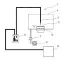
本発明の被膜形成方法を図1に基づいて説明する。図1は平板基材上にセラミックス被膜を形成する場合の被膜形成装置を示す図である。
図1に示すように、AD法による被膜形成装置1は、エアロゾル発生装置3と、真空チャンバー4を有する。真空チャンバー4内には、表面粗さRaが 0.01μm より大きく 0.5μm 未満である金属製基材5と、エアロゾル吐出ノズル2とが配設されている。真空チャンバー4の内部は真空ポンプ6によって減圧されるとともに、セラミックス微粒子の混入を防止するため、真空ポンプ6の直前に微粒子フィルター7が設けられている。基材5は、真空チャンバー4内において、XYテーブル8上に固定され水平方向に移動させられる(図中A)。The film forming method of the present invention will be described with reference to FIG. FIG. 1 is a diagram showing a film forming apparatus in the case of forming a ceramic film on a flat substrate.
As shown in FIG. 1, a film forming apparatus 1 using an AD method includes an aerosol generating device 3 and a
内部にセラミックス微粒子を有するエアロゾル発生装置3は、外部にガス供給設備9を備え、ガス供給設備9から供給される搬送ガスによってセラミックス微粒子と搬送ガスとからなるエアロゾルが形成され、該エアロゾルは搬送ガスの流れと真空ポンプ6の吸引とにより真空チャンバー4内のエアロゾル吐出ノズル2に供給される。エアロゾルの搬送ガスとしては、不活性ガス等を使用する。使用可能な不活性ガスとしては、アルゴン、窒素、ヘリウム等が挙げられる。 The aerosol generating device 3 having ceramic fine particles therein includes a gas supply facility 9 outside, and an aerosol composed of ceramic fine particles and a carrier gas is formed by a carrier gas supplied from the gas supply facility 9, and the aerosol is a carrier gas. And the suction of the
エアロゾル吐出ノズル2は、1本であっても複数本であってもよい。また、エアロゾル吐出ノズル2は、真空チャンバー4内で変位可能に構成してもよい。
エアロゾル吐出ノズル2からエアロゾルを吐出しつつ、基材5をXYテーブル8により水平方向に移動させて、または、エアロゾル吐出ノズル2を移動させて、基材5上に所望の形状・厚さの被膜を形成する。
なお、本発明の被膜形成方法では、基材およびセラミックス微粒子を上述の範囲に限定すればよく、上記各装置構成については、AD法において通常使用される任意の装置・部品等を利用できる。The
While discharging the aerosol from the
In the coating film forming method of the present invention, the base material and the ceramic fine particles may be limited to the above-mentioned ranges, and any device / part or the like that is usually used in the AD method can be used for each device configuration.
表面粗さをパラメータとして表1に示す 6 水準を設定した軸受鋼SUJ2製テスト基板(縦 30 mm×横30 mm、厚み 3 mm )を準備した。
この基板表面にAD法でアルミナ微粒子を用いて、セラミックス被膜を 20 分間形成した。AD法は位置決め用XYテーブルを用いて、6 mm/分で移動するテスト基板に、100 Pa 以下の減圧下で、開口サイズ 10 mm× 1 mm のノズルを通してアルミナ微粒子のエアロゾルを噴射して被膜形成を行なった。
アルミナ微粒子は、大明化学工業社製:タイミクロンTM-DARを用い、平均粒子径 0.12μm で、10 Pa 以下の減圧下、加熱乾燥処理して使用した。なお、搬送ガスには窒素を用い、粒子速度は搬送ガス流量で制御した。
得られた被膜の膜厚を測定し、成膜効率を評価した。成膜効率は、幅 10 mm×長さ 10 mm の面状成膜を実施し、その平均膜厚を成膜にかかった時間で割った値とした。この値が大きくなることは、短時間で厚膜化していて成膜にかかる時間が短縮され成膜効率が向上したことを示している。結果を表1に併記する。A test substrate made of bearing steel SUJ2 (length 30 mm x width 30 mm, thickness 3 mm) with 6 levels shown in Table 1 as the surface roughness was prepared.
A ceramic film was formed on this substrate surface for 20 minutes using alumina fine particles by the AD method. The AD method uses a positioning XY table to form a film by spraying an aerosol of alumina fine particles through a nozzle with an opening size of 10 mm x 1 mm on a test substrate moving at 6 mm / min under a reduced pressure of 100 Pa or less. Was done.
Alumina fine particles were manufactured by Daimei Chemical Industry Co., Ltd .: Tymicron TM-DAR. Nitrogen was used as the carrier gas, and the particle velocity was controlled by the carrier gas flow rate.
The film thickness of the obtained film was measured to evaluate the film formation efficiency. The film formation efficiency was a value obtained by dividing the average film thickness by the time required for the film formation when a planar film formation having a width of 10 mm and a length of 10 mm was performed. An increase in this value indicates that the film thickness is increased in a short time, the time required for film formation is shortened, and the film formation efficiency is improved. The results are also shown in Table 1.

本発明のセラミックス被膜形成方法は、セラミックス被膜を形成する金属製基材の表面粗さをRaで 0.01μm より大きく 0.5μm 未満に調整した上で、微粒子を金属製基材に衝突させてセラミックス被膜を形成するので、成膜速度を向上させることができる。このため量産性が向上し、各種産業機械に用いられる耐熱性、耐摩耗性、耐久性、耐食・耐絶縁性等の要求される各種部材にセラミックス被膜を形成する方法として好適に利用できる。 The method for forming a ceramic film of the present invention comprises adjusting the surface roughness of a metal base material on which the ceramic film is formed to a value greater than 0.01 μm and less than 0.5 μm, and then causing the fine particles to collide with the metal base material. Thus, the film formation rate can be improved. For this reason, mass productivity is improved, and it can be suitably used as a method for forming a ceramic coating on various members required for heat resistance, wear resistance, durability, corrosion resistance, insulation resistance, etc. used in various industrial machines.
1 被膜形成装置
2 エアロゾル吐出ノズル
3 エアロゾル発生装置
4 真空チャンバー
5 基材
6 真空ポンプ
7 微粒子フィルター
8 XYテーブル
9 ガス供給設備DESCRIPTION OF SYMBOLS 1
Claims (3)
Translated fromJapanese前記セラミックス微粒子の平均粒子径が 0.1μm 〜 0.5μm であり、前記金属製基材表面の表面粗さRaが 0.01μm より大きく 0.5μm 未満であることを特徴とする被膜形成方法。A method for forming a film by an aerosol deposition method in which ceramic fine particles are dispersed in a gas to form an aerosol, and the aerosol is sprayed onto a metal substrate surface to collide with the film.
An average particle size of the ceramic fine particles is 0.1 μm to 0.5 μm, and a surface roughness Ra of the surface of the metal substrate is more than 0.01 μm and less than 0.5 μm.
Priority Applications (1)
| Application Number | Priority Date | Filing Date | Title |
|---|---|---|---|
| JP2006294167AJP2008111154A (en) | 2006-10-30 | 2006-10-30 | Method for forming coating film |
Applications Claiming Priority (1)
| Application Number | Priority Date | Filing Date | Title |
|---|---|---|---|
| JP2006294167AJP2008111154A (en) | 2006-10-30 | 2006-10-30 | Method for forming coating film |
Publications (1)
| Publication Number | Publication Date |
|---|---|
| JP2008111154Atrue JP2008111154A (en) | 2008-05-15 |
Family
ID=39443833
Family Applications (1)
| Application Number | Title | Priority Date | Filing Date |
|---|---|---|---|
| JP2006294167APendingJP2008111154A (en) | 2006-10-30 | 2006-10-30 | Method for forming coating film |
Country Status (1)
| Country | Link |
|---|---|
| JP (1) | JP2008111154A (en) |
Cited By (5)
| Publication number | Priority date | Publication date | Assignee | Title |
|---|---|---|---|---|
| WO2020017671A1 (en)* | 2018-07-17 | 2020-01-23 | (주)코미코 | Aerosol deposition coating method for plasma-resistant coating |
| US10889900B2 (en) | 2016-03-01 | 2021-01-12 | Nippon Steel Corporation | Ceramic laminate |
| TWI733815B (en)* | 2017-05-25 | 2021-07-21 | 南韓商Komico有限公司 | Method of aerosol deposition coating for plasma resistant coating |
| WO2022211114A1 (en) | 2021-04-02 | 2022-10-06 | 豊実精工株式会社 | Ceramic coating member |
| US12414429B2 (en) | 2020-05-19 | 2025-09-09 | Ricoh Company, Ltd. | Metal oxide particles having p-type semiconductivity, electronic device using the same, method for manufacturing electronic device, and image forming apparatus |
- 2006
- 2006-10-30JPJP2006294167Apatent/JP2008111154A/enactivePending
Cited By (8)
| Publication number | Priority date | Publication date | Assignee | Title |
|---|---|---|---|---|
| US10889900B2 (en) | 2016-03-01 | 2021-01-12 | Nippon Steel Corporation | Ceramic laminate |
| TWI733815B (en)* | 2017-05-25 | 2021-07-21 | 南韓商Komico有限公司 | Method of aerosol deposition coating for plasma resistant coating |
| WO2020017671A1 (en)* | 2018-07-17 | 2020-01-23 | (주)코미코 | Aerosol deposition coating method for plasma-resistant coating |
| CN111164237A (en)* | 2018-07-17 | 2020-05-15 | Komico有限公司 | Aerogel Deposition Coating Method for Plasma Resistant Coatings |
| US11795547B2 (en)* | 2018-07-17 | 2023-10-24 | Komico Ltd. | Method of aerosol deposition coating for plasma resistant coating |
| US12414429B2 (en) | 2020-05-19 | 2025-09-09 | Ricoh Company, Ltd. | Metal oxide particles having p-type semiconductivity, electronic device using the same, method for manufacturing electronic device, and image forming apparatus |
| WO2022211114A1 (en) | 2021-04-02 | 2022-10-06 | 豊実精工株式会社 | Ceramic coating member |
| KR20230164164A (en) | 2021-04-02 | 2023-12-01 | 호지츠 세이코 가부시키가이샤 | No ceramic coating |
Similar Documents
| Publication | Publication Date | Title |
|---|---|---|
| CN101168842B (en) | Low temperature aerosol deposition of a plasma resistive layer | |
| JP6117195B2 (en) | Parts for plasma processing apparatus and method for manufacturing parts for plasma processing apparatus | |
| KR100966132B1 (en) | Ceramic coating having plasma resistance | |
| KR101110371B1 (en) | Plasma-resistant crystalline ceramic coating film and its manufacturing method | |
| JP6084464B2 (en) | Plasma etching apparatus component and method for manufacturing plasma etching apparatus component | |
| KR102499540B1 (en) | Member for semiconductor manufacturing device and semiconductor manufacturing device with member for semiconductor manufacturing device and display manufacturing device | |
| EP3382059B1 (en) | Method for producing laminate | |
| JP2005158933A (en) | Semiconductor or liquid crystal manufacturing apparatus member and manufacturing method thereof | |
| JP5605901B2 (en) | Method for repairing metal material by cold spray method, method for producing powder material for cold spray, and cold spray film | |
| JP2008111154A (en) | Method for forming coating film | |
| JP2008081775A (en) | Method for forming alumina coating film | |
| JPWO2010027073A1 (en) | Semiconductor manufacturing equipment parts and semiconductor manufacturing equipment | |
| KR102612460B1 (en) | Member for semiconductor manufacturing apparatus and semiconductor manufacturing apparatus | |
| KR20100011586A (en) | Method of forming ceramic coating layer having the resistant plasma | |
| JP2007320797A (en) | Composite structure and its manufacturing method | |
| US9481922B2 (en) | Process for forming porous metal coating on surfaces | |
| JP3897623B2 (en) | Composite structure manufacturing method | |
| KR101573010B1 (en) | MANUFACTURING METHOD AND APPARATUS OF SiC COATING LAYERS | |
| JP2008056948A (en) | Pretreatment method for ceramic fine particle | |
| KR102084841B1 (en) | Surface treating method for controlling surface roughness of carbon material | |
| JP2009132945A (en) | Method for forming film-formed body by aerosol deposition process | |
| JP2008069399A (en) | Film deposition method | |
| JP2008029977A (en) | Aerosol discharge nozzle and coating-film forming device | |
| JP2007246943A (en) | Method for making body having formed from brittle material by aerosol deposition method | |
| JP2014208881A (en) | Composite structure |