JP2008109043A - Semiconductor device manufacturing method and semiconductor device - Google Patents
Semiconductor device manufacturing method and semiconductor deviceDownload PDFInfo
- Publication number
- JP2008109043A JP2008109043AJP2006292782AJP2006292782AJP2008109043AJP 2008109043 AJP2008109043 AJP 2008109043AJP 2006292782 AJP2006292782 AJP 2006292782AJP 2006292782 AJP2006292782 AJP 2006292782AJP 2008109043 AJP2008109043 AJP 2008109043A
- Authority
- JP
- Japan
- Prior art keywords
- insulating film
- semiconductor device
- wiring
- wirings
- semiconductor
- Prior art date
- Legal status (The legal status is an assumption and is not a legal conclusion. Google has not performed a legal analysis and makes no representation as to the accuracy of the status listed.)
- Pending
Links
- 239000004065semiconductorSubstances0.000titleclaimsabstractdescription67
- 238000004519manufacturing processMethods0.000titleclaimsabstractdescription14
- 239000000758substrateSubstances0.000claimsabstractdescription21
- 238000005268plasma chemical vapour depositionMethods0.000claimsabstractdescription20
- 230000002093peripheral effectEffects0.000claimsdescription16
- VYPSYNLAJGMNEJ-UHFFFAOYSA-NSilicium dioxideChemical compoundO=[Si]=OVYPSYNLAJGMNEJ-UHFFFAOYSA-N0.000claimsdescription10
- 229910052814silicon oxideInorganic materials0.000claimsdescription10
- 238000000034methodMethods0.000claimsdescription7
- 229910052581Si3N4Inorganic materials0.000claimsdescription5
- 238000005229chemical vapour depositionMethods0.000claimsdescription5
- HQVNEWCFYHHQES-UHFFFAOYSA-Nsilicon nitrideChemical compoundN12[Si]34N5[Si]62N3[Si]51N64HQVNEWCFYHHQES-UHFFFAOYSA-N0.000claimsdescription5
- 239000010410layerSubstances0.000description13
- 230000015572biosynthetic processEffects0.000description5
- NRTOMJZYCJJWKI-UHFFFAOYSA-NTitanium nitrideChemical compound[Ti]#NNRTOMJZYCJJWKI-UHFFFAOYSA-N0.000description2
- 229910016570AlCuInorganic materials0.000description1
- 229910004298SiO 2Inorganic materials0.000description1
- BLRPTPMANUNPDV-UHFFFAOYSA-NSilaneChemical compound[SiH4]BLRPTPMANUNPDV-UHFFFAOYSA-N0.000description1
- XUIMIQQOPSSXEZ-UHFFFAOYSA-NSiliconChemical compound[Si]XUIMIQQOPSSXEZ-UHFFFAOYSA-N0.000description1
- BOTDANWDWHJENH-UHFFFAOYSA-NTetraethyl orthosilicateChemical compoundCCO[Si](OCC)(OCC)OCCBOTDANWDWHJENH-UHFFFAOYSA-N0.000description1
- WPPDFTBPZNZZRP-UHFFFAOYSA-Naluminum copperChemical compound[Al].[Cu]WPPDFTBPZNZZRP-UHFFFAOYSA-N0.000description1
- 238000005520cutting processMethods0.000description1
- 238000000151depositionMethods0.000description1
- 230000008021depositionEffects0.000description1
- 230000000994depressogenic effectEffects0.000description1
- 238000010586diagramMethods0.000description1
- 230000000694effectsEffects0.000description1
- 238000009413insulationMethods0.000description1
- 239000011229interlayerSubstances0.000description1
- 238000010030laminatingMethods0.000description1
- 229910052751metalInorganic materials0.000description1
- 239000002184metalSubstances0.000description1
- 238000002161passivationMethods0.000description1
- 238000000059patterningMethods0.000description1
- 229910052710siliconInorganic materials0.000description1
- 239000010703siliconSubstances0.000description1
- 238000004544sputter depositionMethods0.000description1
Images


Classifications
- H—ELECTRICITY
- H01—ELECTRIC ELEMENTS
- H01L—SEMICONDUCTOR DEVICES NOT COVERED BY CLASS H10
- H01L21/00—Processes or apparatus adapted for the manufacture or treatment of semiconductor or solid state devices or of parts thereof
- H01L21/70—Manufacture or treatment of devices consisting of a plurality of solid state components formed in or on a common substrate or of parts thereof; Manufacture of integrated circuit devices or of parts thereof
- H01L21/71—Manufacture of specific parts of devices defined in group H01L21/70
- H01L21/768—Applying interconnections to be used for carrying current between separate components within a device comprising conductors and dielectrics
- H01L21/76801—Applying interconnections to be used for carrying current between separate components within a device comprising conductors and dielectrics characterised by the formation and the after-treatment of the dielectrics, e.g. smoothing
- H01L21/7682—Applying interconnections to be used for carrying current between separate components within a device comprising conductors and dielectrics characterised by the formation and the after-treatment of the dielectrics, e.g. smoothing the dielectric comprising air gaps
- H—ELECTRICITY
- H01—ELECTRIC ELEMENTS
- H01L—SEMICONDUCTOR DEVICES NOT COVERED BY CLASS H10
- H01L21/00—Processes or apparatus adapted for the manufacture or treatment of semiconductor or solid state devices or of parts thereof
- H01L21/70—Manufacture or treatment of devices consisting of a plurality of solid state components formed in or on a common substrate or of parts thereof; Manufacture of integrated circuit devices or of parts thereof
- H01L21/71—Manufacture of specific parts of devices defined in group H01L21/70
- H01L21/768—Applying interconnections to be used for carrying current between separate components within a device comprising conductors and dielectrics
- H01L21/76801—Applying interconnections to be used for carrying current between separate components within a device comprising conductors and dielectrics characterised by the formation and the after-treatment of the dielectrics, e.g. smoothing
Landscapes
- Engineering & Computer Science (AREA)
- Physics & Mathematics (AREA)
- Condensed Matter Physics & Semiconductors (AREA)
- General Physics & Mathematics (AREA)
- Manufacturing & Machinery (AREA)
- Computer Hardware Design (AREA)
- Microelectronics & Electronic Packaging (AREA)
- Power Engineering (AREA)
- Internal Circuitry In Semiconductor Integrated Circuit Devices (AREA)
Abstract
Description
Translated fromJapanese本願発明は、半導体装置の製造方法に関するものであり、特に、半導体基板上に形成された配線の配線間にエアーギャップが形成されている半導体装置の製造方法に関するものである。The present invention relates to a method for manufacturing a semiconductor device, and more particularly, to a method for manufacturing a semiconductor device in which an air gap is formed between wirings formed on a semiconductor substrate.
従来、半導体基板上に形成された配線の配線間の容量を低減させることを目的として、この配線間にエアーギャップを備える半導体装置が知られている。 2. Description of the Related Art Conventionally, a semiconductor device having an air gap between wirings is known for the purpose of reducing the capacitance between wirings formed on a semiconductor substrate.
このエアーギャップを備える半導体装置の製造方法は、半導体基板上に形成された第1の絶縁膜上に互いに隣接するように配線を形成する工程と、この第1の絶縁膜上にプラズマCVD法により第2の絶縁膜を形成して隣接する配線の配線間にエアーギャップが形成されるように配線を第2の絶縁膜により覆う工程と、この第2の絶縁膜上に耐湿性の高い第3の絶縁膜を形成する工程とを有している。
このような構成は例えば特許文献1で開示されている。A method of manufacturing a semiconductor device having the air gap includes a step of forming wirings on a first insulating film formed on a semiconductor substrate so as to be adjacent to each other, and a plasma CVD method on the first insulating film. Forming a second insulating film and covering the wiring with a second insulating film so that an air gap is formed between adjacent wirings; and a third layer having high moisture resistance on the second insulating film. Forming an insulating film.
Such a configuration is disclosed in Patent Document 1, for example.
特許文献1では、図1および段落0011〜0014に示されているように、半導体基板201上に形成された絶縁膜202上に、互いに隣接するように最上層配線203を形成し、絶縁膜202上にプラズマCVD法によりシリコン酸化膜204を形成して隣接する最上層配線203の配線間に空洞部207が形成されるように最上層配線203を覆い、さらに、シリコン酸化膜204上に最終保護膜となるシリコン窒化膜205を形成することについて開示されている。 In Patent Document 1, as shown in FIG. 1 and paragraphs 0011 to 0014, an uppermost layer wiring 203 is formed on an insulating film 202 formed on a semiconductor substrate 201 so as to be adjacent to each other. A silicon oxide film 204 is formed thereon by plasma CVD to cover the uppermost layer wiring 203 so that a cavity 207 is formed between adjacent uppermost layer wirings 203, and further, a final protection is provided on the silicon oxide film 204. It is disclosed that a silicon nitride film 205 to be a film is formed.
しかしながら、上述した従来の構成では、エアーギャップを形成する絶縁膜が段差被覆性の低いプラズマCVD法により形成されているため、絶縁膜の表面の平坦性が良好ではない。このためこの絶縁膜上に形成される耐湿性の高い絶縁膜の被覆性が低減してしまう可能性があり、これにより、半導体装置の耐湿性が低減してしまう可能性があった。However, in the conventional configuration described above, since the insulating film forming the air gap is formed by the plasma CVD method having a low step coverage, the flatness of the surface of the insulating film is not good. For this reason, there is a possibility that the coverage of the highly moisture-resistant insulating film formed on this insulating film may be reduced, and this may reduce the moisture resistance of the semiconductor device.
上記課題を解決する為、本願発明の半導体装置の製造方法では、半導体基板上に形成された第1の絶縁膜上に、互いに隣接するように複数の配線を形成する工程と、第1の絶縁膜上にプラズマCVD法により第2の絶縁膜を形成して、隣接する配線の配線間にエアーギャップが形成されるように配線を第2の絶縁膜により覆う工程と、第2の絶縁膜上に高密度プラズマCVD法により、第3の絶縁膜を形成する工程と、第3の絶縁膜上に、第2および第3の絶縁膜よりも耐湿性の高い第4の絶縁膜を形成する工程とを有する。In order to solve the above problems, in the method of manufacturing a semiconductor device of the present invention, a step of forming a plurality of wirings adjacent to each other on a first insulating film formed on a semiconductor substrate, and a first insulation Forming a second insulating film on the film by plasma CVD and covering the wiring with the second insulating film so that an air gap is formed between the wirings of adjacent wirings; Forming a third insulating film by high-density plasma CVD, and forming a fourth insulating film having higher moisture resistance than the second and third insulating films on the third insulating film. And have.
この構成によれば、エアーギャップを形成する絶縁膜上に形成される耐湿性の高い絶縁膜の被覆性を向上させることが可能となり、半導体装置の耐湿性を向上させることが可能となる。According to this configuration, it is possible to improve the coverage of the highly moisture-resistant insulating film formed on the insulating film that forms the air gap, and it is possible to improve the moisture resistance of the semiconductor device.
以下、本願発明の実施例について図面を参照して詳細に説明する。なお、全図面を通して同様の構成には同様の符号を付与する。Hereinafter, embodiments of the present invention will be described in detail with reference to the drawings. In addition, the same code | symbol is provided to the same structure through all the drawings.
図1〜図7は、本願発明の実施例1における半導体装置の製造方法を説明する工程図である。ここで、図1〜図6は半導体装置の断面図である。1 to 7 are process diagrams for explaining a method of manufacturing a semiconductor device according to the first embodiment of the present invention. 1 to 6 are cross-sectional views of the semiconductor device.
本願発明の実施例1では、図1に示されるように、半導体基板100上に形成された第1の絶縁膜200上に、互いに隣接するように複数の配線300を形成する。 In the first embodiment of the present invention, as shown in FIG. 1, a plurality of
半導体基板100はシリコン(Si)基板である。第1の絶縁膜200はシリコン酸化(SiO2)膜であり、高密度プラズマCVD(High Density Plasma Chemical Vapor Deposition)法で形成される。配線300は、窒化チタン(TiN)膜、アルミ銅(AlCu)膜、窒化チタン(TiN)膜が順次積層された積層構造を備える。配線300は、上記の各金属膜をスパッタリング法により積層し、これをパターニングすることで得られる。 The
本実施例では、配線120は、図6に示されるように、半導体基板100上に形成された多層配線層400の最上層に形成された配線に相当する。 In this embodiment, the
つまり、本実施例では、トランジスタ等の電子素子が形成された半導体基板100上に層間絶縁膜210と配線310とが順次積層された多層配線層400が形成されており、第1の絶縁膜200は多層配線層400の最上層の絶縁膜210に相当し、配線300は多層配線層400の最上層の配線310に相当する。なお、多層配線層400の最上層には外部と電気的に接続される電極パッド320が形成されている。
さらに、本実施例の半導体装置は半導体記憶装置に関するものでありメモリセル101とメモリセル101からデータを読み出すビット線とを備える。That is, in this embodiment, the
Further, the semiconductor device of this embodiment relates to a semiconductor memory device, and includes a
本実施例では、半導体基板100は、メモリセル101が形成されるメモリセル領域110と、周辺トランジスタ102が形成される周辺領域120とに区別されている。メモリセル領域110上に配置される配線300は、メモリセル101からデータの読出しを行なうビット線に対応する。周辺領域120上に配置される配線300はその他の配線300である。 In this embodiment, the
メモリセル領域110上および周辺領域120上に配置される配線300は、図1に示されるように、隣接する配線と所定間隔離間して配置され、図1の奥行き方向に延在している。 As shown in FIG. 1, the
メモリセル領域110に配置される配線300は、配線間隔が周辺領域120上に配置された配線300よりも狭くなるように配置されている。
本実施例では、メモリセル領域110上に配置される配線300の配線幅wは0.376μmで、配線間隔dは0.264μmであり、周辺領域120上に配置される配線300の配線幅w´は0.80μmで、配線間隔d´は0.80μmである。
次に、図2に示されているように、第1の絶縁膜200上にプラズマCVD(Plasma Chemical Vapor Deposition)法により第2の絶縁膜500を形成して、隣接する配線300の配線間にエアーギャップ510が形成されるように配線300を第2の絶縁膜500により覆う。The
In the present embodiment, the wiring width w of the
Next, as shown in FIG. 2, a second
本実施例では、第2の絶縁膜500はシリコン酸化膜である。第2の絶縁膜500の膜厚は4000Åである。プラズマCVD法による第2の絶縁膜の成膜は、TEOS流量:100sccm、O2流量:1.6SLM、圧力:3.0Torr、高周波パワー:450W、低周波パワー:300、成膜温度:420℃の条件で行なわれる。 In this embodiment, the second
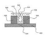
図5に示されるように、プラズマCVD法による成膜では、配線間の上部530における成膜が他の箇所よりも先に進み、配線間を十分に埋め込む前に、配線間の上部530が塞がる。これにより、配線間の狭い箇所では配線間にエアーギャップ510が形成される。なお、図5は、図2におけるメモリセル領域110上に配置された配線300の拡大図に相当する。 As shown in FIG. 5, in the film formation by the plasma CVD method, the film formation in the
さらに詳しく説明すると、配線300の配線間において、中央から上方に渡りエアーギャップ510が形成されており、配線間の下部520と上部530は第2の絶縁膜500により埋め込まれている。配線300の側面は第2の絶縁膜500により覆われている。エアーギャップ510の上端は配線300の上端よりも高いレベルに位置する。 More specifically, an
ここで、第2の絶縁膜500の成膜は、隣り合う各配線300から互いに向かい合うように進むため、それらが交わる箇所において溝540が形成される。つまり、エアーギャップ510の上方に位置する第2の絶縁膜500の表面には、溝540が形成される。
さらに、プラズマCVD法による埋め込み性は、配線の間隔に対する配線の高さの比であるアスペクト比に依存し、配線300のうち配線間隔が狭い箇所でありアスペクト比が大きい箇所では、上述したように配線間が十分に第2の絶縁膜500で埋め込まれずに配線間にエアーギャップ510が形成される一方、配線間隔が広い箇所でありアスペクト比が高い箇所では、配線間が十分に第2の絶縁膜500で埋め込まれ、エアーギャップ510は形成されない。Here, since the film formation of the second
Further, the embedding property by the plasma CVD method depends on the aspect ratio that is the ratio of the height of the wiring to the wiring spacing, and in the
本実施例では、図2に示されるように、メモリセル領域110上に配置される配線300の配線間にはエアーギャップ510が形成され、周辺領域120上に配置される配線300の配線間は第2の絶縁膜500で十分に埋め込まれてエアーギャップ510は形成されない。本実施例では、メモリセル領域110上に配置される配線300のアスペクト比は2以上であり、周辺領域120上に配置される配線300のアスペクト比は2よりも小さい。 In this embodiment, as shown in FIG. 2, an
ここで、周辺領域120上において第2の絶縁膜500は配線間で窪むようにして形成されるため、第2の絶縁膜500の配線300と配線間との境界では段差550が形成される。 Here, since the second
このように、本願発明では、半導体基板上に形成された配線300は、互いにエアーギャップ510を挟んで配置されるため、配線間容量を低減することが可能となる。
つまり、エアーギャップ510は第2の絶縁膜500に比べて誘電率が低い為、配線間にエアーギャップ510を設けることで、配線間が全て第2の絶縁膜500で埋め込まれている構成と比べて、大幅に配線間容量を低減することが可能となる。これにより、配線300を伝達する信号の速度を大幅に向上させることが可能となる。As described above, according to the present invention, since the
That is, since the
特に、本実施例では、このエアーギャップ510が間に形成される配線300が、メモリセル101からデータを読み出すためのビット線に相当するため、高速化が特に求められているデータの読出し速度を大幅に向上させることが可能となる。これにより、デバイスとしての特性を大幅に向上させることが可能となり、本願発明を適用することの効果をより顕著に得ることが可能となる。 In particular, in this embodiment, since the
また、本実施例では、エアーギャップを形成する第2の絶縁膜500の膜厚は上述したように4000Åであるが、発明者の研究によると、第2の絶縁膜500の膜厚が3000Å以上であれば、配線間容量を十分に低減することが可能なエアーギャップ510が形成されることが明らかとなっている。 In this embodiment, the thickness of the second
さらに、本実施例では、上述したように、エアーギャップ510の上端は配線300の上端よりも高いレベルに位置しているため、配線間容量をより十分に低減させることが可能となる。 Further, in the present embodiment, as described above, the upper end of the
次に、図3に示されるように、第2の絶縁膜500上に、高密度プラズマCVD(High Density Plasma Chemical Vapor Deposition)法により、第3の絶縁膜600を形成する。 Next, as shown in FIG. 3, a third
本実施例では、第3の絶縁膜600はシリコン酸化膜である。第3の絶縁膜の膜厚は8000Åである。高密度プラズマCVD法による第3の絶縁膜600の成膜は、SiH4流量:120sccm、O2流量:170sccm、Ar流量:240sccm、低周波パワー:4200W、高周波パワー:2950W、He圧力:7.0の条件で行なわれる。
高密度プラズマCVD法による成膜では、堆積膜を削りながら成膜が行なわれるため、下地層に段差がある場合でも、平坦性の高い膜を成膜することが可能となる。In this embodiment, the third
In film formation by the high-density plasma CVD method, film formation is performed while cutting the deposited film, so that a film with high flatness can be formed even when there is a step in the base layer.
つまり、この構成によれば、エアーギャップ510の上方に位置する第2の絶縁膜500の表面に形成された溝540は、第3の絶縁膜600により埋め込まれて、この溝540上には平坦性の高い第3の絶縁膜600が成膜される。すなわち、メモリセル領域110上において、平坦性の高い表面を得ることが可能となる。 In other words, according to this configuration, the
さらに、この構成によれば、周辺領域120上における第2の絶縁膜500に形成された段差550上において、なだらかな形状となるように第3の絶縁膜600が形成されるため、周辺領域120上においても、平坦性の高い表面を得ることが可能となる。
次に、第3の絶縁膜600上に、第2の絶縁膜500および第3の絶縁膜600よりも耐湿性の高い第4の絶縁膜700を形成する。Furthermore, according to this configuration, the third
Next, the second
第4の絶縁膜700は、外部から水分が浸入することを防止するための耐湿性の高いパッシベーション膜であり、本実施例では、第4の絶縁膜700は、シリコン窒化(SiN)膜である。第4の絶縁膜700は、プラズマCVD法により成膜される。第4の絶縁膜700の膜厚は3000Åである。なお、第4の絶縁膜700は、電極パッド320を露出するように形成される。 The fourth
本願発明では、第4の絶縁膜700は上述したように平坦性の高い表面を備える第3の絶縁膜600上に成膜されるため、成膜される第4の絶縁膜700の被覆性は高上する。
これにより、外部からの水分等の浸入を第4の絶縁膜700で十分に防ぐことが可能となり、半導体装置の耐湿性を向上させることが可能となる。
さらに、本実施例では、第4の絶縁膜700上に、第5の絶縁膜800が形成されている。In the present invention, since the fourth insulating
Thus, the fourth insulating
Further, in this embodiment, a fifth
第5の絶縁膜800はシリコン酸化膜であり、プラズマCVD法によって成膜される。第5の絶縁膜800の膜厚は6000Åである。なお、第5の絶縁膜800は、電極パッド320を露出するように形成される。 The fifth
100 半導体基板
101 メモリセル
102 周辺トランジスタ
110 メモリセル領域
120 周辺領域
200,210 第1の絶縁膜
300,310 配線
320 電極パッド
400 多層配線層
500 第2の絶縁膜
510 エアーギャップ
600 第3の絶縁膜
700 第4の絶縁膜
800 第5の絶縁膜100
Claims (16)
Translated fromJapanese前記第1の絶縁膜上にプラズマCVD法により第2の絶縁膜を形成して、前記隣接する配線の配線間にエアーギャップが形成されるように前記配線を前記第2の絶縁膜により覆う工程と、
前記第2の絶縁膜上に高密度プラズマCVD法により、第3の絶縁膜を形成する工程と、
前記第3の絶縁膜上に、前記第2および前記第3の絶縁膜よりも耐湿性の高い第4の絶縁膜を形成する工程とを有することを特徴とする半導体装置の製造方法。Forming a plurality of wirings adjacent to each other on the first insulating film formed on the semiconductor substrate;
Forming a second insulating film on the first insulating film by a plasma CVD method, and covering the wiring with the second insulating film so that an air gap is formed between the wirings of the adjacent wirings; When,
Forming a third insulating film on the second insulating film by high-density plasma CVD;
Forming a fourth insulating film having higher moisture resistance than the second and third insulating films on the third insulating film.
前記配線は、前記ビット線に対応することを特徴とする請求項1〜6のいずれか1つに記載の半導体装置の製造方法。The semiconductor device is a semiconductor memory device, and the semiconductor device includes a memory cell and a bit line for reading data from the memory cell,
The method of manufacturing a semiconductor device according to claim 1, wherein the wiring corresponds to the bit line.
前記メモリセル領域上に配置される前記隣接する配線の配線間に、前記エアーギャップが形成されることを特徴とする請求項1〜6のいずれか1つに記載の半導体装置の製造方法。The semiconductor device is a semiconductor memory device, and the semiconductor substrate includes a memory cell region in which a memory cell is formed and a peripheral region in which a peripheral transistor is formed,
7. The method of manufacturing a semiconductor device according to claim 1, wherein the air gap is formed between the adjacent wirings arranged on the memory cell region.
前記半導体基板上に形成された第1の絶縁膜と、
前記第1の絶縁膜上に互いに隣接するように形成された複数の配線と、
前記第1の絶縁膜上にCVD法により形成され、前記隣接する配線の配線間にエアーギャップが形成されるように前記配線を覆う第2の絶縁膜と、
前記第2の絶縁膜上に高密度プラズマCVD法により形成された第3の絶縁膜と、
前記第3の絶縁膜上に形成され、前記第2および前記第3の絶縁膜よりも耐湿性の高い第4の絶縁膜と、
を有することを特徴とする半導体装置。A semiconductor substrate;
A first insulating film formed on the semiconductor substrate;
A plurality of wirings formed on the first insulating film so as to be adjacent to each other;
A second insulating film formed on the first insulating film by a CVD method and covering the wiring so that an air gap is formed between the wirings of the adjacent wirings;
A third insulating film formed on the second insulating film by a high-density plasma CVD method;
A fourth insulating film formed on the third insulating film and having higher moisture resistance than the second and third insulating films;
A semiconductor device comprising:
前記配線は、前記ビット線に対応することを特徴とする請求項9〜14のいずれか1つに記載の半導体装置。The semiconductor device is a semiconductor memory device, and the semiconductor device includes a memory cell and a bit line for reading data from the memory cell,
The semiconductor device according to claim 9, wherein the wiring corresponds to the bit line.
前記メモリセル領域上に配置される前記隣接する配線の配線間に、前記エアーギャップが形成されることを特徴とする請求項9〜14のいずれか1つに記載の半導体装置。The semiconductor device is a semiconductor memory device, and the semiconductor substrate includes a memory cell region in which a memory cell is formed and a peripheral region in which a peripheral transistor is formed,
The semiconductor device according to claim 9, wherein the air gap is formed between the adjacent wirings arranged on the memory cell region.
Priority Applications (2)
| Application Number | Priority Date | Filing Date | Title |
|---|---|---|---|
| JP2006292782AJP2008109043A (en) | 2006-10-27 | 2006-10-27 | Semiconductor device manufacturing method and semiconductor device |
| US11/905,918US7867890B2 (en) | 2006-10-27 | 2007-10-05 | Manufacturing method of semiconductor device and semiconductor device |
Applications Claiming Priority (1)
| Application Number | Priority Date | Filing Date | Title |
|---|---|---|---|
| JP2006292782AJP2008109043A (en) | 2006-10-27 | 2006-10-27 | Semiconductor device manufacturing method and semiconductor device |
Publications (1)
| Publication Number | Publication Date |
|---|---|
| JP2008109043Atrue JP2008109043A (en) | 2008-05-08 |
Family
ID=39329125
Family Applications (1)
| Application Number | Title | Priority Date | Filing Date |
|---|---|---|---|
| JP2006292782APendingJP2008109043A (en) | 2006-10-27 | 2006-10-27 | Semiconductor device manufacturing method and semiconductor device |
Country Status (2)
| Country | Link |
|---|---|
| US (1) | US7867890B2 (en) |
| JP (1) | JP2008109043A (en) |
Cited By (1)
| Publication number | Priority date | Publication date | Assignee | Title |
|---|---|---|---|---|
| JP2011181898A (en)* | 2010-02-04 | 2011-09-15 | Tokyo Ohka Kogyo Co Ltd | Silica-based film forming material for formation of air gap, and method for forming air gap |
Families Citing this family (132)
| Publication number | Priority date | Publication date | Assignee | Title |
|---|---|---|---|---|
| JP4703669B2 (en)* | 2008-02-18 | 2011-06-15 | 株式会社東芝 | Semiconductor memory device and manufacturing method thereof |
| US9324576B2 (en) | 2010-05-27 | 2016-04-26 | Applied Materials, Inc. | Selective etch for silicon films |
| US10283321B2 (en) | 2011-01-18 | 2019-05-07 | Applied Materials, Inc. | Semiconductor processing system and methods using capacitively coupled plasma |
| US8999856B2 (en) | 2011-03-14 | 2015-04-07 | Applied Materials, Inc. | Methods for etch of sin films |
| US9064815B2 (en) | 2011-03-14 | 2015-06-23 | Applied Materials, Inc. | Methods for etch of metal and metal-oxide films |
| JP2012199277A (en)* | 2011-03-18 | 2012-10-18 | Toshiba Corp | Method for manufacturing electronic components |
| US8808563B2 (en) | 2011-10-07 | 2014-08-19 | Applied Materials, Inc. | Selective etch of silicon by way of metastable hydrogen termination |
| US9267739B2 (en) | 2012-07-18 | 2016-02-23 | Applied Materials, Inc. | Pedestal with multi-zone temperature control and multiple purge capabilities |
| US9373517B2 (en) | 2012-08-02 | 2016-06-21 | Applied Materials, Inc. | Semiconductor processing with DC assisted RF power for improved control |
| US9034770B2 (en) | 2012-09-17 | 2015-05-19 | Applied Materials, Inc. | Differential silicon oxide etch |
| US9023734B2 (en) | 2012-09-18 | 2015-05-05 | Applied Materials, Inc. | Radical-component oxide etch |
| US9390937B2 (en) | 2012-09-20 | 2016-07-12 | Applied Materials, Inc. | Silicon-carbon-nitride selective etch |
| US9132436B2 (en) | 2012-09-21 | 2015-09-15 | Applied Materials, Inc. | Chemical control features in wafer process equipment |
| US8969212B2 (en) | 2012-11-20 | 2015-03-03 | Applied Materials, Inc. | Dry-etch selectivity |
| US8980763B2 (en) | 2012-11-30 | 2015-03-17 | Applied Materials, Inc. | Dry-etch for selective tungsten removal |
| US9111877B2 (en) | 2012-12-18 | 2015-08-18 | Applied Materials, Inc. | Non-local plasma oxide etch |
| US8921234B2 (en) | 2012-12-21 | 2014-12-30 | Applied Materials, Inc. | Selective titanium nitride etching |
| US10256079B2 (en) | 2013-02-08 | 2019-04-09 | Applied Materials, Inc. | Semiconductor processing systems having multiple plasma configurations |
| US9362130B2 (en) | 2013-03-01 | 2016-06-07 | Applied Materials, Inc. | Enhanced etching processes using remote plasma sources |
| US9040422B2 (en) | 2013-03-05 | 2015-05-26 | Applied Materials, Inc. | Selective titanium nitride removal |
| US20140271097A1 (en) | 2013-03-15 | 2014-09-18 | Applied Materials, Inc. | Processing systems and methods for halide scavenging |
| US9493879B2 (en) | 2013-07-12 | 2016-11-15 | Applied Materials, Inc. | Selective sputtering for pattern transfer |
| US9773648B2 (en) | 2013-08-30 | 2017-09-26 | Applied Materials, Inc. | Dual discharge modes operation for remote plasma |
| US9576809B2 (en) | 2013-11-04 | 2017-02-21 | Applied Materials, Inc. | Etch suppression with germanium |
| US9520303B2 (en) | 2013-11-12 | 2016-12-13 | Applied Materials, Inc. | Aluminum selective etch |
| US9245762B2 (en) | 2013-12-02 | 2016-01-26 | Applied Materials, Inc. | Procedure for etch rate consistency |
| US9287095B2 (en) | 2013-12-17 | 2016-03-15 | Applied Materials, Inc. | Semiconductor system assemblies and methods of operation |
| US9287134B2 (en) | 2014-01-17 | 2016-03-15 | Applied Materials, Inc. | Titanium oxide etch |
| US9293568B2 (en) | 2014-01-27 | 2016-03-22 | Applied Materials, Inc. | Method of fin patterning |
| US9396989B2 (en) | 2014-01-27 | 2016-07-19 | Applied Materials, Inc. | Air gaps between copper lines |
| US9385028B2 (en) | 2014-02-03 | 2016-07-05 | Applied Materials, Inc. | Air gap process |
| US9499898B2 (en) | 2014-03-03 | 2016-11-22 | Applied Materials, Inc. | Layered thin film heater and method of fabrication |
| US9299575B2 (en) | 2014-03-17 | 2016-03-29 | Applied Materials, Inc. | Gas-phase tungsten etch |
| US9299537B2 (en) | 2014-03-20 | 2016-03-29 | Applied Materials, Inc. | Radial waveguide systems and methods for post-match control of microwaves |
| US9903020B2 (en) | 2014-03-31 | 2018-02-27 | Applied Materials, Inc. | Generation of compact alumina passivation layers on aluminum plasma equipment components |
| US9269590B2 (en) | 2014-04-07 | 2016-02-23 | Applied Materials, Inc. | Spacer formation |
| US9309598B2 (en) | 2014-05-28 | 2016-04-12 | Applied Materials, Inc. | Oxide and metal removal |
| US9406523B2 (en) | 2014-06-19 | 2016-08-02 | Applied Materials, Inc. | Highly selective doped oxide removal method |
| US9378969B2 (en) | 2014-06-19 | 2016-06-28 | Applied Materials, Inc. | Low temperature gas-phase carbon removal |
| US9425058B2 (en) | 2014-07-24 | 2016-08-23 | Applied Materials, Inc. | Simplified litho-etch-litho-etch process |
| US9378978B2 (en) | 2014-07-31 | 2016-06-28 | Applied Materials, Inc. | Integrated oxide recess and floating gate fin trimming |
| US9159606B1 (en)* | 2014-07-31 | 2015-10-13 | Applied Materials, Inc. | Metal air gap |
| US9496167B2 (en) | 2014-07-31 | 2016-11-15 | Applied Materials, Inc. | Integrated bit-line airgap formation and gate stack post clean |
| US9659753B2 (en) | 2014-08-07 | 2017-05-23 | Applied Materials, Inc. | Grooved insulator to reduce leakage current |
| US9553102B2 (en) | 2014-08-19 | 2017-01-24 | Applied Materials, Inc. | Tungsten separation |
| US9355856B2 (en) | 2014-09-12 | 2016-05-31 | Applied Materials, Inc. | V trench dry etch |
| US9355862B2 (en) | 2014-09-24 | 2016-05-31 | Applied Materials, Inc. | Fluorine-based hardmask removal |
| US9368364B2 (en) | 2014-09-24 | 2016-06-14 | Applied Materials, Inc. | Silicon etch process with tunable selectivity to SiO2 and other materials |
| US9613822B2 (en) | 2014-09-25 | 2017-04-04 | Applied Materials, Inc. | Oxide etch selectivity enhancement |
| US9355922B2 (en) | 2014-10-14 | 2016-05-31 | Applied Materials, Inc. | Systems and methods for internal surface conditioning in plasma processing equipment |
| US9966240B2 (en) | 2014-10-14 | 2018-05-08 | Applied Materials, Inc. | Systems and methods for internal surface conditioning assessment in plasma processing equipment |
| US9847249B2 (en)* | 2014-11-05 | 2017-12-19 | Sandisk Technologies Llc | Buried etch stop layer for damascene bit line formation |
| US11637002B2 (en) | 2014-11-26 | 2023-04-25 | Applied Materials, Inc. | Methods and systems to enhance process uniformity |
| US9299583B1 (en) | 2014-12-05 | 2016-03-29 | Applied Materials, Inc. | Aluminum oxide selective etch |
| US10224210B2 (en) | 2014-12-09 | 2019-03-05 | Applied Materials, Inc. | Plasma processing system with direct outlet toroidal plasma source |
| US10573496B2 (en) | 2014-12-09 | 2020-02-25 | Applied Materials, Inc. | Direct outlet toroidal plasma source |
| US9502258B2 (en) | 2014-12-23 | 2016-11-22 | Applied Materials, Inc. | Anisotropic gap etch |
| US9343272B1 (en) | 2015-01-08 | 2016-05-17 | Applied Materials, Inc. | Self-aligned process |
| US11257693B2 (en) | 2015-01-09 | 2022-02-22 | Applied Materials, Inc. | Methods and systems to improve pedestal temperature control |
| US9373522B1 (en) | 2015-01-22 | 2016-06-21 | Applied Mateials, Inc. | Titanium nitride removal |
| US9449846B2 (en) | 2015-01-28 | 2016-09-20 | Applied Materials, Inc. | Vertical gate separation |
| US20160225652A1 (en) | 2015-02-03 | 2016-08-04 | Applied Materials, Inc. | Low temperature chuck for plasma processing systems |
| US9728437B2 (en) | 2015-02-03 | 2017-08-08 | Applied Materials, Inc. | High temperature chuck for plasma processing systems |
| US9881805B2 (en) | 2015-03-02 | 2018-01-30 | Applied Materials, Inc. | Silicon selective removal |
| US9741593B2 (en) | 2015-08-06 | 2017-08-22 | Applied Materials, Inc. | Thermal management systems and methods for wafer processing systems |
| US9691645B2 (en) | 2015-08-06 | 2017-06-27 | Applied Materials, Inc. | Bolted wafer chuck thermal management systems and methods for wafer processing systems |
| US9349605B1 (en) | 2015-08-07 | 2016-05-24 | Applied Materials, Inc. | Oxide etch selectivity systems and methods |
| US10504700B2 (en) | 2015-08-27 | 2019-12-10 | Applied Materials, Inc. | Plasma etching systems and methods with secondary plasma injection |
| US9728447B2 (en) | 2015-11-16 | 2017-08-08 | Taiwan Semiconductor Manufacturing Company, Ltd. | Multi-barrier deposition for air gap formation |
| US10504754B2 (en) | 2016-05-19 | 2019-12-10 | Applied Materials, Inc. | Systems and methods for improved semiconductor etching and component protection |
| US10522371B2 (en) | 2016-05-19 | 2019-12-31 | Applied Materials, Inc. | Systems and methods for improved semiconductor etching and component protection |
| US9865484B1 (en) | 2016-06-29 | 2018-01-09 | Applied Materials, Inc. | Selective etch using material modification and RF pulsing |
| US10062575B2 (en) | 2016-09-09 | 2018-08-28 | Applied Materials, Inc. | Poly directional etch by oxidation |
| US10629473B2 (en) | 2016-09-09 | 2020-04-21 | Applied Materials, Inc. | Footing removal for nitride spacer |
| US10062585B2 (en) | 2016-10-04 | 2018-08-28 | Applied Materials, Inc. | Oxygen compatible plasma source |
| US9934942B1 (en) | 2016-10-04 | 2018-04-03 | Applied Materials, Inc. | Chamber with flow-through source |
| US9721789B1 (en) | 2016-10-04 | 2017-08-01 | Applied Materials, Inc. | Saving ion-damaged spacers |
| US10546729B2 (en) | 2016-10-04 | 2020-01-28 | Applied Materials, Inc. | Dual-channel showerhead with improved profile |
| US10062579B2 (en) | 2016-10-07 | 2018-08-28 | Applied Materials, Inc. | Selective SiN lateral recess |
| US9947549B1 (en) | 2016-10-10 | 2018-04-17 | Applied Materials, Inc. | Cobalt-containing material removal |
| US10163696B2 (en) | 2016-11-11 | 2018-12-25 | Applied Materials, Inc. | Selective cobalt removal for bottom up gapfill |
| US9768034B1 (en) | 2016-11-11 | 2017-09-19 | Applied Materials, Inc. | Removal methods for high aspect ratio structures |
| US10242908B2 (en) | 2016-11-14 | 2019-03-26 | Applied Materials, Inc. | Airgap formation with damage-free copper |
| US10026621B2 (en) | 2016-11-14 | 2018-07-17 | Applied Materials, Inc. | SiN spacer profile patterning |
| US10566206B2 (en) | 2016-12-27 | 2020-02-18 | Applied Materials, Inc. | Systems and methods for anisotropic material breakthrough |
| US10431429B2 (en) | 2017-02-03 | 2019-10-01 | Applied Materials, Inc. | Systems and methods for radial and azimuthal control of plasma uniformity |
| US10403507B2 (en) | 2017-02-03 | 2019-09-03 | Applied Materials, Inc. | Shaped etch profile with oxidation |
| US10043684B1 (en) | 2017-02-06 | 2018-08-07 | Applied Materials, Inc. | Self-limiting atomic thermal etching systems and methods |
| US10319739B2 (en) | 2017-02-08 | 2019-06-11 | Applied Materials, Inc. | Accommodating imperfectly aligned memory holes |
| US10943834B2 (en) | 2017-03-13 | 2021-03-09 | Applied Materials, Inc. | Replacement contact process |
| US10319649B2 (en) | 2017-04-11 | 2019-06-11 | Applied Materials, Inc. | Optical emission spectroscopy (OES) for remote plasma monitoring |
| US11276590B2 (en) | 2017-05-17 | 2022-03-15 | Applied Materials, Inc. | Multi-zone semiconductor substrate supports |
| US11276559B2 (en) | 2017-05-17 | 2022-03-15 | Applied Materials, Inc. | Semiconductor processing chamber for multiple precursor flow |
| JP7176860B6 (en) | 2017-05-17 | 2022-12-16 | アプライド マテリアルズ インコーポレイテッド | Semiconductor processing chamber to improve precursor flow |
| US10497579B2 (en) | 2017-05-31 | 2019-12-03 | Applied Materials, Inc. | Water-free etching methods |
| US10049891B1 (en) | 2017-05-31 | 2018-08-14 | Applied Materials, Inc. | Selective in situ cobalt residue removal |
| US10920320B2 (en) | 2017-06-16 | 2021-02-16 | Applied Materials, Inc. | Plasma health determination in semiconductor substrate processing reactors |
| US10541246B2 (en) | 2017-06-26 | 2020-01-21 | Applied Materials, Inc. | 3D flash memory cells which discourage cross-cell electrical tunneling |
| US10727080B2 (en) | 2017-07-07 | 2020-07-28 | Applied Materials, Inc. | Tantalum-containing material removal |
| US10541184B2 (en) | 2017-07-11 | 2020-01-21 | Applied Materials, Inc. | Optical emission spectroscopic techniques for monitoring etching |
| US10354889B2 (en) | 2017-07-17 | 2019-07-16 | Applied Materials, Inc. | Non-halogen etching of silicon-containing materials |
| US10170336B1 (en) | 2017-08-04 | 2019-01-01 | Applied Materials, Inc. | Methods for anisotropic control of selective silicon removal |
| US10043674B1 (en) | 2017-08-04 | 2018-08-07 | Applied Materials, Inc. | Germanium etching systems and methods |
| US10297458B2 (en) | 2017-08-07 | 2019-05-21 | Applied Materials, Inc. | Process window widening using coated parts in plasma etch processes |
| US10283324B1 (en) | 2017-10-24 | 2019-05-07 | Applied Materials, Inc. | Oxygen treatment for nitride etching |
| US10128086B1 (en) | 2017-10-24 | 2018-11-13 | Applied Materials, Inc. | Silicon pretreatment for nitride removal |
| US10256112B1 (en) | 2017-12-08 | 2019-04-09 | Applied Materials, Inc. | Selective tungsten removal |
| US10903054B2 (en) | 2017-12-19 | 2021-01-26 | Applied Materials, Inc. | Multi-zone gas distribution systems and methods |
| US11328909B2 (en) | 2017-12-22 | 2022-05-10 | Applied Materials, Inc. | Chamber conditioning and removal processes |
| US10854426B2 (en) | 2018-01-08 | 2020-12-01 | Applied Materials, Inc. | Metal recess for semiconductor structures |
| US10964512B2 (en) | 2018-02-15 | 2021-03-30 | Applied Materials, Inc. | Semiconductor processing chamber multistage mixing apparatus and methods |
| US10679870B2 (en) | 2018-02-15 | 2020-06-09 | Applied Materials, Inc. | Semiconductor processing chamber multistage mixing apparatus |
| TWI766433B (en) | 2018-02-28 | 2022-06-01 | 美商應用材料股份有限公司 | Systems and methods to form airgaps |
| US10593560B2 (en) | 2018-03-01 | 2020-03-17 | Applied Materials, Inc. | Magnetic induction plasma source for semiconductor processes and equipment |
| US10319600B1 (en) | 2018-03-12 | 2019-06-11 | Applied Materials, Inc. | Thermal silicon etch |
| US10497573B2 (en) | 2018-03-13 | 2019-12-03 | Applied Materials, Inc. | Selective atomic layer etching of semiconductor materials |
| US10573527B2 (en) | 2018-04-06 | 2020-02-25 | Applied Materials, Inc. | Gas-phase selective etching systems and methods |
| US10490406B2 (en) | 2018-04-10 | 2019-11-26 | Appled Materials, Inc. | Systems and methods for material breakthrough |
| US10699879B2 (en) | 2018-04-17 | 2020-06-30 | Applied Materials, Inc. | Two piece electrode assembly with gap for plasma control |
| US10886137B2 (en) | 2018-04-30 | 2021-01-05 | Applied Materials, Inc. | Selective nitride removal |
| US10755941B2 (en) | 2018-07-06 | 2020-08-25 | Applied Materials, Inc. | Self-limiting selective etching systems and methods |
| US10872778B2 (en) | 2018-07-06 | 2020-12-22 | Applied Materials, Inc. | Systems and methods utilizing solid-phase etchants |
| US10672642B2 (en) | 2018-07-24 | 2020-06-02 | Applied Materials, Inc. | Systems and methods for pedestal configuration |
| US10892198B2 (en) | 2018-09-14 | 2021-01-12 | Applied Materials, Inc. | Systems and methods for improved performance in semiconductor processing |
| US11049755B2 (en) | 2018-09-14 | 2021-06-29 | Applied Materials, Inc. | Semiconductor substrate supports with embedded RF shield |
| US11062887B2 (en) | 2018-09-17 | 2021-07-13 | Applied Materials, Inc. | High temperature RF heater pedestals |
| US11417534B2 (en) | 2018-09-21 | 2022-08-16 | Applied Materials, Inc. | Selective material removal |
| US11682560B2 (en) | 2018-10-11 | 2023-06-20 | Applied Materials, Inc. | Systems and methods for hafnium-containing film removal |
| US11121002B2 (en) | 2018-10-24 | 2021-09-14 | Applied Materials, Inc. | Systems and methods for etching metals and metal derivatives |
| US11437242B2 (en) | 2018-11-27 | 2022-09-06 | Applied Materials, Inc. | Selective removal of silicon-containing materials |
| US11721527B2 (en) | 2019-01-07 | 2023-08-08 | Applied Materials, Inc. | Processing chamber mixing systems |
| US10920319B2 (en) | 2019-01-11 | 2021-02-16 | Applied Materials, Inc. | Ceramic showerheads with conductive electrodes |
Family Cites Families (7)
| Publication number | Priority date | Publication date | Assignee | Title |
|---|---|---|---|---|
| US5323343A (en)* | 1989-10-26 | 1994-06-21 | Mitsubishi Denki Kabushiki Kaisha | DRAM device comprising a stacked type capacitor and a method of manufacturing thereof |
| JPH08213392A (en) | 1995-02-01 | 1996-08-20 | Oki Electric Ind Co Ltd | Semiconductor element and its manufacture |
| JP2853661B2 (en) | 1996-06-27 | 1999-02-03 | 日本電気株式会社 | Method for manufacturing semiconductor integrated circuit device |
| US6690084B1 (en)* | 1997-09-26 | 2004-02-10 | Sanyo Electric Co., Ltd. | Semiconductor device including insulation film and fabrication method thereof |
| JP2000091431A (en) | 1998-09-16 | 2000-03-31 | Denso Corp | Semiconductor device and its manufacture |
| US6300242B1 (en)* | 1999-04-28 | 2001-10-09 | Matsuhita Electronics Corporation | Semiconductor device and method of fabricating the same |
| US6888247B2 (en)* | 1999-09-03 | 2005-05-03 | United Microelectronics Corp. | Interconnect structure with an enlarged air gaps disposed between conductive structures or surrounding a conductive structure within the same |
- 2006
- 2006-10-27JPJP2006292782Apatent/JP2008109043A/enactivePending
- 2007
- 2007-10-05USUS11/905,918patent/US7867890B2/ennot_activeExpired - Fee Related
Cited By (2)
| Publication number | Priority date | Publication date | Assignee | Title |
|---|---|---|---|---|
| JP2011181898A (en)* | 2010-02-04 | 2011-09-15 | Tokyo Ohka Kogyo Co Ltd | Silica-based film forming material for formation of air gap, and method for forming air gap |
| US8790990B2 (en) | 2010-02-04 | 2014-07-29 | Tokyo Ohka Kogyo Co., Ltd. | Silica-based film forming material for formation of air gaps, and method for forming air gaps |
Also Published As
| Publication number | Publication date |
|---|---|
| US7867890B2 (en) | 2011-01-11 |
| US20080099876A1 (en) | 2008-05-01 |
Similar Documents
| Publication | Publication Date | Title |
|---|---|---|
| JP2008109043A (en) | Semiconductor device manufacturing method and semiconductor device | |
| US10672725B2 (en) | Semiconductor device | |
| KR100286126B1 (en) | Process for forming air gaps using a multilayer passivation in a dielectric between interconnections | |
| JP2006190839A (en) | Semiconductor device and manufacturing method thereof | |
| JP2006108664A (en) | Semiconductor wafer with improved step coverage and manufacturing method thereof | |
| CN101366116A (en) | Dual Damascene Process for Fabricating Thick Wiring Structures | |
| KR20150078100A (en) | Semiconductor device and method of fabricating the same | |
| JP2005175491A (en) | Semiconductor device including metal-insulator-metal capacitor and manufacturing method thereof | |
| CN103811414A (en) | Copper etching integration scheme | |
| CN101770977A (en) | Method for insulating wires of semiconductor device | |
| JP2012080132A (en) | Semiconductor device and method of manufacturing the same | |
| KR20030007862A (en) | Semiconductor device and manufacturing method thereof | |
| JP2010171291A (en) | Semiconductor device and method of manufacturing the semiconductor device | |
| JP5303139B2 (en) | Semiconductor device and manufacturing method thereof | |
| US20090072402A1 (en) | Semiconductor device and method of fabricating the same | |
| CN102339791B (en) | Manufacture method of semiconductor device | |
| JP2948588B1 (en) | Method of manufacturing semiconductor device having multilayer wiring | |
| US9330966B2 (en) | Methods of forming semiconductor devices | |
| JP2009182203A (en) | Semiconductor device and manufacturing method thereof | |
| KR20080092557A (en) | Wiring Formation Method of Semiconductor Device | |
| JP2006228977A (en) | Semiconductor device and manufacturing method thereof | |
| JP2014175525A (en) | Semiconductor device and manufacturing method of the same | |
| KR20010081964A (en) | Semiconductor device and method for fabricating the device | |
| US7468317B2 (en) | Method of forming metal line of semiconductor device | |
| KR20050050875A (en) | Semiconductor device and manufacturing method thereof |
Legal Events
| Date | Code | Title | Description |
|---|---|---|---|
| A621 | Written request for application examination | Free format text:JAPANESE INTERMEDIATE CODE: A621 Effective date:20080922 | |
| A711 | Notification of change in applicant | Free format text:JAPANESE INTERMEDIATE CODE: A712 Effective date:20081210 | |
| A977 | Report on retrieval | Free format text:JAPANESE INTERMEDIATE CODE: A971007 Effective date:20090311 | |
| A131 | Notification of reasons for refusal | Free format text:JAPANESE INTERMEDIATE CODE: A131 Effective date:20090317 | |
| A521 | Written amendment | Free format text:JAPANESE INTERMEDIATE CODE: A523 Effective date:20090402 | |
| A02 | Decision of refusal | Free format text:JAPANESE INTERMEDIATE CODE: A02 Effective date:20090805 |