JP2008108860A - Manufacturing method of semiconductor device - Google Patents
Manufacturing method of semiconductor deviceDownload PDFInfo
- Publication number
- JP2008108860A JP2008108860AJP2006289442AJP2006289442AJP2008108860AJP 2008108860 AJP2008108860 AJP 2008108860AJP 2006289442 AJP2006289442 AJP 2006289442AJP 2006289442 AJP2006289442 AJP 2006289442AJP 2008108860 AJP2008108860 AJP 2008108860A
- Authority
- JP
- Japan
- Prior art keywords
- film
- semiconductor wafer
- nitride film
- forming
- manufacturing
- Prior art date
- Legal status (The legal status is an assumption and is not a legal conclusion. Google has not performed a legal analysis and makes no representation as to the accuracy of the status listed.)
- Pending
Links
- 239000004065semiconductorSubstances0.000titleclaimsabstractdescription197
- 238000004519manufacturing processMethods0.000titleclaimsabstractdescription69
- 238000000034methodMethods0.000claimsabstractdescription92
- 230000004888barrier functionEffects0.000claimsabstractdescription50
- 238000005498polishingMethods0.000claimsabstractdescription26
- 239000000126substanceSubstances0.000claimsabstractdescription5
- NRTOMJZYCJJWKI-UHFFFAOYSA-NTitanium nitrideChemical compound[Ti]#NNRTOMJZYCJJWKI-UHFFFAOYSA-N0.000claimsdescription148
- WFKWXMTUELFFGS-UHFFFAOYSA-NtungstenChemical compound[W]WFKWXMTUELFFGS-UHFFFAOYSA-N0.000claimsdescription84
- 229910052721tungstenInorganic materials0.000claimsdescription84
- 239000010937tungstenSubstances0.000claimsdescription84
- 239000007789gasSubstances0.000claimsdescription53
- 239000010936titaniumSubstances0.000claimsdescription47
- 229910052751metalInorganic materials0.000claimsdescription32
- 239000002184metalSubstances0.000claimsdescription32
- RTAQQCXQSZGOHL-UHFFFAOYSA-NTitaniumChemical compound[Ti]RTAQQCXQSZGOHL-UHFFFAOYSA-N0.000claimsdescription29
- 229910052719titaniumInorganic materials0.000claimsdescription29
- IJGRMHOSHXDMSA-UHFFFAOYSA-NAtomic nitrogenChemical compoundN#NIJGRMHOSHXDMSA-UHFFFAOYSA-N0.000claimsdescription28
- 150000004767nitridesChemical class0.000claimsdescription27
- 229910001873dinitrogenInorganic materials0.000claimsdescription26
- 238000004544sputter depositionMethods0.000claimsdescription25
- 230000002093peripheral effectEffects0.000claimsdescription24
- 238000005229chemical vapour depositionMethods0.000claimsdescription17
- XKRFYHLGVUSROY-UHFFFAOYSA-NArgonChemical compound[Ar]XKRFYHLGVUSROY-UHFFFAOYSA-N0.000claimsdescription16
- 238000005546reactive sputteringMethods0.000claimsdescription14
- RYGMFSIKBFXOCR-UHFFFAOYSA-NCopperChemical compound[Cu]RYGMFSIKBFXOCR-UHFFFAOYSA-N0.000claimsdescription12
- 229910052802copperInorganic materials0.000claimsdescription12
- 239000010949copperSubstances0.000claimsdescription12
- 239000003870refractory metalSubstances0.000claimsdescription12
- 238000000151depositionMethods0.000claimsdescription10
- 230000008021depositionEffects0.000claimsdescription10
- 239000000758substrateSubstances0.000claimsdescription10
- 238000002474experimental methodMethods0.000claimsdescription9
- 229910052786argonInorganic materials0.000claimsdescription8
- 230000008859changeEffects0.000claimsdescription6
- MZLGASXMSKOWSE-UHFFFAOYSA-Ntantalum nitrideChemical compound[Ta]#NMZLGASXMSKOWSE-UHFFFAOYSA-N0.000claimsdescription3
- 239000000463materialSubstances0.000abstractdescription3
- 238000009413insulationMethods0.000abstract1
- 239000010410layerSubstances0.000description75
- 238000002441X-ray diffractionMethods0.000description40
- 230000008569processEffects0.000description22
- 238000001228spectrumMethods0.000description19
- 230000004048modificationEffects0.000description8
- 238000012986modificationMethods0.000description8
- 229910016570AlCuInorganic materials0.000description7
- 239000013078crystalSubstances0.000description7
- 238000012545processingMethods0.000description6
- 239000011229interlayerSubstances0.000description5
- 230000015572biosynthetic processEffects0.000description4
- 238000009826distributionMethods0.000description4
- 230000007704transitionEffects0.000description4
- VYPSYNLAJGMNEJ-UHFFFAOYSA-NSilicium dioxideChemical compoundO=[Si]=OVYPSYNLAJGMNEJ-UHFFFAOYSA-N0.000description3
- 238000001755magnetron sputter depositionMethods0.000description3
- 229910004298SiO 2Inorganic materials0.000description2
- 238000000137annealingMethods0.000description2
- 230000007423decreaseEffects0.000description2
- 230000003247decreasing effectEffects0.000description2
- 239000012535impuritySubstances0.000description2
- 238000005259measurementMethods0.000description2
- 239000002245particleSubstances0.000description2
- 238000009832plasma treatmentMethods0.000description2
- 229910052814silicon oxideInorganic materials0.000description2
- 238000011282treatmentMethods0.000description2
- OKTJSMMVPCPJKN-UHFFFAOYSA-NCarbonChemical compound[C]OKTJSMMVPCPJKN-UHFFFAOYSA-N0.000description1
- ZAMOUSCENKQFHK-UHFFFAOYSA-NChlorine atomChemical compound[Cl]ZAMOUSCENKQFHK-UHFFFAOYSA-N0.000description1
- UFHFLCQGNIYNRP-UHFFFAOYSA-NHydrogenChemical compound[H][H]UFHFLCQGNIYNRP-UHFFFAOYSA-N0.000description1
- ZOKXTWBITQBERF-UHFFFAOYSA-NMolybdenumChemical compound[Mo]ZOKXTWBITQBERF-UHFFFAOYSA-N0.000description1
- 229910052581Si3N4Inorganic materials0.000description1
- 229910021417amorphous siliconInorganic materials0.000description1
- 229910052799carbonInorganic materials0.000description1
- 239000000460chlorineSubstances0.000description1
- 229910052801chlorineInorganic materials0.000description1
- 230000003111delayed effectEffects0.000description1
- 238000010586diagramMethods0.000description1
- 230000009977dual effectEffects0.000description1
- 230000005684electric fieldEffects0.000description1
- 230000004907fluxEffects0.000description1
- 238000010438heat treatmentMethods0.000description1
- 238000007689inspectionMethods0.000description1
- 150000002500ionsChemical class0.000description1
- 238000002955isolationMethods0.000description1
- 229910052750molybdenumInorganic materials0.000description1
- 239000011733molybdenumSubstances0.000description1
- 238000005121nitridingMethods0.000description1
- 229910052757nitrogenInorganic materials0.000description1
- 239000011368organic materialSubstances0.000description1
- 230000003071parasitic effectEffects0.000description1
- 238000002161passivationMethods0.000description1
- 238000005268plasma chemical vapour depositionMethods0.000description1
- 238000007747platingMethods0.000description1
- 239000002994raw materialSubstances0.000description1
- 230000009257reactivityEffects0.000description1
- 239000011347resinSubstances0.000description1
- 229920005989resinPolymers0.000description1
- HQVNEWCFYHHQES-UHFFFAOYSA-Nsilicon nitrideChemical compoundN12[Si]34N5[Si]62N3[Si]51N64HQVNEWCFYHHQES-UHFFFAOYSA-N0.000description1
- 229910052715tantalumInorganic materials0.000description1
- GUVRBAGPIYLISA-UHFFFAOYSA-Ntantalum atomChemical compound[Ta]GUVRBAGPIYLISA-UHFFFAOYSA-N0.000description1
- XJDNKRIXUMDJCW-UHFFFAOYSA-Jtitanium tetrachlorideChemical compoundCl[Ti](Cl)(Cl)ClXJDNKRIXUMDJCW-UHFFFAOYSA-J0.000description1
- NXHILIPIEUBEPD-UHFFFAOYSA-Htungsten hexafluorideChemical compoundF[W](F)(F)(F)(F)FNXHILIPIEUBEPD-UHFFFAOYSA-H0.000description1
Images


Classifications
- H—ELECTRICITY
- H01—ELECTRIC ELEMENTS
- H01L—SEMICONDUCTOR DEVICES NOT COVERED BY CLASS H10
- H01L21/00—Processes or apparatus adapted for the manufacture or treatment of semiconductor or solid state devices or of parts thereof
- H01L21/70—Manufacture or treatment of devices consisting of a plurality of solid state components formed in or on a common substrate or of parts thereof; Manufacture of integrated circuit devices or of parts thereof
- H01L21/71—Manufacture of specific parts of devices defined in group H01L21/70
- H01L21/768—Applying interconnections to be used for carrying current between separate components within a device comprising conductors and dielectrics
- H01L21/76838—Applying interconnections to be used for carrying current between separate components within a device comprising conductors and dielectrics characterised by the formation and the after-treatment of the conductors
- H01L21/7684—Smoothing; Planarisation
- H—ELECTRICITY
- H01—ELECTRIC ELEMENTS
- H01L—SEMICONDUCTOR DEVICES NOT COVERED BY CLASS H10
- H01L21/00—Processes or apparatus adapted for the manufacture or treatment of semiconductor or solid state devices or of parts thereof
- H01L21/02—Manufacture or treatment of semiconductor devices or of parts thereof
- H01L21/04—Manufacture or treatment of semiconductor devices or of parts thereof the devices having potential barriers, e.g. a PN junction, depletion layer or carrier concentration layer
- H01L21/18—Manufacture or treatment of semiconductor devices or of parts thereof the devices having potential barriers, e.g. a PN junction, depletion layer or carrier concentration layer the devices having semiconductor bodies comprising elements of Group IV of the Periodic Table or AIIIBV compounds with or without impurities, e.g. doping materials
- H01L21/28—Manufacture of electrodes on semiconductor bodies using processes or apparatus not provided for in groups H01L21/20 - H01L21/268
- H01L21/283—Deposition of conductive or insulating materials for electrodes conducting electric current
- H01L21/285—Deposition of conductive or insulating materials for electrodes conducting electric current from a gas or vapour, e.g. condensation
- H01L21/28506—Deposition of conductive or insulating materials for electrodes conducting electric current from a gas or vapour, e.g. condensation of conductive layers
- H01L21/28512—Deposition of conductive or insulating materials for electrodes conducting electric current from a gas or vapour, e.g. condensation of conductive layers on semiconductor bodies comprising elements of Group IV of the Periodic Table
- H01L21/2855—Deposition of conductive or insulating materials for electrodes conducting electric current from a gas or vapour, e.g. condensation of conductive layers on semiconductor bodies comprising elements of Group IV of the Periodic Table by physical means, e.g. sputtering, evaporation
- H—ELECTRICITY
- H01—ELECTRIC ELEMENTS
- H01L—SEMICONDUCTOR DEVICES NOT COVERED BY CLASS H10
- H01L21/00—Processes or apparatus adapted for the manufacture or treatment of semiconductor or solid state devices or of parts thereof
- H01L21/70—Manufacture or treatment of devices consisting of a plurality of solid state components formed in or on a common substrate or of parts thereof; Manufacture of integrated circuit devices or of parts thereof
- H01L21/71—Manufacture of specific parts of devices defined in group H01L21/70
- H01L21/768—Applying interconnections to be used for carrying current between separate components within a device comprising conductors and dielectrics
- H01L21/76838—Applying interconnections to be used for carrying current between separate components within a device comprising conductors and dielectrics characterised by the formation and the after-treatment of the conductors
- H01L21/76841—Barrier, adhesion or liner layers
- H01L21/76843—Barrier, adhesion or liner layers formed in openings in a dielectric
- H—ELECTRICITY
- H01—ELECTRIC ELEMENTS
- H01L—SEMICONDUCTOR DEVICES NOT COVERED BY CLASS H10
- H01L2924/00—Indexing scheme for arrangements or methods for connecting or disconnecting semiconductor or solid-state bodies as covered by H01L24/00
- H01L2924/0001—Technical content checked by a classifier
- H01L2924/0002—Not covered by any one of groups H01L24/00, H01L24/00 and H01L2224/00
Landscapes
- Engineering & Computer Science (AREA)
- Physics & Mathematics (AREA)
- Condensed Matter Physics & Semiconductors (AREA)
- General Physics & Mathematics (AREA)
- Manufacturing & Machinery (AREA)
- Computer Hardware Design (AREA)
- Microelectronics & Electronic Packaging (AREA)
- Power Engineering (AREA)
- Internal Circuitry In Semiconductor Integrated Circuit Devices (AREA)
- Electrodes Of Semiconductors (AREA)
Abstract
Description
Translated fromJapanese本発明は、半導体装置の製造方法に関し、特に、1枚の半導体ウエハから複数の半導体装置を製造する半導体装置の製造方法に関する。 The present invention relates to a method for manufacturing a semiconductor device, and more particularly to a method for manufacturing a semiconductor device in which a plurality of semiconductor devices are manufactured from a single semiconductor wafer.
従来、半導体装置における下層配線と上層配線との接続にはタングステン(W)よりなるプラグ(タングステンプラグ)が使用されている。タングステンプラグを形成する方法について説明する。はじめに、ヴィアホール(層間接続孔)が形成された層間絶縁膜の上にチタン膜(Ti膜)及び窒化チタン膜(TiN膜)を含むバリア層を形成する。次に、バリア層の上にCVD(Chemical Vapor Deposition)法によりタングステン膜(W膜)を形成する。次に、バリア層及びタングステン膜のヴィアホールに埋め込まれた部分を残すように余分な部分(層間絶縁膜の平坦部上に存在する部分)をCMP(Chemical Mechanical Polishing)法により除去する。 Conventionally, a plug (tungsten plug) made of tungsten (W) has been used to connect a lower layer wiring and an upper layer wiring in a semiconductor device. A method for forming a tungsten plug will be described. First, a barrier layer including a titanium film (Ti film) and a titanium nitride film (TiN film) is formed on an interlayer insulating film in which via holes (interlayer connection holes) are formed. Next, a tungsten film (W film) is formed on the barrier layer by a CVD (Chemical Vapor Deposition) method. Next, an extra portion (a portion existing on the flat portion of the interlayer insulating film) is removed by a CMP (Chemical Mechanical Polishing) method so as to leave a portion buried in the barrier layer and the via hole of the tungsten film.
タングステンプラグを形成する方法においては、バリア層及びタングステン膜の層間絶縁膜の平坦部上に存在する部分をCMP法により除去する工程の終点を精度良く検出することが重要である。工程を終了するタイミングが遅過ぎる場合、研磨過多によりタングステンプラグの接続抵抗が増加する。工程を終了するタイミングが早過ぎる場合、研磨不足により隣り合うタングステンプラグどうしが短絡する。 In the method of forming the tungsten plug, it is important to accurately detect the end point of the step of removing the portion of the barrier layer and the tungsten film on the flat portion of the interlayer insulating film by the CMP method. If the timing of finishing the process is too late, the connection resistance of the tungsten plug increases due to excessive polishing. When the timing of finishing the process is too early, adjacent tungsten plugs are short-circuited due to insufficient polishing.
特許文献1は、CMP法によりタングステン膜を除去する工程の終点を精度良く検出するために、結晶面が(110)面に配向した多結晶膜としてタングステン膜を形成する技術を開示している。さらに、特許文献1には、In−plane型X線回折装置を用いた2θ法で測定した場合、窒化チタン膜における結晶面が(220)面に2°以下の半値幅となるように配向していると、タングステン膜の結晶配向性が確実に向上することが記載されている。
ところで、特許文献2は、チタン膜が(002)配向し、その上の窒化チタン膜が(111)配向していると、チタン膜をアニールにより窒化するときのアニール温度を低くできることを開示している。チタンの(002)面は比較的活性であるために窒化されやすく、且つ、窒化チタンの(111)面の法線方向には窒素が拡散しやすいためである。 By the way,
特許文献3は、チタン層の上に窒化チタン層を形成する場合、スパッタリングにより形成すると窒化チタン層が(111)配向となり、CVDにより形成すると窒化チタン層が(200)配向となることを開示している。
本発明の目的は、CMP法による金属膜の研磨をウエハ全体で過不足なく行うことが可能な半導体装置の製造方法を提供することである。 An object of the present invention is to provide a method for manufacturing a semiconductor device capable of polishing a metal film by a CMP method over and over the entire wafer.
以下に、(発明を実施するための最良の形態)で使用される番号を用いて、課題を解決するための手段を説明する。これらの番号は、(特許請求の範囲)の記載と(発明を実施するための最良の形態)との対応関係を明らかにするために付加されたものである。ただし、それらの番号を、(特許請求の範囲)に記載されている発明の技術的範囲の解釈に用いてはならない。 Hereinafter, means for solving the problem will be described using the numbers used in (Best Mode for Carrying Out the Invention). These numbers are added to clarify the correspondence between the description of (Claims) and (Best Mode for Carrying Out the Invention). However, these numbers should not be used to interpret the technical scope of the invention described in (Claims).
本発明の半導体装置の製造方法は、窪み(5a、11)が設けられた絶縁膜(5、9及び10)の上にバリア層(6、12)を形成する工程(S5、S12)と、金属膜(7、13)の第1部分(7a、13a)が前記窪みに埋め込まれるように前記バリア層の上に前記金属膜を形成する工程(S6、S13)と、前記第1部分を残すように前記金属膜をCMP(Chemical Mechanical Polishing)法により研磨する工程(S7、S14)とを具備する。前記絶縁膜は、半導体ウエハ(1)に形成されている。前記バリア層を形成する前記工程において、前記バリア層は、その配向性が前記半導体ウエハのウエハ面の全体で一様になるように形成される。 The method for manufacturing a semiconductor device according to the present invention includes a step (S5, S12) of forming a barrier layer (6, 12) on an insulating film (5, 9 and 10) provided with depressions (5a, 11), Forming the metal film on the barrier layer so that the first part (7a, 13a) of the metal film (7, 13) is embedded in the recess (S6, S13), and leaving the first part; In this manner, the metal film is polished by a CMP (Chemical Mechanical Polishing) method (S7, S14). The insulating film is formed on the semiconductor wafer (1). In the step of forming the barrier layer, the barrier layer is formed so that its orientation is uniform over the entire wafer surface of the semiconductor wafer.
したがって、バリア層の上に形成される金属膜の配向性は、ウエハ面の全体で一様になる。金属膜の結晶構造は、下地材料の表面状態の影響を受けるためである。金属膜の配向性の違いによりCMP法による研磨速度が異なるから、金属膜の配向性がウエハ面の全体で一様であるとCMP法による研磨に過不足が生じることが防がれる。ゆえに、チップ歩留まりが向上する。なお、バリア層の配向性がウエハ面の全体で一様であるとは、バリア層がウエハ面の全体で特定の配向性を主配向として有する場合と、バリア層がウエハ面の全体で主配向を実質的に有さない場合とを含む。 Therefore, the orientation of the metal film formed on the barrier layer is uniform over the entire wafer surface. This is because the crystal structure of the metal film is affected by the surface state of the base material. Since the polishing rate by the CMP method varies depending on the difference in the orientation of the metal film, if the orientation of the metal film is uniform over the entire wafer surface, it is possible to prevent the polishing by the CMP method from being excessive or insufficient. Therefore, the chip yield is improved. It should be noted that the orientation of the barrier layer is uniform over the entire wafer surface when the barrier layer has a specific orientation as the main orientation over the entire wafer surface and when the barrier layer is over the entire wafer surface. The case where it does not have substantially.
本発明の半導体装置の製造方法においては、前記バリア層が高融点金属の窒化物膜としての金属窒化物膜を含むことが好ましい。前記バリア層を形成する前記工程は、配向性が前記ウエハ面の全体で一様になるように前記金属窒化物膜を形成する工程を含む。 In the method for manufacturing a semiconductor device of the present invention, the barrier layer preferably includes a metal nitride film as a refractory metal nitride film. The step of forming the barrier layer includes a step of forming the metal nitride film so that the orientation is uniform over the entire wafer surface.
本発明の半導体装置の製造方法における前記金属窒化物膜を形成する前記工程において、前記金属窒化物膜は反応性スパッタ法により形成されることが好ましい。前記反応性スパッタ法において、前記半導体ウエハと前記高融点金属のターゲット(24)とが互いに対向するように反応室(21)内に配置される。アルゴンガスと窒素ガスとを含む混合ガスが、前記半導体ウエハの周辺部から中心部に向かう方向に流れるように、前記半導体ウエハと前記ターゲットとの間に導入される。前記ターゲットに直流の負電位が印加される。前記半導体ウエハに高周波電力が印加される。前記混合ガスが含む窒素ガスの比率としての窒素ガス流量比は、0%より大きく100%より小さい範囲から所定の範囲を除いた範囲に属する。前記所定の範囲は、前記窒素ガス流量比の変化に対する前記金属窒化物膜の成膜速度の変化において履歴現象が観察される範囲である。 In the step of forming the metal nitride film in the method for manufacturing a semiconductor device of the present invention, the metal nitride film is preferably formed by a reactive sputtering method. In the reactive sputtering method, the semiconductor wafer and the refractory metal target (24) are arranged in a reaction chamber (21) so as to face each other. A mixed gas containing argon gas and nitrogen gas is introduced between the semiconductor wafer and the target so as to flow in a direction from the peripheral part to the central part of the semiconductor wafer. A negative DC potential is applied to the target. High frequency power is applied to the semiconductor wafer. The nitrogen gas flow rate ratio as a ratio of nitrogen gas contained in the mixed gas belongs to a range excluding a predetermined range from a range larger than 0% and smaller than 100%. The predetermined range is a range in which a hysteresis phenomenon is observed in a change in the deposition rate of the metal nitride film with respect to a change in the nitrogen gas flow rate ratio.
本発明の半導体装置の製造方法は、前記所定の範囲を予備実験により求める工程を具備することが好ましい。前記所定の範囲を予備実験により求める前記工程は、前記半導体ウエハとは別の半導体ウエハを、前記別の半導体ウエハと前記ターゲットとが対向するように前記反応室内に配置する工程と、アルゴンガスと窒素ガスとを含む予備実験用の混合ガスを、前記別の半導体ウエハの周辺部から中心部に向かう方向に流れるように、前記別の半導体ウエハと前記ターゲットとの間に導入する工程と、前記ターゲットに直流の負電位を印加する工程と、前記別の半導体ウエハに高周波電力を印加する工程と、前記別の半導体ウエハ上に形成される前記高融点金属の窒化物膜の成膜速度を測定する工程と、前記成膜速度に基づいて前記所定の範囲を決定する工程とを含む。前記別の半導体ウエハと前記ターゲットとの間に導入する前記工程は、前記予備実験用の混合ガスが含む窒素ガスの比率を増加させながら前記予備実験用の混合ガスを導入する工程と、前記予備実験用の混合ガスが含む窒素ガスの比率を減少させながら前記予備実験用の混合ガスを導入する工程とを含む。 The semiconductor device manufacturing method of the present invention preferably includes a step of obtaining the predetermined range by a preliminary experiment. The step of obtaining the predetermined range by a preliminary experiment includes a step of disposing a semiconductor wafer different from the semiconductor wafer in the reaction chamber so that the other semiconductor wafer and the target face each other, argon gas, Introducing a mixed gas for a preliminary experiment containing nitrogen gas between the another semiconductor wafer and the target so as to flow in a direction from a peripheral part to a center part of the other semiconductor wafer; A step of applying a negative DC potential to the target, a step of applying high-frequency power to the other semiconductor wafer, and a deposition rate of the refractory metal nitride film formed on the other semiconductor wafer are measured. And a step of determining the predetermined range based on the film formation rate. The step of introducing between the another semiconductor wafer and the target includes the step of introducing the preliminary experimental mixed gas while increasing the ratio of the nitrogen gas contained in the preliminary experimental mixed gas; Introducing the preliminary experimental mixed gas while reducing the ratio of nitrogen gas contained in the experimental mixed gas.
本発明の半導体装置の製造方法においては、前記金属窒化物膜が窒化チタン膜であり、前記金属膜がタングステン膜であることが好ましい。前記金属膜を形成する前記工程において、前記タングステン膜がCVD(Chemical Vapor Deposition)法により形成される。 In the semiconductor device manufacturing method of the present invention, it is preferable that the metal nitride film is a titanium nitride film and the metal film is a tungsten film. In the step of forming the metal film, the tungsten film is formed by a CVD (Chemical Vapor Deposition) method.
本発明の半導体装置の製造方法における前記金属窒化物膜を形成する前記工程において、自己イオン化プラズマを用いたスパッタ法により前記窒化チタン膜が形成されることが好ましい。 In the step of forming the metal nitride film in the method for manufacturing a semiconductor device of the present invention, the titanium nitride film is preferably formed by a sputtering method using self-ionized plasma.
本発明の半導体装置の製造方法における前記スパッタ法において、前記半導体ウエハとチタンターゲット(24)とが反応室内(21)に配置され、前記半導体ウエハの基板温度が室温より高く50℃より低くなるように制御され、アルゴンガスと窒素ガスとを含む混合ガスが前記反応室内に導入され、前記チタンターゲットに直流の負電位が印加され、前記半導体ウエハに高周波電力が印加され、前記高周波電力の周波数が40MHzより高く200MHzより低くなるように制御され、前記反応室内の圧力が0.5mTorrより高く2mTorrより低くなるように制御されることが好ましい。 In the sputtering method in the method of manufacturing a semiconductor device according to the present invention, the semiconductor wafer and the titanium target (24) are disposed in a reaction chamber (21) so that the substrate temperature of the semiconductor wafer is higher than room temperature and lower than 50 ° C. A mixed gas containing argon gas and nitrogen gas is introduced into the reaction chamber, a negative DC potential is applied to the titanium target, high frequency power is applied to the semiconductor wafer, and the frequency of the high frequency power is It is preferably controlled so as to be higher than 40 MHz and lower than 200 MHz, and controlled so that the pressure in the reaction chamber is higher than 0.5 mTorr and lower than 2 mTorr.
本発明の半導体装置の製造方法においては、前記バリア層はチタン膜を含むことが好ましい。前記バリア層を形成する前記工程は、自己イオン化プラズマを用いたスパッタ法により前記チタン膜を形成する工程を含む。前記チタン膜を形成する前記工程は、前記高融点金属の窒化物膜を形成する前記工程の前に実行される。 In the semiconductor device manufacturing method of the present invention, the barrier layer preferably includes a titanium film. The step of forming the barrier layer includes a step of forming the titanium film by a sputtering method using self-ionized plasma. The step of forming the titanium film is performed before the step of forming the refractory metal nitride film.
本発明の半導体装置の製造方法においては、前記窪みは、多層配線のヴィアホールであることが好ましい。 In the method for manufacturing a semiconductor device according to the present invention, the recess is preferably a via hole of a multilayer wiring.
本発明の半導体装置の製造方法においては、前記窪みは、配線を形成するための溝であることが好ましい。 In the method of manufacturing a semiconductor device according to the present invention, the recess is preferably a groove for forming a wiring.
本発明の半導体装置の製造方法においては、前記金属膜は銅膜であることが好ましい。 In the semiconductor device manufacturing method of the present invention, the metal film is preferably a copper film.
本発明の半導体装置の製造方法においては、前記高融点金属の窒化物膜は窒化タンタル膜であることが好ましい。 In the semiconductor device manufacturing method of the present invention, the refractory metal nitride film is preferably a tantalum nitride film.
本発明によれば、CMP法による金属膜の研磨をウエハ全体において過不足なく行うことが可能な半導体装置の製造方法が提供される。 According to the present invention, there is provided a method for manufacturing a semiconductor device capable of performing polishing of a metal film by CMP method over and over the entire wafer.
添付図面を参照して、本発明による半導体装置の製造方法を実施するための最良の形態を以下に説明する。 The best mode for carrying out a method of manufacturing a semiconductor device according to the present invention will be described below with reference to the accompanying drawings.
はじめに、図1及び図2Aから2Fを参照して、本発明の実施形態に係る半導体装置の製造方法の概要を説明する。 First, an outline of a method for manufacturing a semiconductor device according to an embodiment of the present invention will be described with reference to FIGS. 1 and 2A to 2F.
図1は、本発明の実施形態に係る半導体装置の製造方法を示すフロー図である。図1には、トランジスタが形成された半導体ウエハ1に多層配線を形成する工程が示されている。半導体ウエハ1は、多層配線が形成された後、パッシベーションが形成され、複数の半導体チップにダイシングされる。各々の半導体チップは、リードフレームに固定され、半導体チップの電極パッドとリードフレームの端子とが結線され、樹脂でモールドされる。その後、検査工程を経て半導体装置(半導体集積回路)が完成する。半導体装置としては、揮発性メモリ、不揮発性メモリ、及びロジック集積回路が例示される。 FIG. 1 is a flowchart showing a method for manufacturing a semiconductor device according to an embodiment of the present invention. FIG. 1 shows a process of forming a multilayer wiring on a
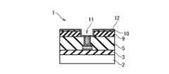
図2Aから2Fは、本発明の実施形態に係る半導体製造装置の製造方法において、タングステンプラグ7aを含む多層配線を形成する工程を説明するための半導体ウエハ1の断面図である。 2A to 2F are cross-sectional views of the
(工程S1)
図2Aに示される半導体ウエハ1に下層配線層4を形成する。図2Aに示される半導体ウエハ1は、基板2上に素子分離領域(図示されず)を形成し、トランジスタ(図示されず)を形成し、絶縁膜3を堆積し、絶縁膜3を平坦化し、絶縁膜3の上にコンタクト層(図示されず)を形成することで準備された。下層配線層4は、絶縁膜3の上に形成される。下層配線層4は、図2Bに示されるように、Ti膜上にTiN膜を積層したTiN/Ti膜4a、AlCu膜4b及びTiN膜4cからなる積層構造を有している。下層配線層4の中で、TiN/Ti膜4aは絶縁膜3に近い側に配置され、TiN膜4cは絶縁膜3に遠い側に配置され、AlCu膜4bはTiN/Ti膜4aとTiN膜4cとの間に配置されている。TiN/Ti膜4aは、絶縁膜3により近いチタン膜(Ti膜)とその上に配置された窒化チタン膜(TiN膜)とを含んでいる。例えば、TiN/Ti膜4aのチタン膜の厚さは20nm、TiN/Ti膜4aの窒化チタン膜の厚さは30nm、AlCu膜4bの厚さは300nm、TiN膜4cの厚さは50nmである。(Process S1)
A
(工程S2)
次に、層間絶縁膜としての絶縁膜5を半導体ウエハ1に形成する。絶縁膜5は、例えば、プラズマCVD(Chemical Vapor Deposition)法により形成されるシリコン酸化膜(SiO2膜)である。(Process S2)
Next, an insulating
(工程S3)
次に、CMP(Chemical Mechanical Polishing)法により絶縁膜5を平坦化する。(Process S3)
Next, the insulating
(工程S4)
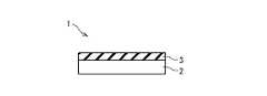
次に、絶縁膜5の窪み(凹部)としてのヴィアホール5aを形成する。ヴィアホール5aが形成された半導体ウエハ1が図2Cに示されている。ヴィアホール5aの底には下層配線層4が露出している。ヴィアホール5aが形成されていない絶縁膜5の部分は平坦部5bである。(Process S4)
Next, a via
(工程S5)
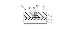
次に、絶縁膜5の上にバリア層6を形成する。バリア層6は、反応性スパッタ法で形成される窒化チタン膜(TiN膜)である。窒化チタン膜は、平坦部5b上の部分の膜厚が50nmになるように形成される。バリア層6は、窒化チタン膜の下地としてのチタン膜(Ti膜)を含んでもよい。バリア層6は、後の工程において耐熱性が要求されるため、高融点金属の窒化物膜であることが好ましい。高融点金属とは、例えば、チタン(Ti)、タングステン(Ta)及びモリブデン(Mo)である。(Process S5)
Next, the
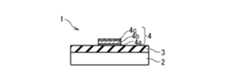
(工程S6)
次に、バリア層6の上にタングステン膜(W膜)7を形成する。タングステン膜7は、CVD法により堆積される、図2Dはタングステン膜7が形成された半導体ウエハ1を示している。タングステン膜7は、その一部がヴィアホール5aに埋め込まれ、他の部分が平坦部5bの上に配置されている。タングステン膜7は、他の部分の膜厚が400nmになるように形成される。ところで、タングステン膜7をCVD法により形成する際には、六フッ化タングステン(WF6)を含む原料ガスが用いられる。バリア層6により、WF6と下層配線層4が反応することが防がれる。また、絶縁膜5の上に直接タングステン膜7を形成した場合には絶縁膜5とタングステン膜7の密着性が問題となるが、これらの間にバリア層6が介在すると良好な密着性が得られる。(Step S6)
Next, a tungsten film (W film) 7 is formed on the
(工程S7)
次に、タングステン膜7をCMP法により研磨し、平坦部5bの上に配置されている他の部分を除去する。これにより、図2Eに示されるように、ヴィアホール5aに埋め込まれたタングステンプラグ7aが形成される。(Process S7)
Next, the
(工程S8)
次に、図2Fに示されるように、絶縁膜5の上に上層配線層8を形成する。上層配線層8は、タングステンプラグ7aに接続されるように形成される。上層配線層8は、TiN/Ti膜8a、AlCu膜8b及びTiN膜8cからなる積層構造を有している。上層配線層8の中で、TiN/Ti膜8aは絶縁膜5に近い側に配置され、TiN膜8cは絶縁膜5に遠い側に配置され、AlCu膜8bはTiN/Ti膜8aとTiN膜8cとの間に配置されている。TiN/Ti膜8aは、絶縁膜5により近いチタン膜(Ti膜)とその上に配置された窒化チタン膜(TiN膜)とを含んでいる。(Process S8)
Next, as shown in FIG. 2F, the
次に、図3から図12を参照して、本発明の実施形態に係る半導体装置の製造方法を詳細に説明する。 Next, with reference to FIGS. 3 to 12, a method for manufacturing a semiconductor device according to an embodiment of the present invention will be described in detail.
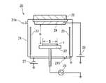
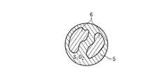
図3は、バリア層6を形成する工程(工程S5)に用いられる反応性スパッタ装置20の概略図である。反応性スパッタ装置20は、ガス導入口21a及びガス導出口21bが設けられた反応室21と、直流電源26及び27と、高周波電源28と、高周波電源28を介して接地されたサセプタ22と、直流電源27を介して接地されたシールド23と、直流電源26を介して接地されたターゲット24と、反応室21内に磁場を発生するマグネット25とを備えている。反応室21は、接地され、真空ポンプ(図示されず)により減圧自在である。サセプタ22、シールド23、及びターゲット24は、反応室21内に配置されている。ターゲット24はチタンターゲットである。サセプタ22は、半導体ウエハ1がターゲット24に対向するように半導体ウエハ1を保持する。直流電源26は、ターゲット24に直流の負電位を印加する。すなわち、直流電源26は、ターゲット24の電位を接地電位よりも低くする。直流電源27は、シールド23に直流の負電位を印加する。すなわち、直流電源27は、シールド23の電位を接地電位よりも低くする。高周波電源28は、高周波電力としてのRF(Radio Frequency)バイアスをサセプタ22に保持された半導体ウエハ1に印加する。また、温度制御装置(図示されず)により基板2の温度が制御される。 FIG. 3 is a schematic view of the
工程S5においては、アルゴンガス(Arガス)と窒素ガス(N2ガス)とを含む混合ガスをガス導入口21aから反応室21内に供給する。混合ガスを半導体ウエハ1の周辺部から中心部に向かう方向に流れるように半導体ウエハ1とターゲット24との間に導入しながら、半導体ウエハ1にRFバイアスを印加する。すると、反応室21内にプラズマが発生し、半導体ウエハ1上に窒化チタン膜が形成される。プラズマは、マグネット25が発生する磁場により一定の領域に閉じ込められる。窒化チタン膜の組成や結晶方位(配向性)のような膜質は、成膜条件によって異なる。導入された混合ガスに含まれる窒素ガスの一部はターゲット24中のチタンと結びついて消費される。窒素ガスの濃度が減少した(Arガスの比率が増加した)混合ガスは、半導体ウエハ1とターゲット24との間を半導体ウエハ1の中心部から周辺部に向かう方向に拡散し、ガス導出口21bから排出される。したがって、半導体ウエハ1とターゲット24との間には、半導体ウエハ1の周辺部に対応する領域で高く中心部に対応する領域で低い窒素ガス分圧の同心円状の分布が生じる。この窒素ガス分圧の分布は、ガス導入口21aから導入される混合ガスの総流量が小さいほど、また、半導体ウエハ1の直径Dが大きいほど顕著になる。半導体ウエハ1の直径Dが12インチ(300mm)以上の場合、窒素ガス分圧の分布は特に顕著になる。In step S5, a mixed gas containing argon gas (Ar gas) and nitrogen gas (N2 gas) is supplied into the
図4は、本発明の実施形態に係る半導体装置の製造方法における窒化チタン膜の成膜条件としての第1条件及び第3条件を示している。第2条件は、第1条件と比較するための成膜条件である。各条件について、成膜する窒化チタン膜の膜厚(膜厚)、成膜に要する時間(時間)、高周波電源28が印加するRFバイアスのパワー(パワー)、混合ガスの総流量中の窒素ガスの流量の比率(N2流量比)、混合ガス中のアルゴンガスの流量(Ar流量)、混合ガス中の窒素ガスの流量(N2流量)、半導体ウエハ1とターゲット24との間隔H(H)、及び半導体ウエハ1の直径D(D)が設定されている。FIG. 4 shows the first condition and the third condition as the conditions for forming the titanium nitride film in the method for manufacturing a semiconductor device according to the embodiment of the present invention. The second condition is a film forming condition for comparison with the first condition. For each condition, the film thickness (film thickness) of the titanium nitride film to be formed, the time (time) required for film formation, the RF bias power (power) applied by the high-
はじめに、第2条件でバリア層6としての窒化チタン膜を成膜した場合について説明する。第2条件においては、膜厚は50nm、時間は39sec、パワーは12kW、N2流量比は80.0%、Ar流量は24sccm、N2流量は96sccm、間隔Hは86mm、直径Dは300mmである。First, a case where a titanium nitride film as the
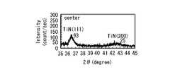
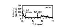
図5Aは、第2条件で成膜された窒化チタン膜のX線回折スペクトルを半導体ウエハ1の中心部で測定した結果を示すグラフである。図5Bは、第2条件で成膜された窒化チタン膜のX線回折スペクトルを半導体ウエハ1の周辺部で測定した結果を示すグラフである。ここで、窒化チタン膜は、チタンターゲットを用いた反応性DCマグネトロンスパッタ法で形成された。図5A及び5Bにおいて、縦軸はX線回折強度、横軸はX線回折角2θである。半導体ウエハ1の中心部においては、図5Aに示されるように、2θが約36.5度のところにTiN(111)の配向性を示すピークが観察され、2θが約42.5度のところにTiN(200)の配向性を示すピークが観察された。半導体ウエハ1の中心部においては、TiN(111)の配向性を示すピークにおけるX線回折強度は38count/s、TiN(200)の配向性を示すピークにおけるX線回折強度は82count/sであった。半導体ウエハ1の周辺部においては、図5Bに示されるよに、TiN(111)の配向性を示すピークは検出されず、2θが約42.5度のところにTiN(200)の配向性を示すピークが観察された。半導体ウエハ1の周辺部においては、TiN(200)の配向性を示すピークにおけるX線回折強度は140count/sであった。すなわち、第2条件で成膜された窒化チタン膜は、半導体ウエハ1の中心部においてはTiN(111)の配向性とTiN(200)の配向性とを有していたが、半導体ウエハ1の周辺部においてはTiN(111)の配向性を有さず、TiN(200)の配向性をより強く有していた。 FIG. 5A is a graph showing the results of measuring the X-ray diffraction spectrum of the titanium nitride film formed under the second condition at the center of the
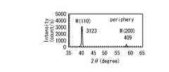
図6Aは、第2条件で成膜した窒化チタン膜の上に重ねて形成したタングステン膜7のX線回折スペクトルを半導体ウエハ1の中心部で測定した結果を示すグラフである。図6Bは、第2条件で成膜した窒化チタン膜の上に重ねて形成したタングステン膜7のX線回折スペクトルを半導体ウエハ1の周辺部で測定した結果を示すグラフである。ここで、タングステン膜7はCVD法で堆積された。図6A及び6Bにおいて、縦軸はX線回折強度、横軸はX線回折角2θである。タングステン膜7においては、図6A及び6Bに示されるように、2θが約40度のところにW(110)の配向性を示すピークが観察され、2θが約58.5度のところにW(200)の配向性を示すピークが観察された。半導体ウエハ1の中心部においては、図6Aに示されるように、W(110)の配向性を示すピークにおけるX線回折強度が3169count/sであったのに対し、W(200)の配向性を示すピークにおけるX線回折強度は592count/sと僅かであった。半導体ウエハ1の周辺部においては、図6Bに示されるように、W(110)の配向性を示すピークにおけるX線回折強度は1518count/s、W(200)の配向性を示すピークにおけるX線回折強度は4461count/sであった。すなわち、半導体ウエハ1の中心部においてはW(110)の配向性が主配向であったのに対し、半導体ウエハ1の周辺部においてはW(110)の配向性が弱くW(200)の配向性が強かった。 FIG. 6A is a graph showing the result of measuring the X-ray diffraction spectrum of the
図7は、第2条件で窒化チタン膜を成膜し、その上にタングステン膜7を成膜し、タングステン膜7にCMPを行った場合の半導体ウエハ1の上面図である。ここで、CMPは、半導体ウエハ1の中心部のタングステン膜7がジャストポリッシュされたところで終了した。CMPに要した時間は50秒であった。半導体ウエハ1全体に同じCMP処理を施したにも関わらず、ウエハの周辺部でタングステン膜7の膜残りが発生した。これは、同一のCMPの処理条件におけるタングステン膜7の研磨速度がW(110)の配向性を有する部分とW(200)の配向性を有する部分とで異なるためである。この処理条件におけるタングステン膜7の研磨速度は、W(200)の配向性を有する部分では200mm/min、W(110)の配向性を有する部分ではその2.5倍程度であった。したがって、タングステン膜7の配向性を半導体ウエハ1のウエハ面内において揃えることが均一な研磨速度を達成する上で重要である。すなわち、タングステン膜7の配向性を半導体ウエハ1のウエハ面内において一様にすることが重要である。 FIG. 7 is a top view of the
なお、半導体ウエハ1の周辺部のタングステン膜7を除去するためにCMPの処理時間を長く設定することは以下の理由から好ましくない。CMPの処理時間を長く設定すると、半導体ウエハ1の中心部においては絶縁膜5が研磨されて薄くなり、ヴィアホール5aの周囲で凹み(ディッシング)が大きくなる。その結果、下層配線層4と上層配線層8との間の寄生容量が増加し、下層配線層4及び上層配線層8を含む電気回路のRC時定数(Resistive−Capacitive time constant)が増加して信号伝播が遅延する。また、ディッシングにより半導体ウエハ1の被処理面(ウエハ面)に凹凸が形成されるため、露光プロセスにおける解像不良や、その後の加工プロセスにおける加工不良等の問題が生じる。 Note that it is not preferable to set the CMP processing time long in order to remove the
次に、第1条件でバリア層6としての窒化チタン膜を成膜した場合について説明する。第1条件においては、膜厚は50nm、時間は28sec、パワーは11kW、N2流量比は73.5%、Ar流量は18sccm、N2流量は50sccm、間隔Hは56mm、直径Dは300mmである。第1条件におけるN2流量比は、第2条件におけるN2流量比よりも小さい。第1条件で成膜すると、ストイキオメトリーよりもややチタンリッチな組成の窒化チタン膜が成膜される。Next, a case where a titanium nitride film as the
図8Aは、第1条件で成膜された窒化チタン膜のX線回折スペクトルを半導体ウエハ1の中心部で測定した結果を示すグラフである。図8Bは、第1条件で成膜された窒化チタン膜のX線回折スペクトルを半導体ウエハ1の周辺部で測定した結果を示すグラフである。ここで、窒化チタン膜は、チタンターゲットを用いた反応性DCマグネトロンスパッタ法で形成された。図8A及び8Bにおいて、縦軸はX線回折強度、横軸はX線回折角2θである。図8A及び8Bに示されるように、2θが約36.5度のところにTiN(111)の配向性を示すピークが観察され、2θが約42.5度のところにTiN(200)の配向性を示すピークが観察された。半導体ウエハ1の中心部においては、図8Aに示されるように、TiN(111)の配向性を示すピークにおけるX線回折強度は93count/s、TiN(200)の配向性を示すピークにおけるX線回折強度は25count/sであった。半導体ウエハ1の周辺部においては、図8Bに示されるように、TiN(111)の配向性を示すピークにおけるX線回折強度は49count/s、TiN(200)の配向性を示すピークにおけるX線回折強度は69count/sであった。すなわち、第1条件で成膜された窒化チタン膜は、半導体ウエハ1の中心部と周辺部の両方においてTiN(111)の配向性を有していた。 FIG. 8A is a graph showing the result of measuring the X-ray diffraction spectrum of the titanium nitride film formed under the first condition at the center of the
図9Aは、第1条件で成膜した窒化チタン膜の上に重ねて形成したタングステン膜7のX線回折スペクトルを半導体ウエハ1の中心部で測定した結果を示すグラフである。図9Bは、第1条件で成膜した窒化チタン膜の上に重ねて形成したタングステン膜7のX線回折スペクトルを半導体ウエハ1の周辺部で測定した結果を示すグラフである。ここで、タングステン膜7はCVD法で堆積された。図9A及び9Bにおいて、縦軸はX線回折強度、横軸はX線回折角2θである。タングステン膜7においては、図9A及び9Bに示されるように、2θが約40度のところにW(110)の配向性を示すピークが観察され、2θが約58.5度のところにW(200)の配向性を示すピークが観察された。半導体ウエハ1の中心部においては、図9Aに示されるように、W(110)の配向性を示すピークにおけるX線回折強度が6409count/s、W(200)の配向性を示すピークにおけるX線回折強度は321count/sであった。半導体ウエハ1の周辺部においては、図9Bに示されるように、W(110)の配向性を示すピークにおけるX線回折強度は3123count/s、W(200)の配向性を示すピークにおけるX線回折強度は409count/sであった。すなわち、半導体ウエハ1の中心部と周辺部との両方において、W(110)の配向性が主配向であった。 FIG. 9A is a graph showing the result of measuring the X-ray diffraction spectrum of the
図10は、第1条件で窒化チタン膜を成膜し、その上にタングステン膜7を成膜し、タングステン膜7にCMPを行った場合の半導体ウエハ1の上面図である。ここで、CMPは、半導体ウエハ1の中心部のタングステン膜7がジャストポリッシュされたところで終了した。図10に示されるように、タングステン膜7の膜残りは発生せず、半導体ウエハ1のウエハ面全体において絶縁膜5又はバリア層6が露出した。 FIG. 10 is a top view of the
次に、バリア層6としての窒化チタン膜を成膜する第3条件について説明する。第3条件においては、膜厚は50nm、時間は36sec、パワーは12kW、N2流量比は70.0%、Ar流量は60sccm、N2流量は140sccm、間隔Hは55mm、直径Dは300mmである。第3条件における混合ガスの総流量(Ar流量とN2流量とを合わせた流量)は、第1条件における混合ガスの総流量よりも大きい。混合ガスの総流量が大きいと半導体ウエハ1とターゲット24との間に生じる窒素ガス分圧の分布が緩和されるから、第3条件で成膜される窒化チタン膜は第1条件で成膜される窒化チタン膜よりも配向性が一様になる。Next, the third condition for forming a titanium nitride film as the
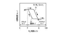
一般的には、工程S5における窒化チタン膜の成膜条件を以下のようにして設定することができる。工程S5における窒化チタン膜の成膜条件を設定する方法について、図11を参照して説明する。図11において、縦軸は窒化チタン膜の成膜速度、横軸はN2流量比である。反応性スパッタ装置20を用いて窒化チタン膜を成膜する際に、混合ガスの総流量及びRFバイアスを一定に保ちながら、N2流量比を変化させながら窒化チタン膜の成膜速度を測定すると曲線31及び32が観察される。曲線31は、N2流量比が増加しているときの成膜速度の変化を示す。曲線32は、N2流量比が減少しているときの成膜速度の変化を示す。N2流量比が0%より大きくP%より小さい範囲では、曲線31及び曲線32は互いに一致している。N2流量比が0%より大きくP%より小さい範囲をメタリックモードの範囲という。N2流量比がP%と等しいか大きく、且つ、Q%より小さいか等しい範囲では、曲線31及び曲線32は互いに一致しないでヒステリシスループを形成している。ここで、0<P<Q<100である。N2流量比がP%と等しいか大きく、且つ、Q%より小さいか等しい範囲を遷移モードの範囲という。N2流量比がQ%より大きく100%より小さい範囲では、曲線31及び曲線32は互いに一致している。N2流量比がQ%より大きく100%より小さい範囲をナイトライドモードの範囲という。In general, the conditions for forming the titanium nitride film in step S5 can be set as follows. A method for setting the film forming conditions of the titanium nitride film in step S5 will be described with reference to FIG. In FIG. 11, the vertical axis represents the deposition rate of the titanium nitride film, and the horizontal axis represents the N2 flow rate ratio. When the titanium nitride film is formed using the
ところで、N2流量比が大きいほど、ターゲット24の表面が窒化されて窒化チタン(TiN)が形成される。ターゲット24の表面が窒化されるとターゲット24のスパッタ率Sが低下し、半導体ウエハ1に堆積する窒化チタン膜の成膜速度が低下する。ここでスパッタ率Sは、ターゲット24に入射した粒子(イオン)の数をniとし、粒子によりスパッタされたターゲット24の原子(または分子)の数をnsとした場合、S=ns/niで定義される。したがって、遷移モードの範囲においては、ターゲット24の表面状態の影響により曲線31と曲線32とが一致しない履歴現象が観察される。遷移モードの範囲となる成膜条件で半導体ウエハ1に窒化チタン膜を形成すると、ターゲット24の周辺部で窒化が強く中心部で窒化が弱いため、窒化チタン膜の膜質がウエハ面全体で一様になりにくい。より具体的には、半導体ウエハ1の中心部と周辺部とで窒化チタン膜の配向性が異なり易い。半導体ウエハ1の直径が大きいと、半導体ウエハ1の中心部と周辺部とで窒化チタン膜の膜質が顕著に異なり易い。By the way, the larger the N2 flow rate ratio, the more the surface of the
ナイトライドモードの範囲となる成膜条件で半導体ウエハ1に窒化チタン膜を形成すると、窒化チタン膜はストイキオメトリーに近い組成となる。一方、メタリックモードの範囲となる成膜条件で半導体ウエハ1に窒化チタン膜を形成すると、窒化チタン膜はチタンリッチな組成となる。窒化チタン膜の下地である絶縁膜6がアモルファスのシリコン酸化膜(SiO2膜)の場合、ナイトライドモードの範囲となる成膜条件で成膜するとウエハ面全体でTiN(200)が主配向となりやすく、メタリックモードの範囲となる成膜条件で成膜するとウエハ面全体で組成がチタンリッチとなり且つ主配向がTiN(111)となりやすい。したがって、予備実験により図11に示されるデータを得ておいて、N2流量比が0%より大きく100%より小さい範囲から遷移モードの範囲を除いた範囲(メタリックモードの範囲又はナイトライドモードの範囲)となる成膜条件で窒化チタン膜を成膜すればよい。ウエハ面の全体で配向が一様な窒化チタン膜を形成するためには、導入される混合ガスの総流量、スパッタ圧力(反応室1内の圧力)、及び基板温度(基板2の温度)を、ターゲット24全体が一様に窒化された状態に保たれるように制御することが好ましい。このように、ウエハ面の全体で主配向が一様になるように窒化チタン膜を形成し、その上にCVD法でタングステン膜7を形成すると、タングステン膜7のCMPによる研磨速度がウエハ面の全体で一様になる。ゆえに、タングステン膜7の膜残りが防がれる。When a titanium nitride film is formed on the
バリア層6としての窒化チタン膜をウエハ面の全体で主配向が実質的に認められないように形成することでタングステン膜7の膜残りを防ぐことも可能である。主配向が実質的に認められないとは、主配向が認められないか、または極めて弱い主配向しか認められないことを意味する。 It is also possible to prevent the remaining film of the
バリア層6としての窒化チタン膜をウエハ面の全体で主配向が実質的に認められないように形成する方法として、高イオン化スパッタ法を用いた場合について説明する。高イオン化スパッタ法は、プラズマを用いる反応性スパッタ法である。高イオン化スパッタ法では、反応室内の圧力を低く制御し、イオン化率が高い条件で成膜する。高イオン化スパッタ法では、反応性スパッタ装置20を用い、反応室21内の圧力が0.5mTorrより高く2mTorrより低い圧力になるように制御し、半導体ウエハ1の基板温度が室温より高く50℃より低くなるように制御し、マグネット25によりターゲット24の表面近くに強い磁場を形成し、RFバイアスの周波数を40MHzより高く200MHzより低くなるように制御し、イオン化率を高めて窒化チタン膜を半導体ウエハ1に成膜する。周波数を200MHzより高くすることも可能であるが、その場合には反射波を抑えるためにインピーダンスのマッチングを調整することが重要となる。図12A及び12Bは、反応室21内の圧力が2mTorrをやや下回る低い圧力となるように制御し、半導体ウエハ1の基板温度が室温程度になるように制御した高イオン化スパッタ法により成膜した窒化チタン膜のX線回折スペクトルのグラフを示している。図12Aは、半導体ウエハ1の中心部で測定した結果を示している。図12Bは、半導体ウエハ1の周辺部で測定した結果を示している。図12A及び12Bにおいて、縦軸はX線回折強度、横軸はX線回折角2θである。TiN(111)の配向性及びTiN(200)の配向性に対応するX線回折角2θが、矢印で示されている。ウエハの中央部及び周辺部の両方において、特定の配向性は認められなかった。 As a method for forming the titanium nitride film as the
このように形成された窒化チタン膜の上にCVD法でタングステン膜7を形成すると、体心立方格子が最密構造であるタングステン膜7はウエハ面全体で弱いW(110)の配向性を有するように形成された。この場合も、タングステン膜7に対してCMPを行うと、第1条件で窒化チタン膜を成膜した場合と同様にタングステン膜7の膜残りは発生しなかった。 When the
高イオン化スパッタ法には、自己イオン化スパッタ法が含まれる。ヴィアホール5aにおいてバリア層6のカバレジ(被覆率)を適切にすることが可能であれば、通常のマグネトロンスパッタ法、ターゲットと基板との間隔を大きくして低圧で成膜する高指向性スパッタ法、コリメータを使用するスパッタ法、フラックスの指向性を電界で制御するスパッタ法を用いてもよい。 High ionization sputtering includes self-ionization sputtering. If the coverage (coverage) of the
これまで述べたように、ウエハ面の全体で膜質(配向性)が一様になるように窒化チタン膜をバリア層6として形成し、その上にタングステン膜7を形成することでウエハ面の全体でタングステン膜7の膜質(配向性)が一様になる。タングステン膜7の結晶構造は、下地材料の表面状態の影響を受けるためである。したがって、タングステン膜7に対してCMPを行うと、半導体ウエハ1の中心部と周辺部とにおいて同じ研磨速度でタングステン膜7が除去される。研磨不足によるタングステン膜7の膜残り、及び過剰研磨によるヴィアホール5aの周囲におけるディッシングの問題が解決される。ゆえに、チップ歩留まりが向上する。 As described above, the titanium nitride film is formed as the
窒化チタン膜は、CVD法により形成することも可能である。CVD法では原料ガスに由来する残留不純物の処理に注意を払う必要がある。チタンの有機物を含む原料ガスを用いると残留不純物としてカーボンが残るので、その後にプラズマ処理や加熱処理が必要である。チタンの塩化物を含む原料ガスを用いると塩素が窒化チタン膜の中に残留するので、その後に水素ガスを含む雰囲気中でのプラズマ処理が必要である。これらの処理を適切に行うことにより、CVD法をバリア層6の形成方法として適用できる。 The titanium nitride film can also be formed by a CVD method. In the CVD method, it is necessary to pay attention to the treatment of residual impurities derived from the source gas. When a source gas containing an organic material of titanium is used, carbon remains as a residual impurity, and plasma treatment or heat treatment is necessary thereafter. When a raw material gas containing titanium chloride is used, chlorine remains in the titanium nitride film, and plasma treatment in an atmosphere containing hydrogen gas is required thereafter. By performing these treatments appropriately, the CVD method can be applied as a method for forming the
次に、図13及び図14を参照して、本発明の実施形態に係る半導体装置の製造方法の変形例について説明する。 Next, with reference to FIG. 13 and FIG. 14, a modification of the method for manufacturing a semiconductor device according to the embodiment of the present invention will be described.
図13は、本発明の実施形態に係る半導体製造装置の製造方法の変形例を示すフロー図である。図13に示された工程S9から工程S14は、図1に示された工程S8のかわりに実行される。工程S9から工程S14は、上層配線層8のかわりに上層配線層13aを形成する工程である。上層配線層13aは、ダマシン法により形成される銅配線である。 FIG. 13 is a flowchart showing a modification of the manufacturing method of the semiconductor manufacturing apparatus according to the embodiment of the present invention. Steps S9 to S14 shown in FIG. 13 are executed instead of step S8 shown in FIG. Steps S <b> 9 to S <b> 14 are steps for forming the
図14Aから14Dは、本発明の実施形態に係る半導体製造装置の製造方法の変形例において、上層配線層13aを形成する工程を説明するための半導体ウエハの断面図である。 14A to 14D are cross-sectional views of a semiconductor wafer for explaining a process of forming an
(工程S9)
図2Eに示された半導体ウエハ1に絶縁膜9を形成する。絶縁膜9は、シリコン酸化膜であり、タングステンプラグ7aを覆うように絶縁膜5の上に形成される。(Process S9)
An insulating
(工程S10)
次に、絶縁膜9の上にシリコン窒化膜(SiN膜)10を形成する。(Step S10)
Next, a silicon nitride film (SiN film) 10 is formed on the insulating
(工程S11)
次に、絶縁膜9及びSiN膜10の窪み(凹部)としての配線溝11を形成する。絶縁膜9及びSiN膜10に配線溝11が形成された半導体ウエハ1が図14Aに示されている。配線溝11の底にはタングステンプラグ7aが露出している。配線溝11が形成されていないSiN膜10の部分は平坦部10bである。(Process S11)
Next, a
(工程S12)
次に、図14Bに示されるように、SiN膜10の上にバリア層12を形成する。バリア層12は、反応性スパッタ法で形成される窒化タンタル膜(TaN膜)である。バリア層12は、上述の窒化チタン膜を形成する方法と同様の方法により、配向性がウエハ面の全体で一様になるように形成される。この場合、タンタル(Ta)のターゲット24が用いられる。(Process S12)
Next, as shown in FIG. 14B, the
(工程S13)
次に、図14Cに示されるように、バリア層12の上に銅膜13を形成する。銅膜13は、メッキ法又はスパッタ法により形成される。銅膜13は、その一部が配線溝11に埋め込まれ、他の部分が平坦部10bの上に配置されている。銅膜13は、その結晶構造が下地であるバリア層12の状態の影響を受けるため、配向性がウエハ面の全体で一様になるように形成される。(Process S13)
Next, as shown in FIG. 14C, a
(工程S14)
次に、銅膜13をCMP法により研磨し、平坦部10bの上に配置されている他の部分を除去する。これにより、図14Dに示されるように、配線溝11に埋め込まれた上層配線層13aが形成される。上層配線層13aは、タングステンプラグ7aと接続されている。このとき、銅膜13の配向性がウエハ面の全体で一様であるため、半導体ウエハ1の中心部と周辺部とにおいて同じ研磨速度で銅膜13が除去される。したがって、研磨不足による銅膜13の膜残り、及び過剰研磨による配線溝11の周囲におけるディッシングの問題が解決される。ゆえに、チップ歩留まりが向上する。(Step S14)
Next, the
タングステンプラグ7a及び上層配線層13aをデュアルダマシン法により形成してもよい。 The
1…半導体ウエハ
2…基板
3、5、9…絶縁膜
4…下層配線層
4a…TiN/Ti膜
4b…AlCu膜
4c…TiN膜
5a…ヴィアホール
5b…平坦部
6、12…バリア層
7…タングステン膜
7a…タングステンプラグ
8…上層配線層
8a…TiN/Ti膜
8b…AlCu膜
8c…TiN膜
10…SiN膜
10b…平坦部
11…配線溝
13…銅膜
13a…上層配線層
20…反応性スパッタ装置
21…反応室
21a…ガス導入口
21b…ガス導出口
22…サセプタ
23…シールド
24…ターゲット
25…マグネット
26、27…直流電源
28…高周波電源
31、32…曲線DESCRIPTION OF
Claims (12)
Translated fromJapanese金属膜の第1部分が前記窪みに埋め込まれるように前記バリア層の上に前記金属膜を形成する工程と、
前記第1部分を残すように前記金属膜をCMP(Chemical Mechanical Polishing)法により研磨する工程と
を具備し、
前記絶縁膜は、半導体ウエハに形成され、
前記バリア層を形成する前記工程において、前記バリア層は、その配向性が前記半導体ウエハのウエハ面の全体で一様になるように形成される
半導体装置の製造方法。Forming a barrier layer on the insulating film provided with the depression;
Forming the metal film on the barrier layer such that a first portion of the metal film is embedded in the depression;
Polishing the metal film by a CMP (Chemical Mechanical Polishing) method so as to leave the first portion,
The insulating film is formed on a semiconductor wafer;
In the step of forming the barrier layer, the barrier layer is formed so that the orientation thereof is uniform over the entire wafer surface of the semiconductor wafer.
前記バリア層を形成する前記工程は、配向性が前記ウエハ面の全体で一様になるように前記金属窒化物膜を形成する工程を含む
請求項1に記載の半導体装置の製造方法。The barrier layer includes a metal nitride film as a refractory metal nitride film,
The method of manufacturing a semiconductor device according to claim 1, wherein the step of forming the barrier layer includes a step of forming the metal nitride film so that orientation is uniform over the entire wafer surface.
前記反応性スパッタ法において、
前記半導体ウエハと前記高融点金属のターゲットとが互いに対向するように反応室内に配置され、
アルゴンガスと窒素ガスとを含む混合ガスが、前記半導体ウエハの周辺部から中心部に向かう方向に流れるように、前記半導体ウエハと前記ターゲットとの間に導入され、
前記ターゲットに直流の負電位が印加され、
前記半導体ウエハに高周波電力が印加され、
前記混合ガスが含む窒素ガスの比率としての窒素ガス流量比は、0%より大きく100%より小さい範囲から所定の範囲を除いた範囲に属し、
前記所定の範囲は、前記窒素ガス流量比の変化に対する前記金属窒化物膜の成膜速度の変化において履歴現象が観察される範囲である
請求項2に記載の半導体装置の製造方法。In the step of forming the metal nitride film, the metal nitride film is formed by reactive sputtering,
In the reactive sputtering method,
The semiconductor wafer and the refractory metal target are disposed in a reaction chamber so as to face each other,
A mixed gas containing argon gas and nitrogen gas is introduced between the semiconductor wafer and the target so as to flow in a direction from the peripheral part to the central part of the semiconductor wafer,
A negative DC potential is applied to the target,
High frequency power is applied to the semiconductor wafer,
The nitrogen gas flow rate ratio as a ratio of nitrogen gas contained in the mixed gas belongs to a range excluding a predetermined range from a range larger than 0% and smaller than 100%,
The method for manufacturing a semiconductor device according to claim 2, wherein the predetermined range is a range in which a hysteresis phenomenon is observed in a change in the deposition rate of the metal nitride film with respect to a change in the nitrogen gas flow rate ratio.
前記所定の範囲を予備実験により求める前記工程は、
前記半導体ウエハとは別の半導体ウエハを、前記別の半導体ウエハと前記ターゲットとが対向するように前記反応室内に配置する工程と、
アルゴンガスと窒素ガスとを含む予備実験用の混合ガスを、前記別の半導体ウエハの周辺部から中心部に向かう方向に流れるように、前記別の半導体ウエハと前記ターゲットとの間に導入する工程と、
前記ターゲットに直流の負電位を印加する工程と、
前記別の半導体ウエハに高周波電力を印加する工程と、
前記別の半導体ウエハ上に形成される前記高融点金属の窒化物膜の成膜速度を測定する工程と、
前記成膜速度に基づいて前記所定の範囲を決定する工程と
を含み、
前記別の半導体ウエハと前記ターゲットとの間に導入する前記工程は、前記予備実験用の混合ガスが含む窒素ガスの比率を増加させながら前記予備実験用の混合ガスを導入する工程と、前記予備実験用の混合ガスが含む窒素ガスの比率を減少させながら前記予備実験用の混合ガスを導入する工程とを含む
請求項3に記載の半導体装置の製造方法。Comprising the step of determining the predetermined range by a preliminary experiment,
The step of obtaining the predetermined range by a preliminary experiment includes:
Disposing a semiconductor wafer different from the semiconductor wafer in the reaction chamber such that the other semiconductor wafer and the target face each other;
A step of introducing a mixed gas for a preliminary experiment including argon gas and nitrogen gas between the another semiconductor wafer and the target so as to flow in a direction from the peripheral part to the central part of the other semiconductor wafer. When,
Applying a negative DC potential to the target;
Applying high frequency power to the other semiconductor wafer;
Measuring a deposition rate of the refractory metal nitride film formed on the another semiconductor wafer;
Determining the predetermined range based on the deposition rate,
The step of introducing between the another semiconductor wafer and the target includes the step of introducing the preliminary experimental mixed gas while increasing the ratio of the nitrogen gas contained in the preliminary experimental mixed gas; The method for manufacturing a semiconductor device according to claim 3, further comprising: introducing the mixed gas for the preliminary experiment while reducing the ratio of the nitrogen gas included in the mixed gas for the experiment.
前記金属膜はタングステン膜であり、
前記金属膜を形成する前記工程において、
前記タングステン膜がCVD(Chemical Vapor Deposition)法により形成される
請求項2に記載の半導体装置の製造方法。The metal nitride film is a titanium nitride film;
The metal film is a tungsten film;
In the step of forming the metal film,
The method for manufacturing a semiconductor device according to claim 2, wherein the tungsten film is formed by a CVD (Chemical Vapor Deposition) method.
請求項5に記載の半導体装置の製造方法。The method for manufacturing a semiconductor device according to claim 5, wherein in the step of forming the metal nitride film, the titanium nitride film is formed by a sputtering method using self-ionized plasma.
前記半導体ウエハとチタンターゲットとが反応室内に配置され、
前記半導体ウエハの基板温度が室温より高く50℃より低くなるように制御され、
アルゴンガスと窒素ガスとを含む混合ガスが前記反応室内に導入され、
前記チタンターゲットに直流の負電位が印加され、
前記半導体ウエハに高周波電力が印加され、
前記高周波電力の周波数が40MHzより高く200MHzより低くなるように制御され、
前記反応室内の圧力が0.5mTorrより高く2mTorrより低くなるように制御される
請求項6に記載の半導体装置の製造方法。In the sputtering method,
The semiconductor wafer and the titanium target are disposed in a reaction chamber,
The substrate temperature of the semiconductor wafer is controlled to be higher than room temperature and lower than 50 ° C .;
A mixed gas containing argon gas and nitrogen gas is introduced into the reaction chamber,
A negative DC potential is applied to the titanium target,
High frequency power is applied to the semiconductor wafer,
The frequency of the high frequency power is controlled to be higher than 40 MHz and lower than 200 MHz,
The method for manufacturing a semiconductor device according to claim 6, wherein the pressure in the reaction chamber is controlled to be higher than 0.5 mTorr and lower than 2 mTorr.
前記バリア層を形成する前記工程は、自己イオン化プラズマを用いたスパッタ法により前記チタン膜を形成する工程を含み、
前記チタン膜を形成する前記工程は、前記高融点金属の窒化物膜を形成する前記工程の前に実行される
請求項6又は7に記載の半導体装置の製造方法。The barrier layer includes a titanium film,
The step of forming the barrier layer includes a step of forming the titanium film by sputtering using self-ionized plasma,
The method of manufacturing a semiconductor device according to claim 6, wherein the step of forming the titanium film is performed before the step of forming the nitride film of the refractory metal.
請求項1乃至8のいずれか1項に記載の半導体装置の製造方法。The method for manufacturing a semiconductor device according to claim 1, wherein the recess is a via hole of a multilayer wiring.
請求項2に記載の半導体装置の製造方法。The method for manufacturing a semiconductor device according to claim 2, wherein the recess is a groove for forming a wiring.
請求項10に記載の半導体装置の製造方法。The method for manufacturing a semiconductor device according to claim 10, wherein the metal film is a copper film.
請求項11に記載の半導体装置の製造方法。The method for manufacturing a semiconductor device according to claim 11, wherein the nitride film of the refractory metal is a tantalum nitride film.
Priority Applications (2)
| Application Number | Priority Date | Filing Date | Title |
|---|---|---|---|
| JP2006289442AJP2008108860A (en) | 2006-10-25 | 2006-10-25 | Manufacturing method of semiconductor device |
| US11/973,947US20080102630A1 (en) | 2006-10-25 | 2007-10-11 | Method of manufacturing semiconductor device |
Applications Claiming Priority (1)
| Application Number | Priority Date | Filing Date | Title |
|---|---|---|---|
| JP2006289442AJP2008108860A (en) | 2006-10-25 | 2006-10-25 | Manufacturing method of semiconductor device |
Publications (1)
| Publication Number | Publication Date |
|---|---|
| JP2008108860Atrue JP2008108860A (en) | 2008-05-08 |
Family
ID=39330761
Family Applications (1)
| Application Number | Title | Priority Date | Filing Date |
|---|---|---|---|
| JP2006289442APendingJP2008108860A (en) | 2006-10-25 | 2006-10-25 | Manufacturing method of semiconductor device |
Country Status (2)
| Country | Link |
|---|---|
| US (1) | US20080102630A1 (en) |
| JP (1) | JP2008108860A (en) |
Cited By (2)
| Publication number | Priority date | Publication date | Assignee | Title |
|---|---|---|---|---|
| JP2011222963A (en)* | 2010-01-15 | 2011-11-04 | Rohm Co Ltd | Semiconductor device and fabrication method for the same |
| KR20190113580A (en)* | 2018-03-27 | 2019-10-08 | 에이에스엠 아이피 홀딩 비.브이. | Method of forming an electrode on a substrate and a semiconductor device structure including an electrode |
Families Citing this family (276)
| Publication number | Priority date | Publication date | Assignee | Title |
|---|---|---|---|---|
| KR101923221B1 (en)* | 2007-12-07 | 2018-11-28 | 에바텍 아크티엔게젤샤프트 | Reactive sputtering with hipims |
| US20120199919A1 (en)* | 2009-07-29 | 2012-08-09 | Canon Anelva Corporation | Semiconductor device and method of manufacturing the same |
| CN102574399B (en) | 2009-10-28 | 2015-08-12 | 惠普发展公司,有限责任合伙企业 | Protective coatings for printhead feed slots |
| US20130023129A1 (en) | 2011-07-20 | 2013-01-24 | Asm America, Inc. | Pressure transmitter for a semiconductor processing environment |
| US10714315B2 (en) | 2012-10-12 | 2020-07-14 | Asm Ip Holdings B.V. | Semiconductor reaction chamber showerhead |
| US20160376700A1 (en) | 2013-02-01 | 2016-12-29 | Asm Ip Holding B.V. | System for treatment of deposition reactor |
| US11015245B2 (en) | 2014-03-19 | 2021-05-25 | Asm Ip Holding B.V. | Gas-phase reactor and system having exhaust plenum and components thereof |
| US10941490B2 (en) | 2014-10-07 | 2021-03-09 | Asm Ip Holding B.V. | Multiple temperature range susceptor, assembly, reactor and system including the susceptor, and methods of using the same |
| US10276355B2 (en) | 2015-03-12 | 2019-04-30 | Asm Ip Holding B.V. | Multi-zone reactor, system including the reactor, and method of using the same |
| US10458018B2 (en) | 2015-06-26 | 2019-10-29 | Asm Ip Holding B.V. | Structures including metal carbide material, devices including the structures, and methods of forming same |
| US10211308B2 (en) | 2015-10-21 | 2019-02-19 | Asm Ip Holding B.V. | NbMC layers |
| US11139308B2 (en) | 2015-12-29 | 2021-10-05 | Asm Ip Holding B.V. | Atomic layer deposition of III-V compounds to form V-NAND devices |
| US10529554B2 (en) | 2016-02-19 | 2020-01-07 | Asm Ip Holding B.V. | Method for forming silicon nitride film selectively on sidewalls or flat surfaces of trenches |
| US10343920B2 (en) | 2016-03-18 | 2019-07-09 | Asm Ip Holding B.V. | Aligned carbon nanotubes |
| US10367080B2 (en) | 2016-05-02 | 2019-07-30 | Asm Ip Holding B.V. | Method of forming a germanium oxynitride film |
| US11453943B2 (en) | 2016-05-25 | 2022-09-27 | Asm Ip Holding B.V. | Method for forming carbon-containing silicon/metal oxide or nitride film by ALD using silicon precursor and hydrocarbon precursor |
| US9859151B1 (en) | 2016-07-08 | 2018-01-02 | Asm Ip Holding B.V. | Selective film deposition method to form air gaps |
| US10612137B2 (en) | 2016-07-08 | 2020-04-07 | Asm Ip Holdings B.V. | Organic reactants for atomic layer deposition |
| US9812320B1 (en) | 2016-07-28 | 2017-11-07 | Asm Ip Holding B.V. | Method and apparatus for filling a gap |
| KR102532607B1 (en) | 2016-07-28 | 2023-05-15 | 에이에스엠 아이피 홀딩 비.브이. | Substrate processing apparatus and method of operating the same |
| US9887082B1 (en) | 2016-07-28 | 2018-02-06 | Asm Ip Holding B.V. | Method and apparatus for filling a gap |
| US11532757B2 (en) | 2016-10-27 | 2022-12-20 | Asm Ip Holding B.V. | Deposition of charge trapping layers |
| US10714350B2 (en) | 2016-11-01 | 2020-07-14 | ASM IP Holdings, B.V. | Methods for forming a transition metal niobium nitride film on a substrate by atomic layer deposition and related semiconductor device structures |
| KR102546317B1 (en) | 2016-11-15 | 2023-06-21 | 에이에스엠 아이피 홀딩 비.브이. | Gas supply unit and substrate processing apparatus including the same |
| KR102762543B1 (en) | 2016-12-14 | 2025-02-05 | 에이에스엠 아이피 홀딩 비.브이. | Substrate processing apparatus |
| US11447861B2 (en) | 2016-12-15 | 2022-09-20 | Asm Ip Holding B.V. | Sequential infiltration synthesis apparatus and a method of forming a patterned structure |
| US11581186B2 (en) | 2016-12-15 | 2023-02-14 | Asm Ip Holding B.V. | Sequential infiltration synthesis apparatus |
| KR102700194B1 (en) | 2016-12-19 | 2024-08-28 | 에이에스엠 아이피 홀딩 비.브이. | Substrate processing apparatus |
| US10269558B2 (en) | 2016-12-22 | 2019-04-23 | Asm Ip Holding B.V. | Method of forming a structure on a substrate |
| US11390950B2 (en) | 2017-01-10 | 2022-07-19 | Asm Ip Holding B.V. | Reactor system and method to reduce residue buildup during a film deposition process |
| US10468261B2 (en) | 2017-02-15 | 2019-11-05 | Asm Ip Holding B.V. | Methods for forming a metallic film on a substrate by cyclical deposition and related semiconductor device structures |
| US10529563B2 (en) | 2017-03-29 | 2020-01-07 | Asm Ip Holdings B.V. | Method for forming doped metal oxide films on a substrate by cyclical deposition and related semiconductor device structures |
| US10770286B2 (en) | 2017-05-08 | 2020-09-08 | Asm Ip Holdings B.V. | Methods for selectively forming a silicon nitride film on a substrate and related semiconductor device structures |
| US12040200B2 (en) | 2017-06-20 | 2024-07-16 | Asm Ip Holding B.V. | Semiconductor processing apparatus and methods for calibrating a semiconductor processing apparatus |
| US11306395B2 (en) | 2017-06-28 | 2022-04-19 | Asm Ip Holding B.V. | Methods for depositing a transition metal nitride film on a substrate by atomic layer deposition and related deposition apparatus |
| KR20190009245A (en) | 2017-07-18 | 2019-01-28 | 에이에스엠 아이피 홀딩 비.브이. | Methods for forming a semiconductor device structure and related semiconductor device structures |
| US11018002B2 (en) | 2017-07-19 | 2021-05-25 | Asm Ip Holding B.V. | Method for selectively depositing a Group IV semiconductor and related semiconductor device structures |
| US10541333B2 (en) | 2017-07-19 | 2020-01-21 | Asm Ip Holding B.V. | Method for depositing a group IV semiconductor and related semiconductor device structures |
| US11374112B2 (en) | 2017-07-19 | 2022-06-28 | Asm Ip Holding B.V. | Method for depositing a group IV semiconductor and related semiconductor device structures |
| US10590535B2 (en) | 2017-07-26 | 2020-03-17 | Asm Ip Holdings B.V. | Chemical treatment, deposition and/or infiltration apparatus and method for using the same |
| TWI815813B (en) | 2017-08-04 | 2023-09-21 | 荷蘭商Asm智慧財產控股公司 | Showerhead assembly for distributing a gas within a reaction chamber |
| US10692741B2 (en) | 2017-08-08 | 2020-06-23 | Asm Ip Holdings B.V. | Radiation shield |
| US10770336B2 (en) | 2017-08-08 | 2020-09-08 | Asm Ip Holding B.V. | Substrate lift mechanism and reactor including same |
| US11139191B2 (en) | 2017-08-09 | 2021-10-05 | Asm Ip Holding B.V. | Storage apparatus for storing cassettes for substrates and processing apparatus equipped therewith |
| US11769682B2 (en) | 2017-08-09 | 2023-09-26 | Asm Ip Holding B.V. | Storage apparatus for storing cassettes for substrates and processing apparatus equipped therewith |
| US11830730B2 (en) | 2017-08-29 | 2023-11-28 | Asm Ip Holding B.V. | Layer forming method and apparatus |
| KR102491945B1 (en) | 2017-08-30 | 2023-01-26 | 에이에스엠 아이피 홀딩 비.브이. | Substrate processing apparatus |
| US11295980B2 (en) | 2017-08-30 | 2022-04-05 | Asm Ip Holding B.V. | Methods for depositing a molybdenum metal film over a dielectric surface of a substrate by a cyclical deposition process and related semiconductor device structures |
| US11056344B2 (en) | 2017-08-30 | 2021-07-06 | Asm Ip Holding B.V. | Layer forming method |
| US10658205B2 (en) | 2017-09-28 | 2020-05-19 | Asm Ip Holdings B.V. | Chemical dispensing apparatus and methods for dispensing a chemical to a reaction chamber |
| US10403504B2 (en) | 2017-10-05 | 2019-09-03 | Asm Ip Holding B.V. | Method for selectively depositing a metallic film on a substrate |
| US10923344B2 (en) | 2017-10-30 | 2021-02-16 | Asm Ip Holding B.V. | Methods for forming a semiconductor structure and related semiconductor structures |
| US11022879B2 (en) | 2017-11-24 | 2021-06-01 | Asm Ip Holding B.V. | Method of forming an enhanced unexposed photoresist layer |
| CN111344522B (en) | 2017-11-27 | 2022-04-12 | 阿斯莫Ip控股公司 | Including clean mini-environment device |
| WO2019103613A1 (en) | 2017-11-27 | 2019-05-31 | Asm Ip Holding B.V. | A storage device for storing wafer cassettes for use with a batch furnace |
| US10872771B2 (en) | 2018-01-16 | 2020-12-22 | Asm Ip Holding B. V. | Method for depositing a material film on a substrate within a reaction chamber by a cyclical deposition process and related device structures |
| TWI799494B (en) | 2018-01-19 | 2023-04-21 | 荷蘭商Asm 智慧財產控股公司 | Deposition method |
| KR102695659B1 (en) | 2018-01-19 | 2024-08-14 | 에이에스엠 아이피 홀딩 비.브이. | Method for depositing a gap filling layer by plasma assisted deposition |
| US11081345B2 (en) | 2018-02-06 | 2021-08-03 | Asm Ip Holding B.V. | Method of post-deposition treatment for silicon oxide film |
| WO2019158960A1 (en) | 2018-02-14 | 2019-08-22 | Asm Ip Holding B.V. | A method for depositing a ruthenium-containing film on a substrate by a cyclical deposition process |
| US10896820B2 (en) | 2018-02-14 | 2021-01-19 | Asm Ip Holding B.V. | Method for depositing a ruthenium-containing film on a substrate by a cyclical deposition process |
| US10731249B2 (en) | 2018-02-15 | 2020-08-04 | Asm Ip Holding B.V. | Method of forming a transition metal containing film on a substrate by a cyclical deposition process, a method for supplying a transition metal halide compound to a reaction chamber, and related vapor deposition apparatus |
| KR102636427B1 (en) | 2018-02-20 | 2024-02-13 | 에이에스엠 아이피 홀딩 비.브이. | Substrate processing method and apparatus |
| US10975470B2 (en) | 2018-02-23 | 2021-04-13 | Asm Ip Holding B.V. | Apparatus for detecting or monitoring for a chemical precursor in a high temperature environment |
| US11473195B2 (en) | 2018-03-01 | 2022-10-18 | Asm Ip Holding B.V. | Semiconductor processing apparatus and a method for processing a substrate |
| US11629406B2 (en) | 2018-03-09 | 2023-04-18 | Asm Ip Holding B.V. | Semiconductor processing apparatus comprising one or more pyrometers for measuring a temperature of a substrate during transfer of the substrate |
| US11114283B2 (en) | 2018-03-16 | 2021-09-07 | Asm Ip Holding B.V. | Reactor, system including the reactor, and methods of manufacturing and using same |
| US11230766B2 (en) | 2018-03-29 | 2022-01-25 | Asm Ip Holding B.V. | Substrate processing apparatus and method |
| US11088002B2 (en) | 2018-03-29 | 2021-08-10 | Asm Ip Holding B.V. | Substrate rack and a substrate processing system and method |
| KR102600229B1 (en) | 2018-04-09 | 2023-11-10 | 에이에스엠 아이피 홀딩 비.브이. | Substrate supporting device, substrate processing apparatus including the same and substrate processing method |
| TWI811348B (en) | 2018-05-08 | 2023-08-11 | 荷蘭商Asm 智慧財產控股公司 | Methods for depositing an oxide film on a substrate by a cyclical deposition process and related device structures |
| US12025484B2 (en) | 2018-05-08 | 2024-07-02 | Asm Ip Holding B.V. | Thin film forming method |
| US12272527B2 (en) | 2018-05-09 | 2025-04-08 | Asm Ip Holding B.V. | Apparatus for use with hydrogen radicals and method of using same |
| KR102596988B1 (en) | 2018-05-28 | 2023-10-31 | 에이에스엠 아이피 홀딩 비.브이. | Method of processing a substrate and a device manufactured by the same |
| US11718913B2 (en) | 2018-06-04 | 2023-08-08 | Asm Ip Holding B.V. | Gas distribution system and reactor system including same |
| TWI840362B (en) | 2018-06-04 | 2024-05-01 | 荷蘭商Asm Ip私人控股有限公司 | Wafer handling chamber with moisture reduction |
| US11286562B2 (en) | 2018-06-08 | 2022-03-29 | Asm Ip Holding B.V. | Gas-phase chemical reactor and method of using same |
| US10797133B2 (en) | 2018-06-21 | 2020-10-06 | Asm Ip Holding B.V. | Method for depositing a phosphorus doped silicon arsenide film and related semiconductor device structures |
| KR102568797B1 (en) | 2018-06-21 | 2023-08-21 | 에이에스엠 아이피 홀딩 비.브이. | Substrate processing system |
| KR102854019B1 (en) | 2018-06-27 | 2025-09-02 | 에이에스엠 아이피 홀딩 비.브이. | Periodic deposition method for forming a metal-containing material and films and structures comprising the metal-containing material |
| TWI873894B (en) | 2018-06-27 | 2025-02-21 | 荷蘭商Asm Ip私人控股有限公司 | Cyclic deposition methods for forming metal-containing material and films and structures including the metal-containing material |
| US10612136B2 (en) | 2018-06-29 | 2020-04-07 | ASM IP Holding, B.V. | Temperature-controlled flange and reactor system including same |
| US10755922B2 (en) | 2018-07-03 | 2020-08-25 | Asm Ip Holding B.V. | Method for depositing silicon-free carbon-containing film as gap-fill layer by pulse plasma-assisted deposition |
| US10388513B1 (en) | 2018-07-03 | 2019-08-20 | Asm Ip Holding B.V. | Method for depositing silicon-free carbon-containing film as gap-fill layer by pulse plasma-assisted deposition |
| US11053591B2 (en) | 2018-08-06 | 2021-07-06 | Asm Ip Holding B.V. | Multi-port gas injection system and reactor system including same |
| US11430674B2 (en) | 2018-08-22 | 2022-08-30 | Asm Ip Holding B.V. | Sensor array, apparatus for dispensing a vapor phase reactant to a reaction chamber and related methods |
| US11024523B2 (en) | 2018-09-11 | 2021-06-01 | Asm Ip Holding B.V. | Substrate processing apparatus and method |
| KR102707956B1 (en) | 2018-09-11 | 2024-09-19 | 에이에스엠 아이피 홀딩 비.브이. | Method for deposition of a thin film |
| US11049751B2 (en) | 2018-09-14 | 2021-06-29 | Asm Ip Holding B.V. | Cassette supply system to store and handle cassettes and processing apparatus equipped therewith |
| CN110970344B (en) | 2018-10-01 | 2024-10-25 | Asmip控股有限公司 | Substrate holding apparatus, system comprising the same and method of using the same |
| US11232963B2 (en) | 2018-10-03 | 2022-01-25 | Asm Ip Holding B.V. | Substrate processing apparatus and method |
| KR102592699B1 (en) | 2018-10-08 | 2023-10-23 | 에이에스엠 아이피 홀딩 비.브이. | Substrate support unit and apparatuses for depositing thin film and processing the substrate including the same |
| KR102546322B1 (en) | 2018-10-19 | 2023-06-21 | 에이에스엠 아이피 홀딩 비.브이. | Substrate processing apparatus and substrate processing method |
| KR102605121B1 (en) | 2018-10-19 | 2023-11-23 | 에이에스엠 아이피 홀딩 비.브이. | Substrate processing apparatus and substrate processing method |
| USD948463S1 (en) | 2018-10-24 | 2022-04-12 | Asm Ip Holding B.V. | Susceptor for semiconductor substrate supporting apparatus |
| US12378665B2 (en) | 2018-10-26 | 2025-08-05 | Asm Ip Holding B.V. | High temperature coatings for a preclean and etch apparatus and related methods |
| US11087997B2 (en) | 2018-10-31 | 2021-08-10 | Asm Ip Holding B.V. | Substrate processing apparatus for processing substrates |
| KR102748291B1 (en) | 2018-11-02 | 2024-12-31 | 에이에스엠 아이피 홀딩 비.브이. | Substrate support unit and substrate processing apparatus including the same |
| US11572620B2 (en) | 2018-11-06 | 2023-02-07 | Asm Ip Holding B.V. | Methods for selectively depositing an amorphous silicon film on a substrate |
| US11031242B2 (en) | 2018-11-07 | 2021-06-08 | Asm Ip Holding B.V. | Methods for depositing a boron doped silicon germanium film |
| US10847366B2 (en) | 2018-11-16 | 2020-11-24 | Asm Ip Holding B.V. | Methods for depositing a transition metal chalcogenide film on a substrate by a cyclical deposition process |
| US10818758B2 (en) | 2018-11-16 | 2020-10-27 | Asm Ip Holding B.V. | Methods for forming a metal silicate film on a substrate in a reaction chamber and related semiconductor device structures |
| US12040199B2 (en) | 2018-11-28 | 2024-07-16 | Asm Ip Holding B.V. | Substrate processing apparatus for processing substrates |
| US11217444B2 (en) | 2018-11-30 | 2022-01-04 | Asm Ip Holding B.V. | Method for forming an ultraviolet radiation responsive metal oxide-containing film |
| KR102636428B1 (en) | 2018-12-04 | 2024-02-13 | 에이에스엠 아이피 홀딩 비.브이. | A method for cleaning a substrate processing apparatus |
| US11158513B2 (en) | 2018-12-13 | 2021-10-26 | Asm Ip Holding B.V. | Methods for forming a rhenium-containing film on a substrate by a cyclical deposition process and related semiconductor device structures |
| TWI874340B (en) | 2018-12-14 | 2025-03-01 | 荷蘭商Asm Ip私人控股有限公司 | Method of forming device structure, structure formed by the method and system for performing the method |
| TWI866480B (en) | 2019-01-17 | 2024-12-11 | 荷蘭商Asm Ip 私人控股有限公司 | Methods of forming a transition metal containing film on a substrate by a cyclical deposition process |
| KR102727227B1 (en) | 2019-01-22 | 2024-11-07 | 에이에스엠 아이피 홀딩 비.브이. | Semiconductor processing device |
| CN111524788B (en) | 2019-02-01 | 2023-11-24 | Asm Ip私人控股有限公司 | Method for forming topologically selective films of silicon oxide |
| KR102626263B1 (en) | 2019-02-20 | 2024-01-16 | 에이에스엠 아이피 홀딩 비.브이. | Cyclical deposition method including treatment step and apparatus for same |
| TWI873122B (en) | 2019-02-20 | 2025-02-21 | 荷蘭商Asm Ip私人控股有限公司 | Method of filling a recess formed within a surface of a substrate, semiconductor structure formed according to the method, and semiconductor processing apparatus |
| TWI845607B (en) | 2019-02-20 | 2024-06-21 | 荷蘭商Asm Ip私人控股有限公司 | Cyclical deposition method and apparatus for filling a recess formed within a substrate surface |
| TWI838458B (en) | 2019-02-20 | 2024-04-11 | 荷蘭商Asm Ip私人控股有限公司 | Apparatus and methods for plug fill deposition in 3-d nand applications |
| TWI842826B (en) | 2019-02-22 | 2024-05-21 | 荷蘭商Asm Ip私人控股有限公司 | Substrate processing apparatus and method for processing substrate |
| US11742198B2 (en) | 2019-03-08 | 2023-08-29 | Asm Ip Holding B.V. | Structure including SiOCN layer and method of forming same |
| KR102858005B1 (en) | 2019-03-08 | 2025-09-09 | 에이에스엠 아이피 홀딩 비.브이. | Method for Selective Deposition of Silicon Nitride Layer and Structure Including Selectively-Deposited Silicon Nitride Layer |
| KR102782593B1 (en) | 2019-03-08 | 2025-03-14 | 에이에스엠 아이피 홀딩 비.브이. | Structure Including SiOC Layer and Method of Forming Same |
| JP2020167398A (en) | 2019-03-28 | 2020-10-08 | エーエスエム・アイピー・ホールディング・ベー・フェー | Door openers and substrate processing equipment provided with door openers |
| KR102809999B1 (en) | 2019-04-01 | 2025-05-19 | 에이에스엠 아이피 홀딩 비.브이. | Method of manufacturing semiconductor device |
| KR20200123380A (en) | 2019-04-19 | 2020-10-29 | 에이에스엠 아이피 홀딩 비.브이. | Layer forming method and apparatus |
| KR20200125453A (en) | 2019-04-24 | 2020-11-04 | 에이에스엠 아이피 홀딩 비.브이. | Gas-phase reactor system and method of using same |
| KR20200130121A (en) | 2019-05-07 | 2020-11-18 | 에이에스엠 아이피 홀딩 비.브이. | Chemical source vessel with dip tube |
| US11289326B2 (en) | 2019-05-07 | 2022-03-29 | Asm Ip Holding B.V. | Method for reforming amorphous carbon polymer film |
| KR20200130652A (en) | 2019-05-10 | 2020-11-19 | 에이에스엠 아이피 홀딩 비.브이. | Method of depositing material onto a surface and structure formed according to the method |
| JP7598201B2 (en) | 2019-05-16 | 2024-12-11 | エーエスエム・アイピー・ホールディング・ベー・フェー | Wafer boat handling apparatus, vertical batch furnace and method |
| JP7612342B2 (en) | 2019-05-16 | 2025-01-14 | エーエスエム・アイピー・ホールディング・ベー・フェー | Wafer boat handling apparatus, vertical batch furnace and method |
| USD975665S1 (en) | 2019-05-17 | 2023-01-17 | Asm Ip Holding B.V. | Susceptor shaft |
| USD947913S1 (en) | 2019-05-17 | 2022-04-05 | Asm Ip Holding B.V. | Susceptor shaft |
| USD935572S1 (en) | 2019-05-24 | 2021-11-09 | Asm Ip Holding B.V. | Gas channel plate |
| USD922229S1 (en) | 2019-06-05 | 2021-06-15 | Asm Ip Holding B.V. | Device for controlling a temperature of a gas supply unit |
| KR20200141002A (en) | 2019-06-06 | 2020-12-17 | 에이에스엠 아이피 홀딩 비.브이. | Method of using a gas-phase reactor system including analyzing exhausted gas |
| KR20200141931A (en) | 2019-06-10 | 2020-12-21 | 에이에스엠 아이피 홀딩 비.브이. | Method for cleaning quartz epitaxial chambers |
| KR20200143254A (en) | 2019-06-11 | 2020-12-23 | 에이에스엠 아이피 홀딩 비.브이. | Method of forming an electronic structure using an reforming gas, system for performing the method, and structure formed using the method |
| USD944946S1 (en) | 2019-06-14 | 2022-03-01 | Asm Ip Holding B.V. | Shower plate |
| USD931978S1 (en) | 2019-06-27 | 2021-09-28 | Asm Ip Holding B.V. | Showerhead vacuum transport |
| KR20210005515A (en) | 2019-07-03 | 2021-01-14 | 에이에스엠 아이피 홀딩 비.브이. | Temperature control assembly for substrate processing apparatus and method of using same |
| JP7499079B2 (en) | 2019-07-09 | 2024-06-13 | エーエスエム・アイピー・ホールディング・ベー・フェー | Plasma device using coaxial waveguide and substrate processing method |
| CN112216646A (en) | 2019-07-10 | 2021-01-12 | Asm Ip私人控股有限公司 | Substrate supporting assembly and substrate processing device comprising same |
| KR20210010307A (en) | 2019-07-16 | 2021-01-27 | 에이에스엠 아이피 홀딩 비.브이. | Substrate processing apparatus |
| KR20210010816A (en) | 2019-07-17 | 2021-01-28 | 에이에스엠 아이피 홀딩 비.브이. | Radical assist ignition plasma system and method |
| KR102860110B1 (en) | 2019-07-17 | 2025-09-16 | 에이에스엠 아이피 홀딩 비.브이. | Methods of forming silicon germanium structures |
| US11643724B2 (en) | 2019-07-18 | 2023-05-09 | Asm Ip Holding B.V. | Method of forming structures using a neutral beam |
| KR20210010817A (en) | 2019-07-19 | 2021-01-28 | 에이에스엠 아이피 홀딩 비.브이. | Method of Forming Topology-Controlled Amorphous Carbon Polymer Film |
| TWI839544B (en) | 2019-07-19 | 2024-04-21 | 荷蘭商Asm Ip私人控股有限公司 | Method of forming topology-controlled amorphous carbon polymer film |
| TWI851767B (en) | 2019-07-29 | 2024-08-11 | 荷蘭商Asm Ip私人控股有限公司 | Methods for selective deposition utilizing n-type dopants and/or alternative dopants to achieve high dopant incorporation |
| CN112309899A (en) | 2019-07-30 | 2021-02-02 | Asm Ip私人控股有限公司 | Substrate processing apparatus |
| US12169361B2 (en) | 2019-07-30 | 2024-12-17 | Asm Ip Holding B.V. | Substrate processing apparatus and method |
| CN112309900A (en) | 2019-07-30 | 2021-02-02 | Asm Ip私人控股有限公司 | Substrate processing apparatus |
| US11227782B2 (en) | 2019-07-31 | 2022-01-18 | Asm Ip Holding B.V. | Vertical batch furnace assembly |
| US11587814B2 (en) | 2019-07-31 | 2023-02-21 | Asm Ip Holding B.V. | Vertical batch furnace assembly |
| US11587815B2 (en) | 2019-07-31 | 2023-02-21 | Asm Ip Holding B.V. | Vertical batch furnace assembly |
| CN112323048B (en) | 2019-08-05 | 2024-02-09 | Asm Ip私人控股有限公司 | Liquid level sensor for chemical source container |
| CN112342526A (en) | 2019-08-09 | 2021-02-09 | Asm Ip私人控股有限公司 | Heater assembly including cooling device and method of using same |
| USD965524S1 (en) | 2019-08-19 | 2022-10-04 | Asm Ip Holding B.V. | Susceptor support |
| USD965044S1 (en) | 2019-08-19 | 2022-09-27 | Asm Ip Holding B.V. | Susceptor shaft |
| JP2021031769A (en) | 2019-08-21 | 2021-03-01 | エーエスエム アイピー ホールディング ビー.ブイ. | Production apparatus of mixed gas of film deposition raw material and film deposition apparatus |
| USD940837S1 (en) | 2019-08-22 | 2022-01-11 | Asm Ip Holding B.V. | Electrode |
| USD949319S1 (en) | 2019-08-22 | 2022-04-19 | Asm Ip Holding B.V. | Exhaust duct |
| USD930782S1 (en) | 2019-08-22 | 2021-09-14 | Asm Ip Holding B.V. | Gas distributor |
| KR20210024423A (en) | 2019-08-22 | 2021-03-05 | 에이에스엠 아이피 홀딩 비.브이. | Method for forming a structure with a hole |
| USD979506S1 (en) | 2019-08-22 | 2023-02-28 | Asm Ip Holding B.V. | Insulator |
| KR20210024420A (en) | 2019-08-23 | 2021-03-05 | 에이에스엠 아이피 홀딩 비.브이. | Method for depositing silicon oxide film having improved quality by peald using bis(diethylamino)silane |
| US11286558B2 (en) | 2019-08-23 | 2022-03-29 | Asm Ip Holding B.V. | Methods for depositing a molybdenum nitride film on a surface of a substrate by a cyclical deposition process and related semiconductor device structures including a molybdenum nitride film |
| KR102806450B1 (en) | 2019-09-04 | 2025-05-12 | 에이에스엠 아이피 홀딩 비.브이. | Methods for selective deposition using a sacrificial capping layer |
| KR102733104B1 (en) | 2019-09-05 | 2024-11-22 | 에이에스엠 아이피 홀딩 비.브이. | Substrate processing apparatus |
| US11562901B2 (en) | 2019-09-25 | 2023-01-24 | Asm Ip Holding B.V. | Substrate processing method |
| CN112593212B (en) | 2019-10-02 | 2023-12-22 | Asm Ip私人控股有限公司 | Method for forming topologically selective silicon oxide film by cyclic plasma enhanced deposition process |
| TWI846953B (en) | 2019-10-08 | 2024-07-01 | 荷蘭商Asm Ip私人控股有限公司 | Substrate processing device |
| KR20210042810A (en) | 2019-10-08 | 2021-04-20 | 에이에스엠 아이피 홀딩 비.브이. | Reactor system including a gas distribution assembly for use with activated species and method of using same |
| TW202128273A (en) | 2019-10-08 | 2021-08-01 | 荷蘭商Asm Ip私人控股有限公司 | Gas injection system, reactor system, and method of depositing material on surface of substratewithin reaction chamber |
| TWI846966B (en) | 2019-10-10 | 2024-07-01 | 荷蘭商Asm Ip私人控股有限公司 | Method of forming a photoresist underlayer and structure including same |
| US12009241B2 (en) | 2019-10-14 | 2024-06-11 | Asm Ip Holding B.V. | Vertical batch furnace assembly with detector to detect cassette |
| TWI834919B (en) | 2019-10-16 | 2024-03-11 | 荷蘭商Asm Ip私人控股有限公司 | Method of topology-selective film formation of silicon oxide |
| US11637014B2 (en) | 2019-10-17 | 2023-04-25 | Asm Ip Holding B.V. | Methods for selective deposition of doped semiconductor material |
| KR102845724B1 (en) | 2019-10-21 | 2025-08-13 | 에이에스엠 아이피 홀딩 비.브이. | Apparatus and methods for selectively etching films |
| KR20210050453A (en) | 2019-10-25 | 2021-05-07 | 에이에스엠 아이피 홀딩 비.브이. | Methods for filling a gap feature on a substrate surface and related semiconductor structures |
| US11646205B2 (en) | 2019-10-29 | 2023-05-09 | Asm Ip Holding B.V. | Methods of selectively forming n-type doped material on a surface, systems for selectively forming n-type doped material, and structures formed using same |
| KR20210054983A (en) | 2019-11-05 | 2021-05-14 | 에이에스엠 아이피 홀딩 비.브이. | Structures with doped semiconductor layers and methods and systems for forming same |
| US11501968B2 (en) | 2019-11-15 | 2022-11-15 | Asm Ip Holding B.V. | Method for providing a semiconductor device with silicon filled gaps |
| KR102861314B1 (en) | 2019-11-20 | 2025-09-17 | 에이에스엠 아이피 홀딩 비.브이. | Method of depositing carbon-containing material on a surface of a substrate, structure formed using the method, and system for forming the structure |
| CN112951697B (en) | 2019-11-26 | 2025-07-29 | Asmip私人控股有限公司 | Substrate processing apparatus |
| US11450529B2 (en) | 2019-11-26 | 2022-09-20 | Asm Ip Holding B.V. | Methods for selectively forming a target film on a substrate comprising a first dielectric surface and a second metallic surface |
| CN112885692B (en) | 2019-11-29 | 2025-08-15 | Asmip私人控股有限公司 | Substrate processing apparatus |
| CN120432376A (en) | 2019-11-29 | 2025-08-05 | Asm Ip私人控股有限公司 | Substrate processing apparatus |
| JP7527928B2 (en) | 2019-12-02 | 2024-08-05 | エーエスエム・アイピー・ホールディング・ベー・フェー | Substrate processing apparatus and substrate processing method |
| KR20210070898A (en) | 2019-12-04 | 2021-06-15 | 에이에스엠 아이피 홀딩 비.브이. | Substrate processing apparatus |
| KR20210078405A (en) | 2019-12-17 | 2021-06-28 | 에이에스엠 아이피 홀딩 비.브이. | Method of forming vanadium nitride layer and structure including the vanadium nitride layer |
| KR20210080214A (en) | 2019-12-19 | 2021-06-30 | 에이에스엠 아이피 홀딩 비.브이. | Methods for filling a gap feature on a substrate and related semiconductor structures |
| JP7730637B2 (en) | 2020-01-06 | 2025-08-28 | エーエスエム・アイピー・ホールディング・ベー・フェー | Gas delivery assembly, components thereof, and reactor system including same |
| JP7636892B2 (en) | 2020-01-06 | 2025-02-27 | エーエスエム・アイピー・ホールディング・ベー・フェー | Channeled Lift Pins |
| US11993847B2 (en) | 2020-01-08 | 2024-05-28 | Asm Ip Holding B.V. | Injector |
| KR20210093163A (en) | 2020-01-16 | 2021-07-27 | 에이에스엠 아이피 홀딩 비.브이. | Method of forming high aspect ratio features |
| KR102675856B1 (en) | 2020-01-20 | 2024-06-17 | 에이에스엠 아이피 홀딩 비.브이. | Method of forming thin film and method of modifying surface of thin film |
| TWI889744B (en) | 2020-01-29 | 2025-07-11 | 荷蘭商Asm Ip私人控股有限公司 | Contaminant trap system, and baffle plate stack |
| TW202513845A (en) | 2020-02-03 | 2025-04-01 | 荷蘭商Asm Ip私人控股有限公司 | Semiconductor structures and methods for forming the same |
| KR20210100010A (en) | 2020-02-04 | 2021-08-13 | 에이에스엠 아이피 홀딩 비.브이. | Method and apparatus for transmittance measurements of large articles |
| US11776846B2 (en) | 2020-02-07 | 2023-10-03 | Asm Ip Holding B.V. | Methods for depositing gap filling fluids and related systems and devices |
| KR20210103956A (en) | 2020-02-13 | 2021-08-24 | 에이에스엠 아이피 홀딩 비.브이. | Substrate processing apparatus including light receiving device and calibration method of light receiving device |
| TW202146691A (en) | 2020-02-13 | 2021-12-16 | 荷蘭商Asm Ip私人控股有限公司 | Gas distribution assembly, shower plate assembly, and method of adjusting conductance of gas to reaction chamber |
| TWI855223B (en) | 2020-02-17 | 2024-09-11 | 荷蘭商Asm Ip私人控股有限公司 | Method for growing phosphorous-doped silicon layer |
| CN113410160A (en) | 2020-02-28 | 2021-09-17 | Asm Ip私人控股有限公司 | System specially used for cleaning parts |
| KR20210113043A (en) | 2020-03-04 | 2021-09-15 | 에이에스엠 아이피 홀딩 비.브이. | Alignment fixture for a reactor system |
| US11876356B2 (en) | 2020-03-11 | 2024-01-16 | Asm Ip Holding B.V. | Lockout tagout assembly and system and method of using same |
| KR20210116240A (en) | 2020-03-11 | 2021-09-27 | 에이에스엠 아이피 홀딩 비.브이. | Substrate handling device with adjustable joints |
| KR102775390B1 (en) | 2020-03-12 | 2025-02-28 | 에이에스엠 아이피 홀딩 비.브이. | Method for Fabricating Layer Structure Having Target Topological Profile |
| US12173404B2 (en) | 2020-03-17 | 2024-12-24 | Asm Ip Holding B.V. | Method of depositing epitaxial material, structure formed using the method, and system for performing the method |
| KR102755229B1 (en) | 2020-04-02 | 2025-01-14 | 에이에스엠 아이피 홀딩 비.브이. | Thin film forming method |
| TWI887376B (en) | 2020-04-03 | 2025-06-21 | 荷蘭商Asm Ip私人控股有限公司 | Method for manufacturing semiconductor device |
| TWI888525B (en) | 2020-04-08 | 2025-07-01 | 荷蘭商Asm Ip私人控股有限公司 | Apparatus and methods for selectively etching silcon oxide films |
| US11821078B2 (en) | 2020-04-15 | 2023-11-21 | Asm Ip Holding B.V. | Method for forming precoat film and method for forming silicon-containing film |
| KR20210128343A (en) | 2020-04-15 | 2021-10-26 | 에이에스엠 아이피 홀딩 비.브이. | Method of forming chromium nitride layer and structure including the chromium nitride layer |
| US11996289B2 (en) | 2020-04-16 | 2024-05-28 | Asm Ip Holding B.V. | Methods of forming structures including silicon germanium and silicon layers, devices formed using the methods, and systems for performing the methods |
| KR20210130646A (en) | 2020-04-21 | 2021-11-01 | 에이에스엠 아이피 홀딩 비.브이. | Method for processing a substrate |
| KR20210132612A (en) | 2020-04-24 | 2021-11-04 | 에이에스엠 아이피 홀딩 비.브이. | Methods and apparatus for stabilizing vanadium compounds |
| KR102866804B1 (en) | 2020-04-24 | 2025-09-30 | 에이에스엠 아이피 홀딩 비.브이. | Vertical batch furnace assembly comprising a cooling gas supply |
| CN113555279A (en) | 2020-04-24 | 2021-10-26 | Asm Ip私人控股有限公司 | Methods of forming vanadium nitride-containing layers and structures comprising the same |
| TW202208671A (en) | 2020-04-24 | 2022-03-01 | 荷蘭商Asm Ip私人控股有限公司 | Methods of forming structures including vanadium boride and vanadium phosphide layers |
| KR20210132600A (en) | 2020-04-24 | 2021-11-04 | 에이에스엠 아이피 홀딩 비.브이. | Methods and systems for depositing a layer comprising vanadium, nitrogen, and a further element |
| KR102783898B1 (en) | 2020-04-29 | 2025-03-18 | 에이에스엠 아이피 홀딩 비.브이. | Solid source precursor vessel |
| KR20210134869A (en) | 2020-05-01 | 2021-11-11 | 에이에스엠 아이피 홀딩 비.브이. | Fast FOUP swapping with a FOUP handler |
| JP7726664B2 (en) | 2020-05-04 | 2025-08-20 | エーエスエム・アイピー・ホールディング・ベー・フェー | Substrate processing system for processing a substrate |
| KR102788543B1 (en) | 2020-05-13 | 2025-03-27 | 에이에스엠 아이피 홀딩 비.브이. | Laser alignment fixture for a reactor system |
| TW202146699A (en) | 2020-05-15 | 2021-12-16 | 荷蘭商Asm Ip私人控股有限公司 | Method of forming a silicon germanium layer, semiconductor structure, semiconductor device, method of forming a deposition layer, and deposition system |
| KR20210143653A (en) | 2020-05-19 | 2021-11-29 | 에이에스엠 아이피 홀딩 비.브이. | Substrate processing apparatus |
| KR102795476B1 (en) | 2020-05-21 | 2025-04-11 | 에이에스엠 아이피 홀딩 비.브이. | Structures including multiple carbon layers and methods of forming and using same |
| KR20210145079A (en) | 2020-05-21 | 2021-12-01 | 에이에스엠 아이피 홀딩 비.브이. | Flange and apparatus for processing substrates |
| TWI873343B (en) | 2020-05-22 | 2025-02-21 | 荷蘭商Asm Ip私人控股有限公司 | Reaction system for forming thin film on substrate |
| KR20210146802A (en) | 2020-05-26 | 2021-12-06 | 에이에스엠 아이피 홀딩 비.브이. | Method for depositing boron and gallium containing silicon germanium layers |
| TWI876048B (en) | 2020-05-29 | 2025-03-11 | 荷蘭商Asm Ip私人控股有限公司 | Substrate processing device |
| TW202212620A (en) | 2020-06-02 | 2022-04-01 | 荷蘭商Asm Ip私人控股有限公司 | Apparatus for processing substrate, method of forming film, and method of controlling apparatus for processing substrate |
| TW202208659A (en) | 2020-06-16 | 2022-03-01 | 荷蘭商Asm Ip私人控股有限公司 | Method for depositing boron containing silicon germanium layers |
| TW202218133A (en) | 2020-06-24 | 2022-05-01 | 荷蘭商Asm Ip私人控股有限公司 | Method for forming a layer provided with silicon |
| TWI873359B (en) | 2020-06-30 | 2025-02-21 | 荷蘭商Asm Ip私人控股有限公司 | Substrate processing method |
| US12431354B2 (en) | 2020-07-01 | 2025-09-30 | Asm Ip Holding B.V. | Silicon nitride and silicon oxide deposition methods using fluorine inhibitor |
| TW202202649A (en) | 2020-07-08 | 2022-01-16 | 荷蘭商Asm Ip私人控股有限公司 | Substrate processing method |
| KR20220010438A (en) | 2020-07-17 | 2022-01-25 | 에이에스엠 아이피 홀딩 비.브이. | Structures and methods for use in photolithography |
| TWI878570B (en) | 2020-07-20 | 2025-04-01 | 荷蘭商Asm Ip私人控股有限公司 | Method and system for depositing molybdenum layers |
| KR20220011092A (en) | 2020-07-20 | 2022-01-27 | 에이에스엠 아이피 홀딩 비.브이. | Method and system for forming structures including transition metal layers |
| US12322591B2 (en) | 2020-07-27 | 2025-06-03 | Asm Ip Holding B.V. | Thin film deposition process |
| KR20220021863A (en) | 2020-08-14 | 2022-02-22 | 에이에스엠 아이피 홀딩 비.브이. | Method for processing a substrate |
| US12040177B2 (en) | 2020-08-18 | 2024-07-16 | Asm Ip Holding B.V. | Methods for forming a laminate film by cyclical plasma-enhanced deposition processes |
| TW202228863A (en) | 2020-08-25 | 2022-08-01 | 荷蘭商Asm Ip私人控股有限公司 | Method for cleaning a substrate, method for selectively depositing, and reaction system |
| US11725280B2 (en) | 2020-08-26 | 2023-08-15 | Asm Ip Holding B.V. | Method for forming metal silicon oxide and metal silicon oxynitride layers |
| TW202229601A (en) | 2020-08-27 | 2022-08-01 | 荷蘭商Asm Ip私人控股有限公司 | Method of forming patterned structures, method of manipulating mechanical property, device structure, and substrate processing system |
| TW202217045A (en) | 2020-09-10 | 2022-05-01 | 荷蘭商Asm Ip私人控股有限公司 | Methods for depositing gap filing fluids and related systems and devices |
| USD990534S1 (en) | 2020-09-11 | 2023-06-27 | Asm Ip Holding B.V. | Weighted lift pin |
| US11955379B2 (en)* | 2020-09-15 | 2024-04-09 | Taiwan Semiconductor Manufacturing Company, Ltd. | Metal adhesion layer to promote metal plug adhesion |
| KR20220036866A (en) | 2020-09-16 | 2022-03-23 | 에이에스엠 아이피 홀딩 비.브이. | Silicon oxide deposition method |
| USD1012873S1 (en) | 2020-09-24 | 2024-01-30 | Asm Ip Holding B.V. | Electrode for semiconductor processing apparatus |
| TWI889903B (en) | 2020-09-25 | 2025-07-11 | 荷蘭商Asm Ip私人控股有限公司 | Semiconductor processing method |
| US12009224B2 (en) | 2020-09-29 | 2024-06-11 | Asm Ip Holding B.V. | Apparatus and method for etching metal nitrides |
| KR20220045900A (en) | 2020-10-06 | 2022-04-13 | 에이에스엠 아이피 홀딩 비.브이. | Deposition method and an apparatus for depositing a silicon-containing material |
| CN114293174A (en) | 2020-10-07 | 2022-04-08 | Asm Ip私人控股有限公司 | Gas supply unit and substrate processing apparatus including the same |
| TW202229613A (en) | 2020-10-14 | 2022-08-01 | 荷蘭商Asm Ip私人控股有限公司 | Method of depositing material on stepped structure |
| TW202232565A (en) | 2020-10-15 | 2022-08-16 | 荷蘭商Asm Ip私人控股有限公司 | Method of manufacturing semiconductor device, and substrate treatment apparatus using ether-cat |
| TW202217037A (en) | 2020-10-22 | 2022-05-01 | 荷蘭商Asm Ip私人控股有限公司 | Method of depositing vanadium metal, structure, device and a deposition assembly |
| TW202223136A (en) | 2020-10-28 | 2022-06-16 | 荷蘭商Asm Ip私人控股有限公司 | Method for forming layer on substrate, and semiconductor processing system |
| TW202229620A (en) | 2020-11-12 | 2022-08-01 | 特文特大學 | Deposition system, method for controlling reaction condition, method for depositing |
| TW202229795A (en) | 2020-11-23 | 2022-08-01 | 荷蘭商Asm Ip私人控股有限公司 | A substrate processing apparatus with an injector |
| TW202235649A (en) | 2020-11-24 | 2022-09-16 | 荷蘭商Asm Ip私人控股有限公司 | Methods for filling a gap and related systems and devices |
| TW202235675A (en) | 2020-11-30 | 2022-09-16 | 荷蘭商Asm Ip私人控股有限公司 | Injector, and substrate processing apparatus |
| US12255053B2 (en) | 2020-12-10 | 2025-03-18 | Asm Ip Holding B.V. | Methods and systems for depositing a layer |
| TW202233884A (en) | 2020-12-14 | 2022-09-01 | 荷蘭商Asm Ip私人控股有限公司 | Method of forming structures for threshold voltage control |
| US11946137B2 (en) | 2020-12-16 | 2024-04-02 | Asm Ip Holding B.V. | Runout and wobble measurement fixtures |
| TW202232639A (en) | 2020-12-18 | 2022-08-16 | 荷蘭商Asm Ip私人控股有限公司 | Wafer processing apparatus with a rotatable table |
| TW202226899A (en) | 2020-12-22 | 2022-07-01 | 荷蘭商Asm Ip私人控股有限公司 | Plasma treatment device having matching box |
| TW202242184A (en) | 2020-12-22 | 2022-11-01 | 荷蘭商Asm Ip私人控股有限公司 | Precursor capsule, precursor vessel, vapor deposition assembly, and method of loading solid precursor into precursor vessel |
| TW202231903A (en) | 2020-12-22 | 2022-08-16 | 荷蘭商Asm Ip私人控股有限公司 | Transition metal deposition method, transition metal layer, and deposition assembly for depositing transition metal on substrate |
| USD980813S1 (en) | 2021-05-11 | 2023-03-14 | Asm Ip Holding B.V. | Gas flow control plate for substrate processing apparatus |
| USD980814S1 (en) | 2021-05-11 | 2023-03-14 | Asm Ip Holding B.V. | Gas distributor for substrate processing apparatus |
| USD981973S1 (en) | 2021-05-11 | 2023-03-28 | Asm Ip Holding B.V. | Reactor wall for substrate processing apparatus |
| USD1023959S1 (en) | 2021-05-11 | 2024-04-23 | Asm Ip Holding B.V. | Electrode for substrate processing apparatus |
| USD990441S1 (en) | 2021-09-07 | 2023-06-27 | Asm Ip Holding B.V. | Gas flow control plate |
| USD1060598S1 (en) | 2021-12-03 | 2025-02-04 | Asm Ip Holding B.V. | Split showerhead cover |
| CN117894750A (en)* | 2023-12-28 | 2024-04-16 | 杭州富芯半导体有限公司 | Metal interconnection layer, preparation method thereof and semiconductor chip |
Family Cites Families (5)
| Publication number | Priority date | Publication date | Assignee | Title |
|---|---|---|---|---|
| JP3944838B2 (en)* | 2002-05-08 | 2007-07-18 | 富士通株式会社 | Semiconductor device and manufacturing method thereof |
| US7048837B2 (en)* | 2002-09-13 | 2006-05-23 | Applied Materials, Inc. | End point detection for sputtering and resputtering |
| US7297247B2 (en)* | 2003-05-06 | 2007-11-20 | Applied Materials, Inc. | Electroformed sputtering target |
| US6811662B1 (en)* | 2003-08-22 | 2004-11-02 | Powership Semiconductor Corp. | Sputtering apparatus and manufacturing method of metal layer/metal compound layer by using thereof |
| US7220642B2 (en)* | 2004-11-12 | 2007-05-22 | Spansion Llc | Protection of active layers of memory cells during processing of other elements |
- 2006
- 2006-10-25JPJP2006289442Apatent/JP2008108860A/enactivePending
- 2007
- 2007-10-11USUS11/973,947patent/US20080102630A1/ennot_activeAbandoned
Cited By (5)
| Publication number | Priority date | Publication date | Assignee | Title |
|---|---|---|---|---|
| JP2011222963A (en)* | 2010-01-15 | 2011-11-04 | Rohm Co Ltd | Semiconductor device and fabrication method for the same |
| KR20190113580A (en)* | 2018-03-27 | 2019-10-08 | 에이에스엠 아이피 홀딩 비.브이. | Method of forming an electrode on a substrate and a semiconductor device structure including an electrode |
| KR102646467B1 (en)* | 2018-03-27 | 2024-03-11 | 에이에스엠 아이피 홀딩 비.브이. | Method of forming an electrode on a substrate and a semiconductor device structure including an electrode |
| KR20240035782A (en)* | 2018-03-27 | 2024-03-18 | 에이에스엠 아이피 홀딩 비.브이. | Method of forming an electrode on a substrate and a semiconductor device structure including an electrode |
| KR102816991B1 (en)* | 2018-03-27 | 2025-06-10 | 에이에스엠 아이피 홀딩 비.브이. | A semiconductor device structure including an electrode |
Also Published As
| Publication number | Publication date |
|---|---|
| US20080102630A1 (en) | 2008-05-01 |
Similar Documents
| Publication | Publication Date | Title |
|---|---|---|
| JP2008108860A (en) | Manufacturing method of semiconductor device | |
| US8846451B2 (en) | Methods for depositing metal in high aspect ratio features | |
| JP4228560B2 (en) | Capacitor element and manufacturing method thereof | |
| US6294458B1 (en) | Semiconductor device adhesive layer structure and process for forming structure | |
| TW200832552A (en) | Amorphous carbon film, semiconductor device, film forming method, film forming apparatus and storage medium | |
| JP2002009016A (en) | Method for treating substrate | |
| JP2011511437A (en) | Gas conditioning for edge exclusion control in bevel edge etching plasma chambers | |
| US11674216B2 (en) | Methods and apparatus for depositing aluminum by physical vapor deposition (PVD) with controlled cooling | |
| JP3077623B2 (en) | Plasma chemical vapor deposition equipment | |
| CN102301454A (en) | Film formation method, and plasma film formation apparatus | |
| KR101713336B1 (en) | Liner removal process | |
| JP2013546182A (en) | Dielectric film deposition method using microwave plasma | |
| US6759347B1 (en) | Method of forming in-situ SRO HDP-CVD barrier film | |
| KR20190051082A (en) | Methods and devices using PVD ruthenium | |
| JP3266492B2 (en) | Method for manufacturing semiconductor device | |
| KR100574964B1 (en) | Method for forming contact plug of semiconductor device using tungsten to improve contact hole filling | |
| US11670485B2 (en) | Methods and apparatus for depositing aluminum by physical vapor deposition (PVD) | |
| JP3601988B2 (en) | Method of forming insulating film | |
| US9076793B2 (en) | Semiconductor device and manufacturing method thereof | |
| TWI828904B (en) | Methods and apparatus for filling a feature disposed in a substrate | |
| US20130189838A1 (en) | Semiconductor manufacturing apparatus and method of manufacturing semiconductor device | |
| US6903026B2 (en) | Sputter etch methods | |
| TW201641743A (en) | Methods of etchback profile tuning | |
| TWI505360B (en) | Method of forming metal carbide barrier layers for fluorocarbon films | |
| US20250066899A1 (en) | Method of physical vapor deposition with intermixing reduction |
Legal Events
| Date | Code | Title | Description |
|---|---|---|---|
| A977 | Report on retrieval | Free format text:JAPANESE INTERMEDIATE CODE: A971007 Effective date:20090325 | |
| A131 | Notification of reasons for refusal | Free format text:JAPANESE INTERMEDIATE CODE: A131 Effective date:20090330 | |
| A02 | Decision of refusal | Free format text:JAPANESE INTERMEDIATE CODE: A02 Effective date:20090803 |