JP2008107216A - Measurement method, switch device, and measurement system including the switch device - Google Patents
Measurement method, switch device, and measurement system including the switch deviceDownload PDFInfo
- Publication number
- JP2008107216A JP2008107216AJP2006290803AJP2006290803AJP2008107216AJP 2008107216 AJP2008107216 AJP 2008107216AJP 2006290803 AJP2006290803 AJP 2006290803AJP 2006290803 AJP2006290803 AJP 2006290803AJP 2008107216 AJP2008107216 AJP 2008107216A
- Authority
- JP
- Japan
- Prior art keywords
- conductor
- measuring device
- switch
- terminal
- measuring
- Prior art date
- Legal status (The legal status is an assumption and is not a legal conclusion. Google has not performed a legal analysis and makes no representation as to the accuracy of the status listed.)
- Pending
Links
Images


Landscapes
- Measurement Of Resistance Or Impedance (AREA)
- Testing Of Individual Semiconductor Devices (AREA)
Abstract
Translated fromJapaneseDescription
Translated fromJapanese本発明は、集積回路やディスクリート部品等の被測定物の電気的特性を測定する装置に係り、構成もしくは機能が異なる複数の測定装置が統合された環境において、被測定物の複数種類の電気的特性を測定する技術に関する。 The present invention relates to an apparatus for measuring electrical characteristics of an object to be measured such as an integrated circuit or a discrete component, and in an environment in which a plurality of measuring apparatuses having different configurations or functions are integrated, The present invention relates to a technique for measuring characteristics.
集積回路やディスクリート部品等の被測定物を測定する従来技術の例として、半導体測定装置がある。具体的な製品としては、例えば、アジレント社の製品「4070シリーズ」や「B1500A」などがある。半導体測定装置は、被測定物の特性を測定する、複数種の測定モジュールを備える。測定モジュールの例としては、ソース/モニタ・ユニット(Source / Monitor Unit;SMU)や(Capacitance Measurement Unit;CMU)などがある。これらの測定モジュールは、SMU CMU統合ユニット(SMU CMU Unify Unit;SCUU)、スイッチング・マトリックスなどのスイッチ装置、プローブ装置、ポゴピンまたは信号ケーブルなど介して、被測定物と電気的に接続される。SCUUは、SMUやCMUなどの複数種類の複数の測定モジュールを切り替えて、被測定物と接続する機能を有する。従って、SCUUと被測定物との間には、複数種類の複数の測定モジュールが共用する信号伝送路が存在する。 As an example of the prior art for measuring an object to be measured such as an integrated circuit or a discrete component, there is a semiconductor measuring device. Specific products include, for example, Agilent's products “4070 Series” and “B1500A”. A semiconductor measurement device includes a plurality of types of measurement modules for measuring characteristics of an object to be measured. Examples of the measurement module include a source / monitor unit (SMU) and a (capacitance measurement unit; CMU). These measurement modules are electrically connected to an object to be measured via a SMU CMU Unify Unit (SCUU), a switching device such as a switching matrix, a probe device, a pogo pin, or a signal cable. The SCUU has a function of switching a plurality of types of measurement modules such as SMU and CMU to connect to a device under test. Therefore, a signal transmission path shared by a plurality of types of measurement modules exists between the SCUU and the device under test.
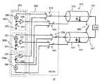
ここで、図1を参照する。図1は、以上に説明した従来技術による測定システム10の概略構成を示す図である。図1において、測定システム10は、測定装置200と、SCUUであるスイッチ装置300とを備える。図1において、少なくとも2つの端子を有する被測定物100は、同軸ケーブル510,520を介して、測定装置200と接続されている。 Reference is now made to FIG. FIG. 1 is a diagram illustrating a schematic configuration of a
測定装置200は、交流信号源210と、直流電流計230,231と、交流電流計260と、レベル可変の直流電圧バイアス源220,250,251と、バッファ240,241とを備える。図中の逆三角形は、グラウンド270,271であり、共通電位、接地またはアースを表している。なお、図1において、参照符号SMUで示される破線枠で囲まれた部分は、被測定物100の電圧電流特性を測定するSMUに対応する部分であることを表している。また、参照符号CMUで示される破線枠で囲まれた部分は、被測定物100の容量対電圧特性を測定するCMUに対応する部分であることを表している。 The
スイッチ装置300は、1極2投スイッチ310,320,330,340を備える。スイッチ310〜340のそれぞれは、1つの共通端子(極、ポール)と、2つの選択端子(投、スロー)とを備える。各スイッチの共通端子には、参照符号cが付されている。また、各スイッチの選択端子は、参照符号aまたはbが付されている。共通端子cは、2つの選択端子(a,b)のいずれか1つと電気的に接続される。スイッチ310の端子aとグラウンド270との間には、電流計230とバイアス源250の直列回路が設けられている。電流計230とバイアス源250との間の電位と同じ電位をスイッチ320の端子aに与えるように、バッファ240が配置されている。スイッチ310の端子bとスイッチ320の端子bとの間には、信号源210とバイアス源220の直列回路が設けられている。スイッチ330の端子aとグラウンド271との間には、電流計231とバイアス源251の直列回路が設けられている。電流計231とバイアス源251との間の電位と同じ電位をスイッチ340の端子aに与えるように、バッファ241が配置されている。スイッチ330の端子bとスイッチ340の端子bとの間には、電流計260が設けられている。また、グラウンド270とグラウンド271は、測定装置200の内部で、電気的に接続されている。 The
同軸ケーブル510,520は、2線同軸ケーブル、すなわち、コアキシャル・ケーブルである。同軸ケーブル510の中心導体511の一端は、スイッチ310の端子cに接続され、中心導体511の他の一端は、被測定物100の一端に接続されている。同軸ケーブル510の外部導体512の一端は、スイッチ320の端子cに接続されている。同軸ケーブル520の中心導体521の一端は、スイッチ330の端子cに接続され、中心導体521の他の一端は、被測定物100の他の一端に接続されている。同軸ケーブル520の外部導体522の一端は、スイッチ340の端子cに接続されている。外部導体512の他の一端および外部導体522の他の一端は、スイッチ400を介して接続されている。外部導体512と外部導体522は、スイッチ400により、選択的に導通する。 The
以上のように説明した構成において、被測定物100の容量対電圧特性を測定する場合には、各スイッチにおいて端子bが選択され、スイッチ400がオンされる。容量対電圧特性を測定するために、交流信号源210が生成する交流信号を被測定物100に印加し、その交流信号に起因して被測定物100に流れる電流を電流計260で測定する。電流260により測定された電流測定値と、交流信号源210が発生する交流信号の周波数および電圧振幅値とに基づき、被測定物100の容量値が求められる。このとき、異なるレベルの複数の直流電圧がバイアス源220で生成され、それらが個々に被測定物100に印加される。そして、バイアス・レベル毎の容量値が取得される。 In the configuration described above, when measuring the capacitance-voltage characteristic of the
また、被測定物100の電圧電流特性を測定する場合には、各スイッチにおいて端子aが選択され、スイッチ400がオフされる。電圧電流特性を測定するために、バイアス源250およびバイアス源251は、被測定物100の端子間に電位差が生じるように、各出力電圧が設定される。そして、それらの出力電圧の差に起因して、被測定物100に流れる電流を電流計230で測定する。 When measuring the voltage-current characteristic of the
ここで、容量対電圧特性の測定後、電圧電流特性の測定へ切り替える際に、その切り替えに伴う待ち時間が問題となっている。例えば、容量対電圧特性を測定する際に、共通線路である同軸ケーブルにDCバイアスが印加され、同軸ケーブルの信号線(中心導体)とガード(外側導体)との間の容量に電荷が蓄積される。電圧電流特性の測定では、この蓄積された電荷が測定誤差となるため、蓄積された電荷が、測定精度上、無視しうる程度に小さくなるまで、電荷の放電を待たねばならない。例えば、共通線路である同軸ケーブルの長さが数メートル程度ある場合に、容量対電圧特性の測定のために当該同軸ケーブルに数十ボルトの直流バイアス電圧を印加した後、1pA程度の測定精度で直流電圧電流特性を測定するとき、数十秒程度の待ち時間が生じ、その長さが問題となっている。 Here, when switching to measurement of voltage-current characteristics after measurement of capacity-to-voltage characteristics, the waiting time associated with the switching is a problem. For example, when measuring capacitance vs. voltage characteristics, a DC bias is applied to a coaxial cable that is a common line, and charges are accumulated in the capacitance between the signal line (center conductor) and the guard (outer conductor) of the coaxial cable. The In the measurement of the voltage-current characteristic, since the accumulated charge becomes a measurement error, it is necessary to wait for the discharge of the charge until the accumulated charge becomes small enough to be ignored for measurement accuracy. For example, when the length of a coaxial cable that is a common line is about several meters, a DC bias voltage of several tens of volts is applied to the coaxial cable for measurement of capacitance vs. voltage characteristics, and the measurement accuracy is about 1 pA. When measuring DC voltage-current characteristics, a waiting time of about several tens of seconds is generated, and the length is a problem.
本発明においては、以下が提供される。すなわち、本第一の発明は、第一の導体と前記第一の導体を囲む第二の導体と前記第二の導体を囲む第三の導体とを具備する同軸線路の前記第一の導体に接続された被測定物の複数種類の電気的特性を、切替装置に接続された第一の測定装置および第二の測定装置を切り替えることにより、測定する方法であって、前記切替装置により前記第一の測定装置が前記被測定物に電気的に接続されている場合に、前記被測定物の第一の電気的特性を測定するための電圧を前記第一の測定装置により前記第一の導体に与えるとともに、前記第一の導体の電位と同じ電位を前記第二の導体に与える第一のステップと、前記切替装置により、前記第一の測定装置を前記被測定物から切り離し、前記第二の測定装置を前記被測定物に電気的に接続する第二のステップと、前記被測定物の第二の電気的特性を前記第二の測定装置により測定する第三のステップと、を含むことを特徴とするものである。 In the present invention, the following is provided. In other words, the first invention provides the first conductor of the coaxial line comprising the first conductor, the second conductor surrounding the first conductor, and the third conductor surrounding the second conductor. A method of measuring a plurality of types of electrical characteristics of a connected object to be measured by switching between a first measuring device and a second measuring device connected to a switching device, wherein When one measuring device is electrically connected to the object to be measured, a voltage for measuring a first electrical characteristic of the object to be measured is applied to the first conductor by the first measuring device. And the first step of applying the same potential to the second conductor to the second conductor and the switching device to separate the first measuring device from the object to be measured. The second measuring device is electrically connected to the object to be measured. Step a, the is characterized in that includes a third step of measuring the second the electrical characteristics of the second measuring device of the object to be measured, a.
また、本第二の発明は、本第一の発明の方法において、前記第三のステップが、前記第一の導体に対するガードとして前記第二の導体を用いて測定することを特徴とするものである。 The second invention is characterized in that, in the method of the first invention, the third step uses the second conductor as a guard for the first conductor. is there.
さらに、本第三の発明は、本第一の発明または本第二の発明の方法において、前記第一のステップが、バッファにより前記第二の導体に電位を与えることを特徴とするものである。 Furthermore, the third invention is characterized in that, in the method of the first invention or the second invention, the first step applies a potential to the second conductor by a buffer. .
またさらに、本第四の発明は、本第一の発明または本第二の発明または本第三の発明の方法において、第一の測定装置が電気容量測定装置であり、第二の測定装置が電圧電流特性測定装置であることを特徴とするものである。 Furthermore, according to the fourth invention, in the method of the first invention, the second invention or the third invention, the first measuring device is a capacitance measuring device, and the second measuring device is It is a voltage-current characteristic measuring device.
また、本第五の発明は、本第一の発明または本第二の発明または本第三の発明または本第四の発明の方法において、前記被測定物が、半導体素子であることを特徴とするものである。 The fifth invention is characterized in that, in the method of the first invention, the second invention, the third invention or the fourth invention, the object to be measured is a semiconductor element. To do.
さらに、本第六の発明は、第一の導体と前記第一の導体を囲む第二の導体と前記第二の導体を囲む第三の導体とを具備する同軸線路の前記第一の導体に接続された被測定物の複数種類の電気的特性を測定するために、第一の測定装置および第二の測定装置のうち選択した一方を前記同軸線路に電気的に接続するスイッチ装置であって、前記第一の測定装置が選択されている場合に、前記第一の測定装置が発生する、前記第一の電気的特性を測定するための電圧を前記第一の導体に与えるように、且つ、前記第一の導体の電位と同じ電位を前記第二の導体に与えるように、前記第一の測定装置を前記同軸線路に電気的に接続し、前記第二の測定装置が選択されている場合に、前記第二の測定装置を少なくとも前記第一の導体および前記第二の導体に電気的に接続することを特徴とするものである。 Furthermore, the sixth invention relates to the first conductor of the coaxial line comprising a first conductor, a second conductor surrounding the first conductor, and a third conductor surrounding the second conductor. A switch device for electrically connecting a selected one of the first measurement device and the second measurement device to the coaxial line in order to measure a plurality of types of electrical characteristics of a connected object to be measured. Applying to the first conductor a voltage for measuring the first electrical characteristic generated by the first measuring device when the first measuring device is selected; and The first measuring device is electrically connected to the coaxial line so that the same potential as the potential of the first conductor is applied to the second conductor, and the second measuring device is selected. In this case, the second measuring device is at least the first conductor and the second conductor. It is characterized in that the electrical connection to.
またさらに、本第六の発明は、本第五の発明の装置において、前記第二の測定装置が選択されている場合に、前記第二の測定装置が前記第二の導体を前記第一の導体に対するガードとして用いることができるように、前記第二の測定装置を前記同軸線路に電気的に接続することを特徴とするものである。 Furthermore, the sixth invention relates to the device according to the fifth invention, wherein when the second measuring device is selected, the second measuring device connects the second conductor to the first conductor. The second measuring device is electrically connected to the coaxial line so that it can be used as a guard for a conductor.
また、本第八の発明は、本第六の発明または本第七の発明の装置において、前記第一の測定装置が選択されている場合に、前記第二の導体に与えられる電位が、バッファを介して与えられることを特徴とするものである In addition, according to the eighth aspect of the invention, in the apparatus of the sixth aspect of the invention or the seventh aspect of the invention, when the first measuring device is selected, the potential applied to the second conductor is a buffer. It is characterized by being given through
さらに、本第九の発明は、本第六の発明または本第七の発明または本第八の発明の装置において、第一の測定装置が電気容量測定装置であり、第二の測定装置が電圧電流特性測定装置であることを特徴とするものである。 Furthermore, the ninth invention is the device of the sixth invention, the seventh invention or the eighth invention, wherein the first measuring device is a capacitance measuring device and the second measuring device is a voltage. It is a current characteristic measuring device.
またさらに、本第十の発明は、本第六の発明または本第七の発明または本第八の発明または本第九の発明の装置において、前記被測定物が、半導体素子であることを特徴とするものである。 Still further, the tenth invention is the apparatus of the sixth invention, the seventh invention, the eighth invention or the ninth invention, wherein the object to be measured is a semiconductor element. It is what.
また、本第十一の発明は、本第六の発明または本第七の発明または本第八の発明または本第九の発明または本第十の発明のスイッチ装置と、前記第一の測定装置および前記第二の測定装置とを備える測定システムである。 The eleventh invention includes the switch device according to the sixth invention, the seventh invention, the eighth invention, the ninth invention, or the tenth invention, and the first measuring device. And a measurement system comprising the second measurement device.
本発明によれば、複数の測定装置を切り替える切替装置と被測定物との間にある信号伝送路における電荷の蓄積、例えば、信号線とガード線との間の容量や、プリント基板上に形成された同軸線路における誘電分極などによる電荷の蓄積を低減もしくは排除することができ、蓄積電荷の放電に起因する測定待ち時間を低減もしくは無くすことができる。また、本発明によれば、複数の測定装置を切り替える切替装置と被測定物との間にある信号伝送路のインピーダンスを、各測定装置に適した個別の異なる値にすることができる。 According to the present invention, charge accumulation in a signal transmission path between a switching device that switches a plurality of measuring devices and an object to be measured, for example, capacitance between a signal line and a guard line, or formation on a printed circuit board Accumulation of charge due to dielectric polarization or the like in the coaxial line thus formed can be reduced or eliminated, and the measurement waiting time due to discharge of the accumulated charge can be reduced or eliminated. Further, according to the present invention, the impedance of the signal transmission path between the switching device for switching a plurality of measuring devices and the device under test can be set to different values suitable for each measuring device.
本発明の実施の形態を、添付の図面を参照しながら、以下に説明する。本発明の実施の形態は、測定システム20である。ここで、図2を参照する。図2において、図1と同一の要素については、同じ参照番号を付して、詳細な説明を省略する。図2は、測定システム20の概略構成を示す図である。図2において、測定システム20は、少なくとも、測定装置200とSCUUであるスイッチ装置700とを備える。測定装置200は、測定装置200と同様に、被測定物100の電圧電流特性および容量対電圧特性を測定する装置である。被測定物100は、少なくとも2つの端子を有する。被測定物100が有する端子のうちの2つの端子が、測定のために、同軸ケーブル910,920を介して、スイッチ装置700と電気的に接続されている。 Embodiments of the present invention will be described below with reference to the accompanying drawings. The embodiment of the present invention is a
スイッチ装置700は、切替装置であるスイッチ710,720,720,740,750,760を備える。スイッチ710〜760のそれぞれは、1つの共通端子と、2つの選択端子とを備える。各スイッチの共通端子には、参照符号cが付されている。また、各スイッチの選択端子は、参照符号aまたはbが付されている。共通端子cは、2つの選択端子(a,b)のいずれか1つと選択的に電気的に接続される。スイッチ710の端子aとグラウンド270との間には、電流計230とバイアス源250の直列回路が設けられている。電流計230とバイアス源250との間の電位と同じ電位をスイッチ720の端子aに与えるように、バッファ240が配置されている。スイッチ730の端子aは、バイアス源250とグラウンド270との間に接続されている。スイッチ710の端子bとスイッチ730の端子bとの間には、信号源210とバイアス源220の直列回路が設けられている。スイッチ720の端子bは、スイッチ710の端子bと接続されている。スイッチ740の端子aとグラウンド271との間には、電流計231とバイアス源251の直列回路が設けられている。電流計231とバイアス源251との間の電位と同じ電位をスイッチ750の端子aに与えるように、バッファ241が配置されている。スイッチ760の端子aは、バイアス源251とグラウンド271との間に接続されている。スイッチ740の端子bとスイッチ760の端子bとの間には、電流計260が設けられている。スイッチ750の端子bは、スイッチ740の端子bと接続されている。 The
同軸ケーブル910,920は、3線同軸ケーブル、すなわち、トライアキシャル・ケーブルである。同軸ケーブル910の一端、すなわち、スイッチ装置700側において、中心導体911がスイッチ710の端子cに、内部導体912がスイッチ720の端子cに、外部導体913がスイッチ730の端子cに、それぞれ接続されている。同軸ケーブル910の他の一端、すなわち、被測定物100側において、中心導体911が被測定物100に接続され、内部導体912が開放されている。同軸ケーブル920の一端、すなわち、スイッチ装置700側において、中心導体921がスイッチ740の端子c、内部導体922がスイッチ750の端子cに、外部導体923がスイッチ760の端子cに、それぞれ接続されている。同軸ケーブル910の他の一端、すなわち、被測定物100側において、中心導体921が被測定物100に接続され、内部導体922が開放されている。同軸ケーブル910および920の他の一端において、外部導体923が外部導体913と接続されている。 The
以上に説明した構成において、被測定物100の容量対電圧特性は、以下の手順で測定される。まず、各スイッチにおいて端子bを選択する。次に、交流信号源210が生成する交流信号を被測定物100に印加し、その交流信号に起因して被測定物100に流れる電流を電流計260で測定する。次に、電流計260により測定された電流測定値と、交流信号源210が発生する交流信号の周波数および電圧振幅値とに基づき、被測定物100の容量値を算出する。また、上記の容量測定過程において、必要に応じて、異なるレベルの複数の直流電圧をバイアス源220で生成し、それらを個々に被測定物100に印加する。そして、バイアス・レベル毎の容量値を測定する。 In the configuration described above, the capacity-voltage characteristic of the
また、被測定物100の電圧電流特性は、以下の手順で測定される。まず、各スイッチにおいて端子aを選択する。次に、被測定物100の端子間に電位差が生じるように、バイアス源250およびバイアス源251の各出力電圧を設定する。次に、それらの出力電圧の差に起因して、被測定物100に流れる電流を電流計230で測定する。また、上記の電流測定過程において、必要に応じて、異なるレベルの複数の電位差が被測定物100の端子間に生じるように、バイアス源250およびバイアス源251の各出力電圧を設定する。そして、電位差レベル毎に、被測定物100に流れる電流を電流計230で測定する。 Moreover, the voltage-current characteristic of the
容量対電圧特性の測定では、例えば、スイッチ710の端子bとスイッチ710の端子bが同電位であるので、中心導体911と内部導体912との電位差は、実質的にゼロとなるか、無視しうるレベルとなる。従って、中心導体911と内部導体912との間に蓄積される電荷も、実質的にゼロであるか、無視しうる量となる。この結果、容量対電圧特性の測定後に、電圧電流特性の測定を実施する場合に、トライアキシャル・ケーブル910,920に蓄積された電荷の放出を待つ必要がない。また、当該電荷が電圧電流特性の測定結果に影響を及ぼす心配もない。 In the measurement of the capacitance-voltage characteristic, for example, since the terminal b of the
さて、上記の実施形態において、電流計260の両端電位差が実質的にゼロである場合には、スイッチ740〜760および同軸ケーブル920を、スイッチ330〜340および同軸ケーブル520およびスイッチ400と置き換えても良い。この場合、スイッチ740〜760およびスイッチ400に係る接続や動作は、前述のとおりである。例えば、置き換えられるスイッチ400は、同軸ケーブルの外部導体間に接続される。 In the above embodiment, if the potential difference across the
また、上記の実施形態において、スイッチ720の端子bがスイッチ710の端子bに、スイッチ750の端子bがスイッチ740の端子bに、それぞれ接続されている。この表現は、説明の便宜のためのものであり、本発明の技術的思想がこれに限定されるべきではない。重要なことは、スイッチ710の端子bの電位と同じ電位をスイッチ720の端子bに、スイッチ740の端子bの電位と同じ電位をスイッチ750の端子bに、与えることにある。従って、例えば、スイッチ720の端子bがスイッチ710の端子bにバッファを介して接続され、スイッチ750の端子bがスイッチ740の端子bにバッファを介して接続されるようにしても良い。この場合、アクティブガードとしての機能が追加され、それによる測定精度の改善が見込まれる。 In the above embodiment, the terminal b of the
さらに、上記の実施形態において、同軸ケーブル910,920は、スイッチ装置700とは独立したものとして表現されている。この表現は、説明の便宜のためのものであり、本発明の技術的思想がこれに限定されるべきではない。重要なことは、スイッチ710〜760から被測定物100までの区間が、できるだけトライアキシャル構造を有することにある。従って、その区間に該当する限り、例えば、スイッチ装置700の内の信号伝送路も同軸構造を有することが望ましく、そのような態様も本発明の一態様である。 Further, in the above-described embodiment, the
またさらに、上記の実施形態において、スイッチ730およびスイッチ760を1極1投スイッチに置き換えることもできる。言い換えれば、スイッチ730およびスイッチ760から、それぞれの端子aを除外することもできる。その場合、外部導体913とバイアス源220とを選択的に接続するように、かつ、外部導体923と電流計260とを選択的に接続するように、1極1投スイッチが配置される。 Furthermore, in the above embodiment, the
次に、より詳細な本発明の実施例について説明する。ここで、図3を参照する。図3は、本発明の実施例である半導体測定システム30の構成を示す図である。半導体測定システム30は、測定装置1000と接続装置2000とを備える。測定装置1000は、SMU1100と、SMU1200と、CMU1300とを備える。SMU1100、SMU1200、およびCMU1300は、測定装置1000もしくは測定装置1000に接続された制御装置により、制御される。 Next, more detailed examples of the present invention will be described. Reference is now made to FIG. FIG. 3 is a diagram showing a configuration of a
SMU1100,1200は、それぞれ、直流の電圧源、電流源、電圧計、電流計を具備し、それらを任意に組み合わせて測定する装置である。また、SMU1100,1200は、個々に測定することができるし、それらが協働して測定することもできる。SMU1100は、ケルビン接続のために、センス端子S1およびフォース端子F1を備える。また、SMU1200は、ケルビン接続のために、センス端子S2およびフォース端子F2を備える。端子S1,F1,S2,F2のそれぞれは、トライアキシャル構造(3線同軸構造)を有する。すなわち、端子S1,F1,S2,F2のそれぞれは、中心導体と、中心導体を囲む内部導体と、内部導体を囲む外部導体とを備える。端子S1,F1,S2,F2のそれぞれにおいて、中心導体には信号が伝達され、外側シールド導体は筐体グラウンドに接続され、中心導体と外側シールド導体との間にあるガード導体には中心導体の信号と同電位に保たれたガード信号が伝達される。 Each of the
CMU1300は、容量、インダクタンスおよび抵抗などのインピーダンスを測定する装置である。CMU1300は、High側の電流を出力するための端子Hcと、High側の電圧を測定するための端子Hpと、Low側の電圧を測定するための端子Lpと、Low側の電流を出力するための端子Lcとを備える。端子Hc,Hp,Lp,Lcは、それぞれコアキシャル構造(2線同軸構造)を有する。すなわち、端子Hc,Hp,Lp,Lcのそれぞれは、中心導体と、中心導体を囲む外部導体とを備える。各端子において、中心導体には信号が伝達され、シールドである外部導体は筐体グラウンドからフローティングされている。CMU1300は、接続装置2000を制御するためのコントローラ1310を備える。コントローラ1310の制御出力は、端子1311に供給される。なお、コントローラ1310は、測定装置1000に備えられてもよい。 The
被測定物110は、例えば、集積回路製造プロセスの最適条件を判定するためにシリコンウエハー上に設けられるTEG(Test Element Group)領域に形成される半導体素子や、トランジスタやキャパシタなどの個別素子である。図において、被測定物110は、トライアキシャル・ケーブル5000および5010により、被測定物110が備える端子のうちの2つの端子が接続装置2000と接続されている。なお、必要に応じて、被測定物110と接続装置2000との間には、プローブ装置や、スイッチング・マトリックスが配置される。 The device under
トライアキシャル・ケーブル5000および5010は、被測定物110側の端部において、それぞれの中心導体が被測定物110に接続され、それぞれの外部導体が電気的に接続され、それぞれの内部導体が開放されている。
接続装置2000は、端子S1を接続するための端子2100、端子F1を接続するための端子2110、端子S2を接続するための端子2200、および、端子F2を接続するための端子2210を備える。また、接続装置2000は、端子Hcを接続するための端子2300、端子Hpを接続するための端子2310、端子Lpを接続するための端子2320、端子Lcを接続するための端子2330を備える。さらに、接続装置2000は、被測定物110を接続するための端子2500,2510を備える。端子2100,2110,2200,2210,2500,2510は、それぞれ、トライアキシャル構造を有する。また、端子2300,2310,2320,2330は、それぞれ、コアキシャル構造を有する。さらに、対応する端子同士は、接続3000により接続されている。なお、接続3000は、直接的接続でも良いし、ケーブルなどを介した接続、すなわち、間接的接続でも良い。 The
ここで、図4を参照する。図4は、接続装置2000の内部構造を示す図である。図4において、接続装置2000は、切替装置であるスイッチ群T1,T2,T3,T4を備える。各スイッチ群において、個々のスイッチは、1極1投スイッチである。また、各スイッチ群において、個々のスイッチは、それぞれに付されたa〜cの参照記号により区別される。例えば、スイッチ群T1の上側のスイッチは、T1aとして認識される。また、例えば、スイッチ群T4の中央のスイッチは、T4bとして認識される。 Reference is now made to FIG. FIG. 4 is a diagram showing an internal structure of the
端子2100および端子2110の中心導体は、スイッチT1bを介して、端子2500の中心導体に選択的に接続される。端子2110の内部導体は、スイッチT1aを介して、端子2500の内部導体に選択的に接続される。端子2100および端子2110の外部導体は、筐体グラウンドに接続されている。 The center conductors of the
端子2200および端子2210の中心導体は、スイッチT2bを介して、端子2510の中心導体に選択的に接続される。端子2210の内部導体は、スイッチT2aを介して、端子2510の内部導体に選択的に接続される。端子2200および端子2210の外部導体は、筐体グラウンドに接続されている。 The center conductors of the terminal 2200 and the terminal 2210 are selectively connected to the center conductor of the terminal 2510 via the switch T2b. The inner conductor of the terminal 2210 is selectively connected to the inner conductor of the terminal 2510 via the switch T2a. The external conductors of the terminal 2200 and the terminal 2210 are connected to the housing ground.
端子2300および端子2310の中心導体は、スイッチT3bおよびスイッチT3cを介して、端子2500の中心導体および内部導体に選択的に接続される。端子2300および端子2310の外部導体は、スイッチT3aを介して、端子2500の外部導体に選択的に接続される。端子2330および端子2340の中心導体は、スイッチT4bおよびスイッチT4cを介して、端子2510の中心導体および内部導体に選択的に接続される。端子2330および端子2340の外部導体は、スイッチT4aを介して、端子2510の外部導体に選択的に接続される。なお、端子2300,2310,2320,2340の外部導体は、それ自身、筐体グラウンドからフローティングされている。 The center conductors of the terminal 2300 and the terminal 2310 are selectively connected to the center conductor and the inner conductor of the terminal 2500 via the switch T3b and the switch T3c. The external conductors of the terminal 2300 and the terminal 2310 are selectively connected to the external conductor of the terminal 2500 via the switch T3a. The center conductors of
端子2500および端子2510の外部導体は、筐体グラウンドに接続されている。 The outer conductors of the terminal 2500 and the terminal 2510 are connected to the housing ground.
なお、特に図では示していないが、スイッチ群T1およびT3と端子2500との間の信号伝送路、および、スイッチ群T2およびT4と端子2510との間の信号伝送路は、設計が許す限り、トライアキシャル構造を有する。それらトライアキシャル構造を有する信号伝送路は、エッチング処理によりプリント基板に形成された信号線パターンや、同軸ケーブルなどで構成される。 Although not specifically shown in the figure, the signal transmission path between the switch groups T1 and T3 and the terminal 2500 and the signal transmission path between the switch groups T2 and T4 and the terminal 2510 are as long as the design permits. It has a triaxial structure. The signal transmission path having the triaxial structure is configured by a signal line pattern formed on the printed circuit board by an etching process, a coaxial cable, or the like.
スイッチ群T1は、端子2100および端子2110を、端子2500に選択的に接続する。スイッチ群T2は、端子2200および端子2210を、端子2510に選択的に接続する。スイッチ群T3は、端子2300および端子2310を、端子2500に選択的に接続する。スイッチ群T4は、端子2330および端子2340を、端子2510に選択的に接続する。スイッチ群T1,T2,T3,T4は、コントローラ2200の制御により、次の2状態のいずれかになる。あるときは、スイッチ群T1およびスイッチ群T2の各スイッチはオンであり、スイッチ群T3およびスイッチ群T4の各スイッチはオフである。また、あるときは、スイッチ群T1およびスイッチ群T2の各スイッチはオフであり、スイッチ群T3およびスイッチ群T4の各スイッチはオンである。コントローラ2200自身は、端子2400を介して受信する制御情報に応じて動作する。 The switch group T1 selectively connects the terminal 2100 and the terminal 2110 to the
以上に説明した半導体測定システム30において、被測定物110の容量対電圧特性を測定する場合、スイッチ群T1およびT2をオンにし、スイッチ群T3およびT4をオフにする。その後の測定手順は、上記の実施態様で説明したとおりである。また、被測定物110の電圧電流特性を測定する場合、スイッチ群T1およびT2をオフにし、スイッチ群T3およびT4をオンにする。その後の測定手順は、上記の実施態様で説明したとおりである。 In the
容量対電圧特性の測定では、被測定物110に接続されているトライアキシャル構造の信号伝送路において、中心導体および内部導体の電位が同一となる。従って、上記の実施態様で説明したとおり、容量対電圧特性の測定後に、電圧電流特性の測定を実施する場合に、切替装置である各スイッチ群と被測定物110との間の信号伝送路に蓄積された電荷の放出を待つ必要がない。また、当該電荷が電圧電流特性の測定結果に影響を及ぼす心配もない。 In the measurement of the capacitance-voltage characteristic, the potentials of the center conductor and the inner conductor are the same in the triaxial structure signal transmission path connected to the device under
上記の実施例において、切替装置である各スイッチ群と被測定物110との間の信号伝送路において、SMUが使用する線路の特性インピーダンスとCMUが使用する線路の特性インピーダンスは、共通の値であっても良いし、異なる値であっても良い。例えば、SMUが使用する線路の特性インピーダンスは、容量地が小さいほど良く、その結果、特性インピーダンスは大きいほど良い。従って、例えば、各スイッチ群と被測定物110との間のトライアキシャル信号伝送路において、中心導体と内部導体とで構成される線路の特性インピーダンスを1キロオームとし、内部導体と外部導体とで構成される線路の特性インピーダンスを50オームとすると、測定精度上、好都合である。 In the above embodiment, the characteristic impedance of the line used by the SMU and the characteristic impedance of the line used by the CMU are common values in the signal transmission path between each switch group serving as the switching device and the
10,20 測定システム
30 半導体測定システム
100,110 被測定物
200 測定装置
210,210 交流信号源
220,250,251 , 直流電圧バイアス源
230,231 直流電流計
260 交流電流計
240,241 バッファ
270,271 グラウンド
300,700 スイッチ装置
310,320,330,340,400 スイッチ
510,520 同軸ケーブル
511,521 中心導体
512,522 外部導体
710,720,730,740,750,760 スイッチ
910,920 トライアキシャル・ケーブル
911,921 中心導体
912,922 内部導体
913,923 外部導体
1000 測定装置
1310,2200 コントローラ
1311 端子
2000 接続装置
2100,2110,2200,2210 端子
2300,2310,2320,2330 端子
2400,2500,2510 端子
3000 接続
5000,5010 トライアキシャル・ケーブル
10, 20
Claims (11)
Translated fromJapanese前記切替装置により前記第一の測定装置が前記被測定物に電気的に接続されている場合に、前記被測定物の第一の電気的特性を測定するための電圧を前記第一の測定装置により前記第一の導体に与えるとともに、前記第一の導体の電位と同じ電位を前記第二の導体に与える第一のステップと、
前記切替装置により、前記第一の測定装置を前記被測定物から切り離し、前記第二の測定装置を前記被測定物に電気的に接続する第二のステップと、
前記被測定物の第二の電気的特性を前記第二の測定装置により測定する第三のステップと、
を含むことを特徴とする測定方法。Plural types of objects to be measured connected to the first conductor of the coaxial line, the first conductor, the second conductor surrounding the first conductor, and the third conductor surrounding the second conductor. A method of measuring the electrical characteristics of the first measuring device and the second measuring device connected to the switching device,
When the first measuring device is electrically connected to the device under test by the switching device, a voltage for measuring the first electrical characteristic of the device under test is supplied to the first measuring device. The first step of applying to the first conductor and applying the same potential to the second conductor as the potential of the first conductor;
A second step of disconnecting the first measuring device from the device under test by the switching device and electrically connecting the second measuring device to the device under test;
A third step of measuring a second electrical characteristic of the object to be measured by the second measuring device;
A measurement method comprising:
前記第一の測定装置が選択されている場合に、前記第一の測定装置が発生する、前記第一の電気的特性を測定するための電圧を前記第一の導体に与えるように、且つ、前記第一の導体の電位と同じ電位を前記第二の導体に与えるように、前記第一の測定装置を前記同軸線路に電気的に接続し、
前記第二の測定装置が選択されている場合に、前記第二の測定装置を少なくとも前記第一の導体および前記第二の導体に電気的に接続する、
ことを特徴とするスイッチ装置。A plurality of types of objects to be measured connected to the first conductor of the coaxial line, comprising a first conductor, a second conductor surrounding the first conductor, and a third conductor surrounding the second conductor A switching device for electrically connecting a selected one of the first measuring device and the second measuring device to the coaxial line,
Applying to the first conductor a voltage for measuring the first electrical characteristic generated by the first measuring device when the first measuring device is selected; and Electrically connecting the first measuring device to the coaxial line so as to give the second conductor the same potential as the potential of the first conductor;
Electrically connecting the second measuring device to at least the first conductor and the second conductor when the second measuring device is selected;
A switch device characterized by that.
A measurement system comprising the switch device according to any one of claims 6 to 10, the first measurement device, and the second measurement device.
Priority Applications (1)
| Application Number | Priority Date | Filing Date | Title |
|---|---|---|---|
| JP2006290803AJP2008107216A (en) | 2006-10-26 | 2006-10-26 | Measurement method, switch device, and measurement system including the switch device |
Applications Claiming Priority (1)
| Application Number | Priority Date | Filing Date | Title |
|---|---|---|---|
| JP2006290803AJP2008107216A (en) | 2006-10-26 | 2006-10-26 | Measurement method, switch device, and measurement system including the switch device |
Publications (1)
| Publication Number | Publication Date |
|---|---|
| JP2008107216Atrue JP2008107216A (en) | 2008-05-08 |
Family
ID=39440682
Family Applications (1)
| Application Number | Title | Priority Date | Filing Date |
|---|---|---|---|
| JP2006290803APendingJP2008107216A (en) | 2006-10-26 | 2006-10-26 | Measurement method, switch device, and measurement system including the switch device |
Country Status (1)
| Country | Link |
|---|---|
| JP (1) | JP2008107216A (en) |
Cited By (7)
| Publication number | Priority date | Publication date | Assignee | Title |
|---|---|---|---|---|
| JP2013096998A (en)* | 2011-11-04 | 2013-05-20 | Keithley Instruments Inc | Dc-ac probe card |
| CN106018971A (en)* | 2016-05-04 | 2016-10-12 | 常州工学院 | Multifunctional capacitance apparatus used for wheat leaf physiological electrical characteristic determination |
| CN106053950A (en)* | 2016-05-04 | 2016-10-26 | 常州工学院 | Capacitor device used for measuring physiological dielectric characteristic of wheat leaf |
| JP2017049148A (en)* | 2015-09-02 | 2017-03-09 | 株式会社クオルテック | Measuring system and measuring method |
| CN105759126B (en)* | 2016-05-04 | 2018-09-28 | 常州工学院 | A kind of reinforcement type is used for the capacitive means of wheat leaf blade Physiological Electrical Characteristics measurement |
| US10228362B2 (en) | 2014-11-28 | 2019-03-12 | Advantest Corporation | Measurement apparatus |
| US10436822B2 (en) | 2014-11-28 | 2019-10-08 | Advantest Corporation | Measurement apparatus |
- 2006
- 2006-10-26JPJP2006290803Apatent/JP2008107216A/enactivePending
Cited By (8)
| Publication number | Priority date | Publication date | Assignee | Title |
|---|---|---|---|---|
| JP2013096998A (en)* | 2011-11-04 | 2013-05-20 | Keithley Instruments Inc | Dc-ac probe card |
| CN103116045B (en)* | 2011-11-04 | 2020-01-31 | 基思利仪器公司 | DC-AC probe card topology |
| US10228362B2 (en) | 2014-11-28 | 2019-03-12 | Advantest Corporation | Measurement apparatus |
| US10436822B2 (en) | 2014-11-28 | 2019-10-08 | Advantest Corporation | Measurement apparatus |
| JP2017049148A (en)* | 2015-09-02 | 2017-03-09 | 株式会社クオルテック | Measuring system and measuring method |
| CN106018971A (en)* | 2016-05-04 | 2016-10-12 | 常州工学院 | Multifunctional capacitance apparatus used for wheat leaf physiological electrical characteristic determination |
| CN106053950A (en)* | 2016-05-04 | 2016-10-26 | 常州工学院 | Capacitor device used for measuring physiological dielectric characteristic of wheat leaf |
| CN105759126B (en)* | 2016-05-04 | 2018-09-28 | 常州工学院 | A kind of reinforcement type is used for the capacitive means of wheat leaf blade Physiological Electrical Characteristics measurement |
Similar Documents
| Publication | Publication Date | Title |
|---|---|---|
| US6998869B2 (en) | Semiconductor device characteristics measurement apparatus and connection apparatus | |
| US6791344B2 (en) | System for and method of testing a microelectronic device using a dual probe technique | |
| US7924035B2 (en) | Probe card assembly for electronic device testing with DC test resource sharing | |
| US5861743A (en) | Hybrid scanner for use in an improved MDA tester | |
| US7262626B2 (en) | Connection apparatus and cable assembly for semiconductor-device characteristic measurement apparatus | |
| US8872534B2 (en) | Method and apparatus for testing devices using serially controlled intelligent switches | |
| US20080303541A1 (en) | Method and Apparatus For Increasing Operating Frequency Of A System For Testing Electronic Devices | |
| JP2008107216A (en) | Measurement method, switch device, and measurement system including the switch device | |
| JPH07218544A (en) | Probe device | |
| KR20070074606A (en) | Interface device for semiconductor device tester | |
| US20130082731A1 (en) | Switching matrix and testing system for semiconductor characteristic measurement using the same | |
| JPH10239372A (en) | Substrate inspection instrument and substrate inspection method | |
| US7535243B2 (en) | Method and program for controlling an apparatus for measurement of characteristics of a semiconductor device under test | |
| US5760596A (en) | Testing series passive components without contacting the driven node | |
| KR20120005941A (en) | Probe unit and circuit board inspection device for circuit board inspection | |
| JP3558425B2 (en) | Signal switching device and switch circuit | |
| JPH11264853A (en) | Contact test device and semiconductor test device | |
| JP3053012B2 (en) | Test circuit and test method for semiconductor device | |
| JP2013024729A (en) | Electric length measuring method in semiconductor testing device | |
| JPH10213616A (en) | Liquid crystal driving integrated circuit and test method thereof | |
| JPH1048289A (en) | Semiconductor integrated circuit test system | |
| JPS6384131A (en) | Device for inspecting semiconductor device | |
| JPH04111334A (en) | Semiconductor device |