JP2008103688A - Location of phosphor in light-emitting diode - Google Patents
Location of phosphor in light-emitting diodeDownload PDFInfo
- Publication number
- JP2008103688A JP2008103688AJP2007216808AJP2007216808AJP2008103688AJP 2008103688 AJP2008103688 AJP 2008103688AJP 2007216808 AJP2007216808 AJP 2007216808AJP 2007216808 AJP2007216808 AJP 2007216808AJP 2008103688 AJP2008103688 AJP 2008103688A
- Authority
- JP
- Japan
- Prior art keywords
- resin
- temperature
- phosphor
- led lamp
- package
- Prior art date
- Legal status (The legal status is an assumption and is not a legal conclusion. Google has not performed a legal analysis and makes no representation as to the accuracy of the status listed.)
- Granted
Links
Images

Classifications
- H—ELECTRICITY
- H10—SEMICONDUCTOR DEVICES; ELECTRIC SOLID-STATE DEVICES NOT OTHERWISE PROVIDED FOR
- H10H—INORGANIC LIGHT-EMITTING SEMICONDUCTOR DEVICES HAVING POTENTIAL BARRIERS
- H10H20/00—Individual inorganic light-emitting semiconductor devices having potential barriers, e.g. light-emitting diodes [LED]
- H10H20/80—Constructional details
- H10H20/85—Packages
- H10H20/855—Optical field-shaping means, e.g. lenses
- H10H20/856—Reflecting means
- H—ELECTRICITY
- H10—SEMICONDUCTOR DEVICES; ELECTRIC SOLID-STATE DEVICES NOT OTHERWISE PROVIDED FOR
- H10H—INORGANIC LIGHT-EMITTING SEMICONDUCTOR DEVICES HAVING POTENTIAL BARRIERS
- H10H20/00—Individual inorganic light-emitting semiconductor devices having potential barriers, e.g. light-emitting diodes [LED]
- H10H20/80—Constructional details
- H10H20/85—Packages
- H10H20/852—Encapsulations
- H10H20/853—Encapsulations characterised by their shape
- H—ELECTRICITY
- H01—ELECTRIC ELEMENTS
- H01L—SEMICONDUCTOR DEVICES NOT COVERED BY CLASS H10
- H01L2224/00—Indexing scheme for arrangements for connecting or disconnecting semiconductor or solid-state bodies and methods related thereto as covered by H01L24/00
- H01L2224/01—Means for bonding being attached to, or being formed on, the surface to be connected, e.g. chip-to-package, die-attach, "first-level" interconnects; Manufacturing methods related thereto
- H01L2224/42—Wire connectors; Manufacturing methods related thereto
- H01L2224/47—Structure, shape, material or disposition of the wire connectors after the connecting process
- H01L2224/48—Structure, shape, material or disposition of the wire connectors after the connecting process of an individual wire connector
- H01L2224/4805—Shape
- H01L2224/4809—Loop shape
- H01L2224/48091—Arched
- H—ELECTRICITY
- H01—ELECTRIC ELEMENTS
- H01L—SEMICONDUCTOR DEVICES NOT COVERED BY CLASS H10
- H01L2224/00—Indexing scheme for arrangements for connecting or disconnecting semiconductor or solid-state bodies and methods related thereto as covered by H01L24/00
- H01L2224/01—Means for bonding being attached to, or being formed on, the surface to be connected, e.g. chip-to-package, die-attach, "first-level" interconnects; Manufacturing methods related thereto
- H01L2224/42—Wire connectors; Manufacturing methods related thereto
- H01L2224/47—Structure, shape, material or disposition of the wire connectors after the connecting process
- H01L2224/48—Structure, shape, material or disposition of the wire connectors after the connecting process of an individual wire connector
- H01L2224/484—Connecting portions
- H01L2224/48463—Connecting portions the connecting portion on the bonding area of the semiconductor or solid-state body being a ball bond
- H01L2224/48465—Connecting portions the connecting portion on the bonding area of the semiconductor or solid-state body being a ball bond the other connecting portion not on the bonding area being a wedge bond, i.e. ball-to-wedge, regular stitch
- H—ELECTRICITY
- H10—SEMICONDUCTOR DEVICES; ELECTRIC SOLID-STATE DEVICES NOT OTHERWISE PROVIDED FOR
- H10H—INORGANIC LIGHT-EMITTING SEMICONDUCTOR DEVICES HAVING POTENTIAL BARRIERS
- H10H20/00—Individual inorganic light-emitting semiconductor devices having potential barriers, e.g. light-emitting diodes [LED]
- H10H20/80—Constructional details
- H10H20/85—Packages
- H10H20/8506—Containers
- H—ELECTRICITY
- H10—SEMICONDUCTOR DEVICES; ELECTRIC SOLID-STATE DEVICES NOT OTHERWISE PROVIDED FOR
- H10H—INORGANIC LIGHT-EMITTING SEMICONDUCTOR DEVICES HAVING POTENTIAL BARRIERS
- H10H20/00—Individual inorganic light-emitting semiconductor devices having potential barriers, e.g. light-emitting diodes [LED]
- H10H20/80—Constructional details
- H10H20/85—Packages
- H10H20/851—Wavelength conversion means
- H10H20/8516—Wavelength conversion means having a non-uniform spatial arrangement or non-uniform concentration, e.g. patterned wavelength conversion layer or wavelength conversion layer with a concentration gradient
Landscapes
- Led Device Packages (AREA)
- Luminescent Compositions (AREA)
Abstract
Translated fromJapaneseDescription
Translated fromJapanese 本発明は、色変換、色混合又はその両方の目的を果たすために蛍光体を組み込む発光ダイオードの製造及び構造における改善に関する。
本出願は、2006年9月1日に出願された仮特許出願第60/824,385号からの優先権を主張する。The present invention relates to improvements in the fabrication and construction of light emitting diodes that incorporate phosphors to serve the purpose of color conversion, color mixing, or both.
This application claims priority from provisional patent application No. 60 / 824,385, filed Sep. 1, 2006.
発光ダイオード(LED)は半導体デバイスの一種であり、電流がp−n接合を通過するときに光子を生成する。その基本構造において、発光ダイオードは、少なくとも1つのp型層及び1つのn型層を含み、それらの層は合わせて接合部を画定する。接合部を横断する電流が注入されるとき、電子及び正孔が再結合し、光子を生成することができる。電子工学及び物理学の十分に理解されている原理によれば、光子の波長(それゆえ周波数)は、再結合のエネルギー変化に基づく。さらに、そのエネルギーは、半導体材料のバンドギャップ、すなわち材料の価電子帯と伝導帯との間のエネルギー差によって規定又は抑制される。 Light emitting diodes (LEDs) are a type of semiconductor device that generate photons when current passes through a pn junction. In its basic structure, the light emitting diode includes at least one p-type layer and one n-type layer, which together define a junction. When current across the junction is injected, electrons and holes can recombine and generate photons. According to well-understood principles of electronics and physics, the photon wavelength (and hence the frequency) is based on the recombination energy change. Furthermore, the energy is defined or suppressed by the band gap of the semiconductor material, i.e. the energy difference between the valence band and the conduction band of the material.
結果として、LEDによって放射される色は、そのLEDが形成される材料によって実質的に決定される。ガリウムヒ素(GaAs)及びガリウムリン(GaP)から形成されるダイオードは、可視スペクトルの低い方のエネルギーである赤色部分及び黄色部分において光子を発する傾向がある。炭化シリコン(SiC)及び第III族窒化物のような材料は、さらに広いバンドギャップを有し、それゆえ、可視スペクトルの緑色部分、青色部分及び紫色部分において、並びに電磁スペクトルの紫外線部分において現われる、さらにエネルギーが高い光子を生成することができる。 As a result, the color emitted by an LED is substantially determined by the material from which the LED is formed. Diodes formed from gallium arsenide (GaAs) and gallium phosphide (GaP) tend to emit photons in the red and yellow portions, which are the lower energies of the visible spectrum. Materials such as silicon carbide (SiC) and Group III nitrides have wider band gaps and therefore appear in the green, blue and violet portions of the visible spectrum and in the ultraviolet portion of the electromagnetic spectrum. Furthermore, photons with higher energy can be generated.
応用形態によっては、その出力が加減されるか、又は異なる色に変換されるときに、LEDの有用性が高くなることがある。詳細には、青色発光LEDの利用可能性が大幅に増えたことで、青色光子を変換する黄色発光蛍光体の使用量も同じく増えている。具体的には、ダイオードが発光する青色光と、蛍光体が発光する黄色光とを組み合わせると、白色光を生成することができる。固体源からの白色光を利用できるようになると、特に照明を含む多数の応用形態で、及びカラーディスプレイのためのバックライトとして、それらの固体源を組み込むことができるようになる。そのようなデバイス(たとえば、フラットコンピュータ画面、携帯情報端末及び携帯電話)では、青色LED及び黄色蛍光体によって白色光を生成し、その後、カラー素子(多くの場合に、液晶、「LCD」によって形成される)を照明するために、その白色光を何らかの方法で行き渡らせる。 Depending on the application, the usefulness of the LED may increase when its output is moderated or converted to a different color. Specifically, the availability of blue light emitting LEDs has increased significantly, so the amount of yellow light emitting phosphor that converts blue photons is also increasing. Specifically, white light can be generated by combining blue light emitted from a diode and yellow light emitted from a phosphor. When white light from solid sources becomes available, it becomes possible to incorporate those solid sources in many applications, particularly including illumination, and as a backlight for color displays. In such devices (eg flat computer screens, personal digital assistants and mobile phones), white light is generated by blue LEDs and yellow phosphors, and then formed by color elements (often liquid crystals, “LCD”) To illuminate the white light in some way.
本出願では、用語「白色光」は一般的な意味において用いられる。色の発生及び人間の目による色の知覚に精通する人であれば、正確を期すために、ある特定の周波数混合を「白色」と定義することができることは理解されよう。本明細書において説明されるダイオードのうちのいくつかは、そのような正確な出力を生成することができるが、本明細書では、用語「白色」は、それよりも幾分広く用いられ、種々の人又は検出器が、たとえばわずかに黄色みがかっているか、又は青みがかっているものと知覚することになる光を含む。 In this application, the term “white light” is used in a general sense. One skilled in the art of color generation and color perception by the human eye will understand that a particular frequency mixture can be defined as “white” for accuracy. Although some of the diodes described herein can produce such an accurate output, in this specification the term “white” is used somewhat more broadly, and various The person or detector, for example, will perceive light that will be perceived as slightly yellowish or bluish.
LEDと共に用いられる蛍光体の多くは、LEDチップに隣接して配置される、蛍光組成物から成る細かい粒子である。最も典型的な例では、LEDチップは、回路基板又は他の電気的接続(たとえば、リードフレーム)上に実装され、レンズを形成する実質的に透明な材料によって封入される。最も典型的には、レンズはポリマーであり、大抵の場合には、エポキシ又はシリコーンである。蛍光体が組み込まれるとき、典型的には、樹脂内の懸濁物として導入される。その後、その懸濁物はLEDに被着し、硬化する。結果として形成されるパッケージ(チップ、電気リード、レンズ)は、LEDランプと呼ばれる。 Many of the phosphors used with LEDs are fine particles of a phosphor composition that are placed adjacent to the LED chip. In the most typical example, the LED chip is mounted on a circuit board or other electrical connection (eg, a lead frame) and encapsulated by a substantially transparent material that forms a lens. Most typically, the lens is a polymer, most often an epoxy or silicone. When the phosphor is incorporated, it is typically introduced as a suspension within the resin. The suspension is then applied to the LED and cured. The resulting package (chip, electrical lead, lens) is called an LED lamp.
蛍光体は粒子から構成され、樹脂の中に分散されるので、LEDチップに対するその物理的な位置は、LEDの効率及び出力に影響を及ぼす可能性がある。樹脂内の蛍光体粒子の分布を厳密に制御することができない場合、結果として形成されるLEDランプでは、その出力が、他の状況において、その物理的及び電子工学的特性が与えることができる出力よりも劣化するという不都合が生じることがある。 Since the phosphor is composed of particles and dispersed in the resin, its physical position with respect to the LED chip can affect the efficiency and output of the LED. If the distribution of the phosphor particles in the resin cannot be strictly controlled, the resulting LED lamp has an output that can be given its physical and electronic properties in other situations. Inconvenience of deterioration may occur.
黄色蛍光体と共に青色LEDを用いることが増えてくるにつれて、青色及びそれよりも高いエネルギーの光子に露光されるときに、多数のエポキシ樹脂を含む特定の樹脂が、他の樹脂よりも容易に光化学反応する傾向がある(残念なことに、大部分の場合に結果として劣化する)ために、そのような高いエネルギーのデバイスには適していないことが明らかになっている。 As the use of blue LEDs with yellow phosphors increases, certain resins, including many epoxy resins, are easier to photochemically than other resins when exposed to blue and higher energy photons. It has proved unsuitable for such high energy devices because of its tendency to react (unfortunately resulting in degradation in most cases).
別の要因として、蛍光体粒子をポリマー樹脂に加えて、その後、蛍光体を含む樹脂をLEDチップに被着するには、一連の製造ステップを必要とする。一般的に言うと、その樹脂は、所望のパッケージ形状に成型されるか、又は別の方法で形作られることができるように、液状で調製されなければならない。さらに、その蛍光体は、パッケージに組み込むことができるように、そのような液状で樹脂と機械的に混合されなければならない。実際に製造するために、その樹脂は、適当な「ポットライフ」、すなわち硬化し始める前に良好に機能することができる時間間隔を持つべきである。 As another factor, adding phosphor particles to a polymer resin and then depositing the resin containing the phosphor on the LED chip requires a series of manufacturing steps. Generally speaking, the resin must be prepared in liquid form so that it can be molded into the desired package shape or otherwise shaped. In addition, the phosphor must be mechanically mixed with the resin in such a liquid so that it can be incorporated into the package. In practice, the resin should have a suitable “pot life”, ie a time interval that can function well before it begins to cure.
したがって、発光ダイオードランプを製造するための工程を、複雑にするのではなく、改善する、蛍光体及び樹脂の組み合わせ、並びに蛍光体及び樹脂を処理するための技法が必要とされている。 Accordingly, there is a need for phosphor and resin combinations and techniques for processing phosphors and resins that improve, rather than complicate, the process for manufacturing light emitting diode lamps.
本発明は、蛍光体を含む樹脂を選択し、混合し、操作し、さらに硬化させて、ランプパッケージ内のLEDチップに対して所望の蛍光体の位置を生み出す方法である。
本発明の上記及び他の目的及び利点、並びに本発明が達成される態様は、添付の図面と共に取り上げられる以下の詳細な説明に基づいて、さらに明らかになるであろう。The present invention is a method of selecting, mixing, manipulating, and curing a resin containing phosphor to produce the desired phosphor position relative to the LED chip in the lamp package.
The above and other objects and advantages of the present invention, as well as the manner in which the present invention is achieved, will become more apparent based on the following detailed description taken in conjunction with the accompanying drawings.
本発明は、樹脂の特性と蛍光体の特性とを整合させて、デバイス内の蛍光体の所望の場所を制御する工程である。
第1の態様では、本発明は、電磁スペクトルの緑色部分、青色部分及び紫外線部分において光子が存在しても、不活性であるか、又は最低限にしか反応しない樹脂を選択することを含む。多数のLEDランプパッケージにおいて、ランプパッケージのためのエポキシ樹脂が用いられるが、そのような樹脂は、高い方のエネルギーの光子によって比較的(低い方のエネルギーの光子と比較して)容易に影響を及ぼされる傾向があり、すなわち、そのような光子が存在すると、光化学的な劣化反応を受ける傾向がある。したがって、それらの樹脂は、色変換蛍光体を含むか否かにかかわらず、そのような発光ダイオードにはあまり適していない。The present invention is a process for controlling the desired location of the phosphor in the device by matching the characteristics of the resin and the phosphor.
In a first aspect, the present invention involves selecting a resin that is inert or minimally reactive even if photons are present in the green, blue and ultraviolet portions of the electromagnetic spectrum. In many LED lamp packages, an epoxy resin is used for the lamp package, but such a resin is relatively easily affected (as compared to the lower energy photons) by the higher energy photons. I.e., when such photons are present, they tend to undergo a photochemical degradation reaction. Therefore, these resins are not well suited for such light emitting diodes, whether or not they contain a color converting phosphor.
本発明によれば、光化学的な劣化を受けにくいので、ポリシロキサン系樹脂(「シリコーン」樹脂とも呼ばれることがある)が適していることが確認されている。一般的に、用語「ポリシロキサン」は、−(−Si−O−)n−のバックボーン(典型的には、有機側基を有する)上に構成される任意のポリマーを指している。According to the present invention, it has been confirmed that polysiloxane resins (sometimes referred to as “silicone” resins) are suitable because they are less susceptible to photochemical degradation. In general, the term “polysiloxane” refers to any polymer constructed on a — (— Si—O—)n — backbone (typically having organic side groups).
そのような樹脂は、広範な波長(可視スペクトルの大部分を含む)にわたって、光学的に透明である(又は、光学的に透明になるように選択することができる)。特定の官能基の化学的性質によって、必要に応じて、又は所望により、(数ある他の物理的特性及び化学的特性の中でも)硬度(デュロメータ)、硬化特性、引張強さ、熱膨張係数、揮発分のような特性を選択又は制御することができる。この技術に関して助けになる説明が、Reigler, INDEX MATCHING SILICONE FOR HIGH BRIGHTNESS LED PACKAGING, LEDs Magazine, February 2006(www.ledsmagazine.com)に記載される。また、Dow Corning(登録商標)Brand LED Materials(www.dowcorning.com, Midland, MI USA)に関する情報も参照されたい。Dow Corningに加えて、代表的なポリシロキサンが、GE Advanced Materials Silicones(Wilton CT, USA)及びNuSil Silicone Technology(Carpinteria, CA USA)から市販されている。 Such resins are optically clear (or can be selected to be optically clear) over a wide range of wavelengths (including most of the visible spectrum). Depending on the chemical nature of the particular functional group, as required or desired (among other other physical and chemical properties) hardness (durometer), curing properties, tensile strength, thermal expansion coefficient, Properties such as volatiles can be selected or controlled. A helpful explanation for this technique can be found in Reigler, INDEX MATCHING SILICONE FOR HIGH BRIGHTNESS LED PACKAGING, LEDs Magazine, February 2006 (www.ledsmagazine.com). See also information on Dow Corning® Brand LED Materials (www.dowcorning.com, Midland, MI USA). In addition to Dow Corning, representative polysiloxanes are commercially available from GE Advanced Materials Silicones (Wilton CT, USA) and NuSil Silicone Technology (Carpinteria, CA USA).
第2の態様として、その樹脂は、硬化する前に、温度に応じて適度に加減することができる粘度特性を示さなければならない。これに関して、大部分の熱硬化性樹脂は、前駆物質又は未硬化の状態にあるときに、温度に関係なく、(非常に時間がかかることはあるが)硬化し始めることは理解されよう。適当な時間内に硬化させるために一般に熱を必要とする樹脂は、実際には、あまり高くない温度(たとえば、室温)において硬化し始めるが、それに要する時間は、量産するのに容認できないほど長い。 As a second aspect, the resin must exhibit viscosity characteristics that can be moderately adjusted depending on the temperature before curing. In this regard, it will be appreciated that most thermosetting resins begin to cure (although they can be very time consuming) regardless of temperature when in the precursor or uncured state. Resins that generally require heat to cure in a reasonable amount of time actually begin to cure at temperatures that are not very high (eg, room temperature), but the time required is unacceptably long for mass production. .
別法では、他の樹脂は容認できないほど急速に硬化することになり、それゆえ、温度を用いて粘度を制御するための自由度をほとんど提供しないであろう。粘度が高すぎる場合には、蛍光体は都合良く移動しないことになる。 Alternatively, other resins will cure unacceptably rapidly and therefore provide little freedom to control viscosity using temperature. If the viscosity is too high, the phosphor will not move conveniently.
好ましい樹脂は、有用な温度範囲にわたって、或る範囲の粘度を示すであろう。そのような樹脂の温度を上昇させると、意図した目的を果たすのに十分なほど粘度が減少するが、その樹脂は急速には硬化しないであろう。しかしながら、その樹脂は、その有効範囲内でさらに温度を上昇させるとき、より急速に硬化するであろう。したがって、第1の高い温度において、その樹脂は所望の低い粘度において硬化しないままであり、適度なポットライフを有するであろう。さらに温度を上昇させると、その樹脂は所望のように、都合良く硬化するであろう。 Preferred resins will exhibit a range of viscosities over a useful temperature range. Increasing the temperature of such a resin will reduce the viscosity enough to serve its intended purpose, but the resin will not cure rapidly. However, the resin will cure more rapidly when the temperature is further raised within its effective range. Thus, at the first high temperature, the resin will remain uncured at the desired low viscosity and will have a moderate pot life. As the temperature is increased further, the resin will conveniently cure as desired.
これにより、2段階の工程が可能になり、相対的に高くない温度(潜在的には室温を含む)では、樹脂及び蛍光体が混ざり合って所望の懸濁物を形成する。その後、その懸濁物は、型の中に、又は場合によっては、LEDチップを含むランプパッケージの中に注ぎ込まれる。液体状態において、樹脂−蛍光体懸濁物は適度な温度まで加熱され、その温度では、蛍光体がパッケージ内の所望の位置に(重力の影響を受けて)移動できるようになり、多くの場合に(必ずしもそれには限られないが)LEDチップ及びその隣接する水平面を覆うほど十分に、樹脂の粘度が減少する。 This allows a two-step process, where the resin and phosphor mix to form the desired suspension at relatively low temperatures (potentially including room temperature). The suspension is then poured into a mold, or possibly into a lamp package containing LED chips. In the liquid state, the resin-phosphor suspension is heated to an appropriate temperature, which allows the phosphor to move to the desired location in the package (under the influence of gravity), and often The viscosity of the resin is sufficiently reduced to cover (but not necessarily) the LED chip and its adjacent horizontal surface.
最後のステップでは、その樹脂は、硬化するほど十分に高い温度まで加熱され、所望の位置に蛍光体を有する固体を形成する。
図面は、蛍光体のための望ましい位置を、パッケージの底部上であるものとして示すが、本明細書において説明される粘度制御を、他の技法と共に用いて、パッケージの底部以外の場所に蛍光体を配置することができることは理解されよう。たとえば、小量の樹脂を加え、それが硬化できるようにすることによって、蛍光体が未硬化の樹脂と共に加えられるときに、底面以外の、蛍光体が移動することができる表面を画定することができる。In the last step, the resin is heated to a temperature high enough to cure, forming a solid with the phosphor in the desired location.
Although the drawing shows the desired location for the phosphor as being on the bottom of the package, the viscosity control described herein can be used with other techniques to place the phosphor in locations other than the bottom of the package. It will be appreciated that can be arranged. For example, by adding a small amount of resin and allowing it to cure, it is possible to define a surface other than the bottom surface on which the phosphor can move when the phosphor is added with the uncured resin. it can.
別の態様では、本発明は、蛍光体粒子の粒径組成を制御することを含む。一般的に、任意の所与の粘度の場合に、且つ重力(又は遠心力のような別の力)の影響下で、粒子が大きく(重く)なるほど、軽い(小さな)粒子よりも、重力の影響を受けてより容易に移動するであろう。極端な事例として、粒子が十分に小さい場合には、樹脂の分子運動は、重力と実質的に平衡状態になり、その粒子は、不適当な長い時間にわたって、単に懸濁されたままになるであろう。したがって、中程度の温度での樹脂の粘度において、重力の影響を受けて望みどおりに動くように、蛍光体の特定の粒径を選択及び制御しなければならない。 In another aspect, the present invention includes controlling the particle size composition of the phosphor particles. Generally, for any given viscosity and under the influence of gravity (or another force such as centrifugal force), the larger (heavier) the particle is, the lesser the gravitational force than the lighter (smaller) particle. It will move more easily under the influence. As an extreme case, if the particles are small enough, the molecular motion of the resin will be substantially in equilibrium with gravity, and the particles will simply remain suspended for an inadequate amount of time. I will. Therefore, the specific particle size of the phosphor must be selected and controlled to move as desired under the influence of gravity at the resin viscosity at moderate temperatures.
色変換蛍光体は、当業者には十分に理解されており、本明細書では詳細には説明しない。一般的で、広く入手することができる黄色変換蛍光体は、セリウム添加イットリウム−アルミニウム−ガーネット(YAG:Ce)から形成され、上記のシリコーン系樹脂を用いるとき、約6ミクロン(粒子の端から端までの最大寸法)の平均粒径が適しているであろう。 Color converting phosphors are well understood by those skilled in the art and will not be described in detail herein. A common and widely available yellow-converting phosphor is formed from cerium-doped yttrium-aluminum-garnet (YAG: Ce) and is about 6 microns (particle-to-edge) when using the silicone-based resin described above. Average particle size up to the largest dimension) would be suitable.
一般的に、樹脂及び蛍光体懸濁物は、室温において、約数時間のポットライフを有するべきである。本明細書において説明されるシリコーン系樹脂の場合、約30分〜1時間の間に蛍光体が沈降できるようにするのに、約70℃の温度が適している。70℃において何時間か加熱した後に、樹脂は最終的に硬化することになるが、そのような温度において硬化する前の時間は、蛍光体が適当に沈降できるようにするのに十分過ぎるほど長い。その後、硬化ステップを終了するために、その温度を、約1時間にわたって、より適当な硬化温度(たとえば、約140℃〜150℃)まで上昇させることができる。ポットライフは多少主観的であるが、8時間以上のポットライフであれば、大部分のLEDパッケージング工程にとって十分過ぎるほど長い。場合によっては、15分程度の短いポットライフでも適していることはあるが、約5分よりも短いポットライフは一般的には容認できない。 In general, the resin and phosphor suspension should have a pot life of about several hours at room temperature. For the silicone-based resins described herein, a temperature of about 70 ° C. is suitable to allow the phosphor to settle between about 30 minutes to 1 hour. After heating at 70 ° C. for several hours, the resin will eventually cure, but the time before curing at such temperatures is long enough to allow the phosphor to settle properly. . Thereafter, the temperature can be raised to a more appropriate curing temperature (eg, about 140 ° C. to 150 ° C.) over a period of about 1 hour to complete the curing step. The pot life is somewhat subjective, but a pot life of 8 hours or longer is too long for most LED packaging processes. In some cases, a pot life as short as 15 minutes may be suitable, but a pot life shorter than about 5 minutes is generally unacceptable.
別の言い方をすると、その方法は、蛍光体及び樹脂の組み合わせを選択し混合して懸濁物にし、該懸濁物を、適当なランプパッケージに分配できるように十分な時間間隔にわたって適度な温度において均質状態とする方法と説明することができる。パッケージにおいて成型される場合、そのパッケージ(potential package)は、温度が適当な時間間隔にわたって中間的なより高い温度まで上昇され(そして、樹脂の粘度を下げる)ときに、蛍光体が所望の位置に沈降できるように向けられる。最後に、蛍光体が所定の位置に配置されると、その温度は、適当な時間間隔内で樹脂が硬化する温度まで上昇される。 In other words, the method selects and mixes the phosphor and resin combination into a suspension that is at a moderate temperature over a sufficient time interval so that the suspension can be dispensed into a suitable lamp package. It can be described as a method for obtaining a homogeneous state. When molded in a package, the potential package is raised to the desired location when the temperature is raised to an intermediate higher temperature (and reducing the viscosity of the resin) over a suitable time interval. Directed to allow sedimentation. Finally, once the phosphor is in place, its temperature is raised to a temperature at which the resin cures within an appropriate time interval.
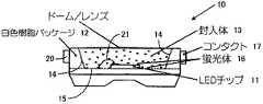
図1は、樹脂を加熱して粘度を下げるステップの前に、蛍光体16が封入体13の中に懸濁されていることを示す、本発明によるパッケージ化されているダイオードの断面図である。例示される実施形態は、表面実装横向きタイプ(side view surface mount)の応用形態を表す(「サイドルッカ」とも呼ばれる)。そのパッケージ化されているダイオードは、全体として10で示されており、パッケージ12上にLEDチップ11を含み、パッケージ12は典型的には、最大限に光を反射するために白色ポリマー樹脂から形成される。封入体13(たとえば、先に参照されたようにポリシロキサン)が、パッケージ12の側壁14及び15によって形成される凹部を満たす。蛍光体は黒い点16として示される。LEDチップ11のための適当な電気的コンタクト17及び20が潜在的にワイヤ21と共に設けられる。 FIG. 1 is a cross-sectional view of a packaged diode according to the present invention showing that the phosphor 16 is suspended in the encapsulant 13 prior to the step of heating the resin to reduce the viscosity. . The illustrated embodiment represents a side view surface mount application (also referred to as a “side looker”). The packaged diode is indicated generally at 10 and includes an LED chip 11 on a package 12, which is typically formed from a white polymer resin for maximum light reflection. Is done. Encapsulant 13 (eg, polysiloxane as previously referenced) fills the recess formed by sidewalls 14 and 15 of package 12. The phosphor is shown as black dots 16. Appropriate
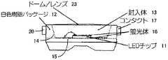
図2及び図3は、蛍光体16を沈降できるようにした後の本発明の2つの実施形態を示す。類似の構成要素は、図1の場合と同様の参照符号を有する。図2に示されるように、封入体13はもはや、蛍光体16の大部分を懸濁した状態で保有するのではなく、硬化して凹形メニスカス22を形成している。蛍光体16は、チップ11上、且つパッケージ12の底部15に沿って配置される(底部は典型的には、少なくとも1つの金属コンタクトを含む)。 2 and 3 show two embodiments of the present invention after allowing the phosphor 16 to settle. Similar components have the same reference numbers as in FIG. As shown in FIG. 2, the enclosure 13 no longer holds the majority of the phosphor 16 in a suspended state, but cures to form a concave meniscus 22. The phosphor 16 is disposed on the chip 11 and along the bottom 15 of the package 12 (the bottom typically includes at least one metal contact).
図1〜図3の向きは、制限するものではなく例示的であり、異なる壁部に対して、又は異なる位置に蛍光体を沈降させることが望ましい場合には、蛍光体がそのとおりに動くように、パッケージを向けることができることは理解されよう。たとえば、その目的が、メニスカスの上に全ての蛍光体を有することであるならば、その工程は、図1〜図3に対して、上下逆に向けたチップで実施することができるであろう。 The orientation of FIGS. 1-3 is exemplary rather than limiting, so that if it is desired to settle the phosphor against different walls or at different locations, the phosphor will move accordingly. It will be appreciated that the package can be directed to the other. For example, if the goal is to have all the phosphors on the meniscus, the process could be performed with the chip turned upside down with respect to FIGS. .
図1、図2及び図3では、LEDチップ11として、任意の適当な発光ダイオードを用いることができるが、本発明は、本発明の譲受人であるCree社(Durham, NC USA)から市販されるものを含む、青色発光ダイオードに関して特に好都合である。しかしながら、当業者は多種多様な発光ダイオードを十分に理解しており、それゆえ、Cree社製ダイオードは、本発明に従って用いることができるダイオードを限定するのではなく、例示として提供される。 1, 2 and 3, any suitable light emitting diode can be used as the LED chip 11, but the present invention is commercially available from Cree (Durham, NC USA), the assignee of the present invention. Particularly advantageous with respect to blue light emitting diodes, including However, those skilled in the art are well aware of a wide variety of light emitting diodes and, therefore, the Cree diodes are provided by way of illustration, not limitation of diodes that can be used in accordance with the present invention.
図3は、図2に類似の実施形態を示すが、メニスカス23が平坦な表面又はわずかにドーム形を形成している。平坦な又はわずかにドーム形(球形又は半球ではない)のメニスカスの利点は、2006年9月1日に出願された「Encapsulant Profile for Light Emitting Diodes」と題する、同じ譲受人に譲渡される特許出願第60/824,390号に記載されており、その内容は、参照により全体が本明細書に援用される。図3の個々の構成要素の残りのもの、及びそれらの構成要素の位置は、図2の場合と同じである。 FIG. 3 shows an embodiment similar to FIG. 2, but the meniscus 23 forms a flat surface or slightly domed. The benefit of a flat or slightly dome-shaped (not spherical or hemispherical) meniscus is the patent application assigned to the same assignee entitled “Encapsulant Profile for Light Emitting Diodes” filed on September 1, 2006. No. 60 / 824,390, the contents of which are hereby incorporated by reference in their entirety. The remaining individual components in FIG. 3 and the positions of those components are the same as in FIG.
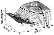
図4は、本発明の方法の態様を示す3次元プロットである。時間及び温度が直交する水平軸上にプロットされており、一方、粘度が(恣意的な対数単位で)垂直にプロットされる。こうして、結果として生成される3次元画像は、時間、温度及び粘度の多数の点における樹脂の反応を表す。したがって、時間及び温度の交点において開始するとき、1時間又は2時間の間に温度を約80℃又はそれ以上まで上昇させる結果として、樹脂が硬化する(すなわち、平坦域に入る)であろう。別法では、温度が比較的適度に保たれる場合には、非常に長い時間が経過しても、樹脂が硬化しないようにすることができる。 FIG. 4 is a three-dimensional plot showing aspects of the method of the present invention. Time and temperature are plotted on orthogonal horizontal axes, while viscosity is plotted vertically (in arbitrary logarithmic units). Thus, the resulting three-dimensional image represents the reaction of the resin at a number of points in time, temperature and viscosity. Thus, when starting at the intersection of time and temperature, the resin will cure (ie, enter a plateau) as a result of raising the temperature to about 80 ° C. or higher during one or two hours. Alternatively, if the temperature is kept relatively moderate, the resin can be prevented from curing after a very long time.
しかしながら、図4は、温度をさらに緩やかに上昇させる、すなわち約40℃から80℃まで上昇させる場合は、室温に比べて、樹脂の粘度が減少することを示す。したがって、図4は、実質的に室温と80℃との間で谷に類似の温度−粘度画像を示す。 However, FIG. 4 shows that when the temperature is increased more slowly, ie, from about 40 ° C. to 80 ° C., the viscosity of the resin decreases compared to room temperature. Accordingly, FIG. 4 shows a temperature-viscosity image similar to a valley substantially between room temperature and 80 ° C.
したがって、本発明の例示的な実施形態では、樹脂及び蛍光体は最初に、図4において数字1によって示される時間及び温度(約40℃)において混合される。ポットライフの一部が、数字1と2との間の矢印によって表される。数字2と3との間の破線は、蛍光体が沈降するほど十分に粘度が減少する温度(この実施形態では、約40℃と80℃との間)まで樹脂を加熱するステップを表す。数字3と4との間の線は、樹脂の粘度が低いままにしておいて、蛍光体が沈降できるようにする時間間隔を表す。当然、蛍光体が沈降できるようにする時間に対する仮定的な上限はなく、10分程度の短い時間間隔が、又は5時間程度の長い時間間隔が適していることがあるが、より典型的には、30分〜1時間である。 Thus, in an exemplary embodiment of the invention, the resin and phosphor are first mixed at the time and temperature (approximately 40 ° C.) indicated by the numeral 1 in FIG. A part of the pot life is represented by an arrow between the numbers 1 and 2. The dashed line between the numbers 2 and 3 represents the step of heating the resin to a temperature (between about 40 ° C. and 80 ° C. in this embodiment) at which the viscosity is reduced enough for the phosphor to settle. The line between the numbers 3 and 4 represents the time interval allowing the phosphor to settle while the viscosity of the resin remains low. Of course, there is no hypothetical upper limit for the time to allow the phosphors to settle, and a short time interval of about 10 minutes or a long time interval of about 5 hours may be suitable, but more typically 30 minutes to 1 hour.
数字4と5との間の線は、樹脂が比較的迅速に硬化することになる温度(たとえば、一般的には約100℃〜200℃であり、例示される実施形態では約140℃)まで温度を上昇させるステップを表しており、硬化そのものは、数字5と6との間の線によって表される。 The line between the numbers 4 and 5 is up to a temperature at which the resin will cure relatively quickly (eg, typically between about 100 ° C. and 200 ° C., and in the illustrated embodiment about 140 ° C.). It represents the step of increasing the temperature, the cure itself being represented by the line between the numbers 5 and 6.
樹脂を硬化させることが唯一の目的であるならば、できる限り真直ぐに位置1から位置6まで進むことによって、たとえば、約2時間で約120℃まで樹脂を加熱することによって、樹脂を硬化させることができることは理解されよう。しかしながら、本発明によれば、図4に示されるようにして、樹脂の特性を利用することによって、最終的なランプパッケージ内の蛍光体の位置を都合良く制御することができることがわかる。 If the sole purpose is to cure the resin, cure the resin by going from position 1 to position 6 as straight as possible, for example, by heating the resin to about 120 ° C. in about 2 hours. You will understand that you can. However, according to the present invention, as shown in FIG. 4, it can be seen that the position of the phosphor in the final lamp package can be conveniently controlled by utilizing the characteristics of the resin.
図面及び明細書では、本発明の好ましい一実施形態が記載されており、特定の用語が用いられてきたが、それらの用語は一般的で、説明するだけの意味で用いられており、限定するものではなく、本発明の範囲は特許請求の範囲において規定される。 In the drawings and specification, a preferred embodiment of the present invention has been described and specific terms have been used, but the terms are general and only meant to be described and limited Rather, the scope of the invention is defined in the claims.
10 ダイオード
11 LEDチップ
12 白色樹脂パッケージ
13 封入体
14 側壁
15 底部
16 蛍光体
17、20 コンタクト
21 ワイヤ
22、23 メニスカスDESCRIPTION OF
Claims (27)
Translated fromJapanese粘度を温度に応じて制御することができる硬化していないポリマー樹脂に複数の蛍光体粒子を混合し、該樹脂内に前記蛍光体粒子の実質的に均一な懸濁物を形成するステップ、
LEDチップに隣接する画定されている位置に前記硬化していない樹脂を配置するステップ、
前記樹脂が不適当に急速に硬化することになる温度よりも低い範囲で、前記樹脂の前記温度を上昇させていき、それに応じて該樹脂の粘度を減少させるステップ、
前記蛍光体粒子を、前記粘度が減少した樹脂内で、前記LEDチップに対する所望の位置に沈降させるステップ、及び
その後、前記樹脂の前記温度を、該樹脂が硬化し、固体になる温度まで上昇させるステップ
を含む、方法。A method of dispersing a phosphor in a desired state to form an LED lamp, the method comprising:
Mixing a plurality of phosphor particles with an uncured polymer resin whose viscosity can be controlled as a function of temperature to form a substantially uniform suspension of the phosphor particles in the resin;
Placing the uncured resin in a defined position adjacent to the LED chip;
Increasing the temperature of the resin in a range lower than the temperature at which the resin will improperly and rapidly cure, and reducing the viscosity of the resin accordingly.
Allowing the phosphor particles to settle to a desired position relative to the LED chip within the resin with reduced viscosity; and then raising the temperature of the resin to a temperature at which the resin cures and becomes solid. A method comprising steps.
電磁スペクトルの青色又はそれよりも高いエネルギー部分の光によって最小限にしか影響を受けない樹脂を組み込むことを含む、方法。The method of claim 1, wherein
Incorporating a resin that is minimally affected by light in the blue or higher energy portion of the electromagnetic spectrum.
ポリシロキサン樹脂を組み込むことを含む、方法。The method of claim 2, wherein
Incorporating a polysiloxane resin.
適度な温度において前記樹脂内に懸濁されたままになるが、前記樹脂の前記粘度が減少するときに、適度な時間内に沈降する特定の粒径を有する蛍光体を組み込むことを含む、方法。The method of claim 1, wherein
Incorporating a phosphor having a specific particle size that remains suspended in the resin at a moderate temperature but settles in a reasonable time when the viscosity of the resin decreases. .
前記蛍光体粒子を混合するステップは、前記硬化していないポリマー樹脂に、セリウム添加イットリウム−アルミニウム−ガーネットの粒子を混合することを含む、方法。The method of claim 1, wherein
The step of mixing the phosphor particles includes mixing cerium-doped yttrium-aluminum-garnet particles with the uncured polymer resin.
約6ミクロンの平均粒径を有する蛍光体粒子を混合することを含む、方法。The method of claim 5, wherein
Mixing phosphor particles having an average particle size of about 6 microns.
前記LEDチップに隣接する前記画定されている位置に前記樹脂を配置するステップの前に、約25℃〜約40℃の温度において、前記蛍光体粒子及び前記硬化していないポリマー樹脂を混合することを含む、方法。The method of claim 1, wherein
Mixing the phosphor particles and the uncured polymer resin at a temperature of about 25 ° C. to about 40 ° C. prior to placing the resin at the defined location adjacent to the LED chip. Including a method.
前記画定されている位置に前記硬化してない樹脂を配置するステップの後に、該樹脂の前記温度を約40℃〜80℃まで上昇させるステップを含む、方法。The method of claim 7, wherein
After placing the uncured resin in the defined position, raising the temperature of the resin to about 40 ° C to 80 ° C.
前記樹脂の前記温度を該樹脂が硬化することになる温度まで上昇させるステップは、該樹脂を約100℃〜200℃の温度まで加熱することを含む、方法。The method of claim 1, wherein
Raising the temperature of the resin to a temperature at which the resin will cure comprises heating the resin to a temperature of about 100 ° C to 200 ° C.
前記パッケージ化される発光ダイオードを光導波路と共に組み込む、ディスプレイ。The display according to claim 10, wherein
A display incorporating the light emitting diode to be packaged with an optical waveguide.
蛍光体及び樹脂を選択すると共に混合して懸濁物にし、該懸濁物を、適当なランプパッケージに分配できるように十分な時間間隔にわたって適度な温度において均質状態とするステップ、
前記蛍光体及び樹脂の均質な混合物をランプパッケージに分配するステップ、
前記温度を中間的なより高い温度まで上昇させて前記樹脂の粘度を減少させる場合に、前記蛍光体が所望の位置に沈降できるように、前記ランプパッケージを向けるステップ、
前記蛍光体が前記所望の位置に沈降するだけの十分な時間にわたって、前記中間的なより高い温度まで前記温度を上昇させ、前記樹脂の粘度を減少させるステップ、及び
前記蛍光体が前記所望の位置にある状態で、前記樹脂が適当な時間間隔内に硬化する温度まで前記温度を上昇させるステップ
を含む、LEDランプを形成する方法。A method of forming an LED lamp, comprising:
Selecting and mixing the phosphor and resin into a suspension, and homogenizing the suspension at a moderate temperature for a sufficient time interval so that it can be dispensed into a suitable lamp package;
Dispensing the homogeneous mixture of phosphor and resin into a lamp package;
Directing the lamp package so that the phosphor can settle to a desired location when the temperature is raised to an intermediate higher temperature to reduce the viscosity of the resin;
Increasing the temperature to the intermediate higher temperature and reducing the viscosity of the resin for a time sufficient for the phosphor to settle to the desired location; and A method of forming an LED lamp, comprising raising the temperature to a temperature at which the resin cures within a suitable time interval.
セリウム添加イットリウム−アルミニウム−ガーネット及びポリシロキサン樹脂の組み合わせを混合して前記均質な懸濁物にすることを含む、方法。The method of claim 13, wherein
Mixing a cerium-doped yttrium-aluminum-garnet and polysiloxane resin combination into the homogeneous suspension.
約6ミクロンの平均粒径を有する蛍光体を混合することを含む、方法。15. The method of claim 14, wherein
Mixing a phosphor having an average particle size of about 6 microns.
前記ランプパッケージを向けるステップは、前記蛍光体がLEDチップの上方及びその上に沈降するように前記ランプパッケージを向けることを含む、方法。The method of claim 13, wherein
Orienting the lamp package includes directing the lamp package such that the phosphor settles over and above the LED chip.
前記蛍光体及び前記樹脂を混合するステップは、実質的に室温において実行される、方法。The method of claim 13, wherein
The method wherein the step of mixing the phosphor and the resin is performed at substantially room temperature.
前記温度を前記中間的なより高い温度まで上昇させるステップは、該温度を約40℃〜80℃まで上昇させることを含む、方法。The method of claim 13, wherein
Raising the temperature to the intermediate higher temperature comprises raising the temperature to about 40 ° C to 80 ° C.
前記温度を前記樹脂が硬化する温度まで上昇させるステップは、該温度を約100℃〜200℃まで上昇させることを含む、方法。The method of claim 13, wherein
Increasing the temperature to a temperature at which the resin cures includes increasing the temperature to about 100 ° C to 200 ° C.
封入体を保持するためのくぼみ部を含むパッケージと、
前記パッケージの前記くぼみ部の底部上にあるLEDチップと、
前記LEDチップを覆い、前記くぼみ部の少なくとも一部を満たす封入体と、
前記封入体内にあり、主に前記LEDチップ上に、且つ前記パッケージの前記底部に沿って分布する蛍光体と
を含む、LEDランプ。An LED lamp,
A package including an indentation for holding the inclusion body;
An LED chip on the bottom of the indentation of the package;
An enclosure that covers the LED chip and fills at least a portion of the indented portion;
An LED lamp that is in the enclosure and includes phosphors that are distributed mainly on the LED chip and along the bottom of the package.
前記パッケージは白色ポリマー樹脂である、LEDランプ。The LED lamp according to claim 20,
The LED lamp, wherein the package is a white polymer resin.
前記LEDチップは、第III族窒化物材料系から選択される発光部分を含み、可視スペクトルの青色部分を放射する、LEDランプ。21. The LED lamp of claim 20, wherein the LED chip includes a light emitting portion selected from a Group III nitride material system and emits a blue portion of the visible spectrum.
前記蛍光体はセリウム添加YAGを含む、LEDランプ。The LED lamp according to claim 20,
The phosphor is an LED lamp including cerium-added YAG.
前記蛍光体は、約6ミクロンの平均粒径を有する粒子から形成される、LEDランプ。The LED lamp according to claim 23,
The LED lamp is formed of particles having an average particle size of about 6 microns.
前記封入体はポリシロキサン樹脂を含む、LEDランプ。The LED lamp according to claim 20,
The enclosure includes an LED lamp including a polysiloxane resin.
前記封入体は凹形メニスカスを画定する、LEDランプ。The LED lamp according to claim 20,
An LED lamp, wherein the enclosure defines a concave meniscus.
前記封入体は凸形メニスカスを画定する、LEDランプ。The LED lamp according to claim 20,
An LED lamp wherein the enclosure defines a convex meniscus.
Applications Claiming Priority (4)
| Application Number | Priority Date | Filing Date | Title |
|---|---|---|---|
| US82438506P | 2006-09-01 | 2006-09-01 | |
| US60/824,385 | 2006-09-01 | ||
| US11/839,562US8425271B2 (en) | 2006-09-01 | 2007-08-16 | Phosphor position in light emitting diodes |
| US11/839,562 | 2007-08-16 |
Related Child Applications (1)
| Application Number | Title | Priority Date | Filing Date |
|---|---|---|---|
| JP2011224055ADivisionJP2012009905A (en) | 2006-09-01 | 2011-10-11 | Position of phosphor in light emitting diode |
Publications (2)
| Publication Number | Publication Date |
|---|---|
| JP2008103688Atrue JP2008103688A (en) | 2008-05-01 |
| JP4929100B2 JP4929100B2 (en) | 2012-05-09 |
Family
ID=39047133
Family Applications (2)
| Application Number | Title | Priority Date | Filing Date |
|---|---|---|---|
| JP2007216808AActiveJP4929100B2 (en) | 2006-09-01 | 2007-08-23 | Location of phosphor in light-emitting diode |
| JP2011224055ARevokedJP2012009905A (en) | 2006-09-01 | 2011-10-11 | Position of phosphor in light emitting diode |
Family Applications After (1)
| Application Number | Title | Priority Date | Filing Date |
|---|---|---|---|
| JP2011224055ARevokedJP2012009905A (en) | 2006-09-01 | 2011-10-11 | Position of phosphor in light emitting diode |
Country Status (4)
| Country | Link |
|---|---|
| US (1) | US8425271B2 (en) |
| JP (2) | JP4929100B2 (en) |
| CN (2) | CN101232065B (en) |
| DE (1) | DE102007040841B4 (en) |
Cited By (18)
| Publication number | Priority date | Publication date | Assignee | Title |
|---|---|---|---|---|
| US8373182B2 (en) | 2010-09-09 | 2013-02-12 | Stanley Electric Co., Ltd. | Semiconductor light-emitting device and manufacturing method |
| US8455907B2 (en) | 2010-06-16 | 2013-06-04 | Stanley Electric Co., Ltd. | Semiconductor light emitting device having an optical plate including a meniscus control structure and method of manufacturing |
| JP2013520824A (en)* | 2010-02-26 | 2013-06-06 | オスラム オプト セミコンダクターズ ゲゼルシャフト ミット ベシュレンクテル ハフツング | Radiation emission apparatus provided with semiconductor chip and conversion element, and manufacturing method thereof |
| US8461610B2 (en) | 2010-06-16 | 2013-06-11 | Stanley Electric Co., Ltd. | Semiconductor light emitting device having a reflective material with a side slant surface and method of manufacturing |
| JP2013197309A (en)* | 2012-03-19 | 2013-09-30 | Toshiba Corp | Light-emitting device |
| WO2013146607A1 (en)* | 2012-03-30 | 2013-10-03 | 富士フイルム株式会社 | Sealing agent for semiconductor light emitting elements, cured film using same, and semiconductor light emitting device |
| US8581287B2 (en) | 2011-01-24 | 2013-11-12 | Stanley Electric Co., Ltd. | Semiconductor light emitting device having a reflective material, wavelength converting layer and optical plate with rough and plane surface regions, and method of manufacturing |
| US8921877B2 (en) | 2010-08-02 | 2014-12-30 | Stanley Electric Co., Ltd. | Semiconductor light-emitting device for producing wavelength-converted light and method for manufacturing the same |
| JP2016058614A (en)* | 2014-09-11 | 2016-04-21 | パナソニックIpマネジメント株式会社 | Light emitting device and lighting device |
| US9368690B2 (en) | 2013-01-24 | 2016-06-14 | Stanley Electric Co., Ltd. | Semiconductor light-emitting device |
| US9472730B2 (en) | 2014-03-28 | 2016-10-18 | Toyoda Gosei Co., Ltd. | Light emitting device |
| US9484507B2 (en) | 2013-06-28 | 2016-11-01 | Nichia Corporation | Light emitting device |
| JP2017022360A (en)* | 2015-07-13 | 2017-01-26 | 豊田合成株式会社 | Method for manufacturing light emitting device |
| US9728685B2 (en) | 2013-02-28 | 2017-08-08 | Nichia Corporation | Light emitting device and lighting device including same |
| US9954148B2 (en) | 2014-10-24 | 2018-04-24 | Citizen Electronics Co., Ltd. | Light-emitting apparatus with optical element and method of manufacturing the same |
| JP2019016820A (en)* | 2010-12-28 | 2019-01-31 | 日亜化学工業株式会社 | Light emitting device |
| US10461225B2 (en) | 2015-03-09 | 2019-10-29 | Toyoda Gosei Co., Ltd. | Method of manufacturing light-emitting device including sealing materials with phosphor particles |
| US10644192B2 (en) | 2015-07-13 | 2020-05-05 | Toyoda Gosei Co., Ltd. | Method of manufacturing light-emitting device |
Families Citing this family (63)
| Publication number | Priority date | Publication date | Assignee | Title |
|---|---|---|---|---|
| US7910938B2 (en)* | 2006-09-01 | 2011-03-22 | Cree, Inc. | Encapsulant profile for light emitting diodes |
| US7687823B2 (en)* | 2006-12-26 | 2010-03-30 | Nichia Corporation | Light-emitting apparatus and method of producing the same |
| US7955875B2 (en)* | 2008-09-26 | 2011-06-07 | Cree, Inc. | Forming light emitting devices including custom wavelength conversion structures |
| JP5477374B2 (en)* | 2009-03-27 | 2014-04-23 | コニカミノルタ株式会社 | Phosphor member, method for manufacturing phosphor member, and lighting device |
| US8547009B2 (en)* | 2009-07-10 | 2013-10-01 | Cree, Inc. | Lighting structures including diffuser particles comprising phosphor host materials |
| KR101253586B1 (en)* | 2010-08-25 | 2013-04-11 | 삼성전자주식회사 | Phosphor film, method of manufacturing the same, method of coating phosphor layer on an LED chip, method of manufacturing LED package and LED package manufactured thereof |
| US9515229B2 (en)* | 2010-09-21 | 2016-12-06 | Cree, Inc. | Semiconductor light emitting devices with optical coatings and methods of making same |
| USD721339S1 (en) | 2010-12-03 | 2015-01-20 | Cree, Inc. | Light emitter device |
| USD676000S1 (en) | 2010-11-22 | 2013-02-12 | Cree, Inc. | Light emitting device package |
| USD712850S1 (en) | 2010-11-18 | 2014-09-09 | Cree, Inc. | Light emitter device |
| US8564000B2 (en) | 2010-11-22 | 2013-10-22 | Cree, Inc. | Light emitting devices for light emitting diodes (LEDs) |
| USD707192S1 (en) | 2010-11-18 | 2014-06-17 | Cree, Inc. | Light emitting device |
| US10267506B2 (en) | 2010-11-22 | 2019-04-23 | Cree, Inc. | Solid state lighting apparatuses with non-uniformly spaced emitters for improved heat distribution, system having the same, and methods having the same |
| US9000470B2 (en) | 2010-11-22 | 2015-04-07 | Cree, Inc. | Light emitter devices |
| US9490235B2 (en) | 2010-11-22 | 2016-11-08 | Cree, Inc. | Light emitting devices, systems, and methods |
| USD650760S1 (en) | 2010-11-22 | 2011-12-20 | Cree, Inc. | Light emitting device package |
| US8575639B2 (en) | 2011-02-16 | 2013-11-05 | Cree, Inc. | Light emitting devices for light emitting diodes (LEDs) |
| US9300062B2 (en) | 2010-11-22 | 2016-03-29 | Cree, Inc. | Attachment devices and methods for light emitting devices |
| US8624271B2 (en) | 2010-11-22 | 2014-01-07 | Cree, Inc. | Light emitting devices |
| USD706231S1 (en) | 2010-12-03 | 2014-06-03 | Cree, Inc. | Light emitting device |
| US8809880B2 (en) | 2011-02-16 | 2014-08-19 | Cree, Inc. | Light emitting diode (LED) chips and devices for providing failure mitigation in LED arrays |
| US8455908B2 (en) | 2011-02-16 | 2013-06-04 | Cree, Inc. | Light emitting devices |
| USD702653S1 (en) | 2011-10-26 | 2014-04-15 | Cree, Inc. | Light emitting device component |
| CN102646761B (en)* | 2011-02-21 | 2014-10-15 | 展晶科技(深圳)有限公司 | LED packaging process |
| US9365766B2 (en)* | 2011-10-13 | 2016-06-14 | Intematix Corporation | Wavelength conversion component having photo-luminescence material embedded into a hermetic material for remote wavelength conversion |
| USD705181S1 (en) | 2011-10-26 | 2014-05-20 | Cree, Inc. | Light emitting device component |
| KR20140097284A (en) | 2011-11-07 | 2014-08-06 | 크리,인코포레이티드 | High voltage array light emitting diode(led) devices, fixtures and methods |
| US9806246B2 (en) | 2012-02-07 | 2017-10-31 | Cree, Inc. | Ceramic-based light emitting diode (LED) devices, components, and methods |
| US9735198B2 (en) | 2012-03-30 | 2017-08-15 | Cree, Inc. | Substrate based light emitter devices, components, and related methods |
| US10134961B2 (en) | 2012-03-30 | 2018-11-20 | Cree, Inc. | Submount based surface mount device (SMD) light emitter components and methods |
| US9345091B2 (en) | 2013-02-08 | 2016-05-17 | Cree, Inc. | Light emitting device (LED) light fixture control systems and related methods |
| US8933478B2 (en) | 2013-02-19 | 2015-01-13 | Cooledge Lighting Inc. | Engineered-phosphor LED packages and related methods |
| US8754435B1 (en) | 2013-02-19 | 2014-06-17 | Cooledge Lighting Inc. | Engineered-phosphor LED package and related methods |
| US10295124B2 (en)* | 2013-02-27 | 2019-05-21 | Cree, Inc. | Light emitter packages and methods |
| JP6323048B2 (en)* | 2013-03-15 | 2018-05-16 | 株式会社リコー | Distribution system, distribution method, and program |
| JP2014192502A (en) | 2013-03-28 | 2014-10-06 | Toyoda Gosei Co Ltd | Method of manufacturing light-emitting device |
| USD739565S1 (en) | 2013-06-27 | 2015-09-22 | Cree, Inc. | Light emitter unit |
| USD740453S1 (en) | 2013-06-27 | 2015-10-06 | Cree, Inc. | Light emitter unit |
| WO2016084437A1 (en)* | 2014-11-28 | 2016-06-02 | シャープ株式会社 | Light emitting device and lighting device |
| US9826581B2 (en) | 2014-12-05 | 2017-11-21 | Cree, Inc. | Voltage configurable solid state lighting apparatuses, systems, and related methods |
| US10431568B2 (en) | 2014-12-18 | 2019-10-01 | Cree, Inc. | Light emitting diodes, components and related methods |
| KR102346798B1 (en) | 2015-02-13 | 2022-01-05 | 삼성전자주식회사 | Semiconductor light emitting device |
| DE102016112275B4 (en)* | 2016-07-05 | 2022-10-06 | OSRAM Opto Semiconductors Gesellschaft mit beschränkter Haftung | METHOD FOR MANUFACTURING OPTOELECTRONIC LUMINATING DEVICE AND OPTOELECTRONIC LUMINATING DEVICE |
| EP3491679B1 (en) | 2016-07-26 | 2023-02-22 | CreeLED, Inc. | Light emitting diodes, components and related methods |
| WO2018052902A1 (en) | 2016-09-13 | 2018-03-22 | Cree, Inc. | Light emitting diodes, components and related methods |
| JP6493348B2 (en)* | 2016-09-30 | 2019-04-03 | 日亜化学工業株式会社 | Light emitting device |
| USD823492S1 (en) | 2016-10-04 | 2018-07-17 | Cree, Inc. | Light emitting device |
| US10164159B2 (en) | 2016-12-20 | 2018-12-25 | Samsung Electronics Co., Ltd. | Light-emitting diode package and method of manufacturing the same |
| US10439114B2 (en) | 2017-03-08 | 2019-10-08 | Cree, Inc. | Substrates for light emitting diodes and related methods |
| US11101248B2 (en) | 2017-08-18 | 2021-08-24 | Creeled, Inc. | Light emitting diodes, components and related methods |
| US11107857B2 (en) | 2017-08-18 | 2021-08-31 | Creeled, Inc. | Light emitting diodes, components and related methods |
| US10361349B2 (en) | 2017-09-01 | 2019-07-23 | Cree, Inc. | Light emitting diodes, components and related methods |
| US11121298B2 (en) | 2018-05-25 | 2021-09-14 | Creeled, Inc. | Light-emitting diode packages with individually controllable light-emitting diode chips |
| WO2020003789A1 (en) | 2018-06-29 | 2020-01-02 | 日亜化学工業株式会社 | Method for producing light emitting device, and light emitting device |
| US11233183B2 (en) | 2018-08-31 | 2022-01-25 | Creeled, Inc. | Light-emitting diodes, light-emitting diode arrays and related devices |
| US11335833B2 (en) | 2018-08-31 | 2022-05-17 | Creeled, Inc. | Light-emitting diodes, light-emitting diode arrays and related devices |
| US11101411B2 (en) | 2019-06-26 | 2021-08-24 | Creeled, Inc. | Solid-state light emitting devices including light emitting diodes in package structures |
| US12278219B2 (en) | 2020-12-21 | 2025-04-15 | Creeled, Inc. | LED chips and devices with textured light-extracting portions, and fabrication methods |
| KR20230000009A (en)* | 2021-06-23 | 2023-01-02 | 삼성전자주식회사 | Semiconductor light emitting device and semiconductor light emitting device array |
| US11870009B2 (en) | 2021-08-06 | 2024-01-09 | Creeled, Inc. | Edge structures for light shaping in light-emitting diode chips |
| CN114937719B (en)* | 2022-04-28 | 2024-11-12 | 福建晶旭半导体科技有限公司 | Phosphor glue dispensing method and light-emitting device thereof |
| CN118610203B (en)* | 2024-06-14 | 2025-03-28 | 深圳市正通仁禾科技有限公司 | Display panel and electronic equipment |
| CN118472155A (en)* | 2024-07-12 | 2024-08-09 | 江西省兆驰光电有限公司 | LED light source, packaging method thereof and lamp |
Citations (10)
| Publication number | Priority date | Publication date | Assignee | Title |
|---|---|---|---|---|
| JP2000101147A (en)* | 1998-09-22 | 2000-04-07 | Nichia Chem Ind Ltd | Semiconductor device and manufacturing method thereof |
| JP2002076445A (en)* | 2000-09-01 | 2002-03-15 | Sanken Electric Co Ltd | Semiconductor light emitting device |
| JP2003046141A (en)* | 2001-07-31 | 2003-02-14 | Nichia Chem Ind Ltd | Light emitting device and manufacturing method thereof |
| JP2003224307A (en)* | 2003-02-06 | 2003-08-08 | Nichia Chem Ind Ltd | Light emitting diode and method of forming the same |
| JP2003234511A (en)* | 2002-02-06 | 2003-08-22 | Toshiba Corp | Semiconductor light emitting device and method of manufacturing the same |
| JP2004134699A (en)* | 2002-10-15 | 2004-04-30 | Toyoda Gosei Co Ltd | Light emitting device |
| JP2004186488A (en)* | 2002-12-04 | 2004-07-02 | Nichia Chem Ind Ltd | Light emitting device, method of manufacturing light emitting device, and method of adjusting chromaticity of light emitting device |
| JP2005167079A (en)* | 2003-12-04 | 2005-06-23 | Toyoda Gosei Co Ltd | Light emitting device |
| JP2006114637A (en)* | 2004-10-13 | 2006-04-27 | Toshiba Corp | Semiconductor light emitting device |
| JP2006165416A (en)* | 2004-12-10 | 2006-06-22 | Stanley Electric Co Ltd | White display and manufacturing method thereof |
Family Cites Families (40)
| Publication number | Priority date | Publication date | Assignee | Title |
|---|---|---|---|---|
| DE19638667C2 (en)* | 1996-09-20 | 2001-05-17 | Osram Opto Semiconductors Gmbh | Mixed-color light-emitting semiconductor component with luminescence conversion element |
| TW383508B (en) | 1996-07-29 | 2000-03-01 | Nichia Kagaku Kogyo Kk | Light emitting device and display |
| US6274890B1 (en)* | 1997-01-15 | 2001-08-14 | Kabushiki Kaisha Toshiba | Semiconductor light emitting device and its manufacturing method |
| JP3492178B2 (en)* | 1997-01-15 | 2004-02-03 | 株式会社東芝 | Semiconductor light emitting device and method of manufacturing the same |
| US6257737B1 (en)* | 1999-05-20 | 2001-07-10 | Philips Electronics Na | Low-profile luminaire having a reflector for mixing light from a multi-color linear array of LEDs |
| US20020063520A1 (en)* | 2000-11-29 | 2002-05-30 | Huei-Che Yu | Pre-formed fluorescent plate - LED device |
| AT410266B (en)* | 2000-12-28 | 2003-03-25 | Tridonic Optoelectronics Gmbh | LIGHT SOURCE WITH A LIGHT-EMITTING ELEMENT |
| MY145695A (en)* | 2001-01-24 | 2012-03-30 | Nichia Corp | Light emitting diode, optical semiconductor device, epoxy resin composition suited for optical semiconductor device, and method for manufacturing the same |
| US6664560B2 (en) | 2001-06-15 | 2003-12-16 | Cree, Inc. | Ultraviolet light emitting diode |
| JP2006080565A (en)* | 2001-09-03 | 2006-03-23 | Matsushita Electric Ind Co Ltd | Manufacturing method of semiconductor light emitting device |
| JP3948650B2 (en)* | 2001-10-09 | 2007-07-25 | アバゴ・テクノロジーズ・イーシービーユー・アイピー(シンガポール)プライベート・リミテッド | Light emitting diode and manufacturing method thereof |
| EP1453107A4 (en)* | 2001-11-16 | 2008-12-03 | Toyoda Gosei Kk | LIGHT EMITTING DIODE, DIODE LIGHTING AND LIGHTING DEVICE |
| TW200414572A (en)* | 2002-11-07 | 2004-08-01 | Matsushita Electric Industrial Co Ltd | LED lamp |
| US7042020B2 (en) | 2003-02-14 | 2006-05-09 | Cree, Inc. | Light emitting device incorporating a luminescent material |
| JP4254266B2 (en)* | 2003-02-20 | 2009-04-15 | 豊田合成株式会社 | LIGHT EMITTING DEVICE AND LIGHT EMITTING DEVICE MANUFACTURING METHOD |
| JP4131178B2 (en)* | 2003-02-28 | 2008-08-13 | 豊田合成株式会社 | Light emitting device |
| KR100537560B1 (en)* | 2003-11-25 | 2005-12-19 | 주식회사 메디아나전자 | Manufacturing method for white Light Emitting Diode device including two step cure process |
| CN1317775C (en)* | 2003-12-10 | 2007-05-23 | 玄基光电半导体股份有限公司 | Light-emitting diode packaging structure and packaging method thereof |
| JP2005197369A (en) | 2004-01-05 | 2005-07-21 | Toshiba Corp | Optical semiconductor device |
| JP4357311B2 (en)* | 2004-02-04 | 2009-11-04 | シチズン電子株式会社 | Light emitting diode chip |
| US7246923B2 (en)* | 2004-02-11 | 2007-07-24 | 3M Innovative Properties Company | Reshaping light source modules and illumination systems using the same |
| JP4516337B2 (en) | 2004-03-25 | 2010-08-04 | シチズン電子株式会社 | Semiconductor light emitting device |
| US7517728B2 (en)* | 2004-03-31 | 2009-04-14 | Cree, Inc. | Semiconductor light emitting devices including a luminescent conversion element |
| US7419912B2 (en) | 2004-04-01 | 2008-09-02 | Cree, Inc. | Laser patterning of light emitting devices |
| TWI241034B (en)* | 2004-05-20 | 2005-10-01 | Lighthouse Technology Co Ltd | Light emitting diode package |
| KR20060000313A (en)* | 2004-06-28 | 2006-01-06 | 루미마이크로 주식회사 | Method for producing a color conversion light-emitting device comprising a large particle fluorescent powder and a resin composition used therein |
| JP4747726B2 (en) | 2004-09-09 | 2011-08-17 | 豊田合成株式会社 | Light emitting device |
| US7737459B2 (en) | 2004-09-22 | 2010-06-15 | Cree, Inc. | High output group III nitride light emitting diodes |
| US8174037B2 (en) | 2004-09-22 | 2012-05-08 | Cree, Inc. | High efficiency group III nitride LED with lenticular surface |
| US8513686B2 (en) | 2004-09-22 | 2013-08-20 | Cree, Inc. | High output small area group III nitride LEDs |
| US7259402B2 (en) | 2004-09-22 | 2007-08-21 | Cree, Inc. | High efficiency group III nitride-silicon carbide light emitting diode |
| JP4756841B2 (en)* | 2004-09-29 | 2011-08-24 | スタンレー電気株式会社 | Manufacturing method of semiconductor light emitting device |
| JP4802533B2 (en)* | 2004-11-12 | 2011-10-26 | 日亜化学工業株式会社 | Semiconductor device |
| US8288942B2 (en) | 2004-12-28 | 2012-10-16 | Cree, Inc. | High efficacy white LED |
| TWI419375B (en)* | 2005-02-18 | 2013-12-11 | Nichia Corp | Light-emitting device with lens for controlling light distribution characteristics |
| US7405433B2 (en)* | 2005-02-22 | 2008-07-29 | Avago Technologies Ecbu Ip Pte Ltd | Semiconductor light emitting device |
| JP4876426B2 (en)* | 2005-04-08 | 2012-02-15 | 日亜化学工業株式会社 | Light emitting device with excellent heat resistance and light resistance |
| EP1710847B1 (en)* | 2005-04-08 | 2014-09-17 | Nichia Corporation | Light emitting device with silicone resin layer formed by screen printing |
| WO2007050483A2 (en)* | 2005-10-24 | 2007-05-03 | 3M Innovative Properties Company | Method of making light emitting device having a molded encapsulant |
| US20070269586A1 (en)* | 2006-05-17 | 2007-11-22 | 3M Innovative Properties Company | Method of making light emitting device with silicon-containing composition |
- 2007
- 2007-08-16USUS11/839,562patent/US8425271B2/enactiveActive
- 2007-08-23JPJP2007216808Apatent/JP4929100B2/enactiveActive
- 2007-08-29DEDE102007040841Apatent/DE102007040841B4/enactiveActive
- 2007-08-31CNCN2007101483269Apatent/CN101232065B/enactiveActive
- 2007-08-31CNCN201210175686.9Apatent/CN102683560B/enactiveActive
- 2011
- 2011-10-11JPJP2011224055Apatent/JP2012009905A/ennot_activeRevoked
Patent Citations (10)
| Publication number | Priority date | Publication date | Assignee | Title |
|---|---|---|---|---|
| JP2000101147A (en)* | 1998-09-22 | 2000-04-07 | Nichia Chem Ind Ltd | Semiconductor device and manufacturing method thereof |
| JP2002076445A (en)* | 2000-09-01 | 2002-03-15 | Sanken Electric Co Ltd | Semiconductor light emitting device |
| JP2003046141A (en)* | 2001-07-31 | 2003-02-14 | Nichia Chem Ind Ltd | Light emitting device and manufacturing method thereof |
| JP2003234511A (en)* | 2002-02-06 | 2003-08-22 | Toshiba Corp | Semiconductor light emitting device and method of manufacturing the same |
| JP2004134699A (en)* | 2002-10-15 | 2004-04-30 | Toyoda Gosei Co Ltd | Light emitting device |
| JP2004186488A (en)* | 2002-12-04 | 2004-07-02 | Nichia Chem Ind Ltd | Light emitting device, method of manufacturing light emitting device, and method of adjusting chromaticity of light emitting device |
| JP2003224307A (en)* | 2003-02-06 | 2003-08-08 | Nichia Chem Ind Ltd | Light emitting diode and method of forming the same |
| JP2005167079A (en)* | 2003-12-04 | 2005-06-23 | Toyoda Gosei Co Ltd | Light emitting device |
| JP2006114637A (en)* | 2004-10-13 | 2006-04-27 | Toshiba Corp | Semiconductor light emitting device |
| JP2006165416A (en)* | 2004-12-10 | 2006-06-22 | Stanley Electric Co Ltd | White display and manufacturing method thereof |
Cited By (23)
| Publication number | Priority date | Publication date | Assignee | Title |
|---|---|---|---|---|
| US8890140B2 (en) | 2010-02-26 | 2014-11-18 | Osram Opto Semiconductor Gmbh | Radiation-emitting component with a semiconductor chip and a conversion element and method for the production thereof |
| JP2013520824A (en)* | 2010-02-26 | 2013-06-06 | オスラム オプト セミコンダクターズ ゲゼルシャフト ミット ベシュレンクテル ハフツング | Radiation emission apparatus provided with semiconductor chip and conversion element, and manufacturing method thereof |
| KR101825044B1 (en)* | 2010-02-26 | 2018-02-02 | 오스람 옵토 세미컨덕터스 게엠베하 | Radiation-emitting component comprising a semiconductor chip and a conversion element and method for producing it |
| US8455907B2 (en) | 2010-06-16 | 2013-06-04 | Stanley Electric Co., Ltd. | Semiconductor light emitting device having an optical plate including a meniscus control structure and method of manufacturing |
| US8461610B2 (en) | 2010-06-16 | 2013-06-11 | Stanley Electric Co., Ltd. | Semiconductor light emitting device having a reflective material with a side slant surface and method of manufacturing |
| US8921877B2 (en) | 2010-08-02 | 2014-12-30 | Stanley Electric Co., Ltd. | Semiconductor light-emitting device for producing wavelength-converted light and method for manufacturing the same |
| US8373182B2 (en) | 2010-09-09 | 2013-02-12 | Stanley Electric Co., Ltd. | Semiconductor light-emitting device and manufacturing method |
| JP2019016820A (en)* | 2010-12-28 | 2019-01-31 | 日亜化学工業株式会社 | Light emitting device |
| US8581287B2 (en) | 2011-01-24 | 2013-11-12 | Stanley Electric Co., Ltd. | Semiconductor light emitting device having a reflective material, wavelength converting layer and optical plate with rough and plane surface regions, and method of manufacturing |
| JP2013197309A (en)* | 2012-03-19 | 2013-09-30 | Toshiba Corp | Light-emitting device |
| JP2013229538A (en)* | 2012-03-30 | 2013-11-07 | Fujifilm Corp | Sealant for semiconductor light-emitting element, cured film using the same, and semiconductor light-emitting device |
| WO2013146607A1 (en)* | 2012-03-30 | 2013-10-03 | 富士フイルム株式会社 | Sealing agent for semiconductor light emitting elements, cured film using same, and semiconductor light emitting device |
| US9368690B2 (en) | 2013-01-24 | 2016-06-14 | Stanley Electric Co., Ltd. | Semiconductor light-emitting device |
| US9793455B2 (en) | 2013-01-24 | 2017-10-17 | Stanley Electric Co., Ltd. | Semiconductor light-emitting device |
| US9728685B2 (en) | 2013-02-28 | 2017-08-08 | Nichia Corporation | Light emitting device and lighting device including same |
| US9608180B2 (en) | 2013-06-28 | 2017-03-28 | Nichia Corporation | Light emitting device |
| US9484507B2 (en) | 2013-06-28 | 2016-11-01 | Nichia Corporation | Light emitting device |
| US9472730B2 (en) | 2014-03-28 | 2016-10-18 | Toyoda Gosei Co., Ltd. | Light emitting device |
| JP2016058614A (en)* | 2014-09-11 | 2016-04-21 | パナソニックIpマネジメント株式会社 | Light emitting device and lighting device |
| US9954148B2 (en) | 2014-10-24 | 2018-04-24 | Citizen Electronics Co., Ltd. | Light-emitting apparatus with optical element and method of manufacturing the same |
| US10461225B2 (en) | 2015-03-09 | 2019-10-29 | Toyoda Gosei Co., Ltd. | Method of manufacturing light-emitting device including sealing materials with phosphor particles |
| JP2017022360A (en)* | 2015-07-13 | 2017-01-26 | 豊田合成株式会社 | Method for manufacturing light emitting device |
| US10644192B2 (en) | 2015-07-13 | 2020-05-05 | Toyoda Gosei Co., Ltd. | Method of manufacturing light-emitting device |
Also Published As
| Publication number | Publication date |
|---|---|
| CN102683560A (en) | 2012-09-19 |
| CN102683560B (en) | 2016-01-20 |
| DE102007040841B4 (en) | 2012-12-06 |
| JP2012009905A (en) | 2012-01-12 |
| CN101232065B (en) | 2012-07-04 |
| US20080054279A1 (en) | 2008-03-06 |
| US8425271B2 (en) | 2013-04-23 |
| JP4929100B2 (en) | 2012-05-09 |
| DE102007040841A1 (en) | 2008-03-13 |
| CN101232065A (en) | 2008-07-30 |
Similar Documents
| Publication | Publication Date | Title |
|---|---|---|
| JP4929100B2 (en) | Location of phosphor in light-emitting diode | |
| CN103180977B (en) | There is device and its manufacture method of the emitted radiation of the transition material with thermal conductive contact portion | |
| TWI298208B (en) | Light emitting device with a thermal insulating and refractive index matching material | |
| US8167674B2 (en) | Phosphor distribution in LED lamps using centrifugal force | |
| CN102800786B (en) | Light-emitting diode and display element | |
| TWI393841B (en) | Wide illuminating lens for backlighting diode | |
| US9243777B2 (en) | Rare earth optical elements for LED lamp | |
| US20080121911A1 (en) | Optical preforms for solid state light emitting dice, and methods and systems for fabricating and assembling same | |
| US20140151734A1 (en) | Light-emitting device and method for manufacturing same | |
| US20090039762A1 (en) | White led device comprising dual-mold and manufacturing method for the same | |
| US9318670B2 (en) | Materials for photoluminescence wavelength converted solid-state light emitting devices and arrangements | |
| JP2020184641A (en) | Manufacturing method of optoelectronic parts and optoelectronic parts | |
| WO2007135707A1 (en) | Resin molded body and surface-mounted light emitting device, and manufacturing method thereof | |
| JP2012256651A (en) | Resin package for semiconductor light-emitting device and manufacturing method therefor and semiconductor light-emitting device having resin package | |
| JP5868404B2 (en) | Phosphor suspended in silicone, molded / formed and used in a remote phosphor configuration | |
| WO2013138401A1 (en) | Metal-containing encapsulant compositions and methods | |
| JP5176273B2 (en) | Light emitting device and manufacturing method thereof | |
| KR100888487B1 (en) | Multichip LED Package with Diffusion Plate and Manufacturing Method Thereof | |
| Lin et al. | LED and optical device packaging and materials | |
| WO2013138402A1 (en) | Encapsulant compositions and methods for lighting devices | |
| JP2011222852A (en) | Optical semiconductor device | |
| US9041285B2 (en) | Phosphor distribution in LED lamps using centrifugal force | |
| KR20200099989A (en) | Resin composition for wafer level optical semiconductor device, and wafer level optical semicomductor device using said composition | |
| Chen | Cost-Effective White LED Lighting Backlighting Sources by Optimization of Packaging Materials and Processes | |
| JP2016225374A (en) | LED light emitting device |
Legal Events
| Date | Code | Title | Description |
|---|---|---|---|
| A131 | Notification of reasons for refusal | Free format text:JAPANESE INTERMEDIATE CODE: A131 Effective date:20100906 | |
| A601 | Written request for extension of time | Free format text:JAPANESE INTERMEDIATE CODE: A601 Effective date:20101206 | |
| RD03 | Notification of appointment of power of attorney | Free format text:JAPANESE INTERMEDIATE CODE: A7423 Effective date:20101206 | |
| A521 | Request for written amendment filed | Free format text:JAPANESE INTERMEDIATE CODE: A523 Effective date:20101220 | |
| A602 | Written permission of extension of time | Free format text:JAPANESE INTERMEDIATE CODE: A602 Effective date:20101224 | |
| RD04 | Notification of resignation of power of attorney | Free format text:JAPANESE INTERMEDIATE CODE: A7424 Effective date:20101228 | |
| A521 | Request for written amendment filed | Free format text:JAPANESE INTERMEDIATE CODE: A523 Effective date:20110307 | |
| A02 | Decision of refusal | Free format text:JAPANESE INTERMEDIATE CODE: A02 Effective date:20110609 | |
| A521 | Request for written amendment filed | Free format text:JAPANESE INTERMEDIATE CODE: A523 Effective date:20111011 | |
| A521 | Request for written amendment filed | Free format text:JAPANESE INTERMEDIATE CODE: A523 Effective date:20111121 | |
| A911 | Transfer to examiner for re-examination before appeal (zenchi) | Free format text:JAPANESE INTERMEDIATE CODE: A911 Effective date:20111128 | |
| TRDD | Decision of grant or rejection written | ||
| A01 | Written decision to grant a patent or to grant a registration (utility model) | Free format text:JAPANESE INTERMEDIATE CODE: A01 Effective date:20120112 | |
| A01 | Written decision to grant a patent or to grant a registration (utility model) | Free format text:JAPANESE INTERMEDIATE CODE: A01 | |
| A61 | First payment of annual fees (during grant procedure) | Free format text:JAPANESE INTERMEDIATE CODE: A61 Effective date:20120213 | |
| FPAY | Renewal fee payment (event date is renewal date of database) | Free format text:PAYMENT UNTIL: 20150217 Year of fee payment:3 | |
| R150 | Certificate of patent or registration of utility model | Ref document number:4929100 Country of ref document:JP Free format text:JAPANESE INTERMEDIATE CODE: R150 Free format text:JAPANESE INTERMEDIATE CODE: R150 | |
| R250 | Receipt of annual fees | Free format text:JAPANESE INTERMEDIATE CODE: R250 | |
| R250 | Receipt of annual fees | Free format text:JAPANESE INTERMEDIATE CODE: R250 | |
| R250 | Receipt of annual fees | Free format text:JAPANESE INTERMEDIATE CODE: R250 | |
| R250 | Receipt of annual fees | Free format text:JAPANESE INTERMEDIATE CODE: R250 | |
| R250 | Receipt of annual fees | Free format text:JAPANESE INTERMEDIATE CODE: R250 | |
| R250 | Receipt of annual fees | Free format text:JAPANESE INTERMEDIATE CODE: R250 | |
| R250 | Receipt of annual fees | Free format text:JAPANESE INTERMEDIATE CODE: R250 | |
| R250 | Receipt of annual fees | Free format text:JAPANESE INTERMEDIATE CODE: R250 | |
| S111 | Request for change of ownership or part of ownership | Free format text:JAPANESE INTERMEDIATE CODE: R313113 | |
| S533 | Written request for registration of change of name | Free format text:JAPANESE INTERMEDIATE CODE: R313533 | |
| R250 | Receipt of annual fees | Free format text:JAPANESE INTERMEDIATE CODE: R250 | |
| R350 | Written notification of registration of transfer | Free format text:JAPANESE INTERMEDIATE CODE: R350 | |
| R250 | Receipt of annual fees | Free format text:JAPANESE INTERMEDIATE CODE: R250 | |
| R250 | Receipt of annual fees | Free format text:JAPANESE INTERMEDIATE CODE: R250 |