JP2008102404A - Display device - Google Patents
Display deviceDownload PDFInfo
- Publication number
- JP2008102404A JP2008102404AJP2006286193AJP2006286193AJP2008102404AJP 2008102404 AJP2008102404 AJP 2008102404AJP 2006286193 AJP2006286193 AJP 2006286193AJP 2006286193 AJP2006286193 AJP 2006286193AJP 2008102404 AJP2008102404 AJP 2008102404A
- Authority
- JP
- Japan
- Prior art keywords
- display
- detection
- display element
- switch
- control unit
- Prior art date
- Legal status (The legal status is an assumption and is not a legal conclusion. Google has not performed a legal analysis and makes no representation as to the accuracy of the status listed.)
- Pending
Links
Images


Classifications
- G—PHYSICS
- G09—EDUCATION; CRYPTOGRAPHY; DISPLAY; ADVERTISING; SEALS
- G09G—ARRANGEMENTS OR CIRCUITS FOR CONTROL OF INDICATING DEVICES USING STATIC MEANS TO PRESENT VARIABLE INFORMATION
- G09G3/00—Control arrangements or circuits, of interest only in connection with visual indicators other than cathode-ray tubes
- G09G3/20—Control arrangements or circuits, of interest only in connection with visual indicators other than cathode-ray tubes for presentation of an assembly of a number of characters, e.g. a page, by composing the assembly by combination of individual elements arranged in a matrix no fixed position being assigned to or needed to be assigned to the individual characters or partial characters
- G09G3/22—Control arrangements or circuits, of interest only in connection with visual indicators other than cathode-ray tubes for presentation of an assembly of a number of characters, e.g. a page, by composing the assembly by combination of individual elements arranged in a matrix no fixed position being assigned to or needed to be assigned to the individual characters or partial characters using controlled light sources
- G09G3/30—Control arrangements or circuits, of interest only in connection with visual indicators other than cathode-ray tubes for presentation of an assembly of a number of characters, e.g. a page, by composing the assembly by combination of individual elements arranged in a matrix no fixed position being assigned to or needed to be assigned to the individual characters or partial characters using controlled light sources using electroluminescent panels
- G09G3/32—Control arrangements or circuits, of interest only in connection with visual indicators other than cathode-ray tubes for presentation of an assembly of a number of characters, e.g. a page, by composing the assembly by combination of individual elements arranged in a matrix no fixed position being assigned to or needed to be assigned to the individual characters or partial characters using controlled light sources using electroluminescent panels semiconductive, e.g. using light-emitting diodes [LED]
- G09G3/3208—Control arrangements or circuits, of interest only in connection with visual indicators other than cathode-ray tubes for presentation of an assembly of a number of characters, e.g. a page, by composing the assembly by combination of individual elements arranged in a matrix no fixed position being assigned to or needed to be assigned to the individual characters or partial characters using controlled light sources using electroluminescent panels semiconductive, e.g. using light-emitting diodes [LED] organic, e.g. using organic light-emitting diodes [OLED]
- G—PHYSICS
- G09—EDUCATION; CRYPTOGRAPHY; DISPLAY; ADVERTISING; SEALS
- G09G—ARRANGEMENTS OR CIRCUITS FOR CONTROL OF INDICATING DEVICES USING STATIC MEANS TO PRESENT VARIABLE INFORMATION
- G09G2320/00—Control of display operating conditions
- G09G2320/02—Improving the quality of display appearance
- G09G2320/029—Improving the quality of display appearance by monitoring one or more pixels in the display panel, e.g. by monitoring a fixed reference pixel
- G—PHYSICS
- G09—EDUCATION; CRYPTOGRAPHY; DISPLAY; ADVERTISING; SEALS
- G09G—ARRANGEMENTS OR CIRCUITS FOR CONTROL OF INDICATING DEVICES USING STATIC MEANS TO PRESENT VARIABLE INFORMATION
- G09G2320/00—Control of display operating conditions
- G09G2320/04—Maintaining the quality of display appearance
- G09G2320/043—Preventing or counteracting the effects of ageing
- G09G2320/045—Compensation of drifts in the characteristics of light emitting or modulating elements
- G—PHYSICS
- G09—EDUCATION; CRYPTOGRAPHY; DISPLAY; ADVERTISING; SEALS
- G09G—ARRANGEMENTS OR CIRCUITS FOR CONTROL OF INDICATING DEVICES USING STATIC MEANS TO PRESENT VARIABLE INFORMATION
- G09G3/00—Control arrangements or circuits, of interest only in connection with visual indicators other than cathode-ray tubes
- G09G3/20—Control arrangements or circuits, of interest only in connection with visual indicators other than cathode-ray tubes for presentation of an assembly of a number of characters, e.g. a page, by composing the assembly by combination of individual elements arranged in a matrix no fixed position being assigned to or needed to be assigned to the individual characters or partial characters
- G09G3/22—Control arrangements or circuits, of interest only in connection with visual indicators other than cathode-ray tubes for presentation of an assembly of a number of characters, e.g. a page, by composing the assembly by combination of individual elements arranged in a matrix no fixed position being assigned to or needed to be assigned to the individual characters or partial characters using controlled light sources
- G09G3/30—Control arrangements or circuits, of interest only in connection with visual indicators other than cathode-ray tubes for presentation of an assembly of a number of characters, e.g. a page, by composing the assembly by combination of individual elements arranged in a matrix no fixed position being assigned to or needed to be assigned to the individual characters or partial characters using controlled light sources using electroluminescent panels
- G09G3/32—Control arrangements or circuits, of interest only in connection with visual indicators other than cathode-ray tubes for presentation of an assembly of a number of characters, e.g. a page, by composing the assembly by combination of individual elements arranged in a matrix no fixed position being assigned to or needed to be assigned to the individual characters or partial characters using controlled light sources using electroluminescent panels semiconductive, e.g. using light-emitting diodes [LED]
- G09G3/3208—Control arrangements or circuits, of interest only in connection with visual indicators other than cathode-ray tubes for presentation of an assembly of a number of characters, e.g. a page, by composing the assembly by combination of individual elements arranged in a matrix no fixed position being assigned to or needed to be assigned to the individual characters or partial characters using controlled light sources using electroluminescent panels semiconductive, e.g. using light-emitting diodes [LED] organic, e.g. using organic light-emitting diodes [OLED]
- G09G3/3216—Control arrangements or circuits, of interest only in connection with visual indicators other than cathode-ray tubes for presentation of an assembly of a number of characters, e.g. a page, by composing the assembly by combination of individual elements arranged in a matrix no fixed position being assigned to or needed to be assigned to the individual characters or partial characters using controlled light sources using electroluminescent panels semiconductive, e.g. using light-emitting diodes [LED] organic, e.g. using organic light-emitting diodes [OLED] using a passive matrix
- G—PHYSICS
- G09—EDUCATION; CRYPTOGRAPHY; DISPLAY; ADVERTISING; SEALS
- G09G—ARRANGEMENTS OR CIRCUITS FOR CONTROL OF INDICATING DEVICES USING STATIC MEANS TO PRESENT VARIABLE INFORMATION
- G09G3/00—Control arrangements or circuits, of interest only in connection with visual indicators other than cathode-ray tubes
- G09G3/20—Control arrangements or circuits, of interest only in connection with visual indicators other than cathode-ray tubes for presentation of an assembly of a number of characters, e.g. a page, by composing the assembly by combination of individual elements arranged in a matrix no fixed position being assigned to or needed to be assigned to the individual characters or partial characters
- G09G3/22—Control arrangements or circuits, of interest only in connection with visual indicators other than cathode-ray tubes for presentation of an assembly of a number of characters, e.g. a page, by composing the assembly by combination of individual elements arranged in a matrix no fixed position being assigned to or needed to be assigned to the individual characters or partial characters using controlled light sources
- G09G3/30—Control arrangements or circuits, of interest only in connection with visual indicators other than cathode-ray tubes for presentation of an assembly of a number of characters, e.g. a page, by composing the assembly by combination of individual elements arranged in a matrix no fixed position being assigned to or needed to be assigned to the individual characters or partial characters using controlled light sources using electroluminescent panels
- G09G3/32—Control arrangements or circuits, of interest only in connection with visual indicators other than cathode-ray tubes for presentation of an assembly of a number of characters, e.g. a page, by composing the assembly by combination of individual elements arranged in a matrix no fixed position being assigned to or needed to be assigned to the individual characters or partial characters using controlled light sources using electroluminescent panels semiconductive, e.g. using light-emitting diodes [LED]
- G09G3/3208—Control arrangements or circuits, of interest only in connection with visual indicators other than cathode-ray tubes for presentation of an assembly of a number of characters, e.g. a page, by composing the assembly by combination of individual elements arranged in a matrix no fixed position being assigned to or needed to be assigned to the individual characters or partial characters using controlled light sources using electroluminescent panels semiconductive, e.g. using light-emitting diodes [LED] organic, e.g. using organic light-emitting diodes [OLED]
- G09G3/3225—Control arrangements or circuits, of interest only in connection with visual indicators other than cathode-ray tubes for presentation of an assembly of a number of characters, e.g. a page, by composing the assembly by combination of individual elements arranged in a matrix no fixed position being assigned to or needed to be assigned to the individual characters or partial characters using controlled light sources using electroluminescent panels semiconductive, e.g. using light-emitting diodes [LED] organic, e.g. using organic light-emitting diodes [OLED] using an active matrix
Landscapes
- Engineering & Computer Science (AREA)
- Physics & Mathematics (AREA)
- Computer Hardware Design (AREA)
- General Physics & Mathematics (AREA)
- Theoretical Computer Science (AREA)
- Control Of El Displays (AREA)
- Control Of Indicators Other Than Cathode Ray Tubes (AREA)
- Electroluminescent Light Sources (AREA)
Abstract
Translated fromJapaneseDescription
Translated fromJapanese本発明は、表示素子に印加する電流量或いは発光時間に応じて輝度を制御可能な表示装置に関し、特に、表示素子として有機EL(Electro Luminescence)や有機発光ダイオード(Organic Light Emitting Diode)に代表される自発光素子を有する表示装置に関する。 The present invention relates to a display device capable of controlling the luminance in accordance with the amount of current applied to the display element or the light emission time, and particularly represented by an organic EL (Electro Luminescence) or organic light emitting diode (Organic Light Emitting Diode) as the display element. The present invention relates to a display device having a self-luminous element.
様々な情報処理装置の普及により、役割に応じた表示装置が種々存在する。その中で、自発光型の表示装置が注目されており、特に、有機ELディスプレイは注目を浴びてきている。有機ELや有機発光ダイオード等の発光素子は自発光型であるため、液晶ディスプレイで必要としているバックライトが不要で低消費電力に向いている。また、液晶ディスプレイに比べて画素の視認性が高く、応答速度が速い等の利点がある。さらに、発光素子はダイオードに似た特性をもつており、素子に流す電流量によって輝度を制御することができる。このような自発光型表示装置における駆動方法については、下記特許文献1に挙げられている。
発光素子の特性として、使用期間や周囲環境により素子の内部抵抗値が変化する。特に、使用期間が増大すると、経時的に内部抵抗が高くなり、素子に流れる電流が減少する性質がある。そのため、例えば、メニュー表示など画面内の同一箇所の画素を点灯させていると、その部分について、焼付きの現象が生じる。従来の補正では、基準素子の特性に応じて電流を変化させ、表示領域を一律に補正するため、表示素子個々のバラつきには対応できない。 As the characteristics of the light emitting element, the internal resistance value of the element changes depending on the period of use and the surrounding environment. In particular, when the use period increases, the internal resistance increases with time, and the current flowing through the element decreases. Therefore, for example, if pixels at the same location in the screen such as menu display are lit, a phenomenon of image sticking occurs in that portion. In the conventional correction, the current is changed in accordance with the characteristics of the reference element and the display area is corrected uniformly.
本発明の目的は、表示全体を一律に補正するのではなく、素子毎の状態を検出して補正することで、焼付き等の部分的な劣化を改善することである。 An object of the present invention is to improve partial deterioration such as image sticking by detecting and correcting the state of each element, instead of correcting the entire display uniformly.
本発明は、表示用電源とは独立した検出用電源と、この検出用電源と表示素子の各々とを独立して接続するスイッチと、表示素子の各々から検出された電圧を比較する検出部と、この検出部からの検出結果に基づいて表示素子の各々に入力する表示データを補正することを特徴とする。 The present invention relates to a detection power source independent of a display power source, a switch that connects the detection power source and each of the display elements independently, and a detection unit that compares voltages detected from the display elements. The display data input to each of the display elements is corrected based on the detection result from the detection unit.
また、本発明は、検出時にのみ使用する有効表示領域外に配置した基準素子と、有効表示領域内の表示素子の各々とを順次比較する。発光時には、表示素子を定電圧駆動し、検出時には、基準素子と表示素子とを定電流駆動する。このように、検出時に、1つの電流源を基準及び比較に使用することで、電流源のバラつきによる影響をなくし、検出精度が向上する。 Further, the present invention sequentially compares a reference element arranged outside the effective display area used only at the time of detection and each display element in the effective display area. At the time of light emission, the display element is driven at a constant voltage, and at the time of detection, the reference element and the display element are driven at a constant current. In this way, by using one current source for reference and comparison at the time of detection, the influence of variations in the current source is eliminated, and the detection accuracy is improved.
また、表示素子に流す電流を一定にすると、表示素子の両端電圧は素子劣化と共に上昇するため、各表示素子の状態を順次検出して、表示素子毎に電圧を比較し差分を補正することで、表示全体の均一性をとることができる。この場合は、基準素子を必要としない。 In addition, if the current flowing through the display element is made constant, the voltage across the display element rises as the element deteriorates, so the state of each display element is detected sequentially, the voltage is compared for each display element, and the difference is corrected. The uniformity of the entire display can be taken. In this case, no reference element is required.
本発明によれば、焼付き等の部分的な劣化を改善できる。また、本発明の実施例1によれば、自発光表示における焼付き現象を解消することができる。実施例2によれば、実施例1に対して更に検出時間を短縮できる。実施例3及び実施例4によれば、基準素子を必要としないので構成を簡略化できる。実施例3から実施例7によれば、検出用電源を複数もつため、実施例1で用いる保持部を必要としないので構成を簡略化できる。 According to the present invention, partial deterioration such as seizure can be improved. Further, according to the first embodiment of the present invention, it is possible to eliminate the image sticking phenomenon in the self-luminous display. According to the second embodiment, the detection time can be further shortened compared to the first embodiment. According to the third and fourth embodiments, the configuration can be simplified because no reference element is required. According to the third to seventh embodiments, since a plurality of power supplies for detection are provided, the holding unit used in the first embodiment is not required, so that the configuration can be simplified.
以上、本発明は、表示装置単体や組み込みパネル、情報処理端末の表示装置として利用可能である。 As described above, the present invention can be used as a display device alone, a built-in panel, or a display device for an information processing terminal.
以下、図面を用いて、本発明の実施例を説明する。 Embodiments of the present invention will be described below with reference to the drawings.
図1は、表示パネル部における全体構成図である。表示パネル部はドライバ1と表示部2で構成される。ドライバ1には、表示制御部3、検出スイッチ4、検出部5、検出用電源6がある。表示部2には、表示用電源7、表示素子8、画素制御部9がある。 FIG. 1 is an overall configuration diagram of the display panel unit. The display panel unit includes a driver 1 and a display unit 2. The driver 1 includes a
図1において、外部からの表示データは、ドライバ1の表示制御部3に入力する。表示制御部3は、入力表示データのタイミング制御や信号制御を行う。ドライバ1内での信号の流れは大きく3種類あり、表示経路、検出経路、補正経路がある。 In FIG. 1, external display data is input to the
表示経路は、入力表示データが、ドライバ1内の表示制御部3、検出スイッチ4を通り表示部2に入り、表示部2内の画素制御部9を通して表示用電源7で表示素子8を駆動する流れである。検出経路は、表示部2内の表示素子8からスイッチ27を通り、ドライバ1内の検出スイッチ4を通り検出部5に行く流れである。補正経路は、ドライバ1内の検出部5から表示制御部3に行き入力表示データを補正する流れである。 In the display path, input display data passes through the
検出スイッチ4は、表示時と検出時でのデータ方向を切り替えるものである。表示時には、表示用電源7を利用し表示部2の電源にする。検出時には、検出用電源6を利用し表示部2の電源にする。 The detection switch 4 switches the data direction between display and detection. At the time of display, the
本実施例では、電源の個数は2個であるが、構成によっては増減し、電源の種類に対しても電流源や電圧源等が構成によって変化する。画素制御部9は、表示時には表示データにより表示用電源7の制御を行い、検出時には検出用電源6を用いて表示素子8の状態を検出部5へ伝達する。 In the present embodiment, the number of power sources is two, but the number of power sources increases or decreases depending on the configuration, and the current source, voltage source, and the like vary depending on the configuration depending on the type of power source. The pixel control unit 9 controls the
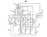
図2は、図1に示す全体構成図の一例を示す図である。なお、本発明は表示装置に関するものであるが、ここでは、表示装置の一例として有機表示装置を例にして説明する。表示装置内には、画素として、基準素子10と表示素子11がある。 FIG. 2 is a diagram showing an example of the overall configuration diagram shown in FIG. Although the present invention relates to a display device, an organic display device will be described here as an example of the display device. In the display device, there are a
基準素子10は、検出時にのみ使用する素子で、使用頻度を少なくし、素子劣化を抑えた状態で検出比較の基準とする。表示素子11は、駆動時には常時使用する素子である。検出は、この2つの素子を比較し、その差から素子の状態を求めるもので、その結果から表示制御部17で補正量を演算し、表示素子11にフィードバックする。 The
なお、図2において、基準素子10を設けているが、検出構成によっては、表示素子11を基準素子に割り当てることもできる。表示素子11の駆動電源は、検出時と表示時とで独立した形態をもつ。検出時には、検出用電流源12を用い、表示時には、表示用電圧源13を用いる。検出用電流源12と基準素子10とはスイッチ14で接続されている。スイッチ15は表示時にオンになるものである。検出用電流源12と表示素子11とはスイッチ16で接続されている。ここで、スイッチ15とスイッチ16は同時にオンになることはない。 Although the
表示制御部17は、各スイッチや電源の制御及び検出と補正を行う。シフトレジスタ18は、スイッチ16を制御するものである。このシフトレジスタ18は、表示制御部17の中に組み込まれても、独立した制御部として配置されても構わないが、制御は表示制御部17が行う。 The
信号線19は、表示時と検出時の両方で用いる共用線である。信号線19に接続されているスイッチ15は、表示制御部17が制御する制御信号21で制御され、スイッチ15は、表示制御部17が制御する制御信号22で制御される。 The
スイッチ14とスイッチ24がオンの時、保持部23は、基準素子10の電圧を保持し、この値を基準電圧として、基準線60に出力する。検出部25は、基準線60から入力されるデータと検出線20から入力されるデータとを比較し、その比較結果を表示制御部17に出力する。この比較には、データが電圧として検出されるので、コンパレータ等を使用することができる。また、比較結果が微小の場合、検出部にアンプを設けて検出電圧を増幅し、検出精度を上げることもできる。 When the
なお、表示用電圧源13と表示素子11とは画素制御部26で接続されている。また、検出用電流源12と表示用電圧源13のように電源を別々に設けているが、検出構成によっては、電流源又は電圧源のどちらかの電源にまとめてもよい。信号線19と表示素子11とは、スイッチ27で接続される。スイッチ27は、表示制御部17が制御するモード選択信号28で制御する。 The
図3は、図2の構成で信号線19の周辺について、更に詳細に表した構成例であり、表示時の状態を示している。画素29は、表示素子11、画素制御部26、モード切替スイッチ27から構成される。モード切替スイッチ27はモード選択信号28で制御する。スイッチ15は、表示制御部17が制御する制御信号21で制御する。スイッチ16は、表示制御部17が制御する制御信号22で制御する。 FIG. 3 is a configuration example showing the periphery of the
また、本実施例では、R、G、Bを時分割で制御する構成になっている。信号線19とRGB各画素とは、R選択スイッチ30、G選択スイッチ31、B選択スイッチ32で接続する。R選択スイッチ30はR選択信号33で制御する。G選択スイッチ31はG選択信号34で制御する。B選択スイッチ32はB選択信号35で制御する。Rの各画素とR選択スイッチ30は信号線36で接続する。Gの各画素とG選択スイッチ31は信号線37で接続する。Bの各画素とB選択スイッチ32は信号線38で接続する。モード選択信号28、R選択信号33、G選択信号34、B選択信号35は表示制御部17で制御しても、他の独立した回路で制御してもよい。 In this embodiment, R, G, and B are controlled in a time-sharing manner. The
次に、図3の動作を説明する。表示時には、表示制御部17からの制御信号21と制御信号22によって、スイッチ15がオン、スイッチ16がオフになる。この状態で信号線19には、表示制御部17からのデータが供給される。 Next, the operation of FIG. 3 will be described. At the time of display, the
そして、Rの表示時は、時分割制御されたR選択スイッチ30がオン、G選択スイッチ31がオフ、B選択スイッチ32がオフ、モード切替スイッチ28がオフの状態で、表示制御部17からのデータにより、画素制御部26が表示用電圧源13からの電圧を制御して表示素子11に電圧を印加して、表示素子11を発光させる。 At the time of displaying R, the
同様に、Gの表示時は、時分割制御されたG選択スイッチ31がオン、R選択スイッチ30がオフ、B選択スイッチ32がオフ、モード切替スイッチ27がオフの状態で、表示制御部17からのデータにより、画素制御部26が表示用電圧源13からの電圧を制御して表示素子11に電圧を印加して、表示素子11を発光させる。 Similarly, at the time of displaying G, the
また、Bの表示時は、時分割制御されたB選択スイッチ32がオン、R選択スイッチ30がオフ、G選択スイッチ31がオフ、モード切替スイッチ27がオフの状態で、表示制御部17からのデータにより、画素制御部26が表示用電圧源13からの電圧を制御して表示素子11に電圧を印加して、表示素子11を発光させる。このように、各スイッチを制御して順次表示素子を発光させる。 Further, when B is displayed, the time-division-controlled
図4は、図3と同様の構成で検出時の動作を示している。検出時には、表示制御部17からの制御信号21と制御信号22によって、スイッチ15がオフ、スイッチ16がオンになる。この状態で信号線19は検出線20と接続される。検出時には、表示素子11の状態を読み出す必要があるので、画素制御部26は表示用電圧源13からの電圧を遮断する。検出対象の画素については、モード切替スイッチ27をオンにすることで、表示素子11を信号線19に接続する。 FIG. 4 shows an operation at the time of detection with the same configuration as FIG. At the time of detection, the
Rの画素を検出するには、R選択スイッチ30をオンにし、検出画素のモード切替スイッチ27をオンにする。検出線には、検出用電流源12が接続されており、表示素子11の特性によって信号線19には一定の電圧が生じ、表示素子11の状態が検出線20に表れる。 In order to detect the R pixel, the
同様に、Gの画素を検出するには、G選択スイッチ31をオンにし、検出画素のモード切替スイッチ27をオンにすることで、表示素子11の状態が検出線20に表れる。 Similarly, in order to detect the G pixel, the state of the display element 11 appears on the
また、Bの画素を検出するには、B選択スイッチ32をオンにし、検出画素のモード切替スイッチ27をオンにすることで表示素子11の状態が検出線20に表れる。 Further, in order to detect the B pixel, the state of the display element 11 appears on the
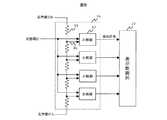
図5は、検出線と表示素子に関する一構成例である。この構成では、電流源と基準素子を設け、その基準素子と表示素子とを比較する。図5において、基準線60は、基準電圧を保持する保持部23と接続する。検出線61には、電流源62が接続されている。表示素子50、表示素子51、表示素子52、その他全ての表示素子が、スイッチ63に接続され、基準素子55がスイッチ64に接続され、保持部23が、スイッチ65に接続されている。スイッチ63、スイッチ64、スイッチ65は、表示制御部17で制御する。 FIG. 5 is an example of a configuration related to the detection line and the display element. In this configuration, a current source and a reference element are provided, and the reference element and the display element are compared. In FIG. 5, the
次に、図5の動作を説明する。表示制御部17は、スイッチ64とスイッチ65をオンにし、スイッチ63を全てオフにする。この状態で、電流源62と基準素子55が接続され、その時の電圧を保持部23に保持する。以後、表示制御部17の制御により、検出の1サイクルが終わるまで、保持部23はこの値を保持し、基準線60にその値を出力し続ける。 Next, the operation of FIG. 5 will be described. The
基準素子55の処理が終わると、表示制御部17はシフトレジスタ18を使用し、スイッチ63で表示素子50を検出線61に接続する。検出部25は基準線60と検出線61からの電圧の比較を行い、その結果を表示制御部17に出力する。表示制御部17は検出部25から結果が入力されたら、シフトレジスタ18で表示素子51をスイッチ63で検出線61に接続する。そして、検出部25は基準線60と検出線61からの電圧の比較を行い、その結果を表示制御部17に出力する。このように、基準素子55を基準として表示素子を比較する。 When the processing of the
図6は、図5に示す検出部25の構成例を示している。図6において、基準電圧Aと基準電圧Bは、その一方を図5に示す基準線60の値とし、もう一方をこの基準線60の値にオフセット値を加算又は減算して求めた値とする。基準電圧A及び基準電圧Bと、図5に示す検出線61からの状態電圧とを比較する。比較に用いる基準値94は基準電圧Aと基準電圧Bを抵抗ラダーで分割した値とする。比較器95は、状態電圧と基準値94を比較し、その結果を表示制御部17へ出力する。 FIG. 6 shows a configuration example of the
本実施例では、比較器95が4個の構成になっているが、この個数及び抵抗ラダー93の分割数は、比較精度に応じて増減させながら決定する。比較器95で得られた検出結果は表示制御部17で処理され、入力表示データを補正して表示素子にフィードバックされる。 In this embodiment, the number of the
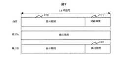
図7は、検出のタイミングを示している。図7において、通常では、1水平期間には表示期間100と帰線期間101がある。検出Aでは、表示期間100と帰線期間101を全て検出に用いて全画素を検出する。この場合、検出中は表示を一切行わない。検出Bでは、表示期間100はそのままとし、帰線期間101の全部又は一部を検出期間102に割り当てる。この場合、表示しながらの検出になるため、検出Aに対して、1画面全てを検出するのに時間がかかるが、表示期間に対しては影響ない。 FIG. 7 shows the detection timing. In FIG. 7, normally, there are a
図8は、表示制御部における処理を示すフローチャートである。処理110で検出処理が開始されると、処理111で垂直カウンタをリセットする。処理112において検出期間であるかを判定し、検出期間になると処理113において基準電圧を測定し、処理114において処理113の結果である基準電圧を保持部で保持する。処理115で各画素を切り替えるシフトレジスタをセットし、処理116で対象画素の状態を検出する。処理117で検出部からの応答を待機する。検出部で検出されると処理118で検出状態を判定し、検出できなかった場合、処理119でエラー処理をする。処理118で正常に検出されると処理120で1ラインの検出が終了したか判定し、1ラインの途中であれば処理121でシフトレジスタをシフトさせ、残りを検出する。処理120で1ラインの検出が終了すると、処理122で補正処理を実施する。処理123で1画面の検出が終了したか判定し、1画面の途中であれば垂直カウンタをカウントアップし、残りを検出する。処理123で1画面の検出が終了すると、処理125で検出を終了する。 FIG. 8 is a flowchart showing processing in the display control unit. When the detection process is started in
図9は、実施例1の図5に関しての別構成をとる実施例である。この構成は、基準素子を複数まとめて検出する。基準素子をn個用意すると、検出する表示素子はn個となる。また、1個を検出する場合と比較して、電流源の電流供給量をn倍とすることで、検出精度がn倍になる。 FIG. 9 is an embodiment having another configuration related to FIG. 5 of the first embodiment. In this configuration, a plurality of reference elements are detected together. If n reference elements are prepared, n display elements are detected. In addition, the detection accuracy is increased by n times by increasing the current supply amount of the current source by n times compared to the case of detecting one.
図9において、基準線60は基準電圧を保持する保持部23と接続する。検出線61には、共通の電流源62が接続されている。表示素子A50、表示素子B51、表示素子C52、表示素子D53、その他全ての画素がスイッチ63で接続され、基準素子A56と基準素子B57がスイッチ64で接続され、保持部23がスイッチ65で接続されている。スイッチ63、スイッチ64、スイッチ65は表示制御部17で制御する。 In FIG. 9, a
次に、図9の動作を説明する。表示制御部17は、スイッチ64とスイッチ65をオンにし、スイッチ63を全てオフにする。この状態で、電流源62と基準素子A56と基準素子B57が接続され、その時の電圧を保持部23に保持する。以後、表示制御部17の制御により、検出の1サイクルが終わるまで、保持部23はこの値を保持し、基準線60にその値を出力し続ける。 Next, the operation of FIG. 9 will be described. The
本実施例では、基準素子が2個であるので、基準素子の特性が同等であれば電流源62の電流は半分ずつ基準素子に流れる。また、特性が異なった場合は、平均特性になる。基準素子の処理が終わると、表示制御部17はシフトレジスタ18を使用し、スイッチ63で表示素子A50及び表示素子B51を検出線61に接続する。検出量は各画素の平均量になる。検出部25は、基準線60と検出線61からの電圧の比較を行い、その比較結果を表示制御部17に出力する。表示制御部17は、検出部25から結果が入力されたら、シフトレジスタ18で表示素子C52及び表示素子D53をスイッチ63で検出線61に接続する。次に、検出部25は、基準線60と検出線61からの電圧の比較を行い、その比較結果を表示制御部17に出力する。このようにして、複数画素をまとめた場合の比較検出をする。 In this embodiment, since there are two reference elements, if the characteristics of the reference elements are the same, the current of the
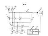
図10は、実施例1の図5に関しての別構成をとる実施例である。この構成では表示素子以外に基準素子を設けず、電流源を2つ設け、隣同士の表示素子を比較し、表示素子間での均衡を保つ構成である。基準線40及び検出線41にはスイッチ42とスイッチ43とで全ての表示素子が接続できる。また、電流源を基準線40と検出線41にそれぞれ電流源44と電流源45として独立して設ける。スイッチ42とスイッチ43は制御部17で制御する。 FIG. 10 is an embodiment having another configuration with respect to FIG. 5 of the first embodiment. In this configuration, the reference element is not provided other than the display element, two current sources are provided, the display elements adjacent to each other are compared, and the balance between the display elements is maintained. All display elements can be connected to the
次に、図10の動作を説明する。表示素子の状態を検出する場合は、表示素子A50と表示素子B51、表示素子B51と表示素子C52の順で比較する。表示素子A50をスイッチ42で基準線40に接続し、表示素子B51をスイッチ43で検出線41に接続する。検出部25は、基準線40と検出線41からの電圧の比較を行い、その結果を表示制御部17に出力する。表示制御部17は、検出部25から結果が入力されたら、表示素子B51をスイッチ42で基準線40に接続し、表示素子C52をスイッチ43で検出線41に接続する。次に、検出部25は、基準線40と検出線41からの電圧の比較を行い、その結果を表示制御部17に出力する。このように隣接する表示素子同士を比較する。比較の結果、差のある表示素子への入力表示データについて補正を行う。 Next, the operation of FIG. 10 will be described. When detecting the state of the display element, the display element A50 and the display element B51, and the display element B51 and the display element C52 are compared in this order. The display element A50 is connected to the
図11は、実施例1の図5に関しての別構成をとる実施例である。この構成では表示素子以外に基準素子を設けず、電流源を2つ設け、表示素子の1つを基準素子として設定し、他の表示素子を比較する。 FIG. 11 is an embodiment having another configuration with respect to FIG. 5 of the first embodiment. In this configuration, the reference element is not provided other than the display element, two current sources are provided, one of the display elements is set as the reference element, and the other display elements are compared.
図11において、基準線40には表示素子の1つを代表として接続する。基準線40には表示素子A50と電流源44を接続している。本実施例では、基準線40に1つの表示素子しか接続していないが、複数の表示素子をスイッチで選択して基準線40に接続できるようにした方がよい。表示素子B51、表示素子C52、表示素子D53はスイッチ43で検出線41に接続する。検出線41には電流源45が接続されている。 In FIG. 11, one reference element is connected to the
次に、図11の動作を説明する。表示素子の状態を検出する場合は、表示素子A50と表示素子B51、表示素子A50と表示素子C52、表示素子A50と表示素子D53の順で比較する。表示素子A50を基準線40に固定接続し、表示素子B51をスイッチ43で検出線41に接続する。検出部25は、基準線40と検出線41からの電圧の比較を行い、その結果を表示制御部17に出力する。表示制御部17は、検出部25から結果が入力されたら、表示素子C52をスイッチ43で検出線41に接続する。次に、検出部25は、基準線40と検出線41からの電圧の比較を行い、その結果を表示制御部17に出力する。このように表示素子A50を基準として他の表示素子を比較する。 Next, the operation of FIG. 11 will be described. When detecting the state of the display element, the display element A50 and the display element B51, the display element A50 and the display element C52, and the display element A50 and the display element D53 are compared in this order. The display element A50 is fixedly connected to the
図12は、実施例1の図5に関しての別構成をとる実施例である。この構成では電流源を2つ設け、基準素子と表示素子を比較する。基準線40には基準素子55と電流源44が接続されている。本実施例では、基準線40に基準素子を1つしか接続していないが、数個の基準素子をスイッチで選択して基準線40に接続できるようにした方がよい。表示素子A50、表示素子B51、表示素子C52は、スイッチ43で検出線41に接続する。検出線41には電流源45が接続されている。 FIG. 12 is an example in which another configuration with respect to FIG. In this configuration, two current sources are provided, and the reference element and the display element are compared. A
次に、図12の動作を説明する。基準素子と表示素子の状態を検出する場合は、基準素子55と表示素子A50、基準素子55と表示素子B51、基準素子55と表示素子C52の順で比較する。基準素子55を基準線40に固定接続し、表示素子A50をスイッチ43で検出線41に接続する。検出部25は、基準線40と検出線41からの電圧の比較を行い、その結果を表示制御部17に出力する。表示制御部17は、検出部25から結果が入力されたら、表示素子B51をスイッチ43で検出線41に接続する。次に、検出部25は、基準線40と検出線41からの電圧の比較を行い、その結果を表示制御部17に出力する。このように基準素子55を基準として表示素子を比較する。 Next, the operation of FIG. 12 will be described. When detecting the state of the reference element and the display element, the
図13は、実施例1の図5に関しての別構成をとる実施例である。この構成では、電流源46を、抵抗47を通した基準線40と、抵抗48を通した検出線41で共通で使用する。基準線40には、基準素子55と抵抗47を通して電流源46を接続している。 FIG. 13 is an embodiment having another configuration with respect to FIG. 5 of the first embodiment. In this configuration, the
本実施例では、基準線40に基準素子を1つしか接続していないが、複数の基準素子をスイッチで選択して基準線40に接続できるようにした方がよい。表示素子A50、表示素子B51、表示素子C52は、スイッチ43で検出線41に接続する。検出線41には抵抗48を通して電流源46が接続されている。 In the present embodiment, only one reference element is connected to the
次に、図13の動作を説明する。基準素子と表示素子とを検出する場合は、基準素子55と表示素子A50、基準素子55と表示素子B51、基準素子55と表示素子C52の順で比較する。基準素子55を基準線40に固定接続し、表示素子A50をスイッチ43で検出線41に接続する。 Next, the operation of FIG. 13 will be described. When detecting the reference element and the display element, the
電流源46が共通していることから、基準素子55と表示素子A50が等しくなければ、基準線40と検出線41との間には微小電圧差が生じる。基準素子55と表示素子A50が等しい場合は、基準線40と検出線41の間には電圧差は生じない。検出部25は、基準線40と検出線41からの電圧の比較を行い、その結果を表示制御部17に出力する。表示制御部17は、検出部25から結果が入力されたら、表示素子B51をスイッチ43で検出線41に接続する。次に、検出部25は、基準線40と検出線41からの電圧の比較を行い、その結果を表示制御部17に出力する。このように基準素子55を基準として表示素子を比較する。 Since the
図14は、実施例1の図5に関しての別構成をとる実施例である。この構成では、電流源の代わりに電圧源を用いて、基準素子と表示素子のアノードを電圧源に接続した。この電圧源と定抵抗で基準素子と表示素子動作させる。基準線70には、基準素子85と抵抗72が接続される。検出線71には、抵抗73が接続されている。表示素子A80、表示素子B81、表示素子C82、その他全ての表示素子が、スイッチ74で接続される。スイッチ74は表示制御部17で制御する。 FIG. 14 shows an embodiment having another configuration with respect to FIG. In this configuration, a voltage source is used instead of the current source, and the reference element and the anode of the display element are connected to the voltage source. The reference element and the display element are operated with this voltage source and constant resistance. A
次に、図14の動作を説明する。基準線70には、電圧源に直列に接続された基準素子85と抵抗72との接続点に基準電圧が表れる。基準素子と表示素子とを検出する場合は、基準素子85と表示素子A80、基準素子85と表示素子B81、基準素子85と表示素子C82の順で比較する。表示制御部17により表示素子A80をスイッチ74で検出線71に接続する。検出部25は、基準線70と検出線71からの電圧の比較を行い、その結果を表示制御部17に出力する。表示制御部17は、検出部25から結果が入力されたら、表示素子B81をスイッチ74で検出線71に接続する。次に、検出部25は、基準線70と検出線71からの電圧の比較を行い、その結果を表示制御部17に出力する。このように、基準素子85を基準として表示素子を比較する。 Next, the operation of FIG. 14 will be described. In the
1…ドライバ、2…表示部、3…表示制御部、4…検出スイッチ、5…検出部、6…検出用電源、7…表示用電源、8…表示素子、9…画素制御部、10…基準素子、11…表示素子、12…検出用電源、13…表示用電源、17…表示制御部、18…シフトレジスタ部、23…保持部、25…検出部DESCRIPTION OF SYMBOLS 1 ... Driver, 2 ... Display part, 3 ... Display control part, 4 ... Detection switch, 5 ... Detection part, 6 ... Detection power supply, 7 ... Display power supply, 8 ... Display element, 9 ... Pixel control part, 10 ... Reference element 11 ...
Claims (12)
Translated fromJapanese前記信号線への表示データの入力と表示素子の状態の出力とを切り替える検出スイッチと、前記検出スイッチに接続された検出用電源と、前記検出スイッチからの表示素子の状態を検出する検出部とを備え、
前記表示素子の状態を信号線と検出スイッチとを介して検出部に入力することを特徴とする表示装置A display unit comprising a plurality of display elements, a pixel control unit for controlling the light emission amount of the display element according to display data, and a display power source connected to the pixel control unit, and display data on the display element of the display unit And an image display device having a signal line for outputting the state of the display element.
A detection switch for switching input of display data to the signal line and output of a state of the display element, a detection power source connected to the detection switch, and a detection unit for detecting the state of the display element from the detection switch; With
A display device, wherein the state of the display element is input to a detection unit via a signal line and a detection switch
Priority Applications (2)
| Application Number | Priority Date | Filing Date | Title |
|---|---|---|---|
| JP2006286193AJP2008102404A (en) | 2006-10-20 | 2006-10-20 | Display device |
| US11/874,961US20080150845A1 (en) | 2006-10-20 | 2007-10-19 | Display device |
Applications Claiming Priority (1)
| Application Number | Priority Date | Filing Date | Title |
|---|---|---|---|
| JP2006286193AJP2008102404A (en) | 2006-10-20 | 2006-10-20 | Display device |
Publications (1)
| Publication Number | Publication Date |
|---|---|
| JP2008102404Atrue JP2008102404A (en) | 2008-05-01 |
Family
ID=39436756
Family Applications (1)
| Application Number | Title | Priority Date | Filing Date |
|---|---|---|---|
| JP2006286193APendingJP2008102404A (en) | 2006-10-20 | 2006-10-20 | Display device |
Country Status (2)
| Country | Link |
|---|---|
| US (1) | US20080150845A1 (en) |
| JP (1) | JP2008102404A (en) |
Cited By (14)
| Publication number | Priority date | Publication date | Assignee | Title |
|---|---|---|---|---|
| WO2009087746A1 (en)* | 2008-01-07 | 2009-07-16 | Panasonic Corporation | Display device, electronic device and driving method |
| JP2009175652A (en)* | 2008-01-21 | 2009-08-06 | Samsung Mobile Display Co Ltd | Organic electroluminescent display device and driving method thereof |
| JP2009244654A (en)* | 2008-03-31 | 2009-10-22 | Casio Comput Co Ltd | Display device and method for controlling driving of the same |
| JP2009294371A (en)* | 2008-06-04 | 2009-12-17 | Hitachi Displays Ltd | Image display apparatus |
| WO2010001590A1 (en)* | 2008-07-04 | 2010-01-07 | パナソニック株式会社 | Display device and method for controlling the same |
| WO2010001594A1 (en)* | 2008-07-04 | 2010-01-07 | パナソニック株式会社 | Display device and control method thereof |
| JP2010039407A (en)* | 2008-08-08 | 2010-02-18 | Hitachi Displays Ltd | Display device |
| JP2010169991A (en)* | 2009-01-26 | 2010-08-05 | Hitachi Displays Ltd | Display device |
| JP2010530993A (en)* | 2007-06-22 | 2010-09-16 | イーストマン コダック カンパニー | OLED display with degradation and efficiency compensation |
| JP2011523720A (en)* | 2008-05-29 | 2011-08-18 | グローバル・オーエルイーディー・テクノロジー・リミテッド・ライアビリティ・カンパニー | Compensation method for multi-color electroluminescent display |
| JP2012042453A (en)* | 2010-08-20 | 2012-03-01 | Samsung Electro-Mechanics Co Ltd | Deterioration detector for display device |
| JP2013512473A (en)* | 2009-11-30 | 2013-04-11 | イグニス・イノベイション・インコーポレーテッド | Time-varying correction system and method in AMOLED display |
| US9311859B2 (en) | 2009-11-30 | 2016-04-12 | Ignis Innovation Inc. | Resetting cycle for aging compensation in AMOLED displays |
| US9384698B2 (en) | 2009-11-30 | 2016-07-05 | Ignis Innovation Inc. | System and methods for aging compensation in AMOLED displays |
Families Citing this family (48)
| Publication number | Priority date | Publication date | Assignee | Title |
|---|---|---|---|---|
| CA2443206A1 (en) | 2003-09-23 | 2005-03-23 | Ignis Innovation Inc. | Amoled display backplanes - pixel driver circuits, array architecture, and external compensation |
| US10012678B2 (en) | 2004-12-15 | 2018-07-03 | Ignis Innovation Inc. | Method and system for programming, calibrating and/or compensating, and driving an LED display |
| US8576217B2 (en) | 2011-05-20 | 2013-11-05 | Ignis Innovation Inc. | System and methods for extraction of threshold and mobility parameters in AMOLED displays |
| US10013907B2 (en) | 2004-12-15 | 2018-07-03 | Ignis Innovation Inc. | Method and system for programming, calibrating and/or compensating, and driving an LED display |
| TWI402790B (en) | 2004-12-15 | 2013-07-21 | Ignis Innovation Inc | Method and system for programming, calibrating and driving a light-emitting element display |
| US9799246B2 (en) | 2011-05-20 | 2017-10-24 | Ignis Innovation Inc. | System and methods for extraction of threshold and mobility parameters in AMOLED displays |
| JP5355080B2 (en) | 2005-06-08 | 2013-11-27 | イグニス・イノベイション・インコーポレーテッド | Method and system for driving a light emitting device display |
| CA2518276A1 (en) | 2005-09-13 | 2007-03-13 | Ignis Innovation Inc. | Compensation technique for luminance degradation in electro-luminance devices |
| TW200746022A (en) | 2006-04-19 | 2007-12-16 | Ignis Innovation Inc | Stable driving scheme for active matrix displays |
| CA2556961A1 (en) | 2006-08-15 | 2008-02-15 | Ignis Innovation Inc. | Oled compensation technique based on oled capacitance |
| JP2009069421A (en)* | 2007-09-12 | 2009-04-02 | Hitachi Displays Ltd | Display device |
| JP2009294376A (en)* | 2008-06-04 | 2009-12-17 | Hitachi Displays Ltd | Image display apparatus |
| US10319307B2 (en) | 2009-06-16 | 2019-06-11 | Ignis Innovation Inc. | Display system with compensation techniques and/or shared level resources |
| CA2669367A1 (en) | 2009-06-16 | 2010-12-16 | Ignis Innovation Inc | Compensation technique for color shift in displays |
| US20110043541A1 (en)* | 2009-08-20 | 2011-02-24 | Cok Ronald S | Fault detection in electroluminescent displays |
| JP2011112711A (en)* | 2009-11-24 | 2011-06-09 | Hitachi Displays Ltd | Display device |
| US10996258B2 (en) | 2009-11-30 | 2021-05-04 | Ignis Innovation Inc. | Defect detection and correction of pixel circuits for AMOLED displays |
| US8803417B2 (en) | 2009-12-01 | 2014-08-12 | Ignis Innovation Inc. | High resolution pixel architecture |
| CA2692097A1 (en) | 2010-02-04 | 2011-08-04 | Ignis Innovation Inc. | Extracting correlation curves for light emitting device |
| US10163401B2 (en) | 2010-02-04 | 2018-12-25 | Ignis Innovation Inc. | System and methods for extracting correlation curves for an organic light emitting device |
| US9881532B2 (en) | 2010-02-04 | 2018-01-30 | Ignis Innovation Inc. | System and method for extracting correlation curves for an organic light emitting device |
| US10089921B2 (en) | 2010-02-04 | 2018-10-02 | Ignis Innovation Inc. | System and methods for extracting correlation curves for an organic light emitting device |
| US20140313111A1 (en) | 2010-02-04 | 2014-10-23 | Ignis Innovation Inc. | System and methods for extracting correlation curves for an organic light emitting device |
| US10176736B2 (en) | 2010-02-04 | 2019-01-08 | Ignis Innovation Inc. | System and methods for extracting correlation curves for an organic light emitting device |
| CA2696778A1 (en) | 2010-03-17 | 2011-09-17 | Ignis Innovation Inc. | Lifetime, uniformity, parameter extraction methods |
| US8513897B2 (en)* | 2010-10-01 | 2013-08-20 | Winstar Display Co., Ltd | OLED display with a current stabilizing device and its driving method |
| US8907991B2 (en) | 2010-12-02 | 2014-12-09 | Ignis Innovation Inc. | System and methods for thermal compensation in AMOLED displays |
| US9530349B2 (en) | 2011-05-20 | 2016-12-27 | Ignis Innovations Inc. | Charged-based compensation and parameter extraction in AMOLED displays |
| US9466240B2 (en) | 2011-05-26 | 2016-10-11 | Ignis Innovation Inc. | Adaptive feedback system for compensating for aging pixel areas with enhanced estimation speed |
| US9773439B2 (en) | 2011-05-27 | 2017-09-26 | Ignis Innovation Inc. | Systems and methods for aging compensation in AMOLED displays |
| US10089924B2 (en) | 2011-11-29 | 2018-10-02 | Ignis Innovation Inc. | Structural and low-frequency non-uniformity compensation |
| US9324268B2 (en) | 2013-03-15 | 2016-04-26 | Ignis Innovation Inc. | Amoled displays with multiple readout circuits |
| US8937632B2 (en) | 2012-02-03 | 2015-01-20 | Ignis Innovation Inc. | Driving system for active-matrix displays |
| US8922544B2 (en) | 2012-05-23 | 2014-12-30 | Ignis Innovation Inc. | Display systems with compensation for line propagation delay |
| US9336717B2 (en) | 2012-12-11 | 2016-05-10 | Ignis Innovation Inc. | Pixel circuits for AMOLED displays |
| US9786223B2 (en) | 2012-12-11 | 2017-10-10 | Ignis Innovation Inc. | Pixel circuits for AMOLED displays |
| EP3043338A1 (en) | 2013-03-14 | 2016-07-13 | Ignis Innovation Inc. | Re-interpolation with edge detection for extracting an aging pattern for amoled displays |
| DE112014002915B4 (en)* | 2013-06-21 | 2018-02-01 | Yazaki Corporation | display device |
| CN105474296B (en) | 2013-08-12 | 2017-08-18 | 伊格尼斯创新公司 | A method and device for driving a display using image data |
| US9741282B2 (en) | 2013-12-06 | 2017-08-22 | Ignis Innovation Inc. | OLED display system and method |
| US9761170B2 (en) | 2013-12-06 | 2017-09-12 | Ignis Innovation Inc. | Correction for localized phenomena in an image array |
| US9502653B2 (en) | 2013-12-25 | 2016-11-22 | Ignis Innovation Inc. | Electrode contacts |
| DE102015206281A1 (en) | 2014-04-08 | 2015-10-08 | Ignis Innovation Inc. | Display system with shared level resources for portable devices |
| CA2879462A1 (en) | 2015-01-23 | 2016-07-23 | Ignis Innovation Inc. | Compensation for color variation in emissive devices |
| CA2889870A1 (en) | 2015-05-04 | 2016-11-04 | Ignis Innovation Inc. | Optical feedback system |
| CA2892714A1 (en) | 2015-05-27 | 2016-11-27 | Ignis Innovation Inc | Memory bandwidth reduction in compensation system |
| CA2900170A1 (en) | 2015-08-07 | 2017-02-07 | Gholamreza Chaji | Calibration of pixel based on improved reference values |
| US11645973B1 (en)* | 2022-02-28 | 2023-05-09 | Sct Ltd. | Programmable electrode voltage swing reduction apparatus and method |
Family Cites Families (6)
| Publication number | Priority date | Publication date | Assignee | Title |
|---|---|---|---|---|
| WO2003034384A2 (en)* | 2001-10-19 | 2003-04-24 | Clare Micronix Integrated Systems, Inc. | Method and system for precharging oled/pled displays with a precharge latency |
| US6806497B2 (en)* | 2002-03-29 | 2004-10-19 | Seiko Epson Corporation | Electronic device, method for driving the electronic device, electro-optical device, and electronic equipment |
| EP1383103B1 (en)* | 2002-07-19 | 2012-03-21 | St Microelectronics S.A. | Automatic adaptation of the supply voltage of an electroluminescent panel depending on the desired luminance |
| US6885873B2 (en)* | 2002-12-19 | 2005-04-26 | Intel Corporation | Adaptively extending tunable range of frequency in a closed loop |
| US8013809B2 (en)* | 2004-06-29 | 2011-09-06 | Semiconductor Energy Laboratory Co., Ltd. | Display device and driving method of the same, and electronic apparatus |
| US8207914B2 (en)* | 2005-11-07 | 2012-06-26 | Global Oled Technology Llc | OLED display with aging compensation |
- 2006
- 2006-10-20JPJP2006286193Apatent/JP2008102404A/enactivePending
- 2007
- 2007-10-19USUS11/874,961patent/US20080150845A1/ennot_activeAbandoned
Cited By (27)
| Publication number | Priority date | Publication date | Assignee | Title |
|---|---|---|---|---|
| KR101243353B1 (en) | 2007-06-22 | 2013-03-13 | 글로벌 오엘이디 테크놀러지 엘엘씨 | Oled display with aging and efficiency compensation |
| JP2010530993A (en)* | 2007-06-22 | 2010-09-16 | イーストマン コダック カンパニー | OLED display with degradation and efficiency compensation |
| US8164546B2 (en) | 2008-01-07 | 2012-04-24 | Panasonic Corporation | Display device, electronic device, and driving method |
| JP5254998B2 (en)* | 2008-01-07 | 2013-08-07 | パナソニック株式会社 | Display device and driving method |
| WO2009087746A1 (en)* | 2008-01-07 | 2009-07-16 | Panasonic Corporation | Display device, electronic device and driving method |
| US8355016B2 (en) | 2008-01-07 | 2013-01-15 | Panasonic Corporation | Display device, electronic device, and driving method |
| US8791939B2 (en) | 2008-01-07 | 2014-07-29 | Panasonic Corporation | Display device, electronic device, and driving method |
| JP2009175652A (en)* | 2008-01-21 | 2009-08-06 | Samsung Mobile Display Co Ltd | Organic electroluminescent display device and driving method thereof |
| JP2009244654A (en)* | 2008-03-31 | 2009-10-22 | Casio Comput Co Ltd | Display device and method for controlling driving of the same |
| JP2011523720A (en)* | 2008-05-29 | 2011-08-18 | グローバル・オーエルイーディー・テクノロジー・リミテッド・ライアビリティ・カンパニー | Compensation method for multi-color electroluminescent display |
| JP2009294371A (en)* | 2008-06-04 | 2009-12-17 | Hitachi Displays Ltd | Image display apparatus |
| US8089477B2 (en) | 2008-07-04 | 2012-01-03 | Panasonic Corporation | Display device and method for controlling the same |
| CN101960509B (en)* | 2008-07-04 | 2015-04-15 | 松下电器产业株式会社 | Display device and control method thereof |
| JP4972209B2 (en)* | 2008-07-04 | 2012-07-11 | パナソニック株式会社 | Display device and control method thereof |
| JP5010030B2 (en)* | 2008-07-04 | 2012-08-29 | パナソニック株式会社 | Display device and control method thereof |
| JP2012190023A (en)* | 2008-07-04 | 2012-10-04 | Panasonic Corp | Display device and control method therefor |
| KR101537829B1 (en)* | 2008-07-04 | 2015-07-17 | 가부시키가이샤 제이올레드 | Display device and control method thereof |
| WO2010001594A1 (en)* | 2008-07-04 | 2010-01-07 | パナソニック株式会社 | Display device and control method thereof |
| US8890778B2 (en) | 2008-07-04 | 2014-11-18 | Panasonic Corporation | Display device and method for controlling the same |
| WO2010001590A1 (en)* | 2008-07-04 | 2010-01-07 | パナソニック株式会社 | Display device and method for controlling the same |
| US8547307B2 (en) | 2008-07-04 | 2013-10-01 | Panasonic Corporation | Display device and method for controlling the same |
| JP2010039407A (en)* | 2008-08-08 | 2010-02-18 | Hitachi Displays Ltd | Display device |
| JP2010169991A (en)* | 2009-01-26 | 2010-08-05 | Hitachi Displays Ltd | Display device |
| JP2013512473A (en)* | 2009-11-30 | 2013-04-11 | イグニス・イノベイション・インコーポレーテッド | Time-varying correction system and method in AMOLED display |
| US9311859B2 (en) | 2009-11-30 | 2016-04-12 | Ignis Innovation Inc. | Resetting cycle for aging compensation in AMOLED displays |
| US9384698B2 (en) | 2009-11-30 | 2016-07-05 | Ignis Innovation Inc. | System and methods for aging compensation in AMOLED displays |
| JP2012042453A (en)* | 2010-08-20 | 2012-03-01 | Samsung Electro-Mechanics Co Ltd | Deterioration detector for display device |
Also Published As
| Publication number | Publication date |
|---|---|
| US20080150845A1 (en) | 2008-06-26 |
Similar Documents
| Publication | Publication Date | Title |
|---|---|---|
| JP2008102404A (en) | Display device | |
| JP5449641B2 (en) | Display device | |
| JP5984398B2 (en) | Light emitting device and control method thereof | |
| KR100624136B1 (en) | Organic electroluminescent display with auto-brightness control | |
| US6376994B1 (en) | Organic EL device driving apparatus having temperature compensating function | |
| US8106902B2 (en) | Display device | |
| US20060214888A1 (en) | Method and circuit arrangement for the ageing compensation of an organic light-emitting diode and circuit arrangement | |
| JP6290610B2 (en) | Display device | |
| US20130027438A1 (en) | Display capable of calibrating white balance and method thereof | |
| JP2008292649A (en) | Image display device | |
| JP2009025735A (en) | Image display device | |
| JP2009237200A (en) | Image display device | |
| KR102439194B1 (en) | Conroller, display device and method for controlling method thereof | |
| JP2007240803A (en) | Spontaneous light emission display device, black level correcting device and program | |
| US8264432B2 (en) | Display device | |
| JP2010169991A (en) | Display device | |
| JP2007240802A (en) | Spontaneous light emission display device, white balance adjusting device, and program | |
| JP6827733B2 (en) | Light emitting device and display device | |
| JP2010085807A (en) | Display device | |
| US20140292739A1 (en) | Organic light emitting display device and method for driving the same | |
| JP2001117535A (en) | Display element driving device | |
| CN110459159B (en) | Display device and driving method thereof | |
| KR20190016829A (en) | Organic light emitting display and controlling method for the same | |
| KR20120017714A (en) | Organic light emitting display device including current feedback circuit and driving method thereof | |
| JP2005134531A (en) | Display device and display method |
Legal Events
| Date | Code | Title | Description |
|---|---|---|---|
| A621 | Written request for application examination | Free format text:JAPANESE INTERMEDIATE CODE: A621 Effective date:20080409 | |
| A977 | Report on retrieval | Free format text:JAPANESE INTERMEDIATE CODE: A971007 Effective date:20080808 | |
| A131 | Notification of reasons for refusal | Free format text:JAPANESE INTERMEDIATE CODE: A131 Effective date:20081007 | |
| A521 | Request for written amendment filed | Free format text:JAPANESE INTERMEDIATE CODE: A523 Effective date:20081118 | |
| A131 | Notification of reasons for refusal | Free format text:JAPANESE INTERMEDIATE CODE: A131 Effective date:20090106 | |
| A521 | Request for written amendment filed | Free format text:JAPANESE INTERMEDIATE CODE: A523 Effective date:20090217 | |
| A02 | Decision of refusal | Free format text:JAPANESE INTERMEDIATE CODE: A02 Effective date:20090421 |