JP2008099224A - Amplifier, amplifying method, and filter - Google Patents
Amplifier, amplifying method, and filterDownload PDFInfo
- Publication number
- JP2008099224A JP2008099224AJP2006345074AJP2006345074AJP2008099224AJP 2008099224 AJP2008099224 AJP 2008099224AJP 2006345074 AJP2006345074 AJP 2006345074AJP 2006345074 AJP2006345074 AJP 2006345074AJP 2008099224 AJP2008099224 AJP 2008099224A
- Authority
- JP
- Japan
- Prior art keywords
- variable capacitance
- capacitance element
- switch
- voltage signal
- variable
- Prior art date
- Legal status (The legal status is an assumption and is not a legal conclusion. Google has not performed a legal analysis and makes no representation as to the accuracy of the status listed.)
- Pending
Links
- 238000000034methodMethods0.000titleclaimsabstractdescription21
- 230000003321amplificationEffects0.000claimsdescription55
- 238000003199nucleic acid amplification methodMethods0.000claimsdescription55
- 238000009825accumulationMethods0.000claimsdescription7
- 230000002238attenuated effectEffects0.000claimsdescription7
- 230000003068static effectEffects0.000claimsdescription5
- 230000003247decreasing effectEffects0.000claimsdescription4
- 230000005611electricityEffects0.000claimsdescription3
- 230000008859changeEffects0.000description61
- 238000010586diagramMethods0.000description42
- 230000007423decreaseEffects0.000description24
- 239000003990capacitorSubstances0.000description17
- 230000002441reversible effectEffects0.000description15
- 230000002829reductive effectEffects0.000description11
- 238000004519manufacturing processMethods0.000description6
- 230000007704transitionEffects0.000description5
- 239000004065semiconductorSubstances0.000description4
- 239000000758substrateSubstances0.000description4
- 238000006243chemical reactionMethods0.000description2
- 230000008034disappearanceEffects0.000description2
- 230000000694effectsEffects0.000description2
- 230000005684electric fieldEffects0.000description2
- 150000002500ionsChemical class0.000description2
- 229910044991metal oxideInorganic materials0.000description2
- 150000004706metal oxidesChemical class0.000description2
- 230000004048modificationEffects0.000description2
- 238000012986modificationMethods0.000description2
- 238000005070samplingMethods0.000description2
- 238000012546transferMethods0.000description2
- 230000009471actionEffects0.000description1
- 238000004891communicationMethods0.000description1
- 230000000295complement effectEffects0.000description1
- 238000012937correctionMethods0.000description1
- 238000005516engineering processMethods0.000description1
- 230000005669field effectEffects0.000description1
- 230000007246mechanismEffects0.000description1
- 230000003071parasitic effectEffects0.000description1
- 230000008569processEffects0.000description1
- 238000012545processingMethods0.000description1
- 238000004904shorteningMethods0.000description1
- 238000001228spectrumMethods0.000description1
Images


Landscapes
- Filters That Use Time-Delay Elements (AREA)
- Networks Using Active Elements (AREA)
- Amplifiers (AREA)
Abstract
Description
Translated fromJapanese本発明は、増幅器、増幅方法、およびフィルタに関する。 The present invention relates to an amplifier, an amplification method, and a filter.
近年、RF(Radio Frequency)回路とデジタル回路とをCMOS(Complementary Metal Oxide Semiconductor)の1チップに収めた無線通信用のSoC(System On Chip)において、高速クロックによる電流モードサンプリングやスイッチト・キャパシタ回路などのアナログ離散時間信号処理技術を用いて、RF回路を微細化および低消費電力化する技術が開発されている。 In recent years, in SoC (System On Chip) for wireless communication in which RF (Radio Frequency) circuit and digital circuit are housed in one chip of CMOS (Complementary Metal Oxide Semiconductor), current mode sampling by high speed clock and switched capacitor circuit A technique for miniaturizing an RF circuit and reducing power consumption has been developed using an analog discrete-time signal processing technique such as the above.
MOSFET(Metal Oxide Semiconductor Field effect transistor)で構成される離散時間パラメトリック増幅器(MOSFETパラメトリック増幅器)を用いて、RF回路の微細化および低消費電力化を図る技術としては、例えば、特許文献1が挙げられる。 As a technique for miniaturizing an RF circuit and reducing power consumption using a discrete-time parametric amplifier (MOSFET parametric amplifier) composed of a MOSFET (Metal Oxide Semiconductor Field Effect Transistor), for example,
しかしながら、上述した従来のMOSFETパラメトリック増幅器は、MOSFETパラメトリック増幅器に入力されるバイアス電圧と電圧信号とが重畳されたまま一緒に増幅されてしまう。したがって、MOSFETパラメトリック増幅器の出力信号が必要以上に高くなってしまい、当該出力信号を受け取る後段の構成要素は高い耐圧性を備えなければならないなど、当該出力信号の取り扱いが難しくなる。また、MOSFETパラメトリック増幅器の出力信号が必要以上に高くなると、回路の微細化や低消費電力化に適さなくなる。さらに、MOSFETパラメトリック増幅器の出力信号が、電源電圧よりも大きくなると、MOSFETの容量が低下して、当該出力信号の信号波形に歪みが生じてしまう。 However, the conventional MOSFET parametric amplifier described above is amplified together with the bias voltage and voltage signal input to the MOSFET parametric amplifier superimposed. Therefore, the output signal of the MOSFET parametric amplifier becomes unnecessarily high, and it is difficult to handle the output signal, for example, the subsequent components that receive the output signal must have high voltage resistance. Further, if the output signal of the MOSFET parametric amplifier becomes higher than necessary, it becomes unsuitable for circuit miniaturization and low power consumption. Further, when the output signal of the MOSFET parametric amplifier becomes larger than the power supply voltage, the capacity of the MOSFET is reduced, and the signal waveform of the output signal is distorted.
そこで、本発明は、上記問題に鑑みてなされたものであり、本発明の目的とするところは、増幅器に入力されるバイアス電圧と電圧信号とのうち、当該電圧信号を増幅することが可能な、新規かつ改良された増幅器、増幅方法、およびフィルタを提供することにある。 Accordingly, the present invention has been made in view of the above problems, and an object of the present invention is to amplify the voltage signal out of the bias voltage and the voltage signal input to the amplifier. It is an object to provide a new and improved amplifier, amplification method and filter.
上記目的を達成するために、本発明の第1の観点によれば、静電容量が可変する第1可変静電容量素子と、上記第1可変静電容量素子と電気的に接続され、上記第1可変静電容量素子と逆導電型であり、静電容量が可変する第2可変静電容量素子と、上記第1可変静電容量素子と上記第2可変静電容量素子とに対してバイアス電圧と電圧信号とを選択的に入力する第1入力部とを備え、上記第1可変静電容量素子と上記第2可変静電容量素子とに上記バイアス電圧と上記電圧信号とが入力される場合は、上記第1可変静電容量素子と上記第2可変静電容量素子との静電容量を第1の値とし、上記第1可変静電容量素子と上記第2の可変静電容量素子の静電容量を、上記第1の値よりも小さな第2の値として上記電圧信号を増幅する増幅器が提供される。 In order to achieve the above object, according to a first aspect of the present invention, a first variable capacitance element whose capacitance is variable, electrically connected to the first variable capacitance element, and A second variable capacitance element having a conductivity opposite to that of the first variable capacitance element and having a variable capacitance, and the first variable capacitance element and the second variable capacitance element. A first input unit that selectively inputs a bias voltage and a voltage signal, and the bias voltage and the voltage signal are input to the first variable capacitance element and the second variable capacitance element. The first variable capacitance element and the second variable capacitance element are set to a first value, and the first variable capacitance element and the second variable capacitance element are set to a first value. An amplifier is provided that amplifies the voltage signal by setting the capacitance of the element to a second value that is smaller than the first value. It is.
上記増幅器は、第1可変静電容量素子と、第2可変静電容量素子と、第1入力部とを備える。第1可変静電容量素子は静電容量が可変する。また、第2可変静電容量素子は、第1可変静電容量素子と逆導電型であり、静電容量が可変する。第1入力部は、第1可変静電容量素子と第2可変静電容量素子とに対してバイアス電圧と電圧信号とを選択的に入力する。第1可変静電容量素子と第2可変静電容量素子とは、上記バイアス電圧と上記電圧信号とが入力される場合には、静電容量を第1の値として、電荷を蓄える。そして、第1可変静電容量素子と第2可変静電容量素子とは、静電容量を上記第1の値よりも小さな第2の値へと減少させることにより、上記電圧信号を上記第2の値に対する上記第1の値の比倍に増幅した出力電圧信号を出力する。なお、上記バイアス電圧は、第1可変静電容量素子と第2可変静電容量素子とにおいて増幅分に相当する電荷が相殺されるため、実質的に増幅されない。 The amplifier includes a first variable capacitance element, a second variable capacitance element, and a first input unit. The first variable capacitance element has a variable capacitance. Further, the second variable capacitance element is of a conductivity type opposite to that of the first variable capacitance element, and the capacitance is variable. The first input unit selectively inputs a bias voltage and a voltage signal to the first variable capacitance element and the second variable capacitance element. When the bias voltage and the voltage signal are input, the first variable capacitance element and the second variable capacitance element store charges using the capacitance as the first value. The first variable capacitance element and the second variable capacitance element reduce the capacitance to a second value smaller than the first value, thereby causing the voltage signal to be changed to the second value. An output voltage signal amplified to the ratio of the first value to the value of is output. The bias voltage is not substantially amplified because the charge corresponding to the amount of amplification is canceled between the first variable capacitance element and the second variable capacitance element.
また上記バイアス電圧の増幅分をキャンセルするための電圧を、上記第1可変静電容量素子と上記第2可変静電容量素子とに印加するとしてもよい。 A voltage for canceling the amplification of the bias voltage may be applied to the first variable capacitance element and the second variable capacitance element.
上記第1可変静電容量素子と上記第2可変静電容量素子とに、例えば、電源電圧を印加することにより、増幅された上記バイアス電圧の増幅分に相当する電荷を相殺することができる。 By applying, for example, a power supply voltage to the first variable capacitance element and the second variable capacitance element, it is possible to cancel the charge corresponding to the amplified amount of the bias voltage.
また、上記第1可変静電容量素子と上記第2可変静電容量素子とは、例えば、MOSバラクタであり、上記第1入力部は、例えば、第1スイッチを備え、上記第1可変静電容量素子と上記第2可変静電容量素子とのゲート端子は、それぞれ上記第1スイッチと接続され、上記第1可変静電容量素子のソース端子とドレイン端子とは、例えば、第2スイッチを介して電源電圧を出力する電源、またはグランドに接続され、上記第2可変静電容量素子のソース端子とドレイン端子とは、例えば、第3スイッチを介して上記電源、またはグランドに接続され、上記第2スイッチが上記電源に接続される場合、上記第3スイッチはグランドに接続されて、上記第1可変静電容量素子と上記第2可変静電容量素子との静電容量を上記第1の値とし、上記第2スイッチがグランドに接続される場合、上記第3スイッチは上記電源に接続されて、上記第1可変静電容量素子と上記第2可変静電容量素子との静電容量を上記第2の値とするとしてもよい。 Further, the first variable capacitance element and the second variable capacitance element are, for example, MOS varactors, and the first input unit includes, for example, a first switch, and the first variable capacitance element. The gate terminals of the capacitive element and the second variable capacitance element are respectively connected to the first switch, and the source terminal and the drain terminal of the first variable capacitance element are connected via, for example, the second switch. The source terminal and the drain terminal of the second variable capacitance element are connected to the power source or the ground via a third switch, for example, and connected to the power source that outputs the power source voltage or the ground. When two switches are connected to the power source, the third switch is connected to the ground, and the capacitances of the first variable capacitance element and the second variable capacitance element are set to the first value. And above When two switches are connected to the ground, the third switch is connected to the power source, and the capacitance of the first variable capacitance element and the second variable capacitance element is set to the second value. It is good also as.
上記第1可変静電容量素子と上記第2可変静電容量素子とは、例えば、MOSバラクタであり、それぞれが互いに逆導電性を有する。また、第1入力部は、例えば、第1スイッチを備えており、上記バイアス電圧と上記電圧信号とを、第1スイッチの開閉に応じて選択的に上記第1可変静電容量素子と上記第2可変静電容量素子とへ入力する。第1可変静電容量素子と上記第2可変静電容量素子とのゲート端子は、それぞれ上記第1スイッチと接続される。また、上記第1可変静電容量素子のソース端子とドレイン端子とは、例えば、第2スイッチを介して電源電圧を出力する電源、またはグランドに接続され、上記第2可変静電容量素子のソース端子とドレイン端子とは、例えば、第3スイッチを介して上記電源、またはグランドに接続される。 The first variable capacitance element and the second variable capacitance element are, for example, MOS varactors, and each have reverse conductivity. In addition, the first input unit includes, for example, a first switch, and selectively selects the bias voltage and the voltage signal according to opening / closing of the first switch and the first variable capacitance element and the first switch. 2. Input to the variable capacitance element. Gate terminals of the first variable capacitance element and the second variable capacitance element are respectively connected to the first switch. The source terminal and the drain terminal of the first variable capacitance element are connected to, for example, a power source that outputs a power supply voltage or a ground via a second switch, and the source of the second variable capacitance element is The terminal and the drain terminal are connected to the power source or the ground via a third switch, for example.
ここで、上記第2スイッチが上記電源に接続される場合、上記第3スイッチはグランドに接続されて、上記第1可変静電容量素子と上記第2可変静電容量素子との静電容量を上記第1の値とする。また、上記第2スイッチがグランドに接続される場合、上記第3スイッチは上記電源に接続されて、上記第1可変静電容量素子と上記第2可変静電容量素子との静電容量を上記第2の値とする。上記第2スイッチと上記第3スイッチとが、接続先を互いに異なるように動くことにより、互いに逆導電型の上記第1可変静電容量素子と上記第2可変静電容量素子とは、静電容量の増減が同一となる。 Here, when the second switch is connected to the power source, the third switch is connected to the ground, and the capacitance between the first variable capacitance element and the second variable capacitance element is set. The first value is used. Further, when the second switch is connected to the ground, the third switch is connected to the power source, and the capacitances of the first variable capacitance element and the second variable capacitance element are set as described above. Let it be the second value. By moving the second switch and the third switch so that the connection destinations are different from each other, the first variable capacitance element and the second variable capacitance element having opposite conductivity types are electrostatically connected to each other. The increase / decrease in capacity is the same.
また、上記第1可変静電容量素子と上記第2可変静電容量素子とは、例えば、MOSバラクタであり、上記第1入力部は、第1スイッチを備え、上記第1可変静電容量素子のソース端子およびドレイン端子と、上記第2可変静電容量素子のソース端子およびドレイン端子とは、それぞれ上記第1スイッチと接続され、上記第2可変静電容量素子のゲート端子は、第2スイッチを介して電源電圧を出力する電源、またはグランドに接続され、上記第1可変静電容量素子のゲート端子は、第3スイッチを介して上記電源、またはグランドに接続され、上記第2スイッチが上記電源に接続される場合、上記第3スイッチはグランドに接続されて、上記第1可変静電容量素子と上記第2可変静電容量素子との静電容量を上記第1の値とし、上記第2スイッチがグランドに接続される場合、上記第3スイッチは上記電源に接続されて、上記第1可変静電容量素子と上記第2可変静電容量素子との静電容量を上記第2の値とするとしてもよい。 In addition, the first variable capacitance element and the second variable capacitance element are, for example, MOS varactors, the first input unit includes a first switch, and the first variable capacitance element The source terminal and the drain terminal of the second variable capacitance element and the source terminal and the drain terminal of the second variable capacitance element are respectively connected to the first switch, and the gate terminal of the second variable capacitance element is a second switch. The gate terminal of the first variable capacitance element is connected to the power source or the ground through a third switch, and the second switch is connected to the ground. When connected to a power source, the third switch is connected to the ground, and the first variable capacitance element and the second variable capacitance element are set to the first value, and the first switch 2 s When the switch is connected to the ground, the third switch is connected to the power source, and the capacitance of the first variable capacitance element and the second variable capacitance element is set to the second value. It is good also as.
上記第1可変静電容量素子と上記第2可変静電容量素子とは、例えば、MOSバラクタであり、それぞれが互いに逆導電性を有する。また、第1入力部は、例えば、第1スイッチを備えており、上記バイアス電圧と上記電圧信号とを、第1スイッチの開閉に応じて選択的に上記第1可変静電容量素子と上記第2可変静電容量素子とへ入力することができる。上記第1可変静電容量素子のソース端子およびドレイン端子と、上記第2可変静電容量素子のソース端子およびドレイン端子とは、それぞれ上記第1スイッチと接続される。また、上記第2可変静電容量素子のゲート端子は、例えば、第2スイッチを介して電源電圧を出力する電源、またはグランドに接続され、上記第1可変静電容量素子のゲート端子は、例えば、第3スイッチを介して上記電源、またはグランドに接続される。 The first variable capacitance element and the second variable capacitance element are, for example, MOS varactors, and each have reverse conductivity. In addition, the first input unit includes, for example, a first switch, and selectively selects the bias voltage and the voltage signal according to opening / closing of the first switch and the first variable capacitance element and the first switch. Two variable capacitance elements can be input. A source terminal and a drain terminal of the first variable capacitance element and a source terminal and a drain terminal of the second variable capacitance element are respectively connected to the first switch. The gate terminal of the second variable capacitance element is connected to, for example, a power supply that outputs a power supply voltage via a second switch or a ground, and the gate terminal of the first variable capacitance element is, for example, And connected to the power source or the ground via a third switch.
ここで、上記第2スイッチが上記電源に接続される場合、上記第3スイッチはグランドに接続されて、上記第1可変静電容量素子と上記第2可変静電容量素子との静電容量を上記第1の値とする。また、上記第2スイッチがグランドに接続される場合、上記第3スイッチは上記電源に接続されて、上記第1可変静電容量素子と上記第2可変静電容量素子との静電容量を上記第2の値とする。上記第2スイッチと上記第3スイッチとが、接続先を互いに異なるように動くことにより、互いに逆導電型の上記第1可変静電容量素子と上記第2可変静電容量素子とにおける静電容量の増減を同一とすることができる。かかる構成により、バイアス電圧を維持したまま、信号電圧を増幅することができる。 Here, when the second switch is connected to the power source, the third switch is connected to the ground, and the capacitance between the first variable capacitance element and the second variable capacitance element is set. The first value is used. Further, when the second switch is connected to the ground, the third switch is connected to the power source, and the capacitances of the first variable capacitance element and the second variable capacitance element are set as described above. Let it be the second value. Capacitances in the first variable capacitance element and the second variable capacitance element of opposite conductivity type by moving the second switch and the third switch so that the connection destinations thereof are different from each other. The increase and decrease can be made the same. With this configuration, it is possible to amplify the signal voltage while maintaining the bias voltage.
また、上記第1可変静電容量素子、または上記第2可変静電容量素子と同一導電型であり、ゲート幅が上記第1可変静電容量素子、および上記第2可変静電容量素子よりも小さな、少なくとも一つ以上の調整用可変静電容量素子と、上記少なくとも一つ以上の調整用可変静電容量素子のソース端子、およびドレイン端子それぞれを上記電源、またはグランドに接続する、例えば、少なくとも一つ以上の調整用スイッチとを備え、上記少なくとも一つ以上の調整用可変静電容量素子は、ゲート端子がそれぞれ上記第1スイッチと接続され、上記第1入力部に対して上記第1可変静電容量素子、または上記第2可変静電容量素子と並列に接続されるとしてもよい。 The first variable capacitance element or the second variable capacitance element has the same conductivity type as that of the first variable capacitance element and the second variable capacitance element. Connect at least one or more adjustment variable capacitance elements, and the source terminals and drain terminals of the at least one adjustment variable capacitance elements to the power source or the ground, for example, at least One or more adjustment switches, and the at least one or more adjustment variable capacitance elements each have a gate terminal connected to the first switch, and the first input section has the first variable. The capacitance element or the second variable capacitance element may be connected in parallel.
上記増幅器は、例えば、少なくとも一つ以上の調整用可変静電容量素子と、少なくとも一つ以上の調整用スイッチとを備える。上記調整用可変静電容量素子それぞれは、上記第1可変静電容量素子、または上記第2可変静電容量素子と同一導電型であり、ゲート幅が上記第1可変静電容量素子と上記第2可変静電容量素子とよりも小さな可変静電容量素子である。調整用可変静電容量素子のゲート(Gate)端子は、上記第1スイッチとそれぞれ接続され、ソース(Source)端子とドレイン(Drain)端子とは、調整用可変静電容量素子と対応する上記調整用スイッチにそれぞれ接続される。上記調整用スイッチの接続状態を、上記第2スイッチ(調整用可変静電容量素子が、上記第1可変静電容量素子と同導電型の場合)、または上記第3スイッチ(調整用可変静電容量素子が、上記第2可変静電容量素子と同導電型の場合)と合わせることにより、間接的に上記第1可変静電容量素子のゲート端子の面積、または、上記第2可変静電容量素子のゲート端子の面積を調整することができる。 The amplifier includes, for example, at least one adjustment variable capacitance element and at least one adjustment switch. Each of the adjustment variable capacitance elements has the same conductivity type as the first variable capacitance element or the second variable capacitance element, and has a gate width of the first variable capacitance element and the first variable capacitance element. 2 variable capacitance elements and smaller variable capacitance elements. A gate terminal of the adjustment variable capacitance element is connected to the first switch, and a source terminal and a drain terminal correspond to the adjustment variable capacitance element. Connected to each switch. The connection state of the adjustment switch is changed to the second switch (when the adjustment variable capacitance element is the same conductivity type as the first variable capacitance element) or the third switch (adjustment variable capacitance element). In combination with the second variable capacitance element, the area of the gate terminal of the first variable capacitance element or the second variable capacitance is indirectly set. The area of the gate terminal of the element can be adjusted.
また、静電容量が可変する第3可変静電容量素子と、上記第3可変静電容量素子と電気的に接続され、上記第3可変静電容量素子と逆導電型であり、静電容量が可変する第4可変静電容量素子とをさらに備え、上記第3可変静電容量素子と上記第4可変静電容量素子とは、例えば、MOSバラクタであり、上記第3可変静電容量素子のソース端子およびドレイン端子と、上記第4可変静電容量素子のソース端子およびドレイン端子とは、それぞれ上記第1スイッチと接続され、上記第4可変静電容量素子のゲート端子は、上記第2スイッチを介して電源電圧を出力する電源、またはグランドに接続され、上記第3可変静電容量素子のゲート端子は、上記第3スイッチを介して電源電圧を出力する電源、またはグランドに接続され、上記第2スイッチが上記電源に接続される場合、上記第3スイッチはグランドに接続されて、上記第3可変静電容量素子と上記第4可変静電容量素子との静電容量を上記第1の値とし、上記第2スイッチがグランドに接続される場合、上記第3スイッチは上記電源に接続されて、上記第3可変静電容量素子と上記第4可変静電容量素子との静電容量を上記第2の値とするとしてもよい。 A third variable capacitance element having a variable capacitance; and the third variable capacitance element electrically connected to the third variable capacitance element and having a conductivity opposite to that of the third variable capacitance element; A fourth variable capacitance element that is variable, wherein the third variable capacitance element and the fourth variable capacitance element are, for example, MOS varactors, and the third variable capacitance element The source terminal and drain terminal of the fourth variable capacitance element and the source terminal and drain terminal of the fourth variable capacitance element are connected to the first switch, respectively, and the gate terminal of the fourth variable capacitance element is the second variable capacitance element. A power supply that outputs a power supply voltage via a switch or a ground is connected, and a gate terminal of the third variable capacitance element is connected to a power supply that outputs a power supply voltage via the third switch or a ground. 2nd above When the switch is connected to the power source, the third switch is connected to the ground, and the capacitance of the third variable capacitance element and the fourth variable capacitance element is set to the first value. When the second switch is connected to the ground, the third switch is connected to the power source, and the capacitances of the third variable capacitance element and the fourth variable capacitance element are set as described above. It is good also as a 2nd value.
上記増幅器は、第3可変静電容量素子と第4可変静電容量素子とをさらに備えることができる。第3可変静電容量素子と第4可変静電容量素子とは、例えば、MOSバラクタであり、それぞれが互いに逆導電性を有する。第3可変静電容量素子と第4可変静電容量素子とのソース端子およびドレイン端子は、例えば、それぞれ上記第1スイッチと接続される。また、第4可変静電容量素子のゲート端子は、例えば、上記第2スイッチを介して電源電圧を出力する電源、またはグランドに接続され、第3可変静電容量素子のゲート端子は、例えば、上記第3スイッチを介して上記電源、またはグランドに接続される。 The amplifier may further include a third variable capacitance element and a fourth variable capacitance element. The third variable capacitance element and the fourth variable capacitance element are, for example, MOS varactors, and each have reverse conductivity. Source terminals and drain terminals of the third variable capacitance element and the fourth variable capacitance element are respectively connected to the first switch, for example. The gate terminal of the fourth variable capacitance element is connected to, for example, a power supply that outputs a power supply voltage via the second switch or the ground, and the gate terminal of the third variable capacitance element is, for example, It is connected to the power supply or ground via the third switch.
ここで、上記第2スイッチが上記電源に接続される場合、上記第3スイッチはグランドに接続されて、第3可変静電容量素子と第4可変静電容量素子との静電容量を第1の値とする。また、上記第2スイッチがグランドに接続される場合、上記第3スイッチは上記電源に接続されて、第3可変静電容量素子と第4可変静電容量素子との静電容量を第2の値とする。上記第2スイッチと上記第3スイッチとが、接続先を互いに異なるように動くことにより、互いに逆導電型の第3可変静電容量素子と第4可変静電容量素子とにおける静電容量の増減を同一とすることができる。かかる構成により、バイアス電圧を維持したまま、信号電圧を増幅することができる。 Here, when the second switch is connected to the power source, the third switch is connected to the ground, and the capacitances of the third variable capacitance element and the fourth variable capacitance element are changed to the first. The value of Further, when the second switch is connected to the ground, the third switch is connected to the power source, and the capacitances of the third variable capacitance element and the fourth variable capacitance element are set to the second value. Value. When the second switch and the third switch move at different connection destinations, the capacitances of the third variable capacitance element and the fourth variable capacitance element of opposite conductivity type are increased or decreased. Can be the same. With this configuration, it is possible to amplify the signal voltage while maintaining the bias voltage.
また、上記第1入力部は、上記バイアス電圧と、上記電圧信号としての差動信号を構成する正相電圧信号とを選択的に入力し、上記第1可変静電容量素子と上記第2可変静電容量素子とは、静電容量を上記第1の値よりも小さな第2の値として上記正相電圧信号を増幅し、静電容量が可変する第3可変静電容量素子と、上記第3可変静電容量素子と電気的に接続され、上記第3可変静電容量素子と逆導電型であり、静電容量が可変する第4可変静電容量素子と、上記第3可変静電容量素子と上記第4可変静電容量素子とに対して、上記バイアス電圧と、上記正相電圧信号と位相が反転した逆相電圧信号とを選択的に入力する第2入力部とをさらに備え、上記第3可変静電容量素子と上記第4可変静電容量素子とに上記バイアス電圧と上記逆相電圧信号とが入力される場合は、上記第3可変静電容量素子と上記第4可変静電容量素子との静電容量を第3の値とし、上記第3可変静電容量素子と上記第4の可変静電容量素子の静電容量を、上記第3の値よりも小さな第4の値として上記逆相電圧信号を増幅するとしてもよい。 The first input unit selectively inputs the bias voltage and a positive phase voltage signal constituting a differential signal as the voltage signal, and the first variable capacitance element and the second variable voltage are input. The capacitance element is a third variable capacitance element in which the positive phase voltage signal is amplified by setting the capacitance to a second value smaller than the first value, and the capacitance is variable. A fourth variable capacitance element that is electrically connected to the three variable capacitance elements and has a conductivity opposite to that of the third variable capacitance element and has a variable capacitance; and the third variable capacitance A second input unit that selectively inputs the bias voltage and the negative-phase voltage signal whose phase is inverted from that of the positive-phase voltage signal to the element and the fourth variable capacitance element; The bias voltage and the opposite phase are applied to the third variable capacitance element and the fourth variable capacitance element. When a pressure signal is input, the capacitance of the third variable capacitance element and the fourth variable capacitance element is set to a third value, and the third variable capacitance element and the third variable capacitance element are The negative phase voltage signal may be amplified by setting the capacitance of the variable capacitance element No. 4 to a fourth value smaller than the third value.
上記増幅器は、第3可変静電容量素子と、第4可変静電容量素子と、第2入力部とをさらに備える。上記第3可変静電容量素子と上記第4可変静電容量素子とは、それぞれが互いに逆導電性を有しており、上記第1可変静電容量素子と上記第2可変静電容量素子と対応する。また、上記第2入力部は、上記第1入力部と対応する構成要素である。上記第1入力部は、上記バイアス電圧と、上記電圧信号としての差動信号を構成する正相電圧信号とを、上記第1可変静電容量素子と上記第2可変静電容量素子とへ選択的に入力する。また、上記第2入力部は、上記バイアス電圧と、上記正相電圧信号に対して位相が反転した逆相電圧信号とを、上記第3可変静電容量素子と上記第4可変静電容量素子とへ選択的に入力する。ここで、上記第1入力部と上記第2入力部とにおける上記正相電圧信号、または上記逆相電圧信号の入力は、同期して行われる。したがって、上記増幅器は、上記第1可変静電容量素子と上記第2可変静電容量素子とから上記正相電圧信号を増幅した出力電圧信号を出力し、また、上記第3可変静電容量素子と上記第4可変静電容量素子とから上記逆相電圧信号を増幅した出力電圧信号を出力することにより、差動信号を出力する。 The amplifier further includes a third variable capacitance element, a fourth variable capacitance element, and a second input unit. The third variable capacitance element and the fourth variable capacitance element have opposite conductivity to each other, and the first variable capacitance element and the second variable capacitance element are Correspond. The second input unit is a component corresponding to the first input unit. The first input unit selects the bias voltage and a positive phase voltage signal constituting a differential signal as the voltage signal as the first variable capacitance element and the second variable capacitance element. Type in. In addition, the second input unit receives the bias voltage and a negative phase voltage signal whose phase is inverted with respect to the positive phase voltage signal, the third variable capacitance element and the fourth variable capacitance element. Selective input to Here, the input of the positive phase voltage signal or the negative phase voltage signal in the first input unit and the second input unit is performed in synchronization. Therefore, the amplifier outputs an output voltage signal obtained by amplifying the positive phase voltage signal from the first variable capacitance element and the second variable capacitance element, and the third variable capacitance element. And the fourth variable capacitance element outputs an output voltage signal obtained by amplifying the negative phase voltage signal, thereby outputting a differential signal.
また、上記第1可変静電容量素子、上記第2可変静電容量素子、上記第3可変静電容量素子、および上記第4可変静電容量素子は、例えば、MOSバラクタであり、上記第1入力部は、例えば、第1スイッチを備え、上記第2入力部は、例えば、第2スイッチを備え、上記第1可変静電容量素子と上記第2可変静電容量素子とのゲート端子は上記第1スイッチと接続され、上記第3可変静電容量素子と上記第4可変静電容量素子とのゲート端子は上記第2スイッチと接続され、上記第1可変静電容量素子と上記第3可変静電容量素子とのソース端子、および/または、ドレイン端子は、例えば、第3スイッチを介して電源電圧を出力する電源、またはグランドに接続され、上記第2可変静電容量素子と上記第4可変静電容量素子とのソース端子、および/または、ドレイン端子は、例えば、第4スイッチを介して上記電源、またはグランドに接続され、上記第3スイッチが上記電源に接続される場合、上記第4スイッチはグランドに接続されて、上記第1可変静電容量素子と上記第2可変静電容量素子との静電容量を上記第1の値とするとともに、上記第3可変静電容量素子と上記第4可変静電容量素子との静電容量を上記第3の値とし、上記第3スイッチがグランドに接続される場合、上記第4スイッチは上記電源に接続されて、上記第1可変静電容量素子と上記第2可変静電容量素子との静電容量を上記第2の値とするとともに、上記第3可変静電容量素子と上記第4可変静電容量素子との静電容量を上記第4の値とするとしてもよい。 The first variable capacitance element, the second variable capacitance element, the third variable capacitance element, and the fourth variable capacitance element are, for example, MOS varactors, The input unit includes, for example, a first switch, the second input unit includes, for example, a second switch, and the gate terminals of the first variable capacitance element and the second variable capacitance element are described above. A gate terminal of the third variable capacitance element and the fourth variable capacitance element is connected to the first switch, and a gate terminal of the third variable capacitance element and the fourth variable capacitance element is connected to the second switch, and the first variable capacitance element and the third variable capacitance are connected. The source terminal and / or drain terminal of the capacitive element is connected to, for example, a power source that outputs a power source voltage or a ground via a third switch, and the second variable capacitive element and the fourth terminal are connected. Source end with variable capacitance element And / or the drain terminal is connected to, for example, the power source or the ground via a fourth switch, and when the third switch is connected to the power source, the fourth switch is connected to the ground, The capacitance of the first variable capacitance element and the second variable capacitance element is set to the first value, and the third variable capacitance element and the fourth variable capacitance element are When the third switch is connected to the ground, the fourth switch is connected to the power source, and the first variable capacitance element and the second variable static capacitance are connected. The capacitance with the capacitance element is the second value, and the capacitance between the third variable capacitance element and the fourth variable capacitance element is the fourth value. Good.
上記第1可変静電容量素子と上記第2可変静電容量素子とは、例えば、MOSバラクタであり、それぞれが互いに逆導電性を有する。同様に、上記第3可変静電容量素子と上記第4可変静電容量素子とは、例えば、MOSバラクタであり、それぞれが互いに逆導電性を有する。また、第1入力部は、例えば、第1スイッチを備えており、上記バイアス電圧と上記正相電圧信号とを、第1スイッチの開閉に応じて選択的に上記第1可変静電容量素子と上記第2可変静電容量素子とへ入力する。同様に、第2入力部は、例えば、第2スイッチを備えており、上記バイアス電圧と上記逆相電圧信号とを、第2スイッチの開閉に応じて選択的に上記第3可変静電容量素子と上記第4可変静電容量素子とへ入力する。第1可変静電容量素子と上記第2可変静電容量素子とのゲート端子は、それぞれ上記第1スイッチと接続され、第3可変静電容量素子と上記第4可変静電容量素子とのゲート端子は、それぞれ上記第2スイッチと接続される。ここで、上記第1可変静電容量素子と上記第3可変静電容量素子とのソース端子、および/または、ドレイン端子は、例えば、第3スイッチを介して電源電圧を出力する電源、またはグランドに接続され、また、上記第2可変静電容量素子と上記第4可変静電容量素子とのソース端子、および/または、ドレイン端子は、例えば、第4スイッチを介して上記電源、またはグランドに接続される。 The first variable capacitance element and the second variable capacitance element are, for example, MOS varactors, and each have reverse conductivity. Similarly, the third variable capacitance element and the fourth variable capacitance element are, for example, MOS varactors, and each have reverse conductivity. Further, the first input unit includes, for example, a first switch, and selectively transmits the bias voltage and the positive phase voltage signal to the first variable capacitance element according to opening and closing of the first switch. Input to the second variable capacitance element. Similarly, the second input unit includes, for example, a second switch, and selectively applies the bias voltage and the negative-phase voltage signal to the third variable capacitance element in accordance with opening / closing of the second switch. And the fourth variable capacitance element. The gate terminals of the first variable capacitance element and the second variable capacitance element are respectively connected to the first switch, and the gates of the third variable capacitance element and the fourth variable capacitance element. Each terminal is connected to the second switch. Here, the source terminal and / or the drain terminal of the first variable capacitance element and the third variable capacitance element are, for example, a power supply that outputs a power supply voltage via a third switch, or a ground. And the source terminal and / or the drain terminal of the second variable capacitance element and the fourth variable capacitance element are connected to the power source or the ground via a fourth switch, for example. Connected.
ここで、上記第2スイッチが上記電源に接続される場合、上記第3スイッチはグランドに接続されて、上記第1可変静電容量素子と上記第2可変静電容量素子との静電容量を上記第1の値とし、上記第3可変静電容量素子と上記第4可変静電容量素子との静電容量を上記第3の値とする。また、上記第2スイッチがグランドに接続される場合、上記第3スイッチは上記電源に接続されて、上記第1可変静電容量素子と上記第2可変静電容量素子との静電容量を上記第2の値とし、上記第3可変静電容量素子と上記第4可変静電容量素子との静電容量を上記第4の値とする。上記第2スイッチと上記第3スイッチとが、接続先を互いに異なるように動くことにより、互いに逆導電型の上記第1可変静電容量素子と上記第2可変静電容量素子、および、互いに逆導電型の上記第3可変静電容量素子と上記第4可変静電容量素子とは、静電容量の増減が同一となる。 Here, when the second switch is connected to the power source, the third switch is connected to the ground, and the capacitance between the first variable capacitance element and the second variable capacitance element is set. The first value is set, and the capacitance between the third variable capacitance element and the fourth variable capacitance element is set as the third value. Further, when the second switch is connected to the ground, the third switch is connected to the power source, and the capacitances of the first variable capacitance element and the second variable capacitance element are set as described above. The second value is set, and the capacitance between the third variable capacitance element and the fourth variable capacitance element is set as the fourth value. By moving the second switch and the third switch so that the connection destinations are different from each other, the first variable capacitance element and the second variable capacitance element, which are of opposite conductivity types, and the opposite of each other are reversed. The third variable capacitance element of the conductive type and the fourth variable capacitance element have the same increase / decrease in capacitance.
また、上記第1可変静電容量素子と上記第2の可変静電容量素子とは、上記電圧信号を減衰させる場合には静電容量を上記第1の値よりも大きな第3の値とし、上記第1入力部に対して上記第1可変静電容量素子と並列に接続され、上記第1可変静電容量素子と同一導電型であって静電容量が可変する少なくとも一つの第3可変静電容量素子と、上記第1入力部に対して上記第2可変静電容量素子と並列に接続され、上記第2可変静電容量素子と同一導電型であって静電容量が可変する少なくとも一つの第4可変静電容量素子と;
をさらに備えるとしてもよい。Further, the first variable capacitance element and the second variable capacitance element have a capacitance that is a third value larger than the first value when the voltage signal is attenuated, At least one third variable static electricity connected in parallel to the first variable capacitance element with respect to the first input unit, having the same conductivity type as the first variable capacitance element, and having a variable capacitance. At least one of the capacitance element and the first input portion connected in parallel with the second variable capacitance element, and having the same conductivity type as the second variable capacitance element and having a variable capacitance. Four fourth variable capacitance elements;
May be further provided.
上記第1可変静電容量素子と上記第2の可変静電容量素子とは、静電容量を上記第1の値よりも大きな第3の値とすることにより、上記電圧信号を上記第3の値に対する上記第1の値の比倍に減衰させることができる。また、上記増幅器は、少なくとも一つの第3可変静電容量素子と、少なくとも一つの第4可変静電容量素子とをさらに備える。上記第3可変静電容量素子は、上記第1可変静電容量素子と同一導電型であり、静電容量が可変する。また、上記第4可変静電容量素子は、上記第2可変静電容量素子と同一導電型であり、静電容量が可変する。ここで、上記第3可変静電容量素子と上記第4可変静電容量素子とは、上記第1可変静電容量素子と上記第2可変静電容量素子と同様に、静電容量を上記第1の値よりも小さな第2の値へと減少させることにより、上記第2の値に対する上記第1の値の比倍に増幅し、また、静電容量を上記第1の値よりも大きな第3の値とすることにより、上記電圧信号を上記第3の値に対する上記第1の値の比倍に減衰させることができる。したがって、上記第1可変静電容量素子と上記第2可変静電容量素子とにおける静電容量の増減と、上記第3可変静電容量素子と上記第4可変静電容量素子とにおける静電容量の増減とを、独立に変えることにより、上記増幅器から出力される出力電圧信号のゲインを切り替えることが可能となる。 The first variable capacitance element and the second variable capacitance element are configured to change the voltage signal to the third value by setting the capacitance to a third value larger than the first value. It can be attenuated to a ratio of the first value to the value. The amplifier further includes at least one third variable capacitance element and at least one fourth variable capacitance element. The third variable capacitance element has the same conductivity type as the first variable capacitance element, and the capacitance is variable. The fourth variable capacitance element has the same conductivity type as the second variable capacitance element, and the capacitance is variable. Here, the third variable capacitance element and the fourth variable capacitance element have the same capacitance as the first variable capacitance element and the second variable capacitance element, respectively. By reducing the value to a second value smaller than the value of 1, it is amplified to a ratio of the first value to the second value, and the capacitance is increased to a value larger than the first value. By setting the value to 3, the voltage signal can be attenuated to a ratio of the first value to the third value. Therefore, the increase / decrease in the capacitance of the first variable capacitance device and the second variable capacitance device, and the capacitance of the third variable capacitance device and the fourth variable capacitance device. It is possible to switch the gain of the output voltage signal output from the amplifier by independently changing the increase / decrease.
また、所定の静電容量を有し、上記所定の静電容量に相当する電荷を蓄えることが可能な少なくとも一つの静電容量素子を、上記第1入力部の前段に備え、上記第1入力部が入力する上記電圧信号は、上記第1可変静電容量素子、および上記第2可変静電容量素子と、上記少なくとも一つの静電容量素子とのチャージシェアリングによる電圧信号であるとしてもよい。 In addition, at least one capacitance element having a predetermined capacitance and capable of storing a charge corresponding to the predetermined capacitance is provided in a stage preceding the first input unit, and the first input The voltage signal input by the unit may be a voltage signal generated by charge sharing between the first variable capacitance element, the second variable capacitance element, and the at least one capacitance element. .
上記増幅器には、上記第1入力部の前段に備わる少なくとも一つの静電容量素子と、上記第1可変静電容量素子、および上記第2可変静電容量素子とのチャージシェアリングによる電圧信号が入力され、当該チャージシェアリングによる電圧信号を増幅することができる。したがって、上記増幅器は、例えば、SINCフィルタで構成されるチャージドメインフィルタ回路の最終段に用いることができる。 The amplifier receives a voltage signal generated by charge sharing between at least one capacitance element provided in the preceding stage of the first input unit, the first variable capacitance element, and the second variable capacitance element. It is possible to amplify a voltage signal that is inputted and is generated by the charge sharing. Therefore, the amplifier can be used, for example, in the final stage of a charge domain filter circuit composed of a SINC filter.
また、上記MOSバラクタは、例えば、反転モードのMOSバラクタであるとしてもよい。 The MOS varactor may be, for example, an inversion mode MOS varactor.
また、上記MOSバラクタは、例えば、蓄積モードのMOSバラクタであるとしてもよい。 The MOS varactor may be, for example, an accumulation mode MOS varactor.
上記MOSバラクタは、例えば、反転モードのMOSバラクタ、または、蓄積モードのMOSバラクタとすることができる。上記反転モードのMOSバラクタと上記蓄積モードのMOSバラクタとは、静電容量の増減の仕組みが異なるが、双方ともに静電容量の増減が可能であるので、増幅器は、入力されるバイアス電圧と電圧信号とのうち、当該電圧信号を増幅することができる。 The MOS varactor can be, for example, an inversion mode MOS varactor or an accumulation mode MOS varactor. The MOS mode varactor in the inversion mode and the MOS varactor in the accumulation mode are different in the mechanism of increase / decrease in capacitance, but both can increase / decrease in capacitance. Among the signals, the voltage signal can be amplified.
また、上記目的を達成するために、本発明の第2の観点によれば、静電容量が可変する第1可変静電容量部と、上記第1可変静電容量部と電気的に接続され、静電容量が可変する第2可変静電容量部と、上記第1可変静電容量部と上記第2可変静電容量部とに対してバイアス電圧と電圧信号とを選択的に入力する第1入力部とを備え、上記第1可変静電容量部および上記第2可変静電容量部それぞれは、例えば、同一の構成要素の組み合わせからなり、上記第1可変静電容量部と上記第2可変静電容量部とに上記バイアス電圧と上記電圧信号とが入力される場合は、上記第1可変静電容量部および上記第2可変静電容量部それぞれの静電容量を、それぞれ同一の第1の値とし、上記第1可変静電容量部および上記第2可変静電容量部それぞれの静電容量を、上記第1の値よりも小さなそれぞれ同一の第2の値として上記電圧信号を増幅する増幅器が提供される。 In order to achieve the above object, according to a second aspect of the present invention, a first variable capacitance unit whose capacitance is variable, and the first variable capacitance unit are electrically connected. The bias voltage and the voltage signal are selectively input to the second variable capacitance unit whose capacitance is variable, the first variable capacitance unit, and the second variable capacitance unit. Each of the first variable capacitance unit and the second variable capacitance unit is composed of a combination of the same components, for example, and the first variable capacitance unit and the second variable capacitance unit. When the bias voltage and the voltage signal are input to the variable capacitance unit, the capacitances of the first variable capacitance unit and the second variable capacitance unit are set to the same first value. A value of 1 is used for each of the first variable capacitance unit and the second variable capacitance unit. The capacitance, the amplifier for amplifying the voltage signal is provided as a second value smaller respectively identical than the first value.
かかる構成により、第1可変静電容量部および第2可変静電容量部それぞれの静電容量を、それぞれ同一とすることができるので、バイアス電圧を維持したまま、信号電圧を増幅することができる。 With this configuration, the first variable capacitance unit and the second variable capacitance unit can have the same capacitance, so that the signal voltage can be amplified while maintaining the bias voltage. .
また、上記目的を達成するために、本発明の第3の観点によれば、静電容量が可変する第1可変静電容量素子と、上記第1可変静電容量素子と逆導電型であり、静電容量が可変する第2可変静電容量素子とを備える増幅器に係る増幅方法であって、上記第1可変静電容量素子と上記第2可変静電容量素子とにバイアス電圧と電圧信号とを入力し、第1静電容量に対応する第1電荷を蓄積するステップと、上記第1電荷と、上記バイアス電圧および上記電圧信号に対応する電圧とを保持するステップと、上記第1可変静電容量素子と上記第2可変静電容量素子との静電容量を、第1静電容量から、上記第1静電容量よりも小さな第2静電容量に減少させて、上記電圧信号を増幅するステップとを有する増幅方法が提供される。 In order to achieve the above object, according to a third aspect of the present invention, the first variable capacitance element having a variable capacitance, and the first variable capacitance element have a conductivity type opposite to that of the first variable capacitance element. An amplification method according to an amplifier comprising a second variable capacitance element having a variable capacitance, wherein a bias voltage and a voltage signal are applied to the first variable capacitance element and the second variable capacitance element. And storing the first charge corresponding to the first capacitance, holding the first charge, and the voltage corresponding to the bias voltage and the voltage signal, and the first variable The capacitance of the capacitance element and the second variable capacitance element is decreased from the first capacitance to a second capacitance smaller than the first capacitance, and the voltage signal is And amplifying the method.
また、上記電圧信号を増幅するステップは、上記第1可変静電容量素子と上記第2可変静電容量素子との静電容量を、第1静電容量から上記第2静電容量に減少させるステップと、上記第2静電容量に対する上記第1静電容量の比に応じて、上記バイアス電圧と上記電圧信号とを増幅するステップと、上記第1可変静電容量素子と上記第2可変静電容量素子とにおいて増幅されたバイアス電圧の増幅量に相当する電荷を相殺するステップとをさらに有するとしてもよい。 The step of amplifying the voltage signal reduces the capacitance of the first variable capacitance element and the second variable capacitance element from the first capacitance to the second capacitance. A step of amplifying the bias voltage and the voltage signal according to a ratio of the first capacitance to the second capacitance, and the first variable capacitance element and the second variable capacitance. And a step of canceling out charges corresponding to the amplification amount of the bias voltage amplified in the capacitance element.
かかる方法を用いることにより、入力されるバイアス電圧と電圧信号とのうち、当該電圧信号を増幅することができる。 By using such a method, it is possible to amplify the voltage signal of the input bias voltage and voltage signal.
また、上記目的を達成するために、本発明の第4の観点によれば、バイアス電圧と電圧信号とが入力され、上記電圧信号を増幅して出力する増幅部と、上記バイアス電圧と上記電圧信号とを、上記増幅部に選択的に入力する第1スイッチ部と、上記増幅部から出力される電圧信号を選択的に出力する第2スイッチ部とを備え、上記増幅部は、静電容量が可変する第1可変静電容量素子と、上記第1可変静電容量素子と電気的に接続され、上記第1可変静電容量素子と逆導電型であり、静電容量が可変する第2可変静電容量素子とを備え、上記第1可変静電容量素子と上記第2可変静電容量素子とに上記バイアス電圧と上記電圧信号とが入力される場合は、上記第1可変静電容量素子と上記第2可変静電容量素子との静電容量を第1の値とし、上記第1可変静電容量素子と上記第2の可変静電容量素子の静電容量を、上記第1の値よりも小さな第2の値として上記電圧信号を増幅するフィルタが提供される。 In order to achieve the above object, according to a fourth aspect of the present invention, a bias voltage and a voltage signal are input, an amplification unit that amplifies and outputs the voltage signal, the bias voltage and the voltage A first switch unit that selectively inputs a signal to the amplifying unit, and a second switch unit that selectively outputs a voltage signal output from the amplifying unit. A first variable capacitance element that is variable, and a second variable capacitance element that is electrically connected to the first variable capacitance element and is of a reverse conductivity type with respect to the first variable capacitance element. A variable capacitance element, and when the bias voltage and the voltage signal are input to the first variable capacitance element and the second variable capacitance element, the first variable capacitance The capacitance between the element and the second variable capacitance element is a first value, The capacitance of the serial first variable capacitance device and the second variable capacitance device, a filter for amplifying the voltage signal is provided as a small second value than the first value.
かかる構成により、入力されるバイアス電圧を維持したまま、信号電圧を増幅して出力することができる。 With this configuration, it is possible to amplify and output the signal voltage while maintaining the input bias voltage.
また、上記増幅部を上記電圧信号が入力される前の初期状態に設定する第3スイッチ部をさらに備えるとしてもよい。 The amplifier may further include a third switch that sets the amplifier to an initial state before the voltage signal is input.
かかる構成により、バイアス電圧と電圧信号との入力が繰り返し行われた場合であっても、入力されるバイアス電圧を維持したまま、信号電圧の増幅効率を保った状態で、信号電圧を増幅して出力することができる。 With this configuration, even when the input of the bias voltage and the voltage signal is repeated, the signal voltage is amplified while maintaining the amplification efficiency of the signal voltage while maintaining the input bias voltage. Can be output.
また、上記目的を達成するために、本発明の第5の観点によれば、バイアス電圧と電圧信号とが入力され、上記電圧信号を増幅して出力する増幅部と、上記バイアス電圧と上記電圧信号とを、上記増幅部に選択的に入力する第1スイッチ部と、上記増幅部から出力される電圧信号を選択的に出力する第2スイッチ部とを備え、上記増幅部は、静電容量が可変する第1可変静電容量部と、上記第1可変静電容量部と電気的に接続され、静電容量が可変する第2可変静電容量部とを備え、上記第1可変静電容量部および上記第2可変静電容量部それぞれは、同一の構成要素の組み合わせからなり、上記第1可変静電容量部と上記第2可変静電容量部とに上記バイアス電圧と上記電圧信号とが入力される場合は、上記第1可変静電容量部および上記第2可変静電容量部それぞれの静電容量を、それぞれ同一の第1の値とし、上記第1可変静電容量部および上記第2可変静電容量部それぞれの静電容量を、上記第1の値よりも小さなそれぞれ同一の第2の値として上記電圧信号を増幅するフィルタが提供される。 In order to achieve the above object, according to a fifth aspect of the present invention, a bias voltage and a voltage signal are input, an amplification unit that amplifies and outputs the voltage signal, the bias voltage and the voltage A first switch unit that selectively inputs a signal to the amplifying unit, and a second switch unit that selectively outputs a voltage signal output from the amplifying unit. A first variable capacitance unit that is variable, and a second variable capacitance unit that is electrically connected to the first variable capacitance unit and has a variable capacitance. Each of the capacitance unit and the second variable capacitance unit is composed of the same combination of components, and the bias voltage and the voltage signal are transmitted to the first variable capacitance unit and the second variable capacitance unit. Is input, the first variable capacitance section and the above The capacitances of the two variable capacitance units are set to the same first value, and the capacitances of the first variable capacitance unit and the second variable capacitance unit are set to the first value. A filter is provided that amplifies the voltage signal as the same second value that is less than the value.
かかる構成により、入力されるバイアス電圧を維持したまま、信号電圧を増幅して出力することができる。 With this configuration, it is possible to amplify and output the signal voltage while maintaining the input bias voltage.
本発明によれば、増幅器に入力されるバイアス電圧と電圧信号とのうち、当該電圧信号を増幅することが可能となる。また、本発明によれば、フィルタに入力されるバイアス電圧と電圧信号とのうち、当該電圧信号を増幅することが可能となる。 According to the present invention, it is possible to amplify the voltage signal out of the bias voltage and the voltage signal input to the amplifier. In addition, according to the present invention, it is possible to amplify the voltage signal out of the bias voltage and the voltage signal input to the filter.
以下に添付図面を参照しながら、本発明の好適な実施の形態について詳細に説明する。なお、本明細書および図面において、実質的に同一の機能構成を有する構成要素については、同一の符号を付することにより重複説明を省略する。 Exemplary embodiments of the present invention will be described below in detail with reference to the accompanying drawings. In the present specification and drawings, components having substantially the same functional configuration are denoted by the same reference numerals, and redundant description is omitted.
(離散時間パラメトリック増幅器の原理)
まず、離散時間パラメトリック増幅器が電圧信号を増幅する原理について図1を参照しつつ説明する。なお、図1(a)は、離散時間パラメトリック増幅器が電荷を蓄えるTrack状態を示す図であり、図1(b)は、蓄えられた電荷を保持するHold状態を示す図である。また、図1(c)は、電圧を増幅するBoost状態を示す図である。(Principle of discrete-time parametric amplifier)
First, the principle by which a discrete-time parametric amplifier amplifies a voltage signal will be described with reference to FIG. FIG. 1A is a diagram illustrating a Track state in which the discrete-time parametric amplifier stores charges, and FIG. 1B is a diagram illustrating a Hold state in which the stored charges are held. FIG. 1C shows a boost state in which the voltage is amplified.
図1に示すように、この離散時間パラメトリック増幅器は、入力電圧Viを出力する電源と、静電容量が可変する可変静電容量素子と、当該可変静電容量素子に対する入力電圧Viの入力を制御するスイッチSWで構成される。 As shown in FIG. 1, the discrete-time parametric amplifier controls a power source that outputs an input voltage Vi, a variable capacitance element that varies in capacitance, and an input of the input voltage Vi to the variable capacitance element. It is comprised by switch SW which performs.
このパラメトリック増幅器の概要動作について説明すると以下の通りである。まず、Track状態(図1(a))においては、スイッチSWがオン(ON)状態とされるため、入力電圧ViがスイッチSWを通じて静電容量がCiの可変静電容量素子に印加される。このため、可変静電容量素子の両端には、入力電圧Viと、可変静電容量素子の容量Ciの積として与えられる電荷Q(=Ci・Vi)が蓄えられる。 The general operation of this parametric amplifier will be described as follows. First, in the Track state (FIG. 1A), since the switch SW is turned on, the input voltage Vi is applied to the variable capacitance element having the capacitance Ci through the switch SW. Therefore, the charge Q (= Ci · Vi) given as the product of the input voltage Vi and the capacitance Ci of the variable capacitance element is stored at both ends of the variable capacitance element.
この状態において、スイッチSWがOFFに変化し、パラメトリック増幅器がHold状態(図1(b))に遷移すると、可変静電容量素子には、Track状態において蓄積された電荷Qが保持され、この結果、当該可変静電容量素子の両電極間の電位差はスイッチSWが開く直前の入力電圧Viに保持される。 In this state, when the switch SW changes to OFF and the parametric amplifier transitions to the Hold state (FIG. 1B), the charge Q accumulated in the Track state is held in the variable capacitance element. As a result, The potential difference between both electrodes of the variable capacitance element is held at the input voltage Vi immediately before the switch SW is opened.
この状態において、図1(c)に示すように、可変静電容量素子の静電容量がCiからCoに変化した場合、可変静電容量素子の両電極間に発生する電位差は、以下のように変化する。 In this state, as shown in FIG. 1C, when the capacitance of the variable capacitance element changes from Ci to Co, the potential difference generated between both electrodes of the variable capacitance element is as follows. To change.

このように、容量変化後の電極間電位差は、(Ci/Co)に比例することとなる。したがって、かかる関係から可変静電容量素子の容量をCo<Ciとすることにより、可変静電容量素子の両電極間に発生する電位差を「k」倍にBoost(増幅)させることができる(ただし、Ci<Coの場合には、電極間電位差は減衰される)。なお、数式1における「k」は、容量変化比と呼ばれる。 Thus, the interelectrode potential difference after the capacitance change is proportional to (Ci / Co). Therefore, by setting the capacitance of the variable capacitance element to Co <Ci based on this relationship, the potential difference generated between both electrodes of the variable capacitance element can be boosted by “k” times (however, In the case of Ci <Co, the potential difference between the electrodes is attenuated). Note that “k” in
(従来のMOSFETパラメトリック増幅における問題)
次に、上記離散時間パラメトリック増幅器の原理を利用した、従来のMOSFETパラメトリック増幅器の問題について、図2〜5を参照して説明する。(Problems in conventional MOSFET parametric amplification)
Next, problems of the conventional MOSFET parametric amplifier using the principle of the discrete time parametric amplifier will be described with reference to FIGS.
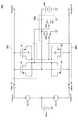
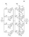
[第1の問題]
図2は、従来のMOSFETパラメトリック増幅器におけるn(negative)−MOSFEの構造を示す説明図である。なお、図2において(a)には、Track状態が示されており、(b)には、Boost状態が示されている。[First problem]
FIG. 2 is an explanatory diagram showing the structure of n (negative) -MOSFE in a conventional MOSFET parametric amplifier. In FIG. 2, (a) shows the Track state, and (b) shows the Boost state.
図2に示すように、従来のMOSFETパラメトリック増幅器においては、バイアス電圧源がスイッチSW1_1を介してn−MOSFETのGate端子に接続され、このスイッチSW1_1の接続状態(ON/OFF状態)に応じてGate端子にバイアス電圧Vbiasが印加されるようになっている。また、Source端子、およびDrain端子には、スイッチSW2_1を介して、電源電圧Vddを出力する電源(以下、「電源電圧源」という。)、または、グランドが接続されており、スイッチSW2_1の接続状態に応じてSource端子、およびDrain端子に印加される電圧が切替可能とされている。なお、Bulk端子はグランドに接続されている。 As shown in FIG. 2, in the conventional MOSFET parametric amplifier, the bias voltage source is connected to the Gate terminal of the n-MOSFET through the switch SW1_1, and Gate is set according to the connection state (ON / OFF state) of the switch SW1_1. A bias voltage Vbias is applied to the terminal. The source terminal and the drain terminal are connected to a power source (hereinafter referred to as “power source voltage source”) that outputs the power source voltage Vdd or the ground via the switch SW2_1, and the connection state of the switch SW2_1 The voltage applied to the Source terminal and the Drain terminal can be switched according to the above. The Bulk terminal is connected to the ground.
上記MOSFETパラメトリック増幅器は、Track状態において、スイッチSW1_1がON、スイッチSW2_1がグランドに接続された状態となる(図2(a))。この結果、Gate端子にバイアス電圧Vbiasが印加されるとともに、Source端子とDrain端子がグランド電圧に維持される。ここで、バイアス電圧Vbiasをn−MOSFETの閾値電圧Vtよりも高く設定した場合、n−MOSFETは強い反転状態となり、酸化膜AとP基盤(P−substrate)との界面には反転層Bが形成され、電子(Electrons)が蓄積される。この結果として、n−MOSFETの静電容量は増大する。 In the Track state, the MOSFET parametric amplifier is in a state in which the switch SW1_1 is ON and the switch SW2_1 is connected to the ground (FIG. 2A). As a result, the bias voltage Vbias is applied to the Gate terminal, and the Source terminal and the Drain terminal are maintained at the ground voltage. Here, when the bias voltage Vbias is set higher than the threshold voltage Vt of the n-MOSFET, the n-MOSFET is in a strong inversion state, and the inversion layer B is formed at the interface between the oxide film A and the P substrate (P-substrat). As a result, electrons are accumulated. As a result, the capacitance of the n-MOSFET increases.
次に、図2(b)に示すように、スイッチSW1_1がOFF、スイッチSW2_1が電源電圧源側に接続されると、Source端子とDrain端子に電源電圧Vddが印加され、かつ、バイアス電圧Vbiasは印加されていない状態に変化する。この状態においては、Source端子とDrain端子に印加された電源電圧Vddにより、図2(a)において酸化膜AとP基盤(P−substrate)との界面に生じた反転層Bが消失し、負イオン(Negative Ions)が増えてn−MOSFETの静電容量は減少する。また、このとき、Gate端子には電荷が保持されている状態にあるので、図2(b)のようにスイッチの接続状態が変化し、静電容量の変化が生じるとGate端子の電圧はバイアス電圧Vbiasを容量変化比倍にBoost(増幅)した値に変化することになる(数式1参照)。なお、図2では、n−MOSFETを示したが、p(positive)−MOSFETであっても、導電性が逆となり、また、Bulk端子が電源電圧Vddを出力する電源電圧源側に接続されるという違いはあるが、Gate端子の電圧の増幅の原理は同様となる。以下、従来のMOSFETパラメトリック増幅器の説明は、n−MOSFETを用いて行う。 Next, as shown in FIG. 2B, when the switch SW1_1 is OFF and the switch SW2_1 is connected to the power supply voltage source side, the power supply voltage Vdd is applied to the Source terminal and the drain terminal, and the bias voltage Vbias is It changes to the state where it is not applied. In this state, the inversion layer B generated at the interface between the oxide film A and the P substrate (P-substrate) in FIG. 2A disappears due to the power supply voltage Vdd applied to the source terminal and the drain terminal. As the number of ions (Negative Ions) increases, the capacitance of the n-MOSFET decreases. At this time, since the charge is held in the Gate terminal, the connection state of the switch changes as shown in FIG. 2B, and when the capacitance changes, the voltage of the Gate terminal is biased. The voltage Vbias changes to a value boosted by a capacity change ratio (see Formula 1). In FIG. 2, an n-MOSFET is shown. However, even in the case of a p (positive) -MOSFET, the conductivity is reversed, and the Bulk terminal is connected to the power supply voltage source that outputs the power supply voltage Vdd. However, the principle of amplification of the voltage at the Gate terminal is the same. Hereinafter, the conventional MOSFET parametric amplifier will be described using an n-MOSFET.
ところで、上述したように、Gate端子の電圧の変化(増幅)は、反転層Bの変化に起因して生じる。ここで、MOSFETの場合、Gate端子−Source端子間、またはGate端子−Drain端子間(図2(b)におけるC)の電位差、すなわち、Gate端子に印加される電圧の大きさに留意しつつ、素子の耐圧性を決めなければならない。このため、静電容量の変化によってGate端子の電圧がBoostされると、Gate端子の電圧を増幅したMOSFET(すなわち、実際にBoostを行っているMOSFET)の耐圧性だけではなく、当該増幅された電圧が入力される後段のMOSFETの耐圧性をも考慮しなければならなくなる。したがって、従来のMOSFETパラメトリック増幅器を備える回路では、MOSFETパラメトリック増幅器から出力される出力信号の取り扱いが難しくなる。 By the way, as described above, the change (amplification) of the voltage at the Gate terminal is caused by the change of the inversion layer B. Here, in the case of MOSFET, paying attention to the potential difference between the Gate terminal and the Source terminal or between the Gate terminal and the Drain terminal (C in FIG. 2B), that is, the magnitude of the voltage applied to the Gate terminal, The pressure resistance of the element must be determined. For this reason, when the voltage at the Gate terminal is boosted due to a change in capacitance, not only the withstand voltage of the MOSFET that amplifies the voltage at the Gate terminal (that is, the MOSFET that actually performs the boost) but also the amplified voltage. It also becomes necessary to consider the withstand voltage of the subsequent MOSFET to which the voltage is input. Therefore, in a circuit including a conventional MOSFET parametric amplifier, it becomes difficult to handle an output signal output from the MOSFET parametric amplifier.
[第2の問題]
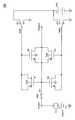
次に、上記従来のMOSFETパラメトリック増幅器における第2の問題について、図3、および図4を参照しつつ説明する。なお、図3は、上述した図2の模式図を回路図化した図であり、図3(a)に、Track状態、図3(b)に、Boost状態を各々示している。[Second problem]
Next, the second problem in the conventional MOSFET parametric amplifier will be described with reference to FIGS. FIG. 3 is a circuit diagram of the schematic diagram of FIG. 2 described above. FIG. 3A shows the Track state, and FIG. 3B shows the Boost state.
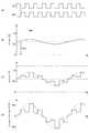
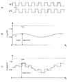
また、図4は、図3に示す従来のMOSFETパラメトリック増幅器10に係る信号の波形を示す説明図であり、図4(a)には、図3が備えるスイッチを制御する制御クロック信号、図4(b)には、従来のMOSFETパラメトリック増幅器10に入力される入力電圧信号Vinput1_1、また、図4(c)には、従来のMOSFETパラメトリック増幅器10から出力される出力電圧信号Voutput1_1を各々示している。 4 is an explanatory diagram showing waveforms of signals related to the conventional MOSFET
ここで、従来のMOSFETパラメトリック増幅器10において、以下の関係が成立する場合を想定する。
(1)スイッチSW1_1が、図4(a)に示すクロック信号φ1_1と同期して作動し、クロック信号φ1_1がハイ(high)の時「ON」、ロー(low)の時「OFF」。
(2)スイッチSw2_1が、図4(a)に示すクロック信号φ2_1と同期して作動し、クロック信号φ2_1がハイ(high)の時「電源電圧源側に接続」、ロー(low)の時「グランド側に接続」。Here, in the conventional MOSFET
(1) The switch SW1_1 operates in synchronization with the clock signal φ1_1 shown in FIG. 4A, and is “ON” when the clock signal φ1_1 is high and “OFF” when the clock signal φ1_1 is low.
(2) The switch Sw2_1 operates in synchronization with the clock signal φ2_1 shown in FIG. 4A, and is “connected to the power supply voltage source” when the clock signal φ2_1 is high, and “ Connected to ground side ".
なお、従来のMOSFETパラメトリック増幅器10に入力される入力電圧信号Vinput1_1は、図4(b)に示すように、バイアス電圧Vbiasと電圧信号Vinとが重畳された信号である。 The input voltage signal Vinput1_1 input to the conventional MOSFET
この例においては、クロック信号φ1_1が「ハイ」になっている間、スイッチSW1_1が「ON」となり、また、このとき、クロック信号φ1_1に対して反転したクロック信号φ2_1は「ロー」となりスイッチSW2_1がグランドに接続される。この結果、従来のMOSFETパラメトリック増幅器10は、Track状態(図3(a))となり、Gate酸化膜のP基盤側に反転層が形成されて、Gate端子の電圧が入力電圧信号Vinput1_1に追従して変化し、n−MOSFETに電荷が蓄積される。 In this example, while the clock signal φ1_1 is “high”, the switch SW1_1 is “ON”, and at this time, the clock signal φ2_1 inverted with respect to the clock signal φ1_1 is “low” and the switch SW2_1 is turned on. Connected to ground. As a result, the conventional MOSFET
次に、クロック信号φ1_1が「ロー」に変化すると、スイッチSW1_1が「OFF」となる。また、このとき、クロック信号φ2_1は、クロック信号φ1_1に追従して「ハイ」となり、スイッチSW2_1が電源電圧源に接続される(実際には、両信号の反転タイミングは、ずれているが、この点については後述する)。この結果、従来のMOSFETパラメトリック増幅器10は、Boost状態に遷移し、n−MOSFETの静電容量は減少する。このとき、n−MOSFETのGate端子は電荷を保持しているので、数式1に示すように静電容量の変化に応じて、入力電圧信号Vinput1_1が容量変化比倍に増幅された値となる。なお、図3では示していないが、図4(a)に示すように、クロック信号φ1_1が立ち下がってからクロック信号φ2_1が立ち上がることで(すなわち、両信号の反転タイミングに時間差があることにより)、図3(a)に示すTrack状態からHold状態を経て、図3(b)に示すBoost状態に遷移する。 Next, when the clock signal φ1_1 changes to “low”, the switch SW1_1 is turned “OFF”. At this time, the clock signal φ2_1 goes “high” following the clock signal φ1_1, and the switch SW2_1 is connected to the power supply voltage source (actually, the inversion timing of both signals is shifted, but this The point will be described later). As a result, the conventional MOSFET
ここで、この従来のMOSFETパラメトリック増幅器10がBoost状態に遷移した際の、n−MOSFETのGate端子の電圧(Boost電圧)、すなわち、MOSFETパラメトリック増幅器10の出力電圧Voutput1_1を考える。このとき、図4(c)に示すように、出力電圧Voutput1_1は、入力電圧Vinput1_1(=バイアス電圧Vbias+電圧信号Vin)が容量変化比倍(k倍)に増幅された値となる。すなわち、本来Boostすべき電圧信号Vinのみならず、バイアス電圧Vbiasもこれに伴って容量変化比倍されてしまうのである。したがって、従来のMOSFETパラメトリック増幅器10を備える回路では、出力電圧Voutput1_1が必要以上に高くなってしまい、回路の微細化や低消費電力化に適さなくなる。なお、図4(c)では、増幅された電圧信号Vinが一部k’(0<k’<k)倍の増幅となるなど、出力電圧Voutput1_1に歪みが生じているが、これについては、次述する。 Here, consider the voltage (Boost voltage) of the Gate terminal of the n-MOSFET when the conventional MOSFET
[第3の問題]
上述した従来のMOSFETパラメトリック増幅器10における第2の問題では、出力電圧Voutput1_1が必要以上に大きくなることを述べたが、図4(c)を参照すると、出力電圧Voutput1_1に上述した歪みが生じていることが分かる。そこで、次に、従来のMOSFETパラメトリック増幅器10における第3の問題として、出力電圧Voutput1_1に歪みが生じる問題を取り上げる。[Third problem]
In the second problem in the conventional MOSFET
図5は、従来のMOSFETパラメトリック増幅器10における出力電圧信号Voutputの歪みの要因を示す説明図である。図5(a)は、図4(c)の出力電圧信号Voutput1_1を連続時間波形として抜き出した周波数5MHzの波形を示す説明図である。また、図5(b)は、図5(a)の周波数スペクトラムを示す説明図である。 FIG. 5 is an explanatory diagram showing the cause of distortion of the output voltage signal Voutput in the conventional MOSFET
図5(b)を参照すると、5MHzの基本波以外に、−60[dB]のDC(direct current)成分と5MHzより周波数が大きな高調波成分が存在しており、これらのDC成分と高調波成分とが、出力電圧Voutput1_1を歪ませている。上記歪みは、出力電圧Voutput1_1が電源電圧Vddよりも大きくなった際に、n−MOSFETの静電容量が低下することに起因している。このため、図4(c)において、出力電圧Voutput1_1に生じる歪みは容量変化比が大きくなればなるほど、大きくなるという関係を有する。 Referring to FIG. 5B, in addition to the fundamental frequency of 5 MHz, a DC (direct current) component of −60 [dB] and a harmonic component having a frequency higher than 5 MHz exist, and these DC component and harmonics are present. The component distorts the output voltage Voutput1_1. The distortion is caused by a decrease in the capacitance of the n-MOSFET when the output voltage Voutput1_1 is higher than the power supply voltage Vdd. Therefore, in FIG. 4C, there is a relationship that the distortion generated in the output voltage Voutput1_1 increases as the capacitance change ratio increases.
すなわち、従来のMOSFETパラメトリック増幅器10を備える回路では、MOSFETパラメトリック増幅器から出力される出力電圧Voutput1_1のBoost時に、出力電圧Voutput1_1に歪みが生じるため、出力電圧Voutput1_1を受け取る構成要素が、適宜出力電圧Voutput1_1の補正などを行わなければならなくなってしまう。 That is, in the circuit including the conventional MOSFET
以上のように、従来のMOSFETパラメトリック増幅器10は、MOSFETパラメトリック増幅器に入力されるバイアス電圧と電圧信号とが重畳されたまま一緒に増幅されてしまうため、少なくとも上述した3つの問題を生じさせる。そこで、本実施形態に係る増幅器においては、概略、以下の手法により、上記問題を解決する手法を採用することとした。 As described above, the conventional MOSFET
(本発明に係る増幅器における増幅の原理)
まず、本発明に係る増幅器の増幅原理について図6および図7を参照しつつ説明する。なお、図6は、本発明の実施形態に係る増幅器のTrack状態とHold状態とを示す説明図であり、図6(a)は、Track状態、図6(b)は、Hold状態を夫々示している。(Principle of amplification in the amplifier according to the present invention)
First, the amplification principle of the amplifier according to the present invention will be described with reference to FIGS. 6A and 6B are explanatory diagrams showing the Track state and the Hold state of the amplifier according to the embodiment of the present invention. FIG. 6A shows the Track state, and FIG. 6B shows the Hold state. ing.
また、図7は、本発明の実施形態に係る増幅器のBoost状態における電荷の移動を示す説明図であり、図7(a)〜(c)は、各々、Boost状態における電荷の移動を経時的に示している。 FIG. 7 is an explanatory view showing the movement of charges in the boost state of the amplifier according to the embodiment of the present invention. FIGS. 7A to 7C show the movement of charges in the boost state over time. It shows.
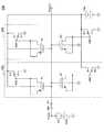
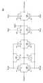
図6と図7を参照すると、本発明の実施形態に係る増幅器は、(1)静電容量が可変する第1可変静電容量素子Pと、(2)第1可変静電容量素子Pと逆導電型の第2可変静電容量素子Nとを有しており、第1可変静電容量素子Pと逆導電型の第2可変静電容量素子Nとには、スイッチSW1の接続状態に応じてバイアス電圧Vdd/2と電圧信号Vinとが入力される。また、第1可変静電容量素子Pは電源電圧源と接続され、第2可変静電容量素子Nはグランドに接続される。なお、図6と図7とでは、バイアス電圧をVdd/2としたが、上記に限られないことは、言うまでもない。 6 and 7, the amplifier according to the embodiment of the present invention includes (1) a first variable capacitance element P whose capacitance is variable, and (2) a first variable capacitance element P. The second variable capacitance element N of reverse conductivity type is included, and the switch SW1 is connected to the first variable capacitance element P and the second variable capacitance element N of reverse conductivity type. Accordingly, a bias voltage Vdd / 2 and a voltage signal Vin are input. The first variable capacitance element P is connected to a power supply voltage source, and the second variable capacitance element N is connected to the ground. In FIGS. 6 and 7, the bias voltage is Vdd / 2, but it is needless to say that the bias voltage is not limited to the above.
まず、図6(a)に示すように、スイッチSW1が「ON」状態の時、バイアス電圧Vdd/2と電圧信号VinとがスイッチSW1を通じて入力されることにより、第1可変静電容量素子Pの両端には、Vp1=Vdd/2−Vinが印加され、また、第2可変静電容量素子Nの両端には、Vn1=Vdd/2+Vinが印加される。この結果、第1可変静電容量素子Pと第2可変静電容量素子Nに電荷が蓄えられる。 First, as shown in FIG. 6A, when the switch SW1 is in the “ON” state, the bias voltage Vdd / 2 and the voltage signal Vin are input through the switch SW1, thereby the first variable capacitance element P. Vp1 = Vdd / 2−Vin is applied to both ends of Vn1, and Vn1 = Vdd / 2 + Vin is applied to both ends of the second variable capacitance element N. As a result, charges are stored in the first variable capacitance element P and the second variable capacitance element N.
この状態において、スイッチSW1が開いてバイアス電圧Vdd/2と電圧信号Vinとが入力されていない状態(Hold状態)になると、増幅器においては以下の関係が成立する。
(1)第1可変静電容量素子PのGate端子(図6(b)におけるスイッチSW1と接続される側の端子)には、スイッチSW1が開く直前の電荷Qp1=−C1・Vp1=−C1(Vdd/2−Vin)が保持される。
(2)第2可変静電容量素子NのGate端子(図6(b)におけるスイッチSW1と接続される側の端子)には、スイッチSW1が開く直前の電荷Qn1=C1・Vn1=C1(Vdd/2+Vin)が保持される。In this state, when the switch SW1 is opened and the bias voltage Vdd / 2 and the voltage signal Vin are not input (Hold state), the following relationship is established in the amplifier.
(1) The charge Qp1 = −C1 · Vp1 = −C1 immediately before the switch SW1 is opened is connected to the Gate terminal of the first variable capacitance element P (the terminal connected to the switch SW1 in FIG. 6B). (Vdd / 2−Vin) is held.
(2) The charge Qn1 = C1 · Vn1 = C1 (Vdd immediately before the switch SW1 is opened) is connected to the Gate terminal of the second variable capacitance element N (the terminal connected to the switch SW1 in FIG. 6B). / 2 + Vin) is held.
ここで、第1可変静電容量素子PのGate端子と第2可変静電容量素子NのGate端子とにおける電荷の差分は、電圧信号Vinに比例した量となる。 Here, the difference in charge between the Gate terminal of the first variable capacitance element P and the Gate terminal of the second variable capacitance element N is an amount proportional to the voltage signal Vin.
次に図7を参照してBoost状態について説明する。図7(a)は、図6(b)と同様にHold状態を示す図であるが、Boost状態における電荷の移動を説明するために、図6(b)にはないスイッチSW0を更に設けた構成として示している。ここで、スイッチSW0は、図7に示すように、第1可変静電容量素子Pと電源電圧源との接続を制御するスイッチであるが、説明の便宜上の架空のスイッチである。つまり、図6(b)と図7(a)とは、実質的に同一である。 Next, the Boost state will be described with reference to FIG. FIG. 7A is a diagram showing the Hold state as in FIG. 6B, but in order to explain the movement of charges in the Boost state, a switch SW0 not provided in FIG. 6B is further provided. Shown as a configuration. Here, as shown in FIG. 7, the switch SW0 is a switch that controls the connection between the first variable capacitance element P and the power supply voltage source, but is a fictitious switch for convenience of explanation. That is, FIG. 6B and FIG. 7A are substantially the same.
図7(a)を参照すると、スイッチSW0が開いているため、図6(b)と同様に第1可変静電容量素子PのGate端子の電荷は、Qp1=−C1・Vp1=−C1(Vdd/2−Vin)であり、また、第2可変静電容量素子NのGate端子の電荷は、Qn1=C1・Vn1=C1(Vdd/2+Vin)となる。なお、その他の状態は、図6(b)と同様である。 Referring to FIG. 7A, since the switch SW0 is open, the charge at the Gate terminal of the first variable capacitance element P is Qp1 = −C1 · Vp1 = −C1 (like FIG. 6B). Vdd / 2−Vin), and the charge at the Gate terminal of the second variable capacitance element N is Qn1 = C1 · Vn1 = C1 (Vdd / 2 + Vin). The other states are the same as in FIG.
この状態で、第1可変静電容量素子Pの静電容量と第2可変静電容量素子Nの静電容量を「1/k」倍(すなわち、変化後の静電容量C2=C1/k)に減少させた場合を想定する(図7(b))。このとき、第1可変静電容量素子PのGate端子の電荷は、Qp1=−C1・Vp1=−C1(Vdd/2−Vin)=−kC2(Vdd/2−Vin)と表すことができ、同様に、第2可変静電容量素子NのGate端子の電荷は、Qn1=C1・Vn1=C1(Vdd/2+Vin)=kC2(Vdd/2+Vin)と表すことができる。 In this state, the capacitance of the first variable capacitance element P and the capacitance of the second variable capacitance element N are multiplied by “1 / k” (that is, the changed capacitance C2 = C1 / k). ) Is assumed (FIG. 7B). At this time, the charge at the Gate terminal of the first variable capacitance element P can be expressed as Qp1 = −C1 · Vp1 = −C1 (Vdd / 2−Vin) = − kC2 (Vdd / 2−Vin), Similarly, the charge at the Gate terminal of the second variable capacitance element N can be expressed as Qn1 = C1 · Vn1 = C1 (Vdd / 2 + Vin) = kC2 (Vdd / 2 + Vin).
また、第1可変静電容量素子Pの両端にかかる電圧Vp2’は、Vp2’=k(Vdd/2−Vin)となり、容量変化比k倍に増幅される。同様に、第2可変静電容量素子Nの両端にかかる電圧Vn2’は、Vn2’=k(Vdd/2+Vin)となり、容量変化比k倍に増幅される。なお、上記電圧の増幅の原理は、上述した数式1に示す離散時間パラメトリック増幅器の原理と同様である。 Further, the voltage Vp2 'applied to both ends of the first variable capacitance element P becomes Vp2' = k (Vdd / 2-Vin), and is amplified by a capacitance change ratio k times. Similarly, the voltage Vn2 'applied to both ends of the second variable capacitance element N is Vn2' = k (Vdd / 2 + Vin), and is amplified by a capacitance change ratio k times. The principle of voltage amplification is the same as that of the discrete-time parametric amplifier shown in
次に、図7(c)に示すように、図7(b)の状態から、スイッチSW0が閉じられると、第1可変静電容量素子Pが電源電圧源に接続される。このとき、第1可変静電容量素子Pと第2可変静電容量素子Nとには、電源電圧Vddがかかり、第1可変静電容量素子Pから電源電圧源側へ電荷Q’=(k−1)C2・Vdd/2が移動する。そして、電荷Q’の移動と同時に、第1可変静電容量素子PのGate端子と第2可変静電容量素子NのGate端子とでは、電荷Q’に相当する量の電荷が消滅することとなる。すなわち、第1可変静電容量素子PのGate端子の電荷は、Qp2=−C2(Vdd/2−kVin)となり、また、第2可変静電容量素子NのGate端子の電荷は、Qn2=C2(Vdd/2+kVin)となる。 Next, as shown in FIG. 7C, when the switch SW0 is closed from the state of FIG. 7B, the first variable capacitance element P is connected to the power supply voltage source. At this time, the power supply voltage Vdd is applied to the first variable capacitance element P and the second variable capacitance element N, and the charge Q ′ = (k) from the first variable capacitance element P to the power supply voltage source side. -1) C2 · Vdd / 2 moves. Simultaneously with the movement of the charge Q ′, an amount of charge corresponding to the charge Q ′ disappears at the Gate terminal of the first variable capacitance element P and the Gate terminal of the second variable capacitance element N. Become. That is, the charge at the Gate terminal of the first variable capacitance element P is Qp2 = −C2 (Vdd / 2−kVin), and the charge at the Gate terminal of the second variable capacitance element N is Qn2 = C2. (Vdd / 2 + kVin).
ここで、第1可変静電容量素子PのGate端子と第2可変静電容量素子NのGate端子とにおける電荷の差分は保持されるため、第1可変静電容量素子Pの両端にかかる電圧Vp2は、数式2で表され、また、第2可変静電容量素子Nの両端にかかる電圧Vn2は、数式3で表される。 Here, since the difference in charge between the Gate terminal of the first variable capacitance element P and the Gate terminal of the second variable capacitance element N is maintained, the voltage applied to both ends of the first variable capacitance element P. Vp2 is expressed by
したがって、本発明の実施形態に係る増幅器は、バイアス電圧と電圧信号とが重畳されたまま一緒に増幅される従来のMOSFETパラメトリック増幅器10とは異なり、電圧信号Vinはk(容量変化比)倍に増幅されるが、バイアス電圧Vdd/2=Vbiasは増幅されない。したがって、本発明の実施形態に係る増幅器は、従来のMOSFETパラメトリック増幅器10のように必要以上に出力電圧が大きくなることはないので、上述した従来のMOSFETパラメトリック増幅器10における3つの問題が生じる可能性を非常に小さくでき、回路の微細化および低消費電力化に寄与することができる。 Therefore, the amplifier according to the embodiment of the present invention is different from the conventional MOSFET
なお、上記では、第1可変静電容量素子Pおよび第2可変静電容量素子Nについて、図6、図7におけるスイッチSW1と接続される側の端子を、それぞれ第1可変静電容量素子PのGate端子、第2可変静電容量素子NのGate端子として説明した。しかしながら、本発明に係る増幅器における増幅の原理は、上記の場合に限られず、例えば、図6、図7におけるスイッチSW1と接続される側の端子を、それぞれ第1可変静電容量素子PのSource端子およびDrain端子、第2可変静電容量素子NのSource端子およびDrain端子とした場合であっても適用することができる。 In the above description, for the first variable capacitance element P and the second variable capacitance element N, the terminals connected to the switch SW1 in FIGS. 6 and 7 are respectively connected to the first variable capacitance element P. The gate terminal of the second variable capacitance element N has been described. However, the principle of amplification in the amplifier according to the present invention is not limited to the above case. For example, the terminal connected to the switch SW1 in FIGS. 6 and 7 is connected to the source of the first variable capacitance element P, respectively. The present invention can be applied even when the terminal and the drain terminal, the source terminal and the drain terminal of the second variable capacitance element N are used.
ここで、図6、図7におけるスイッチSW1と接続される側の端子を、それぞれ第1可変静電容量素子PのSource端子およびDrain端子、第2可変静電容量素子NのSource端子およびDrain端子とする場合には、例えば、図6、図7において、第1可変静電容量素子Pと第2可変静電容量素子Nとを入れ替えればよい。本発明の実施形態に係る増幅器は、例えば、上記のような構成をとることにより、上述した従来のMOSFETパラメトリック増幅器10における3つの問題が生じる可能性を非常に小さくでき、回路の微細化および低消費電力化に寄与することができる。なお、本発明に係る増幅器が、Gate端子、Source端子、およびDrain端子を備える構成に限られないことは、言うまでもない。 Here, the terminals connected to the switch SW1 in FIGS. 6 and 7 are the source terminal and drain terminal of the first variable capacitance element P, and the source terminal and drain terminal of the second variable capacitance element N, respectively. In such a case, for example, the first variable capacitance element P and the second variable capacitance element N may be interchanged in FIGS. In the amplifier according to the embodiment of the present invention, for example, by taking the configuration as described above, the possibility of the occurrence of the three problems in the above-described conventional MOSFET
また、以下では、スイッチSW1と接続される側の端子を、それぞれ第1可変静電容量素子PのGate端子、第2可変静電容量素子NのGate端子として説明する。 Hereinafter, the terminals connected to the switch SW1 will be described as the Gate terminal of the first variable capacitance element P and the Gate terminal of the second variable capacitance element N, respectively.
(本発明に係る増幅の原理を用いた増幅方法)
以上の原理に基づく本実施形態に係る増幅方法について、図8を参照して説明する。図8は、本発明に係る増幅の原理を用いた増幅方法を示す流れ図である。(Amplification method using the principle of amplification according to the present invention)
An amplification method according to this embodiment based on the above principle will be described with reference to FIG. FIG. 8 is a flowchart showing an amplification method using the principle of amplification according to the present invention.
バイアス電圧と電圧信号とが入力され、第1可変静電容量素子と第2可変静電容量素子とに第1静電容量に対応する第1電荷を蓄積する(S100)。 The bias voltage and the voltage signal are input, and the first charge corresponding to the first capacitance is stored in the first variable capacitance device and the second variable capacitance device (S100).
上記バイアス電圧と上記電圧信号との入力を止め、ステップS100で蓄積された電荷を保持する(S102)。このとき、第1可変静電容量素子と第2可変静電容量素子とには、上記バイアス電圧と上記電圧信号とに相当する電圧がかかっている。 The input of the bias voltage and the voltage signal is stopped, and the charge accumulated in step S100 is held (S102). At this time, a voltage corresponding to the bias voltage and the voltage signal is applied to the first variable capacitance element and the second variable capacitance element.
ステップS102で保持された電荷を保持したままで、第1可変静電容量素子と第2可変静電容量素子との静電容量を、第1静電容量から、第1静電容量よりも小さな第2静電容量へと減少させる(S104)。 While holding the electric charge held in step S102, the capacitance of the first variable capacitance element and the second variable capacitance element is smaller than the first capacitance from the first capacitance. Decrease to the second capacitance (S104).
ステップS104で変化した静電容量の容量変化比(第1静電容量/第2静電容量)に応じて、第1可変静電容量素子と第2可変静電容量素子とにかかっているバイアス電圧と電圧信号とを増幅する(S106)。 Bias applied to the first variable capacitance element and the second variable capacitance element in accordance with the capacitance change ratio (first capacitance / second capacitance) changed in step S104. The voltage and the voltage signal are amplified (S106).
ステップS106において、第1可変静電容量素子と第2可変静電容量素子とで増幅されたバイアス電圧の増幅量に相当する電荷を相殺する(S108)。ここで、上記バイアス電圧の増幅量に相当する電荷の相殺は、電源電圧Vddが第1可変静電容量素子と第2可変静電容量素子とにかかることにより生じる。 In step S106, the charge corresponding to the amplification amount of the bias voltage amplified by the first variable capacitance element and the second variable capacitance element is canceled (S108). Here, charge cancellation corresponding to the amount of amplification of the bias voltage occurs when the power supply voltage Vdd is applied to the first variable capacitance element and the second variable capacitance element.
以上のステップS100〜ステップS108により、本発明に係る増幅の原理を用いた増幅方法は、増幅器に入力されるバイアス電圧と電圧信号とのうち、当該電圧信号を増幅する。 Through the above steps S100 to S108, the amplification method using the principle of amplification according to the present invention amplifies the voltage signal out of the bias voltage and the voltage signal input to the amplifier.
なお、ステップS104では、第1可変静電容量素子と第2可変静電容量素子との静電容量を、第1静電容量から、第1静電容量よりも小さな第2静電容量へと減少させたが、上記に限られず、第1可変静電容量素子と第2可変静電容量素子との静電容量を、第1静電容量から、第1静電容量よりも大きな第3静電容量へと増加させてもよい。この場合、ステップS106では、第1可変静電容量素子と第2可変静電容量素子とにかかっているバイアス電圧と電圧信号とが減衰することとなる。 In step S104, the capacitance of the first variable capacitance element and the second variable capacitance element is changed from the first capacitance to a second capacitance smaller than the first capacitance. Although not limited to the above, the capacitance of the first variable capacitance element and the second variable capacitance element is changed from the first capacitance to the third static capacitance larger than the first capacitance. You may increase it to electric capacity. In this case, in step S106, the bias voltage and the voltage signal applied to the first variable capacitance element and the second variable capacitance element are attenuated.
(第1の実施形態)
次に、上述した本発明に係る増幅の原理を用いた、本発明に係る増幅器の実施形態について図9および図10を参照しつつ説明する。図9は、本発明の第1の実施形態に係る増幅器100を示す説明図であり、(a)には、増幅器100のTrack状態を、(b)には、増幅器100のBoost状態を示している。(First embodiment)
Next, an embodiment of an amplifier according to the present invention using the above-described principle of amplification according to the present invention will be described with reference to FIGS. FIG. 9 is an explanatory diagram showing the
また、図10(a)は、図9が備えるスイッチを制御する制御クロック信号を示す図であり、図10(b)は、本発明の第1の実施形態に係る増幅器100に入力される入力電圧信号Vinputを示す図であり、図10(c)は、本発明の第1の実施形態に係る増幅器100から出力される出力電圧信号Voutputを示す図である。 FIG. 10A is a diagram illustrating a control clock signal for controlling the switch included in FIG. 9, and FIG. 10B is an input input to the
図9を参照すると、本発明の第1の実施形態に係る増幅器100は、p−MOSバラクタP1と、n−MOSバラクタN1とを有するCMOSで構成される。ここで、p−MOSバラクタP1と、n−MOSバラクタN1とは、図2に示すMOSFETと同様に、反転層の有無によって静電容量を変化させる。 Referring to FIG. 9, the
p−MOSバラクタP1とn−MOSバラクタN1とのGate端子には、スイッチSW1の接続状態に応じてバイアス電圧Vbiasと電圧信号Vinとが入力される。また、p−MOSバラクタP1のSource端子とDrain端子とは、スイッチSW2の接続状態に応じて、電源電圧源とグランドとに接続され、n−MOSバラクタN1のSource端子とDrain端子とは、スイッチSW3の接続状態に応じて、電源電圧源とグランドとに接続される。ここで、p−MOSバラクタP1と、n−MOSバラクタN1とは逆導電性を有するので、p−MOSバラクタP1とn−MOSバラクタN1との静電容量の増減変化を合わせるために、スイッチSW2が電源電圧源に接続されている場合は、スイッチSW3はグランドに接続され、また、スイッチSW2がグランドに接続されている場合は、スイッチSW3は電源電圧源に接続される。 A bias voltage Vbias and a voltage signal Vin are input to the Gate terminals of the p-MOS varactor P1 and the n-MOS varactor N1 according to the connection state of the switch SW1. The source terminal and the drain terminal of the p-MOS varactor P1 are connected to the power supply voltage source and the ground according to the connection state of the switch SW2, and the source terminal and the drain terminal of the n-MOS varactor N1 are connected to the switch. Depending on the connection state of SW3, the power supply voltage source and the ground are connected. Here, since the p-MOS varactor P1 and the n-MOS varactor N1 have reverse conductivity, the switch SW2 is used in order to match the increase and decrease in the capacitance between the p-MOS varactor P1 and the n-MOS varactor N1. Is connected to the power supply voltage source, the switch SW3 is connected to the ground, and when the switch SW2 is connected to the ground, the switch SW3 is connected to the power supply voltage source.
ここで、スイッチSW1は、図10(a)に示すクロック信号φ1と同期してクロック信号φ1がハイのとき閉じ、p−MOSバラクタP1とn−MOSバラクタN1とのGate端子に、バイアス電圧Vbiasと電圧信号Vinとを入力する。また、スイッチSW1は、クロック信号φ1がローのときに開くことにより、p−MOSバラクタP1とn−MOSバラクタN1とのGate端子とに対するバイアス電圧Vbiasと電圧信号Vinとの入力を制御する。なお、クロック信号φ1とスイッチSW1との関係は上記に限られず、例えば、クロック信号φ1がローのときスイッチSW1が閉じるとしてもよい。また、以下、本発明に係る種々の実施形態について説明するが、クロック信号とスイッチとの関係は、上記クロック信号φ1とスイッチSW1との関係と同様に、限定されるものではない。 Here, the switch SW1 is closed when the clock signal φ1 is high in synchronization with the clock signal φ1 shown in FIG. 10A, and the bias voltage Vbias is applied to the Gate terminals of the p-MOS varactor P1 and the n-MOS varactor N1. And a voltage signal Vin. The switch SW1 opens when the clock signal φ1 is low, thereby controlling the input of the bias voltage Vbias and the voltage signal Vin to the Gate terminals of the p-MOS varactor P1 and the n-MOS varactor N1. The relationship between the clock signal φ1 and the switch SW1 is not limited to the above. For example, the switch SW1 may be closed when the clock signal φ1 is low. Hereinafter, various embodiments according to the present invention will be described. However, the relationship between the clock signal and the switch is not limited in the same manner as the relationship between the clock signal φ1 and the switch SW1.
スイッチSW2は、図10(a)に示すクロック信号φ2と同期してクロック信号φ2がハイのときグランドに接続され、クロック信号φ2がローのとき電源電圧源に接続される。また、スイッチSW3は、クロック信号φ2と同期してクロック信号φ2がハイのとき電源電圧源に接続され、クロック信号φ2がローのときグランドに接続される。ここで、図10(a)に示すように、クロック信号φ1とクロック信号φ2とは、位相が重ならないように入力される。クロック信号φ1とクロック信号φ2との位相関係を重ならないようにすることにより、本発明の第1の実施形態に係る増幅器100では、Track状態、Hold状態、およびBoost状態が作り出される。 The switch SW2 is connected to the ground when the clock signal φ2 is high in synchronization with the clock signal φ2 shown in FIG. 10A, and is connected to the power supply voltage source when the clock signal φ2 is low. The switch SW3 is connected to the power supply voltage source in synchronization with the clock signal φ2 when the clock signal φ2 is high, and is connected to the ground when the clock signal φ2 is low. Here, as shown in FIG. 10A, the clock signal φ1 and the clock signal φ2 are input so that the phases do not overlap. By preventing the phase relationship between the clock signal φ1 and the clock signal φ2 from overlapping, the
また、本発明の第1の実施形態に係る増幅器100に入力される入力電圧信号Vinputは、図10(b)に示すように、バイアス電圧Vbiasと電圧信号Vinとが重畳された信号である。 Further, the input voltage signal Vinput inputted to the
図9(a)を参照すると、Track状態では、スイッチSW1がクロック信号φ1に同期して閉じることにより、p−MOSバラクタP1とn−MOSバラクタN1とのGate端子に入力電圧信号Vinputが入力される。また、スイッチSW2がクロック信号φ2に同期して電源電圧源に接続され、スイッチSW3がクロック信号φ2に同期してグランドに接続されることにより、p−MOSバラクタP1とn−MOSバラクタN1との静電容量は増加する。したがって、p−MOSバラクタP1とn−MOSバラクタN1とのGate端子の電圧は、入力電圧信号Vinputに追従して変化し、入力電圧信号Vinputに応じた電荷がp−MOSバラクタP1とn−MOSバラクタN1とに蓄積される。 Referring to FIG. 9A, in the Track state, the switch SW1 is closed in synchronization with the clock signal φ1, so that the input voltage signal Vinput is input to the Gate terminals of the p-MOS varactor P1 and the n-MOS varactor N1. The Further, the switch SW2 is connected to the power supply voltage source in synchronization with the clock signal φ2, and the switch SW3 is connected to the ground in synchronization with the clock signal φ2, so that the p-MOS varactor P1 and the n-MOS varactor N1 are connected. The capacitance increases. Therefore, the voltage at the Gate terminal of the p-MOS varactor P1 and the n-MOS varactor N1 changes following the input voltage signal Vinput, and the charge corresponding to the input voltage signal Vinput changes between the p-MOS varactor P1 and the n-MOS. Accumulated in the varactor N1.
次に図9(b)を参照すると、Boost状態では、スイッチSW1がクロック信号φ1に同期して開くことにより、p−MOSバラクタP1とn−MOSバラクタN1とのGate端子に入力電圧信号Vinputは入力されず、また、スイッチSW2がクロック信号φ2に同期してグランドに接続され、スイッチSW3がクロック信号φ2に同期して電源電圧源に接続されることにより、p−MOSバラクタP1とn−MOSバラクタN1との静電容量は減少する。このとき、p−MOSバラクタP1とn−MOSバラクタN1とのGate端子は電荷を保持しているので、数式2、3に示すように静電容量の変化によって、バイアス電圧Vbiasの大きさが保持されたまま、電圧信号Vinが容量変化比倍に増幅される。したがって、本発明の第1の実施形態に係る増幅器100の出力電圧Voutputは、図10(c)に示すように、入力電圧信号Vinputに対して、バイアス電圧Vbiasの大きさが保持されたまま、電圧信号Vinが容量変化比倍に増幅された波形となる。ここで、出力電圧Voutputは、電源電圧Vddよりも小さいため、従来のMOSFETパラメトリック増幅器10のように出力電圧に歪みは生じていない。なお、図9では示していないが、図10(a)に示すように、クロック信号φ1が立ち下がってからクロック信号φ2が立ち上がることで、図9(a)に示すTrack状態からHold状態を経て、図9(b)に示すBoost状態に遷移する。 Next, referring to FIG. 9B, in the Boost state, the switch SW1 is opened in synchronization with the clock signal φ1, so that the input voltage signal Vinput is applied to the Gate terminals of the p-MOS varactor P1 and the n-MOS varactor N1. Since the switch SW2 is connected to the ground in synchronization with the clock signal φ2 and the switch SW3 is connected to the power supply voltage source in synchronization with the clock signal φ2, the p-MOS varactor P1 and the n-MOS are not input. The capacitance with the varactor N1 decreases. At this time, since the gate terminals of the p-MOS varactor P1 and the n-MOS varactor N1 hold charges, the magnitude of the bias voltage Vbias is held by the change in capacitance as shown in
したがって、本発明の第1の実施形態に係る増幅器100は、入力電圧信号に対して、バイアス電圧の大きさが保持されたまま、電圧信号が容量変化比倍に増幅された出力電圧信号を出力することができるので、出力電圧信号が必要以上に大きくなることはない。したがって、本発明の第1の実施形態に係る増幅器を備える回路では、本発明の第1の実施形態に係る増幅器の出力電圧信号に対して特別な対策を講じる必要はなくなるため、当該出力電圧信号の取り扱いが容易となり、また、回路の微細化および低消費電力化に寄与することができる。さらには、出力電圧信号の大きさが、電源電圧Vddよりも大きくなる可能性を非常に低くすることができるので、出力電圧信号に歪みが生じず、所望の出力電圧信号を得ることができる。 Therefore, the
[第1の実施形態の変形例]
図9に示す本発明の第1の実施形態に係る増幅器100では、p−MOSバラクタP1およびn−MOSバラクタN1のGate端子がスイッチSW1に接続され、p−MOSバラクタP1のSource端子およびDrain端子それぞれがスイッチSW2、そして、n−MOSバラクタN1のSource端子およびDrain端子それぞれがスイッチSW3に接続される構成を示した。しかしながら、本発明の第1の実施形態に係る増幅器の構成は、上記に限られない。例えば、本発明の第1の実施形態に係る増幅器は、p−MOSバラクタP1のSource端子およびDrain端子と、n−MOSバラクタN1のSource端子およびDrain端子とが、それぞれスイッチSW1に接続され、n−MOSバラクタN1のGate端子がスイッチSW2、p−MOSバラクタP1のGate端子がスイッチSW3に接続させることもできる。[Modification of First Embodiment]
In the
ここで、p−MOSバラクタP1と、n−MOSバラクタN1とはそれぞれ逆導電性を有する。このため、静電容量の増減変化を合わせるために、増幅器100と同様に、
(1)スイッチSW2が電源電圧源に接続されている場合は、スイッチSW3はグランドに接続され、また、
(2)スイッチSW2がグランドに接続されている場合は、スイッチSW3は電源電圧源に接続される。Here, the p-MOS varactor P1 and the n-MOS varactor N1 have reverse conductivity. For this reason, in order to match the increase / decrease change of the capacitance, like the
(1) When the switch SW2 is connected to the power supply voltage source, the switch SW3 is connected to the ground, and
(2) When the switch SW2 is connected to the ground, the switch SW3 is connected to the power supply voltage source.
上記の構成においても、増幅器100と同様のTrack状態、Hold状態、およびBoost状態を作り出すことができるので、数式2、3に示すように静電容量の変化によって、バイアス電圧Vbiasの大きさが保持されたまま、電圧信号Vinを容量変化比倍に増幅することができる。 Even in the above configuration, the Track state, the Hold state, and the Boost state similar to those of the
このように、本発明の第1の実施形態に係る上記増幅器は、入力電圧信号に対して、バイアス電圧の大きさが保持されたまま、電圧信号が容量変化比倍に増幅された出力電圧信号を出力することができるので、出力電圧信号が必要以上に大きくなることはない。したがって、本発明の第1の実施形態に係る上記増幅器を備える回路では、本発明の第1の実施形態に係る増幅器100を備える回路と同様に、増幅器の出力電圧信号に対して特別な対策を講じる必要はなくなるため、当該出力電圧信号の取り扱いが容易となり、また、回路の微細化および低消費電力化に寄与することができる。さらには、出力電圧信号の大きさが、電源電圧Vddよりも大きくなる可能性を非常に低くすることができるので、出力電圧信号に歪みが生じず、所望の出力電圧信号を得ることができる。 As described above, the amplifier according to the first embodiment of the present invention provides an output voltage signal obtained by amplifying the voltage signal by the capacitance change ratio while maintaining the magnitude of the bias voltage with respect to the input voltage signal. Therefore, the output voltage signal does not increase more than necessary. Therefore, in the circuit including the amplifier according to the first embodiment of the present invention, as in the circuit including the
(第2の実施形態)
本発明の実施形態に係る増幅器における増幅の原理で述べたように、本発明の実施形態に係る増幅器は、第1可変静電容量素子PのGate端子と第2可変静電容量素子NのGate端子とにおいて、同じ量の電荷を消滅させることにより、バイアス電圧の大きさを保持したまま、電圧信号を容量変化比倍に増幅する。したがって、第1可変静電容量素子PのGate端子の面積と第2可変静電容量素子NのGate端子の面積とが同一であることが望ましい。しかしながら、実際の製造工程においては、各素子の製造のばらつきなどにより、第1可変静電容量素子PのGate端子の面積と第2可変静電容量素子NのGate端子の面積とが一致しない場合もある。そこで次に、第1可変静電容量素子PのGate端子の面積と第2可変静電容量素子NのGate端子の面積との面積比を調整することが可能な第2の実施形態について説明する。図11は、本発明の第2の実施形態に係る増幅器200を示す説明図である。(Second Embodiment)
As described in the principle of amplification in the amplifier according to the embodiment of the present invention, the amplifier according to the embodiment of the present invention includes the Gate terminal of the first variable capacitance element P and the Gate of the second variable capacitance element N. By eliminating the same amount of charge at the terminal, the voltage signal is amplified to a capacitance change ratio while maintaining the magnitude of the bias voltage. Therefore, it is desirable that the area of the Gate terminal of the first variable capacitance element P and the area of the Gate terminal of the second variable capacitance element N are the same. However, in the actual manufacturing process, the area of the Gate terminal of the first variable capacitance element P and the area of the Gate terminal of the second variable capacitance element N do not match due to manufacturing variation of each element. There is also. Next, a second embodiment in which the area ratio between the area of the Gate terminal of the first variable capacitance element P and the area of the Gate terminal of the second variable capacitance element N can be adjusted will be described. . FIG. 11 is an explanatory diagram showing an
図11に示されるように、本発明の第2の実施形態に係る増幅器200は、第1の実施形態に係る増幅器100と基本的な構成は同一となっており、さらに、極小のゲート幅を有する複数の調整用p−MOSバラクタP’1〜P’4が、p−MOSバラクタP1に対して並列に設けられている。p−MOSバラクタP1のゲート幅はW=αであり、n−MOSバラクタN1のゲート幅はW=βである。また、調整用p−MOSバラクタP’1のゲート幅はW=4[μm]、同様に、調整用p−MOSバラクタP’2〜P’4のゲート幅は、それぞれW=8[μm]、16[μm]、32[μm]である。ここで、説明の便宜上、p−MOSバラクタP1、n−MOSバラクタN1、および調整用p−MOSバラクタP’1〜P’4のゲート長が1[μm]であると仮定する。 As shown in FIG. 11, an
また、調整用p−MOSバラクタP’1〜P’4のGate端子は、スイッチSW1と接続され、スイッチSW1の接続状態に応じてバイアス電圧Vbiasと電圧信号Vinとが入力される。さらに、各バラクタP’1〜P’4の接続状態は以下の関係を有している。
(1)調整用p−MOSバラクタP’1のSource端子とDrain端子とは、スイッチSW’1の接続状態に応じて、電源電圧源とグランドとに接続され、同様に、
(2)調整用p−MOSバラクタP’2〜P’4のSource端子とDrain端子とは、それぞれスイッチSW’2〜SW’4の接続状態に応じて、電源電圧源とグランドとに接続される。The gate terminals of the adjustment p-MOS varactors P′1 to P′4 are connected to the switch SW1, and the bias voltage Vbias and the voltage signal Vin are input according to the connection state of the switch SW1. Furthermore, the connection states of the varactors P′1 to P′4 have the following relationship.
(1) The Source terminal and the Drain terminal of the adjustment p-MOS varactor P′1 are connected to the power supply voltage source and the ground according to the connection state of the switch SW′1.
(2) The Source and Drain terminals of the adjustment p-MOS varactors P′2 to P′4 are connected to the power supply voltage source and the ground according to the connection state of the switches SW′2 to SW′4, respectively. The
スイッチSW’1〜SW’4をそれぞれ、p−MOSバラクタP1と同一の極性、すなわちスイッチSW2と接続先を同一にした場合、p−MOSバラクタP1のGate端子の面積は大きくなる。例えば、図11に示すように、スイッチSW2とスイッチSW’1〜SW’4とを電源電圧源に接続した場合、p−MOSバラクタP1のGate端子の面積Spは、Sp=αからSp’=α+(4+8+16+32)=α+60[μm2]となり、最大となる。また、スイッチSW2とスイッチSW’1〜SW’3とを電源電圧源に接続し、スイッチSW’4をグランドに接続した場合、p−MOSバラクタP1のGate端子の面積Spは、Sp’=α+(4+8+16)=α+28[μm2]となる。上記のように、本発明の第2の実施形態に係る増幅器200は、スイッチSW’1〜SW’4の接続をそれぞれ独立に適宜切り替えることにより、p−MOSバラクタP1のGate端子の面積Spを間接的に変化させることができる。したがって、第1可変静電容量素子PのGate端子の面積Spと第2可変静電容量素子NのGate端子の面積Sn=βとの面積比Sn/Spの値を正確に、あるいは近似的に1に調整することができる。When the switches SW′1 to SW′4 have the same polarity as that of the p-MOS varactor P1, that is, the same connection destination as that of the switch SW2, the area of the Gate terminal of the p-MOS varactor P1 increases. For example, as shown in FIG. 11, when the switch SW2 and the switches SW′1 to SW′4 are connected to the power supply voltage source, the area Sp of the Gate terminal of the p-MOS varactor P1 is changed from Sp = α to Sp ′ = α + (4 + 8 + 16 + 32) = α + 60 [μm2 ], which is the maximum. When the switch SW2 and the switches SW′1 to SW′3 are connected to the power supply voltage source and the switch SW′4 is connected to the ground, the area Sp of the Gate terminal of the p-MOS varactor P1 is Sp ′ = α + (4 + 8 + 16) = α + 28 [μm2 ]. As described above, the
ここで、図11において、調整用p−MOSバラクタP’1〜P’4のゲート幅は、2のべき乗の重み付けがなされているが、その理由は、第1可変静電容量素子PのGate端子の面積Spをbit制御するためである。例えば、図11の構成を採用した場合、4bitの制御、すなわち、第1可変静電容量素子PのGate端子の面積Wpは、16通りに変化させることが可能である。なお、第1可変静電容量素子PのGate端子の面積Wpの制御は、上記に限られず、調整用p−MOSバラクタP’1〜P’4のゲート幅を任意に設定できることは、言うまでもない。 Here, in FIG. 11, the gate widths of the adjustment p-MOS varactors P′1 to P′4 are weighted to the power of 2. The reason is that the gate of the first variable capacitance element P is gated. This is because the area Sp of the terminal is bit-controlled. For example, when the configuration of FIG. 11 is adopted, 4-bit control, that is, the area Wp of the Gate terminal of the first variable capacitance element P can be changed in 16 ways. The control of the area Wp of the Gate terminal of the first variable capacitance element P is not limited to the above, and it goes without saying that the gate widths of the adjustment p-MOS varactors P′1 to P′4 can be arbitrarily set. .
また、図11では、調整用p−MOSバラクタP’1〜P’4のGate端子を接続した状態で、調整用p−MOSバラクタP’1〜P’4のSource端子とDrain端子とに印加する電圧の極性を変化させることにより、第1可変静電容量素子PのGate端子の面積Spを間接的に変化させた。しかし、調整用p−MOSバラクタP’1〜P’4のGate端子側にスイッチを設けることにより、第1可変静電容量素子PのGate端子の面積Spを間接的に変化させることも可能である。 Further, in FIG. 11, the gate terminals of the adjustment p-MOS varactors P′1 to P′4 are connected to the source terminal and the drain terminal of the adjustment p-MOS varactors P′1 to P′4. The area Sp of the Gate terminal of the first variable capacitance element P was indirectly changed by changing the polarity of the voltage to be applied. However, it is also possible to indirectly change the area Sp of the Gate terminal of the first variable capacitance element P by providing a switch on the Gate terminal side of the adjustment p-MOS varactors P′1 to P′4. is there.
したがって、本発明の第2の実施形態に係る増幅器200は、第1可変静電容量素子PのGate端子の面積と第2可変静電容量素子NのGate端子の面積との面積比を調整することが可能となる。このため、第1可変静電容量素子PのGate端子の面積と第2可変静電容量素子NのGate端子の面積とが、例えば、素子のばらつきにより異なっている場合でも、入力電圧信号に含まれるバイアス電圧の大きさを維持することができる。 Therefore, the
また、本発明の第2の実施形態に係る増幅器200は、本発明の第1の実施形態に係る増幅器100と同様に、入力電圧信号に対して、バイアス電圧の大きさが保持されたまま、電圧信号が容量変化比倍に増幅された出力電圧信号を出力することができるので、出力電圧信号が必要以上に大きくなることはない。したがって、本発明の第2の実施形態に係る増幅器200を備える回路では、本発明の第2の実施形態に係る増幅器200の出力電圧信号に対して特別な対策を講じる必要はなくなるため、当該出力電圧信号の取り扱いが容易となり、また、回路の微細化および低消費電力化に寄与することができる。さらには、出力電圧信号の大きさが、電源電圧Vddよりも大きくなる可能性を非常に低くすることができるので、出力電圧信号に歪みが生じず、所望の出力電圧信号を得ることができる。 In addition, the
なお、図11では、第1可変静電容量素子PのGate端子の面積を調整する構成を示したが、上記に限られず、例えば、第2可変静電容量素子NのGate端子の面積を調整する、ゲート幅が極小である複数の調整用n−MOSバラクタを備えてもよいし、第1可変静電容量素子PのGate端子の面積と第2可変静電容量素子NのGate端子の面積との双方を調整する構成をとることもできる。 FIG. 11 shows the configuration for adjusting the area of the Gate terminal of the first variable capacitance element P. However, the configuration is not limited to the above. For example, the area of the Gate terminal of the second variable capacitance element N is adjusted. A plurality of adjustment n-MOS varactors having a minimum gate width, an area of the Gate terminal of the first variable capacitance element P, and an area of the Gate terminal of the second variable capacitance element N. It is also possible to take a configuration that adjusts both.
(第3の実施形態)
次に、本発明の第3の実施形態として、本発明に係る増幅の原理を用いた差動増幅回路について説明する。図12は、本発明の第3の実施形態に係る増幅器300を示す説明図である。(Third embodiment)
Next, a differential amplifier circuit using the principle of amplification according to the present invention will be described as a third embodiment of the present invention. FIG. 12 is an explanatory diagram showing an
また、図13は、図12に示す本発明の第3の実施形態に係る信号の波形を示す説明図である。ここで、図13(a)は、図12が備えるスイッチを制御する制御クロック信号を示す図であり、図13(b)は、本発明の第3の実施形態に係る増幅器300に入力される正相入力電圧信号Vinput1を示す図である。また、図13(c)は、本発明の第3の実施形態に係る増幅器300から出力される正相出力電圧信号Voutput1を示す図であり、図13(d)は、本発明の第3の実施形態に係る増幅器300から出力される差動出力電圧信号Voutput1−Voutput1Xを示す図である。ここで、差動出力電圧信号Voutput1−Voutput1XにおけるVoutput1Xは、正相出力電圧信号Voutput1と位相が反転した逆相出力電圧信号である。 FIG. 13 is an explanatory diagram showing a waveform of a signal according to the third embodiment of the present invention shown in FIG. Here, FIG. 13A is a diagram illustrating a control clock signal for controlling the switch included in FIG. 12, and FIG. 13B is input to the
図12を参照すると、本発明の第3の実施形態に係る増幅器300は、スイッチSW1の接続状態に応じてバイアス電圧Vbiasと正相電圧信号Vin/2とが重畳された正相入力電圧信号Vinput1が入力される第1増幅部302と、スイッチSW1Xの接続状態に応じてバイアス電圧Vbiasと逆相電圧信号−Vin/2とが重畳された逆相入力電圧信号Vinput1Xが入力される第2増幅部304と、第1増幅部302と第2増幅部304とを電源電圧源、またはグランドに接続するスイッチング部306とを備える。ここで、逆相入力電圧信号Vinput1Xとは、正相入力電圧信号Vinput1から位相が反転した信号である。 Referring to FIG. 12, an
第1増幅部302と第2増幅部304とは、上述した本発明の第1の実施形態に係る増幅器100と同一の構成である。第1増幅部はp−MOSバラクタP1とn−MOSバラクタN1とを備え、p−MOSバラクタP1とn−MOSバラクタN1とのGate端子には、スイッチSW1の接続状態に応じて正相入力電圧信号Vinput1が入力される。また、第2増幅部はp−MOSバラクタP2とn−MOSバラクタN2とを備え、p−MOSバラクタP2とn−MOSバラクタN2とのGate端子には、スイッチSW1Xの接続状態に応じて逆相入力電圧信号Vinput1Xが入力される。 The
スイッチング部306は、スイッチSW2、SW3を備え、スイッチSW2は、n−MOSバラクタN1とn−MOSバラクタN2とを電源電圧源、またはグランドに接続し、スイッチSW3は、p−MOSバラクタP1とp−MOSバラクタP2とを電源電圧源、またはグランドに接続する。ここで、p−MOSバラクタP1、P2と、n−MOSバラクタN1、N2とは逆導電性を有するので、p−MOSバラクタP1、P2とn−MOSバラクタN1、N2との静電容量の増減変化を合わせるために、スイッチSW2がグランドに接続されている場合は、スイッチSW3は電源電圧源に接続され、また、スイッチSW2が電源電圧源に接続されている場合は、スイッチSW3はグランドに接続される。 The
ここで、スイッチSW1は、図13(a)に示すクロック信号φ1と同期してクロック信号φ1がハイのとき閉じ、p−MOSバラクタP1とn−MOSバラクタN1とのGate端子に、図13(b)に示す正相入力電圧信号Vinput1を入力する。また、スイッチSW1は、クロック信号φ1がローのときに開くことにより、p−MOSバラクタP1とn−MOSバラクタN1とのGate端子とに対する正相入力電圧信号Vinput1の入力を制御する。 Here, the switch SW1 is closed when the clock signal φ1 is high in synchronization with the clock signal φ1 shown in FIG. 13A, and the switch SW1 is connected to the Gate terminals of the p-MOS varactor P1 and the n-MOS varactor N1 as shown in FIG. The positive phase input voltage signal Vinput1 shown in b) is input. The switch SW1 opens when the clock signal φ1 is low, thereby controlling the input of the positive phase input voltage signal Vinput1 to the gate terminals of the p-MOS varactor P1 and the n-MOS varactor N1.
また、スイッチSW1Xは、図13(a)に示すクロック信号φ1と同期してクロック信号φ1がハイのとき閉じ、p−MOSバラクタP2とn−MOSバラクタN2とのGate端子に、逆相入力電圧信号Vinput1Xを入力する。また、スイッチSW1Xは、クロック信号φ1がローのときに開くことにより、p−MOSバラクタP2とn−MOSバラクタN2とのGate端子とに対する逆相入力電圧信号Vinput1Xの入力を制御する。 The switch SW1X is closed when the clock signal φ1 is high in synchronization with the clock signal φ1 shown in FIG. 13A, and the negative phase input voltage is applied to the Gate terminals of the p-MOS varactor P2 and the n-MOS varactor N2. The signal Vinput1X is input. Further, the switch SW1X opens when the clock signal φ1 is low, thereby controlling the input of the negative phase input voltage signal Vinput1X to the Gate terminals of the p-MOS varactor P2 and the n-MOS varactor N2.
また、スイッチSW2は、図13(a)に示すクロック信号φ2と同期してクロック信号φ2がローのとき、n−MOSバラクタN1、N2をグランドに接続し、また、クロック信号φ2がハイのとき、n−MOSバラクタN1、N2を電源電圧源に接続する。SW3は、図13(a)に示すクロック信号φ2と同期してクロック信号φ2がローのとき、p−MOSバラクタP1、P2を電源電圧源に接続し、また、クロック信号φ2がハイのとき、p−MOSバラクタP1、P2をグランドに接続する。 The switch SW2 connects the n-MOS varactors N1 and N2 to the ground when the clock signal φ2 is low in synchronization with the clock signal φ2 shown in FIG. 13A, and when the clock signal φ2 is high. , N-MOS varactors N1 and N2 are connected to a power supply voltage source. SW3 connects the p-MOS varactors P1 and P2 to the power supply voltage source when the clock signal φ2 is low in synchronization with the clock signal φ2 shown in FIG. 13A, and when the clock signal φ2 is high, The p-MOS varactors P1 and P2 are connected to the ground.
第1増幅部302は、上述した本発明の第1の実施形態に係る増幅器100と同様に、図13(a)に示すクロック信号φ1、φ2に基づいて、Track状態、Hold状態、Boost状態を経ることにより、バイアス電圧Vbiasが維持されて正相電圧信号Vin/2が容量変化比倍に増幅された、図13(c)に示す正相出力電圧信号Voutput1が出力される。 Similar to the
同様に、第2増幅部304は、図13(a)に示すクロック信号φ1、φ2に基づいて、Track状態、Hold状態、Boost状態を経ることにより、バイアス電圧Vbiasが維持されて逆相電圧信号−Vin/2が容量変化比倍に増幅された逆相出力電圧信号Voutput1Xが出力される。 Similarly, the
ここで、正相出力電圧信号Voutput1と逆相出力電圧信号Voutput1Xとは、図13(d)に示す差動出力電圧信号Voutput1−Voutput1Xとして用いられる。 Here, the positive-phase output voltage signal Voutput1 and the negative-phase output voltage signal Voutput1X are used as the differential output voltage signals Voutput1-Voutput1X shown in FIG.
したがって、本発明の第3の実施形態に係る増幅器300を備える回路は、本発明の第3の実施形態に係る増幅器300から出力される正相出力電圧信号Voutput1と逆相出力電圧信号Voutput1Xとを、図13(d)に示す差動出力電圧信号Voutput1−Voutput1Xとして捉えることにより、正相出力電圧信号Voutput1と逆相出力電圧信号Voutput1Xに生じる同じ量のノイズ(偶数時歪み)を相殺することができる。 Therefore, the circuit including the
また、本発明の第3の実施形態に係る増幅器300は、正相入力電圧信号に対して、バイアス電圧の大きさが保持されたまま、正相電圧信号が容量変化比倍に増幅された正相出力電圧信号を出力することができるので、正相出力電圧信号が必要以上に大きくなることはない。同様に、逆相入力信号に対して、バイアス電圧の大きさが保持されたまま、逆相電圧信号が容量変化比倍に増幅された逆相出力電圧信号を出力することができるので、逆相出力電圧信号が必要以上に大きくなることもない。したがって、本発明の第3の実施形態に係る増幅器300を備える回路では、本発明の第3の実施形態に係る増幅器300の差動出力電圧信号に対して特別な対策を講じる必要はなくなるため、当該差動出力電圧信号の取り扱いが容易となり、また、回路の微細化および低消費電力化に寄与することができる。さらには、差動出力電圧信号の大きさが、電源電圧Vddよりも大きくなる可能性を非常に低くすることができるので、差動出力電圧信号に歪みが生じず、所望の差動出力電圧信号を得ることができる。 In addition, the
(第4の実施形態)
図14は、本発明の第4の実施形態に係る増幅器400を示す説明図である。(Fourth embodiment)
FIG. 14 is an explanatory diagram showing an
図14を参照すると、本発明の第4の実施形態に係る増幅器400は、本発明の第3の実施形態に係る増幅器300と基本的に同じ構成をとっており、差動増幅回路を構成する。また、本発明の第4の実施形態に係る増幅器400は、図12に示す本発明の第3の実施形態に係る増幅器300と比較すると、p−MOSバラクタP1とp−MOSバラクタP2とのDrain端子は互いに接続されているが、上記p−MOSバラクタそれぞれのDrain端子と、p−MOSバラクタP1とp−MOSバラクタP2とのそれぞれのSource端子とは接続されていない。また、n−MOSバラクタN1とn−MOSバラクタN2とのDrain端子は互いに接続されているが、上記n−MOSバラクタそれぞれのDrain端子と、n−MOSバラクタN1とn−MOSバラクタN2とのそれぞれのSource端子とは接続されていない。上記のような構成においても、Source端子、またはDrain端子に一方に電源電圧Vddを印加することにより、反転層を変化させて、p−MOSバラクタP1、p−MOSバラクタP2、n−MOSバラクタN1とn−MOSバラクタN2の静電容量を可変とすることができる。 Referring to FIG. 14, an
したがって、本発明の第4の実施形態に係る増幅器400は、本発明の第3の実施形態に係る増幅器300よりも配線を簡略化することができ、また、図14に示すようにスイッチSW2、SW3は、p−MOSバラクタP1、P2とn−MOSバラクタN1、N2とのSource端子としか接続されないために、スイッチSW2、SW3にかかる負荷を軽減することができる。 Therefore, the
また、本発明の第4の実施形態に係る増幅器400は、本発明の第3の実施形態に係る増幅器300と同様に、正相入力電圧信号に対して、バイアス電圧の大きさが保持されたまま、正相電圧信号が容量変化比倍に増幅された正相出力電圧信号を出力することができるので、正相出力電圧信号が必要以上に大きくなることはない。同様に、逆相入力信号に対して、バイアス電圧の大きさが保持されたまま、逆相電圧信号が容量変化比倍に増幅された逆相出力電圧信号を出力することができるので、逆相出力電圧信号が必要以上に大きくなることもない。したがって、本発明の第4の実施形態に係る増幅器400を備える回路では、本発明の第4の実施形態に係る増幅器400の差動出力電圧信号に対して特別な対策を講じる必要はなくなるため、当該差動出力電圧信号の取り扱いが容易となり、また、回路の微細化および低消費電力化に寄与することができる。さらには、差動出力電圧信号の大きさが、電源電圧Vddよりも大きくなる可能性を非常に低くすることができるので、差動出力電圧信号に歪みが生じず、所望の差動出力電圧信号を得ることができる。 Also, the
なお、図14では、スイッチSW2、SW3が、p−MOSバラクタP1、P2とn−MOSバラクタN1、N2とのSource端子のみに接続される構成を示したが、上記に限られず、スイッチSW2、SW3が、p−MOSバラクタP1、P2とn−MOSバラクタN1、N2とのDrain端子のみに接続される構成をとってもよい。 FIG. 14 shows a configuration in which the switches SW2 and SW3 are connected only to the source terminals of the p-MOS varactors P1 and P2 and the n-MOS varactors N1 and N2. SW3 may be connected to only the drain terminals of the p-MOS varactors P1 and P2 and the n-MOS varactors N1 and N2.
(第5の実施形態)
数式1に示すように、離散時間パラメトリック増幅器は、容量変化比により信号を増幅、または減衰させることができる。そこで、次に、Track状態からHold状態を経てBoost状態に移り変わる過程において、p−MOSバラクタとn−MOSバラクタとの静電容量が増加する場合と、減少する場合を組み合わせることにより、出力電圧信号のゲインを切り替えることが可能な本発明の第5の実施形態に係る増幅器について説明する。図15は、本発明の第5の実施形態に係る増幅器500を示す説明図である。ここで、図15は、Track状態を示している。(Fifth embodiment)
As shown in
図15を参照すると、本発明の第5の実施形態に係る増幅器500は、スイッチSW1の接続状態に応じてバイアス電圧Vbiasと電圧信号Vinとが重畳された入力電圧信号Vinputが入力される第1増幅部502と第2増幅部504とを備える。ここで、第1増幅部502と第2増幅部504とは、直列に接続される。 Referring to FIG. 15, an
第1増幅部502は、本発明の第1の実施形態に係る増幅器100と同様の構成であり、p−MOSバラクタP1と、n−MOSバラクタN1とから構成され、p−MOSバラクタP1とn−MOSバラクタN1とのGate端子には、スイッチSW1の接続状態に応じて入力電圧信号Vinputが入力される。また、p−MOSバラクタP1のSource端子とDrain端子とは、スイッチSW2の接続状態に応じて、電源電圧源とグランドとに接続され、n−MOSバラクタN1のSource端子とDrain端子とは、スイッチSW3の接続状態に応じて、電源電圧源とグランドとに接続される。ここで、p−MOSバラクタP1は、n−MOSバラクタN1と逆導電性を有している。したがって、p−MOSバラクタP1とn−MOSバラクタN1との静電容量の増減変化を合わせるためには、スイッチSW2が電源電圧源に接続されている状況下でスイッチSW3をグランドに接続する必要性があると共に、スイッチSW2がグランドに接続されている状況では、スイッチSW3を電源電圧源に接続する必要性がある。 The
第2増幅部504は、本発明の第1の実施形態に係る増幅器100と同様の構成であり、p−MOSバラクタP2と、n−MOSバラクタN2とから構成され、p−MOSバラクタP2とn−MOSバラクタN2とのGate端子には、スイッチSW1の接続状態に応じて入力電圧信号Vinputが入力される。また、p−MOSバラクタP2のSource端子とDrain端子とは、スイッチSW4の接続状態に応じて、電源電圧源とグランドとに接続され、n−MOSバラクタN2のSource端子とDrain端子とは、スイッチSW5の接続状態に応じて、電源電圧源とグランドとに接続される。ここで、p−MOSバラクタP2は、n−MOSバラクタN2と逆導電性を有している。したがって、p−MOSバラクタP2とn−MOSバラクタN2との静電容量の増減変化を合わせるためには、スイッチSW4が電源電圧源に接続されている状況下でスイッチSW5をグランドに接続する必要性があると共に、スイッチSW4がグランドに接続されている状況で、スイッチSW5を電源電圧源に接続する必要性がある。 The
この第5の実施形態に係る増幅器500は、次のような動作を行う。
(1)Track状態からHold状態を経てBoost状態に移り変わる際、増幅器500においては、クロック信号φ2に基づき、第1増幅部502のスイッチSW2、SW3のON/OFFが切り換えられ、p−MOSバラクタP1とn−MOSバラクタN1との静電容量が増加、または、減少する。
(2)Track状態からHold状態を経てBoost状態に移り変わる際、増幅器500は、クロック信号φ3に基づき、第2増幅部504のスイッチSW4、SW5のON/OFFが切り換えられ、p−MOSバラクタP2とn−MOSバラクタN2との静電容量が増加、または、減少する。The
(1) When switching from the Track state to the Boost state via the Hold state, in the
(2) When changing from the Track state to the Boost state via the Hold state, the
例えば、(ケースa)Track状態からHold状態を経てBoost状態に移り変わるときに(すなわち、Boost時)、(i)第1増幅部のp−MOSバラクタP1とn−MOSバラクタN1との静電容量が減少、(ii)第2増加部のp−MOSバラクタP2とn−MOSバラクタN2との静電容量が増加、する場合を想定する。この場合、増幅器500においては、回路全体としての増幅作用が打ち消されて、出力電圧信号Voutputのゲインは”1”となり、出力電圧信号Voutputは、入力電圧信号Vinputと同様の信号となる。(ケースb)また、Boost時、第1増幅部のp−MOSバラクタP1とn−MOSバラクタN1との静電容量と、第2増加部のp−MOSバラクタP2とn−MOSバラクタN2との静電容量との双方を減少させた場合、出力電圧信号Voutputのゲインはk(容量変化比)となり、出力電圧信号Voutputは、入力電圧信号Vinputをk倍に増幅した信号となる。(ケースc)同様に、Boost時に、第1増幅部のp−MOSバラクタP1とn−MOSバラクタN1との静電容量と、第2増加部のp−MOSバラクタP2とn−MOSバラクタN2との静電容量との双方を増加させた場合、出力電圧信号Voutputのゲインは1/kとなり、出力電圧信号Voutputは、入力電圧信号Vinputを1/k倍に減衰した信号となる。 For example, (case a) when changing from the Track state to the Boost state via the Hold state (that is, at the time of Boost), (i) the capacitance between the p-MOS varactor P1 and the n-MOS varactor N1 of the first amplifying unit (Ii) It is assumed that the capacitances of the p-MOS varactor P2 and the n-MOS varactor N2 in the second increasing portion are increased. In this case, in the
すなわち、上記ケースa、b、cに示すように、図15に示す本発明の第5の実施形態に係る増幅器500では、第1増幅部502と第2増幅部504との静電容量をそれぞれ独立に変えることにより、次式のような容量変化比の切り替え、すなわち、ゲインの切り替えが可能となる。 That is, as shown in the above cases a, b, and c, in the
また、図15に示す本発明の第5の実施形態に係る増幅器500は、第1増幅部502と第2増幅部504との2つの増幅部を備えることにより、数式4に示す3種類のゲインの切り替えが可能となるが、本発明の第5の実施形態に係る増幅器500は図15の構成に限られない。例えば、さらに第3増幅部(図示せず)を設けることにより、数式5に示すゲインの切り替えが可能となる。 In addition, the
数式5に示すように、本発明の第5の実施形態に係る増幅器500が第1〜第3増幅部の3つの増幅部を備えることによって、第1〜第3増幅部が有するp−MOSバラクタとn−MOSバラクタとの静電容量の増減変化をすべて同一とすることにより、出力電圧信号Voutputのゲインはk、または1/kとなる。したがって、本発明の第5の実施形態に係る増幅器500は、入力電圧信号Vinputを、k(容量変化比)倍に増幅、または1/k倍に減衰することができる。また、第1〜第3増幅部が有するp−MOSバラクタとn−MOSバラクタとの静電容量の増減を、それぞれ独立に変化させることにより、出力電圧信号Voutputのゲインは(2k+1)/(k+2)、または(k+2)/(2k+1)となる。したがって、本発明の第5の実施形態に係る増幅器500は、ゲインに応じて増幅、減衰した出力電圧信号Voutputを出力することができる。 As shown in Formula 5, the
したがって、本発明の第5の実施形態に係る増幅器500は、複数の増幅部を直列に接続、すなわち、p−MOSバラクタとn−MOSバラクタとからなるCMOSを複数個並列に組み合わせることにより、増幅器全体としての容量変化比の切り替えを行い、当該容量変化比に応じて増幅された出力電圧信号を出力することができる。 Therefore, the
また、本発明の第5の実施形態に係る増幅器500は、本発明の第1の実施形態に係る増幅器100と同様に、入力電圧信号に対して、バイアス電圧の大きさが保持されたまま、電圧信号が容量変化比倍に増幅された出力電圧信号を出力することができるので、出力電圧信号が必要以上に大きくなることはない。したがって、本発明の第5の実施形態に係る増幅器500を備える回路では、本発明の第5の実施形態に係る増幅器500の出力電圧信号に対して特別な対策を講じる必要はなくなるため、当該出力電圧信号の取り扱いが容易となり、また、回路の微細化および低消費電力化に寄与することができる。さらには、出力電圧信号の大きさが、電源電圧Vddよりも大きくなる可能性を非常に低くすることができるので、出力電圧信号に歪みが生じず、所望の出力電圧信号を得ることができる。 In addition, the
(第6の実施形態)
次に、本発明に係る第6の実施形態として、本発明に係る増幅の原理を用いた増幅器を備えたチャージドメインフィルタ回路について説明する。(Sixth embodiment)
Next, a charge domain filter circuit including an amplifier using the amplification principle according to the present invention will be described as a sixth embodiment of the present invention.
[本発明の実施形態に係るチャージドメインフィルタ回路の基本動作]
まず、本発明の実施形態に係るチャージドメインフィルタ回路の基本動作について説明する。図16は、本発明の実施形態に係る増幅器を備えたチャージドメインフィルタ回路の概略を示す説明図である。[Basic Operation of Charge Domain Filter Circuit According to Embodiment of the Present Invention]
First, the basic operation of the charge domain filter circuit according to the embodiment of the present invention will be described. FIG. 16 is an explanatory diagram showing an outline of a charge domain filter circuit including an amplifier according to the embodiment of the present invention.
本発明の実施形態に係るチャージドメインフィルタ回路は、Reset状態、Charge状態、およびDump状態の基本動作を繰り返すことにより、電荷転送を行う回路である。上記Reset状態、上記Charge状態、および上記Dump状態それぞれは、例えば、図16に示すような、概略的なスイッチにより実現することができる。 The charge domain filter circuit according to the embodiment of the present invention is a circuit that performs charge transfer by repeating basic operations in a reset state, a charge state, and a dump state. Each of the Reset state, the Charge state, and the Dump state can be realized by a schematic switch as shown in FIG. 16, for example.
例えば、Reset状態は、Resetスイッチが閉じ、ChargeスイッチとDumpスイッチとが開くことにより実現される。Reset状態では、Resetスイッチを介して、可変容量素子C1とC2とにバイアス電圧Vdd/2が印加され、バイアス電圧に初期化される。ここで、Reset状態では、可変容量素子C1およびC2それぞれの静電容量を小さい状態(すなわち、Boost状態)とすることにより、初期化をより高速に行うことができる。 For example, the Reset state is realized by closing the Reset switch and opening the Charge switch and the Dump switch. In the Reset state, the bias voltage Vdd / 2 is applied to the variable capacitance elements C1 and C2 via the Reset switch, and is initialized to the bias voltage. Here, in the Reset state, initialization can be performed at a higher speed by setting the capacitances of the variable capacitance elements C1 and C2 to a small state (that is, the Boost state).
また、Charge状態は、Reset状態からResetスイッチを開き、Chargeスイッチを閉じることにより実現される。Charge状態では、Chargeスイッチを介して、可変容量素子C1とC2とに入力電圧信号Vinputが印加されて電荷が蓄積される。ここで、Charge状態では、可変容量素子C1およびC2それぞれの静電容量を大きい状態(すなわち、Track状態)とする。 The Charge state is realized by opening the Reset switch from the Reset state and closing the Charge switch. In the Charge state, the input voltage signal Vinput is applied to the variable capacitance elements C1 and C2 via the Charge switch, and charges are accumulated. Here, in the Charge state, the capacitances of the variable capacitance elements C1 and C2 are set to a large state (that is, the Track state).
また、Dump状態は、Charge状態からChargeスイッチを開き、Dumpスイッチを閉じることにより実現される。Dump状態では、可変容量素子C1とC2とに蓄積された電荷が後段の回路に転送される。ここで、Dump状態では、可変容量素子C1およびC2それぞれの静電容量を小さい状態(すなわち、Boost状態)とすることにより、バイアス電圧が維持され、電圧信号が増幅された出力電圧信号Voutputを出力することができる。 Further, the dump state is realized by opening the charge switch from the charge state and closing the dump switch. In the Dump state, the charges accumulated in the variable capacitance elements C1 and C2 are transferred to the subsequent circuit. Here, in the Dump state, by setting the respective capacitances of the variable capacitance elements C1 and C2 to a small state (that is, the Boost state), the bias voltage is maintained and the output voltage signal Voutput in which the voltage signal is amplified is output. can do.
本発明の実施形態に係るチャージドメインフィルタ回路は、上記のような動作により、電圧信号後段の回路に転送する。また、上記に示すように、Charge状態とBoost状態とは排他的な関係となる。 The charge domain filter circuit according to the embodiment of the present invention transfers the voltage signal to the subsequent circuit by the operation as described above. Further, as described above, the Charge state and the Boost state are in an exclusive relationship.
[本発明の第6の実施形態に係るチャージドメインフィルタ回路]
図17は、本発明の第6の実施形態に係る増幅器を備えたチャージドメインフィルタ回路600を示す説明図である。また、図18は、図17に示す本発明の第6の実施形態に係る信号の波形を示す説明図である。ここで、チャージドメインフィルタ回路とは、異なる周波数帯域の無線信号を一つのRF(Radio Frequency)回路で受信可能なリコンフィギャラブルRF技術を用いた回路の一つである。[Charge Domain Filter Circuit According to Sixth Embodiment of the Present Invention]
FIG. 17 is an explanatory diagram showing a charge
図17を参照すると、本発明の第6の実施形態に係るチャージドメインフィルタ回路600は、トランスコンダクタ(gm)602と、第1SINCフィルタ回路604と、第2SINCフィルタ回路606と、第2SINCフィルタ回路の出力電圧信号を変換するアナログ−デジタル変換回路(Analog to Digital Converter;ADC)608とを備える。 Referring to FIG. 17, a charge
トランスコンダクタ602は、入力された電圧信号を、当該電圧信号に比例する電流に変換して出力する電圧電流変換装置である。第1SINCフィルタ回路604は、所定の静電容量を有するキャパシタC1〜C4と、スイッチSW1〜SW12とを備える。第2SINCフィルタ回路606は、本発明の第1の実施形態に係るp−MOSバラクタに相当する第1可変静電容量素子C1p〜C4pと、本発明の第1の実施形態に係るn−MOSバラクタに相当する第2可変静電容量素子C1n〜C4nと、スイッチSW13〜SW22を備える。すなわち、図17において第2SINCフィルタ回路606は、本発明の第1の実施形態に係る増幅器100に対応する4つの増幅部610〜616を備える構成となっている。アナログ−デジタル変換回路608は、アナログ信号をデジタル信号に変換する回路である。 The
まず、本発明の第6の実施形態に係るチャージドメインフィルタ回路600の動きを図18に示すクロック信号に基づいて説明する。ここで、第1SINCフィルタ回路604は4つのキャパシタC1〜C4を備え、第2SINCフィルタ回路606は4つの増幅部610〜616を備えるが、説明の便宜上キャパシタC1、C2と増幅部610、612に着目して説明する。 First, the operation of the charge
まず、第1SINCフィルタ回路604から第2SINCフィルタ回路606への電荷の入出力について説明する。クロック信号φ1rがハイとなると、スイッチSW1が閉じられてキャパシタC1にバイアス電圧Vbiasが印加され、キャパシタC1に溜まった電荷が除電される。また、クロック信号φ1rがローとなるとスイッチSW1が開いてバイアス電圧Vbiasの印加が停止される。次に、クロック信号φ1がハイとなると、スイッチSW2が閉じられることによりトランスコンダクタ602から出力される電流が入力されて、キャパシタC1は電荷を蓄える。同様に、クロック信号φ2rがハイとなると、スイッチSW4が閉じられてキャパシタC2にバイアス電圧Vbiasが印加され、キャパシタC2に溜まった電荷が除電される。次に、クロック信号φ2がハイとなると、スイッチSW5が閉じられることによりトランスコンダクタ602から出力される電流が入力されて、キャパシタC2は電荷を蓄える。そして、クロック信号φ4がハイとなると、スイッチSW3、SW6が閉じられることによりキャパシタC1、C2に蓄えられた電荷の一部が、第2SINCフィルタ回路606に出力される。このとき、クロック信号ψ1がハイとなるので、スイッチSW14が閉じられ、増幅部610には、第1SINCフィルタ回路604のキャパシタC1、C2に保持される電荷と平衡状態が保たれるように電荷が蓄えられる。ここで、上記のように、複数のキャパシタ間(本発明の第6の実施形態では、キャパシタと増幅部間)で平衡状態を形成するようにして電荷を共有することは、チャージシェアリングと呼ばれる。また、増幅部610に入力される電荷は、キャパシタC1、C2から出力される電荷であるため、サンプリングレートが1/2にデシメーション(Decimation)される。 First, input / output of charges from the first
次に、第2SINCフィルタ回路606に着目すると、増幅部610は、クロック信号ψ4がハイとなると、第1可変静電容量素子C1pと第2可変静電容量素子C1nとは、上述した本発明の第1の実施形態の増幅器100が備えるp−MOSバラクタP1とn−MOSバラクタN1と同様に静電容量が増加する。次に、クロック信号ψ1rがハイとなると、スイッチSW13が閉じられて増幅部610にバイアス電圧Vbiasが印加され、増幅部610に溜まった電荷が除電される。そして、クロック信号ψ1がハイとなると、スイッチSW14が閉じられて、チャージシェアリングにより電荷が蓄えられる。再びクロック信号ψ4がハイとなると、第1可変静電容量素子C1pと第2可変静電容量素子C1nとは、上述した本発明の第1の実施形態の増幅器100が備えるp−MOSバラクタP1とn−MOSバラクタN1と同様に静電容量が減少して、容量変化比の変化に応じて出力電圧信号を増幅する。このとき、スイッチSW15もクロック信号ψ4に応じて閉じられるため、増幅部610からは、増幅された出力電圧信号が出力される。なお、増幅部612は、増幅部610と同様にチャージシェアリングによって電荷が蓄えられ、クロック信号ψ4がハイとなるとき、増幅部610と同時に、増幅部612から出力電圧信号が出力されて、出力電圧信号がデシメーションされる。 Next, focusing on the second
また、第1SINCフィルタ回路604のキャパシタC3、C4と、第2SINCフィルタ回路606の増幅部614、616とは、上述した第1SINCフィルタ回路604のキャパシタC1、C2と、第2SINCフィルタ回路606の増幅部610、612と同様に、図18に示すクロック信号φ1r〜φ4r、φ1〜φ4、ψ1r〜ψ4r、ψ1〜ψ4に基づいて、チャージシェアリングと、出力電圧信号のデシメーションを行う。 The capacitors C3 and C4 of the first
アナログ−デジタル変換回路608は、クロック信号ψ4がハイのとき、増幅部610、612によって増幅された出力電圧信号をデジタル値に変換し、クロック信号ψ2がハイのとき、増幅部614、616によって増幅された出力電圧信号をデジタル値に変換する。 The analog-
したがって、本発明の第6の実施形態に係るチャージドメインフィルタ回路600は、トランスコンダクタ602に入力された電圧信号を増幅、デシメーションし、さらにはデジタル化した出力電圧信号を出力することができる。 Therefore, the charge
また、本発明の第6の実施形態に係るチャージドメインフィルタ回路600が備える増幅器は、本発明の第1の実施形態に係る増幅器100と同様に、チャージシェアリングによる入力電圧信号に対して、バイアス電圧の大きさが保持されたまま、電圧信号が容量変化比倍に増幅された出力電圧信号を出力することができるので、出力電圧信号が必要以上に大きくなることはない。したがって、本発明の第6の実施形態に係る増幅器を備えるチャージドメインフィルタ回路600では、本発明の第6の実施形態に係る増幅器の出力電圧信号に対して特別な対策を講じる必要はなくなるため、当該出力電圧信号の取り扱いが容易となり、また、回路の微細化および低消費電力化に寄与することができる。さらには、出力電圧信号の大きさが、電源電圧Vddよりも大きくなる可能性を非常に低くすることができるので、出力電圧信号に歪みが生じず、所望の出力電圧信号を得ることができる。 In addition, the amplifier included in the charge
(第7の実施形態)
本発明の実施形態に係る増幅器における増幅の原理で述べたように、本発明の実施形態に係る増幅器は、第1可変静電容量素子Pの一端子、および当該第1可変静電容量素子Pの一端子と電気的に接続される第2可変静電容量素子Nの一端子において、同じ量の電荷を相殺させることにより、バイアス電圧の大きさを保持したまま、電圧信号を容量変化比倍に増幅することができる。しかしながら、例えば、第1可変静電容量素子Pと第2可変静電容量素子Nとの製造のばらつきなど予期せぬ事態が発生し、第1可変静電容量素子Pの静電容量と、第2可変静電容量素子Nの静電容量とに容量差ΔCが生じると、所望の効果を十分に得られない可能性がある。その理由について、図6、図7を参照しつつ、簡潔に説明すると、以下のとおりである。(Seventh embodiment)
As described in the principle of amplification in the amplifier according to the embodiment of the present invention, the amplifier according to the embodiment of the present invention includes one terminal of the first variable capacitance element P and the first variable capacitance element P. By canceling the same amount of charge at one terminal of the second variable capacitance element N electrically connected to one terminal, the voltage signal is multiplied by the capacitance change ratio while maintaining the magnitude of the bias voltage. Can be amplified. However, for example, an unexpected situation such as a manufacturing variation between the first variable capacitance element P and the second variable capacitance element N occurs, and the capacitance of the first variable capacitance element P and the first If there is a capacitance difference ΔC between the capacitance of the two variable capacitance elements N, the desired effect may not be sufficiently obtained. The reason for this will be briefly described below with reference to FIGS. 6 and 7.
例えば、第1可変静電容量素子Pの静電容量と、第2可変静電容量素子Nの静電容量とに容量差ΔCが生じている場合、図6(b)において第1可変静電容量素子PのGate端子の電荷は、Qp1=−C1(Vdd/2−Vin)となり、また、図6(b)において第2可変静電容量素子NのGate端子の電荷は、Qn1=(C1+ΔC)・(Vdd/2+Vin)となる。このとき、図6(b)において、第1可変静電容量素子PのGate端子の電荷、および第2可変静電容量素子NのGate端子の電荷の合計は、Qtotal=(2・C1+ΔC)Vin+ΔC・(Vdd/2)となり、電荷がバイアス電圧Vdd/2にも依存することとなる。 For example, when there is a capacitance difference ΔC between the capacitance of the first variable capacitance element P and the capacitance of the second variable capacitance element N, the first variable capacitance in FIG. The charge at the Gate terminal of the capacitive element P is Qp1 = −C1 (Vdd / 2−Vin), and the charge at the Gate terminal of the second variable capacitance element N in FIG. 6B is Qn1 = (C1 + ΔC). ) · (Vdd / 2 + Vin). At this time, in FIG. 6B, the sum of the charge at the Gate terminal of the first variable capacitance element P and the charge at the Gate terminal of the second variable capacitance element N is Qtotal = (2 · C1 + ΔC) Vin + ΔC (Vdd / 2), and the charge depends on the bias voltage Vdd / 2.
したがって、図7(c)に示すBoost状態を経て増幅器から出力される出力電圧信号Voutputは、数式6に示すように、バイアス電圧Vbias=Vdd/2も増幅されたものとなってしまう。 Therefore, the output voltage signal Voutput output from the amplifier through the Boost state shown in FIG. 7C is also the one in which the bias voltage Vbias = Vdd / 2 is amplified as shown in Equation 6.
ここで、数式6に示されるバイアス電圧Vbiasの増幅量は、容量差ΔCが小さければ小さいほど、上述した従来のMOSFETパラメトリック増幅器10において増幅されるバイアス電圧の増幅量よりも小さくなる。しかしながら、数式6が示すようにバイアス電圧Vbiasが増幅されると、「出力電圧信号の取り扱いを容易とすることができる」、「回路の微細化および低消費電力化に寄与することができる」、「所望の出力電圧信号を得ることができる」という本発明の実施形態に係る増幅器の効果を十分に得ることが出来なくなる可能性がある。 Here, the amount of amplification of the bias voltage Vbias shown in Expression 6 is smaller than the amount of amplification of the bias voltage amplified in the above-described conventional MOSFET
上述した問題に対応するため、本発明の第2の実施形態として、第1可変静電容量素子PのGate端子の面積と第2可変静電容量素子NのGate端子の面積との面積比を調整することが可能な構成を示した。しかしながら、上述した問題に対応する構成は、本発明の第2の実施形態の構成に限られない。そこで次に、上述した問題に対応する他の構成に係る第7の実施形態について図19〜21を参照しつつ、説明する。 In order to cope with the above-described problem, as a second embodiment of the present invention, an area ratio between the area of the Gate terminal of the first variable capacitance element P and the area of the Gate terminal of the second variable capacitance element N is set as follows. The configuration that can be adjusted is shown. However, the configuration corresponding to the above-described problem is not limited to the configuration of the second embodiment of the present invention. Therefore, a seventh embodiment according to another configuration corresponding to the above-described problem will be described with reference to FIGS.
図19および図20は、本発明の第7の実施形態に係る増幅器700を示す説明図であり、図19には、Track状態が、図20には、Boost状態が、それぞれ、示されている。 19 and 20 are explanatory diagrams showing an
また、図21は、本発明の第7の実施形態に係る信号の波形を示す説明図であり、(a)には、スイッチを制御する制御クロック信号が、(b)には、入力電圧信号Vinputが、(c)には、出力電圧信号Voutputが、それぞれ示されている。なお、図19〜図21では、バイアス電圧をVbias=Vdd/2として示しているが、バイアス電圧が上記に限られないことは、言うまでもない。 FIG. 21 is an explanatory diagram showing waveforms of signals according to the seventh embodiment of the present invention. FIG. 21A shows a control clock signal for controlling the switch, and FIG. 21B shows an input voltage signal. The output voltage signal Voutput is shown in (c). In FIGS. 19 to 21, the bias voltage is shown as Vbias = Vdd / 2, but it goes without saying that the bias voltage is not limited to the above.
図19、図20を参照すると、本発明の第7の実施形態に係る増幅器700は、第1の実施形態に係る増幅器100と基本的な構成は同一であるが、さらに、p−MOSバラクタP2と、n−MOSバラクタN2とを備える。p−MOSバラクタP2と、n−MOSバラクタN2とは、図2に示すMOSFETと同様に、反転層の有無によって静電容量を変化させることができる。なお、増幅器700が備えるp−MOSバラクタP1、P2、およびn−MOSバラクタN1、N2それぞれは、Gate端子の幅と長さが、略同一(すなわち、製造のばらつき程度は許容できる。)であることが望ましい。 19 and 20, an
p−MOSバラクタP1およびn−MOSバラクタN1のGate端子には、第1の実施形態に係る増幅器100と同様に、スイッチSW1の接続状態に応じてバイアス電圧Vdd/2と電圧信号Vinとが入力される。また、第1の実施形態に係る増幅器100と同様に、p−MOSバラクタP1のSource端子およびDrain端子は、スイッチSW2の接続状態に応じて、電源電圧源とグランドとに接続され、n−MOSバラクタN1のSource端子およびDrain端子は、スイッチSW3の接続状態に応じて、電源電圧源とグランドとに接続される。 Similarly to the
また、(1)p−MOSバラクタP2のSource端子およびDrain端子、さらには、(2)n−MOSバラクタN2のSource端子およびDrain端子には、それぞれスイッチSW1の接続状態に応じてバイアス電圧Vdd/2と電圧信号Vinとが入力される。また、n−MOSバラクタN2のGate端子は、スイッチSW2の接続状態に応じて、電源電圧源とグランドとに接続され、p−MOSバラクタP2のGate端子は、スイッチSW3の接続状態に応じて、電源電圧源とグランドとに接続される。 Further, (1) the source terminal and drain terminal of the p-MOS varactor P2, and further, (2) the source terminal and drain terminal of the n-MOS varactor N2 are respectively connected to the bias voltage Vdd / according to the connection state of the switch SW1. 2 and the voltage signal Vin are input. The Gate terminal of the n-MOS varactor N2 is connected to the power supply voltage source and the ground according to the connection state of the switch SW2, and the Gate terminal of the p-MOS varactor P2 is connected to the connection state of the switch SW3. Connected to power supply voltage source and ground.
ここで、p−MOSバラクタP1およびn−MOSバラクタN1と、p−MOSバラクタP2およびn−MOSバラクタN2とは、それぞれ逆導電性を有しているため、静電容量の増減変化を合わせる必要がある。そこで、本発明の第7の実施形態に係る増幅器700においては、スイッチSW2が電源電圧源に接続されている間、スイッチSW3をグランドに接続する一方、スイッチSW2がグランドに接続されている間、スイッチSW3を電源電圧源に接続するようになっている。 Here, since the p-MOS varactor P1 and the n-MOS varactor N1, and the p-MOS varactor P2 and the n-MOS varactor N2 have reverse conductivity, respectively, it is necessary to match the increase and decrease of the capacitance. There is. Therefore, in the
また、スイッチSW1は、図21(a)に示すクロック信号φ1と同期してクロック信号φ1がハイのとき閉状態となり(すなわち「ON」)、p−MOSバラクタP1とn−MOSバラクタN1とのGate端子、およびp−MOSバラクタP2とn−MOSバラクタN2とのSource端子とDrain端子のそれぞれに対して、バイアス電圧Vdd/2および電圧信号Vinが入力されるようになっている。 The switch SW1 is closed when the clock signal φ1 is high (ie, “ON”) in synchronization with the clock signal φ1 shown in FIG. 21A, and the switch SW1 is switched between the p-MOS varactor P1 and the n-MOS varactor N1. A bias voltage Vdd / 2 and a voltage signal Vin are input to the Gate terminal and the source terminal and drain terminal of the p-MOS varactor P2 and the n-MOS varactor N2, respectively.
また、クロック信号φ1がローに変化すると、スイッチSW1は開状態となり(すなわち、「OFF」)、(i)p−MOSバラクタP1およびn−MOSバラクタN1のGate端子、更には、(ii)p−MOSバラクタP2およびn−MOSバラクタN2のSource端子とDrain端子の、各々に対するバイアス電圧Vdd/2と電圧信号Vinとの入力が制御される。なお、クロック信号φ1とスイッチSW1との関係は上記に限られず、例えば、クロック信号φ1がローのときスイッチSW1が閉じるとしてもよい。 When the clock signal φ1 changes to low, the switch SW1 is opened (ie, “OFF”), (i) the Gate terminals of the p-MOS varactor P1 and the n-MOS varactor N1, and (ii) p The input of the bias voltage Vdd / 2 and the voltage signal Vin to the source terminal and the drain terminal of the MOS varactor P2 and the n-MOS varactor N2 is controlled. The relationship between the clock signal φ1 and the switch SW1 is not limited to the above. For example, the switch SW1 may be closed when the clock signal φ1 is low.
一方、スイッチSW2は、図21(a)に示すクロック信号φ2と同期して接続先が切り替わるようになっており、クロック信号φ2がハイのときグランドに接続され、クロック信号φ2がローのとき電源電圧源に接続される。これに対して、スイッチSW3は、クロック信号φ2と同期して接続先が切り替わるようになっており、クロック信号φ2がハイのとき電源電圧源に接続され、クロック信号φ2がローのときグランドに接続される。なお、図21(a)に示すように、クロック信号φ1とクロック信号φ2とは、本発明の第1の実施形態と同様に、クロック信号φ1とクロック信号φ2は、位相が重ならないように出力され、Hold状態が作り出されることとなる。 On the other hand, the switch SW2 is connected to the connection destination in synchronization with the clock signal φ2 shown in FIG. 21A. The switch SW2 is connected to the ground when the clock signal φ2 is high, and the power source when the clock signal φ2 is low. Connected to voltage source. On the other hand, the switch SW3 is switched in connection with the clock signal φ2, and is connected to the power supply voltage source when the clock signal φ2 is high, and is connected to the ground when the clock signal φ2 is low. Is done. Note that, as shown in FIG. 21A, the clock signal φ1 and the clock signal φ2 are output so that the phases of the clock signal φ1 and the clock signal φ2 do not overlap as in the first embodiment of the present invention. As a result, a Hold state is created.
図19を参照すると、Track状態では、クロック信号φ1がハイとなることによりスイッチSW1が閉じ、p−MOSバラクタP1とn−MOSバラクタN1とのGate端子に入力電圧信号Vinputが入力される。同様に、p−MOSバラクタP2のSource端子およびDrain端子と、n−MOSバラクタN2のSource端子およびDrain端子とには、入力電圧信号Vinputが入力される。ここで、本発明の第7の実施形態に係る増幅器700に入力される入力電圧信号Vinputは、図21(b)に示すように、バイアス電圧Vdd/2と電圧信号Vinとが重畳された信号である。 Referring to FIG. 19, in the Track state, the clock signal φ1 goes high to close the switch SW1, and the input voltage signal Vinput is input to the Gate terminals of the p-MOS varactor P1 and the n-MOS varactor N1. Similarly, the input voltage signal Vinput is input to the source terminal and drain terminal of the p-MOS varactor P2 and the source terminal and drain terminal of the n-MOS varactor N2. Here, as shown in FIG. 21B, the input voltage signal Vinput input to the
また、スイッチSW2は、クロック信号φ2がローのとき電源電圧源に接続され、スイッチSW3は、クロック信号φ2がローのときグランドに接続される。このとき、p−MOSバラクタP1とn−MOSバラクタN1とには、それぞれ反転層が生じ、静電容量はそれぞれ増加する。したがって、p−MOSバラクタP1とn−MOSバラクタN1とのGate端子の電圧は、第1の実施形態に係る増幅器100と同様に、入力電圧信号Vinputに追従して変化し、入力電圧信号Vinputに応じた電荷がp−MOSバラクタP1とn−MOSバラクタN1とに蓄積される。 The switch SW2 is connected to the power supply voltage source when the clock signal φ2 is low, and the switch SW3 is connected to the ground when the clock signal φ2 is low. At this time, inversion layers are generated in the p-MOS varactor P1 and the n-MOS varactor N1, respectively, and the capacitance increases. Therefore, the voltage at the Gate terminal of the p-MOS varactor P1 and the n-MOS varactor N1 changes following the input voltage signal Vinput and changes to the input voltage signal Vinput, as in the
同様に、スイッチSW2が電源電圧源に接続され、スイッチSW3がグランドに接続されるとき、p−MOSバラクタP2とn−MOSバラクタN2とには、それぞれ反転層が生じ、静電容量はそれぞれ増加する。 Similarly, when the switch SW2 is connected to the power supply voltage source and the switch SW3 is connected to the ground, an inversion layer is generated in each of the p-MOS varactor P2 and the n-MOS varactor N2, and the capacitance increases. To do.
したがって、図19に示すTrack状態では、p−MOSバラクタP1、P2、およびn−MOSバラクタN1、N2それぞれのGate端子直下の半導体界面においてそれぞれ反転層が生じており、静電容量がそれぞれ大きくなる。 Therefore, in the Track state shown in FIG. 19, inversion layers are generated at the semiconductor interfaces immediately below the Gate terminals of the p-MOS varactors P1 and P2 and the n-MOS varactors N1 and N2, respectively, and the capacitance increases. .
以下に、図22〜図25を参照して、Track状態におけるp−MOSバラクタP1、P2、およびn−MOSバラクタN1、N2それぞれにおける静電容量について説明する。なお、図22〜図25それぞれは、(a)がTrack状態、そして(b)がBoost状態をそれぞれ示している。 Hereinafter, with reference to FIGS. 22 to 25, the capacitances in the p-MOS varactors P1 and P2 and the n-MOS varactors N1 and N2 in the Track state will be described. 22 to 25, (a) shows the Track state, and (b) shows the Boost state, respectively.
ここで、図22〜図25において、CgdはGate端子とDrain端子間のオーバーラップ容量とフリンジ容量を示している。また、CoxはGate酸化膜の容量、CgsはGate端子とSource端子間のオーバーラップ容量とフリンジ容量を示している。また、CdepはGate端子直下の空乏層容量を示している。また、CjdはDrain端子の接合容量、CjsはSource端子の接合容量を示している。 Here, in FIGS. 22 to 25, Cgd indicates an overlap capacitance and a fringe capacitance between the Gate terminal and the Drain terminal. Cox represents the capacitance of the gate oxide film, and Cgs represents the overlap capacitance and the fringe capacitance between the Gate terminal and the Source terminal. Cdep represents the depletion layer capacitance immediately below the Gate terminal. Cjd represents the junction capacitance of the drain terminal, and Cjs represents the junction capacitance of the source terminal.
[Track状態におけるp−MOSバラクタP1の静電容量]
図22(a)は、第7の実施形態に係る増幅器700が有するp−MOSバラクタP1のTrack状態を示す概略図である。Track状態におけるGate端子から見える静電容量Cmax,p1は、反転層(Inversion layer)で電界が終端されるので、数式7のように表される。[Capacitance of p-MOS varactor P1 in the Track state]
FIG. 22A is a schematic diagram showing a Track state of the p-MOS varactor P1 included in the
[Track状態におけるn−MOSバラクタN2の静電容量]
図23(a)は、第7の実施形態に係る増幅器700が有するn−MOSバラクタN2のTrack状態を示す概略図である。Track状態におけるDrain端子とSource端子から見える静電容量Cmax,N2は、Gate端子に対してはCgd、Cox、Cgsが見え、またBulk端子に対してはCjd、Cdep、Cjs見えるので、数式8のように表される。[Capacitance of n-MOS varactor N2 in Track state]
FIG. 23A is a schematic diagram showing a Track state of the n-MOS varactor N2 included in the
[Track状態におけるn−MOSバラクタN1の静電容量]
図24(a)は、第7の実施形態に係る増幅器700が有するn−MOSバラクタN1のTrack状態を示す概略図である。Track状態におけるGate端子から見える静電容量Cmax,N1は、反転層で電界が終端されるので、数式9のように表される。[Capacitance of n-MOS varactor N1 in Track state]
FIG. 24A is a schematic diagram showing a Track state of the n-MOS varactor N1 included in the
[Track状態におけるp−MOSバラクタP2の静電容量]
図25(a)は、第7の実施形態に係る増幅器700が有するp−MOSバラクタP2のTrack状態を示す概略図である。Track状態におけるDrain端子とSource端子から見える静電容量Cmax,P2は、Gate端子に対してはCgd、Cox、Cgsが見え、またBody(N-wellコンタクト)に対してはCjd、Cdep、Cjs見えるので、数式10のように表される。[Capacitance of p-MOS varactor P2 in Track state]
FIG. 25A is a schematic diagram showing a Track state of the p-MOS varactor P2 included in the
[Track状態における増幅器700の静電容量]
したがって、Track状態における増幅器700の静電容量Ca,maxおよびCb,maxは、それぞれ数式11、数式12のように表される。[Capacitance of
Therefore, the capacitances Ca, max and Cb, max of the
ここで、数式11に示す静電容量Ca,maxは、図19、図20における上側の静電容量(p−MOSバラクタP1の静電容量とn−MOSバラクタN2の静電容量の和、すなわち、数式7と数式8の和)である。また、数式12に示す静電容量Cb,maxは、図19、図20における下側の静電容量(n−MOSバラクタN1の静電容量とp−MOSバラクタP2の静電容量の和、すなわち、数式9と数式10の和)である。なお、数式11、および数式12において、例えば、Cox,pは、p−MOSバラクタのCoxを表しており、Cox,nは、n−MOSバラクタのCoxを表している。また、その他の項も同様である。Here, the capacitance Ca, max shown in Expression 11 is the upper capacitance in FIGS. 19 and 20 (the sum of the capacitance of the p-MOS varactor P1 and the capacitance of the n-MOS varactor N2, That is, the sum of Equation 7 and Equation 8. Further, the capacitanceCb, max shown in Expression 12 is the lower capacitance in FIGS. 19 and 20 (the sum of the capacitance of the n-MOS varactor N1 and the capacitance of the p-MOS varactor P2, That is, the sum of Expression 9 and
数式11と数式12を比較すると、Cjd、Cjs、およびCdepが、p−MOSバラクタに関するものと、n−MOSバラクタに関するものとで異なっているが、その他の項は同一であることが分かる。したがって、数式11に示される値と、数式12に示される値とは、Cjd、Cjs、およびCdepの値に依存して、差が生じることが分かる。一方、CjdとCjsとは、ジャンクション容量と呼ばれ、MOSバラクタのサイズ(ここで、サイズとはGate端子の幅と長さとを指す。)が略同一であれば、当該ジャンクション容量は、p−MOSバラクタとn−MOSバラクタとでほぼ変わらない値となる。これに対して、CdepはGate端子直下の空乏層容量であるので、pとnとで静電容量が異なる。しかしながら、空乏層容量は、他の静電容量の合計の容量と比較すると、十分小さいことから許容可能な誤差として無視することができる。 Comparing Equation 11 and Equation 12, it can be seen that Cjd, Cjs, and Cdep are different for the p-MOS varactor and the n-MOS varactor, but the other terms are the same. Therefore, it can be seen that there is a difference between the value shown in Formula 11 and the value shown in Formula 12 depending on the values of Cjd, Cjs, and Cdep. On the other hand, Cjd and Cjs are called junction capacitances. If the sizes of the MOS varactors (here, the size refers to the width and length of the Gate terminal) are substantially the same, the junction capacitance is p−. The values are almost unchanged between the MOS varactor and the n-MOS varactor. On the other hand, since Cdep is a depletion layer capacitance immediately below the Gate terminal, the capacitance differs between p and n. However, since the depletion layer capacitance is sufficiently small compared to the total capacitance of other capacitances, it can be ignored as an acceptable error.
したがって、増幅器を構成するMOSバラクタのサイズが略同一の場合、本発明の第7の実施形態に係る増幅器700では、Track状態において容量差ΔCは生じない(厳密には、容量差ΔCを非常に小さくし、誤差として取り扱うことができる。)。 Therefore, when the sizes of the MOS varactors constituting the amplifier are substantially the same, in the
次に図20を参照すると、Boost状態では、クロック信号φ1がローとなることによりスイッチSW1が開き、p−MOSバラクタP1とn−MOSバラクタN1とのGate端子、およびp−MOSバラクタP2とn−MOSバラクタN2とのSource端子とDrain端子それぞれへの、入力電圧信号Vinputの入力が停止される。 Next, referring to FIG. 20, in the Boost state, when the clock signal φ1 goes low, the switch SW1 is opened, the Gate terminals of the p-MOS varactor P1 and the n-MOS varactor N1, and the p-MOS varactors P2 and n. The input of the input voltage signal Vinput to the source terminal and the drain terminal of the MOS varactor N2 is stopped.
また、スイッチSW2は、クロック信号φ2がハイのときグランドに接続され、スイッチSW3は、クロック信号φ2がハイのとき電源電圧源に接続される。このとき、p−MOSバラクタP1、P2、およびn−MOSバラクタN1、N2それぞれのGate端子直下の半導体界面においてに生じていた反転層が消失し、p−MOSバラクタP1、P2、およびn−MOSバラクタN1、N2の静電容量はそれぞれ減少する。 The switch SW2 is connected to the ground when the clock signal φ2 is high, and the switch SW3 is connected to the power supply voltage source when the clock signal φ2 is high. At this time, the inversion layer generated at the semiconductor interface immediately below the gate terminals of the p-MOS varactors P1, P2 and the n-MOS varactors N1, N2 disappears, and the p-MOS varactors P1, P2, and n-MOS The capacitances of the varactors N1 and N2 are reduced.
以下に、図22(b)〜図25(b)を参照して、Boost状態におけるp−MOSバラクタP1、P2、およびn−MOSバラクタN1、N2それぞれにおける静電容量について説明する。 Hereinafter, with reference to FIG. 22B to FIG. 25B, the capacitances of the p-MOS varactors P1 and P2 and the n-MOS varactors N1 and N2 in the Boost state will be described.
[Boost状態におけるp−MOSバラクタP1の静電容量]
図22(b)は、第7の実施形態に係る増幅器700が有するp−MOSバラクタP1のBoost状態を示す概略図である。Boost状態におけるGate端子から見える静電容量Cmin,p1は、反転層が消失することによりCoxとCdepとが見えるので、数式13のように表される。[Capacitance of p-MOS varactor P1 in Boost state]
FIG. 22B is a schematic diagram illustrating a boost state of the p-MOS varactor P1 included in the
[Boost状態におけるn−MOSバラクタN2の静電容量]
図23(b)は、第7の実施形態に係る増幅器700が有するn−MOSバラクタN2のBoost状態を示す概略図である。Boost状態におけるDrain端子とSource端子から見える静電容量Cmin,N2は、反転層が消失することによりCoxとCdepとが見えなくなるので、数式14のように表される。[Capacitance of n-MOS varactor N2 in Boost state]
FIG. 23B is a schematic diagram illustrating a boost state of the n-MOS varactor N2 included in the
[Boost状態におけるn−MOSバラクタN1の静電容量]
図24(b)は、第7の実施形態に係る増幅器700が有するn−MOSバラクタN1のBoost状態を示す概略図である。Boost状態におけるGate端子から見える静電容量Cmin,N1は、反転層が消失することによりCoxとCdepとが見えるので、数式15のように表される。[Capacitance of n-MOS varactor N1 in Boost state]
FIG. 24B is a schematic diagram illustrating a boost state of the n-MOS varactor N1 included in the
[Boost状態におけるp−MOSバラクタP2の静電容量]
図25(b)は、第7の実施形態に係る増幅器700が有するp−MOSバラクタP2のBoost状態を示す概略図である。Boost状態におけるDrain端子とSource端子から見える静電容量Cmin,P2は、反転層が消失することによりCoxとCdepとが見えなくなるので、数式16のように表される。[Capacitance of p-MOS varactor P2 in Boost state]
FIG. 25B is a schematic diagram illustrating a boost state of the p-MOS varactor P2 included in the
[Boost状態における増幅器700の静電容量]
したがって、Boost状態における増幅器700の静電容量Ca,minおよびCb,minは、それぞれ数式17、数式18のように表される。[Capacitance of
Therefore, the capacitances Ca, min and Cb, min of the
ここで、数式17に示す静電容量Ca,minは、図19、図20における上側の静電容量(p−MOSバラクタP1の静電容量とn−MOSバラクタN2の静電容量の和、すなわち、数式13と数式14の和)である。また、数式18に示す静電容量Cb,minは、図19、図20における下側の静電容量(n−MOSバラクタN1の静電容量とp−MOSバラクタP2の静電容量の和、すなわち、数式15と数式16の和)である。Here, the capacitance Ca, min shown in Equation 17 is the upper capacitance in FIGS. 19 and 20 (the sum of the capacitance of the p-MOS varactor P1 and the capacitance of the n-MOS varactor N2, That is, the sum of Expression 13 and Expression 14). Further, the capacitance Cb, min shown in Equation 18 is the lower capacitance in FIGS. 19 and 20 (the sum of the capacitance of the n-MOS varactor N1 and the capacitance of the p-MOS varactor P2, That is, the sum of Equation 15 and Equation 16.
数式17と数式18を比較すると、Cjd、Cjs、およびCoxとCdepとのシリーズ容量(数式17および数式18の第1項)が、p−MOSバラクタに関するものと、n−MOSバラクタに関するものとで異なっているが、その他の項は同一であることが分かる。したがって、数式17に示される値と、数式18に示される値とは、Cjd、Cjs、CoxおよびCdepの値に依存して、差が生じることが分かる。一方、CjdとCjsとは、上述したようにMOSバラクタのサイズが略同一であれば、p−MOSバラクタとn−MOSバラクタとで変わらない。また、CoxとCdepとのシリーズ容量は、p−MOSバラクタとn−MOSバラクタとの双方においてCdepよりも十分小さいことから、数式17と数式18とにおけるCoxとCdepとのシリーズ容量の差もまた十分小さいものとなる。したがって、数式17と数式18とにおけるCoxとCdepとのシリーズ容量の差は、許容可能な誤差として無視することができる。 Comparing Equation 17 with Equation 18, Cjd, Cjs, and the series capacitance of Cox and Cdep (the first term of Equation 17 and Equation 18) are related to the p-MOS varactor and the n-MOS varactor. Although different, it can be seen that the other terms are identical. Therefore, it can be seen that there is a difference between the value shown in Expression 17 and the value shown in Expression 18 depending on the values of Cjd, Cjs, Cox, and Cdep. On the other hand, Cjd and Cjs do not change between the p-MOS varactor and the n-MOS varactor if the sizes of the MOS varactors are substantially the same as described above. Further, since the series capacity of Cox and Cdep is sufficiently smaller than Cdep in both the p-MOS varactor and the n-MOS varactor, the difference in series capacity between Cox and Cdep in Expression 17 and Expression 18 is also It will be small enough. Therefore, the difference in series capacity between Cox and Cdep in Equation 17 and Equation 18 can be ignored as an allowable error.
したがって、増幅器を構成するMOSバラクタのサイズが略同一の場合、本発明の第7の実施形態に係る増幅器700では、Boost状態において容量差ΔCは生じない(厳密には、容量差ΔCを非常に小さくすることができる。)。 Therefore, when the sizes of the MOS varactors constituting the amplifier are substantially the same, in the
また、本発明の第7の実施形態に係る増幅器700のTrack状態における静電容量、すなわち、増幅器700における最大容量Cmaxは数式11と数式12との和とすることができる。したがって、増幅器700における最大容量は数式19で表される。 Further, the electrostatic capacity in the Track state of the
また、本発明の第7の実施形態に係る増幅器700のBoost状態における静電容量、すなわち、増幅器700における最小容量Cminは数式17と数式18との和とすることができる。したがって、増幅器700における最大容量は数式20で表される。 Further, the capacitance in the boost state of the
数式19と数式20とに示すように、CoxおよびCdepが容量変化比に寄与することがわかる。ここで、p−MOSバラクタとn−MOSバラクタとにおいて、Boost状態の場合にはCoxがCoxとCdepのシリーズ容量に変化するので、他の容量はできるだけ小さくなるように、本発明の第7の実施形態に係る増幅器700をレイアウトすることが容量変化比を大きくするためには有効である。具体的には、増幅器700を構成する各MOSバラクタのGate長を長くすると、Gate領域の面積に対するDrain端子とSource端子との面積を相対的に小さくすることができる。したがって、上記のように増幅器700をレイアウトすることにより、容量変化比の増大に寄与することが可能となる。 As shown in
上述したように、本発明の第7の実施形態に係る増幅器700では、Track状態、およびBoost状態において、容量差ΔCは生じない。したがって、本発明の第7の実施形態に係る増幅器700は、Boost状態において、第1の実施形態に係る増幅器100と同様に、数式2、3に示すような静電容量の変化によって、バイアス電圧Vdd/2の大きさが保持されたまま、電圧信号Vinを容量変化比倍に増幅することができる。 As described above, in the
したがって、本発明の第7の実施形態に係る増幅器700の出力電圧Voutputは、図21(c)に示すように、入力電圧信号Vinputに対して、バイアス電圧Vdd/2の大きさが保持されたまま、電圧信号Vinが容量変化比倍に増幅された波形となる。ここで、出力電圧Voutputは、電源電圧Vddよりも小さいため、従来のMOSFETパラメトリック増幅器10のように出力電圧に歪みは生じていない。 Therefore, the output voltage Voutput of the
以上のように、本発明の第7の実施形態に係る増幅器700は、サイズが略同一のp−MOSバラクタとn−MOSバラクタとの双方をそれぞれ上下(ここで、「上下」とは、例えば、図19に示す対象的な配置を指す。したがって、「左右」や「ななめ」なども当然にして本発明の第7の実施形態に係る増幅器700の構成に含まれる。)に配置する構成をとる。ここで、サイズが略同一である同一導電型のMOSバラクタでれば、たとえ、増幅器700を構成するn−MOSバラクタそれぞれに製造のばらつきなどがあったとしても、MOSバラクタ相互における容量差は非常に小さい。したがって、本発明の第7の実施形態に係る増幅器700では、たとえ、増幅器700を構成するp−MOSバラクタおよびn−MOSバラクタそれぞれに製造のばらつきなどがあったとしても、容量差ΔCを非常に小さくすることができる。 As described above, the
したがって、本発明の第7の実施形態に係る増幅器700は、増幅後も入力電圧信号に含まれるバイアス電圧の大きさを維持することができる。 Therefore, the
また、本発明の第7の実施形態に係る増幅器700は、本発明の第1の実施形態に係る増幅器100と同様に、入力電圧信号に対して、バイアス電圧の大きさが保持されたまま、電圧信号が容量変化比倍に増幅された出力電圧信号を出力することができるので、出力電圧信号が必要以上に大きくなることはない。したがって、本発明の第7の実施形態に係る増幅器700を備える回路では、増幅器700の出力電圧信号に対して特別な対策を講じる必要はなくなるため、当該出力電圧信号の取り扱いが容易となり、また、回路の微細化および低消費電力化に寄与することができる。さらには、出力電圧信号の大きさが、電源電圧Vddよりも大きくなる可能性を非常に低くすることができるので、出力電圧信号に歪みが生じず、所望の出力電圧信号を得ることができる。 In addition, the
(第8の実施形態)
本発明の第7の実施形態に係る増幅器700は、上述した本発明の第6の実施形態に示したように、チャージドメインフィルタ回路に適用することができる。そこで次に、本発明に係る第8の実施形態として、本発明の第7の実施形態に係る増幅器700を備えたチャージドメインフィルタ回路について説明する。(Eighth embodiment)
The
図26は、本発明の第8の実施形態に係る、増幅器700を備えたチャージドメインフィルタ回路800を示す説明図である。 FIG. 26 is an explanatory diagram illustrating a charge
図26を参照すると、本発明の第8の実施形態に係るチャージドメインフィルタ回路800は、例えば、図16に示すChargeスイッチとしてのMOSFET802と、本発明の第7の実施形態に係る増幅器700と、ResetスイッチとしてのMOSFET804と、DumpスイッチとしてのMOSFET806とを備える。 Referring to FIG. 26, a charge
MOSFET802が有するn−MOSFET(N’1)とp−MOSFET(P’1)とには、それぞれ電源電圧Chargeが排他的に印加される。また、MOSFET804が有するn−MOSFET(N’2)とp−MOSFET(P’2)とには、それぞれ電源電圧Resetが排他的に印加される。また、MOSFET806が有するn−MOSFET(N’3)とp−MOSFET(P’3)とには、それぞれ電源電圧Dumpが排他的に印加される。そして、増幅器700が有する上段の可変容量素子(p−MOSバラクタP1およびn−MOSバラクタN2)と下段の可変容量素子(n−MOSバラクタN1およびp−MOSバラクタP2)とには、電源電圧Boostが排他的に印加される。 The power supply voltage Charge is exclusively applied to the n-MOSFET (N′1) and the p-MOSFET (P′1) of the
ここで、チャージドメインフィルタ回路800において、可変容量素子として動作する構成要素は、例えば、増幅器700が有するMOSFETのみとすることができる。また、例えば図26におけるMOSFET802〜806などの、一般的にスイッチとして用いるMOSFETは、Gate長を短くすることによりON抵抗を低減して動作速度を向上させることができる。しかしながら、チャージドメインフィルタ回路800においては、MOSFET802〜806などのスイッチは、可変容量素子に対する寄生容量となるために、容量変化比を低下させる要因となりうる。したがって、チャージドメインフィルタ回路800においては、MOSFET802〜806などのスイッチのGate端子のサイズを小さくすることが望ましい。なお、MOSFET802〜806などのスイッチのGate端子のサイズや、MOSFET802〜806の構成が、上記に限られないことは、言うまでもない。 Here, in the charge
また、チャージドメインフィルタ回路800は、上述した本発明の実施形態に係るチャージドメインフィルタ回路の基本動作により、バイアス電圧が維持されて電圧信号が増幅された出力電圧信号Voutputを出力することができる。 Further, the charge
したがって、本発明の第8の実施形態に係るチャージドメインフィルタ回路800を用いることにより、後段の回路がチャージドメインフィルタ回路800からの出力電圧信号に対して特別な対策を講じる必要はなくなるため、当該出力電圧信号の取り扱いが容易となり、また、回路の微細化および低消費電力化に寄与することができる。さらには、出力電圧信号の大きさが、電源電圧Vddよりも大きくなる可能性を非常に低くすることができるので、出力電圧信号に歪みが生じず、所望の出力電圧信号を得ることができる。 Therefore, by using the charge
(第9の実施形態)
図27は、本発明の第9の実施形態に係る、増幅器700を備えたチャージドメインフィルタ回路900を示す説明図である。(Ninth embodiment)
FIG. 27 is an explanatory diagram illustrating a charge
図27を参照すると、本発明の第9の実施形態に係るチャージドメインフィルタ回路900は、本発明の第8の実施形態に係るチャージドメインフィルタ回路800と基本的に同一の構成をとっている。ここで、本発明の実施形態に係るチャージドメインフィルタ回路の基本動作において説明したように、Charge状態とBoost状態とは排他的な関係にある。したがって、図27に示すように、MOSFET802と、増幅器700とに印加される電源電圧を共通化することができる。 Referring to FIG. 27, a charge
したがって、チャージドメインフィルタ回路900は、チャージドメインフィルタ回路800よりも回路構成を簡易化することができる。 Therefore, the charge
また、図27に示す構成であっても、チャージドメインフィルタ回路900は、上述した本発明の実施形態に係るチャージドメインフィルタ回路の基本動作により、本発明の第8の実施形態に係るチャージドメインフィルタ回路800と同様に、バイアス電圧が維持されて電圧信号が増幅された出力電圧信号Voutputを出力することができる。 27, the charge
したがって、本発明の第9の実施形態に係るチャージドメインフィルタ回路900を用いることにより、後段の回路がチャージドメインフィルタ回路900からの出力電圧信号に対して特別な対策を講じる必要はなくなるため、当該出力電圧信号の取り扱いが容易となり、また、回路の微細化および低消費電力化に寄与することができる。さらには、出力電圧信号の大きさが、電源電圧Vddよりも大きくなる可能性を非常に低くすることができるので、出力電圧信号に歪みが生じず、所望の出力電圧信号を得ることができる。 Therefore, by using the charge
(第10の実施形態)
上述した第1〜第9の実施形態に係る増幅器は、p−MOSバラクタとn−MOSバラクタとにおける反転層の有無によって静電容量の変化が生じているので、「反転モード」の動作である。ここで、p−MOSバラクタとn−MOSバラクタとは、酸化膜の近傍に正孔が蓄積されることにより静電容量の変化が生じる「蓄積モード」でも動作する。したがって、上述した第1〜第6の実施形態に係る増幅器を、「蓄積モード」で動作するp−MOSバラクタとn−MOSバラクタとに置き換えた場合にも、上述した第1〜第6の実施形態に係る増幅器それぞれと同様に、増幅器に入力されるバイアス電圧と電圧信号とのうち、当該電圧信号を増幅することが可能となる。(Tenth embodiment)
The amplifiers according to the first to ninth embodiments described above operate in the “inversion mode” because the capacitance changes depending on the presence or absence of the inversion layer in the p-MOS varactor and the n-MOS varactor. . Here, the p-MOS varactor and the n-MOS varactor also operate in an “accumulation mode” in which a change in capacitance occurs due to accumulation of holes in the vicinity of the oxide film. Therefore, even when the amplifiers according to the first to sixth embodiments described above are replaced with p-MOS varactors and n-MOS varactors operating in the “accumulation mode”, the first to sixth implementations described above. As with each of the amplifiers according to the embodiments, it is possible to amplify the voltage signal out of the bias voltage and the voltage signal input to the amplifier.
以上、添付図面を参照しながら本発明の好適な実施形態について説明したが、本発明は係る例に限定されないことは言うまでもない。当業者であれば、特許請求の範囲に記載された範疇内において、各種の変更例または修正例に想到し得ることは明らかであり、それらについても当然に本発明の技術的範囲に属するものと了解される。 As mentioned above, although preferred embodiment of this invention was described referring an accompanying drawing, it cannot be overemphasized that this invention is not limited to the example which concerns. It will be apparent to those skilled in the art that various changes and modifications can be made within the scope of the claims, and these are naturally within the technical scope of the present invention. Understood.
例えば、本発明の第2の実施形態に係る増幅器では、第1の実施形態に係る増幅器に対してゲート幅が極小である複数の調整用p−MOSバラクタをさらに備える構成を示したが、係る構成に限られず、本発明の第3〜第6の実施形態に係る増幅器が、ゲート幅が極小である複数の調整用p−MOSバラクタをさらに備えてもよい。上述のように、本発明の第2の実施形態に係る増幅器が備える調整用p−MOSバラクタは、バイアス電圧を調整する役割を果たしており、本発明の第3〜第6の実施形態に係る増幅器が、ゲート幅が極小である複数の調整用p−MOSバラクタをさらに備えたとしても、増幅器に入力されるバイアス電圧と電圧信号とのうち、当該電圧信号を増幅することが可能となる。 For example, the amplifier according to the second embodiment of the present invention has a configuration further including a plurality of adjustment p-MOS varactors having a minimum gate width compared to the amplifier according to the first embodiment. The amplifiers according to the third to sixth embodiments of the present invention are not limited to the configuration, and may further include a plurality of adjustment p-MOS varactors having a minimum gate width. As described above, the adjustment p-MOS varactor included in the amplifier according to the second embodiment of the present invention plays the role of adjusting the bias voltage, and the amplifier according to the third to sixth embodiments of the present invention. However, even if a plurality of adjustment p-MOS varactors having a minimum gate width are further provided, it is possible to amplify the voltage signal among the bias voltage and the voltage signal input to the amplifier.
また、本発明の第6の実施形態に係るチャージドメインフィルタ回路600では、第2SINCフィルタ回路606の増幅部610〜616が、本発明の第1の実施形態に係る増幅器である構成を示したが、係る構成に限られず、本発明の第6の実施形態に係るチャージドメインフィルタ回路における第2SINCフィルタ回路の増幅部が、本発明の第2〜第5の実施形態に係る増幅器であってもよい。増幅部を上記構成とした場合であっても、増幅部は、チャージシェアリングによる入力電圧信号に対して、バイアス電圧の大きさが保持されたまま、電圧信号が容量変化比倍に増幅された出力電圧信号を出力することができる。 In the charge
上述した構成は、当業者が容易に変更し得る程度のことであり、本発明の等価範囲に属するものと理解すべきである。 The configuration described above can be easily changed by those skilled in the art, and should be understood as belonging to the equivalent scope of the present invention.
10 従来のMOSFETパラメトリック増幅器
100、200、300、400、500、700 増幅器
302、502 第1増幅部
304、504 第2増幅部
306 スイッチング部
600、800、900 チャージドメインフィルタ回路
C1p、P 第1可変静電容量素子
C1n、N 第2可変静電容量素子
Vbias、Vdd/2 バイアス電圧
Vin 電圧信号
Vin/2 正相電圧信号
−Vin/2 逆相電圧信号
Vinput、Vinput1_1 入力電圧信号
Vinput1 正相入力電圧信号
Vinput1X 逆相入力電圧信号
Voutput、Voutput1_1 出力電圧信号
Voutput1 正相出力電圧信号
Voutput1X 逆相出力電圧信号DESCRIPTION OF
Claims (18)
Translated fromJapanese前記第1可変静電容量素子と電気的に接続され、前記第1可変静電容量素子と逆導電型であり、静電容量が可変する第2可変静電容量素子と;
前記第1可変静電容量素子と前記第2可変静電容量素子とに対してバイアス電圧と電圧信号とを選択的に入力する第1入力部と;
を備え、
前記第1可変静電容量素子と前記第2可変静電容量素子とに前記バイアス電圧と前記電圧信号とが入力される場合は、前記第1可変静電容量素子と前記第2可変静電容量素子との静電容量を第1の値とし、
前記第1可変静電容量素子と前記第2の可変静電容量素子の静電容量を、前記第1の値よりも小さな第2の値として前記電圧信号を増幅することを特徴とする、増幅器。A first variable capacitance element having a variable capacitance;
A second variable capacitance element electrically connected to the first variable capacitance element and having a conductivity opposite to that of the first variable capacitance element and having a variable capacitance;
A first input unit that selectively inputs a bias voltage and a voltage signal to the first variable capacitance element and the second variable capacitance element;
With
When the bias voltage and the voltage signal are input to the first variable capacitance element and the second variable capacitance element, the first variable capacitance element and the second variable capacitance The capacitance with the element is the first value,
An amplifier that amplifies the voltage signal by setting the capacitances of the first variable capacitance element and the second variable capacitance element to a second value smaller than the first value. .
前記第1可変静電容量素子と前記第2可変静電容量素子とのゲート端子は、それぞれ前記第1スイッチと接続され、
前記第1可変静電容量素子のソース端子とドレイン端子とは、第2スイッチを介して電源電圧を出力する電源、またはグランドに接続され、
前記第2可変静電容量素子のソース端子とドレイン端子とは、第3スイッチを介して前記電源、またはグランドに接続され、
前記第2スイッチが前記電源に接続される場合、前記第3スイッチはグランドに接続されて、前記第1可変静電容量素子と前記第2可変静電容量素子との静電容量を前記第1の値とし、
前記第2スイッチがグランドに接続される場合、前記第3スイッチは前記電源に接続されて、前記第1可変静電容量素子と前記第2可変静電容量素子との静電容量を前記第2の値とすることを特徴とする、請求項1に記載の増幅器。The first variable capacitance element and the second variable capacitance element are MOS varactors, and the first input unit includes a first switch,
Gate terminals of the first variable capacitance element and the second variable capacitance element are connected to the first switch, respectively.
A source terminal and a drain terminal of the first variable capacitance element are connected to a power source that outputs a power source voltage or a ground via a second switch,
A source terminal and a drain terminal of the second variable capacitance element are connected to the power source or the ground through a third switch,
When the second switch is connected to the power source, the third switch is connected to the ground, and the capacitance between the first variable capacitance element and the second variable capacitance element is set to the first variable. Value of
When the second switch is connected to the ground, the third switch is connected to the power source, and the capacitance between the first variable capacitance element and the second variable capacitance element is set to the second value. The amplifier according to claim 1, wherein
前記第1可変静電容量素子のソース端子およびドレイン端子と、前記第2可変静電容量素子のソース端子およびドレイン端子とは、それぞれ前記第1スイッチと接続され、
前記第2可変静電容量素子のゲート端子は、第2スイッチを介して電源電圧を出力する電源、またはグランドに接続され、
前記第1可変静電容量素子のゲート端子は、第3スイッチを介して前記電源、またはグランドに接続され、
前記第2スイッチが前記電源に接続される場合、前記第3スイッチはグランドに接続されて、前記第1可変静電容量素子と前記第2可変静電容量素子との静電容量を前記第1の値とし、
前記第2スイッチがグランドに接続される場合、前記第3スイッチは前記電源に接続されて、前記第1可変静電容量素子と前記第2可変静電容量素子との静電容量を前記第2の値とすることを特徴とする、請求項1に記載の増幅器。The first variable capacitance element and the second variable capacitance element are MOS varactors, and the first input unit includes a first switch,
A source terminal and a drain terminal of the first variable capacitance element and a source terminal and a drain terminal of the second variable capacitance element are respectively connected to the first switch;
The gate terminal of the second variable capacitance element is connected to a power supply that outputs a power supply voltage or a ground via a second switch,
A gate terminal of the first variable capacitance element is connected to the power source or the ground via a third switch;
When the second switch is connected to the power source, the third switch is connected to the ground, and the capacitance between the first variable capacitance element and the second variable capacitance element is set to the first variable. Value of
When the second switch is connected to the ground, the third switch is connected to the power source, and the capacitance between the first variable capacitance element and the second variable capacitance element is set to the second value. The amplifier according to claim 1, wherein
前記少なくとも一つ以上の調整用可変静電容量素子のソース端子、およびドレイン端子それぞれを前記電源、またはグランドに接続する少なくとも一つ以上の調整用スイッチと;
を備え、
前記少なくとも一つ以上の調整用可変静電容量素子は、ゲート端子がそれぞれ前記第1スイッチと接続され、前記第1入力部に対して前記第1可変静電容量素子、または前記第2可変静電容量素子と並列に接続されることを特徴とする、請求項3に記載の増幅器。It is the same conductivity type as the first variable capacitance element or the second variable capacitance element, and the gate width is smaller than that of the first variable capacitance element and the second variable capacitance element. At least one variable capacitance element for adjustment;
At least one adjustment switch for connecting each of a source terminal and a drain terminal of the at least one adjustment variable capacitance element to the power source or the ground;
With
The at least one adjustment variable capacitance element has a gate terminal connected to the first switch, and the first variable capacitance element or the second variable capacitance element is connected to the first input unit. The amplifier according to claim 3, wherein the amplifier is connected in parallel with the capacitive element.
前記第3可変静電容量素子と電気的に接続され、前記第3可変静電容量素子と逆導電型であり、静電容量が可変する第4可変静電容量素子と;
をさらに備え、
前記第3可変静電容量素子と前記第4可変静電容量素子とは、MOSバラクタであり、
前記第3可変静電容量素子のソース端子およびドレイン端子と、前記第4可変静電容量素子のソース端子およびドレイン端子とは、それぞれ前記第1スイッチと接続され、
前記第4可変静電容量素子のゲート端子は、前記第2スイッチを介して電源電圧を出力する電源、またはグランドに接続され、
前記第3可変静電容量素子のゲート端子は、前記第3スイッチを介して電源電圧を出力する電源、またはグランドに接続され、
前記第2スイッチが前記電源に接続される場合、前記第3スイッチはグランドに接続されて、前記第3可変静電容量素子と前記第4可変静電容量素子との静電容量を前記第1の値とし、
前記第2スイッチがグランドに接続される場合、前記第3スイッチは前記電源に接続されて、前記第3可変静電容量素子と前記第4可変静電容量素子との静電容量を前記第2の値とすることを特徴とする、請求項3に記載の増幅器。A third variable capacitance element having a variable capacitance;
A fourth variable capacitance element that is electrically connected to the third variable capacitance element, has a conductivity opposite to that of the third variable capacitance element, and has a variable capacitance;
Further comprising
The third variable capacitance element and the fourth variable capacitance element are MOS varactors,
A source terminal and a drain terminal of the third variable capacitance element and a source terminal and a drain terminal of the fourth variable capacitance element are respectively connected to the first switch;
A gate terminal of the fourth variable capacitance element is connected to a power supply that outputs a power supply voltage via the second switch, or a ground;
A gate terminal of the third variable capacitance element is connected to a power supply that outputs a power supply voltage via the third switch, or a ground;
When the second switch is connected to the power source, the third switch is connected to the ground, and the capacitance between the third variable capacitance element and the fourth variable capacitance element is set to the first variable. Value of
When the second switch is connected to the ground, the third switch is connected to the power source, and the capacitance of the third variable capacitance element and the fourth variable capacitance element is changed to the second value. The amplifier according to claim 3, wherein
前記第1可変静電容量素子と前記第2可変静電容量素子とは、静電容量を前記第1の値よりも小さな第2の値として前記正相電圧信号を増幅し、
静電容量が可変する第3可変静電容量素子と;
前記第3可変静電容量素子と電気的に接続され、前記第3可変静電容量素子と逆導電型であり、静電容量が可変する第4可変静電容量素子と;
前記第3可変静電容量素子と前記第4可変静電容量素子とに対して、前記バイアス電圧と、前記正相電圧信号と位相が反転した逆相電圧信号とを選択的に入力する第2入力部と;
をさらに備え、
前記第3可変静電容量素子と前記第4可変静電容量素子とに前記バイアス電圧と前記逆相電圧信号とが入力される場合は、前記第3可変静電容量素子と前記第4可変静電容量素子との静電容量を第3の値とし、
前記第3可変静電容量素子と前記第4の可変静電容量素子の静電容量を、前記第3の値よりも小さな第4の値として前記逆相電圧信号を増幅することを特徴とする、請求項1に記載の増幅器。The first input unit selectively inputs the bias voltage and a positive phase voltage signal constituting a differential signal as the voltage signal,
The first variable capacitance element and the second variable capacitance element amplify the positive phase voltage signal by setting a capacitance to a second value smaller than the first value,
A third variable capacitance element having a variable capacitance;
A fourth variable capacitance element that is electrically connected to the third variable capacitance element, has a conductivity opposite to that of the third variable capacitance element, and has a variable capacitance;
Secondly, the bias voltage and the negative phase voltage signal whose phase is inverted from the positive phase voltage signal are selectively inputted to the third variable capacitance element and the fourth variable capacitance element. Input section;
Further comprising
When the bias voltage and the negative phase voltage signal are input to the third variable capacitance element and the fourth variable capacitance element, the third variable capacitance element and the fourth variable capacitance element The capacitance with the capacitive element is the third value,
The negative phase voltage signal is amplified by setting the capacitances of the third variable capacitance element and the fourth variable capacitance element to a fourth value smaller than the third value. The amplifier according to claim 1.
前記第1入力部は第1スイッチを備え、
前記第2入力部は第2スイッチを備え、
前記第1可変静電容量素子と前記第2可変静電容量素子とのゲート端子は前記第1スイッチと接続され、
前記第3可変静電容量素子と前記第4可変静電容量素子とのゲート端子は前記第2スイッチと接続され、
前記第1可変静電容量素子と前記第3可変静電容量素子とのソース端子、および/または、ドレイン端子は、第3スイッチを介して電源電圧を出力する電源、またはグランドに接続され、
前記第2可変静電容量素子と前記第4可変静電容量素子とのソース端子、および/または、ドレイン端子は、第4スイッチを介して前記電源、またはグランドに接続され、
前記第3スイッチが前記電源に接続される場合、前記第4スイッチはグランドに接続されて、前記第1可変静電容量素子と前記第2可変静電容量素子との静電容量を前記第1の値とするとともに、前記第3可変静電容量素子と前記第4可変静電容量素子との静電容量を前記第3の値とし、
前記第3スイッチがグランドに接続される場合、前記第4スイッチは前記電源に接続されて、前記第1可変静電容量素子と前記第2可変静電容量素子との静電容量を前記第2の値とするとともに、前記第3可変静電容量素子と前記第4可変静電容量素子との静電容量を前記第4の値とすることを特徴とする、請求項7に記載の増幅器。The first variable capacitance element, the second variable capacitance element, the third variable capacitance element, and the fourth variable capacitance element are MOS varactors,
The first input unit includes a first switch,
The second input unit includes a second switch,
Gate terminals of the first variable capacitance element and the second variable capacitance element are connected to the first switch,
Gate terminals of the third variable capacitance element and the fourth variable capacitance element are connected to the second switch,
Source terminals and / or drain terminals of the first variable capacitance element and the third variable capacitance element are connected to a power supply that outputs a power supply voltage or a ground via a third switch,
Source terminals and / or drain terminals of the second variable capacitance element and the fourth variable capacitance element are connected to the power supply or ground via a fourth switch,
When the third switch is connected to the power source, the fourth switch is connected to the ground, and the capacitance of the first variable capacitance element and the second variable capacitance element is set to the first variable. And the capacitance of the third variable capacitance element and the fourth variable capacitance element as the third value,
When the third switch is connected to the ground, the fourth switch is connected to the power source, and the capacitance of the first variable capacitance element and the second variable capacitance element is set to the second value. The amplifier according to claim 7, wherein a capacitance of the third variable capacitance element and the fourth variable capacitance element is the fourth value.
前記第1入力部に対して前記第1可変静電容量素子と並列に接続され、前記第1可変静電容量素子と同一導電型であって静電容量が可変する少なくとも一つの第3可変静電容量素子と;
前記第1入力部に対して前記第2可変静電容量素子と並列に接続され、前記第2可変静電容量素子と同一導電型であって静電容量が可変する少なくとも一つの第4可変静電容量素子と;
をさらに備えることを特徴とする、請求項1に記載の増幅器。When the voltage signal is attenuated, the first variable capacitance element and the second variable capacitance element have a capacitance that is a third value larger than the first value,
At least one third variable static electricity connected in parallel to the first variable capacitance element with respect to the first input unit, having the same conductivity type as the first variable capacitance element, and having a variable capacitance. A capacitive element;
At least one fourth variable static electricity connected in parallel to the second variable capacitance element with respect to the first input unit, having the same conductivity type as the second variable capacitance element, and having a variable capacitance. A capacitive element;
The amplifier according to claim 1, further comprising:
前記第1入力部が入力する前記電圧信号は、前記第1可変静電容量素子、および前記第2可変静電容量素子と、前記少なくとも一つの静電容量素子とのチャージシェアリングによる電圧信号であることを特徴とする、請求項1に記載の増幅器。At least one capacitance element having a predetermined capacitance and capable of storing a charge corresponding to the predetermined capacitance is provided in a front stage of the first input unit,
The voltage signal input by the first input unit is a voltage signal generated by charge sharing between the first variable capacitance element, the second variable capacitance element, and the at least one capacitance element. The amplifier of claim 1, wherein:
前記第1可変静電容量部と電気的に接続され、静電容量が可変する第2可変静電容量部と;
前記第1可変静電容量部と前記第2可変静電容量部とに対してバイアス電圧と電圧信号とを選択的に入力する第1入力部と;
を備え、
前記第1可変静電容量部および前記第2可変静電容量部それぞれは、同一の構成要素の組み合わせからなり、
前記第1可変静電容量部と前記第2可変静電容量部とに前記バイアス電圧と前記電圧信号とが入力される場合は、前記第1可変静電容量部および前記第2可変静電容量部それぞれの静電容量を、それぞれ同一の第1の値とし、
前記第1可変静電容量部および前記第2可変静電容量部それぞれの静電容量を、前記第1の値よりも小さなそれぞれ同一の第2の値として前記電圧信号を増幅することを特徴とする、増幅器。A first variable capacitance section having a variable capacitance;
A second variable capacitance unit electrically connected to the first variable capacitance unit and having a variable capacitance;
A first input unit that selectively inputs a bias voltage and a voltage signal to the first variable capacitance unit and the second variable capacitance unit;
With
Each of the first variable capacitance unit and the second variable capacitance unit is composed of a combination of the same components,
When the bias voltage and the voltage signal are input to the first variable capacitance unit and the second variable capacitance unit, the first variable capacitance unit and the second variable capacitance The capacitance of each part is the same first value,
The voltage signal is amplified by setting the capacitances of the first variable capacitance unit and the second variable capacitance unit to the same second value smaller than the first value, respectively. An amplifier.
前記第1可変静電容量素子と前記第2可変静電容量素子とにバイアス電圧と電圧信号とを入力し、第1静電容量に対応する第1電荷を蓄積するステップと;
前記第1電荷と、前記バイアス電圧および前記電圧信号に対応する電圧とを保持するステップと;
前記第1可変静電容量素子と前記第2可変静電容量素子との静電容量を、第1静電容量から、前記第1静電容量よりも小さな第2静電容量に減少させて、前記電圧信号を増幅するステップと;
を有することを特徴とする、増幅方法。Amplification relating to an amplifier comprising: a first variable capacitance element having a variable capacitance; and a second variable capacitance element having a capacitance opposite to that of the first variable capacitance element and having a variable capacitance. Method:
Inputting a bias voltage and a voltage signal to the first variable capacitance element and the second variable capacitance element, and storing a first charge corresponding to the first capacitance;
Holding the first charge and a voltage corresponding to the bias voltage and the voltage signal;
Decreasing the capacitance of the first variable capacitance element and the second variable capacitance element from the first capacitance to a second capacitance smaller than the first capacitance, Amplifying the voltage signal;
An amplification method comprising:
前記第1可変静電容量素子と前記第2可変静電容量素子との静電容量を、第1静電容量から前記第2静電容量に減少させるステップと;
前記第2静電容量に対する前記第1静電容量の比に応じて、前記バイアス電圧と前記電圧信号とを増幅するステップと;
前記第1可変静電容量素子と前記第2可変静電容量素子とにおいて増幅されたバイアス電圧の増幅量に相当する電荷を相殺するステップと;
をさらに有することを特徴とする、請求項14に記載の増幅方法。Amplifying the voltage signal comprises:
Reducing the capacitance of the first variable capacitance element and the second variable capacitance element from the first capacitance to the second capacitance;
Amplifying the bias voltage and the voltage signal according to a ratio of the first capacitance to the second capacitance;
Canceling out charges corresponding to the amplification amount of the bias voltage amplified in the first variable capacitance element and the second variable capacitance element;
The amplification method according to claim 14, further comprising:
前記バイアス電圧と前記電圧信号とを、前記増幅部に選択的に入力する第1スイッチ部と;
前記増幅部から出力される電圧信号を選択的に出力する第2スイッチ部と;
を備え、
前記増幅部は、
静電容量が可変する第1可変静電容量素子と;
前記第1可変静電容量素子と電気的に接続され、前記第1可変静電容量素子と逆導電型であり、静電容量が可変する第2可変静電容量素子と;
を備え、
前記第1可変静電容量素子と前記第2可変静電容量素子とに前記バイアス電圧と前記電圧信号とが入力される場合は、前記第1可変静電容量素子と前記第2可変静電容量素子との静電容量を第1の値とし、
前記第1可変静電容量素子と前記第2の可変静電容量素子の静電容量を、前記第1の値よりも小さな第2の値として前記電圧信号を増幅することを特徴とする、フィルタ。An amplifying unit which receives a bias voltage and a voltage signal and amplifies and outputs the voltage signal;
A first switch that selectively inputs the bias voltage and the voltage signal to the amplifier;
A second switch unit that selectively outputs a voltage signal output from the amplification unit;
With
The amplification unit is
A first variable capacitance element having a variable capacitance;
A second variable capacitance element electrically connected to the first variable capacitance element and having a conductivity opposite to that of the first variable capacitance element and having a variable capacitance;
With
When the bias voltage and the voltage signal are input to the first variable capacitance element and the second variable capacitance element, the first variable capacitance element and the second variable capacitance The capacitance with the element is the first value,
A filter that amplifies the voltage signal by setting the capacitances of the first variable capacitance element and the second variable capacitance element to a second value smaller than the first value. .
前記バイアス電圧と前記電圧信号とを、前記増幅部に選択的に入力する第1スイッチ部と;
前記増幅部から出力される電圧信号を選択的に出力する第2スイッチ部と;
を備え、
前記増幅部は、
静電容量が可変する第1可変静電容量部と;
前記第1可変静電容量部と電気的に接続され、静電容量が可変する第2可変静電容量部と;
を備え、
前記第1可変静電容量部および前記第2可変静電容量部それぞれは、同一の構成要素の組み合わせからなり、
前記第1可変静電容量部と前記第2可変静電容量部とに前記バイアス電圧と前記電圧信号とが入力される場合は、前記第1可変静電容量部および前記第2可変静電容量部それぞれの静電容量を、それぞれ同一の第1の値とし、
前記第1可変静電容量部および前記第2可変静電容量部それぞれの静電容量を、前記第1の値よりも小さなそれぞれ同一の第2の値として前記電圧信号を増幅することを特徴とする、フィルタ。An amplifying unit which receives a bias voltage and a voltage signal and amplifies and outputs the voltage signal;
A first switch that selectively inputs the bias voltage and the voltage signal to the amplifier;
A second switch unit that selectively outputs a voltage signal output from the amplification unit;
With
The amplification unit is
A first variable capacitance section having a variable capacitance;
A second variable capacitance unit electrically connected to the first variable capacitance unit and having a variable capacitance;
With
Each of the first variable capacitance unit and the second variable capacitance unit is composed of a combination of the same components,
When the bias voltage and the voltage signal are input to the first variable capacitance unit and the second variable capacitance unit, the first variable capacitance unit and the second variable capacitance The capacitance of each part is the same first value,
The voltage signal is amplified by setting the capacitances of the first variable capacitance unit and the second variable capacitance unit to the same second value smaller than the first value, respectively. To the filter.
Priority Applications (10)
| Application Number | Priority Date | Filing Date | Title |
|---|---|---|---|
| JP2006345074AJP2008099224A (en) | 2006-09-11 | 2006-12-21 | Amplifier, amplifying method, and filter |
| CN2007800013298ACN101356725B (en) | 2006-09-11 | 2007-09-04 | Amplifier, amplifying method and filter |
| US12/093,207US7990210B2 (en) | 2006-09-11 | 2007-09-04 | Amplifier, amplifying method, and filter |
| EP07806651AEP1944865B1 (en) | 2006-09-11 | 2007-09-04 | Amplifier, amplifying method and filter |
| DE602007010893TDE602007010893D1 (en) | 2006-09-11 | 2007-09-04 | AMPLIFIERS, REINFORCEMENT PROCESSES AND FILTERS |
| PCT/JP2007/067196WO2008032601A1 (en) | 2006-09-11 | 2007-09-04 | Amplifier, amplifying method and filter |
| AT07806651TATE490595T1 (en) | 2006-09-11 | 2007-09-04 | AMPLIFIER, AMPLIFICATION METHOD AND FILTERS |
| TW096132939ATW200832891A (en) | 2006-09-11 | 2007-09-04 | Amplifier, amplifying method and filter |
| KR1020087010995AKR20090051000A (en) | 2006-09-11 | 2007-09-04 | Amplifiers, Amplification Methods, and Filters |
| BRPI0706054-8ABRPI0706054A2 (en) | 2006-09-11 | 2007-09-04 | amplifier amplification method and filter |
Applications Claiming Priority (2)
| Application Number | Priority Date | Filing Date | Title |
|---|---|---|---|
| JP2006246171 | 2006-09-11 | ||
| JP2006345074AJP2008099224A (en) | 2006-09-11 | 2006-12-21 | Amplifier, amplifying method, and filter |
Publications (1)
| Publication Number | Publication Date |
|---|---|
| JP2008099224Atrue JP2008099224A (en) | 2008-04-24 |
Family
ID=39381552
Family Applications (1)
| Application Number | Title | Priority Date | Filing Date |
|---|---|---|---|
| JP2006345074APendingJP2008099224A (en) | 2006-09-11 | 2006-12-21 | Amplifier, amplifying method, and filter |
Country Status (1)
| Country | Link |
|---|---|
| JP (1) | JP2008099224A (en) |
Cited By (3)
| Publication number | Priority date | Publication date | Assignee | Title |
|---|---|---|---|---|
| US8279023B2 (en) | 2008-12-22 | 2012-10-02 | Sony Corporation | Filter circuit and communication device |
| US8433276B2 (en) | 2008-12-03 | 2013-04-30 | Panasonic Corporation | Sampling circuit and receiver |
| US8599968B2 (en) | 2008-12-04 | 2013-12-03 | Panasonic Corporation | Sampling circuit and receiver utilizing the same |
Citations (3)
| Publication number | Priority date | Publication date | Assignee | Title |
|---|---|---|---|---|
| JP2005142633A (en)* | 2003-11-04 | 2005-06-02 | Mitsubishi Electric Corp | Differential amplifier circuit and multistage amplifier circuit |
| US20050275026A1 (en)* | 2002-12-02 | 2005-12-15 | Yannis Tsividis | MOSFET parametric amplifier |
| WO2006038190A1 (en)* | 2004-10-08 | 2006-04-13 | Koninklijke Philips Electronics N.V. | Array of capacitors switched by mos transistors |
- 2006
- 2006-12-21JPJP2006345074Apatent/JP2008099224A/enactivePending
Patent Citations (3)
| Publication number | Priority date | Publication date | Assignee | Title |
|---|---|---|---|---|
| US20050275026A1 (en)* | 2002-12-02 | 2005-12-15 | Yannis Tsividis | MOSFET parametric amplifier |
| JP2005142633A (en)* | 2003-11-04 | 2005-06-02 | Mitsubishi Electric Corp | Differential amplifier circuit and multistage amplifier circuit |
| WO2006038190A1 (en)* | 2004-10-08 | 2006-04-13 | Koninklijke Philips Electronics N.V. | Array of capacitors switched by mos transistors |
Cited By (3)
| Publication number | Priority date | Publication date | Assignee | Title |
|---|---|---|---|---|
| US8433276B2 (en) | 2008-12-03 | 2013-04-30 | Panasonic Corporation | Sampling circuit and receiver |
| US8599968B2 (en) | 2008-12-04 | 2013-12-03 | Panasonic Corporation | Sampling circuit and receiver utilizing the same |
| US8279023B2 (en) | 2008-12-22 | 2012-10-02 | Sony Corporation | Filter circuit and communication device |
Similar Documents
| Publication | Publication Date | Title |
|---|---|---|
| EP1944865B1 (en) | Amplifier, amplifying method and filter | |
| US6768374B1 (en) | Programmable gain amplifier with single stage switched capacitor circuit using bandwidth balancing | |
| Kapusta et al. | Sampling circuits that break the kT/C thermal noise limit | |
| US7911257B2 (en) | MOSFET parametric amplifier | |
| EP0933871A2 (en) | Linearized charge sharing circuits with nonlinear capacitors | |
| EP2220764B1 (en) | Switched-capacitor amplifier with improved reset phase | |
| EP1741189B1 (en) | Methods and apparatus for reducing thermal noise | |
| JP3079368B2 (en) | Switched capacitor amplifier circuit | |
| JP2014045475A (en) | Electrostatic capacitance detection circuit and input device | |
| US7795959B2 (en) | Switched-capacitor circuit having switch-less feedback path | |
| CN104321968A (en) | CMOS transistor linearization method | |
| EP3588775A1 (en) | Dynamic amplifier with common mode voltage control | |
| EP1783897B1 (en) | Switched-capacitor amplifier arrangement and method | |
| JP2008099224A (en) | Amplifier, amplifying method, and filter | |
| Scaletti et al. | A novel push-pull input buffer for wideband ADCs with improved high-frequency linearity | |
| JP5986295B2 (en) | Signal output circuit | |
| US6563348B1 (en) | Method and apparatus for double-sampling a signal | |
| JP2008099225A (en) | Amplifier and filter | |
| EP2293434B1 (en) | Switched amplifier circuit arrangement and method for switched amplification | |
| WO2009153921A1 (en) | Analog switch | |
| US6404262B1 (en) | Switched capacitor integrator using unity gain buffers | |
| JP4094436B2 (en) | Switched capacitor amplifier circuit and electronic device | |
| US20050156654A1 (en) | SC circuit arrangement | |
| Atzeni et al. | An energy-efficient low-noise complementary parametric amplifier achieving 0.89 NEF | |
| Acosta et al. | A CMOS transconductor with 90 dB SFDR and low sensitivity to mismatch |
Legal Events
| Date | Code | Title | Description |
|---|---|---|---|
| A621 | Written request for application examination | Free format text:JAPANESE INTERMEDIATE CODE: A621 Effective date:20091201 | |
| A131 | Notification of reasons for refusal | Free format text:JAPANESE INTERMEDIATE CODE: A131 Effective date:20120424 | |
| A02 | Decision of refusal | Free format text:JAPANESE INTERMEDIATE CODE: A02 Effective date:20120821 |