JP2008092091A - Integrating A / D Converter, Imaging Device Having A / D Converter, and Electronic Device - Google Patents
Integrating A / D Converter, Imaging Device Having A / D Converter, and Electronic DeviceDownload PDFInfo
- Publication number
- JP2008092091A JP2008092091AJP2006268170AJP2006268170AJP2008092091AJP 2008092091 AJP2008092091 AJP 2008092091AJP 2006268170 AJP2006268170 AJP 2006268170AJP 2006268170 AJP2006268170 AJP 2006268170AJP 2008092091 AJP2008092091 AJP 2008092091A
- Authority
- JP
- Japan
- Prior art keywords
- converter
- signal
- output
- comparator
- counter
- Prior art date
- Legal status (The legal status is an assumption and is not a legal conclusion. Google has not performed a legal analysis and makes no representation as to the accuracy of the status listed.)
- Pending
Links
Images


Landscapes
- Analogue/Digital Conversion (AREA)
Abstract
Translated fromJapaneseDescription
Translated fromJapanese本発明は、例えば高解像度の撮像を高速で行う際に使用して好適な積分型A/D変換器、A/D変換器を有する撮像装置及び電子機器に関する。詳しくは、クロック周波数を上げずに積分型A/D変換器の分解能を向上させるようにしたものである。 The present invention relates to an integral A / D converter, an imaging apparatus having an A / D converter, and an electronic apparatus that are suitable for use when, for example, high-resolution imaging is performed at high speed. Specifically, the resolution of the integrating A / D converter is improved without increasing the clock frequency.
積分型A/D変換器においては、従来から高周波クロックを用いずに、高速化、高分解能化を行うことが検討されている(例えば、特許文献1参照。)。 In the integration type A / D converter, it has been conventionally studied to increase the speed and the resolution without using a high-frequency clock (for example, see Patent Document 1).
また、撮像装置において、A/D変換器を内蔵して、画像データを直接デジタル出力で得るようにすることも行われている(例えば、非特許文献1参照。)。 In addition, in an imaging apparatus, an A / D converter is incorporated so that image data is directly obtained by digital output (for example, see Non-Patent Document 1).
すなわち、非特許文献1に示されるような撮像装置においては、高画質を得るために高速、高分解能のA/D変換器が求められているものである。
従来の積分型A/D変換器は、例えば図8に示すように、カウンタ1をスタートパルスにより動作させる。また、時間とともにその値が直線的に増加するランプ波形を参照電圧として用い、比較器2にて入力信号と参照信号を比較する。そして、その比較極性が反転した時に比較器2がトリガー信号を発生し、このトリガータイミングによりカウンタ1をストップさせて、このときのカウンタ1の値を読み取ることによりA/D変換を行っている。 A conventional integrating A / D converter operates the
すなわち図9に示すように、参照電圧が入力信号電圧よりも小さい電圧範囲ではカウンタ1が動作し続けるが、参照電圧が入力信号電圧よりも大きくなった瞬間に比較器2からトリガー信号が発生してカウンタ1をストップする。この時の時間をTとすると以下の式が成り立つ。 That is, as shown in FIG. 9, the

したがって、カウンタ出力nは、
この場合に、変換周波数fcでNビットのA/D変換を行うためには
このような形式のA/D変換器は積分型A/D変換器と称され、近年では特にイメージセンサ(撮像装置)のコラムA/D変換器として用いられるようになってきた。すなわち、イメージセンサにおいては、非特許文献1に示されるように、例えば縦横に配列された受光素子に対して、受光素子の垂直方向の配列(コラム)ごとにA/D変換器を設け、受光信号を直接デジタル値で出力することが行われている。このA/D変換器として、積分型A/D変換器が用いられるのである。 This type of A / D converter is referred to as an integral A / D converter, and has recently been used as a column A / D converter of an image sensor (imaging device) in recent years. That is, in the image sensor, as shown in Non-Patent
ところが、例えば毎秒60フレーム、1440コラム、14ビット分解能のイメージセンサにおいては、上述の積分型A/D変換器の動作には、
この発明はこのような問題点に鑑みて成されたものであって、本発明の目的は、従来の積分型A/D変換器では高分解能化を行うために不可欠であった高いクロックパルスを必要としない積分型AD変換器を提供することである。 The present invention has been made in view of such problems, and an object of the present invention is to provide a high clock pulse which is indispensable for achieving high resolution in a conventional integrating A / D converter. To provide an integral AD converter that is not required.
上記の課題を解決し、本発明の目的を達成するため、請求項1に記載された発明は、時間とともに電圧値が直線的に変化するランプ波形の参照電圧と入力信号とを比較する比較器と、リング発振器を含む位相ロックループ回路によって形成されるクロック信号をランプ波形の周期ごとに計数するカウンタとを有し、比較器の出力が反転したときのカウンタの計数値を取り出しデジタル変換出力とする積分型A/D変換器であって、リング発振器は複数段の遅延要素を縦続に接続して形成され、縦続に接続された各段の遅延要素の信号を比較器の出力が反転したタイミングで保持する保持手段と、保持された各段の遅延要素の信号のパターンを任意の数値にデコードするデコード手段と、デコード手段のデコード値をカウンタの計数値の下位に追加して取り出す出力手段とを設けたことを特徴とする積分型A/D変換器である。 In order to solve the above-mentioned problems and achieve the object of the present invention, the invention described in
また、請求項2に記載の積分型A/D変換器においては、複数段の遅延要素は差動型の遅延要素が偶数段縦続接続されて形成されることを特徴とするものである。 In the integration type A / D converter according to
請求項3に記載の積分型A/D変換器においては、比較器とカウンタと保持手段とデコード手段との構成を複数組並列に設け、位相ロックループ回路からのクロック信号と各段の遅延要素の出力とを複数組の構成に共通に供給することを特徴とするものである。 4. The integral A / D converter according to
さらに、請求項4に記載された発明は、縦横に配列された受光素子を有し、受光素子の垂直方向の配列ごとにA/D変換器を設けて受光信号をデジタル値で出力するようにしたA/D変換器を有する撮像装置であって、A/D変換器は、受光信号を時間とともに電圧値が直線的に変化するランプ波形の参照電圧と比較する比較器と、複数段の遅延要素を縦続に接続して形成したリング発振器を含む位相ロックループ回路と、位相ロックループ回路によって形成されるクロック信号をランプ波形の周期ごとに計数して比較器の出力が反転したときの計数値を取り出すカウンタと、各段の遅延要素の信号を比較器の出力が反転したタイミングで保持する保持手段と、保持された各段の遅延要素の信号のパターンを任意の数値にデコードするデコード手段とを有し、デコード手段のデコード値をカウンタの計数値の下位に追加してデジタル値として出力することを特徴とするA/D変換器を有する撮像装置である。 Furthermore, the invention described in
さらに、請求項5に記載された発明は、請求項4に記載のA/D変換器を有する撮像装置を用いた電子機器である。 Further, the invention described in
本発明の積分型A/D変換器、A/D変換器を有する撮像装置及び電子機器によれば、クロックパルスを発生させる位相ロックループ回路におけるリング発振器のタップ信号を併せて利用し、トリガパルスによりタップ信号をラッチし、ラッチされた位相状態を変換値の一部とすることによって、クロックパルス周波数を上げることなく高分解能化を図ることができる。これにより、クロックの生成が難なくできるので、高分解能化を容易に実現することができると共に、低消費電力化も図ることができる。 According to the integration type A / D converter, the imaging apparatus and the electronic apparatus having the A / D converter of the present invention, the trigger pulse is also used by using the tap signal of the ring oscillator in the phase locked loop circuit for generating the clock pulse. By latching the tap signal and making the latched phase state a part of the conversion value, it is possible to achieve high resolution without increasing the clock pulse frequency. As a result, the clock can be generated without difficulty, so that high resolution can be easily realized and power consumption can be reduced.
以下、図面を参照して本発明を説明するに、図1は本発明を適用した積分型A/D変換器の一実施形態例の構成を示すブロック図である。 Hereinafter, the present invention will be described with reference to the drawings. FIG. 1 is a block diagram showing a configuration of an embodiment of an integrating A / D converter to which the present invention is applied.
図1に示されるように、本例の積分型A/D変換器は、入力信号電圧が参照電圧と比較される比較器11と、比較器11の出力がトリガー信号として供給されるカウンタ12と、リング発振器34を有する位相ロックループ回路13と、位相ロックループ回路13の出力が供給されるラッチ回路15と、ラッチ回路15の出力をデコードするデコード回路16から構成されている。 As shown in FIG. 1, the integrating A / D converter of this example includes a
以下、図1に示す実施形態例の動作を説明する。まず、入力信号と、時間とともに電圧値が直線的に変化するランプ波形の参照電圧とが比較器11で比較される。この比較器11の出力は、トリガー信号としてカウンタ12とラッチ回路15に供給される。カウンタ12は、スタートパルスにより動作を開始し、位相ロックループ回路13からのクロック信号を計数する。そして、このカウンタ12の計数は、比較器11からのトリガー信号によって停止され、そのときのカウンタの出力(11ビット)が出力ライン17に送られる。 The operation of the embodiment shown in FIG. 1 will be described below. First, the
さらに、位相ロックループ回路13には基準信号が供給され、この基準信号は、位相周波数比較器(PFD)31、チャージポンプ回路(CP)32、ローパスフィルタ(LPF)33を通じてリング発振器34に供給される。そして、リング発振器34からクロック信号が取り出されると共に、このクロック信号がバッファ35、1/N分周器36を通じて位相周波数比較器31に帰還されて、位相ロックループが形成される。 Further, a reference signal is supplied to the phase lock loop circuit 13, and this reference signal is supplied to the ring oscillator 34 through the phase frequency comparator (PFD) 31, the charge pump circuit (CP) 32, and the low pass filter (LPF) 33. The Then, a clock signal is extracted from the ring oscillator 34, and this clock signal is fed back to the
この位相ロックループ回路13において、リング発振器34は、例えば差動型の遅延要素41〜44が4段縦続に接続され、最終段の出力がそれぞれ初段の入力の逆側に帰還されて構成される。そして、この帰還信号が位相周波数比較器31に供給され、基準信号との誤差分が取り出され、この誤差分に基づく信号により遅延要素41〜44の遅延時間が調整されて、誤差が解消されるように制御が行われる。 In this phase-locked loop circuit 13, the ring oscillator 34 is configured, for example, by connecting
さらに、この位相ロックループ回路13において、上述の遅延要素41〜44の各段のタップ信号が、それぞれバッファ14a〜14dを介してラッチ回路15に供給される。そして、このラッチ回路15に供給された信号が、比較器11からのトリガー信号によって保持される。このラッチ回路15で保持された信号は、デコード回路16に供給され、保持された信号のパターンに従って3ビットの数値への変換が行われる。 Further, in the phase lock loop circuit 13, the tap signals of the respective stages of the
そしてこのデコード回路16で変換された数値(3ビット)が、上述のトリガー信号のタイミングで停止されたカウンタ12の計数値(11ビット)の下位に接続されて、出力ライン17に取り出される。すなわち、リング発振器34を構成する遅延要素41〜44の各段のタップ信号のパターンは、クロック信号の1周期を細分化して形成されており、このパターンが数値に変換されてカウンタ12の計数値の下位に接続されるようになっている。 The numerical value (3 bits) converted by the
このように、本例によれば、クロック周波数を上げずに積分型A/D変換器の分解能を向上させることができる。すなわち、上述の回路構成で、遅延要素41〜44の各段のタップ信号の波形は、例えば図2のA〜Dに示すようになっている。ここで図2のAの信号がクロック信号となるが、各段のタップ信号はそれぞれA〜Dのようになっており、その立ち上がりは、クロック信号の1周期を細分化して位相をずらせたものになっている。 Thus, according to this example, the resolution of the integrating A / D converter can be improved without increasing the clock frequency. That is, with the above-described circuit configuration, the waveform of the tap signal at each stage of the
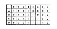
これに対して、デコード回路16では、例えば図3の表に示すように、それぞれタップ信号の波形の高電位を「1」、低電位を「0」として表したそれぞれのパターンで、表の上部に示す数値に変換が行われるようにする。これによって、クロック信号の1周期を8分割した値が形成され、クロック周波数を上げずに積分型A/D変換器の分解能を向上させることができる。 On the other hand, in the
すなわち、例えば図1のような4段のリング発振器34の場合は、カウンタ12に入力される信号Aの他にB、C、Dの信号が得られる。これらの信号は周波数が同一で、位相が異なっている。ここでカウンタ12の1LSBに相当する時間はクロック信号の1周期の時間であるが、これらの位相が異なった信号をラッチ回路15に入力し、比較器11からのトリガー信号によりラッチすればより高い分解能を得ることができる。 That is, for example, in the case of the four-stage ring oscillator 34 as shown in FIG. 1, B, C, and D signals are obtained in addition to the signal A input to the
そこで、例えば図3の表において、トリガー信号によりラッチ回路15の出力が、A=1、B=1、C=1、D=0になった場合は、3ビット単位の「3」という状態であることがわかる。そこでデコード回路16においてこのラッチ回路15の出力をデコードすれば、適切なバイナリー信号が得られる。この方法を用いることで変換周波数が同一であっても分解能を上げ、消費電力を低減させることができる。 Therefore, for example, in the table of FIG. 3, when the output of the
一方、通常の積分型A/D変換器では、変換周波数fcにてNビットの分解能を得るために必要なクロック周波数fclkは、数3式のようになる。 On the other hand, in a normal integration type A / D converter, the clock frequency fclk required to obtain N-bit resolution at the conversion frequency fc is expressed by the following equation (3).
ここで、消費電力の大半がカウンタ12で消費されるとすれば、その消費電力Pdは、
これに対し、本例では、ラッチ回路15による分解能をM(ビット)として、その変換周波数 fclk′は、
また、消費電力Pd′は
従って、従来と本発明を採用した場合の消費電力比率は、
ここで、例えばN=14、M=3ビットとすると、クロック周波数は0.125倍、消費電力は0.13倍となり、大幅なクロック周波数と消費電力の低減が図られることになる。また、これによりクロック周波数を高くすることなくA/D変換器の分解能を向上させることができる。なお、〔数9〕の式の左辺をf(14,M)と置いてグラフで描くと図4に示すようになり、特にM=6以下での効果が明らかである。 Here, for example, if N = 14 and M = 3 bits, the clock frequency is 0.125 times and the power consumption is 0.13 times, and the clock frequency and power consumption are greatly reduced. In addition, the resolution of the A / D converter can be improved without increasing the clock frequency. In addition, when the left side of the formula of [Equation 9] is set to f (14, M) and plotted in a graph, it becomes as shown in FIG.
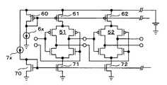
さらに図5には、CMOSを用いてリング発振器を形成した場合の具体例を示す。図5に示されている回路では、それぞれCMOS素子4個からなる差動アンプ51、52を縦続に接続している。なお、図5では2段接続された例を示しているが、実際にはさらに多段が接続される。すなわち、上述の実施形態例(図1のリング発信器34を参照)では、このような差動アンプが4段接続され、最終段の差動アンプの出力が初段の入力に帰還されている。 Further, FIG. 5 shows a specific example in which a ring oscillator is formed using CMOS. In the circuit shown in FIG. 5,
そして、これらの差動アンプ51、52のソース側、及びドレイン側に設けられる電流源61、62及び電流源71、72の電流値が、それぞれカレントミラー回路60、70を介して共通に制御できるようにされる。これによって、カレントミラー回路60、70の電流源6x、7xの電流値を外部から制御することで、差動アンプ51、52が縦続に接続された回路全体の遅延量の調整を行うことができる。 The current values of the
このようにしてリング発振器が形成される。そして、本例のようにリング型発振器として、差動型の遅延要素(差動アンプ)を用いる場合には、遅延要素の段数を偶数段にすることが可能となり、デコード回路16での、特に2進数への変換を容易に行うことができる。また、この回路構成では、個々の遅延要素の遅延量にばらつきの生じる可能性があるが、このようなばらつきは一般的に10%未満であり、1/8の分解能を求める場合では問題の無いものである。 In this way, a ring oscillator is formed. When a differential delay element (differential amplifier) is used as a ring oscillator as in this example, the number of stages of delay elements can be an even number. Conversion to binary numbers can be easily performed. Further, in this circuit configuration, there is a possibility that the delay amount of each delay element may vary, but such variation is generally less than 10%, and there is no problem when a resolution of 1/8 is obtained. Is.
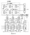
また、図6は、本発明を適用したA/D変換器を有する撮像装置の一実施形態例の構成を示すブロック図である。この図6に基づいて、本例のA/D変換器を有する撮像装置の全体について、その概略を説明する。 FIG. 6 is a block diagram showing a configuration of an embodiment of an imaging apparatus having an A / D converter to which the present invention is applied. Based on this FIG. 6, the outline is demonstrated about the whole imaging device which has an A / D converter of this example.
図6において、撮像装置は撮像部100を有し、この撮像部100には水平選択線Ha、Hb…と垂直出力線Va、Vb…が縦横に配設され、その各交点に画素Pが設けられる。そして、基準信号源101によって駆動される水平選択回路102で形成される水平選択信号が、水平選択線Ha、Hb…に供給され、選択された水平選択線Ha、Hb…に接続された画素Pの受光信号が、垂直出力線Va、Vb…に取り出される。 6, the imaging apparatus has an
これらの垂直出力線Va、Vb…に取り出された受光信号がそれぞれ比較器103a、103b…に供給され、これらの比較器103a、103b…には、基準信号源101によって駆動されるランプ信号発生回路104で形成されるランプ信号が供給される。そして、これらの比較器103a、103b…の比較極性が反転した瞬間に、トリガー信号がカウンタ105a、105b…に供給される。 The received light signals taken out to the vertical output lines Va, Vb,... Are supplied to the
また、基準信号源101からの基準信号が位相周波数比較器(PFD)106に供給され、この位相周波数比較器106の出力がリング発振器107に供給されると共に、リング発振器107からの信号が位相周波数比較器106に帰還される。これによって、位相ロックループ回路が形成される。なお、図6の回路は概略を示したもので、実際の位相ロックループ回路は、図1に示したように形成されるものである。 Further, a reference signal from the
そして、リング発振器107のタップ信号A〜Dがラッチ及びデコード回路108a、108b…に共通に供給され、これらのラッチ及びデコード回路108a、108b…に比較器103a、103b…からのトリガー信号が供給される。また、タップ信号Aがカウンタ105a、105b…に供給される。これらのカウンタ105a、105b…と、ラッチ及びデコード回路108a、108b…の信号が出力ライン17に取り出される。 The tap signals A to D of the
これによって、図1に示したのと同等のA/D変換器を有する撮像装置が形成される。従って、この実施の形態例においても、クロックパルス周波数を上げることなく高分解能化を図ることができ、特に撮像装置においては、高画質化、高速化を実現することができ、さらに、クロック生成の困難を生じないため、高分解能化を容易に実現できると共に、低消費電力化も図ることができる。 Thereby, an imaging apparatus having an A / D converter equivalent to that shown in FIG. 1 is formed. Therefore, also in this embodiment, high resolution can be achieved without increasing the clock pulse frequency, and particularly in the imaging apparatus, high image quality and high speed can be realized, and further, clock generation can be achieved. Since there is no difficulty, high resolution can be easily realized and low power consumption can be achieved.
さらに本発明によるA/D変換器を有する撮像装置は、携帯電話機などの撮像機能を有する電子機器においても広く応用可能とされるものである。ここで図7には、応用の一例として、携帯電話機に適用した場合の実施の形態例の構成をブロック図で示す。 Furthermore, the imaging apparatus having an A / D converter according to the present invention can be widely applied to electronic devices having an imaging function such as a mobile phone. Here, FIG. 7 is a block diagram showing a configuration of an embodiment when applied to a mobile phone as an example of application.
すなわち図7の携帯電話機においては、マイク音声増幅部201に供給された音声信号はA/D変換器202でデジタル信号に変換されて主制御部203に入力される。そして主制御部203からの信号は、圧縮伸張部204、ベースバンド処理部205、変復調部206を通じて送信部207に供給され、アンテナ共用部208を通じてアンテナ209から送信される。 That is, in the mobile phone of FIG. 7, the audio signal supplied to the microphone
また、アンテナ209とアンテナ共用部208で受信された信号から、受信部210で所望の信号が取り出される。この取り出された信号は、シンセサイザ部211、変復調部206、ベースバンド処理部205、圧縮伸張部204を通じて主制御部203に供給される。また、タイミング制御部212によってシンセサイザ部211、ベースバンド処理部205、圧縮伸張部204での処理動作が制御される。そして主制御部203からの信号が、D/A変換器213でアナログ信号に変換されて音声拡声部214に出力される。 In addition, a desired signal is extracted by the receiving
なお、主制御部203には記憶部215が設けられて処理中のデータが記憶される。また、キー入力部216からの信号が主制御部203に供給されて、発呼時のダイアリングや受信時の許可などの制御が行われる。さらに主制御部203からの信号が表示制御部217を通じてLCD部218に供給され、各種の表示が行われる。また、これらの回路には電源制御部219から電源が供給されている。 The
以上の構成によって携帯電話機が形成される。このような携帯電話機において、近年では、撮像装置220が設けられることが多くなってきている。この撮像装置220にはカメラ撮像部221とA/D変換器222が設けられ、撮像制御部223によって撮像された画像信号が取り出されて主制御部203に供給されるようになされている。そしてこのような撮像装置220において、A/D変換器222に本発明が適用される。 A mobile phone is formed by the above configuration. In recent years, such mobile phones are often provided with an
従って、このような撮像機能を有する電子機器に本発明の積分型A/D変換器を用いた場合には、電力消費を大幅に削減することができる。そこで本発明は、特に携帯用を含む電子機器に適用した場合に有効となるものである。 Therefore, when the integral A / D converter of the present invention is used in an electronic apparatus having such an imaging function, power consumption can be greatly reduced. Therefore, the present invention is particularly effective when applied to electronic devices including portable devices.
なお本発明は、上述の説明した実施形態に限定されるものではなく、特許請求の範囲の記載を逸脱しない範囲において、種々の変形が可能とされるものである。 The present invention is not limited to the above-described embodiments, and various modifications can be made without departing from the scope of the claims.
11…比較器、12…カウンタ、13…位相ロックループ回路、14a〜14d…バッファ、15…ラッチ回路、16…デコード回路、17…出力ライン、31…位相周波数比較器(PFD)、32…チャージポンプ回路(CP)、33…ローパスフィルタ(LPF)、34…リング発振器、35…バッファ、36…1/N分周器、41〜44…差動型の遅延要素 DESCRIPTION OF
Claims (5)
Translated fromJapanese前記リング発振器は複数段の遅延要素を縦続に接続して形成され、
前記縦続に接続された各段の遅延要素の信号を前記比較器の出力が反転したタイミングで保持する保持手段と、
前記保持された前記各段の遅延要素の信号のパターンを任意の数値にデコードするデコード手段と、
前記デコード手段のデコード値を前記カウンタの計数値の下位に追加して取り出す出力手段と
を設けたことを特徴とする積分型A/D変換器。A clock signal formed by a comparator that compares a reference voltage of a ramp waveform whose voltage value linearly changes with time and an input signal and a phase locked loop circuit including a ring oscillator is counted for each period of the ramp waveform. An integration type A / D converter that takes out the count value of the counter when the output of the comparator is inverted and outputs it as a digital conversion output,
The ring oscillator is formed by cascading multiple stages of delay elements,
Holding means for holding the signal of the delay element of each stage connected in cascade at the timing when the output of the comparator is inverted;
Decoding means for decoding the held delay element signal pattern of each stage into an arbitrary numerical value;
An integration type A / D converter comprising: output means for adding and extracting the decode value of the decode means in the lower order of the count value of the counter.
ことを特徴とする請求項1記載の積分型A/D変換器。The integral A / D converter according to claim 1, wherein the plurality of stages of delay elements are formed by cascading even-numbered differential delay elements.
前記位相ロックループ回路からのクロック信号と前記各段の遅延要素の出力とを前記複数組の構成に共通に供給する
ことを特徴とする請求項1記載の積分型A/D変換器。A plurality of sets of a comparator, a counter, a holding unit, and a decoding unit are provided in parallel,
2. The integrating A / D converter according to claim 1, wherein the clock signal from the phase-locked loop circuit and the output of the delay element at each stage are supplied in common to the plurality of sets.
前記A/D変換器は、
前記受光信号を時間とともに電圧値が直線的に変化するランプ波形の参照電圧と比較する比較器と、
複数段の遅延要素を縦続に接続して形成したリング発振器を含む位相ロックループ回路と、
前記位相ロックループ回路によって形成されるクロック信号を前記ランプ波形の周期ごとに計数して前記比較器の出力が反転したときの計数値を取り出すカウンタと、
前記各段の遅延要素の信号を前記比較器の出力が反転したタイミングで保持する保持手段と、
前記保持された前記各段の遅延要素の信号のパターンを任意の数値にデコードするデコード手段と、を有し、
前記デコード手段のデコード値を前記カウンタの計数値の下位に追加して前記デジタル値として出力する
ことを特徴とするA/D変換器を有する撮像装置。An image pickup apparatus having light receiving elements arranged vertically and horizontally and having an A / D converter in which an A / D converter is provided for each vertical array of the light receiving elements so that a light reception signal is output as a digital value. There,
The A / D converter is
A comparator that compares the received light signal with a reference voltage of a ramp waveform whose voltage value changes linearly with time;
A phase-locked loop circuit including a ring oscillator formed by cascading multiple stages of delay elements;
A counter that counts a clock signal formed by the phase-locked loop circuit for each period of the ramp waveform and extracts a count value when the output of the comparator is inverted;
Holding means for holding the signal of the delay element of each stage at the timing when the output of the comparator is inverted;
Decoding means for decoding the held delay element signal pattern of each stage into an arbitrary numerical value,
An image pickup apparatus having an A / D converter, wherein the decode value of the decoding means is added to the lower order of the count value of the counter and output as the digital value.
Priority Applications (1)
| Application Number | Priority Date | Filing Date | Title |
|---|---|---|---|
| JP2006268170AJP2008092091A (en) | 2006-09-29 | 2006-09-29 | Integrating A / D Converter, Imaging Device Having A / D Converter, and Electronic Device |
Applications Claiming Priority (1)
| Application Number | Priority Date | Filing Date | Title |
|---|---|---|---|
| JP2006268170AJP2008092091A (en) | 2006-09-29 | 2006-09-29 | Integrating A / D Converter, Imaging Device Having A / D Converter, and Electronic Device |
Publications (1)
| Publication Number | Publication Date |
|---|---|
| JP2008092091Atrue JP2008092091A (en) | 2008-04-17 |
Family
ID=39375798
Family Applications (1)
| Application Number | Title | Priority Date | Filing Date |
|---|---|---|---|
| JP2006268170APendingJP2008092091A (en) | 2006-09-29 | 2006-09-29 | Integrating A / D Converter, Imaging Device Having A / D Converter, and Electronic Device |
Country Status (1)
| Country | Link |
|---|---|
| JP (1) | JP2008092091A (en) |
Cited By (25)
| Publication number | Priority date | Publication date | Assignee | Title |
|---|---|---|---|---|
| CN101873136A (en)* | 2009-04-24 | 2010-10-27 | 索尼公司 | Integrating AD converter, solid-state imaging device, and camera system |
| JP2011055196A (en)* | 2009-09-01 | 2011-03-17 | Olympus Corp | A/d converter, and solid-state imaging apparatus |
| JP2012191359A (en)* | 2011-03-09 | 2012-10-04 | Sony Corp | A/d conversion device, a/d conversion method and program |
| US8284285B2 (en) | 2010-02-03 | 2012-10-09 | Sony Corporation | Duty correction circuit, delay locked loop circuit, column A/D converter, solid-state imaging device and camera system |
| US20120318958A1 (en)* | 2011-04-11 | 2012-12-20 | Olympus Corporation | Clock generation circuit and imaging device |
| JP2014064243A (en)* | 2012-09-24 | 2014-04-10 | Olympus Corp | Data processing circuit and solid state imaging device |
| JP2014064059A (en)* | 2012-09-19 | 2014-04-10 | Olympus Corp | Ad conversion circuit and solid state imaging device |
| US8823575B2 (en) | 2012-10-04 | 2014-09-02 | Olympus Corporation | Ad conversion circuit and solid-state image pickup device |
| US8941765B2 (en) | 2012-03-22 | 2015-01-27 | Olympus Corporation | Imaging device |
| US8941045B2 (en) | 2012-04-25 | 2015-01-27 | Renesas Electronics Corporation | Solid-state imaging apparatus |
| US9030588B2 (en) | 2012-08-06 | 2015-05-12 | Olympus Corporation | Imaging apparatus for reducing deterioration of AD conversion of a pixel signal |
| JP2015128278A (en)* | 2013-11-27 | 2015-07-09 | ソニー株式会社 | A / D conversion device, gray code generation device, signal processing device, imaging device, and electronic device |
| US9106860B2 (en) | 2012-08-03 | 2015-08-11 | Olympus Corporation | AD conversion circuit and solid-state image pickup device |
| US9204076B2 (en) | 2013-09-13 | 2015-12-01 | Olympus Corporation | Imaging apparatus |
| US9204070B2 (en) | 2010-06-01 | 2015-12-01 | Sony Corporation | Integrating A/D converter, integrating A/D conversion method, solid-state imaging device and camera system |
| US9392204B2 (en) | 2013-02-13 | 2016-07-12 | Olympus Corporation | Image capturing device |
| JP2017123613A (en)* | 2016-01-08 | 2017-07-13 | 国立大学法人北海道大学 | A / D (Analog / Digital) conversion circuit and A / D conversion method |
| CN108055040A (en)* | 2017-12-19 | 2018-05-18 | 上海集成电路研发中心有限公司 | A kind of ADC structures and its D conversion method based on multiphase clock |
| CN108551344A (en)* | 2018-03-29 | 2018-09-18 | 上海集成电路研发中心有限公司 | Double sampled analog-to-digital conversion circuit |
| US10367519B2 (en) | 2017-10-11 | 2019-07-30 | Tech Idea Co., Ltd. | Time domain A/D converter group and sensor device using the same |
| JP2020096300A (en)* | 2018-12-13 | 2020-06-18 | ルネサスエレクトロニクス株式会社 | Semiconductor device and system |
| JP2020182210A (en)* | 2017-10-11 | 2020-11-05 | 株式会社テックイデア | Time domain A / D converter group and sensor device using this |
| US11233967B2 (en) | 2018-02-01 | 2022-01-25 | Olympus Corporation | AD conversion circuit, imaging device, and endoscope system |
| CN115250337A (en)* | 2021-04-27 | 2022-10-28 | 联咏科技股份有限公司 | Column Analog-to-Digital Converter and Its Local Notation |
| US12040813B2 (en) | 2021-09-22 | 2024-07-16 | Renesas Electronics Corporation | Integrating analog-to-digital converter and semiconductor device |
- 2006
- 2006-09-29JPJP2006268170Apatent/JP2008092091A/enactivePending
Cited By (41)
| Publication number | Priority date | Publication date | Assignee | Title |
|---|---|---|---|---|
| CN101873136A (en)* | 2009-04-24 | 2010-10-27 | 索尼公司 | Integrating AD converter, solid-state imaging device, and camera system |
| JP2010258817A (en)* | 2009-04-24 | 2010-11-11 | Sony Corp | Integrating AD converter, solid-state imaging device, and camera system |
| US8456554B2 (en) | 2009-04-24 | 2013-06-04 | Sony Corporation | Integrated AD converter, solid state imaging device, and camera system |
| CN101873136B (en)* | 2009-04-24 | 2013-07-24 | 索尼公司 | Integrated AD converter, solid state imaging device, and camera system |
| JP2011055196A (en)* | 2009-09-01 | 2011-03-17 | Olympus Corp | A/d converter, and solid-state imaging apparatus |
| US8885081B2 (en) | 2009-09-01 | 2014-11-11 | Olympus Corporation | A/D converter and solid-state imaging apparatus |
| US8284285B2 (en) | 2010-02-03 | 2012-10-09 | Sony Corporation | Duty correction circuit, delay locked loop circuit, column A/D converter, solid-state imaging device and camera system |
| US9204070B2 (en) | 2010-06-01 | 2015-12-01 | Sony Corporation | Integrating A/D converter, integrating A/D conversion method, solid-state imaging device and camera system |
| JP2012191359A (en)* | 2011-03-09 | 2012-10-04 | Sony Corp | A/d conversion device, a/d conversion method and program |
| US8729946B2 (en)* | 2011-04-11 | 2014-05-20 | Olympus Corporation | Clock generation circuit and imaging device |
| US20120318958A1 (en)* | 2011-04-11 | 2012-12-20 | Olympus Corporation | Clock generation circuit and imaging device |
| US8941765B2 (en) | 2012-03-22 | 2015-01-27 | Olympus Corporation | Imaging device |
| US9369653B2 (en) | 2012-04-25 | 2016-06-14 | Renesas Electronics Corporation | Solid-state imaging apparatus |
| US8941045B2 (en) | 2012-04-25 | 2015-01-27 | Renesas Electronics Corporation | Solid-state imaging apparatus |
| US9258507B2 (en) | 2012-04-25 | 2016-02-09 | Renesas Electronics Corporation | Solid-state imaging apparatus |
| US9106860B2 (en) | 2012-08-03 | 2015-08-11 | Olympus Corporation | AD conversion circuit and solid-state image pickup device |
| US9030588B2 (en) | 2012-08-06 | 2015-05-12 | Olympus Corporation | Imaging apparatus for reducing deterioration of AD conversion of a pixel signal |
| US9106253B2 (en) | 2012-09-19 | 2015-08-11 | Olympus Corporation | AD conversion circuit and solid-state imaging apparatus |
| JP2014064059A (en)* | 2012-09-19 | 2014-04-10 | Olympus Corp | Ad conversion circuit and solid state imaging device |
| JP2014064243A (en)* | 2012-09-24 | 2014-04-10 | Olympus Corp | Data processing circuit and solid state imaging device |
| US8823575B2 (en) | 2012-10-04 | 2014-09-02 | Olympus Corporation | Ad conversion circuit and solid-state image pickup device |
| US9392204B2 (en) | 2013-02-13 | 2016-07-12 | Olympus Corporation | Image capturing device |
| US9204076B2 (en) | 2013-09-13 | 2015-12-01 | Olympus Corporation | Imaging apparatus |
| JP2015128278A (en)* | 2013-11-27 | 2015-07-09 | ソニー株式会社 | A / D conversion device, gray code generation device, signal processing device, imaging device, and electronic device |
| US10334195B2 (en) | 2013-11-27 | 2019-06-25 | Sony Corporation | A/D conversion device, gray code generation device, signal processing device, imaging element, and electronic device |
| US10659710B2 (en) | 2013-11-27 | 2020-05-19 | Sony Corporation | A/D conversion device, gray code generation device, signal processing device, imaging element, and electronic device |
| JP2017123613A (en)* | 2016-01-08 | 2017-07-13 | 国立大学法人北海道大学 | A / D (Analog / Digital) conversion circuit and A / D conversion method |
| JP2020182210A (en)* | 2017-10-11 | 2020-11-05 | 株式会社テックイデア | Time domain A / D converter group and sensor device using this |
| US10367519B2 (en) | 2017-10-11 | 2019-07-30 | Tech Idea Co., Ltd. | Time domain A/D converter group and sensor device using the same |
| US10382051B2 (en) | 2017-10-11 | 2019-08-13 | Tech Idea Co., Ltd. | Time domain A/D converter group and sensor device using the same |
| CN108055040B (en)* | 2017-12-19 | 2021-08-31 | 上海集成电路研发中心有限公司 | A kind of ADC structure based on multi-phase clock and its analog-to-digital conversion method |
| CN108055040A (en)* | 2017-12-19 | 2018-05-18 | 上海集成电路研发中心有限公司 | A kind of ADC structures and its D conversion method based on multiphase clock |
| US11233967B2 (en) | 2018-02-01 | 2022-01-25 | Olympus Corporation | AD conversion circuit, imaging device, and endoscope system |
| CN108551344A (en)* | 2018-03-29 | 2018-09-18 | 上海集成电路研发中心有限公司 | Double sampled analog-to-digital conversion circuit |
| CN108551344B (en)* | 2018-03-29 | 2022-04-01 | 上海集成电路研发中心有限公司 | Double-sampling analog-to-digital conversion circuit |
| JP2020096300A (en)* | 2018-12-13 | 2020-06-18 | ルネサスエレクトロニクス株式会社 | Semiconductor device and system |
| US11115614B2 (en) | 2018-12-13 | 2021-09-07 | Renesas Electronics Corporation | Image sensor with A/D conversion circuit having reduced DNL deterioration |
| CN115250337A (en)* | 2021-04-27 | 2022-10-28 | 联咏科技股份有限公司 | Column Analog-to-Digital Converter and Its Local Notation |
| CN115250337B (en)* | 2021-04-27 | 2025-04-18 | 联咏科技股份有限公司 | Column analog-to-digital converter and its local counting method |
| US12040813B2 (en) | 2021-09-22 | 2024-07-16 | Renesas Electronics Corporation | Integrating analog-to-digital converter and semiconductor device |
| JP7650766B2 (en) | 2021-09-22 | 2025-03-25 | ルネサスエレクトロニクス株式会社 | Integral A/D converter and semiconductor device |
Similar Documents
| Publication | Publication Date | Title |
|---|---|---|
| JP2008092091A (en) | Integrating A / D Converter, Imaging Device Having A / D Converter, and Electronic Device | |
| US10659710B2 (en) | A/D conversion device, gray code generation device, signal processing device, imaging element, and electronic device | |
| US7859583B2 (en) | Solid-state image capture device, analog/digital conversion method for solid state image capture device, and image capture device | |
| US9806721B2 (en) | Multiple data rate counter, data converter including the same, and image sensor including the same | |
| US8085329B2 (en) | Solid-state imaging device, driving control method, and imaging apparatus | |
| JP4289206B2 (en) | Counter circuit | |
| US7969469B2 (en) | Multiple image sensor system with shared processing | |
| CN103716553B (en) | Photoelectric conversion device and imaging system | |
| US20150237288A1 (en) | Solid-state image sensing apparatus | |
| EP3116217A1 (en) | Imaging element, control method, and imaging device | |
| WO2012017730A1 (en) | Time detection circuit, ad converter, and solid state imaging device | |
| TW201029335A (en) | Analog-to-digital converter, solid-state imaging device including the same, and method of digitizing analog signal | |
| US20160116936A1 (en) | Data interface and data transmission method | |
| US20120112940A1 (en) | Analog to digital converter | |
| WO2017183117A1 (en) | A/d converter, solid-state imaging device, method for driving solid-state imaging device, and electronic apparatus | |
| CN102832936A (en) | AD conversion circuit and imaging apparatus | |
| US7683972B2 (en) | Video signal processing apparatus which generates plural clocks and performing video signal processing using the plural clocks | |
| JP2011250009A (en) | Data selection circuit, data transfer circuit, ramp wave generation circuit, and solid state image sensor | |
| JP2006303752A (en) | Imaging device | |
| US20080062311A1 (en) | Methods and Devices to Use Two Different Clocks in a Television Digital Encoder | |
| KR20160027870A (en) | Data interface and data transmit method | |
| US7548265B2 (en) | Image pickup apparatus and image pickup method including clocks | |
| US20080062312A1 (en) | Methods and Devices of Using a 26 MHz Clock to Encode Videos |