JP2008091808A - Semiconductor integrated circuit - Google Patents
Semiconductor integrated circuitDownload PDFInfo
- Publication number
- JP2008091808A JP2008091808AJP2006273579AJP2006273579AJP2008091808AJP 2008091808 AJP2008091808 AJP 2008091808AJP 2006273579 AJP2006273579 AJP 2006273579AJP 2006273579 AJP2006273579 AJP 2006273579AJP 2008091808 AJP2008091808 AJP 2008091808A
- Authority
- JP
- Japan
- Prior art keywords
- wiring
- circuit
- esd
- integrated circuit
- power supply
- Prior art date
- Legal status (The legal status is an assumption and is not a legal conclusion. Google has not performed a legal analysis and makes no representation as to the accuracy of the status listed.)
- Pending
Links
Images


Classifications
- H—ELECTRICITY
- H10—SEMICONDUCTOR DEVICES; ELECTRIC SOLID-STATE DEVICES NOT OTHERWISE PROVIDED FOR
- H10D—INORGANIC ELECTRIC SEMICONDUCTOR DEVICES
- H10D89/00—Aspects of integrated devices not covered by groups H10D84/00 - H10D88/00
- H10D89/60—Integrated devices comprising arrangements for electrical or thermal protection, e.g. protection circuits against electrostatic discharge [ESD]
- H10D89/601—Integrated devices comprising arrangements for electrical or thermal protection, e.g. protection circuits against electrostatic discharge [ESD] for devices having insulated gate electrodes, e.g. for IGFETs or IGBTs
Landscapes
- Semiconductor Integrated Circuits (AREA)
- Design And Manufacture Of Integrated Circuits (AREA)
- Metal-Oxide And Bipolar Metal-Oxide Semiconductor Integrated Circuits (AREA)
Abstract
Translated fromJapaneseDescription
Translated fromJapanese本発明は、半導体集積回路において、静電気放電(ESD;electrostatic discharge)の耐性を改善する技術に関する。 The present invention relates to a technique for improving resistance to electrostatic discharge (ESD) in a semiconductor integrated circuit.
一般に、半導体集積回路には、特定の機能を実現するための機能回路を、入出力端子を通して印加される静電気サージから保護するため、ESD保護回路が設けられる。たとえば、下記特許文献1に開示された半導体集積回路では、機能回路の外部に、サージ電流を流すための保護素子(トランジスタ)を含むESD保護回路が形成される。かかるESD保護回路は、機能回路の外部において、電源端子と接地端子間にサージ電流を誘導し、機能回路に印加される電圧を制限するように設計される。
しかしながら、従来のESD保護回路を備えた半導体集積回路では、実際には、電源端子と接地端子間のサージ電流経路が有するインピーダンスが大きいために、機能回路に印加される電圧が機能回路のブレークダウン電圧よりも高くなって、機能回路が破壊する場合がある。このような場合には、たとえば保護素子としてのトランジスタを再設計することになるため、半導体集積回路の下地層のマスクをすべて作り直さなければならなかった。したがって、マスクを作り直すことなく、必要に応じて静電気放電の耐性を向上させることが可能となる半導体集積回路が望まれていた。 However, in a conventional semiconductor integrated circuit equipped with an ESD protection circuit, the surge current path between the power supply terminal and the ground terminal has a large impedance, so that the voltage applied to the functional circuit is a breakdown of the functional circuit. It may be higher than the voltage and the functional circuit may be destroyed. In such a case, for example, a transistor as a protection element is redesigned, so that all the masks for the base layer of the semiconductor integrated circuit have to be remade. Therefore, there has been a demand for a semiconductor integrated circuit that can improve the resistance to electrostatic discharge as needed without remaking the mask.
本発明の半導体集積回路は、入出力端子と、基準電位と1または複数の電源電位とに接続されて動作するセルベースの機能回路と、静電気検出部と、機能回路内において各電源電位に対応して設けられ、機能回路を静電気放電から保護するための複数の保護用セルと、を備える。静電気検出部は、入出力端子に対する静電気放電の印加を検出する。各保護用セルは、基準電位と対応する電源電位との間に接続されるトランジスタを含む。
この発明の半導体集積回路では、各保護用セルと静電気検出部とを接続し、静電気検出部による静電気放電の検出を受けて各保護用セルのトランジスタを導通させるための配線層が形成される。The semiconductor integrated circuit according to the present invention corresponds to each power supply potential in an input / output terminal, a cell-based functional circuit operating by being connected to a reference potential and one or more power supply potentials, an electrostatic detection unit, and the functional circuit. And a plurality of protection cells for protecting the functional circuit from electrostatic discharge. The static electricity detection unit detects application of electrostatic discharge to the input / output terminals. Each protection cell includes a transistor connected between a reference potential and a corresponding power supply potential.
In the semiconductor integrated circuit according to the present invention, a wiring layer is formed for connecting each protection cell and the static electricity detector, and detecting the electrostatic discharge by the static electricity detector to make the transistor of each protective cell conductive.
この発明の半導体集積回路によれば、配線層の設計変更のみによって、ESD耐性を向上させることができる。したがって、基本的なESD保護機能を有するトランジスタを形成する下地層のマスクを作り直すという設計変更が必要ない。 According to the semiconductor integrated circuit of the present invention, the ESD resistance can be improved only by changing the design of the wiring layer. Therefore, there is no need for a design change in which a mask for a base layer for forming a transistor having a basic ESD protection function is recreated.
本発明の半導体集積回路によれば、マスクを作り直すことなく、必要に応じて静電気放電の耐性を向上させることが可能となる。 According to the semiconductor integrated circuit of the present invention, it is possible to improve the resistance to electrostatic discharge as needed without remaking the mask.
<第1の実施形態>
本発明の第1の実施形態について説明する前に、本発明の理解のため、本発明の第1の実施形態の参照回路としての半導体集積回路(集積回路2)について説明する。<First Embodiment>
Before describing the first embodiment of the present invention, a semiconductor integrated circuit (integrated circuit 2) as a reference circuit according to the first embodiment of the present invention will be described in order to understand the present invention.
[集積回路2(参照回路)]
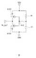
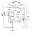
図1は、この集積回路2の回路構成を示す平面図である。集積回路2は、特定の機能を実現するための機能回路4が中心に配置され、その機能回路4の周囲に、入出力端子(パッドP1,P2、VDD端子(電源電位VDD)、GND端子(接地電位GND)等)とESD保護回路とが設けられる。
機能回路4はセルベースの集積回路である。一般に、セルベースの集積回路には、配線のみで論理を変更できるように未使用のセルが配置され、また、電源と接地間のノイズを除去するためのデカップリング容量を含むセル等が配置されている。[Integrated circuit 2 (reference circuit)]
FIG. 1 is a plan view showing a circuit configuration of the integrated
The functional circuit 4 is a cell-based integrated circuit. In general, in a cell-based integrated circuit, unused cells are arranged so that the logic can be changed only by wiring, and cells including a decoupling capacitor for removing noise between the power supply and the ground are arranged. ing.
以下、集積回路2のESD保護回路について説明する。このESD保護回路は、配線L0,L1と、ダイオードD1〜D4と、ESDトリガ検出回路10(静電気検出部)と、NMOSトランジスタQ1とを含む。
リング状の配線L0(接地配線)は、機能回路4の周囲に設けられ、GND端子に接続される。リング状の配線L1(電源配線)は、配線L0の周囲に設けられ、VDD端子に接続される。
パッドP1から機能回路4への配線LP1上のノードN1には、ダイオードD1,D2が接続される。すなわち、ダイオードD1のアノードがノードN1に接続され、ダイオードD1のカソードが配線L1に接続される。ダイオードD2のアノードが配線L0に接続され、ダイオードD2のカソードがノードN1に接続される。
パッドP2から機能回路4への配線LP2上のノードN2には、ダイオードD3,D4が接続される。すなわち、ダイオードD3のアノードがノードN2に接続され、ダイオードD3のカソードが配線L1に接続される。ダイオードD4のアノードが配線L0に接続され、ダイオードD4のカソードがノードN2に接続される。Hereinafter, the ESD protection circuit of the integrated
The ring-shaped wiring L0 (ground wiring) is provided around the functional circuit 4 and connected to the GND terminal. The ring-shaped wiring L1 (power supply wiring) is provided around the wiring L0 and connected to the VDD terminal.
Diodes D1 and D2 are connected to a node N1 on the wiring LP1 from the pad P1 to the functional circuit 4. That is, the anode of the diode D1 is connected to the node N1, and the cathode of the diode D1 is connected to the wiring L1. The anode of the diode D2 is connected to the wiring L0, and the cathode of the diode D2 is connected to the node N1.
Diodes D3 and D4 are connected to the node N2 on the wiring LP2 from the pad P2 to the functional circuit 4. That is, the anode of the diode D3 is connected to the node N2, and the cathode of the diode D3 is connected to the wiring L1. The anode of diode D4 is connected to line L0, and the cathode of diode D4 is connected to node N2.
NMOSトランジスタQ1は、配線L0と配線L1との間に設けられる。すなわち、NMOSトランジスタQ1のドレインは配線L1(電源電位VDD)に接続され、ソースは配線L0(接地電位GND)に接続されている。NMOSトランジスタQ1のゲートは、ESDトリガ検出回路10の出力端子TR_OUTに接続される。このNMOSトランジスタQ1は、ESDトリガ検出回路10の出力端子TR_OUTがハイレベル(Hレベル)になるとオンし、ESDによるサージ電流を配線L1から配線L0へ導く役割を有している。 The NMOS transistor Q1 is provided between the wiring L0 and the wiring L1. That is, the drain of the NMOS transistor Q1 is connected to the wiring L1 (power supply potential VDD), and the source is connected to the wiring L0 (ground potential GND). The gate of the NMOS transistor Q1 is connected to the output terminal TR_OUT of the ESD
ESDトリガ検出回路10は、配線L1と配線L0との間に設けられ、電源電位VDDによって動作する。ESDトリガ検出回路10は、入出力端子を介したESDイベントの発生を検出する回路である。
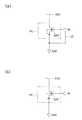
図2は、ESDトリガ検出回路10の一例を示す回路図である。図2におけるVDD端子およびGND端子は、機能回路4に適用する際には、それぞれ配線L1および配線L0に接続される。図2に示したESDトリガ検出回路10は、VDD端子とGND端子との間に直列に接続された抵抗R1およびキャパシタC1と、インバータを構成するPMOSトランジスタQ101およびNMOSトランジスタQ102とを有する。キャパシタC1の一端(正極側)に設けられたノードN10がインバータに対する入力となる。インバータの出力は、ESDトリガ検出回路10の出力端子TR_OUTとなる。
このESDトリガ検出回路10において、抵抗R1およびキャパシタC1はローパスフィルタ(LPF)を構成するが、そのLPFの時定数(C1×R1)は、ESDの発生に伴ってVDD端子に印加される急峻な電圧上昇の影響を受けないような大きな値に設定される。The ESD
FIG. 2 is a circuit diagram showing an example of the ESD
In the ESD
このESDトリガ検出回路10の動作について図3を参照して説明する。図3は、(a)ESDサージ電流波形と、(b)各部の電圧波形とを示している。図3(a)に示すESDサージ電流波形は、公的試験方法であるHBM(Human Body Model)試験に規定されている波形である。また、図3では、ESDイベントが発生した時刻をt0としている。
ESDイベントが発生し、図3(a)に示したESDサージ電流が機能回路4の配線L1に発生すると、図3(b)に示すように、図2におけるVDD端子の電圧も同様に、時刻t0から急峻に上昇する。一方、抵抗R1およびキャパシタC1で構成されるLPFの時定数が大きいために、ノードN10の電圧は、図3(b)に示すように、VDD端子における急峻な電圧変化に追従せず、緩やかに上昇する。その結果、ESDイベントの発生後、ESDトリガ検出回路10のインバータ入力はローレベル(Lレベル)に維持され、インバータ出力である出力端子TR_OUTの電圧はHレベルに維持される。すなわち、出力端子TR_OUTの電圧は、図3(b)に示すように、ほぼVDD端子の電圧レベルと同等となる。The operation of the ESD
When an ESD event occurs and the ESD surge current shown in FIG. 3A occurs in the wiring L1 of the functional circuit 4, as shown in FIG. 3B, the voltage at the VDD terminal in FIG. It rises steeply from t0. On the other hand, since the time constant of the LPF composed of the resistor R1 and the capacitor C1 is large, the voltage at the node N10 does not follow a steep voltage change at the VDD terminal as shown in FIG. To rise. As a result, after the occurrence of the ESD event, the inverter input of the ESD
次に、集積回路2のESD保護動作について、図4を参照して説明する。
図4は、集積回路2の入出力端子にESDイベントが発生したときのESDサージ電流の流れを示す図である。なお、図4では、パッドP1にESDイベントが発生した場合を想定している。
図4に示すように、パッドP1にESDイベントが発生すると、パッドP1から流れるESDサージ電流は、ノードN1を介してダイオードD1を順方向に流れた後、配線L1を流れる。配線L1の電圧上昇に伴い、ESDトリガ検出回路10の出力端子TR_OUTがHレベルになるとNMOSトランジスタQ1がオンするので、配線L1と配線L0とが短絡する。これにより、配線L1を流れるサージ電流は、配線L0に導かれるとともに、順方向に接続されたダイオードD4と、ノードN2とを介して、接地されたパッドP2に流れ込む。なお、このESDイベント発生時、機能回路4内においても電流が消費されるが、その電流はNMOSトランジスタQ1を流れるサージ電流と比較して非常に小さい。Next, the ESD protection operation of the integrated
FIG. 4 is a diagram showing the flow of an ESD surge current when an ESD event occurs at the input / output terminal of the integrated
As shown in FIG. 4, when an ESD event occurs in the pad P1, the ESD surge current flowing from the pad P1 flows in the forward direction through the diode D1 via the node N1, and then flows through the wiring L1. The NMOS transistor Q1 is turned on when the output terminal TR_OUT of the ESD
上述したように、パッドP1にESDイベントが発生した場合、そのESDサージ電流は、図4に示すように、その大部分が機能回路4の周囲に設けられた配線L0,L1を流れる。そして、このESDサージ電流が流れている間、機能回路4に印加される電圧が、機能回路4のブレークダウン電圧に達することがないように設計される。 As described above, when an ESD event occurs in the pad P1, most of the ESD surge current flows through the wirings L0 and L1 provided around the functional circuit 4 as shown in FIG. The voltage applied to the functional circuit 4 is designed not to reach the breakdown voltage of the functional circuit 4 while the ESD surge current is flowing.
ところで、集積回路2を製造し、実際にESD試験を実施すると、図4に示したサージ電流の電流経路におけるインピーダンスが高いことに起因して、機能回路4に印加される電圧がブレークダウン電圧を越え、機能回路4が破壊に至る場合がある。通常、ESD試験は、完成した集積回路2に対して行われるが、その完成した集積回路2のESD耐性が低いことが判明した場合には、NMOSトランジスタQ1やダイオードの設計変更を行うことが必要であるため、集積回路2の下地層のマスクをすべて作り直さなければならない。 By the way, when the
[集積回路1(第1の実施形態)の構成]
次に、第1の実施形態の集積回路1の構成について、図5および図6を参照して説明する。
以下に説明する本発明の第1の実施形態の半導体集積回路は、上記集積回路2(参照回路)とは異なり、一旦完成した後にESD耐性が低いことは判明した場合であっても、下地層のマスクを作り直すことなく、小規模の設計変更によってESDの耐性を向上させることが可能となっている。具体的には、第1の実施形態の半導体集積回路は、下地層のマスクを変更することなく、上層の金属配線層のみを変更することで、ESD耐性を向上させることが可能である。[Configuration of Integrated Circuit 1 (First Embodiment)]
Next, the configuration of the
The semiconductor integrated circuit according to the first embodiment of the present invention to be described below is different from the integrated circuit 2 (reference circuit) described above, even if it is found that the ESD resistance is low after being completed, Thus, it is possible to improve ESD resistance by a small design change without remaking the mask. Specifically, the semiconductor integrated circuit according to the first embodiment can improve the ESD resistance by changing only the upper metal wiring layer without changing the mask of the underlying layer.
図5および図6は、本実施形態の集積回路1の回路構成を示す平面図であるが、図1に示した集積回路2と同一の部位については、同一の符号を付して重複説明を行わない。なお、図5は、保護用セルPC(後述する)を無効にした場合を示し、図6は、保護用セルPCを有効にした場合を示す。 5 and 6 are plan views showing the circuit configuration of the
本実施形態の集積回路1は、機能回路の内部のセル群の一部に、機能回路をESDイベントから保護するための保護用セルPCを設ける点で、集積回路2と異なる。図5に示す集積回路1では、機能回路5内に7個の保護用セルPC_1〜PC_7が形成されている。この保護用セルPCは、機能回路5内の空きセル領域を利用して予め作りこんでおく。
図6に示すように、各保護用セルPCと、ESDトリガ検出回路10の出力端子TR_OUTとは、集積回路1の金属配線層において配線LSを設けることによって、必要に応じて接続可能であり、これにより保護用セルPCを有効化できるようになっている。すなわち、配線LSを結線しない状態で集積回路1が完成した後、この集積回路のESD保護回路(前述した集積回路2と同一の保護機能)のみで十分なESD耐性が確保されていることが判明した場合には、各保護用セルPCと、ESDトリガ検出回路10の出力端子TR_OUTとを接続しない。逆に、配線LSを結線しない状態で集積回路1が完成した後、この集積回路のESD保護回路のみで十分なESD耐性が確保されていないことが判明した場合には、各保護用セルPCと、ESDトリガ検出回路10の出力端子TR_OUTとを配線LSによって接続して、各保護用セルPCを動作可能な状態にする。The
As shown in FIG. 6, each protection cell PC and the output terminal TR_OUT of the ESD
保護用セルPCは、ESDイベントが発生したときに、配線L1を流れるサージ電流をGND端子へ引き込むことができるように設計される。
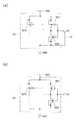
この保護用セルPCのいくつかの回路構成例について、図7〜9を参照して説明する。図7〜9は、保護用セルPCの一例を示す回路図であって、(a)は、保護用セルPCを無効にした場合の配線を含む図、(b)は、保護用セルPCを有効にした場合の配線を含む図を示す。The protection cell PC is designed so that a surge current flowing through the wiring L1 can be drawn into the GND terminal when an ESD event occurs.
Several circuit configuration examples of the protection cell PC will be described with reference to FIGS. 7 to 9 are circuit diagrams showing an example of the protection cell PC, where (a) is a diagram including wiring when the protection cell PC is invalidated, and (b) is an illustration of the protection cell PC. The figure including the wiring when enabled is shown.
この集積回路1では、図7〜9の各図の(a)に示すような配線の状態で、保護用セルPCが機能回路5の空きセル領域に予め形成されている。そして、この配線の状態でESD試験を行い、十分なESD耐性が確保されていないことが判明した場合には、集積回路1の配線層の設計変更を行って、各図の(b)に示すような配線の状態にする。すなわち、その配線層の設計変更では、各図の(a)に示す配線LD(保護用セルPCの入力端子INとGND端子とを結ぶ配線)を除去し、ESDトリガ検出回路10の出力端子TR_OUTと保護用セルPCの入力端子INとの間の配線LS(図6参照)を設ける。
図7〜9の各図の(a)に示す状態では、保護用セルPCの入力端子INは常に接地電位となっており、保護用セルPCは機能しない。In the
7A to 9A, the input terminal IN of the protection cell PC is always at the ground potential, and the protection cell PC does not function.
以下、保護用セルPCが機能する場合、すなわち、ESDトリガ検出回路10の出力端子TR_OUTと各保護用セルPCの入力端子INとの間の配線LSが設けられ、かつ、各保護用セルPCの配線が図7〜9の(b)に示すような場合について、保護用セルPCの構成および動作について順に説明する。 Hereinafter, when the protection cell PC functions, that is, the wiring LS between the output terminal TR_OUT of the ESD
図7に例示する保護用セルPCは、単一のNMOSトランジスタQ20のみによって構成される。NMOSトランジスタQ20のドレインは、VDD端子に接続される。すなわち、NMOSトランジスタQ20のドレインは、機能回路5の周囲の配線L1に接続されているのと等価である。NMOSトランジスタQ20のソースは、GND端子に接続される。NMOSトランジスタQ20のゲートは、入力端子INを介して、ESDトリガ検出回路10の出力端子TR_OUTに接続される。したがって、ESDトリガ検出回路10にてESDイベントが検出され、その出力端子TR_OUTがHレベルになると、保護用セルPC内のNMOSトランジスタQ20がオンし、配線L1に流れるサージ電流をGND端子へ引き込む。 The protection cell PC illustrated in FIG. 7 includes only a single NMOS transistor Q20. The drain of the NMOS transistor Q20 is connected to the VDD terminal. That is, the drain of the NMOS transistor Q20 is equivalent to being connected to the wiring L1 around the
図8に例示する保護用セルPCは、インバータを構成するPMOSトランジスタQ21およびNMOSトランジスタQ22と、PMOSトランジスタQ23とを有する。インバータの入力には入力端子INが接続され、インバータの出力はPMOSトランジスタQ23のゲートに接続される。PMOSトランジスタQ23のソースは、VDD端子に接続される。すなわち、NMOSトランジスタQ20のソースは、機能回路5の周囲の配線L1に接続されているのと等価である。PMOSトランジスタQ23のドレインは、GND端子に接続される。この保護用セルPCのインバータ入力は、入力端子INを介して、ESDトリガ検出回路10の出力端子TR_OUTに接続される。したがって、ESDトリガ検出回路10にてESDイベントが検出され、その出力端子TR_OUTがHレベルになると、インバータの出力がLレベルとなって、PMOSトランジスタQ23がオンし、配線L1に流れるサージ電流をGND端子へ引き込む。 The protection cell PC illustrated in FIG. 8 includes a PMOS transistor Q21 and an NMOS transistor Q22 that form an inverter, and a PMOS transistor Q23. The input terminal IN is connected to the input of the inverter, and the output of the inverter is connected to the gate of the PMOS transistor Q23. The source of the PMOS transistor Q23 is connected to the VDD terminal. That is, the source of the NMOS transistor Q20 is equivalent to being connected to the wiring L1 around the
図9に例示する保護用セルPCは、図8に示した保護用セルPCと比較すると、NMOSトランジスタQ24が追加された点でのみ異なる。このNMOSトランジスタQ24のドレインは、PMOSトランジスタQ23のドレインと接続される。NMOSトランジスタQ24のソースは、GND端子に接続される。NMOSトランジスタQ24のゲートは、保護用セルPCの入力端子INに接続される。この保護用セルPCでは、ESDトリガ検出回路10の出力端子TR_OUTがHレベルのときには、PMOSトランジスタQ23およびNMOSトランジスタQ24がともにオンし、配線L1に流れるサージ電流をGND端子へ引き込む。 The protection cell PC illustrated in FIG. 9 is different from the protection cell PC illustrated in FIG. 8 only in that an NMOS transistor Q24 is added. The drain of the NMOS transistor Q24 is connected to the drain of the PMOS transistor Q23. The source of the NMOS transistor Q24 is connected to the GND terminal. The gate of the NMOS transistor Q24 is connected to the input terminal IN of the protection cell PC. In this protection cell PC, when the output terminal TR_OUT of the ESD
なお、図8および図9に例示した保護用セルPCでは、入力部にインバータを設けているが、入力端子INの論理レベル(すなわち、ESDトリガ検出回路10の出力端子TR_OUTの論理レベル)を反転できるゲート回路(論理回路)であればよく、たとえばNAND回路やNOR回路によって形成することもできる。
また、図7に示した保護用セルPCの回路は、電流駆動能力が大きいNMOSトランジスタのみで構成されており、電流駆動能力およびセルの占有面積を考慮すると最も好ましい。In the protection cell PC illustrated in FIGS. 8 and 9, an inverter is provided in the input unit, but the logic level of the input terminal IN (that is, the logic level of the output terminal TR_OUT of the ESD trigger detection circuit 10) is inverted. Any gate circuit (logic circuit) can be used. For example, the gate circuit (logic circuit) can be formed by a NAND circuit or a NOR circuit.
Further, the circuit of the protection cell PC shown in FIG. 7 includes only NMOS transistors having a large current driving capability, and is most preferable in consideration of the current driving capability and the cell occupation area.
[集積回路1の動作]
次に、機能回路5内の保護用セルPCを有効にした場合の集積回路1のESD保護動作について、図10を参照して説明する。
図10は、集積回路1の入出力端子にESDイベントが発生したときのESDサージ電流の流れを示す図である。なお、図10では、パッドP1にESDイベントが発生した場合を想定している。
図10に示すように、パッドP1にESDイベントが発生すると、パッドP1から流れるESDサージ電流は、ノードN1を介してダイオードD1を順方向に流れた後、配線L1を流れる。配線L1の電圧上昇に伴い、ESDトリガ検出回路10の出力端子TR_OUTがHレベルになるとNMOSトランジスタQ1がオンするので、配線L1と配線L0とが短絡する。これにより、配線L1を流れるサージ電流は、配線L0に導かれるとともに、順方向に接続されたダイオードD4とノードN2とを介して、接地されたパッドP2に流れ込む。[Operation of Integrated Circuit 1]
Next, the ESD protection operation of the
FIG. 10 is a diagram illustrating the flow of an ESD surge current when an ESD event occurs at the input / output terminal of the
As shown in FIG. 10, when an ESD event occurs in the pad P1, the ESD surge current flowing from the pad P1 flows in the forward direction through the diode D1 via the node N1, and then flows through the wiring L1. The NMOS transistor Q1 is turned on when the output terminal TR_OUT of the ESD
一方、ESDトリガ検出回路10の出力端子TR_OUTがHレベルになると、機能回路5内の各保護用セルPC_1〜PC_7内におけるVDD端子とGND端子間のトランジスタ(たとえば図7に例示した保護用セルPCでは、NMOSトランジスタQ20に相当)がオンするので、配線L1を流れるサージ電流の一部は、配線LSを通して、各保護用セルからGND端子へ流れ込む。
このように、機能回路5内の保護用セルPCを有効にした場合の集積回路1では、パッドP1から流れるESDのサージ電流は、機能回路5の周囲の電流経路だけではなく、機能回路5内部の保護用セルPCを経由した複数の電流経路に分散してGND端子に放出されるので、保護用セルPCを無効にした場合(配線LSを結線しない場合)と比較して、機能回路5のESD耐性が向上する。On the other hand, when the output terminal TR_OUT of the ESD
As described above, in the
以上説明したように、本実施形態の集積回路1によれば、機能回路5内の空きセル領域に予め保護用セルPCを作りこんでおき、必要に応じて、配線層の設計変更のみによって集積回路のESD耐性を向上させることができる。したがって、一旦完成した集積回路に対してESD試験を行い、その完成した集積回路のESD耐性が低いことが判明した場合であっても、集積回路の下地層のマスクを作り直すという設計変更が必要ない。 As described above, according to the
なお、本実施形態の集積回路1において、ESDトリガ検出回路10を含め、NMOSトランジスタQ1を含むESD保護回路が機能回路5の外部に設けられているが、これに限られず、機能回路5内部に設けてもよい。 In the
また、本実施形態の集積回路1において、機能回路5の外部に設けられたESD保護回路は一例に過ぎず、その他のESD保護回路を適用することもできる。すなわち、本実施形態において、機能回路5の外部に設けられたESD保護回路は、基本的なESD保護機能を備えた回路を実現するための一例に過ぎず、その基本的なESD保護機能から、配線層のみの変更によってさらに高いESD保護機能を備えた集積回路へと、比較的簡便に変更できる点が本発明の主旨である。
したがって、図5における保護用セルPC_1〜PC_7の中の1つの保護用セルのみの入力端子INと、ESDトリガ検出回路10の出力端子TR_OUTとを予め結線しておき、ESD試験の評価結果次第で、残りの保護用セルの入力端子INを出力端子TR_OUTと結線することによりESD耐性を高めるようにしてもよい。かかる構成では、図5におけるNMOSトランジスタQ1は必要ない。In the
Therefore, the input terminal IN of only one protection cell among the protection cells PC_1 to PC_7 in FIG. 5 and the output terminal TR_OUT of the ESD
[変形例]
以下、本実施形態の集積回路における、保護用セルPCの好ましい配置について、図11を参照して説明する。図11は、第1の実施形態の集積回路の好ましい回路構成を示す平面図である。
図11に示す集積回路において、機能回路5内の保護用セルPCが形成される領域(保護用セル領域)は、機能回路5の領域(コア領域)の端部に配置される。図11では、ESDトリガ検出回路10を含む領域(静電気検出領域)は、コア領域よりも外部に形成されているが、コア領域の内部に形成されていてもよい。
このように、各保護用セルPCを機能回路5の領域の端部に配置することで、VDD端子とGND端子間の電流経路の総和を最短とすることができる。したがって、ESDイベントが発生した際のサージ電流を流れる経路のインピーダンスを極力小さくすることができるので、保護用セルをコア領域内にランダムに配置した場合と比較して、集積回路のESD耐性をさらに向上させることが可能となる。[Modification]
Hereinafter, a preferred arrangement of the protection cells PC in the integrated circuit of this embodiment will be described with reference to FIG. FIG. 11 is a plan view showing a preferred circuit configuration of the integrated circuit of the first embodiment.
In the integrated circuit shown in FIG. 11, the region (protective cell region) in which the protective cell PC is formed in the
Thus, by arranging each protection cell PC at the end of the area of the
<第2の実施形態>
次に、本発明の半導体集積回路の第2の実施形態について説明する。この第2の実施形態の半導体集積回路(後述する集積回路3)は、機能回路の内部が2電源によって動作する点で、第1の実施形態の集積回路1と異なる。2電源で動作する半導体集積回路は、近年では比較的一般的な構成となりつつある。たとえば、外部機器とのインタフェースを行う入出力部は3.3Vの電源電圧で動作し、その他の内部回路は1.2Vの電源電圧で動作するというような半導体集積回路の設計が行われる。<Second Embodiment>
Next, a second embodiment of the semiconductor integrated circuit of the present invention will be described. The semiconductor integrated circuit (integrated
[集積回路3(第2の実施形態)の構成]
以下、第2の実施形態の集積回路3の構成について、図12および図13を参照して説明する。この集積回路3は、第1の電源電位VDD1と第2の電源電位VDD2の2電源によって動作する。
図12および図13は、本実施形態の集積回路3の回路構成を示す平面図である。なお、図12は、保護用セルPCを無効にした場合を示し、図13は、保護用セルPCを有効にした場合を示す。[Configuration of Integrated Circuit 3 (Second Embodiment)]
Hereinafter, the configuration of the
12 and 13 are plan views showing the circuit configuration of the
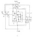
図12に示す集積回路3は、特定の機能を実現するための機能回路6が中心に配置され、その機能回路6の周囲に、入出力端子(パッドP3,P4、VDD1端子(電源電位VDD1)、VDD2端子(電源電位VDD2)、GND端子(接地電位GND)等)とESD保護回路とが設けられる。機能回路6はセルベースの集積回路である。 In the
以下、集積回路3のESD保護回路について説明する。このESD保護回路は、配線L0,L1,L2と、ダイオードD5〜D8と、ESDトリガ検出回路10,11(静電気検出部)と、NMOSトランジスタQ1,Q2とを含む。
リング状の配線L0(接地配線)は、機能回路6の周囲に設けられ、GND端子に接続される。リング状の配線L1(電源配線)は、配線L0の周囲に設けられ、VDD1端子に接続される。リング状の配線L2(電源配線)は、配線L1の周囲に設けられ、VDD2端子に接続される。すなわち、配線L1,L2は、配線L0の周囲において、機能回路6が形成される領域(コア領域)の外側に向かって順に、2つの電源電位VDD1,VDD2の各々に対応して接続されるようにして設けられている。Hereinafter, the ESD protection circuit of the
The ring-shaped wiring L0 (ground wiring) is provided around the
パッドP3から機能回路6への配線LP3上には、バッファBUF1が設けられる。この配線LP3上のノードN3には、ダイオードD5,D6が接続される。すなわち、ダイオードD5のアノードがノードN3に接続され、ダイオードD5のカソードが配線L2に接続される。ダイオードD6のアノードが配線L0に接続され、ダイオードD6のカソードがノードN3に接続される。
パッドP4から機能回路6への配線LP4上には、バッファBUF2が設けられる。この配線LP4上のノードN4には、ダイオードD7,D8が接続される。すなわち、ダイオードD7のアノードがノードN4に接続され、ダイオードD7のカソードが配線L1に接続される。ダイオードD8のアノードが配線L0に接続され、ダイオードD8のカソードがノードN4に接続される。A buffer BUF1 is provided on the wiring LP3 from the pad P3 to the
A buffer BUF2 is provided on the wiring LP4 from the pad P4 to the
ESDトリガ検出回路11は、配線L1と配線L0との間に設けられ、電源電位VDD1によって動作する。ESDトリガ検出回路12は、配線L2と配線L0との間に設けられ、電源電位VDD2によって動作する。ESDトリガ検出回路11,12は、入出力端子を介したESDイベントの発生を検出する回路である。なお、各ESDトリガ検出回路は、図2に示したESDトリガ検出回路10と同様の回路で構成することができる。 The ESD
NMOSトランジスタQ11は、配線L0と配線L1との間に設けられる。すなわち、NMOSトランジスタQ11のドレインは配線L1(電源電位VDD1)に接続され、ソースは配線L0(接地電位GND)に接続されている。NMOSトランジスタQ11のゲートは、ESDトリガ検出回路11の出力端子TR_OUT1に接続される。このNMOSトランジスタQ11は、ESDトリガ検出回路11の出力端子TR_OUT1がハイレベル(Hレベル)になるとオンし、ESDによるサージ電流を配線L1から配線L0へ導く役割を有している。 The NMOS transistor Q11 is provided between the wiring L0 and the wiring L1. That is, the drain of the NMOS transistor Q11 is connected to the wiring L1 (power supply potential VDD1), and the source is connected to the wiring L0 (ground potential GND). The gate of the NMOS transistor Q11 is connected to the output terminal TR_OUT1 of the ESD
NMOSトランジスタQ12は、配線L0と配線L2との間に設けられる。すなわち、NMOSトランジスタQ12のドレインは配線L2(電源電位VDD2)に接続され、ソースは配線L0(接地電位GND)に接続されている。NMOSトランジスタQ12のゲートは、ESDトリガ検出回路12の出力端子TR_OUT2に接続される。このNMOSトランジスタQ12は、ESDトリガ検出回路12の出力端子TR_OUT2がハイレベル(Hレベル)になるとオンし、ESDによるサージ電流を配線L2から配線L0へ導く役割を有している。 The NMOS transistor Q12 is provided between the wiring L0 and the wiring L2. That is, the drain of the NMOS transistor Q12 is connected to the wiring L2 (power supply potential VDD2), and the source is connected to the wiring L0 (ground potential GND). The gate of the NMOS transistor Q12 is connected to the output terminal TR_OUT2 of the ESD
図12に示す集積回路3では、機能回路6内の第1のサブ領域61に3個の保護用セルPC_11〜PC_13が配置され、機能回路6内の第2のサブ領域62に4個の保護用セルPC_21〜PC_24が配置されている。なお、第1のサブ領域61は、機能回路6内において、電源電位VDD1にて動作するセルが形成されている領域である。第2のサブ領域62は、機能回路6内において、電源電位VDD2にて動作するセルが形成されている領域である。保護用セルは、各サブ領域の空きセル領域を利用して予め作りこんでおく。
なお、保護用セルPC_11〜PC_13の各々は、図7〜9に示した保護用セルと同様の回路を、電源電位VDD1で動作するように構成して実現することができる。保護用セルPC_21〜PC_24の各々は、図7〜9に示した保護用セルと同様の回路を、電源電位VDD2で動作するように構成して実現することができる。In the
Note that each of the protection cells PC_11 to PC_13 can be realized by configuring a circuit similar to the protection cell shown in FIGS. 7 to 9 to operate at the power supply potential VDD1. Each of the protection cells PC_21 to PC_24 can be realized by configuring a circuit similar to the protection cell shown in FIGS. 7 to 9 to operate at the power supply potential VDD2.
第1の実施形態と同様に、各保護用セルPCと、ESDトリガ検出回路11,12の出力端子TR_OUT1,TR_OUT2とは、集積回路3の金属配線層において、それぞれ配線LS1,LS2を設けることによって、必要に応じて接続可能であり、これにより保護用セルPCを有効化できるようになっている(図13参照)。集積回路3が動作する2つの電源電位ごとに、すなわち、コア領域内のサブ領域ごとに独立に、保護用セルPCを有効化または無効化することができるように構成されている。 As in the first embodiment, each protection cell PC and the output terminals TR_OUT1 and TR_OUT2 of the ESD
[集積回路3の動作]
次に、機能回路6内の保護用セルPCを有効にした場合の集積回路3のESD保護動作について、図14を参照して説明する。
図14は、集積回路1の入出力端子にESDイベントが発生したときのESDサージ電流の流れを示す図である。なお、図14では、VDD1端子にESDイベントが発生した場合を想定している。
図14に示すように、VDD1端子にESDイベントが発生すると、VDD1端子の電圧上昇し、ESDトリガ検出回路11の出力端子TR_OUT1がHレベルになるので、NMOSトランジスタQ1がオンする。したがって、ESDのサージ電流は、NMOSトランジスタQ11のドレインからソースに向かって流れた後、配線L0を経由して、接地されたGND端子に流れ込む。[Operation of Integrated Circuit 3]
Next, the ESD protection operation of the
FIG. 14 is a diagram illustrating the flow of an ESD surge current when an ESD event occurs at the input / output terminal of the
As shown in FIG. 14, when an ESD event occurs at the VDD1 terminal, the voltage at the VDD1 terminal rises and the output terminal TR_OUT1 of the ESD
一方、ESDトリガ検出回路11の出力端子TR_OUT1がHレベルになると、第1のサブ領域61内の各保護用セルPC_11〜PC_13内のトランジスタ(たとえば図7に例示した保護用セルPCでは、NMOSトランジスタQ20に相当)がオンするので、サージ電流の一部は、配線LS1を通して、各保護用セルからGND端子へ流れ込む。
このように、第1のサブ領域61内の保護用セルPCを有効にした場合の集積回路3では、VDD1端子から流れるESDのサージ電流は、機能回路6の周囲の電流経路だけではなく、第1のサブ領域61内の保護用セルPCを経由した複数の電流経路に分散してGND端子に放出されるので、保護用セルPCを無効にした場合(配線LS1を結線しない場合)と比較して、機能回路6のESD耐性が向上する。On the other hand, when the output terminal TR_OUT1 of the ESD
As described above, in the
以上、VDD1端子にESDイベントが発生した場合について説明したが、同様のことがVDD2端子ついても言える。すなわち、第2のサブ領域62内の保護用セルPCを有効にした場合の集積回路3では、VDD2端子から流れるESDのサージ電流は、機能回路6の周囲の電流経路だけではなく、第2のサブ領域62内の保護用セルPC_21〜PC_24を経由した複数の電流経路に分散してGND端子に放出されるので、保護用セルPCを無効にした場合(配線LS2を結線しない場合)と比較して、機能回路6のESD耐性が向上する。 Although the case where an ESD event occurs at the VDD1 terminal has been described above, the same can be said for the VDD2 terminal. That is, in the
なお、集積回路3において、パッドP3,P4にESDイベントが発生した場合には、機能回路6の外部のサージ電流経路は、第1の実施形態において説明したのと同様である。
たとえばパッドP3にESDイベントが発生した場合、図15に示すようにサージ電流が流れる。すなわち、パッドP3から流れるESDサージ電流は、ノードN3およびバッファを介してダイオードD5を順方向に流れた後、配線L2を流れる。配線L2の電圧上昇に伴い、ESDトリガ検出回路12の出力端子TR_OUT2がHレベルになるとNMOSトランジスタQ12がオンするので、配線L2と配線L0とが短絡する。これにより、配線L2を流れるサージ電流は、配線L0に導かれるとともに、順方向に接続されたダイオードD8とノードN4とを介してGND端子に流れ込む。その際、サージ電流は、第2のサブ領域62内の保護用セルPC_21〜PC_24を経由した複数の電流経路に分散してGND端子に放出される。In the
For example, when an ESD event occurs in the pad P3, a surge current flows as shown in FIG. That is, the ESD surge current flowing from the pad P3 flows through the diode L5 in the forward direction via the node N3 and the buffer, and then flows through the wiring L2. When the output terminal TR_OUT2 of the ESD
以上説明したように、本実施形態の集積回路3は、機能回路6が2電源によって動作し、機能回路6内において異なる電源電位によって動作する領域(第1のサブ領域61、第2のサブ領域62)の各々の空きセル領域に、予め保護用セルPCを作り込まれる。したがって、第1の実施形態と同様、必要に応じて、配線層の設計変更のみによって集積回路のESD耐性を向上させることができる。したがって、一旦完成した集積回路に対してESD試験を行い、その完成した集積回路のESD耐性が低いことが判明した場合であっても、集積回路の下地層のマスクを作り直すという設計変更が必要ない。 As described above, in the
[変形例]
以下、本実施形態の集積回路における、保護用セルPCの好ましい配置について、図16を参照して説明する。図16は、第2の実施形態の集積回路の好ましい回路構成を示す平面図である。
図16に示す集積回路において、機能回路6内の保護用セルPCが形成される領域(保護用セル領域)は、機能回路6の領域(コア領域)内において、2つの電源電位VDD1,VDD2で動作するサブ領域61,62の端部に配置される。図16において、保護用セルPC1は電源電位VDD1で動作するセルであり、保護用セルPC2は電源電位VDD2で動作するセルである。ESDトリガ検出回路11,12を含む領域(静電気検出領域)は、図16ではコア領域よりも外部に形成されているが、コア領域の内部に形成されていてもよい。
このように、各保護用セルPCを機能回路6内の各サブ領域の端部に配置することで、VDD1端子とGND端子間の電流経路、および、VDD2端子とGND端子間の電流経路の総和を最短とすることができる。したがって、ESDイベントが発生した際のサージ電流を流れる経路のインピーダンスを極力小さくすることができるので、保護用セルをコア領域内にランダムに配置した場合と比較して、集積回路のESD耐性をさらに向上させることが可能となる。[Modification]
Hereinafter, a preferred arrangement of the protection cells PC in the integrated circuit of the present embodiment will be described with reference to FIG. FIG. 16 is a plan view showing a preferred circuit configuration of the integrated circuit of the second embodiment.
In the integrated circuit shown in FIG. 16, the region (protective cell region) in which the protective cell PC in the
Thus, by arranging each protection cell PC at the end of each sub-region in the
以上、本発明の実施の形態を詳述してきたが、具体的な構成及びシステムは本実施の形態に限られるものではなく、本発明の要旨を逸脱しない範囲の設計変更や、他のシステムへの適応なども含まれる。
たとえば、第2の実施形態では2電源によって動作する半導体集積回路について説明したが、この技術分野の当業者であれば、上述した各実施形態の記載に基づいて3電源以上で動作する半導体集積回路へ容易に拡張することが可能であることは明らかである。The embodiment of the present invention has been described in detail above, but the specific configuration and system are not limited to the present embodiment, and design modifications and other systems can be made without departing from the scope of the present invention. This includes adaptations.
For example, in the second embodiment, a semiconductor integrated circuit that operates with two power supplies has been described. However, those skilled in the art will understand that a semiconductor integrated circuit that operates with three or more power supplies based on the description of each embodiment described above. Obviously, it can be easily extended to.
1〜3…集積回路(半導体集積回路)
4〜6…機能回路
PC…保護用セル
L0〜L2…配線
10〜12…ESDトリガ検出回路(静電気検出部)1-3. Integrated circuit (semiconductor integrated circuit)
4 to 6 Functional circuit PC Protection cell L0 to
Claims (5)
Translated fromJapanese基準電位と1または複数の電源電位とに接続されて動作するセルベースの機能回路と、
前記入出力端子に対する静電気放電の印加を検出する静電気検出部と、
前記機能回路内において各電源電位に対応して設けられ、前記機能回路を静電気放電から保護するための複数の保護用セルであって、各保護用セルが前記基準電位と対応する電源電位との間に接続されるトランジスタを含む複数の保護用セルと、
を備え、
各保護用セルと前記静電気検出部とを接続し、前記静電気検出部による静電気放電の検出を受けて各保護用セルのトランジスタを導通させるための配線層が形成される
半導体集積回路。Input and output terminals;
A cell-based functional circuit operating in connection with a reference potential and one or more power supply potentials;
A static electricity detector for detecting the application of electrostatic discharge to the input / output terminals;
A plurality of protection cells provided in the functional circuit corresponding to each power supply potential and protecting the functional circuit from electrostatic discharge, each protection cell having a power supply potential corresponding to the reference potential A plurality of protective cells including transistors connected therebetween;
With
A semiconductor integrated circuit in which each protection cell is connected to the static electricity detection unit, and a wiring layer is formed for conducting a transistor of each protection cell upon detection of electrostatic discharge by the static electricity detection unit.
前記コア領域の周囲に配置され、前記基準電位に接続されるリング形状の接地配線と、
前記接地配線の周囲において、前記コア領域の外側に向かって順に配置され、前記1または複数の電源電位の各々に対応して接続される、リング形状の1または複数の電源配線と、
前記1または複数の電源配線の外部に配置される入出力端子と、
前記機能回路の内部または外部において、前記接地配線と、前記電源配線の各々との間に接続され、前記入出力端子に対する静電気放電を検出する1または複数の静電気検出部、が形成される静電気検出領域と、
前記機能回路内において各電源配線に対応して設けられ、前記機能回路を静電気放電から保護するための複数の保護用セルであって、各保護用セルが前記接地配線と対応する電源配線との間に接続されるトランジスタを含む複数の保護用セル、が形成される保護用セル領域と、
を備え、
前記保護用セルと前記静電気検出部とを接続し、静電気検出部による静電気放電の検出を受けて各保護用セルのトランジスタを導通させるための配線層が形成される
半導体集積回路。A core region in which a cell-based functional circuit operating by being connected to a reference potential and one or more power supply potentials is formed;
A ring-shaped ground wiring disposed around the core region and connected to the reference potential;
Around the ground wiring, one or more ring-shaped power supply wirings arranged in order toward the outside of the core region and connected corresponding to each of the one or more power supply potentials;
An input / output terminal arranged outside the one or more power supply wirings;
Static electricity detection in which one or a plurality of static electricity detection parts are formed inside or outside the functional circuit and connected between the ground wiring and each of the power supply wirings to detect electrostatic discharge with respect to the input / output terminals. Area,
A plurality of protection cells provided corresponding to each power supply wiring in the functional circuit and protecting the functional circuit from electrostatic discharge, each protection cell being connected to the ground wiring and the corresponding power supply wiring. A protective cell region in which a plurality of protective cells including transistors connected therebetween are formed;
With
A semiconductor integrated circuit in which the protection cell and the static electricity detection portion are connected, and a wiring layer is formed for conducting the transistor of each protection cell upon detection of electrostatic discharge by the static electricity detection portion.
前記保護用セルは、対応する電源配線と同一の電源電位で動作するサブ領域の端部に配置される
請求項2記載の半導体集積回路。The core region has one or more subregions for each power supply potential at which the functional circuit operates,
The semiconductor integrated circuit according to claim 2, wherein the protection cell is disposed at an end of a sub-region that operates at the same power supply potential as the corresponding power supply wiring.
請求項1〜3のいずれかに記載の半導体集積回路。The semiconductor integrated circuit according to claim 1, wherein the protection cell includes an NMOS transistor.
請求項4記載の半導体集積回路。The semiconductor integrated circuit according to claim 4, wherein the protection cell further includes a logic circuit that inverts a signal from the static electricity detection unit.
Priority Applications (2)
| Application Number | Priority Date | Filing Date | Title |
|---|---|---|---|
| JP2006273579AJP2008091808A (en) | 2006-10-05 | 2006-10-05 | Semiconductor integrated circuit |
| US11/769,124US20080084641A1 (en) | 2006-10-05 | 2007-06-27 | Semiconductor integrated circuit |
Applications Claiming Priority (1)
| Application Number | Priority Date | Filing Date | Title |
|---|---|---|---|
| JP2006273579AJP2008091808A (en) | 2006-10-05 | 2006-10-05 | Semiconductor integrated circuit |
Publications (1)
| Publication Number | Publication Date |
|---|---|
| JP2008091808Atrue JP2008091808A (en) | 2008-04-17 |
Family
ID=39274762
Family Applications (1)
| Application Number | Title | Priority Date | Filing Date |
|---|---|---|---|
| JP2006273579APendingJP2008091808A (en) | 2006-10-05 | 2006-10-05 | Semiconductor integrated circuit |
Country Status (2)
| Country | Link |
|---|---|
| US (1) | US20080084641A1 (en) |
| JP (1) | JP2008091808A (en) |
Cited By (3)
| Publication number | Priority date | Publication date | Assignee | Title |
|---|---|---|---|---|
| JP2014511576A (en)* | 2011-03-01 | 2014-05-15 | クアルコム,インコーポレイテッド | Distributed building block of RC clamp circuit in semiconductor die core region |
| CN108650560A (en)* | 2018-05-17 | 2018-10-12 | 郑州云海信息技术有限公司 | A kind of network interface and optimization method for taking into account electromagnetic compatibility and signal integrity |
| JP2023110556A (en)* | 2022-01-28 | 2023-08-09 | ローム株式会社 | semiconductor integrated circuit |
Families Citing this family (5)
| Publication number | Priority date | Publication date | Assignee | Title |
|---|---|---|---|---|
| JPWO2007055047A1 (en)* | 2005-11-10 | 2009-04-30 | シャープ株式会社 | Display device and electronic device including the same |
| JP2008177491A (en)* | 2007-01-22 | 2008-07-31 | Renesas Technology Corp | Semiconductor device |
| EP2246885A1 (en)* | 2009-04-27 | 2010-11-03 | STmicroelectronics SA | ESD protection structure for an integrated circuit |
| JP2011171680A (en)* | 2010-02-22 | 2011-09-01 | Panasonic Corp | Semiconductor integrated circuit device |
| US11322935B2 (en)* | 2020-09-08 | 2022-05-03 | Apple Inc. | High speed ESP protection circuit |
Family Cites Families (4)
| Publication number | Priority date | Publication date | Assignee | Title |
|---|---|---|---|---|
| US5886862A (en)* | 1997-11-26 | 1999-03-23 | Digital Equipment Corporation | Cross-referenced electrostatic discharge protection systems and methods for power supplies |
| US6476472B1 (en)* | 2000-08-18 | 2002-11-05 | Agere Systems Inc. | Integrated circuit package with improved ESD protection for no-connect pins |
| US6724603B2 (en)* | 2002-08-09 | 2004-04-20 | Motorola, Inc. | Electrostatic discharge protection circuitry and method of operation |
| JP4996057B2 (en)* | 2004-05-26 | 2012-08-08 | 旭化成エレクトロニクス株式会社 | Semiconductor circuit |
- 2006
- 2006-10-05JPJP2006273579Apatent/JP2008091808A/enactivePending
- 2007
- 2007-06-27USUS11/769,124patent/US20080084641A1/ennot_activeAbandoned
Cited By (4)
| Publication number | Priority date | Publication date | Assignee | Title |
|---|---|---|---|---|
| JP2014511576A (en)* | 2011-03-01 | 2014-05-15 | クアルコム,インコーポレイテッド | Distributed building block of RC clamp circuit in semiconductor die core region |
| KR101569669B1 (en) | 2011-03-01 | 2015-11-17 | 퀄컴 인코포레이티드 | Distributed building blocks of r-c clamping circuitry in semiconductor die core area |
| CN108650560A (en)* | 2018-05-17 | 2018-10-12 | 郑州云海信息技术有限公司 | A kind of network interface and optimization method for taking into account electromagnetic compatibility and signal integrity |
| JP2023110556A (en)* | 2022-01-28 | 2023-08-09 | ローム株式会社 | semiconductor integrated circuit |
Also Published As
| Publication number | Publication date |
|---|---|
| US20080084641A1 (en) | 2008-04-10 |
Similar Documents
| Publication | Publication Date | Title |
|---|---|---|
| JP4986459B2 (en) | Semiconductor integrated circuit device | |
| CN100359685C (en) | ESD protection circuit with control circuit | |
| JP3990352B2 (en) | Semiconductor integrated circuit device | |
| JP2008091808A (en) | Semiconductor integrated circuit | |
| JP3901671B2 (en) | Semiconductor integrated circuit device | |
| KR20130012565A (en) | Semiconductor integrated circuit | |
| JP2007234718A (en) | Semiconductor integrated circuit device | |
| JP5509573B2 (en) | Electrostatic discharge protection circuit and integrated circuit device having the same | |
| US7889469B2 (en) | Electrostatic discharge protection circuit for protecting semiconductor device | |
| JP6521792B2 (en) | Semiconductor device | |
| CN104867922B (en) | Conductor integrated circuit device and the electronic equipment for using the device | |
| US20130027824A1 (en) | Semiconductor device | |
| JP2009147040A (en) | Semiconductor integrated circuit device | |
| JPH09275191A (en) | Semiconductor integrated circuit and circuit device using the same | |
| KR20130072090A (en) | Semiconductor integrated circuit | |
| US6833590B2 (en) | Semiconductor device | |
| JP4031423B2 (en) | Semiconductor integrated circuit | |
| JP5082841B2 (en) | Semiconductor device | |
| US6583475B2 (en) | Semiconductor device | |
| JP2006210926A (en) | Semiconductor device provided with ESD protection circuit | |
| JP2011222549A (en) | Esd protection circuit and integrated circuit | |
| JP6384223B2 (en) | ESD protection circuit and integrated circuit | |
| JP2940506B2 (en) | Semiconductor device | |
| JP2009076664A (en) | ESD protection circuit | |
| JP2008227369A (en) | Electrostatic breakage protection circuit |
Legal Events
| Date | Code | Title | Description |
|---|---|---|---|
| A621 | Written request for application examination | Free format text:JAPANESE INTERMEDIATE CODE: A621 Effective date:20080922 | |
| A711 | Notification of change in applicant | Free format text:JAPANESE INTERMEDIATE CODE: A712 Effective date:20081210 | |
| A131 | Notification of reasons for refusal | Free format text:JAPANESE INTERMEDIATE CODE: A131 Effective date:20081216 | |
| A521 | Request for written amendment filed | Free format text:JAPANESE INTERMEDIATE CODE: A523 Effective date:20090205 | |
| RD03 | Notification of appointment of power of attorney | Free format text:JAPANESE INTERMEDIATE CODE: A7423 Effective date:20090205 | |
| A131 | Notification of reasons for refusal | Free format text:JAPANESE INTERMEDIATE CODE: A131 Effective date:20090303 | |
| A02 | Decision of refusal | Free format text:JAPANESE INTERMEDIATE CODE: A02 Effective date:20090630 |