JP2008078512A - Manufacturing method of semiconductor devices - Google Patents
Manufacturing method of semiconductor devicesDownload PDFInfo
- Publication number
- JP2008078512A JP2008078512AJP2006258080AJP2006258080AJP2008078512AJP 2008078512 AJP2008078512 AJP 2008078512AJP 2006258080 AJP2006258080 AJP 2006258080AJP 2006258080 AJP2006258080 AJP 2006258080AJP 2008078512 AJP2008078512 AJP 2008078512A
- Authority
- JP
- Japan
- Prior art keywords
- insulating film
- semiconductor device
- manufacturing
- tms
- film
- Prior art date
- Legal status (The legal status is an assumption and is not a legal conclusion. Google has not performed a legal analysis and makes no representation as to the accuracy of the status listed.)
- Granted
Links
Images


Landscapes
- Formation Of Insulating Films (AREA)
- Thin Film Transistor (AREA)
Abstract
Description
Translated fromJapanese本発明は、半導体装置の製法に係り、より詳しくは、絶縁膜が、PE−CVD法によってテトラメチルシラン(TMS)と亜酸化窒素(N2O)とを用いて低温度にて成膜される半導体装置の製法に関するものである。The present invention relates to a method for manufacturing a semiconductor device, and more specifically, an insulating film is formed at a low temperature using tetramethylsilane (TMS) and nitrous oxide (N2 O) by a PE-CVD method. The present invention relates to a method for manufacturing a semiconductor device.
半導体装置において、絶縁膜は多く用いられ、薄膜トランジスタ(TFT)の基板保護膜やゲート絶縁膜、MOSトランジスタのゲート酸化膜、フィールド酸化膜などの素子分離、メモリセルのキャパシタ絶縁膜、多層配線の層間を分離するための層間絶縁膜などが挙げられる。
これらの絶縁膜は、他の素子への影響から、低温で成膜することが求められている。特に、フレキシブルディスプレイなどの非耐熱及び非耐水性のプラスチック基板上でTFTアプリケーションを実用化するためには、基板保護膜(接触層がない場合)及びゲート絶縁膜の低温形成が必須である。In a semiconductor device, an insulating film is often used, and a substrate protective film and a gate insulating film of a thin film transistor (TFT), element isolation such as a gate oxide film and a field oxide film of a MOS transistor, a capacitor insulating film of a memory cell, and an interlayer of a multilayer wiring For example, an interlayer insulating film for separating the layers can be used.
These insulating films are required to be formed at a low temperature because of influence on other elements. In particular, in order to put TFT applications into practical use on non-heat-resistant and water-resistant plastic substrates such as flexible displays, it is essential to form a substrate protective film (in the case where there is no contact layer) and a gate insulating film at a low temperature.
絶縁膜の成膜方法としては、プラズマ化学気相成長(CVD)法が挙げられ、比較的低温度で成膜することができる。このPE−CVD法により、SiN、SiOなどの高品質な絶縁膜を低温で形成することが行われている。
このPE−CVD法において用いられるガスとしては、比較的低温で高品質のシリコン系絶縁膜を得ることができるガス、例えばモノシラン(SiH4)や有機シリコン系ガスがよく用いられる。SiH4やSi2H4などのSi原料ガスは、高い反応性を持つ反面、爆発性、法的規制、高い管理コストなどの問題がある。これに対し、TMS(融点:−99℃、沸点:26.7℃)は常温(25℃)で液体であるため取り扱いやすく、低温で使用できるので好ましい。
このような有機シリコン系ガスを用い、PE−CVD法によって良質な絶縁膜を成膜しようとする技術が多数開示されている(例えば、下記特許文献1及び2参照)。As a method for forming the insulating film, there is a plasma chemical vapor deposition (CVD) method, which can be formed at a relatively low temperature. High-quality insulating films such as SiN and SiO are formed at a low temperature by this PE-CVD method.
As a gas used in this PE-CVD method, a gas capable of obtaining a high-quality silicon-based insulating film at a relatively low temperature, for example, monosilane (SiH4 ) or an organic silicon-based gas is often used. Si source gases such as SiH4 and Si2 H4 have high reactivity, but have problems such as explosiveness, legal regulations, and high management costs. On the other hand, TMS (melting point: −99 ° C., boiling point: 26.7 ° C.) is preferable because it is liquid at room temperature (25 ° C.) and can be easily handled and used at a low temperature.
A number of techniques for forming a high-quality insulating film by PE-CVD using such an organic silicon-based gas have been disclosed (for example, see
しかしながら、低温でPE−CVD法を用いて成膜する場合、ガスが十分に乖離せず、特にTMSはCH3を多く含むため、絶縁膜中に不純物として炭素が多く混入する。このため、絶縁膜の膜質が悪化し、電気特性が悪くなるという問題がある。However, when a film is formed using the PE-CVD method at a low temperature, the gas is not sufficiently separated. In particular, since TMS contains a large amount of CH3 , a large amount of carbon is mixed as an impurity in the insulating film. For this reason, there exists a problem that the film quality of an insulating film deteriorates and an electrical property worsens.
本発明は、上述したような従来技術の問題点を解決すべくなされたものであって、プラズマCVD法においてTMSを用いて低温条件下で成膜する場合であっても、炭素の混入を抑えて良好な膜質の絶縁膜を有する半導体装置の製法を提供するものである。 The present invention has been made to solve the above-described problems of the prior art, and suppresses the mixing of carbon even when the film is formed under low temperature conditions using TMS in the plasma CVD method. The present invention provides a method for manufacturing a semiconductor device having an insulating film with good film quality.
請求項1に係る発明は、TMSを用いて低温条件下で成膜された絶縁膜を有する半導体装置の製法において、前記絶縁膜が、プラズマCVD法によって、絶縁膜の原料となるガスとしてTMSと、酸化ガスとしてN2Oとを用い、室温以上250℃以下の基板温度にて形成されることを特徴とする半導体装置の製法に関する。According to a first aspect of the present invention, there is provided a method for manufacturing a semiconductor device having an insulating film formed under a low temperature condition using TMS. Further, the present invention relates to a method for manufacturing a semiconductor device, wherein N2 O is used as an oxidizing gas, and the substrate is formed at a substrate temperature of room temperature to 250 ° C.
請求項2に係る発明は、前記絶縁膜の成膜圧力は、2.0Pa未満であることを特徴とする請求項1記載の半導体装置の製法に関する。 The invention according to
請求項3に係る発明は、前記原料ガスと酸化ガスとの混合比は、圧力比でTMS:N2O=1:19〜1:79であることを特徴とする請求項1又は2記載の半導体装置の製法に関する。The invention according to
請求項4に係る発明は、前記酸化ガスであるN2Oは、流量が40〜99sccmであることを特徴とする請求項1乃至3いずれか記載の半導体装置の製法に関する。The invention according to
請求項5に係る発明は、前記プラズマCVD法がICP−CVD法であって、ICPコイル投入電力が100〜300Wであることを特徴とする請求項1乃至4いずれか記載の半導体装置の製法に関する。 The invention according to
請求項6に係る発明は、前記基板温度は、100℃以上250℃以下であることを特徴とする請求項1乃至5いずれか記載の半導体装置の製法に関する。 The invention according to claim 6 relates to the method of manufacturing a semiconductor device according to any one of
請求項7に係る発明は、前記絶縁膜は、酸化亜鉛(ZnO)を主成分とする酸化物半導体層上に形成されることを特徴とする請求項1乃至6いずれか記載の半導体装置の製法に関する。 The invention according to
請求項8に係る発明は、前記半導体装置が薄膜トランジスタであることを特徴とする請求項1乃至7いずれか記載の半導体装置の製法に関する。 The invention according to claim 8 relates to a method of manufacturing a semiconductor device according to
請求項1に係る発明によれば、プラズマCVD法において、TMSと酸化ガスとして参加力が強くて取り扱い易いN2Oを用いることによって、低温条件下でもN2OがTMSを効果的に酸化させ、熱酸化SiO薄膜と同等の炭素含有量の低い絶縁膜を成膜することができるので、良好な膜質の絶縁膜を有する半導体装置を得ることができる。According to the first aspect of the present invention, in the plasma CVD method, N2 O, which has a strong participation force and is easy to handle, is used as TMS and an oxidizing gas, so that N2 O effectively oxidizes TMS even under low temperature conditions. Since an insulating film having a low carbon content equivalent to that of the thermally oxidized SiO thin film can be formed, a semiconductor device having an insulating film with good film quality can be obtained.
請求項2に係る発明によれば、成膜圧力を、低めの2.0Pa未満とすることによって、リーク電流を抑制して良好な絶縁性を示す絶縁膜を有する半導体装置を得ることができる。 According to the second aspect of the present invention, a semiconductor device having an insulating film exhibiting good insulating properties can be obtained by suppressing the leakage current by setting the film forming pressure to a lower value of less than 2.0 Pa.
請求項3に係る発明によれば、TMSとN2Oの圧力比を、TMS分圧を抑えたTMS/N2O=1/19〜1/79とすることによって、より炭素の混入を抑えた緻密な絶縁膜を形成することができ、リーク電流を抑えた半導体装置を得ることが可能である。According to the invention of
請求項4に係る発明によれば、N2O流量を40〜99sccmとすることによって、より炭素の混入を抑制して緻密で良質な絶縁膜を成膜することができ、良好な膜質の絶縁膜を有する半導体装置を得ることが可能である。According to the invention of
請求項5に係る発明によれば、ICPコイル投入電力を100〜300Wとして絶縁膜を成膜することによって、高密度プラズマによって低温条件下でもN2Oがより効果的にTMSを酸化させることができ、且つ、投入電力を抑えてプラズマによる絶縁膜へのダメージを抑制してリーク電流を抑えた半導体装置を得ることができる。According to the invention of
請求項6に係る発明によれば、基板温度を比較的高めの100℃以上250℃以下として絶縁膜を成膜することによって、より炭素の混入を抑えた緻密な絶縁膜を有する半導体装置を得ることが可能である。 According to the invention of claim 6, by forming the insulating film at a relatively high substrate temperature of 100 ° C. or higher and 250 ° C. or lower, a semiconductor device having a dense insulating film in which mixing of carbon is further suppressed is obtained. It is possible.
請求項7に係る発明によれば、請求項1乃至5いずれかに記載の半導体装置の製法において成膜される絶縁膜を、ZnOを主成分とする酸化物半導体薄膜層上に形成することによって、酸化物半導体薄膜層の温度上昇を抑制することができるので、酸化物半導体薄膜層中に欠陥が生ずることなく、良質な絶縁膜を有する半導体装置を得ることが可能である。 According to the invention of
請求項8に係る発明によれば、半導体装置がTFTの場合、請求項1乃至6いずれかに記載の半導体装置の製法において成膜される絶縁膜の直下に位置する半導体薄膜層の温度上昇を抑制することができるので、半導体薄膜層に欠陥が生ずることなく、半導体薄膜層の低抵抗化を防止することが可能となり、リーク電流の増大、電子移動度の低下を防ぐことが可能となる。 According to the invention of claim 8, when the semiconductor device is a TFT, the temperature rise of the semiconductor thin film layer located immediately below the insulating film formed in the method of manufacturing a semiconductor device according to
以下、本発明に係る半導体装置の製法について説明する。
本発明に係る半導体装置の製法は、プラズマ化学気相成長(CVD)法によって、絶縁膜の原料となるガスとしてテトラメチルシラン(TMS)及び亜酸化窒素(N2O)からなる混合ガスを用い、室温(25℃)以上250℃以下の基板温度にて絶縁膜を成膜することを特徴とする。即ち、PE−CVD法によってTMSを用いて低温条件下で絶縁膜を成膜する際に、TMSに酸化力の強いN2Oを混合することによって、炭素の混入を抑えるようにして形成された良質な絶縁膜(SiO)を有する半導体装置の製法である。Hereinafter, a method for manufacturing a semiconductor device according to the present invention will be described.
The manufacturing method of the semiconductor device according to the present invention uses a mixed gas composed of tetramethylsilane (TMS) and nitrous oxide (N2 O) as a source gas for the insulating film by plasma enhanced chemical vapor deposition (CVD). The insulating film is formed at a substrate temperature of room temperature (25 ° C.) or more and 250 ° C. or less. That is, in forming the insulating film at a low temperature conditions using TMS by PE-CVD method, by mixing a strong N2 O oxidizing power to TMS, formed as suppressing the contamination of carbon This is a method for manufacturing a semiconductor device having a high-quality insulating film (SiO).
まず、本発明に係る半導体装置の製法の特徴である絶縁膜について説明する。
PE−CVD法としては、平行平板法や、高密度プラズマ源を用いる誘導結合方式プラズマ化学気相成長(ICP−CVD)法及び電子サイクロトロン共鳴化学気相成長(ECR−CVD)法などを採用することができる。プラズマによって、有機材料ガスを用いて低温でも良質のSiO薄膜を形成することが可能である。中でも高密度プラズマ源を用いる方法が好ましい。より好ましくは、ICP−CVD法であり、プラズマ密度が高く、平行平板型と比較して、高分解で高活性のため、原料由来の残存物であるCH3やOHなどが残らないことが期待できる。First, an insulating film, which is a feature of the method for manufacturing a semiconductor device according to the present invention, will be described.
As the PE-CVD method, a parallel plate method, an inductively coupled plasma chemical vapor deposition (ICP-CVD) method using a high-density plasma source, an electron cyclotron resonance chemical vapor deposition (ECR-CVD) method, or the like is adopted. be able to. A high-quality SiO thin film can be formed by plasma using an organic material gas even at a low temperature. Among these, a method using a high-density plasma source is preferable. More preferably, the ICP-CVD method is used, and the plasma density is high. Compared to the parallel plate type, high resolution and high activity are expected, so that CH3 or OH, which is a raw material-derived residue, does not remain. it can.
絶縁膜となる原料のガスとしては、TMSとN2Oの混合ガスを用いる。TMSのSiに酸素を付与してSi−Oを得るための酸素付与ガス(酸化ガス)としては、O2、O3、NO、N2O、NO2などが挙げられ、最も酸化力の強いものはオゾン(O3)であるが、活性酸素力が強く取り扱いに危険を伴うので、使用には適さない。本発明においては、酸化力が強くて取り扱いやすいN2Oを用いることによって、OH基、SiOH基、CH3基の少ない良質なSiO薄膜を形成して絶縁膜に用いる。A mixed gas of TMS and N2 O is used as a raw material gas for the insulating film. O2 , O3 , NO, N2 O, NO2 and the like are given as oxygen-providing gas (oxidizing gas) for providing Si-O by adding oxygen to TMS Si, and has the strongest oxidizing power. The substance is ozone (O3 ), but it is not suitable for use because it has a strong active oxygen power and is dangerous to handle. In the present invention, a high-quality SiO thin film with few OH groups, SiOH groups, and CH3 groups is formed and used as an insulating film by using N2 O which has strong oxidizing power and is easy to handle.
このようにICP−CVD法によってTMSとN2Oとの混合ガスを用いて成膜したSiO薄膜のFT−IRには、鎖状シロキサンのSi−O伸縮が検出され、H−OH伸縮、Si−H伸縮、Si−OH伸縮などは検出されない。従って、Si−O伸縮が主成分である良質なSiO薄膜が形成され、従来のPE−CVD法によってSiH4とN2Oとの混合ガスを用いて250℃で成膜した良質なSiO薄膜のFT−IR検出結果と比較しても、同等の良質なSiO薄膜が形成される。Thus, in the FT-IR of the SiO thin film formed using the mixed gas of TMS and N2 O by the ICP-CVD method, the Si—O stretching of the chain siloxane is detected, and the H—OH stretching, Si -H stretch, Si-OH stretch, etc. are not detected. Therefore, a high-quality SiO thin film mainly composed of Si—O stretch is formed, and a high-quality SiO thin film formed at 250 ° C. using a mixed gas of SiH4 and N2 O by a conventional PE-CVD method. Even when compared with the FT-IR detection result, an equivalent high-quality SiO thin film is formed.
本発明に係る半導体装置の製法において成膜される絶縁膜は、成膜圧力を2.0Pa未満とすることが好ましく、リーク電流を抑制して良好な絶縁性を示す絶縁膜を形成することができる。 The insulating film formed in the method for manufacturing a semiconductor device according to the present invention preferably has a film forming pressure of less than 2.0 Pa, and can form an insulating film exhibiting good insulating properties by suppressing leakage current. it can.
本発明に係る半導体装置の製法において成膜される絶縁膜では、有機材料ガスとして用いるTMSと、酸化ガスとして用いるN2Oとの混合比は、圧力比でTMS:N2O=1:19〜1:79であることが好ましく、TMS分圧を抑えることによって、より炭素含有量が低い緻密なSiO薄膜を形成することができ、リーク電流を抑えることができる。In the insulating film formed in the manufacturing method of the semiconductor device according to the present invention, the mixing ratio of TMS used as the organic material gas and N2 O used as the oxidizing gas is TMS: N2 O = 1: 19 as a pressure ratio. It is preferably ˜1: 79, and by suppressing the TMS partial pressure, a dense SiO thin film having a lower carbon content can be formed, and leakage current can be suppressed.
また、酸化ガスであるN2Oは、流量が40〜99sccmであることが好ましく、より炭素含有量が低く緻密で良質な絶縁膜を形成することができる。
さらに、PE−CVD法として、ICP−CVD法を採用する場合、ICPコイル投入電力は、100〜1200Wであることが好ましく、炭素含有量が低く、Si−O伸縮が主成分である良好なSiO薄膜を成膜することができる。投入電力が増加するにつれて、成膜速度は若干速くなる傾向があり、エッチレートは若干低くなる傾向があるので、これらの傾向からは投入電力は大きい方が好ましい。しかしながら、投入電力が大きいと、リーク電流の増加が見られ、プラズマによる膜へのダメージによって絶縁性が悪化すると考えられる。従って、リーク電流の増加がなく良質な絶縁膜を形成することができる300〜600Wが特に好ましい。Further, N2 O that is an oxidizing gas preferably has a flow rate of 40 to 99 sccm, and can form a dense and high-quality insulating film with a lower carbon content.
Furthermore, when the ICP-CVD method is adopted as the PE-CVD method, the ICP coil input power is preferably 100 to 1200 W, the carbon content is low, and the good SiO SiO expansion / contraction is the main component. A thin film can be formed. As the input power increases, the film formation rate tends to be slightly higher and the etch rate tends to be slightly lower. From these trends, it is preferable that the input power is larger. However, if the input power is large, an increase in leakage current is observed, and it is considered that the insulation is deteriorated due to damage to the film by plasma. Therefore, 300 to 600 W that can form a high-quality insulating film without an increase in leakage current is particularly preferable.
また、基板温度は、PE−CVD法によって、取り扱いやすく、絶縁膜を低温で形成することができるTMSを用いるので、室温(25℃)以上250℃以下に設定することができるが、比較的高めの100℃以上250℃以下とすることが好ましい。この比較的高めの温度設定によって、より炭素の混入を抑制することができ、緻密なSiO薄膜が形成されるからである。なお、基板温度は、プラズマによる基板加熱によっても上昇し、膜の緻密性は向上するが、上述のプラズマによる絶縁性の悪化を考慮すると、投入電力は上述のように300〜600Wが適切になる。 The substrate temperature can be set to room temperature (25 ° C.) or more and 250 ° C. or less because it is easy to handle by PE-CVD and TMS that can form an insulating film at a low temperature can be used. It is preferable to set it as 100 to 250 degreeC. This is because carbon contamination can be further suppressed by this relatively high temperature setting, and a dense SiO thin film is formed. Note that the substrate temperature rises even when the substrate is heated by plasma, and the denseness of the film is improved. However, considering the deterioration of insulation due to the plasma described above, the input power is appropriately 300 to 600 W as described above. .
次に、本発明に係る半導体装置の製法において成膜される絶縁膜について、PE−CVDとしてICP−CVD装置を用いて成膜する場合を例に説明する。 Next, the case where the insulating film formed in the method for manufacturing a semiconductor device according to the present invention is formed using an ICP-CVD apparatus as PE-CVD will be described as an example.
図1は、絶縁膜の成膜に用いるICP−CVD装置の一例の概略構成を示す構成図である。図2は、図1におけるICPコイル、ガス供給配管及び基板部分を拡大して示す部分拡大図である。
図1及び図2に示すICP−CVD装置200は、真空処理室11、ICPコイルからなる天板12、被製膜物13、電源14、マッチングボックス(高周波整合器)15、TMS容器16、TMSガス供給配管17、TMSガス制御バルブ18、酸化ガス導入部19を備えている。一対のソース・ドレイン電極2から半導体薄膜層4まで積層された基板1が被成膜物13として、支持体上に載置される。FIG. 1 is a configuration diagram showing a schematic configuration of an example of an ICP-CVD apparatus used for forming an insulating film. FIG. 2 is a partially enlarged view showing the ICP coil, gas supply pipe, and substrate portion in FIG. 1 in an enlarged manner.
The ICP-
真空処理室11は、図示しない圧力調整バルブを有し、該バルブを介して真空排気ポンプに接続され、真空状態が実現される。また、電源14とマッチングボックス15の間に図示しない切替スイッチを設けている。切替スイッチは、電源14とマッチングボックス15との間を接続又は切断するための切替スイッチである。切替スイッチを有することにより、高周波電力が一定の時間間隔を設けて天板12に印加され、被成膜物13に連続的に高周波電力が印加されず、基板温度の上昇を抑制することができ、低温処理を実現できる。 The
成膜条件として、TMS/N2O圧力比、N2O流量、投入電力、基板温度などを適宜設定する。TMS/N2O圧力比は、TMSガス制御バルブ18及び酸化ガス導入部19の図示しない制御バルブの開度を制御することによって調整する。N2O流量も、酸化ガス導入部19の図示しない制御バルブの開度制御によって調整する。投入電力は、電源14の電力を設定する。基板温度は、マッチングボックス15から一定時間間隔を設けて高周波電力を印加することによって、温度上昇を抑制して一定温度に保つ。As the film forming conditions, the TMS / N2 O pressure ratio, the N2 O flow rate, the input power, the substrate temperature, and the like are appropriately set. The TMS / N2 O pressure ratio is adjusted by controlling the opening of control valves (not shown) of the TMS
成膜処理動作としては、まず、真空処理室11の内部を排気して真空状態にする。その後、TMSガス供給配管17から絶縁膜の原料となるTMSガスを導入し、酸化ガス導入部19からN2Oガスを導入する。このとき、TMSガス制御バルブ18及び酸化ガス導入部19の図示しない制御バルブの開度を制御してTMS/N2O圧力比を調整するとともに、圧力調整バルブにより真空処理室11を所定の圧力に維持する。
次に、真空処理室11内の天板12に、電源14からマッチングボックス15を介して高周波電力が印加される。真空処理室11には原料ガスであるTMSが導入されているので、真空処理室11中にプラズマが発生する。プラズマが発生することにより、気相中から化学反応によって真空処理室11内の支持体上に支持された被成膜物13上にSiO薄膜が形成される。As the film forming processing operation, first, the inside of the
Next, high frequency power is applied from the
次に、上述のように成膜された絶縁膜を有する本発明に係る半導体装置の製法について、TFTを例として説明する。但し、本発明は下記実施例に何ら限定されるものではない。
図3は、本発明に係る絶縁膜の成膜方法により成膜した絶縁膜を有するTFTの一例を示す断面図である。図4は、図3のTFTの製造過程を示す断面図である。
図3に示すTFT100は、基板1、一対のソース・ドレイン電極2、低抵抗導電性薄膜3、半導体薄膜層4、第一ゲート絶縁膜5、第二ゲート絶縁膜6、ゲート電極7を有し、これら各構成を積層して形成されている。このうちの第一ゲート絶縁膜5及び第二ゲート絶縁膜6を、上述の絶縁膜の成膜方法によって形成する。Next, a method for manufacturing a semiconductor device according to the present invention having an insulating film formed as described above will be described using TFT as an example. However, the present invention is not limited to the following examples.
FIG. 3 is a cross-sectional view showing an example of a TFT having an insulating film formed by the insulating film forming method according to the present invention. FIG. 4 is a cross-sectional view showing a manufacturing process of the TFT of FIG.
3 includes a
基板1としては、Si基板やプラスチック基板を用いることができる。プラスチック基板などは、一般的に用いられているガラス基板より、軽量、薄型化が可能、大面積化が容易、変形に強い、加工性に優れているといった特性を有するからである。プラスチック基板は耐熱性が弱いといった問題があるが、本発明における絶縁膜の成膜方法を採用することにより、低温でTFTを形成できるので、プラスチック基板への熱による影響を抑えることができる。
一対のソース・ドレイン電極2として、Cr,Tiなどの金属薄膜を例示することができる。As the
Examples of the pair of source /
半導体薄膜層4としては、ZnO、Si、Geなどが挙げられるが、ZnOを主成分とする酸化物半導体が好ましい。ZnOは優れた電子移動度を有するからである。ZnOを主成分とする酸化物半導体とは、真性の酸化亜鉛の他、Li,Na,N,Cなどのp型ドーパント及びB,Al,Ga,Inなどのn型ドーパントがドーピングされた酸化亜鉛及びMg,Be,Sn,Inなどがドーピングされた酸化亜鉛を含む。
ゲート電極7として、Cr,Tiなどの金属薄膜を例示することができる。Examples of the semiconductor
Examples of the
以下、TFT100の製造工程について図4を用いて説明する。
まず、図4(1)に示すように、低抵抗Si基板の基板1上全面に、マグネトロンスパッタリング法によってCr薄膜を50nmの厚みで形成した後、フォトリソグラフィー法を用いて一対のソース・ドレイン電極2を形成する。
次いで、図4(2)のように一対のソース・ドレイン電極2及び基板1上に、インジウムスズ酸化物(ITO)からなる低抵抗導電性薄膜3を50nmの膜厚でマグネトロンスパッタリング法によって200℃で被膜し、パターニングする。Hereinafter, the manufacturing process of the
First, as shown in FIG. 4 (1), a Cr thin film having a thickness of 50 nm is formed on the entire surface of the low-
Next, as shown in FIG. 4B, a low-resistance conductive
次いで、図4(3)に示すように、一対のソース・ドレイン電極2、低抵抗導電性薄膜3及び基板1上全面に、マグネトロンスパッタリング法により、ZnOからなる半導体薄膜層4を例えば1Pa、O2流量30sccm、Ar流量10sccm、150℃で、65nmの膜厚で被膜する。半導体薄膜層4上に、第一ゲート絶縁膜5を100nmの膜厚で形成する。具体的には、上述のように、図1に示したICP−CVD装置を用い、基板温度100℃、成膜圧力を1Pa、TMS/N2O圧力比を1/19、N2O流量を80sccm、ICPコイル投入電力を600Wに設定して絶縁膜を形成し、第一ゲート絶縁膜5とする。
そして、第一ゲート絶縁膜5上にフォトレジストをコーティングし、パターニングされたフォトレジストをマスクとして、半導体薄膜層4と一括してエッチング処理する(図4(4))。Next, as shown in FIG. 4 (3), a semiconductor
Then, a photoresist is coated on the first
次いで、フォトレジストを剥離し、図4(5)のように一対のソース・ドレイン電極2、低抵抗導電性薄膜3、半導体薄膜層4及び第一ゲート絶縁膜5上全面に、300nmの膜厚以外は第一ゲート絶縁膜5と同様の成膜条件にて、第二ゲート絶縁膜6を形成する。
最後に、図4(6)に示すように、第二ゲート絶縁膜6上にCrからなるゲート電極7を100nmの膜厚で形成する。Next, the photoresist is peeled off, and a film thickness of 300 nm is formed on the entire surface of the pair of source /
Finally, as shown in FIG. 4 (6), a
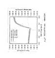
図5は、酸化亜鉛を活性層としてもつトップゲート構造トランジスタのVds−Idsカーブを示すグラフである。
図5では、上述のような製造工程によって、上記成膜条件にて第一ゲート絶縁膜5及び第二ゲート絶縁膜6を成膜して作製したトランジスタの動作特性(Vds−Idsカーブ)を示している。電界電子移動度μFE=14.3cm2/V・sec、しきい電界強度Vth=3.8Vの優れたトランジスタ特性であることがわかる。FIG. 5 is a graph showing a Vds-Ids curve of a top-gate transistor having zinc oxide as an active layer.
FIG. 5 shows operating characteristics (Vds-Ids curve) of a transistor manufactured by forming the first
以上のように、本発明に係る半導体装置は、その絶縁膜を、PE−CVD法においてTMSとN2Oとを用い、室温から250℃までの基板温度にて形成することによって、低温条件下でもN2OがTMSを効果的に酸化させ、熱酸化SiO薄膜と同等に炭素含有量を低く成膜することができるので、良好な膜質の絶縁膜を有する半導体装置となる。
また、絶縁膜を、ZnOを主成分とする酸化物半導体薄膜層上に形成する場合、酸化物半導体薄膜層の温度上昇を抑制することができるので、酸化物半導体薄膜層中に欠陥が生ずることなく、良好な絶縁膜を有する半導体装置を得ることが可能である。As described above, in the semiconductor device according to the present invention, the insulating film is formed at a substrate temperature from room temperature to 250 ° C. using TMS and N2 O in the PE-CVD method. However, since N2 O effectively oxidizes TMS and can form a film with a carbon content as low as that of a thermally oxidized SiO thin film, a semiconductor device having an insulating film with good film quality is obtained.
In addition, when the insulating film is formed over the oxide semiconductor thin film layer containing ZnO as a main component, a rise in temperature of the oxide semiconductor thin film layer can be suppressed, so that defects occur in the oxide semiconductor thin film layer. Thus, a semiconductor device having a good insulating film can be obtained.
また、半導体装置がTFTの場合、絶縁膜の直下に位置する半導体薄膜層の温度上昇を抑制することができるので、半導体薄膜層に欠陥が生ずることなく、半導体薄膜層の低抵抗化を防止することが可能となり、リーク電流の増大、電子移動度の低下を防ぐことが可能となる。また、良好な膜質の絶縁膜を有することによって、半導体薄膜層との界面特性が良好なものとなるので、さらにリーク電流が抑制された信頼性に優れたTFTを得ることが可能となる。 Further, when the semiconductor device is a TFT, the temperature rise of the semiconductor thin film layer located immediately below the insulating film can be suppressed, so that the resistance of the semiconductor thin film layer can be prevented from being lowered without causing defects in the semiconductor thin film layer. It becomes possible to prevent an increase in leakage current and a decrease in electron mobility. In addition, by having an insulating film having a good film quality, the interface characteristics with the semiconductor thin film layer are improved, and thus it is possible to obtain a TFT having excellent reliability in which leakage current is further suppressed.
本発明は、低温条件下で良質な絶縁膜を成膜する必要がある半導体装置に対して好適に利用されるものである。 The present invention is suitably used for a semiconductor device that needs to form a high-quality insulating film under a low temperature condition.
1 基板
2 一対のソース・ドレイン電極
3 低抵抗導電性薄膜
4 半導体薄膜層
5 第一ゲート絶縁膜
6 第二ゲート絶縁膜
7 ゲート電極DESCRIPTION OF
Claims (8)
Translated fromJapanese前記絶縁膜が、プラズマCVD法によって、絶縁膜の原料となるガスとしてTMSと、酸化ガスとして亜酸化窒素(N2O)とを用い、室温以上250℃以下の基板温度にて形成されることを特徴とする半導体装置の製法。In a method for manufacturing a semiconductor device having an insulating film formed under a low temperature condition using tetramethylsilane (TMS),
The insulating film is formed by a plasma CVD method using TMS as a source gas of the insulating film and nitrous oxide (N2 O) as an oxidizing gas at a substrate temperature of room temperature to 250 ° C. A process for producing a semiconductor device characterized by
Priority Applications (1)
| Application Number | Priority Date | Filing Date | Title |
|---|---|---|---|
| JP2006258080AJP5112668B2 (en) | 2006-09-22 | 2006-09-22 | Manufacturing method of semiconductor devices |
Applications Claiming Priority (1)
| Application Number | Priority Date | Filing Date | Title |
|---|---|---|---|
| JP2006258080AJP5112668B2 (en) | 2006-09-22 | 2006-09-22 | Manufacturing method of semiconductor devices |
Publications (2)
| Publication Number | Publication Date |
|---|---|
| JP2008078512Atrue JP2008078512A (en) | 2008-04-03 |
| JP5112668B2 JP5112668B2 (en) | 2013-01-09 |
Family
ID=39350242
Family Applications (1)
| Application Number | Title | Priority Date | Filing Date |
|---|---|---|---|
| JP2006258080AExpired - Fee RelatedJP5112668B2 (en) | 2006-09-22 | 2006-09-22 | Manufacturing method of semiconductor devices |
Country Status (1)
| Country | Link |
|---|---|
| JP (1) | JP5112668B2 (en) |
Cited By (2)
| Publication number | Priority date | Publication date | Assignee | Title |
|---|---|---|---|---|
| JP2011199264A (en)* | 2010-02-26 | 2011-10-06 | Semiconductor Energy Lab Co Ltd | Semiconductor device |
| JP2017017344A (en)* | 2010-01-22 | 2017-01-19 | 株式会社半導体エネルギー研究所 | Semiconductor device |
Citations (4)
| Publication number | Priority date | Publication date | Assignee | Title |
|---|---|---|---|---|
| JP2002299339A (en)* | 2000-09-01 | 2002-10-11 | Osamu Takai | Method for manufacturing silicon oxide film |
| JP2003037268A (en)* | 2001-07-24 | 2003-02-07 | Minolta Co Ltd | Semiconductor device and method of manufacturing the same |
| JP2004507103A (en)* | 2000-08-18 | 2004-03-04 | コーニンクレッカ フィリップス エレクトロニクス エヌ ヴィ | Method and structure for bonding MSQ material to liner oxide |
| JP5015534B2 (en)* | 2006-09-22 | 2012-08-29 | 財団法人高知県産業振興センター | Insulating film formation method |
- 2006
- 2006-09-22JPJP2006258080Apatent/JP5112668B2/ennot_activeExpired - Fee Related
Patent Citations (4)
| Publication number | Priority date | Publication date | Assignee | Title |
|---|---|---|---|---|
| JP2004507103A (en)* | 2000-08-18 | 2004-03-04 | コーニンクレッカ フィリップス エレクトロニクス エヌ ヴィ | Method and structure for bonding MSQ material to liner oxide |
| JP2002299339A (en)* | 2000-09-01 | 2002-10-11 | Osamu Takai | Method for manufacturing silicon oxide film |
| JP2003037268A (en)* | 2001-07-24 | 2003-02-07 | Minolta Co Ltd | Semiconductor device and method of manufacturing the same |
| JP5015534B2 (en)* | 2006-09-22 | 2012-08-29 | 財団法人高知県産業振興センター | Insulating film formation method |
Cited By (2)
| Publication number | Priority date | Publication date | Assignee | Title |
|---|---|---|---|---|
| JP2017017344A (en)* | 2010-01-22 | 2017-01-19 | 株式会社半導体エネルギー研究所 | Semiconductor device |
| JP2011199264A (en)* | 2010-02-26 | 2011-10-06 | Semiconductor Energy Lab Co Ltd | Semiconductor device |
Also Published As
| Publication number | Publication date |
|---|---|
| JP5112668B2 (en) | 2013-01-09 |
Similar Documents
| Publication | Publication Date | Title |
|---|---|---|
| JP5099740B2 (en) | Thin film transistor | |
| TWI514475B (en) | Method of forming a hydrogen-free germanium-containing dielectric layer | |
| JP5015471B2 (en) | Thin film transistor and manufacturing method thereof | |
| KR101670425B1 (en) | Capping layers for metal oxynitride tfts | |
| JP5584960B2 (en) | Thin film transistor and display device | |
| JP2007287890A (en) | Insulating film forming method, semiconductor device manufacturing method, plasma CVD apparatus | |
| JP2007287889A (en) | Insulating film forming method, semiconductor device manufacturing method | |
| TW201945570A (en) | High pressure annealing process for metal containing materials | |
| CN114303239B (en) | Nitrogen-rich silicon nitride films for thin-film transistors | |
| US20150380561A1 (en) | Metal oxide tft stability improvement | |
| JP5015534B2 (en) | Insulating film formation method | |
| CN102723359B (en) | Thin-film transistor, manufacture method of thin-film transistor, array substrate and display device | |
| US20070238254A1 (en) | Method of etching low dielectric constant films | |
| WO2021073193A1 (en) | Composite crystalline metal oxide thin film transistor having vertical structure and manufacturing method therefor | |
| JP5112668B2 (en) | Manufacturing method of semiconductor devices | |
| CN107369716B (en) | Thin film transistor, manufacturing method and display device | |
| US20090200553A1 (en) | High temperature thin film transistor on soda lime glass | |
| JP6703186B2 (en) | Thin film transistor and manufacturing method thereof | |
| US10748759B2 (en) | Methods for improved silicon nitride passivation films | |
| JP7640838B2 (en) | Method for forming silicon oxynitride film and method for manufacturing thin film transistor | |
| JP7696076B2 (en) | Method for manufacturing thin film transistor | |
| KR101970548B1 (en) | oxide including film, and oxide semiconductor thin film transistor, and fabrication method of oxide semiconductor thin film transistor using the same | |
| JP2025091771A (en) | Method for manufacturing thin film transistor | |
| US20090146264A1 (en) | Thin film transistor on soda lime glass with barrier layer |
Legal Events
| Date | Code | Title | Description |
|---|---|---|---|
| A621 | Written request for application examination | Free format text:JAPANESE INTERMEDIATE CODE: A621 Effective date:20090723 | |
| A977 | Report on retrieval | Free format text:JAPANESE INTERMEDIATE CODE: A971007 Effective date:20110708 | |
| A131 | Notification of reasons for refusal | Free format text:JAPANESE INTERMEDIATE CODE: A131 Effective date:20110808 | |
| A521 | Written amendment | Free format text:JAPANESE INTERMEDIATE CODE: A523 Effective date:20111006 | |
| A131 | Notification of reasons for refusal | Free format text:JAPANESE INTERMEDIATE CODE: A132 Effective date:20120709 | |
| A521 | Written amendment | Free format text:JAPANESE INTERMEDIATE CODE: A523 Effective date:20120830 | |
| A521 | Written amendment | Free format text:JAPANESE INTERMEDIATE CODE: A523 Effective date:20120906 | |
| TRDD | Decision of grant or rejection written | ||
| A01 | Written decision to grant a patent or to grant a registration (utility model) | Free format text:JAPANESE INTERMEDIATE CODE: A01 Effective date:20120924 | |
| A01 | Written decision to grant a patent or to grant a registration (utility model) | Free format text:JAPANESE INTERMEDIATE CODE: A01 | |
| A61 | First payment of annual fees (during grant procedure) | Free format text:JAPANESE INTERMEDIATE CODE: A61 Effective date:20121011 | |
| FPAY | Renewal fee payment (event date is renewal date of database) | Free format text:PAYMENT UNTIL: 20151019 Year of fee payment:3 | |
| R150 | Certificate of patent or registration of utility model | Free format text:JAPANESE INTERMEDIATE CODE: R150 | |
| LAPS | Cancellation because of no payment of annual fees |