JP2008065430A - Semiconductor device and IC card - Google Patents
Semiconductor device and IC cardDownload PDFInfo
- Publication number
- JP2008065430A JP2008065430AJP2006240011AJP2006240011AJP2008065430AJP 2008065430 AJP2008065430 AJP 2008065430AJP 2006240011 AJP2006240011 AJP 2006240011AJP 2006240011 AJP2006240011 AJP 2006240011AJP 2008065430 AJP2008065430 AJP 2008065430A
- Authority
- JP
- Japan
- Prior art keywords
- nonvolatile memory
- initial data
- initialization
- semiconductor device
- read
- Prior art date
- Legal status (The legal status is an assumption and is not a legal conclusion. Google has not performed a legal analysis and makes no representation as to the accuracy of the status listed.)
- Pending
Links
Images


Classifications
- G—PHYSICS
- G11—INFORMATION STORAGE
- G11C—STATIC STORES
- G11C7/00—Arrangements for writing information into, or reading information out from, a digital store
- G11C7/20—Memory cell initialisation circuits, e.g. when powering up or down, memory clear, latent image memory
- G—PHYSICS
- G11—INFORMATION STORAGE
- G11C—STATIC STORES
- G11C16/00—Erasable programmable read-only memories
- G11C16/02—Erasable programmable read-only memories electrically programmable
- G11C16/06—Auxiliary circuits, e.g. for writing into memory
- G11C16/10—Programming or data input circuits
- G11C16/20—Initialising; Data preset; Chip identification
- G—PHYSICS
- G11—INFORMATION STORAGE
- G11C—STATIC STORES
- G11C29/00—Checking stores for correct operation ; Subsequent repair; Testing stores during standby or offline operation
- G11C29/70—Masking faults in memories by using spares or by reconfiguring
- G11C29/72—Masking faults in memories by using spares or by reconfiguring with optimized replacement algorithms
Landscapes
- Storage Device Security (AREA)
- Memory System (AREA)
- Techniques For Improving Reliability Of Storages (AREA)
Abstract
Translated fromJapaneseDescription
Translated fromJapanese本発明は、不揮発性メモリを有する半導体装置、ICカードにかかわり、特に不揮発性メモリのデータ初期化を確実に行うための技術に関する。 The present invention relates to a semiconductor device and an IC card having a nonvolatile memory, and more particularly to a technique for surely initializing data in the nonvolatile memory.
不揮発性メモリは電源が供給されなくてもデータを保持できるため、多くのLSIに搭載されている。この場合、LSI製造者が必要な初期データを不揮発性メモリに格納した上で、LSIを出荷する。例えば、LSI製造時の製品管理情報や良品判定時の各種情報や機種固有情報等の各種データを初期データとして不揮発性メモリに記憶させておく。これは、出荷後の不良発生時におけるメンテナンス処理を容易にするためである(例えば特許文献1参照)。 Nonvolatile memories are stored in many LSIs because they can hold data even when power is not supplied. In this case, the LSI is shipped after the initial data required by the LSI manufacturer is stored in the nonvolatile memory. For example, various data such as product management information at the time of LSI manufacture, various information at the time of non-defective product determination, and model-specific information are stored in the nonvolatile memory as initial data. This is for facilitating maintenance processing when defects occur after shipment (see, for example, Patent Document 1).
また、ICカードに搭載されるLSIにおいては、LSIやICカードの輸送時の盗難などによる不正使用を防止するために、輸送鍵を使用する(例えば、特許文献2参照)。LSI製造時にこの輸送鍵の情報を初期データとして不揮発性メモリに格納した上で、LSIを出荷する。 In addition, in an LSI mounted on an IC card, a transport key is used in order to prevent unauthorized use due to theft or the like during transport of the LSI or IC card (see, for example, Patent Document 2). The LSI is shipped after the transport key information is stored in the nonvolatile memory as initial data when the LSI is manufactured.
上記の他にも、LSIの機能を設定するためのコンフィギュレーション情報等の初期データがLSI製造者により不揮発性メモリに格納される。
不揮発性メモリには強誘電体メモリやEEPROM、ヒューズメモリ、マスクROM等、様々な種類があり、それぞれに長所、短所がある。例えば、強誘電体メモリはアクセス速度が速く、書き換え回数が多いという長所がある反面、耐ストレス特性(耐熱ストレス特性や耐応力ストレス特性)は他の不揮発性メモリと比較すると劣るという短所がある。また例えば、ヒューズメモリは耐ストレス特性が高くデータ保持能力は優れている反面、1回しか書き換えができない。 There are various types of nonvolatile memory such as ferroelectric memory, EEPROM, fuse memory, mask ROM, etc., each having advantages and disadvantages. For example, a ferroelectric memory has advantages such as a high access speed and a large number of rewrites, but has a disadvantage that stress resistance characteristics (heat stress characteristics and stress stress characteristics) are inferior to those of other nonvolatile memories. Also, for example, the fuse memory has high stress resistance and excellent data retention capability, but can be rewritten only once.
LSIは、最終製品形態になるまでの工程において何らかのストレスが加えられることがある。例えば、基板実装時においては、LSIパッケージを基板にはんだ付けするためのリフロー工程で約250℃の熱ストレスが加えられる。しかし、不揮発性メモリとして強誘電体メモリを使用した場合には、工程中の熱ストレスにより初期データが破壊されることがある。一方、耐ストレス特性の高いヒューズメモリやEEPROMでは、アクセス速度や書き換え回数といった基本性能が要求仕様を満たせない。 LSI may be subjected to some stress in the process up to the final product form. For example, at the time of board mounting, thermal stress of about 250 ° C. is applied in a reflow process for soldering the LSI package to the board. However, when a ferroelectric memory is used as the nonvolatile memory, initial data may be destroyed due to thermal stress during the process. On the other hand, in a fuse memory or EEPROM having high stress resistance characteristics, basic performance such as access speed and the number of rewrites cannot satisfy the required specifications.
本発明は、このような事情に鑑みて創作したものであり、不揮発性メモリを搭載する半導体装置、ICカードにおいて、不揮発性メモリに要求される基本性能を低下させることなく、初期データを確実に保持させることができるようにすることを目的としている。 The present invention was created in view of such circumstances, and in a semiconductor device and IC card equipped with a non-volatile memory, the initial data is reliably obtained without degrading the basic performance required for the non-volatile memory. It is intended to be able to hold.
本発明による半導体装置は、
第1の不揮発性メモリと、
前記第1の不揮発性メモリよりも耐ストレス特性が高く初期データを格納している第2の不揮発性メモリと、
前記第2の不揮発性メモリから前記初期データを読み出し、読み出された前記初期データを前記第1の不揮発性メモリにコピーして初期化する初期化制御部とを備えたものである。A semiconductor device according to the present invention includes:
A first non-volatile memory;
A second nonvolatile memory having higher stress resistance than the first nonvolatile memory and storing initial data;
An initialization control unit that reads the initial data from the second nonvolatile memory, and copies and initializes the read initial data to the first nonvolatile memory.
この構成において、第2の不揮発性メモリは耐ストレス特性(耐熱ストレス特性/耐応力ストレス特性)が高い。初期の段階では、耐ストレス特性の高い第2の不揮発性メモリに初期データを格納しておく。そして、LSI出荷後において熱ストレスや応力ストレスが印加されたときでも、第2の不揮発性メモリに保持されている初期データは、第2の不揮発性メモリは耐ストレス特性が高いので、そのまま確実に保持される。熱ストレスや応力ストレスが印加された後においては、第2の不揮発性メモリから初期データを読み出して第1の不揮発性メモリにコピーする。第1の不揮発性メモリは耐ストレス特性は比較的低いものの、アクセス速度・書き換え回数等の性能に優れている。前記の熱ストレスや応力ストレスが印加されたときには、第1の不揮発性メモリには初期データがなく、熱ストレスや応力ストレスが印加されたのちに、第2の不揮発性メモリから第1の不揮発性メモリへ初期データがコピーされる。コピー後は、熱ストレスや応力ストレスの印加はないので、初期データは第1の不揮発性メモリにおいて確実に保持される。そして、第1の不揮発性メモリはアクセス速度・書き換え回数等の性能に優れている。したがって、全体として、不揮発性メモリの性能を損なうことなく、初期データを確実に保持することが可能となる。 In this configuration, the second nonvolatile memory has high stress resistance characteristics (heat resistance stress characteristics / stress stress characteristics). In the initial stage, initial data is stored in a second nonvolatile memory having high stress resistance characteristics. Even when thermal stress or stress stress is applied after LSI shipment, the initial data held in the second non-volatile memory can be reliably as-is because the second non-volatile memory has high stress resistance characteristics. Retained. After thermal stress or stress stress is applied, initial data is read from the second nonvolatile memory and copied to the first nonvolatile memory. Although the first nonvolatile memory has relatively low stress resistance characteristics, it has excellent performance such as access speed and number of rewrites. When the thermal stress or stress stress is applied, there is no initial data in the first nonvolatile memory, and after the thermal stress or stress stress is applied, the first nonvolatile memory starts with the first nonvolatile memory. Initial data is copied to memory. Since no thermal stress or stress stress is applied after copying, the initial data is reliably held in the first nonvolatile memory. The first nonvolatile memory is excellent in performance such as access speed and number of rewrites. Therefore, as a whole, initial data can be reliably held without impairing the performance of the nonvolatile memory.
上記構成の半導体装置において、前記初期化制御部は、前記第2の不揮発性メモリの所定のアドレスから前記初期データを読み出すリード部と、読み出された前記初期データを前記第1の不揮発性メモリの所定のアドレスに書き込むライト部を有しているものとする。 In the semiconductor device having the above configuration, the initialization control unit includes a read unit that reads the initial data from a predetermined address of the second nonvolatile memory, and the read initial data is the first nonvolatile memory. It is assumed that a write unit for writing to a predetermined address is provided.
また上記構成の半導体装置において、初期化の許可/禁止を示す初期化許可フラグを有し、前記初期データのコピーによる前記第1の不揮発性メモリの初期化が未了の状態では搭載機能の一部が無効化されかつ前記初期化許可フラグが許可状態とされ、前記初期化制御部は、前記初期データのコピーによる前記第1の不揮発性メモリの初期化完了に伴って前記初期化許可フラグを禁止状態へ移行させるという態様がある。 Further, the semiconductor device having the above-described configuration has an initialization permission flag indicating permission / prohibition of initialization, and when the initialization of the first nonvolatile memory by copying of the initial data has not been completed, one of the mounted functions. The initialization permission flag is set to a permitted state, and the initialization control unit sets the initialization permission flag when the initialization of the first non-volatile memory by copying the initial data is completed. There is a mode of shifting to the prohibited state.
この構成においては、第1の不揮発性メモリが初期化を経ていない状態では、半導体装置に搭載されている機能の一部が無効状態のままとなっている。機能の一部が無効状態のままであると、その機能が使えないので、第1の不揮発性メモリの初期化に向けての動機付けが働く。その機能を有効化するには、第1の不揮発性メモリの初期化が必須とされているからである。第1の不揮発性メモリの初期化をうながすのであるが、このときは初期化許可フラグは禁止状態ではなく許可状態であるので、第1の不揮発性メモリの初期化が可能である。すなわち、初期化制御部による第1の不揮発性メモリの初期化が完了するまでは初期化許可フラグを許可状態にしておき、機能の一部が無効状態となっていることを通じて、第1の不揮発性メモリの初期化をうながし、第1の不揮発性メモリの初期化を確実化することが可能となる。 In this configuration, in a state where the first nonvolatile memory has not been initialized, some of the functions mounted on the semiconductor device remain in an invalid state. If a part of the function remains in an invalid state, the function cannot be used, and motivation for the initialization of the first nonvolatile memory works. This is because the initialization of the first nonvolatile memory is indispensable in order to validate the function. Initialization of the first nonvolatile memory is prompted. At this time, since the initialization permission flag is not in the prohibited state but in the permitted state, the first nonvolatile memory can be initialized. That is, until the initialization of the first nonvolatile memory by the initialization control unit is completed, the initialization permission flag is set to a permitted state, and a part of the function is in an invalid state. Initialization of the non-volatile memory is prompted and initialization of the first nonvolatile memory can be ensured.
そして上記の構成において、前記初期化許可フラグが禁止状態へ移行された場合は、前記第2の不揮発性メモリの一部またはすべてのアドレスへのアクセスを禁止するという態様がある。 In the above configuration, when the initialization permission flag is shifted to a prohibited state, access to a part or all of the addresses of the second nonvolatile memory is prohibited.
この場合、アクセス禁止の第2の不揮発性メモリのアドレスにおいて、秘匿性の高い初期データを格納しておくものとする。初期化制御部により第1の不揮発性メモリを初期化した後は、秘匿性の高い初期データを格納している第2の不揮発性メモリのアドレスへのアクセスを禁止するので、秘匿性の高い初期データの暴露を防ぐことが可能となる。 In this case, initial data with high secrecy is stored at the address of the second nonvolatile memory whose access is prohibited. After initialization of the first nonvolatile memory by the initialization control unit, access to the address of the second nonvolatile memory storing the highly confidential initial data is prohibited. Data exposure can be prevented.
また上記構成の半導体装置において、前記第2の不揮発性メモリは、前記初期データに対して転送先アドレス情報を対にして格納しており、前記第2の不揮発性メモリから読み出された前記初期データは、前記転送先アドレス情報で指定された前記第1の不揮発性メモリのアドレスに転送格納されるという態様がある。 In the semiconductor device having the above configuration, the second non-volatile memory stores transfer address information paired with the initial data, and the initial data read from the second non-volatile memory is stored. There is a mode in which the data is transferred and stored at the address of the first nonvolatile memory specified by the transfer destination address information.
これによると、初期データの格納先アドレスを可変とすることが可能となるため、第1の不揮発性メモリの初期データのフォーマットが変更になった場合でも、容易に対応することが可能となる。 According to this, since the storage address of the initial data can be made variable, even when the format of the initial data of the first nonvolatile memory is changed, it is possible to easily cope with it.
また上記構成の半導体装置において、前記初期化制御部は、さらに、前記リード部によって前記第2の不揮発性メモリから読み出された前記初期データに対して演算処理を行い、その処理結果を前記ライト部に渡すデータ処理部を備えているという態様がある。 In the semiconductor device having the above-described configuration, the initialization control unit further performs arithmetic processing on the initial data read from the second nonvolatile memory by the read unit, and outputs the processing result to the write There is an aspect in which a data processing unit is provided to the unit.
これによると、第2の不揮発性メモリに格納しておく初期データを暗号化しておき、その暗号化された初期データをデータ処理部で復号化した上で第1の不揮発性メモリにコピーすれば、第2の不揮発性メモリにおいて初期データを暗号化状態でより安全に保持させることが可能となる。また、例えば輸送鍵のように輸送先にて照合した後、変更するような初期データについては、初期データの変更と格納を同時に行うことができるため、より効率的に第1の不揮発性メモリの初期化を行うことが可能である。 According to this, if the initial data stored in the second nonvolatile memory is encrypted, the encrypted initial data is decrypted by the data processing unit and then copied to the first nonvolatile memory. In the second nonvolatile memory, the initial data can be more securely held in the encrypted state. In addition, for example, initial data that is changed after being verified at the transport destination, such as a transport key, can be changed and stored at the same time, so that the first nonvolatile memory can be more efficiently stored. Initialization can be performed.
本発明によるICカードは、
上記のいずれかの半導体装置と、
リーダライタと通信を行う送受信回路と、
前記送受信回路が受信したコマンドに従って前記半導体装置における前記初期化制御部を制御して、前記第2の不揮発性メモリから前記初期データを読み出させ、読み出された前記初期データを前記第1の不揮発性メモリにコピーして書き込み初期化を行わせる制御回路とを備えたものである。The IC card according to the present invention is
Any one of the above semiconductor devices;
A transmission / reception circuit for communicating with a reader / writer;
The initialization control unit in the semiconductor device is controlled according to a command received by the transmission / reception circuit, the initial data is read from the second nonvolatile memory, and the read initial data is read from the first data And a control circuit that performs write initialization by copying to a nonvolatile memory.
これによると、不揮発性メモリを備えたICカードにおいて、ICカードの製造工程中において熱ストレスや応力ストレスが印加される工程までは、耐ストレス特性の高い第2の不揮発性メモリに初期データを格納しておき、ストレスが印加された後は、耐ストレス特性は比較的低いものの、アクセス速度・書き換え回数等の性能に優れた第1の不揮発性メモリに初期データをコピーすることで、不揮発性メモリの性能を損なうことなく、不揮発性メモリに格納される初期データを確実に保持することが可能となる。 According to this, in an IC card equipped with a non-volatile memory, initial data is stored in a second non-volatile memory having high stress resistance characteristics until a process in which thermal stress or stress stress is applied during the manufacturing process of the IC card. In addition, after the stress is applied, the non-volatile memory can be obtained by copying the initial data to the first non-volatile memory that has relatively low stress resistance characteristics but excellent performance such as access speed and number of rewrites. Thus, the initial data stored in the non-volatile memory can be reliably held without impairing the performance of the memory.
以上のように本発明によると、不揮発性メモリに要求される基本性能を損なうことなく、不揮発性メモリに格納される初期データを確実に保持することができる。 As described above, according to the present invention, the initial data stored in the nonvolatile memory can be reliably held without impairing the basic performance required for the nonvolatile memory.
以下、本発明にかかわる半導体装置、ICカードの実施の形態を図面を用いて詳細に説明する。 Embodiments of a semiconductor device and an IC card according to the present invention will be described below in detail with reference to the drawings.
(実施の形態1)
図1は本発明の実施の形態1における半導体装置Aの構成を示すブロック図である。半導体装置Aは、第1の不揮発性メモリ1、第2の不揮発性メモリ2、初期化制御部3、CPU4、読み出し専用メモリ5およびこれらを互いにつなぐバス6を備えている。(Embodiment 1)
FIG. 1 is a block diagram showing a configuration of a semiconductor device A according to the first embodiment of the present invention. The semiconductor device A includes a first
第1の不揮発性メモリ1は、例えばアクセス速度が速く、書き換え回数が多い強誘電体メモリである。これに対して、第2の不揮発性メモリ2は、例えば耐ストレス特性(耐熱ストレス特性/耐応力ストレス特性)が高いワンタイムライトメモリであるヒューズメモリである。初期データは、初期には耐ストレス特性が高い第2の不揮発性メモリ2に格納されている。初期には、第1の不揮発性メモリ1には初期データは格納されていない。第1の不揮発性メモリ1には、初期化の許可/禁止を示す初期化許可フラグが所定のアドレスに格納されている。初期化許可フラグは、所定のビットで表される値である。初期化許可フラグは、電源が切断された場合においても保持される。 The first
初期化制御部3は、リードアドレス発生部31、リード部32、ライトアドレス発生部33、ライト部34および初期化許可フラグ判定部35を備え、CPU4からの初期化信号INITを受けて第1の不揮発性メモリ1の初期化動作を開始するように構成されている。この初期化動作は、第2の不揮発性メモリ2から初期データを読み出して第1の不揮発性メモリ1へコピーすることである。リードアドレス発生部31は、第2の不揮発性メモリ2における初期データが格納されているアドレスを順次発生する。ライトアドレス発生部33は、初期データを第1の不揮発性メモリ1に格納するアドレスを順次発生する。リード部32は、リードアドレス発生部31が発生したアドレスにおいて第2の不揮発性メモリ2から初期データを読み出す。ライト部34は、読み出された初期データをライトアドレス発生部33が発生したアドレスにおいて第1の不揮発性メモリ1に書き込む。 The
初期化許可フラグ判定部35は、第1の不揮発性メモリ1から初期化許可フラグを読み出し、その初期化許可フラグが許可状態であるか禁止状態であるかを判定し、許可状態のときに初期化許可信号ENを生成してリード部32およびライト部34に出力する。初期化許可フラグの値があらかじめ決められた値と一致する場合に禁止状態にあると判定し、一致しない場合に許可状態にあると判定する。 The initialization permission
次に、上記のように構成された本実施の形態の半導体装置Aの動作を説明する。 Next, the operation of the semiconductor device A of the present embodiment configured as described above will be described.
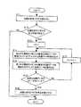
CPU4は、読み出し専用メモリ5に格納されているプログラムを実行するとともに、第1の不揮発性メモリ1および第2の不揮発性メモリ2に適宜アクセスする。また、CPU4は、実行プログラムに応じて初期化信号INITを出力する。初期化制御部3は、初期化信号INITを受けると、第1の不揮発性メモリ1の初期化動作を開始する。この初期化制御部3の動作を図2のフローチャートを用いて以下に説明する。前提として、この初期化動作のときまでに、熱ストレスや応力ストレスが印加されているとする。ただし、第1の不揮発性メモリ1の初期化は未了であるとする。電源が投入されCPU4から初期化信号INITを受けると、初期化制御部3はステップS11からの処理を開始する。 The CPU 4 executes a program stored in the read-
まず、ステップS11において、初期化制御部3のリード部32はバス6を介して第1の不揮発性メモリ1から初期化許可フラグを読み出し、初期化許可フラグ判定部35に渡す。 First, in step S <b> 11, the
次いでステップS12において、初期化許可フラグ判定部35は初期化許可フラグを判定する。禁止状態にあると判定した場合には、初期化動作を終了する。一方、許可状態にあると判定した場合には、初期化許可信号ENを生成してリード部32およびライト部34に出力し、ステップS13に進む。 Next, in step S12, the initialization permission
ステップS13において、何番目の初期データのコピーを行うかを示す変数Nを初期値の1に設定する。 In step S13, a variable N indicating what number of initial data is to be copied is set to an initial value of 1.
次いでステップS14において、リードアドレス発生部31は第2の不揮発性メモリ2においてN番目の初期データが格納されているアドレスを発生し、そのリードアドレスにおいてリード部32は第2の不揮発性メモリ2から初期データを読み出す。 Next, in step S <b> 14, the read
次いでステップS15において、ライトアドレス発生部33は第1の不揮発性メモリ1においてN番目の初期データを格納するアドレスを発生し、そのライトアドレスにおいてライト部34はステップS14で読み出した初期データを第1の不揮発性メモリ1に書き込む。 Next, in step S15, the write
次いでステップS16において、必要な初期データのコピーが完了したかを判定し、完了していないときはステップS17に進み、完了したときはステップS18に進む。 Next, in step S16, it is determined whether copying of necessary initial data has been completed. If it has not been completed, the process proceeds to step S17, and if it has been completed, the process proceeds to step S18.
必要な初期データのコピーが完了していないときにステップS17に進むと、変数Nをインクリメント(+1)し、ステップS14に戻る。必要な初期データのコピーが完了するまで、変数Nをインクリメントしながら、ステップS14〜S17を繰り返す。 If the process proceeds to step S17 when copying of necessary initial data is not completed, the variable N is incremented (+1), and the process returns to step S14. Steps S14 to S17 are repeated while incrementing the variable N until the necessary initial data copy is completed.
必要な初期データのコピーを完了してステップS18に進むと、初期化許可フラグの状態を禁止状態に変更し、初期化動作を終了する。 When the necessary initial data copy is completed and the process proceeds to step S18, the state of the initialization permission flag is changed to the prohibited state, and the initialization operation is terminated.
以上のように本実施の形態によれば、ストレスがかかる工程までは、書き換え回数は少ないが耐ストレス性の高い第2の不揮発性メモリ2に初期データを格納しておき、ストレスが印加された後は、耐ストレス特性は比較的低いものの、アクセス速度が速く書き換え回数の多い第1の不揮発性メモリ1に初期データをコピーすることで、不揮発性メモリに要求される基本性能を満足しつつ、初期データを確実に保持することが可能となる。 As described above, according to the present embodiment, the initial data is stored in the second
本実施の形態の変形の態様として、次のように構成してもよい。 As a modification of the present embodiment, the following configuration may be adopted.
(1)初期データのコピーによる第1の不揮発性メモリ1の初期化が未了の状態では、搭載機能の一部が無効化されかつ初期化許可フラグが許可状態とされているものとする。搭載機能の一部を無効化については、具体的には、読み出し専用メモリ5のアクセス可能な領域を限定することで、読み出し専用メモリ5に格納されているライブラリ関数やデバイスドライバの使用を禁止する。機能の一部が無効状態のままであると、その機能が使えないので、第1の不揮発性メモリ1を初期化するように動機付けが働く。読み出し専用メモリ5に格納されているライブラリ関数やデバイスドライバを有効にするためには、第1の不揮発性メモリ1の初期化を行うことが必須となる。これにより、第1の不揮発性メモリ1の初期化をうながすのであるが、このときは初期化許可フラグは禁止状態ではなく許可状態であるので、第1の不揮発性メモリ1の初期化が可能である。すなわち、初期化制御部3による第1の不揮発性メモリ1の初期化が完了するまでは初期化許可フラグを許可状態にしておき、機能の一部が無効状態となっていることを通じて、第1の不揮発性メモリ1の初期化をうながし、第1の不揮発性メモリ1の初期化を確実化することが可能となる。なお、第1の不揮発性メモリ1の初期化完了に伴って初期化許可フラグは禁止状態へ移行される。 (1) In the state where the initialization of the first
(2)第2の不揮発性メモリ2において、秘匿性の高い初期データを格納しておくものとする。第1の不揮発性メモリ1の初期化完了に伴って初期化許可フラグが禁止状態へ移行された場合は、秘匿性の高い初期データを格納している第2の不揮発性メモリ2の一部またはすべてのアドレスへのアクセスを禁止する。これにより、秘匿性の高い初期データが暴露される可能性を低減することが可能となる。 (2) It is assumed that the second
(実施の形態2)
図3は本発明の実施の形態2における半導体装置での第2の不揮発性メモリ2に格納する初期データのフォーマットを示す。このフォーマットは、初期データと、その初期データを格納するアドレス情報とを対にしている。そして、本実施の形態の半導体装置Aは、第2の不揮発性メモリ2に格納されているアドレス情報に基づいて第1の不揮発性メモリ1における初期データの格納先を決定するように構成されている。本実施の形態の半導体装置Aの構成は、実施の形態1の場合の図1の構成と同じである。(Embodiment 2)
FIG. 3 shows a format of initial data stored in the second
図4は、図3に示す初期データのフォーマットに基づいて初期データのコピーを行う場合のフローチャートである。図2に示すフローチャートと異なる点は、ステップS14,S15の代わりに、それぞれステップS14a,S15aを有することである。同じ点は説明を省略して異なる点を中心に説明する。 FIG. 4 is a flowchart for copying initial data based on the initial data format shown in FIG. The difference from the flowchart shown in FIG. 2 is that steps S14a and S15a are provided instead of steps S14 and S15, respectively. Explanation of the same points will be omitted, focusing on different points.
ステップS14aにおいては、リード部32は、リードアドレス発生部31によるリードアドレスで第2の不揮発性メモリ2をアクセスし、初期データとともにその初期データの格納先アドレスを読み出す。 In step S14a, the
次いでステップS15aにおいて、ライト部34は、ステップS14aで読み出された第1の不揮発性メモリ1の格納先アドレスにステップS14aで読み出された初期データを書き込む。この場合、ライトアドレス発生部33は機能を停止する。 Next, in step S15a, the
本実施の形態によれば、第1の不揮発性メモリ1における初期データの格納先を可変にできるため、第1の不揮発性メモリ1の初期データのフォーマットが変更になった場合でも、容易に対応することが可能となる。 According to the present embodiment, since the storage location of the initial data in the first
(実施の形態3)
図5は本発明の実施の形態3における半導体装置Aの構成を示すブロック図である。図5において、実施の形態1の図1におけるのと同じ符号は同一構成要素を指している。本実施の形態に特有の構成は、次のとおりである。第2の不揮発性メモリ2には、暗号化された状態の初期データが格納されているものとする。初期化制御部3において、データ処理部36が追加されている。このデータ処理部36には、リード部32によって第2の不揮発性メモリ2から読み出された初期データに対し所定の演算処理(論理演算、数値演算)を行い、その処理の結果をライト部34に渡すように構成されている。ライト部34は、データ処理部36によって演算処理された結果としてのデータを第1の不揮発性メモリ1に書き込む。その他の構成については、実施の形態1と同様であるので、説明を省略する。(Embodiment 3)
FIG. 5 is a block diagram showing a configuration of the semiconductor device A according to the third embodiment of the present invention. In FIG. 5, the same reference numerals as in FIG. 1 of the first embodiment indicate the same components. The configuration specific to the present embodiment is as follows. The second
次に、上記のように構成された本実施の形態の半導体装置Aの動作を説明する。 Next, the operation of the semiconductor device A of the present embodiment configured as described above will be described.
第2の不揮発性メモリ2に格納されている初期データをそのまま第1の不揮発性メモリ1にコピーする代わりに、読み出された初期データに対し所定のデータ処理を行った結果としてのデータを第1の不揮発性メモリ1の初期データとして格納する。例えば、第2の不揮発性メモリ2に格納されている暗号化された初期データは、データ処理部36により復号化した上で第1の不揮発性メモリ1に格納する。第2の不揮発性メモリ2に格納しておく初期データを暗号化しておくことで、初期データをより安全な状態で保持させることが可能となる。また、例えば輸送鍵のように輸送先にて照合した後、変更するような初期データについては、初期データの変更と格納を同時に行うことができるため、より効率的に第1の不揮発性メモリの初期化を行うことが可能である。なお、データ処理部36は、特定の初期データについてのみデータ処理を行うようにしてもよい。 Instead of copying the initial data stored in the second
(実施の形態4)
図6は本発明の実施の形態4におけるICカードBの構成を示すブロック図である。ICカードBは、第1の不揮発性メモリ1、第2の不揮発性メモリ2、初期化制御部3、バス6、送受信回路7および制御回路8を備えている。なお、第1の不揮発性メモリ1、第2の不揮発性メモリ2および初期化制御部3は上述したとおりである。(Embodiment 4)
FIG. 6 is a block diagram showing the configuration of the IC card B according to Embodiment 4 of the present invention. The IC card B includes a first
送受信回路7は、無線または有線通信により、図示しないリーダライタからコマンドを受信し、また、リーダライタに対してレスポンスを送信するものとして構成されている。制御回路8は、送受信回路7が受信したコマンドに従って適宜、第1の不揮発性メモリ1にアクセスしてデータの読み書きを行い、読み出したデータを適宜、送受信回路7に送るように構成されている。また、制御回路8は、リーダライタから受信したコマンドがカードテストコマンドである場合に、初期化信号INITを生成して初期化制御部3に出力する。また、制御回路8は、初期化許可フラグ判定部35において初期化許可フラグが許可状態にあると判定されている状態においては、カードテストコマンド以外のコマンド(例えばライトコマンドやリードコマンド)に対しては処理を行わず、さらに、初期化許可フラグが禁止状態にあると判定されている状態においては、カードテストコマンドに対しては処理を行わないように構成されている。その他の構成については、実施の形態1の場合の図1と同様であるので、同一の構成要素について同一の参照符号を付すにとどめ、詳しい説明は省略する。 The transmission / reception circuit 7 is configured to receive a command from a reader / writer (not shown) by wireless or wired communication and to transmit a response to the reader / writer. The control circuit 8 is configured to access the first
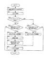
次に、図7のフローチャートを参照しながら、ICカードBの動作について説明する。 Next, the operation of the IC card B will be described with reference to the flowchart of FIG.
まず、電源が投入されると、ステップS21において、初期化制御部3のリード部32はバス6を介して第1の不揮発性メモリ1から初期化許可フラグを読み出し、初期化許可フラグ判定部35に渡す。 First, when the power is turned on, in step S21, the
次いでステップS22において、リーダライタから出力されたコマンドを送受信回路7によって受信する。 In step S22, the transmission / reception circuit 7 receives the command output from the reader / writer.
次いでステップS23において、制御回路8は、受信したコマンドがカードテストコマンドであるか否かを判定する。カードテストコマンドの場合はステップS24に進み、カードテストコマンドでない場合はステップS28に進む。 Next, in step S23, the control circuit 8 determines whether or not the received command is a card test command. If it is a card test command, the process proceeds to step S24, and if it is not a card test command, the process proceeds to step S28.
ステップS24に進むと、初期化許可フラグ判定部35は初期化許可フラグを判定する。禁止状態にあると判定した場合には、初期化動作を終了する。一方、許可状態にあると判定した場合には、ステップS25に進む。 In step S24, the initialization permission
ステップS25において、コマンドに従った処理を実行する。 In step S25, processing according to the command is executed.
次いでステップS26において、初期化制御部3は、第1の不揮発性メモリ1の初期化処理を実行する。この初期化処理の具体的内容は実施の形態1の場合と同様である。 Next, in step S <b> 26, the
初期化処理の完了後、ステップS27において、初期化許可フラグを禁止状態にする。 After the initialization process is completed, the initialization permission flag is set to a prohibited state in step S27.
次いでステップS30において、送受信回路7からリーダライタへレスポンスを送信する。なお、ステップS24で初期化許可フラグが禁止状態であるときには、レスポンス送信を行うことなく処理を終了する。 Next, in step S30, a response is transmitted from the transmission / reception circuit 7 to the reader / writer. Note that when the initialization permission flag is in the prohibited state in step S24, the process is terminated without performing response transmission.
受信したコマンドがカードテストコマンド以外の場合でステップS28に進んだときには、初期化許可フラグが禁止状態であるか否かを判断する。そして、禁止状態になっているときにはステップS29に進んで、コマンドに従った処理を実行し、レスポンス送信のステップS30に進む。一方、ステップS28において、初期化許可フラグが許可状態であるときには、レスポンス送信を行うことなく処理を終了する。 When the received command is other than the card test command and the process proceeds to step S28, it is determined whether or not the initialization permission flag is in a prohibited state. When it is in the prohibited state, the process proceeds to step S29, the process according to the command is executed, and the process proceeds to step S30 for response transmission. On the other hand, if the initialization permission flag is in the permitted state in step S28, the process ends without performing response transmission.
以上のように本実施の形態によれば、不揮発性メモリを備えたICカードBにおいて、送受信回路7が受信したコマンドに従って第1の不揮発性メモリ1の初期化を実行するもので、カードテストと連動させての第1の不揮発性メモリ1の初期化が可能である。また、ストレスがかかる工程までは、書き換え回数は少ないが耐ストレス性の高い第2の不揮発性メモリ2に初期データを格納しておき、ストレスが印加された後は、耐ストレス特性は比較的低いものの、アクセス速度が速く書き換え回数の多い第1の不揮発性メモリ1に初期データをコピーすることで、不揮発性メモリに要求される基本性能を満足しつつ、初期データを確実に保持することが可能となる。 As described above, according to the present embodiment, in the IC card B provided with the nonvolatile memory, the initialization of the first
また、第1の不揮発性メモリ1が初期化されていない状態で、通常のコマンドを処理することがなくなるため、ICカードBをより安全に運用することができる。 In addition, since the normal command is not processed when the first
なお、上記のいずれの実施の形態においても、初期化制御部3をCPU4内のソフトウェア処理として構成してもよい。この場合、ハードウェアとしての初期化制御部3は必要でなくなる。 In any of the above embodiments, the
本発明における半導体装置は、耐ストレス性が比較的低い不揮発性メモリにおいても、確実に初期データの保持が可能であるため、特に、LSI出荷時に初期データの格納が必要であり、かつ、最終製品形態に至るまでの工程において熱ストレスや応力ストレス等が印加される可能性のある半導体装置において有用である。 Since the semiconductor device according to the present invention can reliably retain initial data even in a non-volatile memory having relatively low stress resistance, it is necessary to store initial data especially at the time of LSI shipment, and the final product. This is useful in a semiconductor device in which thermal stress, stress stress, or the like may be applied in the process up to the form.
A 半導体装置
B ICカード
1 第1の不揮発性メモリ(強誘電体メモリ)
2 第2の不揮発性メモリ(ヒューズメモリ)
3 初期化制御部
4 CPU
5 読み出し専用メモリ
6 バス
7 送受信回路
8 制御回路
31 リードアドレス発生部
32 リード部
33 ライトアドレス発生部
34 ライト部
35 初期化許可フラグ判定部
36 データ処理部A Semiconductor device
2 Second non-volatile memory (fuse memory)
3 Initialization control unit 4 CPU
DESCRIPTION OF
Claims (7)
Translated fromJapanese前記第1の不揮発性メモリよりも耐ストレス特性が高く初期データを格納している第2の不揮発性メモリと、
前記第2の不揮発性メモリから前記初期データを読み出し、読み出された前記初期データを前記第1の不揮発性メモリにコピーして初期化する初期化制御部とを備えた半導体装置。A first non-volatile memory;
A second nonvolatile memory having higher stress resistance than the first nonvolatile memory and storing initial data;
A semiconductor device comprising: an initialization control unit that reads the initial data from the second nonvolatile memory, and copies and initializes the read initial data to the first nonvolatile memory.
リーダライタと通信を行う送受信回路と、
前記送受信回路が受信したコマンドに従って前記半導体装置における前記初期化制御部を制御して、前記第2の不揮発性メモリから前記初期データを読み出させ、読み出された前記初期データを前記第1の不揮発性メモリにコピーして書き込み初期化を行わせる制御回路とを備えたICカード。A semiconductor device according to any one of claims 1 to 6,
A transmission / reception circuit for communicating with a reader / writer;
The initialization control unit in the semiconductor device is controlled according to a command received by the transmission / reception circuit, the initial data is read from the second nonvolatile memory, and the read initial data is read from the first data An IC card provided with a control circuit for copying to a nonvolatile memory and performing writing initialization.
Priority Applications (3)
| Application Number | Priority Date | Filing Date | Title |
|---|---|---|---|
| JP2006240011AJP2008065430A (en) | 2006-09-05 | 2006-09-05 | Semiconductor device and IC card |
| CNA2007101495088ACN101140546A (en) | 2006-09-05 | 2007-09-04 | Semiconductor devices and IC cards |
| US11/896,668US7711917B2 (en) | 2006-09-05 | 2007-09-05 | Semiconductor device and IC card |
Applications Claiming Priority (1)
| Application Number | Priority Date | Filing Date | Title |
|---|---|---|---|
| JP2006240011AJP2008065430A (en) | 2006-09-05 | 2006-09-05 | Semiconductor device and IC card |
Publications (1)
| Publication Number | Publication Date |
|---|---|
| JP2008065430Atrue JP2008065430A (en) | 2008-03-21 |
Family
ID=39153392
Family Applications (1)
| Application Number | Title | Priority Date | Filing Date |
|---|---|---|---|
| JP2006240011APendingJP2008065430A (en) | 2006-09-05 | 2006-09-05 | Semiconductor device and IC card |
Country Status (3)
| Country | Link |
|---|---|
| US (1) | US7711917B2 (en) |
| JP (1) | JP2008065430A (en) |
| CN (1) | CN101140546A (en) |
Cited By (1)
| Publication number | Priority date | Publication date | Assignee | Title |
|---|---|---|---|---|
| JP7538085B2 (en) | 2021-05-27 | 2024-08-21 | ルネサスエレクトロニクス株式会社 | Semiconductor Device |
Families Citing this family (8)
| Publication number | Priority date | Publication date | Assignee | Title |
|---|---|---|---|---|
| TWI387023B (en)* | 2008-12-25 | 2013-02-21 | Silicon Motion Inc | Method of preventing data loss during a solder reflow process and memory device using the same |
| CN102576330B (en)* | 2009-06-12 | 2015-01-28 | 提琴存储器公司 | Storage system with persistent garbage collection mechanism |
| KR102039537B1 (en) | 2013-03-15 | 2019-11-01 | 삼성전자주식회사 | Nonvolatile storage device and os image program method thereof |
| CN105094689B (en)* | 2014-05-16 | 2018-06-15 | 华为技术有限公司 | Nonvolatile memory NVM page frames initial method, device and system |
| US10168901B2 (en)* | 2015-03-12 | 2019-01-01 | Toshiba Memory Corporation | Memory system, information processing apparatus, control method, and initialization apparatus |
| JP6556489B2 (en)* | 2015-04-30 | 2019-08-07 | 株式会社東芝 | IC card, IC module, issuing device, issuing method, and issuing program |
| US9704595B1 (en) | 2016-03-31 | 2017-07-11 | Sandisk Technologies Llc | Self-detecting a heating event to non-volatile storage |
| CN113451309B (en) | 2020-03-25 | 2025-01-14 | 长鑫存储技术有限公司 | Semiconductor structure and preheating method thereof |
Citations (5)
| Publication number | Priority date | Publication date | Assignee | Title |
|---|---|---|---|---|
| JPH11250204A (en)* | 1998-02-27 | 1999-09-17 | Dainippon Printing Co Ltd | IC card |
| JP2001209766A (en)* | 2000-01-26 | 2001-08-03 | Nec Microcomputer Technology Ltd | Memory initialization system for ic card |
| JP2003323597A (en)* | 2002-02-28 | 2003-11-14 | Matsushita Electric Ind Co Ltd | Memory card |
| JP2004272400A (en)* | 2003-03-06 | 2004-09-30 | Renesas Technology Corp | Memory card |
| JP2005148808A (en)* | 2003-11-11 | 2005-06-09 | Matsushita Electric Ind Co Ltd | IC card and IC card initialization method |
Family Cites Families (4)
| Publication number | Priority date | Publication date | Assignee | Title |
|---|---|---|---|---|
| TW358939B (en)* | 1997-07-03 | 1999-05-21 | United Microelectronics Corp | Reparable memory module and method of repairing the memory module |
| JP2000259602A (en) | 1999-03-09 | 2000-09-22 | Sanyo Electric Co Ltd | One chip micro computer and its data managing method |
| JP3916862B2 (en) | 2000-10-03 | 2007-05-23 | 株式会社東芝 | Nonvolatile semiconductor memory device |
| JP2004102635A (en) | 2002-09-09 | 2004-04-02 | Ricoh Co Ltd | User authentication method, information system, document storage device, and digital multifunction peripheral |
- 2006
- 2006-09-05JPJP2006240011Apatent/JP2008065430A/enactivePending
- 2007
- 2007-09-04CNCNA2007101495088Apatent/CN101140546A/enactivePending
- 2007-09-05USUS11/896,668patent/US7711917B2/ennot_activeExpired - Fee Related
Patent Citations (5)
| Publication number | Priority date | Publication date | Assignee | Title |
|---|---|---|---|---|
| JPH11250204A (en)* | 1998-02-27 | 1999-09-17 | Dainippon Printing Co Ltd | IC card |
| JP2001209766A (en)* | 2000-01-26 | 2001-08-03 | Nec Microcomputer Technology Ltd | Memory initialization system for ic card |
| JP2003323597A (en)* | 2002-02-28 | 2003-11-14 | Matsushita Electric Ind Co Ltd | Memory card |
| JP2004272400A (en)* | 2003-03-06 | 2004-09-30 | Renesas Technology Corp | Memory card |
| JP2005148808A (en)* | 2003-11-11 | 2005-06-09 | Matsushita Electric Ind Co Ltd | IC card and IC card initialization method |
Cited By (1)
| Publication number | Priority date | Publication date | Assignee | Title |
|---|---|---|---|---|
| JP7538085B2 (en) | 2021-05-27 | 2024-08-21 | ルネサスエレクトロニクス株式会社 | Semiconductor Device |
Also Published As
| Publication number | Publication date |
|---|---|
| CN101140546A (en) | 2008-03-12 |
| US20080059703A1 (en) | 2008-03-06 |
| US7711917B2 (en) | 2010-05-04 |
Similar Documents
| Publication | Publication Date | Title |
|---|---|---|
| JP2008065430A (en) | Semiconductor device and IC card | |
| US7461268B2 (en) | E-fuses for storing security version data | |
| CN110034932B (en) | Communication system and operation method thereof | |
| JP5114617B2 (en) | Secure terminal, program, and method for protecting private key | |
| JP3638770B2 (en) | Storage device with test function | |
| US7076667B1 (en) | Storage device having secure test process | |
| JP2001356963A (en) | Semiconductor device and control device therefor | |
| JP3898481B2 (en) | Semiconductor memory device | |
| CN100428187C (en) | non-volatile memory device | |
| CN112068904A (en) | Chip boot operation method, device and related assembly | |
| US11372558B2 (en) | Method for accessing one-time-programmable memory and associated circuitry | |
| JP2008123106A (en) | Microcomputer and debug method for microcomputer | |
| JP4256859B2 (en) | Semiconductor memory device | |
| JP2012155363A (en) | Semiconductor device | |
| JP4591163B2 (en) | Bus access control device | |
| US8397081B2 (en) | Device and method for securing software | |
| US7916549B2 (en) | Memory self-test circuit, semiconductor device and IC card including the same, and memory self-test method | |
| JP5798007B2 (en) | Microcomputer and data processing apparatus | |
| CN114510753A (en) | Memory data protection method and device, electronic equipment and storage medium | |
| JP2011150495A (en) | Storage device | |
| JP5494389B2 (en) | Electronic control unit | |
| JP4447059B2 (en) | IC card and IC card inspection method | |
| JP6958962B2 (en) | Semiconductor memory devices and semiconductor memory systems | |
| CN116383900A (en) | Data processing apparatus and data processing method | |
| JP2007064762A (en) | Semiconductor device, test mode control circuit |
Legal Events
| Date | Code | Title | Description |
|---|---|---|---|
| A621 | Written request for application examination | Free format text:JAPANESE INTERMEDIATE CODE: A621 Effective date:20090526 | |
| A977 | Report on retrieval | Free format text:JAPANESE INTERMEDIATE CODE: A971007 Effective date:20120208 | |
| A131 | Notification of reasons for refusal | Free format text:JAPANESE INTERMEDIATE CODE: A131 Effective date:20120214 | |
| A02 | Decision of refusal | Free format text:JAPANESE INTERMEDIATE CODE: A02 Effective date:20120703 |