JP2008061109A - Electronic equipment and electrical circuits - Google Patents
Electronic equipment and electrical circuitsDownload PDFInfo
- Publication number
- JP2008061109A JP2008061109AJP2006237956AJP2006237956AJP2008061109AJP 2008061109 AJP2008061109 AJP 2008061109AJP 2006237956 AJP2006237956 AJP 2006237956AJP 2006237956 AJP2006237956 AJP 2006237956AJP 2008061109 AJP2008061109 AJP 2008061109A
- Authority
- JP
- Japan
- Prior art keywords
- antenna element
- wiring board
- printed wiring
- component
- housing
- Prior art date
- Legal status (The legal status is an assumption and is not a legal conclusion. Google has not performed a legal analysis and makes no representation as to the accuracy of the status listed.)
- Pending
Links
Images


Classifications
- H—ELECTRICITY
- H01—ELECTRIC ELEMENTS
- H01Q—ANTENNAS, i.e. RADIO AERIALS
- H01Q1/00—Details of, or arrangements associated with, antennas
- H01Q1/12—Supports; Mounting means
- H01Q1/22—Supports; Mounting means by structural association with other equipment or articles
- H01Q1/24—Supports; Mounting means by structural association with other equipment or articles with receiving set
- H01Q1/241—Supports; Mounting means by structural association with other equipment or articles with receiving set used in mobile communications, e.g. GSM
- H01Q1/242—Supports; Mounting means by structural association with other equipment or articles with receiving set used in mobile communications, e.g. GSM specially adapted for hand-held use
- H01Q1/243—Supports; Mounting means by structural association with other equipment or articles with receiving set used in mobile communications, e.g. GSM specially adapted for hand-held use with built-in antennas
- H—ELECTRICITY
- H01—ELECTRIC ELEMENTS
- H01Q—ANTENNAS, i.e. RADIO AERIALS
- H01Q9/00—Electrically-short antennas having dimensions not more than twice the operating wavelength and consisting of conductive active radiating elements
- H01Q9/04—Resonant antennas
- H01Q9/30—Resonant antennas with feed to end of elongated active element, e.g. unipole
- H—ELECTRICITY
- H05—ELECTRIC TECHNIQUES NOT OTHERWISE PROVIDED FOR
- H05K—PRINTED CIRCUITS; CASINGS OR CONSTRUCTIONAL DETAILS OF ELECTRIC APPARATUS; MANUFACTURE OF ASSEMBLAGES OF ELECTRICAL COMPONENTS
- H05K1/00—Printed circuits
- H05K1/18—Printed circuits structurally associated with non-printed electric components
- H05K1/181—Printed circuits structurally associated with non-printed electric components associated with surface mounted components
- H—ELECTRICITY
- H05—ELECTRIC TECHNIQUES NOT OTHERWISE PROVIDED FOR
- H05K—PRINTED CIRCUITS; CASINGS OR CONSTRUCTIONAL DETAILS OF ELECTRIC APPARATUS; MANUFACTURE OF ASSEMBLAGES OF ELECTRICAL COMPONENTS
- H05K2201/00—Indexing scheme relating to printed circuits covered by H05K1/00
- H05K2201/10—Details of components or other objects attached to or integrated in a printed circuit board
- H05K2201/10007—Types of components
- H05K2201/10128—Display
- H05K2201/10136—Liquid Crystal display [LCD]
- H—ELECTRICITY
- H05—ELECTRIC TECHNIQUES NOT OTHERWISE PROVIDED FOR
- H05K—PRINTED CIRCUITS; CASINGS OR CONSTRUCTIONAL DETAILS OF ELECTRIC APPARATUS; MANUFACTURE OF ASSEMBLAGES OF ELECTRICAL COMPONENTS
- H05K2203/00—Indexing scheme relating to apparatus or processes for manufacturing printed circuits covered by H05K3/00
- H05K2203/15—Position of the PCB during processing
- H05K2203/1572—Processing both sides of a PCB by the same process; Providing a similar arrangement of components on both sides; Making interlayer connections from two sides
- Y—GENERAL TAGGING OF NEW TECHNOLOGICAL DEVELOPMENTS; GENERAL TAGGING OF CROSS-SECTIONAL TECHNOLOGIES SPANNING OVER SEVERAL SECTIONS OF THE IPC; TECHNICAL SUBJECTS COVERED BY FORMER USPC CROSS-REFERENCE ART COLLECTIONS [XRACs] AND DIGESTS
- Y02—TECHNOLOGIES OR APPLICATIONS FOR MITIGATION OR ADAPTATION AGAINST CLIMATE CHANGE
- Y02P—CLIMATE CHANGE MITIGATION TECHNOLOGIES IN THE PRODUCTION OR PROCESSING OF GOODS
- Y02P70/00—Climate change mitigation technologies in the production process for final industrial or consumer products
- Y02P70/50—Manufacturing or production processes characterised by the final manufactured product
Landscapes
- Engineering & Computer Science (AREA)
- Computer Networks & Wireless Communication (AREA)
- Microelectronics & Electronic Packaging (AREA)
- Support Of Aerials (AREA)
- Details Of Aerials (AREA)
- Transceivers (AREA)
Abstract
Translated fromJapaneseDescription
Translated fromJapanese本発明は、記憶機構を内蔵した電子機器およびこれに実装される電気回路に関する。 The present invention relates to an electronic device having a built-in storage mechanism and an electric circuit mounted thereon.
例えば、記憶機構を内蔵した電子機器として、次のようなものがある。この電子機器は、筐体と、筐体の内部に収容されるプリント配線板と、ハードディスクと、バッテリと、ディスプレイと、プリント配線板に実装されるアンテナ素子と、を備えている。アンテナ素子は、筐体の厚み方向における中間部に配置している。電子機器は、このアンテナ素子により、通信相手となる他の電子機器との間で無線通信を行うことができる。 For example, there are the following electronic devices with a built-in storage mechanism. This electronic device includes a housing, a printed wiring board housed in the housing, a hard disk, a battery, a display, and an antenna element mounted on the printed wiring board. The antenna element is disposed at an intermediate portion in the thickness direction of the housing. The electronic device can perform wireless communication with another electronic device that is a communication partner by using the antenna element.
このような電子機器を机の上側に横置きすると、机によって無線電波が遮られることがある。このため、上記従来例では、アンテナ素子を筐体の厚み方向における中間部に配置することで、アンテナ素子と机との間に隙間を確保している。これにより、アンテナ素子から発信される電波が机によって遮断されるのを防いで、無線通信を安定化している(例えば、特許文献1参照)。
しかし、電子機器の無線通信に悪影響を及ぼすものとしては、机の他にも種々存在する。上記従来の電子機器では、このような悪影響を及ぼすものに対して対応することができず、改良の余地があった。 However, there are various types other than desks that adversely affect wireless communication of electronic devices. The above-described conventional electronic devices cannot cope with such adverse effects and have room for improvement.
本発明の目的は、アンテナ素子による無線通信に悪影響を及ぼす要因を排除して、安定的に無線通信を行うことができる電子機器を提供することにある。 An object of the present invention is to provide an electronic apparatus that can stably perform wireless communication by eliminating factors that adversely affect wireless communication by an antenna element.
前記目的を達成するため、本発明の一つの形態に係る電子機器は、筐体と、前記筐体の内部に収容される記憶機構と、前記筐体の内部に収容されるプリント配線板と、前記プリント配線板に実装されるとともに、無線通信を行うアンテナ素子と、前記アンテナ素子による無線通信に悪影響を及ぼす部品と、を具備し、前記プリント配線板は、前記部品に近接する第1の面と、前記第1の面とは反対側の第2の面と、を有し、前記アンテナ素子は、前記第2の面に実装される。 In order to achieve the above object, an electronic apparatus according to one aspect of the present invention includes a housing, a storage mechanism housed in the housing, a printed wiring board housed in the housing, An antenna element that is mounted on the printed wiring board and performs wireless communication, and a component that adversely affects wireless communication by the antenna element, and the printed wiring board is a first surface adjacent to the component. And a second surface opposite to the first surface, and the antenna element is mounted on the second surface.
前記目的を達成するため、本発明の他の形態に係る電子機器は、筐体と、前記筐体の内部に収容される記憶機構と、前記筐体の内部に収容されるプリント配線板と、前記プリント配線板に実装されるとともに、無線通信を行うアンテナ素子と、前記プリント配線板に実装されるとともに、前記アンテナ素子による無線通信に悪影響を及ぼす部品と、を具備し、前記プリント配線板は、前記部品が実装される第1の角部と、前記第1の角部と離れている第2の角部と、を有し、前記アンテナ素子は、前記第2の角部に実装される。 In order to achieve the object, an electronic device according to another aspect of the present invention includes a housing, a storage mechanism housed in the housing, a printed wiring board housed in the housing, An antenna element that is mounted on the printed wiring board and performs wireless communication, and a component that is mounted on the printed wiring board and adversely affects wireless communication by the antenna element, and the printed wiring board The antenna element is mounted on the second corner, the first corner on which the component is mounted, and a second corner separated from the first corner. .
前記目的を達成するため、本発明の他の形態に係る電子機器は、厚み方向において互いに向かい合う第1の壁部および第2の壁部を有する筐体と、前記筐体内の前記第1の壁部に寄った位置に収容されるとともに、前記第1の壁部に形成された開口に臨む液晶表示装置と、前記筐体内の前記第2の壁部に寄った位置に収容される記憶機構と、前記筐体内の前記液晶表示装置と前記記憶機構との間の位置に収容されるプリント配線板と、前記プリント配線板に実装されるとともに、無線通信を行うアンテナ素子と、を具備し、前記記憶機構の厚み寸法は、前記液晶表示装置の厚み寸法よりも大きい。 In order to achieve the above object, an electronic apparatus according to another aspect of the present invention includes a housing having a first wall portion and a second wall portion facing each other in the thickness direction, and the first wall in the housing. A liquid crystal display device that is accommodated at a position near the second wall and faces an opening formed in the first wall, and a storage mechanism that is accommodated at a position near the second wall in the housing. A printed wiring board housed at a position between the liquid crystal display device and the storage mechanism in the housing, and an antenna element mounted on the printed wiring board and performing wireless communication, The thickness dimension of the storage mechanism is larger than the thickness dimension of the liquid crystal display device.
前記目的を達成するため、本発明の一つの形態に係る電気回路は、アンテナ素子と、前記アンテナ素子を駆動する無線モジュールと、前記アンテナ素子と前記回路部品とを接続する信号線と、前記アンテナ素子の近傍で前記配線の途中に設けられる第1のマッチング回路と、前記無線モジュールの近傍で前記配線の途中に設けられる第2のマッチング回路と、を具備し、前記信号線は、同軸ケーブルを含み、この同軸ケーブルは、前記第1のマッチング回路と前記第2のマッチング回路とを接続する。 In order to achieve the above object, an electric circuit according to one aspect of the present invention includes an antenna element, a wireless module that drives the antenna element, a signal line that connects the antenna element and the circuit component, and the antenna. A first matching circuit provided in the middle of the wiring near the element, and a second matching circuit provided in the middle of the wiring in the vicinity of the wireless module, and the signal line is a coaxial cable The coaxial cable connects the first matching circuit and the second matching circuit.
本発明によれば、安定的に無線通信を行うことが可能な電子機器を提供できる。 ADVANTAGE OF THE INVENTION According to this invention, the electronic device which can perform radio | wireless communication stably can be provided.
以下に、図1から図7を参照して、電子機器の一例である携帯型記憶装置の実施形態について説明する。 Hereinafter, an embodiment of a portable storage device that is an example of an electronic device will be described with reference to FIGS. 1 to 7.
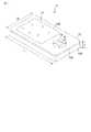
図1から図3に示すように、携帯型記憶装置11は、筐体12、プリント回路板13、液晶表示装置14、ハードディスク装置15、手動入力装置16、および電池17を備えている。筐体12は、樹脂により扁平な箱型に形成されている。筐体12は、厚み方向に2分割された第1の半部12Aと、第2の半部12Bとを有している。図2に示すように、筐体12は、厚み方向において互いに向かい合う第1の壁部12Cと第2の壁部12Dとを有している。第1の壁部12Cは、液晶表示装置14を外部に露出させるための開口12Eを有している。筐体12は、例えば、幅寸法Wが60mm、奥行き寸法Lが110mm、および厚み寸法Tが16mmで形成されている。筐体12の肉厚は、例えば1mmである。 As shown in FIGS. 1 to 3, the
記憶機構の一例であるハードディスク装置15は、筐体12の内部で、第2の壁部12Dに寄った位置に収容されている。ハードディスク装置15は、金属製の扁平なハウジングと、ハウジング内に収容されるディスクと、磁気ヘッドを有するキャリッジと、を有している。ハードディスク装置15の厚み寸法Aは、例えば、5mmである。もっとも、記憶機構としては、ハードディスク装置15に限られるものではない。記憶機構は、データ不揮発性のICメモリであるフラッシュメモリ等であってもよい。 The
電池17は、携帯型記憶装置11の電源として機能する。電池17の厚み寸法Bは、例えば、9mmである。 The
液晶表示装置14は、後述するアンテナ素子24による無線通信に悪影響を及ぼす部品の一例である。液晶表示装置14は、筐体12の内部で、第1の壁部12Cに寄った位置に収容される。液晶表示装置14は、第1の壁部12Cの開口12Eに臨んでいる。液晶表示装置14は、図示省略したが、例えば、ガラス基板、偏向板、液晶層、カラーフィルタ、バックライト、および透明電極などを有している。透明電極は、例えば、インジウムスズ酸化物(ITO:Indium-tin-oxide)で形成される。透明電極は、複数の配線が縦方向に延びている第1の部分と、複数の配線が横方向に延びている第2の部分とを有している。このため、透明電極は、全体として格子形状をなしており、電波吸収性を有する。液晶表示装置14は、後述するプリント配線板22の第1の面22Aに近接している。液晶表示装置14の厚み寸法Cは、例えば、3mmである。このため、前記ハードディスク装置15の厚み寸法Aは、液晶表示装置14の厚み寸法Cよりも大きくなっている。 The liquid
手動入力装置16は、後述するアンテナ素子24による無線通信に悪影響を及ぼす部品の一例である。手動入力装置16は、記憶機構であるハードディスク装置15を操作するために用いられる。手動入力装置16は、例えば、複数の入力用ボタン21を有している。ユーザが入力用ボタン21を操作すると、ハードディスク装置15に対して、データの記録およびデータの読み出しなどを指示できる。手動入力装置16の周囲に位置する筐体12の一部は、ユーザが使用する際に把持する部分になる。手動入力装置16は、プリント配線板22の後述する第1の面22Aに近接している。手動入力装置16の厚み寸法Dは、例えば、4mmである。 The
図4に示すように、プリント回路板13は、筐体12の内部で、液晶表示装置14と記憶機構であるハードディスク装置15との間の位置に収容されている。プリント回路板13は、プリント配線板22と、プリント配線板22に実装された主要な回路部品23と、プリント配線板22に実装されたアンテナ素子24と、イヤホン用のプラグが差し込まれるジャック25と、を備えている。 As shown in FIG. 4, the printed
図5に示すように、プリント配線板22は、方形の板状に形成されている。プリント配線板22は、液晶表示装置14、手動入力装置16、および主要な回路部品23に近接する第1の面22Aと、第1の面22Aとは反対側の第2の面22Bとを有している。プリント配線板22の第2の面22Bは、液晶表示装置14に対応する第1の領域26Aと、液晶表示装置14から外れている第2の領域26Bと、を有している。また、プリント配線板22の第2の面22Bは、手動入力装置16に対応する第1の領域27Aと、手動入力装置16から外れている第2の領域27Bと、を有している。さらに、プリント配線板22の第2の面22Bは、主要な回路部品23に対応する第1の領域28Aと、主要な回路部品23から外れている第2の領域28Bと、を有している。プリント配線板22は、第1の角部22Cと、第1の角部22Cと離れている第2の角部22Dとを有している。 As shown in FIG. 5, the printed
プリント配線板22の厚み寸法Eは、例えば0.8mmである。プリント配線板22は、さらに、上記電池17を通すための開口部22Eを有している。この携帯型記憶装置11では、開口部22Eに電池17が通されて薄型化が図られている。開口部22Eに通された電池17は、プリント配線板22を、主要な回路部品23が実装される部分と、アンテナ素子24が実装される部分とに分断する。これにより、主要な回路部品23からアンテナ素子24が隔離され、主要な回路部品23から生ずる不必要な電磁波の輻射からアンテナ素子24を守ることができる。 The thickness dimension E of the printed
プリント配線板22は、さらに、アンテナ素子24に接続される第1のグランド層31と、主要な回路部品23が実装される部分に対応する第2のグランド層32とを備えている。この第1のグランド層31は、第2のグランド層32から独立している。第1のグランド層31と、第2のグランド層32とは、いずれも銅薄膜により構成されている。第1のグランド層31は、アンテナ素子24から発信された電波の一部を外部に輻射しており、アンテナ素子24の無線通信の性能を向上させている。 The printed
ジャック25は、アンテナ素子24による無線通信に悪影響を及ぼす部品の一例である。ジャック25は、プリント配線板22の第2の面22Bの前記第1の角部22Cに実装されている。ジャック25は、例えば円筒形状に形成されている。ジャック25は、金属部品を含んでおり、電波吸収性を有する。筐体12は、ジャック25の近傍に貫通孔33を有しており、ジャック25を外部に露出させている。 The
主要な回路部品23は、アンテナ素子24による無線通信に悪影響を及ぼす部品の一例である。図4に示すように、主要な回路部品23は、例えば、CPU34と、ROM(Read Only Memory)35と、RAM(Random Access Memory)36と、アンテナ素子24の無線通信を駆動するための無線モジュール37と、その他の回路部品38などを含んでいる。本実施形態では、無線モジュール37は、ワイヤレスランチップ(W−LANチップ)で構成される。CPU34、ROM35、RAM36、無線モジュール37、およびその他の回路部品38は、図示しない複数の配線によって互いに電気的に接続されている。CPU34、ROM35、RAM36、無線モジュール37、その他の回路部品38は、携帯型記憶装置11の電源がオンとなった状態において、互いに膨大な量の制御データ、タイミングをとるためのクロック信号、およびRAM36のアドレスなどをやり取りする。このため、主要な回路部品23から電磁波が発生し、この電磁波は、アンテナ素子24の無線通信に悪影響を及ぼす可能性がある。 The
アンテナ素子24は、無線通信用の電波を送受信するチップ部品である。アンテナ素子24は、プリント配線板22の第2の面22Bの前記第2の角部22Dに実装されている。また、アンテナ素子24は、第2の面22Bの第2の領域26B、27B、28Bに相当する位置に実装されている。このため、アンテナ素子24は、液晶表示装置14、手動入力装置16、および主要な回路部品23から外れた位置に配置されており、これらによる悪影響から逃れている。 The
また、アンテナ素子24は、ハードディスク装置15や、電池17からも外れた位置に配置している。このため、アンテナ素子24で送受信される電波が、ハードディスク装置15や、電池17によって吸収されることがない。アンテナ素子24により、ホットスポットと呼ばれるアクセスポイントの近くでインターネットに接続したり、携帯型記憶装置11同士で、例えば、映像データや音楽データなどを交換したりすることができる。 The
また、プリント配線板22には、電気回路41が実装されている。図6に示すように、この電気回路41は、上記アンテナ素子24と、上記無線モジュール37と、アンテナ素子24と無線モジュール37とを接続するための信号線42と、アンテナ素子24の近傍で信号線42の途中に設けられる第1のマッチング回路43と、無線モジュール37の近傍で信号線42の途中に設けられる第2のマッチング回路44と、を有している。信号線42は、アンテナ素子24との間で信号をやりとりして、その信号を無線モジュール37に伝達することができる。 An
信号線42は、アンテナ素子24による無線通信に悪影響を及ぼす部品の一例である。信号線42は、同軸ケーブル45を含んでいる。同軸ケーブル45は、第1のマッチング回路43と、第2のマッチング回路44とを接続している。同軸ケーブル45は、金属部品を含んでおり、アンテナ素子24によって送受信される電波を吸収する性質を有する。同軸ケーブル45は、その一端において、コネクタ46を介して第1のマッチング回路43に接続されている。また、同軸ケーブル45は、その他端において、コネクタ47を介して第2のマッチング回路44に接続されている。同軸ケーブル45は、プリント配線板22の第1の面22Aに実装されており、第1の面22Aに近接している。同軸ケーブル45は、無線モジュール37とアンテナ素子24との間で、周囲に電磁波が漏洩することを防止する。 The
第1のマッチング回路43および第2のマッチング回路44は、電気回路41全体のインピーダンスを例えば50Ωに整合する。本実施形態では、マッチング回路が2箇所に設けられているため、電気回路41全体のインピーダンスの整合がより厳密になされる。上記したアンテナ素子24は、信号線42が設けられる第1の面22Aとは反対側の第2の面22Bに配置されており、信号線42による悪影響から逃れている。 The
携帯型記憶装置11から電波を発信する際には、無線モジュール37は、アンテナ素子24に向けて信号を送信する。この信号は、第2のマッチング回路44、コネクタ47、同軸ケーブル45、コネクタ46、および第1のマッチング回路43を経由して、アンテナ素子24に伝達される。そして、この信号は、アンテナ素子24およびこれに連なる第1のグランド層31において、電波として外部に輻射される。 When transmitting radio waves from the
一方、携帯型記憶装置11が外部から電波を受信する際には、アンテナ素子24で受信した信号は、第1のマッチング回路43、コネクタ46、同軸ケーブル45、コネクタ46、および第2のマッチング回路44を経由して、無線モジュール37に伝達される。これにより、携帯型記憶装置11は、外部から音楽データや画像データを受信することができる。その際、電気回路41のインピーダンスが厳密に整合されているため、受信した信号がロスなく無線モジュール37に伝達される。 On the other hand, when the
続いて、図2と図7を参照して、この携帯型記憶装置11の使用状態について説明する。この携帯型記憶装置11を机の天板51上に置いて使用する際には、通常ユーザは、図2に示すように、液晶表示装置14を上側にして天板51上に置いて使用する。そして、液晶表示装置14に表示される画面を見ながら、手動入力装置16を操作する。 Next, the usage state of the
本実施形態では、ハードディスク装置15の厚み寸法Aは、液晶表示装置14の厚み寸法Cよりも大きいため、プリント配線板22は、筐体12の厚み寸法Tにおける中間部よりも上側に配置している。このため、プリント配線板22に実装されたアンテナ素子24と天板51との間には、所定長の隙間Sが確保される。これにより、アンテナ素子24を天板51から離れた位置に配置して、無線通信を安定化することができる。 In the present embodiment, since the thickness dimension A of the
図7に示すように、ユーザが携帯型記憶装置11を手で持った状態で、これを使用する場合には、携帯型記憶装置11は、手動入力装置16の付近の筐体12の一部が手によって把持される。アンテナ素子24は、プリント配線板22の第2の面22Bで、手動入力装置16から外れている第2の領域27Bに配置されている。このため、ユーザの手によって、アンテナ素子24の無線通信が妨げられることが回避されている。 As shown in FIG. 7, when the user uses the
なお、本実施形態では、図5に示すように、ジャック25は、第2の角部22Dに隣接する第1の角部22Cに設けられているが、これに限定されるものではない。ジャック25は、第2の角部22Dとは対角の位置にある角部22Fに実装してもよい。 In the present embodiment, as shown in FIG. 5, the
以上が、携帯型記憶装置11の実施形態である。本実施形態によれば、アンテナ素子24は、無線通信に悪影響を及ぼす部品に近接している第1の面22Aとは反対側の第2の面22Bに実装されている。このため、この部品の影響を低減して、アンテナ素子24による無線通信を安定的に行うことができる。 The above is the embodiment of the
この場合、上記部品は、アンテナ素子24との間で信号をやりとりする信号線42、つまり同軸ケーブル45である。このため、同軸ケーブル45とアンテナ素子24とをプリント配線板22の同じ面に実装すると、信号線42自体や同軸ケーブル45の金属部品によってアンテナ素子24が送受信する電波が吸収されることになるが、この構成によれば、アンテナ素子24の送受信する電波がこれらによって吸収されてしまうことを防止できる。 In this case, the component is a
プリント配線板22の第2の面22Bは、アンテナ素子24に接続される第1のグランド層31を有し、この第1のグランド層31は、アンテナ素子24による無線通信の性能を向上させる。この構成によれば、アンテナ素子24により送信される電波の輻射性能の向上を図り、無線通信の特性を良好にできる。また、第1のグランド層31は、信号線42に近接している第1の面22Aとは反対側の第2の面22Bに設けられるため、この信号線42によって第1のグランド層31の効果が妨げられることを防止できる。さらに、第1のグランド層31は、同軸ケーブル45の裏側の位置に設けられるため、プリント配線板22上に別途に設置スペースを設ける必要がなく、プリント配線板22上のレイアウトを効率的に行うことができる。 The
プリント配線板22の第2の面22Bは、上記部品に対応する第1の領域26A、27A、28Aと、上記部品から外れている第2の領域26B、27B、28Bとを有し、アンテナ素子24は、第2の領域26B、27B、28Bに実装される。この構成によれば、無線通信に悪影響を及ぼす部品から離れた位置にアンテナ素子24を実装することができる。 The
この場合、上記部品は、液晶表示装置14であり、この液晶表示装置14は、格子形状をなした電極を有している。この構成によれば、アンテナ素子24を、液晶表示装置14から外れている第2の領域26Bに配置できる。このため、液晶表示装置14の電波吸収性によってアンテナ素子24の無線通信が妨げられることを防いで、無線通信を安定化できる。 In this case, the component is a liquid
この場合、上記部品は、記憶機構であるハードディスク装置15を操作するための手動入力装置16である。よって、アンテナ素子24は、手動入力装置16から外れている第2の領域27Bに配置される。ユーザは、手動入力装置16周りの筐体12の一部を把持して携帯型記憶装置11を使用する。一般に、人体は、電波吸収性を有することが知られている。上記構成によれば、アンテナ素子24をユーザが把持する領域から外れた位置に配置することができる。これにより、ユーザの手が、アンテナ素子24の無線通信に対して悪影響を及ぼす事態を防止できる。 In this case, the component is a
この場合、上記部品は、プリント配線板22の第1の面22Aに実装された主要な回路部品23である。よって、アンテナ素子24は、主要な回路部品23から外れている第2の領域28Bに配置される。この構成によれば、主要な回路部品23から発信される電磁波の影響によって、無線通信が乱されることを回避して、アンテナ素子24による無線通信を安定化できる。 In this case, the component is a
ジャック25は、プリント配線板22の第1の角部22Cに実装されるとともに、アンテナ素子24は、プリント配線板22の第2の角部22Dに実装される。この構成によれば、アンテナ素子24の周囲には、自由空間が確保されるため、アンテナ素子24による無線の通信特性を良好にできる。また、電波吸収性のある金属製のジャック25をアンテナ素子24から極力遠い位置に配置することができる。これにより、ジャック25が、アンテナ素子24の無線通信に悪影響を及ぼす事態を回避できる。 The
液晶表示装置14は、筐体12内の第1の壁部12Cに寄った位置に収容され、ハードディスク装置15は、筐体12内の第2の壁部12Dに寄った位置に収容されるとともに、プリント配線板22は、筐体12内の液晶表示装置14とハードディスク装置15との間の位置に収容される。また、ハードディスク装置15の厚み寸法は、液晶表示装置14の厚み寸法よりも大きい。これらの構成によれば、液晶表示装置14を上側に、ハードディスク装置15を下側にして、携帯型記憶装置11を机の天板51に載置して使用する際に、アンテナ素子24を天板51から離れた位置に配置することができる。これにより、机の天板51による電波吸収の影響を排除して、アンテナ素子24による無線通信を安定化できる。 The liquid
電気回路41は、アンテナ素子24の近傍で信号線42の途中に設けられる第1のマッチング回路43と、無線モジュール37の近傍で信号線42の途中に設けられる第2のマッチング回路44と、を具備している。この構成によれば、アンテナ素子24の近傍と、無線モジュール37の近傍との2箇所に第1および第2のマッチング回路43、44が設けられるため、電気回路41のインピーダンスの整合を厳密かつ容易に行うことができる。これにより、信号線42を通る信号の電損ロスを低減することができる。また、信号線42は、これらを接続する同軸ケーブル45を含み、同軸ケーブル45は、第1のマッチング回路43と第2のマッチング回路44とを接続する。この構成によれば、第1のマッチング回路43と第2のマッチング回路44との間で、外部に電磁波が漏れ出してしまうことを防止できる。これにより、アンテナ素子24による無線通信性能を向上できる。 The
本発明の電子機器および電気回路は、携帯型記憶装置用に限らず、例えば携帯電話機やポータブルコンピュータのようなその他の電子機器に対しても実施可能である。その他、電子機器および電気回路は、発明の要旨を逸脱しない範囲で種々変形して実施できることは勿論である。 The electronic device and the electric circuit of the present invention are not limited to the portable storage device, and can be implemented for other electronic devices such as a mobile phone and a portable computer. In addition, the electronic device and the electric circuit can be variously modified and implemented without departing from the scope of the invention.
A…厚み寸法、C…厚み寸法、11…携帯型記憶装置、12…筐体、12C…第1の壁部、12D…第2の壁部、12E…開口、14…液晶表示装置、15…ハードディスク装置、16…手動入力装置、17…電池、22…プリント配線板、22A…第1の面、22B…第2の面、22C…第1の角部、22D…第2の角部、23…主要な回路部品、24…アンテナ素子、25…ジャック、26A、27A、28A…第1の領域、26B、27B、28B…第2の領域、31…第1のグランド層、37…無線モジュール、41…電気回路、42…信号線、43…第1のマッチング回路、44…第2のマッチング回路、45…同軸ケーブルA ... thickness dimension, C ... thickness dimension, 11 ... portable storage device, 12 ... housing, 12C ... first wall portion, 12D ... second wall portion, 12E ... opening, 14 ... liquid crystal display device, 15 ... Hard disk device, 16 ... manual input device, 17 ... battery, 22 ... printed wiring board, 22A ... first surface, 22B ... second surface, 22C ... first corner, 22D ... second corner, 23 ... Major circuit components, 24 ... antenna element, 25 ... jack, 26A, 27A, 28A ... first region, 26B, 27B, 28B ... second region, 31 ... first ground layer, 37 ... wireless module, 41 ... Electric circuit, 42 ... Signal line, 43 ... First matching circuit, 44 ... Second matching circuit, 45 ... Coaxial cable
Claims (11)
Translated fromJapanese前記筐体の内部に収容される記憶機構と、
前記筐体の内部に収容されるプリント配線板と、
前記プリント配線板に実装されるとともに、無線通信を行うアンテナ素子と、
前記アンテナ素子による無線通信に悪影響を及ぼす部品と、
を具備し、
前記プリント配線板は、
前記部品に近接する第1の面と、
前記第1の面とは反対側の第2の面と、
を有し、
前記アンテナ素子は、前記第2の面に実装されることを特徴とする電子機器。A housing,
A storage mechanism housed in the housing;
A printed wiring board housed in the housing;
An antenna element that is mounted on the printed wiring board and performs wireless communication;
A component that adversely affects wireless communication by the antenna element;
Comprising
The printed wiring board is
A first surface proximate to the component;
A second surface opposite to the first surface;
Have
The electronic device is characterized in that the antenna element is mounted on the second surface.
前記アンテナ素子は、前記第2の領域に実装されることを特徴とする請求項1に記載の電子機器。The second surface of the printed wiring board has a first region corresponding to the component, and a second region that is detached from the component;
The electronic device according to claim 1, wherein the antenna element is mounted in the second region.
前記筐体の内部に収容される記憶機構と、
前記筐体の内部に収容されるプリント配線板と、
前記プリント配線板に実装されるとともに、無線通信を行うアンテナ素子と、
前記プリント配線板に実装されるとともに、前記アンテナ素子による無線通信に悪影響を及ぼす部品と、
を具備し、
前記プリント配線板は、
前記部品が実装される第1の角部と、
前記第1の角部と離れている第2の角部と、
を有し、
前記アンテナ素子は、前記第2の角部に実装されることを特徴とする電子機器。A housing,
A storage mechanism housed in the housing;
A printed wiring board housed in the housing;
An antenna element that is mounted on the printed wiring board and performs wireless communication;
A component that is mounted on the printed wiring board and adversely affects wireless communication by the antenna element;
Comprising
The printed wiring board is
A first corner on which the component is mounted;
A second corner away from the first corner;
Have
The electronic device is characterized in that the antenna element is mounted on the second corner.
前記筐体内の前記第1の壁部に寄った位置に収容されるとともに、前記第1の壁部に形成された開口に臨む液晶表示装置と、
前記筐体内の前記第2の壁部に寄った位置に収容される記憶機構と、
前記筐体内の前記液晶表示装置と前記記憶機構との間の位置に収容されるプリント配線板と、
前記プリント配線板に実装されるとともに、無線通信を行うアンテナ素子と、
を具備し、
前記記憶機構の厚み寸法は、前記液晶表示装置の厚み寸法よりも大きいことを特徴とする電子機器。A housing having a first wall portion and a second wall portion facing each other in the thickness direction;
A liquid crystal display device accommodated in a position near the first wall portion in the housing and facing an opening formed in the first wall portion;
A storage mechanism housed at a position near the second wall in the housing;
A printed wiring board housed in a position between the liquid crystal display device and the storage mechanism in the housing;
An antenna element that is mounted on the printed wiring board and performs wireless communication;
Comprising
The electronic device according to claim 1, wherein a thickness dimension of the storage mechanism is larger than a thickness dimension of the liquid crystal display device.
前記アンテナ素子を駆動する無線モジュールと、
前記アンテナ素子と前記回路部品とを接続する信号線と、
前記アンテナ素子の近傍で前記信号線の途中に設けられる第1のマッチング回路と、
前記無線モジュールの近傍で前記信号線の途中に設けられる第2のマッチング回路と、
を具備し、
前記信号線は、同軸ケーブルを含み、この同軸ケーブルは、前記第1のマッチング回路と前記第2のマッチング回路とを接続することを特徴とする電気回路。An antenna element for wireless communication;
A wireless module for driving the antenna element;
A signal line connecting the antenna element and the circuit component;
A first matching circuit provided in the middle of the signal line in the vicinity of the antenna element;
A second matching circuit provided in the middle of the signal line in the vicinity of the wireless module;
Comprising
The signal line includes a coaxial cable, and the coaxial cable connects the first matching circuit and the second matching circuit.
Priority Applications (2)
| Application Number | Priority Date | Filing Date | Title |
|---|---|---|---|
| JP2006237956AJP2008061109A (en) | 2006-09-01 | 2006-09-01 | Electronic equipment and electrical circuits |
| US11/889,008US7864122B2 (en) | 2006-09-01 | 2007-08-08 | Electronic device |
Applications Claiming Priority (1)
| Application Number | Priority Date | Filing Date | Title |
|---|---|---|---|
| JP2006237956AJP2008061109A (en) | 2006-09-01 | 2006-09-01 | Electronic equipment and electrical circuits |
Publications (1)
| Publication Number | Publication Date |
|---|---|
| JP2008061109Atrue JP2008061109A (en) | 2008-03-13 |
Family
ID=39150737
Family Applications (1)
| Application Number | Title | Priority Date | Filing Date |
|---|---|---|---|
| JP2006237956APendingJP2008061109A (en) | 2006-09-01 | 2006-09-01 | Electronic equipment and electrical circuits |
Country Status (2)
| Country | Link |
|---|---|
| US (1) | US7864122B2 (en) |
| JP (1) | JP2008061109A (en) |
Cited By (2)
| Publication number | Priority date | Publication date | Assignee | Title |
|---|---|---|---|---|
| JP2016131811A (en)* | 2015-01-21 | 2016-07-25 | シチズンホールディングス株式会社 | Electronic blood pressure monitor |
| JP2016220825A (en)* | 2015-05-28 | 2016-12-28 | シチズン時計株式会社 | Electronic manometer |
Families Citing this family (8)
| Publication number | Priority date | Publication date | Assignee | Title |
|---|---|---|---|---|
| CN102270316B (en) | 2005-03-31 | 2015-08-26 | 株式会社半导体能源研究所 | Wireless chip and there is the electronic equipment of wireless chip |
| CN102480869B (en)* | 2010-11-29 | 2015-02-04 | 富泰华工业(深圳)有限公司 | Shell component and electronic device with shell component |
| GB201205431D0 (en)* | 2012-03-28 | 2012-05-09 | Yota Devices Ipr Ltd | Display device antenna |
| JP2013254375A (en)* | 2012-06-07 | 2013-12-19 | Fujitsu Component Ltd | Touch panel and process of manufacturing the same |
| JP7330143B2 (en) | 2020-06-25 | 2023-08-21 | 株式会社東芝 | disk device |
| JP7286594B2 (en) | 2020-07-30 | 2023-06-05 | 株式会社東芝 | disk device |
| CN112233566B (en)* | 2020-11-23 | 2022-12-27 | 维沃移动通信有限公司 | Display screen and electronic equipment |
| JP7487132B2 (en)* | 2021-03-18 | 2024-05-20 | 株式会社東芝 | Disk device and electronic device |
Citations (6)
| Publication number | Priority date | Publication date | Assignee | Title |
|---|---|---|---|---|
| JPH0779110A (en)* | 1993-09-06 | 1995-03-20 | Sony Corp | Radio telephone set |
| JPH1131909A (en)* | 1997-05-14 | 1999-02-02 | Murata Mfg Co Ltd | Mobile communication device |
| JPH11145726A (en)* | 1997-08-09 | 1999-05-28 | Samsung Electron Co Ltd | Antenna circuit |
| JP2001077611A (en)* | 1999-09-06 | 2001-03-23 | Tdk Corp | Movable object communication machine |
| JP2003273622A (en)* | 2002-03-13 | 2003-09-26 | Toshiba Corp | Electronic device |
| JP2006506928A (en)* | 2002-10-22 | 2006-02-23 | シーメンス アクチエンゲゼルシヤフト | Wireless communication device and associated coupling structure comprising at least one printed circuit board and a flat antenna coupled thereto |
Family Cites Families (7)
| Publication number | Priority date | Publication date | Assignee | Title |
|---|---|---|---|---|
| JP2001345419A (en) | 2000-05-31 | 2001-12-14 | Hitachi Ltd | Integrated high frequency radio circuit module |
| JP3629211B2 (en)* | 2001-01-16 | 2005-03-16 | 株式会社東芝 | Electronics |
| JP3798733B2 (en) | 2001-06-13 | 2006-07-19 | 株式会社東芝 | Wireless module and wireless communication terminal provided with the wireless module |
| JP2005347912A (en) | 2004-06-01 | 2005-12-15 | Shinko Electric Ind Co Ltd | Antenna substrate |
| US7423605B2 (en)* | 2006-01-13 | 2008-09-09 | Research In Motion Limited | Mobile wireless communications device including an electrically conductive director element and related methods |
| US7548208B2 (en)* | 2006-02-24 | 2009-06-16 | Palm, Inc. | Internal diversity antenna architecture |
| US7561107B2 (en)* | 2006-09-07 | 2009-07-14 | Intelleflex Corporation | RFID device with microstrip antennas |
- 2006
- 2006-09-01JPJP2006237956Apatent/JP2008061109A/enactivePending
- 2007
- 2007-08-08USUS11/889,008patent/US7864122B2/enactiveActive
Patent Citations (6)
| Publication number | Priority date | Publication date | Assignee | Title |
|---|---|---|---|---|
| JPH0779110A (en)* | 1993-09-06 | 1995-03-20 | Sony Corp | Radio telephone set |
| JPH1131909A (en)* | 1997-05-14 | 1999-02-02 | Murata Mfg Co Ltd | Mobile communication device |
| JPH11145726A (en)* | 1997-08-09 | 1999-05-28 | Samsung Electron Co Ltd | Antenna circuit |
| JP2001077611A (en)* | 1999-09-06 | 2001-03-23 | Tdk Corp | Movable object communication machine |
| JP2003273622A (en)* | 2002-03-13 | 2003-09-26 | Toshiba Corp | Electronic device |
| JP2006506928A (en)* | 2002-10-22 | 2006-02-23 | シーメンス アクチエンゲゼルシヤフト | Wireless communication device and associated coupling structure comprising at least one printed circuit board and a flat antenna coupled thereto |
Cited By (2)
| Publication number | Priority date | Publication date | Assignee | Title |
|---|---|---|---|---|
| JP2016131811A (en)* | 2015-01-21 | 2016-07-25 | シチズンホールディングス株式会社 | Electronic blood pressure monitor |
| JP2016220825A (en)* | 2015-05-28 | 2016-12-28 | シチズン時計株式会社 | Electronic manometer |
Also Published As
| Publication number | Publication date |
|---|---|
| US7864122B2 (en) | 2011-01-04 |
| US20080055166A1 (en) | 2008-03-06 |
Similar Documents
| Publication | Publication Date | Title |
|---|---|---|
| JP2008061109A (en) | Electronic equipment and electrical circuits | |
| JP6197757B2 (en) | Interface and communication device | |
| US8058559B2 (en) | Flexible printed circuit board and electronic apparatus | |
| JP6652654B2 (en) | laptop | |
| JP2003140773A (en) | Wireless communication device and information processing apparatus | |
| KR20190041252A (en) | Display including bending area and electronic device with the same | |
| JP2014154777A (en) | Connection device | |
| JP2021170847A (en) | Electronics | |
| TWI405366B (en) | Wireless communciating devide and portable electronic apparatus using the same | |
| US20110068994A1 (en) | Communication module, communication apparatus | |
| JP2013222271A (en) | Electronic apparatus and conversion adapter | |
| US7304858B2 (en) | Printed circuit board unit and electronic apparatus | |
| JP2006178647A (en) | Information terminal device | |
| JP2011172095A (en) | Antenna and coupler | |
| JP2008244879A (en) | Portable wireless terminal | |
| JP5148078B2 (en) | Circuit module and electronic device | |
| JP2011076489A (en) | Information processing apparatus | |
| JP2019102835A (en) | Electronic equipment | |
| JP2009124610A (en) | Portable wireless device | |
| JP6665081B2 (en) | Electronics | |
| TWM666702U (en) | Antenna module and electronic device | |
| JP2009110411A (en) | Information processing device | |
| CN204883502U (en) | Panel computer mainboard and panel computer with SIM cassette and micro SIM cassette | |
| JP4615582B2 (en) | Electronics | |
| JP2006238232A (en) | Electronic device and cover member |
Legal Events
| Date | Code | Title | Description |
|---|---|---|---|
| A621 | Written request for application examination | Free format text:JAPANESE INTERMEDIATE CODE: A621 Effective date:20081006 | |
| A977 | Report on retrieval | Free format text:JAPANESE INTERMEDIATE CODE: A971007 Effective date:20100913 | |
| A131 | Notification of reasons for refusal | Free format text:JAPANESE INTERMEDIATE CODE: A131 Effective date:20100928 | |
| A521 | Request for written amendment filed | Free format text:JAPANESE INTERMEDIATE CODE: A523 Effective date:20101129 | |
| A02 | Decision of refusal | Free format text:JAPANESE INTERMEDIATE CODE: A02 Effective date:20101221 |