JP2008060099A - Thin film transistor and manufacturing method thereof - Google Patents
Thin film transistor and manufacturing method thereofDownload PDFInfo
- Publication number
- JP2008060099A JP2008060099AJP2006231515AJP2006231515AJP2008060099AJP 2008060099 AJP2008060099 AJP 2008060099AJP 2006231515 AJP2006231515 AJP 2006231515AJP 2006231515 AJP2006231515 AJP 2006231515AJP 2008060099 AJP2008060099 AJP 2008060099A
- Authority
- JP
- Japan
- Prior art keywords
- film
- thin film
- forming
- ohmic contact
- zinc oxide
- Prior art date
- Legal status (The legal status is an assumption and is not a legal conclusion. Google has not performed a legal analysis and makes no representation as to the accuracy of the status listed.)
- Granted
Links
Images


Landscapes
- Electrodes Of Semiconductors (AREA)
- Thin Film Transistor (AREA)
Abstract
Description
Translated fromJapaneseこの発明は薄膜トランジスタおよびその製造方法に関する。 The present invention relates to a thin film transistor and a method for manufacturing the same.
薄膜トランジスタを備えた液晶表示装置で用いられる透明導電膜には、透明性と低抵抗化を要求されることから、透明性を有する真性の酸化亜鉛(ZnO)膜では高抵抗であるが、n型不純物(例えばガリウム)がドーピングされた酸化亜鉛膜では低抵抗となるので、このようなn型不純物がドーピングされた酸化亜鉛膜によって形成するようにしたものがある(例えば、特許文献1参照)。 Since a transparent conductive film used in a liquid crystal display device including a thin film transistor is required to have transparency and low resistance, an intrinsic zinc oxide (ZnO) film having transparency has high resistance, but n-type Since a zinc oxide film doped with an impurity (for example, gallium) has a low resistance, there is one formed by using a zinc oxide film doped with such an n-type impurity (see, for example, Patent Document 1).
ところで、n型不純物(ガリウム)がドーピングされた酸化亜鉛膜をスパッタリングにより成膜する方法としては、ガリウム−酸化亜鉛物(GaZnO)をターゲットとして成膜する方法、あるいは、ガリウムおよび亜鉛を別々のターゲットとして、酸素ガスを用いた反応性スパッタリングにより成膜する方法がある。 By the way, as a method of forming a zinc oxide film doped with an n-type impurity (gallium) by sputtering, a method of forming a film using gallium-zinc oxide (GaZnO) as a target, or using gallium and zinc as separate targets. There is a method of forming a film by reactive sputtering using oxygen gas.
しかしながら、ガリウム−酸化亜鉛物をターゲットとして成膜する方法では、ターゲットが化合物であるため、その精製が困難であり、すなわち、ターゲットの化学的均一性を得ることが困難であり、成膜されたn型酸化亜鉛膜にバラツキが生じてしまうという問題がある。一方、ガリウムおよび亜鉛を別々のターゲットとして成膜する方法では、ターゲットが2つであるため、成膜されたn型酸化亜鉛膜の化学的均一性を得ることが困難であり、成膜されたn型酸化亜鉛膜にバラツキが生じてしまうという問題がある。 However, in the method of forming a film using gallium-zinc oxide as a target, since the target is a compound, it is difficult to purify the target, that is, it is difficult to obtain chemical uniformity of the target. There is a problem that variations occur in the n-type zinc oxide film. On the other hand, in the method of forming a film using gallium and zinc as separate targets, since there are two targets, it is difficult to obtain chemical uniformity of the formed n-type zinc oxide film. There is a problem that variations occur in the n-type zinc oxide film.
そこで、この発明は、低抵抗の透明導電膜を酸化亜鉛によってバラツキが生じないように形成することができる薄膜トランジスタおよびその製造方法を提供することを目的とする。 Accordingly, an object of the present invention is to provide a thin film transistor capable of forming a transparent conductive film having a low resistance so as not to cause variation due to zinc oxide, and a method for manufacturing the same.
この発明は、上記目的を達成するため、成膜された酸化亜鉛膜上に窒化シリコン膜を成膜し、該窒化シリコン膜の成膜により、前記酸化亜鉛膜を低抵抗化するようにしたことを特徴とするものである。 In order to achieve the above object, according to the present invention, a silicon nitride film is formed on the formed zinc oxide film, and the resistance of the zinc oxide film is reduced by forming the silicon nitride film. It is characterized by.
この発明によれば、成膜された酸化亜鉛膜上に窒化シリコン膜を成膜することにより、バラツキが小さい低抵抗の透明導電膜を形成することができる。 According to the present invention, a low resistance transparent conductive film with little variation can be formed by forming a silicon nitride film on the formed zinc oxide film.
(第1実施形態)
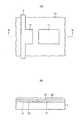
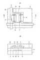
図1(A)はこの発明の第1実施形態としての薄膜トランジスタを備えた液晶表示装置の要部の透過平面図を示し、図1(B)は図1(A)のB−B線に沿う断面図を示す。この液晶表示装置はガラス基板1を備えている。ガラス基板1の上面側には、マトリクス状に配置された複数の画素電極2と、各画素電極2に接続された薄膜トランジスタ3と、行方向に配置され、各薄膜トランジスタ3に走査信号を供給する走査ライン4と、列方向に配置され、各薄膜トランジスタ3にデータ信号を供給するデータライン5とが設けられている。(First embodiment)
FIG. 1A shows a transmission plan view of a main part of a liquid crystal display device having a thin film transistor as a first embodiment of the present invention, and FIG. 1B is taken along line BB in FIG. A cross-sectional view is shown. The liquid crystal display device includes a
すなわち、ガラス基板1の上面の各所定の箇所にはアルミニウム、クロム、ITO等からなるソース電極11、ドレイン電極12および該ドレイン電極12に接続されたデータライン5が設けられている。ソース電極11の上面のドレイン電極12側には後述の如く低抵抗化された真性の酸化亜鉛(ZnO)膜からなる一方のオーミックコンタクト層13が設けられている。データライン5の一部を含むドレイン電極12の上面のソース電極11側には同じく後述の如く低抵抗化された真性の酸化亜鉛膜からなる他方のオーミックコンタクト層14が設けられている。 That is, a
この場合、オーミックコンタクト層13、14の互いに対向する端面13a、14aはソース電極11およびドレイン電極12の互いに対向する端面11a、12aと同一形状となっている。そして、オーミックコンタクト層13、14の端面11a、12aの間隔がチャネル長Lとなっており、オーミックコンタクト層13、14のチャネル長Lに直交する方向の寸法がチャネル幅Wとなっている。 In this case, the end faces 13 a and 14 a of the
オーミックコンタクト層13、14の上面には窒化シリコンからなる第1の保護膜15、16が設けられている。第1の保護膜15、16の中央部にはコンタクトホール17、18が設けられている。ここで、第1の保護膜15、16とオーミックコンタクト層13、14とは、図1(A)に図示される如く、平面外形形状が同一である。 On the upper surfaces of the
コンタクトホール17、18を介して露出されたオーミックコンタクト層13、14の上面を含む第1の保護膜15、16の上面全体およびその間のガラス基板1の上面には真性の酸化亜鉛(ZnO)からなる半導体薄膜19が設けられている。半導体薄膜19の上面全体には酸化シリコンからなる第2の保護膜20が設けられている。この場合、第2の保護膜20と半導体薄膜19とは、図1(A)に図示される如く、平面形状が同一である。 The entire upper surface of the first
第2の保護膜20、ソース電極11、ドレイン電極12およびデータライン5を含むガラス基板1の上面には窒化シリコンからなる絶縁膜21が設けられている。絶縁膜21の上面の各所定の箇所にはアルミニウム、クロム、ITO等からなるゲート電極22および該ゲート電極22に接続された走査ライン4が設けられている。 An
ここで、ソース電極11、ドレイン電極12、オーミックコンタクト層13、14、第1の保護膜15、16、半導体薄膜19、第2の保護膜20、絶縁膜21およびゲート電極22により、トツプゲート構造の薄膜トランジスタ3が構成されている。この場合、薄膜トランジスタ3のゲート絶縁膜は、第2の保護膜20および絶縁膜21によって形成されている。 Here, the
ゲート電極22および走査ライン4を含む絶縁膜21の上面には窒化シリコンからなるオーバーコート膜23が設けられている。ソース電極11の所定の箇所に対応する部分におけるオーバーコート膜23および絶縁膜21にはコンタクトホール24が設けられている。オーバーコート膜20の上面の所定の箇所にはITO等の透明導電材料からなる画素電極2がコンタクトホール24を介してソース電極11に接続されて設けられている。 An
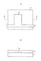
次に、この液晶表示装置の製造方法の一例について説明する。まず、図2(A)、(B)に示すように、ガラス基板1の上面の各所定の箇所に、スパッタリングにより成膜されたアルミニウム、クロム、ITO等からなる金属膜をフォトリソグラフィ法によりパターニングすることにより、ソース電極11、ドレイン電極12および該ドレイン電極12に接続されたデータライン5を形成する。 Next, an example of a manufacturing method of this liquid crystal display device will be described. First, as shown in FIGS. 2A and 2B, a metal film made of aluminum, chromium, ITO, or the like formed by sputtering at each predetermined location on the upper surface of the
次に、ソース電極11、ドレイン電極12およびデータライン5を含むガラス基板1の上面に真性の酸化亜鉛(ZnO)からなるオーミックコンタクト層形成用膜31を成膜する。この場合、オーミックコンタクト層形成用膜31の成膜は、亜鉛をターゲットとして、酸素ガスを用いた反応性スパッタリングにより行うと、ターゲットが1つで亜鉛のみからなるので、オーミックコンタクト層形成用膜31をバラツキが生じないように成膜することができる。また、この状態では、オーミックコンタクト層形成用膜31は成膜されただけの酸化亜鉛膜によって形成されているので、高抵抗である。 Next, an ohmic contact
次に、図3(A)、(B)に示すように、オーミックコンタクト層形成用膜31の上面に、プラズマCVD法により、窒化シリコンからなる第1の保護膜形成用膜32を成膜する。すると、酸化亜鉛からなるオーミックコンタクト層形成用膜31の抵抗が著しく低下し、低抵抗化される。 Next, as shown in FIGS. 3A and 3B, a first protective
ここで、ガラス基板上に成膜された膜厚500Åの酸化亜鉛膜について、その200μm×8μmの領域の8μm方向の両側から20Vの電圧を印加したところ、電流値は概ね1〜10pAであり、高抵抗であった。これに対し、酸化亜鉛膜の上面にプラズマCVD法により窒化シリコン膜を成膜し、上記と同様の条件で電圧を印加したところ、電流値は概ね200mAであり、4〜5桁大きくなり、低抵抗であった。また、この後に、窒化シリコン膜をドライエッチングにより除去しても、酸化亜鉛膜は低抵抗のままであった。 Here, when a voltage of 20 V is applied to both sides of the 200 μm × 8 μm region in the 8 μm direction of the 500 μm thick zinc oxide film formed on the glass substrate, the current value is approximately 1 to 10 pA. High resistance. On the other hand, when a silicon nitride film is formed on the upper surface of the zinc oxide film by a plasma CVD method and a voltage is applied under the same conditions as described above, the current value is approximately 200 mA, which is 4 to 5 orders of magnitude higher and lower. It was resistance. After that, even if the silicon nitride film was removed by dry etching, the zinc oxide film remained low resistance.
したがって、酸化亜鉛からなるオーミックコンタクト層形成用膜31の上面にプラズマCVD法により窒化シリコンからなる第1の保護膜形成用膜32を成膜すると、オーミックコンタクト層形成用膜31は低抵抗化される。また、この後に、後述するが、第1の保護膜形成用膜32の一部をドライエッチングにより除去して、オーミックコンタクト層形成用膜31の一部を露出させても、この露出されたオーミックコンタクト層形成用膜31は低抵抗のままである。 Therefore, when the first protective
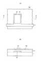
次に、図4(A)、(B)に示すように、第1の保護膜形成用膜32の上面の各所定の箇所に、フォトリソグラフィ法により、第1の保護膜15、16形成用のレジストパターン33a、33bを形成する。次に、レジストパターン33a、33bをマスクとして、第1の保護膜形成用膜32をエッチングすると、図5(A)、(B)に示すように、レジストパターン33a、33b下に第1の保護膜15、16が形成される。 Next, as shown in FIGS. 4A and 4B, the first
この場合、レジストパターン33a、33b下以外の領域における酸化亜鉛からなるオーミックコンタクト層形成用膜31の上面が露出される。ところで、酸化亜鉛は酸にもアルカリにも溶けやすく、エッチング耐性が極めて低い。そこで、窒化シリコンからなる第1の保護膜形成用膜32のエッチング方法は、第1の保護膜形成用膜32のエッチング速度は速いが、酸化亜鉛からなるオーミックコンタクト層形成用膜31をなるべく侵さないようにするために、六フッ化イオウ(SF6)を用いた反応性プラズマエッチング(ドライエッチング)が好ましい。 In this case, the upper surface of the ohmic contact
次に、レジストパターン33a、33bをレジスト剥離液を用いて剥離する。この場合、第1の保護膜15、16下以外の領域におけるオーミックコンタクト層形成用膜31の上面がレジスト剥離液に曝されるが、この曝された部分はデバイスエリア以外であるので、別に支障はない。すなわち、第1の保護膜15、16下のオーミックコンタクト層形成用膜31は第1の保護膜15、16によって保護されている。 Next, the resist
次に、第1の保護膜15、16をマスクとして、オーミックコンタクト層形成用膜31をエッチングすると、図6(A)、(B)に示すように、第1の保護膜15、16下にオーミックコンタクト層13、14が形成される。この場合、酸化亜鉛からなるオーミックコンタクト層形成用膜31のエッチング液としては、加工の制御性を良好とするため、アルカリ水溶液を用いる。例えば、水酸化ナトリウム(NaOH)30wt%未満水溶液、好ましくは2〜10wt%水溶液を用いる。エッチング液の温度は、5〜40℃、好ましくは室温(22〜23℃)とする。 Next, when the ohmic contact
そして、エッチング液として水酸化ナトリウム(NaOH)5wt%水溶液(温度は室温(22〜23℃))を用いたところ、エッチング速度は約80nm/分であった。ところで、エッチング速度は、加工の制御性を考慮した場合、余り大きいと膜厚や密度等のばらつきの要因のためエッチング終了の制御が難しく、勿論、小さすぎれば生産性が低下する。そこで、エッチング速度は、一般的に、100〜200nm/分程度が好ましいと言われている。エッチング速度が約80nm/分の水酸化ナトリウム(NaOH)5wt%水溶液は、一応、満足できる範囲と言える。 When an aqueous solution of sodium hydroxide (NaOH) 5 wt% (temperature is room temperature (22 to 23 ° C.)) was used as an etching solution, the etching rate was about 80 nm / min. By the way, when considering the controllability of processing, if the etching rate is too large, it is difficult to control the end of etching because of variations in film thickness, density, etc. Of course, if the etching rate is too small, the productivity is lowered. Therefore, it is generally said that the etching rate is preferably about 100 to 200 nm / min. A 5 wt% aqueous solution of sodium hydroxide (NaOH) with an etching rate of about 80 nm / min can be said to be a satisfactory range.
以上のようにして形成されたオーミックコンタクト層13、14では、上述の如く、その元となる酸化亜鉛からなるオーミックコンタクト層形成用膜31をバラツキが生じないように成膜することができ、且つ、窒化シリコンからなる第1の保護膜形成用膜32の成膜によりオーミックコンタクト層形成用膜31を低抵抗化することができるので、n型不純物を含まなくても、低抵抗でバラツキが生じないように形成することができる。 In the ohmic contact layers 13 and 14 formed as described above, as described above, the ohmic contact
なお、上記では、レジストパターン33a、33bを剥離した後、第1の保護膜15、16をマスクとして、オーミックコンタクト層形成用膜31をエッチングする順序としているが、オーミックコンタクト層形成用膜31をエッチングした後、レジストパターン33a、33bを剥離するようにしてもよい。 In the above description, after the resist
次に、図7(A)、(B)に示すように、フォトリソグラフィ法により、第1の保護膜15、16の中央部にコンタクトホール17、18を形成する。この場合、コンタクトホール17、18を介してオーミックコンタクト層13、14の上面が露出されるが、この露出されたオーミックコンタクト層13、14は低抵抗のままである。 Next, as shown in FIGS. 7A and 7B, contact holes 17 and 18 are formed in the central portions of the first
また、コンタクトホール17、18を介してオーミックコンタクト層13、14の上面が露出されるため、窒化シリコンからなる第1の保護膜15、16にコンタクトホール17、18を形成するためのエッチング方法としては、六フッ化イオウ(SF6)を用いた反応性プラズマエッチング(ドライエッチング)が好ましい。 Further, since the upper surfaces of the ohmic contact layers 13 and 14 are exposed through the contact holes 17 and 18, as an etching method for forming the contact holes 17 and 18 in the first
ところで、コンタクトホール13、14を形成するためのレジストパターン(図示せず)をレジスト剥離液を用いて剥離するとき、オーミックコンタクト層13、14の周側面およびコンタクトホール17、18を介して露出されたオーミックコンタクト層13、14の上面がレジスト剥離液に曝される。ここで、レジスト剥離液として、酸性もアルカリ性も呈さない(電解質を含まない)もの、例えば、単一の有機溶媒(例えばジメチルスルホキシド(DMSO))を用いても、レジスト剥離を良好に行えることは、発明者において確認されている。 By the way, when a resist pattern (not shown) for forming the contact holes 13 and 14 is stripped using a resist stripping solution, the resist pattern is exposed through the peripheral side surfaces of the ohmic contact layers 13 and 14 and the contact holes 17 and 18. The upper surfaces of the ohmic contact layers 13 and 14 are exposed to a resist stripping solution. Here, it is possible to perform resist stripping satisfactorily even if a resist stripping solution that does not exhibit acidity or alkalinity (no electrolyte), for example, a single organic solvent (for example, dimethyl sulfoxide (DMSO)) is used. Has been confirmed by the inventor.
そして、このレジスト剥離液により酸化亜鉛からなるオーミックコンタクト層13、14の周側面がエッチングされるが、その場合のサイドエッチング量はそれ程大きくなく、チャネル長Lに影響を与える程ではない。また、このレジスト剥離液によりコンタクトホール17、18を介して露出されたオーミックコンタクト層13、14の上面がエッチングされるが、オーミックコンタクト層13、14の膜減りは薄膜トランジスタの特性に影響を与えることがないので、問題はない。 The peripheral side surfaces of the ohmic contact layers 13 and 14 made of zinc oxide are etched by this resist stripping solution, but the side etching amount in that case is not so large and does not affect the channel length L. In addition, the upper surface of the ohmic contact layers 13 and 14 exposed through the contact holes 17 and 18 is etched by this resist stripping solution, but the film thickness reduction of the ohmic contact layers 13 and 14 affects the characteristics of the thin film transistor. There is no problem.
次に、図8(A)、(B)に示すように、コンタクトホール17、18を介して露出されたオーミックコンタクト層13、14の上面、第1の保護膜15、16、ソース電極11、ドレイン電極12およびデータライン5を含むガラス基板1の上面に、上記反応性スパッタリングにより、真性の酸化亜鉛からなる半導体薄膜形成用膜19aを成膜する。 Next, as shown in FIGS. 8A and 8B, the upper surfaces of the ohmic contact layers 13 and 14 exposed through the contact holes 17 and 18, the first
次に、半導体薄膜形成用膜19aの上面に、プラズマCVD法により、酸化シリコンからなる第2の保護膜形成用膜20aを成膜する。この場合、半導体薄膜形成用膜19aの上面に酸化シリコンからなる第2の保護膜形成用膜20aを成膜しても、半導体薄膜形成用膜19aは高抵抗のままであり、低抵抗化されることはない。 Next, a second protective
次に、第2の保護膜形成用膜20aの上面の所定の箇所に、フォトリソグラフィ法により、デバイスエリア形成用のレジストパターン34を形成する。次に、レジストパターン34をマスクとして、第2の保護膜形成用膜20aをエッチングすると、図9(A)、(B)に示すように、レジストパターン34下に第2の保護膜20が形成される。 Next, a resist
この場合、レジストパターン34下以外の領域における半導体薄膜形成用膜19aの上面が露出される。そこで、酸化シリコンからなる第2の保護膜形成用膜20aのエッチング方法としては、第2の保護膜形成用膜20aのエッチング速度は速いが、酸化亜鉛からなる半導体薄膜形成用膜19aをなるべく侵さないようにするために、六フッ化イオウ(SF6)を用いた反応性プラズマエッチング(ドライエッチング)が好ましい。 In this case, the upper surface of the semiconductor thin
次に、レジストパターン34をレジスト剥離液を用いて剥離する。この場合、第2の保護膜20下以外の領域における半導体薄膜形成用膜19aの上面がレジスト剥離液に曝されるが、この曝された部分はデバイスエリア以外であるので、別に支障はない。すなわち、第2の保護膜20下の半導体薄膜形成用膜19aは第2の保護膜20によって保護されている。 Next, the resist
なお、この場合のレジスト剥離液として、酸性もアルカリ性も呈さない(電解質を含まない)もの、例えば、単一の有機溶媒(例えばジメチルスルホキシド(DMSO))を用いてもよい。また、ここで、図5に示すレジストパターン33a、33bを剥離するためのレジスト剥離液として、酸性もアルカリ性も呈さない(電解質を含まない)もの、例えば、単一の有機溶媒(例えばジメチルスルホキシド(DMSO))を用いてもよい。 In this case, a resist stripping solution that does not exhibit acidity or alkalinity (no electrolyte), for example, a single organic solvent (for example, dimethyl sulfoxide (DMSO)) may be used. Further, here, as a resist stripping solution for stripping the resist
次に、第2の保護膜20をマスクとして、半導体薄膜形成用膜19aをエッチングすると、図10(A)、(B)に示すように、第2の保護膜20下に半導体薄膜19が形成される。この場合、酸化亜鉛からなる半導体薄膜形成用膜19aのエッチング液として上記水酸化ナトリウム水溶液を用いると、加工の制御性を良好とすることができる。ここで、オーミックコンタクト層13、14の間隔がチャネル長Lとなり、オーミックコンタクト層13、14のチャネル長Lに直交する方向の寸法がチャネル幅Wとなる。 Next, when the semiconductor thin
なお、上記では、レジストパターン34を剥離した後、第2の保護膜20をマスクとして、半導体薄膜形成用膜19aをエッチングする順序としているが、半導体薄膜形成用膜19aをエッチングした後、レジストパターン34を剥離するようにしてもよい。 In the above description, after the resist
次に、図1(A)、(B)に示すように、第2の保護膜20、ソース電極11、ドレイン電極12およびデータライン5を含むガラス基板1の上面に、プラズマCVD法により、窒化シリコンからなる絶縁膜21を成膜する。次に、絶縁膜21の上面の所定の箇所に、スパッタリングにより成膜されたクロム、アルミニウム、ITO等からなる金属膜をフォトリソグラフィ法によりパターニングすることにより、ゲート電極22および該ゲート電極22に接続された走査ライン4を形成する。 Next, as shown in FIGS. 1A and 1B, the upper surface of the
次に、ゲート電極22および走査ライン4を含む絶縁膜21の上面に、プラズマCVD法により、窒化シリコンからなるオーバーコート膜23を成膜する。次に、ソース電極15の所定の箇所に対応する部分におけるオーバーコート膜23および絶縁膜21に、フォトリソグラフィ法により、コンタクトホール24を連続して形成する。 Next, an
次に、オーバーコート膜20の上面の所定の箇所に、スパッタリングにより成膜されたITO等の透明導電材料からなる画素電極形成用膜をフォトリソグラフィ法によりパターニングすることにより、画素電極2をコンタクトホール24を介してソース電極11に接続させて形成する。かくして、図1(A)、(B)に示す液晶表示装置が得られる。 Next, a pixel electrode forming film made of a transparent conductive material such as ITO formed by sputtering is patterned at a predetermined position on the upper surface of the
(第2実施形態)
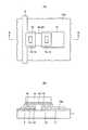
図11(A)はこの発明の第2実施形態としての薄膜トランジスタを備えた液晶表示装置の要部の透過平面図を示し、図11(B)は図11(A)のB−B線に沿う断面図を示す。この液晶表示装置において、図1(A)、(B)に示す液晶表示装置と大きく異なる点は、薄膜トランジスタ3をボトムゲート構造とし、且つ、画素電極2、ゲート電極22、走査ライン4、ソース電極11、ドレイン電極12およびデータライン5を低抵抗化された真性の酸化亜鉛(ZnO)膜によって形成し、オーミックコンタクト層13、14をn型酸化亜鉛膜によって形成した点である。(Second Embodiment)
FIG. 11A shows a transmission plan view of a main part of a liquid crystal display device provided with a thin film transistor as a second embodiment of the present invention, and FIG. 11B is along the line BB in FIG. 11A. A cross-sectional view is shown. This liquid crystal display device is greatly different from the liquid crystal display device shown in FIGS. 1A and 1B in that the
すなわち、ガラス基板1の上面の各所定の箇所には低抵抗化された真性の酸化亜鉛(ZnO)膜からなるゲート電極22および該ゲート電極22に接続された走査ライン4が設けられている。ゲート電極22および走査ライン4を含むガラス基板1の上面には窒化シリコンからなるゲート絶縁膜41が設けられている。 That is, a
ゲート電極22上におけるゲート絶縁膜41の上面の所定の箇所には真の性酸化亜鉛(ZnO)からなる半導体薄膜19が設けられている。半導体薄膜19の上面中央部には酸化シリコンからなるチャネル保護膜42が設けられている。チャネル保護膜42の上面両側およびその両側における半導体薄膜19の上面にはn型酸化亜鉛からなるオーミックコンタクト層13、14が設けられている。 A semiconductor
一方のオーミックコンタクト層13の上面およびゲート絶縁膜41の上面の所定の箇所には低抵抗化された酸化亜鉛膜からなるソース電極11および該ソース電極11に接続された画素電極2が設けられている。他方のオーミックコンタクト層14の上面およびゲート絶縁膜41の上面の所定の箇所には低抵抗化された酸化亜鉛膜からなるドレイン電極12および該ドレイン電極12に接続されたデータライン5が設けられている。 A
ソース電極11、ドレイン電極12、チャネル保護膜42、データライン5および画素電極2を含むゲート絶縁膜41の上面には窒化シリコンからなるオーバーコート膜23が設けられている。画素電極2の外周部以外の領域に対応する部分におけるオーバーコート膜23には開口部43が設けられている。 An
次に、この液晶表示装置の製造方法の一例について説明する。まず、図12(A)、(B)に示すように、ガラス基板1の上面の各所定の箇所に、上記反応性スパッタリングにより成膜された酸化亜鉛膜をフォトリソグラフィ法によりパターニングすることにより、ゲート電極22および該ゲート電極22に接続された走査ライン4を形成する。この状態では、ゲート電極22および走査ライン4は成膜されてパターニングされただけの酸化亜鉛膜によって形成されているので、高抵抗である。 Next, an example of a manufacturing method of this liquid crystal display device will be described. First, as shown in FIGS. 12 (A) and 12 (B), by patterning the zinc oxide film formed by reactive sputtering at each predetermined location on the upper surface of the
次に、図13(A)、(B)に示すように、ゲート電極22および走査ライン4を含むガラス基板1の上面に、プラズマCVD法により、窒化シリコンからなるゲート絶縁膜41を成膜する。すると、酸化亜鉛からなるゲート電極22および走査ライン4の抵抗が著しく低下し、低抵抗化される。 Next, as shown in FIGS. 13A and 13B, a
この場合も、ゲート電極22および走査ライン4は、上記第1実施形態の場合と同様に、その元となる酸化亜鉛膜をバラツキが生じないように成膜することができ、且つ、窒化シリコンからなるゲート絶縁膜41の成膜により当該酸化亜鉛膜を低抵抗化することができるので、n型不純物を含まなくても、低抵抗でバラツキが生じないように形成することができる。 Also in this case, the
次に、図14(A)、(B)に示すように、ゲート絶縁膜41の上面に、上記反応性スパッタリングにより、酸化亜鉛からなる半導体薄膜形成用膜19aを成膜する。次に、半導体薄膜形成用膜19aの上面に、プラズマCVD法により、酸化シリコンからなるチャネル保護膜形成用膜42aを成膜する。この場合、半導体薄膜形成用膜19aの上面に酸化シリコンからなるチャネル保護膜形成用膜42aを成膜しても、半導体薄膜形成用膜19aは高抵抗のままであり、低抵抗化されることはない。 Next, as shown in FIGS. 14A and 14B, a semiconductor thin
次に、チャネル保護膜形成用膜42aをフォトリソグラフィ法によりパターニングすると、図15(A)、(B)に示すように、チャネル保護膜42が形成される。次に、図16(A)、(B)に示すように、チャネル保護膜42を含む半導体薄膜形成用膜19aの上面に、プラズマCVD法により、n型酸化亜鉛からなるオーミックコンタクト層形成用膜51を成膜する。 Next, when the channel protective
次に、オーミックコンタクト層形成用膜51および半導体薄膜形成用膜19aをフォトリソグラフィ法により連続してパターニングすると、図17(A)、(B)に示すように、オーミックコンタクト層13、14が形成され、且つ、オーミックコンタクト層13、14およびチャネル保護膜42下に半導体薄膜19が形成される。 Next, when the ohmic contact
次に、図18(A)、(B)に示すように、オーミックコンタクト層13、14の各上面およびゲート絶縁膜41の上面の各所定の箇所に、上記反応性スパッタリングにより成膜された酸化亜鉛膜をフォトリソグラフィ法によりパターニングすることにより、ソース電極11および該ソース電極11に接続された画素電極2と、ドレイン電極12および該ドレイン電極12に接続されたデータライン5とを形成する。この状態では、ソース電極11、画素電極2、ドレイン電極12およびデータライン5は成膜されてパターニングされただけの酸化亜鉛膜によって形成されているので、高抵抗である。 Next, as shown in FIGS. 18A and 18B, an oxidation film formed by reactive sputtering at each predetermined position on the upper surfaces of the ohmic contact layers 13 and 14 and the upper surface of the
次に、図19(A)、(B)に示すように、ソース電極11、画素電極2、ドレイン電極12およびデータライン5を含むゲート絶縁膜41の上面に、プラズマCVD法により、窒化シリコンからなるオーバーコート膜23を形成する。すると、酸化亜鉛からなるソース電極11、画素電極2、ドレイン電極12およびデータライン5の抵抗が著しく低下し、低抵抗化される。 Next, as shown in FIGS. 19A and 19B, the upper surface of the
この場合も、ソース電極11、画素電極2、ドレイン電極12およびデータライン5は、上記第1実施形態の場合と同様に、その元となる酸化亜鉛膜をバラツキが生じないように成膜することができ、且つ、窒化シリコンからなるオーバーコート膜23の成膜により当該酸化亜鉛膜を低抵抗化することができるので、n型不純物を含まなくても、低抵抗でバラツキが生じないように形成することができる。 Also in this case, the
次に、図11(A)、(B)に示すように、フォトリソグラフィ法により、画素電極2の外周部以外の領域に対応する部分におけるオーバーコート膜23に開口部43を形成する。この場合、画素電極2の外周部以外の領域は開口部43を介して露出されるが、この露出された領域は低抵抗のままである。かくして、図11(A)、(B)に示す液晶表示装置が得られる。 Next, as shown in FIGS. 11A and 11B, an
なお、上記実施形態においては、真性の酸化亜鉛膜上に窒化シリコン膜を形成するものであったが、不純物がドーピングされている酸化亜鉛膜上に窒化シリコン膜を形成する場合においても、バラツキが小さく低抵抗化された酸化亜鉛膜とすることができる。 In the above embodiment, the silicon nitride film is formed on the intrinsic zinc oxide film. However, even when the silicon nitride film is formed on the zinc oxide film doped with impurities, there is variation. A small and low resistance zinc oxide film can be obtained.
1 ガラス基板
2 走査ライン
3 データライン
4 画素電極
5 薄膜トランジスタ
11 ソース電極
12 ドレイン電極
13、14 オーミックコンタクト層
15、16 第1の保護膜
17、18 コンタクトホール
19 半導体薄膜
20 第2の保護膜
21 絶縁膜
22 ゲート電極
23 オーバーコート膜
24 コンタクトホール
41 ゲート絶縁膜
42 チャネル保護膜
43 開口部DESCRIPTION OF
Claims (24)
Translated fromJapanese前記オーミックコンタクト層形成用膜上に窒化シリコンからなる保護膜形成用膜を成膜し、且つ、該保護膜形成用膜の成膜により、前記オーミックコンタクト層形成用膜を低抵抗化する工程と、
フォトリソグラフィ法により前記保護膜形成用膜をパターニングすることにより、前記ソース電極および前記ドレイン電極上における前記オーミックコンタクト層形成用膜上に2つの保護膜を形成する工程と、
前記各保護膜をマスクとして前記オーミックコンタクト層形成用膜をエッチングすることにより、前記各保護膜下にオーミックコンタクト層を形成する工程と、
を有することを特徴とする薄膜トランジスタの製造方法。Forming an ohmic contact layer forming film made of zinc oxide on the source electrode and the drain electrode;
Forming a protective film forming film made of silicon nitride on the ohmic contact layer forming film, and reducing the resistance of the ohmic contact layer forming film by forming the protective film forming film; ,
Forming two protective films on the ohmic contact layer forming film on the source electrode and the drain electrode by patterning the protective film forming film by a photolithography method;
Etching the ohmic contact layer forming film using the protective films as masks to form ohmic contact layers under the protective films; and
A method for producing a thin film transistor, comprising:
酸化亜鉛からなるゲート電極形成用膜を成膜する工程と、
前記ゲート電極形成用膜上に窒化シリコンからなる前記ゲート絶縁膜を成膜し、且つ、該ゲート絶縁膜の成膜により、前記ゲート電極形成用膜を低抵抗化する工程と、
フォトリソグラフィ法により前記ゲート電極形成用膜をパターニングすることにより、前記ゲート電極を形成する工程と、
酸化亜鉛からなるソース・ドレイン電極形成用膜を成膜する工程と、
前記ソース・ドレイン電極形成用膜上に窒化シリコンからなる前記オーバーコート膜を成膜し、且つ、該オーバーコート膜の成膜により、前記ソース・ドレイン電極形成用膜を低抵抗化する工程と、
フォトリソグラフィ法により前記ソース・ドレイン電極形成用膜をパターニングすることにより、前記ソース電極および前記ドレイン電極を形成する工程と、
を有することを特徴とする薄膜トランジスタの製造方法。A semiconductor thin film; a gate insulating film provided under the semiconductor thin film; a gate electrode provided under the gate insulating film opposite to the semiconductor thin film; and a channel protection provided at a central portion of the upper surface of the semiconductor thin film A film, an ohmic contact layer provided on both sides of the upper surface of the channel protective film and on the upper surface of the semiconductor thin film on both sides thereof, a source electrode and a drain electrode provided on each ohmic contact layer, the source electrode and the In a method of manufacturing a thin film transistor having an overcoat film covering the drain electrode,
Forming a gate electrode forming film made of zinc oxide;
Forming the gate insulating film made of silicon nitride on the gate electrode forming film, and reducing the resistance of the gate electrode forming film by forming the gate insulating film;
Forming the gate electrode by patterning the gate electrode forming film by a photolithography method;
Forming a source / drain electrode forming film made of zinc oxide;
Forming the overcoat film made of silicon nitride on the source / drain electrode formation film, and reducing the resistance of the source / drain electrode formation film by forming the overcoat film;
Forming the source electrode and the drain electrode by patterning the source / drain electrode formation film by a photolithography method;
A method for producing a thin film transistor, comprising:
Priority Applications (1)
| Application Number | Priority Date | Filing Date | Title |
|---|---|---|---|
| JP2006231515AJP5332091B2 (en) | 2006-08-29 | 2006-08-29 | Thin film transistor manufacturing method |
Applications Claiming Priority (1)
| Application Number | Priority Date | Filing Date | Title |
|---|---|---|---|
| JP2006231515AJP5332091B2 (en) | 2006-08-29 | 2006-08-29 | Thin film transistor manufacturing method |
Publications (2)
| Publication Number | Publication Date |
|---|---|
| JP2008060099Atrue JP2008060099A (en) | 2008-03-13 |
| JP5332091B2 JP5332091B2 (en) | 2013-11-06 |
Family
ID=39242539
Family Applications (1)
| Application Number | Title | Priority Date | Filing Date |
|---|---|---|---|
| JP2006231515AExpired - Fee RelatedJP5332091B2 (en) | 2006-08-29 | 2006-08-29 | Thin film transistor manufacturing method |
Country Status (1)
| Country | Link |
|---|---|
| JP (1) | JP5332091B2 (en) |
Cited By (8)
| Publication number | Priority date | Publication date | Assignee | Title |
|---|---|---|---|---|
| JP2009272427A (en)* | 2008-05-07 | 2009-11-19 | Canon Inc | Thin-film transistor and method of manufacturing the same |
| WO2010010847A1 (en)* | 2008-07-25 | 2010-01-28 | 住友化学株式会社 | Active matrix substrate, display panel, display device, and active matrix substrate manufacturing method |
| KR101537007B1 (en)* | 2014-03-12 | 2015-07-21 | 주성엔지니어링(주) | Thin film transistor and method of manufacturing the same |
| JP2019021942A (en)* | 2010-02-05 | 2019-02-07 | 株式会社半導体エネルギー研究所 | Semiconductor device |
| JP2019149584A (en)* | 2010-04-02 | 2019-09-05 | 株式会社半導体エネルギー研究所 | Semiconductor device |
| JP2020025114A (en)* | 2008-10-22 | 2020-02-13 | 株式会社半導体エネルギー研究所 | Semiconductor device |
| US10615179B2 (en) | 2010-02-05 | 2020-04-07 | Semiconductor Energy Laboratory Co., Ltd. | Semiconductor device and method for manufacturing the same |
| JP2020074461A (en)* | 2010-02-05 | 2020-05-14 | 株式会社半導体エネルギー研究所 | Semiconductor device |
Citations (5)
| Publication number | Priority date | Publication date | Assignee | Title |
|---|---|---|---|---|
| JP2003037268A (en)* | 2001-07-24 | 2003-02-07 | Minolta Co Ltd | Semiconductor device and method of manufacturing the same |
| JP2004193446A (en)* | 2002-12-13 | 2004-07-08 | Sanyo Electric Co Ltd | Method for manufacturing semiconductor device and method for manufacturing thin film transistor |
| JP2006100760A (en)* | 2004-09-02 | 2006-04-13 | Casio Comput Co Ltd | Thin film transistor and manufacturing method thereof |
| JP2006344849A (en)* | 2005-06-10 | 2006-12-21 | Casio Comput Co Ltd | Thin film transistor |
| JP2011086954A (en)* | 2005-11-15 | 2011-04-28 | Semiconductor Energy Lab Co Ltd | Semiconductor device |
- 2006
- 2006-08-29JPJP2006231515Apatent/JP5332091B2/ennot_activeExpired - Fee Related
Patent Citations (5)
| Publication number | Priority date | Publication date | Assignee | Title |
|---|---|---|---|---|
| JP2003037268A (en)* | 2001-07-24 | 2003-02-07 | Minolta Co Ltd | Semiconductor device and method of manufacturing the same |
| JP2004193446A (en)* | 2002-12-13 | 2004-07-08 | Sanyo Electric Co Ltd | Method for manufacturing semiconductor device and method for manufacturing thin film transistor |
| JP2006100760A (en)* | 2004-09-02 | 2006-04-13 | Casio Comput Co Ltd | Thin film transistor and manufacturing method thereof |
| JP2006344849A (en)* | 2005-06-10 | 2006-12-21 | Casio Comput Co Ltd | Thin film transistor |
| JP2011086954A (en)* | 2005-11-15 | 2011-04-28 | Semiconductor Energy Lab Co Ltd | Semiconductor device |
Cited By (15)
| Publication number | Priority date | Publication date | Assignee | Title |
|---|---|---|---|---|
| JP2009272427A (en)* | 2008-05-07 | 2009-11-19 | Canon Inc | Thin-film transistor and method of manufacturing the same |
| WO2010010847A1 (en)* | 2008-07-25 | 2010-01-28 | 住友化学株式会社 | Active matrix substrate, display panel, display device, and active matrix substrate manufacturing method |
| JP2010032643A (en)* | 2008-07-25 | 2010-02-12 | Sumitomo Chemical Co Ltd | Active matrix substrate, display panel, display device, and manufacturing method for active matrix substrate |
| CN102099848A (en)* | 2008-07-25 | 2011-06-15 | 住友化学株式会社 | Active matrix substrate, display panel, display device, and active matrix substrate manufacturing method |
| JP2020025114A (en)* | 2008-10-22 | 2020-02-13 | 株式会社半導体エネルギー研究所 | Semiconductor device |
| JP2024153897A (en)* | 2008-10-22 | 2024-10-29 | 株式会社半導体エネルギー研究所 | Semiconductor Device |
| JP2020074461A (en)* | 2010-02-05 | 2020-05-14 | 株式会社半導体エネルギー研究所 | Semiconductor device |
| US10615179B2 (en) | 2010-02-05 | 2020-04-07 | Semiconductor Energy Laboratory Co., Ltd. | Semiconductor device and method for manufacturing the same |
| JP2019021942A (en)* | 2010-02-05 | 2019-02-07 | 株式会社半導体エネルギー研究所 | Semiconductor device |
| US11101295B2 (en) | 2010-02-05 | 2021-08-24 | Semiconductor Energy Laboratory Co., Ltd. | Semiconductor device and method for manufacturing the same |
| US11469255B2 (en) | 2010-02-05 | 2022-10-11 | Semiconductor Energy Laboratory Co., Ltd. | Semiconductor device and method for manufacturing the same |
| US11749686B2 (en) | 2010-02-05 | 2023-09-05 | Semiconductor Energy Laboratory Co., Ltd. | Semiconductor device and method for manufacturing the same |
| US12113074B2 (en) | 2010-02-05 | 2024-10-08 | Semiconductor Energy Laboratory Co., Ltd. | Semiconductor device and method for manufacturing the same |
| JP2019149584A (en)* | 2010-04-02 | 2019-09-05 | 株式会社半導体エネルギー研究所 | Semiconductor device |
| KR101537007B1 (en)* | 2014-03-12 | 2015-07-21 | 주성엔지니어링(주) | Thin film transistor and method of manufacturing the same |
Also Published As
| Publication number | Publication date |
|---|---|
| JP5332091B2 (en) | 2013-11-06 |
Similar Documents
| Publication | Publication Date | Title |
|---|---|---|
| JP5333160B2 (en) | Thin film transistor and manufacturing method thereof | |
| EP1889298B1 (en) | Manufacturing method for hin film transistor having channel comprising zinc oxide | |
| KR101192071B1 (en) | Thin film transistor and its manufacturing method | |
| JP5332091B2 (en) | Thin film transistor manufacturing method | |
| JP5413549B2 (en) | Thin film transistor panel and manufacturing method thereof | |
| TWI431781B (en) | Method of manufacturing a thin film transistor element | |
| KR101533098B1 (en) | Thin film transistor and method of manufacturing thereof | |
| WO2019114834A1 (en) | Array substrate and manufacturing method thereof, and display device | |
| US8728861B2 (en) | Fabrication method for ZnO thin film transistors using etch-stop layer | |
| JP4569295B2 (en) | Thin film transistor and manufacturing method thereof | |
| WO2013127202A1 (en) | Manufacturing method for array substrate, array substrate and display | |
| EP3261127B1 (en) | Thin-film transistor and manufacturing method therefor, array substrate and display device | |
| US20170186879A1 (en) | Thin Film Transistor, Array Substrate and Manufacturing Processes of Them | |
| WO2015165174A1 (en) | Thin film transistor and manufacturing method therefor, display substrate, and display device | |
| JP2009147039A (en) | Thin film transistor panel and manufacturing method thereof | |
| KR20100132167A (en) | Array substrate and method for manufacturing same | |
| CN104377246A (en) | Thin film transistor, manufacturing method thereof, array substrate and display device | |
| JP4458048B2 (en) | Thin film transistor manufacturing method | |
| JP2006269469A (en) | Thin film transistor and manufacturing method thereof | |
| US20190006398A1 (en) | Method for manufacturing array substrate | |
| KR20160084923A (en) | Thin film transistor panel and manufacturing method thereof | |
| JP5228295B2 (en) | Manufacturing method of semiconductor device |
Legal Events
| Date | Code | Title | Description |
|---|---|---|---|
| RD04 | Notification of resignation of power of attorney | Free format text:JAPANESE INTERMEDIATE CODE: A7424 Effective date:20080515 | |
| A621 | Written request for application examination | Free format text:JAPANESE INTERMEDIATE CODE: A621 Effective date:20090703 | |
| A977 | Report on retrieval | Free format text:JAPANESE INTERMEDIATE CODE: A971007 Effective date:20120607 | |
| A131 | Notification of reasons for refusal | Free format text:JAPANESE INTERMEDIATE CODE: A131 Effective date:20120626 | |
| A521 | Request for written amendment filed | Free format text:JAPANESE INTERMEDIATE CODE: A523 Effective date:20120824 | |
| A131 | Notification of reasons for refusal | Free format text:JAPANESE INTERMEDIATE CODE: A131 Effective date:20130219 | |
| A521 | Request for written amendment filed | Free format text:JAPANESE INTERMEDIATE CODE: A523 Effective date:20130418 | |
| TRDD | Decision of grant or rejection written | ||
| A01 | Written decision to grant a patent or to grant a registration (utility model) | Free format text:JAPANESE INTERMEDIATE CODE: A01 Effective date:20130702 | |
| A61 | First payment of annual fees (during grant procedure) | Free format text:JAPANESE INTERMEDIATE CODE: A61 Effective date:20130715 | |
| R150 | Certificate of patent or registration of utility model | Free format text:JAPANESE INTERMEDIATE CODE: R150 | |
| LAPS | Cancellation because of no payment of annual fees |