JP2008052111A - TFT array substrate, inspection method thereof, and display device - Google Patents
TFT array substrate, inspection method thereof, and display deviceDownload PDFInfo
- Publication number
- JP2008052111A JP2008052111AJP2006229247AJP2006229247AJP2008052111AJP 2008052111 AJP2008052111 AJP 2008052111AJP 2006229247 AJP2006229247 AJP 2006229247AJP 2006229247 AJP2006229247 AJP 2006229247AJP 2008052111 AJP2008052111 AJP 2008052111A
- Authority
- JP
- Japan
- Prior art keywords
- signal
- line
- scanning
- pixel
- lines
- Prior art date
- Legal status (The legal status is an assumption and is not a legal conclusion. Google has not performed a legal analysis and makes no representation as to the accuracy of the status listed.)
- Pending
Links
Images


Classifications
- H—ELECTRICITY
- H10—SEMICONDUCTOR DEVICES; ELECTRIC SOLID-STATE DEVICES NOT OTHERWISE PROVIDED FOR
- H10K—ORGANIC ELECTRIC SOLID-STATE DEVICES
- H10K59/00—Integrated devices, or assemblies of multiple devices, comprising at least one organic light-emitting element covered by group H10K50/00
- H10K59/10—OLED displays
- H10K59/12—Active-matrix OLED [AMOLED] displays
- G—PHYSICS
- G01—MEASURING; TESTING
- G01R—MEASURING ELECTRIC VARIABLES; MEASURING MAGNETIC VARIABLES
- G01R19/00—Arrangements for measuring currents or voltages or for indicating presence or sign thereof
- G01R19/0092—Arrangements for measuring currents or voltages or for indicating presence or sign thereof measuring current only
- G—PHYSICS
- G09—EDUCATION; CRYPTOGRAPHY; DISPLAY; ADVERTISING; SEALS
- G09G—ARRANGEMENTS OR CIRCUITS FOR CONTROL OF INDICATING DEVICES USING STATIC MEANS TO PRESENT VARIABLE INFORMATION
- G09G3/00—Control arrangements or circuits, of interest only in connection with visual indicators other than cathode-ray tubes
- G09G3/006—Electronic inspection or testing of displays and display drivers, e.g. of LED or LCD displays
- H—ELECTRICITY
- H10—SEMICONDUCTOR DEVICES; ELECTRIC SOLID-STATE DEVICES NOT OTHERWISE PROVIDED FOR
- H10K—ORGANIC ELECTRIC SOLID-STATE DEVICES
- H10K59/00—Integrated devices, or assemblies of multiple devices, comprising at least one organic light-emitting element covered by group H10K50/00
- H10K59/10—OLED displays
- H10K59/12—Active-matrix OLED [AMOLED] displays
- H10K59/121—Active-matrix OLED [AMOLED] displays characterised by the geometry or disposition of pixel elements
- H10K59/1213—Active-matrix OLED [AMOLED] displays characterised by the geometry or disposition of pixel elements the pixel elements being TFTs
- H—ELECTRICITY
- H01—ELECTRIC ELEMENTS
- H01L—SEMICONDUCTOR DEVICES NOT COVERED BY CLASS H10
- H01L2924/00—Indexing scheme for arrangements or methods for connecting or disconnecting semiconductor or solid-state bodies as covered by H01L24/00
- H01L2924/10—Details of semiconductor or other solid state devices to be connected
- H01L2924/11—Device type
- H01L2924/12—Passive devices, e.g. 2 terminal devices
- H01L2924/1204—Optical Diode
- H01L2924/12044—OLED
Landscapes
- Engineering & Computer Science (AREA)
- Physics & Mathematics (AREA)
- General Physics & Mathematics (AREA)
- Microelectronics & Electronic Packaging (AREA)
- Computer Hardware Design (AREA)
- Theoretical Computer Science (AREA)
- Geometry (AREA)
- Control Of Indicators Other Than Cathode Ray Tubes (AREA)
- Devices For Indicating Variable Information By Combining Individual Elements (AREA)
- Control Of El Displays (AREA)
- Electroluminescent Light Sources (AREA)
Abstract
Translated fromJapaneseDescription
Translated fromJapaneseこの発明は、発光素子を駆動するTFTが絶縁基板上に形成されたTFTアレイ基板、その検査方法および表示装置に関する。 The present invention relates to a TFT array substrate in which TFTs for driving light emitting elements are formed on an insulating substrate, an inspection method thereof, and a display device.
近年、携帯情報端末やテレビジョン受像機向けに有機EL(electroluminescence)等を発光素子として用いた表示装置が盛んに開発されている。有機EL等の発光素子を各画素に備えた自発光型表示装置は、色再現性や視野角などの面から良好な視認性を有し、また動画表示特性にも優れている。 In recent years, display devices using organic EL (electroluminescence) or the like as a light emitting element have been actively developed for portable information terminals and television receivers. A self-luminous display device provided with a light emitting element such as an organic EL in each pixel has good visibility in terms of color reproducibility and viewing angle, and is excellent in moving image display characteristics.
このような表示装置のうちアクティブマトリクス方式のものは、ガラスやフィルムなどの絶縁基板上に形成されたトランジスタ(薄膜トランジスタ(TFT(Thin Film Transistor))や有機トランジスタなど)により各画素の発光素子が駆動される。 Among such display devices, the active matrix type is driven by a light emitting element of each pixel by a transistor (such as a thin film transistor (TFT) or an organic transistor) formed on an insulating substrate such as glass or film. Is done.
アクティブマトリクス方式の有機EL表示装置の画素回路としては種々の方式が提案されている。 Various methods have been proposed as pixel circuits for active matrix organic EL display devices.
図17は、種々の方式に従う画素回路を説明する図である。
例えば、画素回路に信号電圧を書き込む方式として、図17(a)に示す2トランジスタ方式(CCG(Conductance Controlled Grayscale)方式)や、図17(b)に示す電圧プログラム方式や、画素回路に信号電流を書き込む方式として、図17(c)示すカレントミラー方式、あるいは図17(d)に示す電流プログラム方式(カレントコピー方式)等が知られている。FIG. 17 is a diagram illustrating pixel circuits according to various methods.
For example, as a method of writing a signal voltage to the pixel circuit, a two-transistor method (CCG (Conductance Controlled Grayscale) method) shown in FIG. 17A, a voltage program method shown in FIG. As a writing method, a current mirror method shown in FIG. 17C or a current program method (current copy method) shown in FIG. 17D is known.
一方、TFT(薄膜トランジスタ)が形成された絶縁基板上に発光素子を成膜する工程における製造コストは比較的高くなるため発光素子の成膜工程後に実施される点灯検査にて、TFTアレイ基板(特に画素回路を構成するTFT)に起因する不良を除去することは、生産コスト上多大なロスとなる。 On the other hand, the manufacturing cost in the process of forming the light emitting element on the insulating substrate on which the TFT (thin film transistor) is formed is relatively high. Removing defects caused by TFTs constituting the pixel circuit is a great loss in production cost.
この点で、液晶表示装置に比べ、有機EL表示装置においては、画素回路の構成が複雑でより多くのTFTを用いる構成であるため、画素回路のTFT不良が発生する確率が高く、また発光素子を電流駆動する駆動用TFTの性能に従ってむら等の表示状態が大きく左右されることになる。 In this regard, in the organic EL display device, the pixel circuit has a complicated configuration and uses a larger number of TFTs than the liquid crystal display device. The display state such as unevenness greatly depends on the performance of the driving TFT for driving the current.
このため、発光素子の成膜前のTFTアレイ基板の状態において、画素回路の検査を短時間かつ高精度にて実現可能なTFTアレイ基板の検査方法が必要となってくる。 Therefore, there is a need for a TFT array substrate inspection method that can realize pixel circuit inspection with high accuracy in a short time in the state of the TFT array substrate before the light emitting element is formed.
特許文献1には、TFTアレイ基板とその検査方法が示されており、各画素回路の駆動用TFTのドレインには検査容量の一端が接続され、他端が次段のゲート線に接続される。画素部の電源供給線はスイッチを介して電源供給引出し端子に接続される。そして、検査時には駆動用TFTの出力電流により各画素回路の検査容量を充電し、駆動用TFTをオフさせた後、電源供給線を充電時とは異なる電位に設定し、各画素回路の駆動用TFTを順次動作させて検査容量の保持電荷を電源供給線に放電させることにより電源供給線に発生する電圧を電源供給線引出し端子にて検出することで、画素回路の駆動用TFTの検査を行う方式が示されている。
また、特許文献2には、画素電極に電源またはGNDを接続するコモン配線を2系統に分割し、画素電極と2系統のいずれか一方を接続することにより駆動用TFTに電流経路を与えるためのスイッチ用TFTを設けている。そして、TFTアレイ基板の検査時には、2系統のコモン配線を異なる電位を画素検査毎に交互に切替えて、それぞれ電流供給と電流排出を繰り返しながら画素回路の駆動用TFTの検査を行う方式が示されている。
上記の特許文献1においては、検査用容量を用いて駆動電流を間接的に検出する場合、検出電圧は電源配線などの電荷読出しに利用する配線の寄生容量の影響を受けるため、十分な検出電圧を得ることができず、検出感度の確保が難しい。検出感度を上げるために検査用容量を大きくすることが考えられるが、画素レイアウト上の制約があるため容量を大きくするにも限界がある。このため、むら等の表示状態に大きく影響する駆動用TFTの電流出力特性を十分に把握することが難しいという問題がある。 In the above-mentioned
また、各画素の検査用容量の充電電荷を駆動用TFTにより順次動作させて読み出すので、駆動用TFTをオフさせた状態でのリーク電流により充電電荷がリークしてしまい、先に電荷を読み出す画素回路と後に読み出す画素回路とでは検出結果が異なるため、精度よく駆動用TFTの出力特性を把握することが難しいという問題もある。 In addition, since the charge of the inspection capacitor of each pixel is sequentially operated by the driving TFT and read out, the charge charge leaks due to the leakage current when the driving TFT is turned off, and the pixel from which the charge is read first. Since detection results differ between the circuit and the pixel circuit to be read later, there is a problem that it is difficult to accurately grasp the output characteristics of the driving TFT.
また、特許文献2では、2系統コモン配線の電流供給と電流排出を切り替えながら順次駆動用TFTの出力電流を検出する場合、コモン配線の電位を電流供給/排出のたびに切替える必要があるが、コモン配線は発光素子駆動時に発生する電圧降下を駆動に問題ない程度まで下げるために配線幅を広くしておく必要があることに加え、クロスする他の配線が多いため、寄生容量が大きく、コモン配線の電位を切り替える際に電位が整定するまでに時間がかかるという問題がある。このため、コモン配線の電位整定するまでの待ち時間をいれて検査する必要があり、検査時間にロスが発生するという問題がある。 Further, in
また、特許文献2では、2系統のコモン配線の電位を変化させずに奇数番目の画素を順次検査した後、2系統のコモン配線の電位を入れ替えて偶数番目の画素を順次検査する方法が示されているが、例えば奇数番目の検査が終了して次の奇数番目の検査に移る際、偶数番目の画素を一旦選択する必要があり、この期間は電流検出には使用することができないので、検査時間にロスが生じるという問題がある。
本発明は、高感度で画素回路の検査を実行することができ、また検査時間を短縮することが可能なTFTアレイ基板、その検査方法および表示装置を提供することを目的とする。 An object of the present invention is to provide a TFT array substrate, an inspection method thereof, and a display device capable of executing inspection of a pixel circuit with high sensitivity and reducing the inspection time.
本発明に係るTFFアレイ基板は、絶縁基板と、絶縁基板上に一方向に間隔をおいて配列された複数の信号線と、信号線に交差するように他方向に間隔をおいて配列された複数の走査線と、複数の信号線のうちの一の信号線と複数の走査線の一の走査線とに対応する位置に配置され、一の走査線の走査信号で選択された際の一の信号線の信号に応じた電流を画素電極に供給する画素回路とを備える。画素回路は、ソース電極およびドレイン電極の一方が画素電極に接続され、ソース電極およびドレイン電極の他方が一の信号線に隣接する信号線に接続され、ゲート電極が一の走査線に隣接する走査線に接続される検査用トランジスタを含む。 The TFF array substrate according to the present invention is arranged with an insulating substrate, a plurality of signal lines arranged on the insulating substrate at intervals in one direction, and at intervals in the other direction so as to intersect the signal lines. A plurality of scanning lines are arranged at positions corresponding to one of the plurality of signal lines and one scanning line of the plurality of scanning lines, and are selected when the scanning signal of one scanning line is selected. And a pixel circuit for supplying a current corresponding to the signal of the signal line to the pixel electrode. In a pixel circuit, one of a source electrode and a drain electrode is connected to a pixel electrode, the other of the source electrode and the drain electrode is connected to a signal line adjacent to one signal line, and a gate electrode is connected to one scanning line. Includes a test transistor connected to the line.
本発明に係る別のTFTアレイ基板は、絶縁基板と、絶縁基板上に一方向に間隔をおいて配列された複数の信号線と、信号線に交差するように他方向に間隔をおいて配列された複数の走査線と、複数の信号線のうちの一の信号線と複数の走査線のうちの一の走査線とに対応する位置に設置され、一の走査線の走査信号で選択された際の一の信号線の信号に応じた電流を画素電極に供給する画素回路とを備える。画素回路は、一の走査線に並行するように配設されたテスト信号線と、ソース電極およびドレイン電極の一方が画素電極に接続され、ソース電極およびドレイン電極の他方が一の信号線に隣接する信号線に接続され、ゲート電極が一の走査線に隣接する走査線に接続される検査用トランジスタを含む。 Another TFT array substrate according to the present invention includes an insulating substrate, a plurality of signal lines arranged on the insulating substrate at intervals in one direction, and arranged at intervals in the other direction so as to intersect the signal lines. Installed at positions corresponding to the plurality of scanning lines, one signal line of the plurality of signal lines, and one scanning line of the plurality of scanning lines, and selected by the scanning signal of one scanning line. And a pixel circuit for supplying a current corresponding to the signal of one signal line to the pixel electrode. The pixel circuit includes a test signal line arranged in parallel with one scanning line, one of the source electrode and the drain electrode connected to the pixel electrode, and the other of the source electrode and the drain electrode adjacent to the one signal line. And a testing transistor connected to a scanning line adjacent to one scanning line, and connected to a signal line.
本発明に係る検査方法は、絶縁基板と、絶縁基板上に一方向に間隔をおいて配列された複数の信号線と、信号線に交差するように他方向に間隔をおいて配列された複数の走査線と、複数の信号線のうちの一の信号線と複数の走査線の一の走査線とに対応する位置に配置され、一の走査線の走査信号で選択された際の一の信号線の信号に応じた電流を画素電極に供給する画素回路とを備え、画素回路は、ソース電極およびドレイン電極の一方が画素電極に接続され、ソース電極およびドレイン電極の他方が一の信号線に隣接する信号線に接続され、ゲート電極が一の走査線に隣接する走査線に接続される検査用トランジスタを含む、TFTアレイ基板を検査するTFTアレイの検査方法であって、互いに隣接する2本の信号線で構成される一対の信号線のうちの一方の信号線に対して信号を供給し、複数の走査線のうちの一本の走査線を活性化して、信号を選択された走査線に対応する画素回路に入力し、検査用トランジスタを介して、一対の信号線のうちの他方の信号線に流れる電流を測定する。 An inspection method according to the present invention includes an insulating substrate, a plurality of signal lines arranged on the insulating substrate at intervals in one direction, and a plurality of signals arranged at intervals in the other direction so as to intersect the signal lines. Are arranged at positions corresponding to one of the plurality of scanning lines, one signal line of the plurality of signal lines, and one scanning line of the plurality of scanning lines, and is selected by the scanning signal of one scanning line. A pixel circuit that supplies a current corresponding to the signal of the signal line to the pixel electrode, and the pixel circuit has one of the source electrode and the drain electrode connected to the pixel electrode, and the other of the source electrode and the drain electrode is one signal line A TFT array inspection method for inspecting a TFT array substrate, including inspection transistors connected to signal lines adjacent to each other and having a gate electrode connected to a scanning line adjacent to one scanning line. A pair of signal lines Supplying a signal to one of the signal lines, activating one of the plurality of scanning lines, and inputting the signal to the pixel circuit corresponding to the selected scanning line; A current flowing in the other signal line of the pair of signal lines is measured through the inspection transistor.
本発明に係る別の検査方法は、絶縁基板と、絶縁基板上に一方向に間隔をおいて配列された複数の信号線と、信号線に交差するように他方向に間隔をおいて配列された複数の走査線と、複数の信号線のうちの一の信号線と複数の走査線の一の走査線とに対応する位置に配置され、一の走査線の走査信号で選択された際の一の信号線の信号に応じた電流を画素電極に供給する画素回路とを備え、画素回路は、一の走査線に並行するように配設されたテスト信号線と、ソース電極およびドレイン電極の一方が画素電極に接続され、ソース電極およびドレイン電極の他方が一の信号線に隣接する信号線に接続され、ゲート電極が一の走査線に隣接する走査線に接続される検査用トランジスタを含む、TFTアレイ基板を検査するTFTアレイの検査方法であって、互いに隣接する2本の信号線で構成される一対の信号線のうちの一方の信号線に対して信号を供給し、複数の走査線のうちの一本の走査線を活性化して、信号を選択された走査線に対応する画素回路に入力し、検査用トランジスタを介して、一対の信号線のうちの他方の信号線に流れる電流を測定する。 Another inspection method according to the present invention includes an insulating substrate, a plurality of signal lines arranged on the insulating substrate at intervals in one direction, and arranged at intervals in the other direction so as to intersect the signal lines. The plurality of scanning lines are arranged at positions corresponding to one of the plurality of signal lines and one scanning line of the plurality of scanning lines, and are selected by the scanning signal of one scanning line. A pixel circuit that supplies a current corresponding to a signal of one signal line to the pixel electrode, the pixel circuit including a test signal line arranged in parallel with the one scanning line, and a source electrode and a drain electrode Including an inspection transistor in which one is connected to the pixel electrode, the other of the source electrode and the drain electrode is connected to a signal line adjacent to one signal line, and a gate electrode is connected to the scanning line adjacent to one scanning line , TFT array inspection to inspect TFT array substrate A signal is supplied to one signal line of a pair of signal lines composed of two signal lines adjacent to each other, and one of the plurality of scanning lines is activated. Then, the signal is input to the pixel circuit corresponding to the selected scanning line, and the current flowing through the other signal line of the pair of signal lines is measured via the inspection transistor.
本発明に係る表示装置は、絶縁基板と、絶縁基板上に一方向に間隔をおいて配列された複数の信号線と、信号線に交差するように他方向に間隔をおいて配列された複数の走査線と、複数の信号線のうちの一の信号線と複数の走査線の一の走査線とに対応する位置に配置され、一の走査線の走査信号で選択された際の一の信号線の信号に応じた電流を画素電極に供給する画素回路と、複数の信号線を選択的に駆動する信号線駆動部と、複数の走査線を選択的に駆動する走査線駆動部とを備える。画素回路は、ソース電極およびドレイン電極の一方が画素電極に接続され、ソース電極およびドレイン電極の他方が一の信号線に隣接する信号線に接続され、ゲート電極が一の走査線に隣接する走査線に接続される検査用トランジスタを含む。 A display device according to the present invention includes an insulating substrate, a plurality of signal lines arranged on the insulating substrate at intervals in one direction, and a plurality of signals arranged at intervals in the other direction so as to intersect the signal lines. Are arranged at positions corresponding to one of the plurality of scanning lines, one signal line of the plurality of signal lines, and one scanning line of the plurality of scanning lines, and is selected by the scanning signal of one scanning line. A pixel circuit that supplies a current corresponding to the signal of the signal line to the pixel electrode, a signal line driver that selectively drives the plurality of signal lines, and a scanning line driver that selectively drives the plurality of scanning lines. Prepare. In a pixel circuit, one of a source electrode and a drain electrode is connected to a pixel electrode, the other of the source electrode and the drain electrode is connected to a signal line adjacent to one signal line, and a gate electrode is connected to one scanning line. Includes a test transistor connected to the line.
本発明に係る別の表示装置は、絶縁基板と、絶縁基板上に一方向に間隔をおいて配列された複数の信号線と、信号線に交差するように他方向に間隔をおいて配列された複数の走査線と、複数の信号線のうちの一の信号線と複数の走査線の一の走査線とに対応する位置に配置され、一の走査線の走査信号で選択された際の一の信号線の信号に応じた電流を画素電極に供給する画素回路と、複数の信号線を選択的に駆動する信号線駆動部と、複数の走査線を選択的に駆動する走査線駆動部とを備える。画素回路は、一の走査線に並行するように配設されたテスト信号線と、ソース電極およびドレイン電極の一方が画素電極に接続され、ソース電極およびドレイン電極の他方が一の信号線に隣接する信号線に接続され、ゲート電極が一の走査線に隣接する走査線に接続される検査用トランジスタを含む。 Another display device according to the present invention includes an insulating substrate, a plurality of signal lines arranged on the insulating substrate at intervals in one direction, and arranged at intervals in the other direction so as to intersect the signal lines. The plurality of scanning lines are arranged at positions corresponding to one of the plurality of signal lines and one scanning line of the plurality of scanning lines, and are selected by the scanning signal of one scanning line. A pixel circuit that supplies a current corresponding to a signal of one signal line to the pixel electrode, a signal line driver that selectively drives a plurality of signal lines, and a scanning line driver that selectively drives a plurality of scanning lines With. The pixel circuit includes a test signal line arranged in parallel with one scanning line, one of the source electrode and the drain electrode connected to the pixel electrode, and the other of the source electrode and the drain electrode adjacent to the one signal line. And a testing transistor connected to a scanning line adjacent to one scanning line.
本発明のTFTアレイ基板、TFTアレイ基板の検査方法および表示装置は、画素回路は、ソース電極およびドレイン電極の一方が画素電極に接続され、ソース電極およびドレイン電極の他方が一の信号線に隣接する信号線に接続され、ゲート電極が一の走査線に隣接する走査線に接続される検査用トランジスタを含む構成であるため、隣接する信号線を介して画素電極に流れる電流を検査することができ、検査精度を向上することができる。また、検査用トランジスタを走査する走査線を別途設ける必要がないため、画素回路の構成やレイアウトが容易になり、画素回路面積を縮小することができるとともに、当該画素回路の出力電流の検出と次行または次列の画素回路への信号供給を並行して行えるので、検査時間を短縮することが可能となる。 In the TFT array substrate, the TFT array substrate inspection method, and the display device of the present invention, the pixel circuit has one of the source electrode and the drain electrode connected to the pixel electrode, and the other of the source electrode and the drain electrode is adjacent to one signal line. A gate electrode connected to a scanning line adjacent to one scanning line, and a current flowing in the pixel electrode via the adjacent signal line can be inspected. And inspection accuracy can be improved. In addition, since it is not necessary to separately provide a scanning line for scanning the inspection transistor, the configuration and layout of the pixel circuit can be simplified, the area of the pixel circuit can be reduced, and the detection of the output current of the pixel circuit and Since signal supply to the pixel circuits in the row or the next column can be performed in parallel, the inspection time can be shortened.
以下、この発明の実施の形態について図面を参照しながら詳細に説明する。なお、図中同一または相当部分には同一符号を付し、その説明は繰返さない。 Hereinafter, embodiments of the present invention will be described in detail with reference to the drawings. In the drawings, the same or corresponding parts are denoted by the same reference numerals, and description thereof will not be repeated.
(実施の形態1)
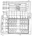
図1は、本発明の実施の形態1に従うTFTアレイ基板の画素回路領域を示す図である。(Embodiment 1)
FIG. 1 is a diagram showing a pixel circuit region of a TFT array substrate according to the first embodiment of the present invention.
図1を参照して、ここでは、画素回路領域は、行列状に配置された複数の画素回路1を含み、一例として、ここでは、n行2m列の行列状に配置された画素回路1について説明する。画素回路のアドレスP(k.l)は、k行目およびl列目の画素回路1を指し示すものとする。本例においては、アドレスP(1.1)、・・・、P(1.2m)、・・・、P(n.2m)が1つずつの画素回路に割り当てられているものとする。 Referring to FIG. 1, here, the pixel circuit region includes a plurality of
なお、ここでは、行に沿って設けられた画素回路1を画素回路行および列に沿って設けられた画素回路1を画素回路列として説明する。 Here, the
本発明の実施の形態1に従う画素回路部は、絶縁基板上に一方向に間隔をおいて配列され、表示する画像に応じた電圧信号を供給するための複数の信号線D1〜D2m+1と、信号線に交差するように他方向に間隔をおいて配列された画素回路1を走査するための複数の走査線G1〜Gn+1とを備える。画素回路1は、複数の信号線のうちの一の信号線と複数の走査線の一の走査線とに対応する位置に配置され、一の走査線の走査信号で選択された際の一の信号線の信号に応じた電流を画素電極に供給する。 The pixel circuit unit according to the first embodiment of the present invention includes a plurality of signal lines D1 to D2m + 1 that are arranged on an insulating substrate at intervals in one direction and supply voltage signals corresponding to an image to be displayed, A plurality of scanning lines G1 to Gn + 1 for scanning the
複数の信号線D1〜D2m+1の各々は、列に沿って設けられ、列に沿って設けられた画素回路の両側にそれぞれ対応して設けられ、かつ隣接する2つの列に沿って設けられた画素回路で共有するように設けられる。また、複数の走査線G1〜Gn+1は、行に沿って設けられた画素回路の両側に一本ずつ設けられ、かつ隣接する2つの行に沿って設けられた画素回路で共有するように設けられる。また、画素回路行にそれぞれ対応して複数の電源供給線VDDが設けられる。なお、後述するが、信号線D2m+1は、検査用の信号線として用いられ、電圧信号は供給されない。 Each of the plurality of signal lines D1 to D2m + 1 is provided along a column, is provided corresponding to both sides of a pixel circuit provided along the column, and is provided along two adjacent columns. Provided to be shared by the circuit. The plurality of scanning lines G1 to Gn + 1 are provided one by one on both sides of the pixel circuit provided along the row, and are provided so as to be shared by the pixel circuits provided along two adjacent rows. . A plurality of power supply lines VDD are provided corresponding to the pixel circuit rows. As will be described later, the signal
ここで、アドレスP(1.1)の画素回路1について具体的構成について説明する。その他の画素回路についても同様である。 Here, a specific configuration of the
画素回路1は、薄膜トランジスタ2,4,6と、保持用キャパシタ3とを備える。なお、ここでは、ここでは、発光表示素子として有機EL素子を用いるものとし、画素回路として、前述した2トランジスタを用いる方式に本発明を適用した場合について説明する。なお、一例として薄膜トランジスタ2(以下、選択用TFT2とも称する)は、NチャネルMOSトランジスタであり、薄膜トランジスタ4(以下、駆動用TFT4とも称する)は、PチャネルMOSトランジスタであり、薄膜トランジスタ6(以下、検査用TFT6とも称する)は、NチャネルMOSトランジスタとする。 The
選択用TFT2は、ドレインが対応する信号線D1と接続され、ソースが保持用キャパシタ3の一端及び駆動用TFT4のゲートと接続され、ゲートが対応する走査線G1と接続される。この対応する行の走査線が活性化されることにより選択TFT2は導通する。 The
保持用キャパシタ3の他端は、電源供給線VDDと接続され、信号線D1から入力される表示する画像に応じた電圧信号を画像信号として保持用キャパシタ3に保持する。 The other end of the holding
駆動用TFT4は、ゲートが保持用キャパシタ3および選択用TFT2のソースと接続され、ソースが電源供給線VDDと接続され、ドレインが有機EL素子7と結合される画素電極5とそれぞれ接続される。 The driving
ここで、画素電極5の上層には、TFTアレイ基板の成型工程の後工程である有機EL成膜工程にて有機EL膜が形成されるが、有機EL成膜工程前のTFTアレイ基板の状態では少なくとも有機EL素子7および画素電極5と反対側の有機EL素子7と結合されるカソード電極8は存在しないので、本例においては、図中において点線で示している。 Here, an organic EL film is formed on the upper layer of the
保持用キャパシタ3に保持される保持電圧は、駆動用TFT4のゲートに印加され、ドレイン側に電流出力経路が形成されたとき、駆動用TFT4は保持電圧に応じた駆動電流を供給する。 The holding voltage held in the holding
本構成においては、この駆動用TFT4から出力される駆動電流を検査するための電流経路を形成するための検査用TFT6が設けられ、そのドレインは画素電極5と接続され、ドレインは隣接する信号線D2と接続され、ゲートは次行の走査線G2とそれぞれ接続される。 In this configuration, an inspection TFT 6 for forming a current path for inspecting a drive current output from the
図2は、本発明の実施の形態1に従うTFTアレイ基板全体の構成を示す図である。
図2を参照して、TFTアレイ基板14は、図1で説明した複数の画素回路が形成される画素回路領域12と、画素回路領域12の周囲に画素回路領域12を囲むようにして設けられ、後述する有機EL素子のカソード電極となるいわゆるITO(Indium Tin Oxide)等で形成される透明電極とTFTアレイ基板との電気的接続をとるためのカソード配線領域13(図中で斜線にて示される)と、第1および第2の端子群10,11とを備える。第1の端子群10は、TFTアレイ基板14の一辺側(本例においては上辺側)に設けられ、各信号線D1,D2,・・・,D2m,D2m+1、電源供給線VDDおよびカソード配線領域13と接続されるカソード配線CATHにそれぞれ対応して設けられ、外部との間で配線接続に用いられる複数の端子を含む。第2の端子群11は、TFTアレイ基板14の他の一辺側(本例においては左辺側)に設けられ、各走査線G1,G2,・・・,Gn+1にそれぞれ対応して設けられ、外部との間で配線接続に用いられる複数の端子を含む。FIG. 2 shows a configuration of the entire TFT array substrate according to the first embodiment of the present invention.
Referring to FIG. 2, the
次に、本発明の実施の形態1に従うTFTアレイ基板14の検査時の動作について説明する。 Next, an operation at the time of inspection of
まず、複数の画素回路のうち、まず奇数列の画素回路を検査し、これらの検査が終了後、偶数列の検査を実行する。奇数列の検査時には、奇数列の信号線D1,D3,・・・,D2m+1に対して信号電圧の印加を行うが、偶数列の信号線D2,D4,・・・,D2mに対しては信号電圧の印加は行わず、電流検出経路として用いる。また、偶数列の検査時には、偶数列の信号線D2,D4,・・・,D2mに対して信号電圧の印加を行うが、奇数列の信号線D1,D3,・・・,D2m+1に対しては信号電圧の印加は行わず、信号線D1,D3,・・・,D2m+1は電流検出経路として用いる。 First, among the plurality of pixel circuits, the odd-numbered pixel circuits are first inspected, and after these inspections are completed, the even-numbered column inspection is executed. At the time of inspection of odd columns, a signal voltage is applied to signal lines D1, D3,..., D2m + 1 of odd columns, but signals are applied to signal lines D2, D4,. The voltage is not applied and used as a current detection path. In the even column inspection, the signal voltage is applied to the even column signal lines D2, D4,..., D2m, but the odd column signal lines D1, D3,. No signal voltage is applied, and the signal lines D1, D3,..., D2m + 1 are used as current detection paths.
ここで、画素回路1の電圧印加時(画素書込み時)と電流出力時における信号線の電位状態について説明する。 Here, the potential state of the signal line at the time of voltage application (pixel writing) and current output of the
図3は、駆動用TFTの特性と有機EL素子の特性とを説明する図である。
上述した図1に示される画素回路1の駆動用TFT4が有機EL素子7に電流を供給するときには、図3に示されるように駆動用TFT4のドレイン電流特性と有機EL素子7の電圧−電流特性から決まる動作点電位が駆動用TFT3のドレイン電位となる。このことから、駆動用TFT3の出力電流を検出する画素検査を行う場合、電流出力時のドレイン電位をこの動作点電位付近に設定して検査することにより、実際の有機EL素子の駆動状態を想定して検査することが可能である。なお、ここでは、駆動用TFT4のソースと接続される電源供給線VDDの電位レベルをVddとして示している。この電位Vddを基点として左側に行くほど駆動用TFT4のドレイン・ソース間電圧およびゲート・ソース間電圧の絶対値が大きくなる。FIG. 3 is a diagram for explaining the characteristics of the driving TFT and the characteristics of the organic EL element.
When the driving
しかしながら、この電位と書込み時に信号線から印加される電位とは必ずしも一致しないため、同じ信号線により電圧の印加と出力電流の検出を行うと、電圧印加時から電流検出時で信号線に電位差(図3に示される左上がりの矢印)が発生することになる。信号線には、多数の走査線や電源供給線が交差しているため配線間容量に伴う寄生容量はかなり大きくなり、2インチクラスの有機EL表示装置で数pF程度にまで達することになる。 However, since this potential does not necessarily match the potential applied from the signal line at the time of writing, if a voltage is applied and the output current is detected by the same signal line, a potential difference (( The upward arrow shown in FIG. 3 is generated. Since a large number of scanning lines and power supply lines intersect with each other in the signal line, the parasitic capacitance accompanying the inter-wiring capacitance is considerably large, and reaches about several pF in a 2-inch class organic EL display device.
一方、有機EL素子を駆動する電流値は有機EL素子の発光効率や要求される表示輝度にも依存するが、同サイズのもので一般的に、1uA以下の微小な電流となる。例えば信号線の寄生容量を5pF、上記の信号線に生じる電位差を2Vとすると、電流出力時に信号線の電位が整定するまでに要する時間を単純に試算すると、20μs程度となる。 On the other hand, the current value for driving the organic EL element depends on the light emission efficiency of the organic EL element and the required display luminance, but is generally the same size and a very small current of 1 uA or less. For example, assuming that the parasitic capacitance of the signal line is 5 pF and the potential difference generated in the signal line is 2 V, the time required until the potential of the signal line is settled at the time of current output is approximately 20 μs.
この場合、外部の電流検出器により検出を開始するまでに、20μs程度の待ち時間を考慮して検出を開始しないと、正確な電流が計測できないことを意味しており、全画素回路を逐次測定する場合には画素回路数分(例えばQuarter VGA(320×240ピクセル)クラスのものでも23万回路)の積算となり、行単位に並列測定できたとしても行数分の積算となり、無視できないレベルとなってくる。 In this case, it means that accurate current cannot be measured unless detection is started in consideration of a waiting time of about 20 μs before detection by an external current detector, and all pixel circuits are sequentially measured. In this case, the integration is performed for the number of pixel circuits (for example, 230,000 circuits for the Quarter VGA (320 × 240 pixels) class). It becomes.
検出器の応答時間なども考慮した時間が1回の検出に要する時間となるが、上記の待ち時間を短縮することは、画素回路の検査の所要時間を短縮する上で極めて重要である。 The time taking into account the response time of the detector is the time required for one detection, but reducing the waiting time is extremely important in reducing the time required for the inspection of the pixel circuit.
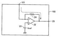
図4は、本発明の実施の形態1に従う電流検出器27の構成を説明する図である。
図4(a)を参照して、本発明の実施の形態1に従う電流検出器27は、入出力端子20a,20bと、電源端子26と、出力端子25と、スイッチ21a,22bと、オペアンプ22と、検出抵抗24と、基準電圧Vrefを供給する電源23とを備える。FIG. 4 is a diagram illustrating a configuration of
Referring to FIG. 4A,
入出力端子20aは、TFTアレイ基板14の奇数列の信号線と電気的に接続され、入出力端子20bは、TFTアレイ基板14の偶数列の信号線と電気的に接続される。スイッチ21aは、選択信号TSの入力に応答して入出力端子20aとノードNa0およびNb0のいずれか一方とを電気的に結合する。スイッチ21bは、選択信号TSの入力に応答して入出力端子20bとノードNa1およびNb1のいずれか一方とを電気的に結合する。 The input /
例えば、奇数列の画素回路を検査する場合、選択信号TSが「H」レベルである場合には、スイッチ21aにおいては、ノードNa0を介して電源端子26と入出力端子20aとを結合する。これにより、電圧源28から電源端子26へ供給された所定電圧Vsが、スイッチ21a、入出力端子20aを経由して奇数列の信号線へ入力される。 For example, when testing pixel circuits in odd columns, if the selection signal TS is at “H” level, the
スイッチ21bにおいては、ノードNa1を介して入出力端子20bとオペアンプ22の反転入力ノードとが結合され、オペアンプ22を用いて偶数列の信号線から出力される駆動用TFTの出力電流を計測する。ここで、オペアンプ22は、その反転入力ノードと出力ノードとの間に検出抵抗24を接続して電流検出器を構成する。 In the
一方、偶数列の画素回路を検査する場合、選択信号TSが「L」レベルである場合には、スイッチ21bにおいては、ノードNb1を介して電源端子26と入出力端子20bとを結合する。これにより、電圧源28から電源端子26へ供給された所定電圧Vsが、スイッチ21b、入出力端子20bを経由して偶数列の信号線へ入力される。 On the other hand, when inspecting the pixel circuits in the even-numbered columns, if the selection signal TS is at the “L” level, the
スイッチ21aにおいては、ノードNb0を介して入出力端子20aとオペアンプ22の反転入力ノードとが結合され、オペアンプ22を用いて奇数列の信号線から出力される駆動用TFTの出力電流を計測する。 In the
検出電流は、I=(Vref−Vout)/Rにより求められる。ここで、Vrefは、オペアンプの非反転入力ノードに印加する基準電圧、Voutは、オペアンプの出力電圧、Rは、検出抵抗24の抵抗値とする。 The detection current is obtained by I = (Vref−Vout) / R. Here, Vref is a reference voltage applied to the non-inverting input node of the operational amplifier, Vout is an output voltage of the operational amplifier, and R is a resistance value of the
この回路では、反転入力ノードと非反転入力ノードとが仮想短絡となり、基準電圧Vrefが反転入力ノードにも現れ、非反転入力ノードからみた入力インピーダンスは、Rin=R/GAとなり、極めて小さい値となる。なお、ここで、GAは、オペアンプ22の開ループゲインとする。すなわち、非反転入力ノードまでの配線抵抗を小さくすれば、駆動用TFT4からの駆動電流が出力される経路となる信号線の電位を基準電圧Vrefに固定することができる。 In this circuit, the inverting input node and the non-inverting input node are virtually short-circuited, the reference voltage Vref appears also at the inverting input node, and the input impedance viewed from the non-inverting input node is Rin = R / GA, which is an extremely small value. Become. Here, GA is an open loop gain of the
これにより、上記の電流検出器を用いることで、駆動電流が流れる検出側の信号線電位の変動が生じない構成とすることができ、電流検出を開始するまでの待ち時間を短縮することが可能となる。 As a result, by using the current detector described above, it is possible to achieve a configuration in which the detection-side signal line potential through which the drive current flows does not fluctuate, and it is possible to shorten the waiting time until current detection is started. It becomes.
なお、ここで、基準電圧Vrefは、有機EL素子の電気的特性が予め判っている場合には、図3において説明した画素回路の駆動用TFT4により電流供給がなされるときの動作点付近の電圧すなわち画素電極の電位近傍に設定するのが望ましい。これは、駆動用TFT4のチャネル長変調やキンク効果の影響により、動作点が移動すると出力される電流も変化するためであり、実際の有機EL素子を駆動する条件を想定して駆動用TFT4の出力電流をより正確に測定するためである。 Here, the reference voltage Vref is a voltage near the operating point when the current is supplied by the driving
図4(b)は、TFTアレイ基板14と、電流検出器27との接続関係を説明する図である。 FIG. 4B is a diagram for explaining the connection relationship between the
図4(b)を参照して、ここでは、TFTアレイ基板14において、電圧供給線VDD、カソード配線CATH、信号線D1〜D2m+1とそれぞれ接続される複数の端子が示されており、それぞれ端子TVDD,TCATH,TD1〜TD2m+1が示されている。そして、信号線D1〜D2m+1にそれぞれ対応する端子TD1〜TD2m+1と駆動用TFT4の駆動電流を測定する電流検出器27が設けられる。具体的には、奇数列および偶数列の信号線にそれぞれ対応する2つずつの端子毎に対応して電流検出器27が設けられ、プローバ(図示せず)により対応する奇数列および偶数列に対応する端子と入出力端子20aと20bとが接続される。同様にして、奇数列および偶数列の信号線D3,D4とそれぞれ接続される端子TD3,TD4に対応して電流検出器27が設けられる。また、信号線D2m−3,D2m−2とそれぞれ接続される端子TD2m−3,TD2m−2に対応して電流検出器27が設けられる。また、信号線D2m−1,D2mとそれぞれ接続される端子TD2m−1,TD2mに対応して電流検出器27が設けられる。また、信号線D2m+1と接続される端子TD2m+1に対応して電流検出器27が設けられ、この場合には、端子TD2m+1は、入出力端子20aと接続され、入出力端子20bはオープン状態とされる。 Referring to FIG. 4B, here, in the
後述するが、例えば、奇数列の画素回路を検査する場合、選択信号TSが「H」レベルである場合には、上述したように電圧源28から電源端子26へ供給された所定電圧Vsが入出力端子20aを経由して奇数列の信号線へ入力される。具体的には、例えば電流検出器27の入出力端子20aから端子TD1に入力され、偶数列の信号線に対応する端子TD2から入出力端子20bに対して駆動用TFTの出力電流が流れて電流検出器27において電流が計測される。同様にして端子TD3,・・・,TD2m−3,TD2m−1,TD2m+1に所定電圧Vsが入力され、端子TD4,・・・,TD2m−2,TD2mから入出力端子20bに対して駆動用TFTの出力電流が流れて電流検出器27において電流が計測される。なお、端子TD2m+1と接続された電流検出器27の入出力端子20bは、オープン状態であるため電流は計測されない。 As will be described later, for example, when the pixel circuits in the odd-numbered columns are inspected, when the selection signal TS is at the “H” level, the predetermined voltage Vs supplied from the
一方、偶数列の画素回路を検査する場合、選択信号TSが「L」レベルである場合には、上述したように電圧源28から電源端子26へ供給された所定電圧Vsが入出力端子20bを経由して偶数列の信号線へ入力される。具体的には、例えば電流検出器27の入出力端子20bから端子TD2に入力される。この場合、後述するが偶数列の信号線に対応する端子TD3から入出力端子20aに対して駆動用TFTの出力電流が流れて電流検出器27において電流が計測される。すなわち、隣接する電流検出器27を用いて電流が計測される。 On the other hand, when the pixel circuits in the even columns are inspected and the selection signal TS is at the “L” level, the predetermined voltage Vs supplied from the
同様にして端子TD4,・・・,TD2m−2,TD2mに所定電圧Vsが入力され、端子TD5(図示せず),・・・,TD2m−1,TD2m+1から入出力端子20aに対して駆動用TFTの出力電流が流れて隣接する電流検出器27において電流が計測される。この場合、端子TD1と接続される電流検出器27において電流は計測されない。 Similarly, the predetermined voltage Vs is inputted to the terminals TD4,..., TD2m-2, TD2m, and the terminal TD5 (not shown),. The output current of the TFT flows and the current is measured by the adjacent
図5は、本発明の実施の形態1に従う画素回路の検査方式について説明する図である。
図5(a)は、奇数列の画素回路に対して検査を実行する場合(奇数列画素の検査)を説明する図である。FIG. 5 is a diagram illustrating a pixel circuit inspection method according to the first embodiment of the present invention.
FIG. 5A is a diagram for explaining a case where inspection is performed on pixel circuits in odd columns (inspection of odd column pixels).
奇数列画素の検査においては、上述したように奇数列の信号線には信号電圧を印加し、奇数列の画素回路の駆動用TFTから出力される電流を隣接する偶数列(本実施の形態では右隣の偶数列として説明する。)の信号線を経由して検出する。 In the inspection of the odd-numbered columns, as described above, a signal voltage is applied to the signal lines in the odd-numbered columns, and the current output from the driving TFTs of the pixel circuits in the odd-numbered columns is applied to the adjacent even-numbered columns (in this embodiment). It will be detected via the signal line of the even-numbered column on the right.
具体的には、選択信号TS(「H」レベル)に従って、電圧源28から電源端子26へ供給された所定電圧Vsが入出力端子20aを経由して奇数列の信号線D1,D3,・・・へ入力される。そして、偶数列の信号線線D2,D4,・・・,D2mを介して入出力端子20bに駆動用TFTの出力電流が流れて電流検出器27において電流が計測される。 Specifically, in accordance with the selection signal TS (“H” level), the predetermined voltage Vs supplied from the
さて、1行目の画素回路1においては、例えば時刻T1において、1行目の画素回路を走査する走査線G1が活性化状態となると、画像信号が奇数列の画素回路に画像信号を供給するための信号線D1,D3,・・・,D2m-1から1行目の画素回路の駆動用TFT4のゲートに印加される。なお、右端の信号線D2m+1は、右端列の画素回路からの検出電流の読出し経路として用いられるのみであるため、画像信号の印加を行わないようにすることも可能である。 In the
このように、信号書込みの画素アドレスとしては、1行目の画素アドレスP(1.1)、P(1.3)、・・・、P(1.2m−1)として示される。ここでは、簡略して画素アドレスP(1.2x−1)と表記されている。 Thus, pixel addresses for signal writing are indicated as pixel addresses P (1.1), P (1.3),..., P (1.2m−1) in the first row. Here, the pixel address P (1.2x−1) is simply described.
時刻T2において、次の2行目の画素回路1を走査すべく走査線G1が非活性レベルとなり走査線G2が活性化レベルとなると、1行目の画素アドレスP(1.2x−1)に対応する画素回路の選択用TFT2が非導通となるが保持用キャパシタ3の保持電圧が駆動用TFT4のゲートに印加され続ける。 At time T2, when the scanning line G1 becomes the inactive level and the scanning line G2 becomes the activation level to scan the
このとき、次行の走査線G2の活性化により1行目の画素アドレスP(1.2x−1)に対応する画素回路の検査用TFT6が導通状態となり、駆動用TFT4からの出力電流が隣接する偶数列の信号線へ出力される。 At this time, the activation of the scanning line G2 in the next row causes the inspection TFT 6 of the pixel circuit corresponding to the pixel address P (1.2x-1) in the first row to be in a conductive state, and the output current from the driving
このときの電流検出器27の出力は同図に示すようになり、時刻T3から検出電流経路の配線容量に充電された電荷が放電するなどして、過渡電流が流れたのち、出力はあるレベルに整定する。このような過渡状態を経過後、図中矢印にて示すような所定のタイミングで電流検出器27の出力をサンプリングしたのち、必要に応じてA/D変換処理を行ってデジタル信号に変換した後、パーソナル・コンピュータなどのコントローラに検出結果として送出する。ここでは、1行目の画素アドレスP(1.2x−1)に対応する画素回路の検出結果が出力される場合が示されている。具体的には、1行目の画素アドレスP(1.1)、P(1.3)、・・・、P(1.2m-1)に対応する画素回路である。 The output of the
このとき、外乱ノイズの影響を除去するために、サンプリング点を複数として平均化処理を行うことも可能である。 At this time, in order to remove the influence of disturbance noise, it is possible to perform averaging processing with a plurality of sampling points.
そして、また、時刻T2において、2行目の画素回路1おいては、2行目の走査線G2が活性化すると画像信号が信号線D1,D3,・・・,D2m−1から2行目の画素回路の駆動用TFT4のゲートに印加される。つまり、信号書込みの画素アドレスは2行目の画素アドレスP(2.1)、P(2.3)、・・・、P(2.2m−1)として示される。ここでは、簡略して画素アドレス(2.2x−1)と表記されている。 At time T2, in the
そして、上記と同様の動作を順次走査線を活性化レベルとして走査しながら、奇数列の先頭の1行目から最終のn行目までの検査を行い、奇数列の画素回路検査が終了する。 Then, the scan from the first row to the last n-th row of the odd-numbered column is performed while sequentially scanning the operation similar to the above with the scanning line as the activation level, and the pixel circuit test of the odd-numbered column is completed.
なお、順次走査線の活性化レベルは操作に従って変化するが、電流検出器27のスイッチ21a,21bは、選択信号TS(「H」レベル)に従って、ノードNa0と入出力端子20aとを電気的に結合し、ノードNa1と入出力端子20bとを電気的に結合した状態を維持し続ける。 Although the activation level of the scanning line sequentially changes according to the operation, the
図5(b)は、偶数列の画素回路に対して検査を実行する場合(偶数列画素の検査)を説明する図である。 FIG. 5B is a diagram illustrating a case where inspection is performed on even-numbered pixel circuits (inspection of even-numbered columns).
偶数列画素の検査においては、上述したように偶数列の信号線には信号電圧を印加し、偶数列の画素回路の駆動用TFTから出力される電流を隣接する奇数列(本実施の形態では右隣の奇数列として説明する。)の信号線を経由して検出する。 In the even column pixel inspection, as described above, a signal voltage is applied to the even column signal line, and the current output from the driving TFT of the pixel circuit of the even column is adjacent to the odd column (in this embodiment). (This will be described as an odd-numbered column on the right.)
具体的には、選択信号TS(「L」レベル)に従って、電圧源28から電源端子26へ供給された所定電圧Vsが入出力端子20bを経由して偶数列の信号線D2,D4,・・・へ入力される。そして、奇数列の信号線線D3,D5,・・・,D2m+1を介して入出力端子20aに駆動用TFTの出力電流が流れて電流検出器27において電流が計測される。なお、左端の奇数列の信号線D1は、奇数列の画素回路に対する検査の際の画像信号の印加経路として用いられるため、偶数列画素の検査の際には、用いられない。すなわち出力電流は流れない。 Specifically, in accordance with the selection signal TS (“L” level), the predetermined voltage Vs supplied from the
さて、1行目の画素回路1においては、例えば時刻T1aにおいて、1行目の画素回路を走査する走査線G1が活性化状態となると、画像信号が偶数列の画素回路に画像信号を供給するための信号線D2,D4,・・・,D2mから1行目の画素回路の駆動用TFT4のゲートに印加される。このように、信号書込みの画素アドレスとしては、簡略して1行目の画素アドレスP(1.2x)と表記されている。 In the
時刻T2aにおいて、次の2行目の画素回路1を走査すべく走査線G1が非活性レベルとなり走査線G2が活性化レベルとなると、1行目の画素アドレスP(1.2x)に対応する画素回路の選択用TFT2が非導通となるが保持用キャパシタ3の保持電圧が駆動用TFT4のゲートに印加され続ける。 At time T2a, when the scanning line G1 becomes inactive level and the scanning line G2 becomes active level to scan the
このとき、次行の走査線G2の活性化により1行目の画素アドレスP(1.2x)に対応する画素回路の検査用TFT6が導通状態となり、駆動用TFT4からの出力電流が隣接する奇数列の信号線へ出力される。 At this time, the activation of the scanning line G2 in the next row causes the inspection TFT 6 of the pixel circuit corresponding to the pixel address P (1.2x) in the first row to be in a conductive state, and the output current from the driving
このときの電流検出器27の出力は同図に示すようになり、時刻T3aから検出電流経路の配線容量に充電された電荷が放電するなどして、過渡電流が流れたのち、出力はあるレベルに整定する。このような過渡状態を経過後、図中矢印にて示すような所定のタイミングで電流検出器27の出力をサンプリングしたのち、必要に応じてA/D変換処理を行ってデジタル信号に変換した後、パーソナル・コンピュータなどのコントローラに検出結果として送出する。ここでは、1行目の画素アドレスP(1.2x)に対応する画素回路の検出結果が出力される場合が示されている。具体的には、1行目の画素アドレスP(1.2)、P(1.4)、・・・、P(1.2m)に対応する画素回路である。 The output of the
そして、上述したように奇数列の画素回路検査と同様に、順次走査線を活性化レベルとして走査しながら、偶数列の先頭の1行目から最終のn行目までの検査を行い、偶数列の画素回路検査が終了する。 Then, as described above, in the same manner as the pixel circuit inspection of the odd-numbered columns, the scanning from the first row to the final n-th row of the even-numbered columns is performed while sequentially scanning the scanning lines as the activation level. This completes the pixel circuit inspection.
そして、コントローラにて、検出電流の検出結果について、所定の閾値レベル以上か否かを判定して、所定の閾値レベル未満であれば画素回路欠陥として判定する。また、全画素回路の電流値のバラツキを算出・判定することにより、より詳細な画素回路の判定を行うことも可能である。さらに、画素回路へ書き込む信号レベルを複数レベルとして検査を行うことも可能である。具体的には、電流検出器の基準電圧を設定することにより検出側の信号線電位を複数レベルとして、画素回路を構成する駆動用TFTの特性をより詳細に検査し確認することも可能である。 Then, the controller determines whether or not the detection result of the detected current is equal to or higher than a predetermined threshold level, and if it is less than the predetermined threshold level, it is determined as a pixel circuit defect. It is also possible to perform more detailed pixel circuit determination by calculating and determining variations in the current values of all pixel circuits. Further, the inspection can be performed with a plurality of signal levels written to the pixel circuit. Specifically, by setting the reference voltage of the current detector, the signal line potential on the detection side can be set to a plurality of levels, and the characteristics of the driving TFT constituting the pixel circuit can be inspected and confirmed in more detail. .
本発明の実施の形態1に従う検査方式は、順次走査線の活性化レベルは操作に従って変化するが、電流検出器27のスイッチ21a,21bは、選択信号TS(「L」レベル)に従って、ノードNa1と入出力端子20aとを電気的に結合し、ノードNa0と入出力端子20bとを電気的に結合した状態を維持し続ける。 In the inspection method according to the first embodiment of the present invention, the activation level of the scanning line sequentially changes according to the operation, but the
すなわち、当該構成においては、偶数列画素の検査および奇数列画素の検査の各々において、画素回路への書込に使用する信号線と、駆動用TFTからの出力電流を検出する経路として使用する信号線とが分離されており、信号線の電位変動が生じない方式となっている。したがって、検出側の信号線電位が固定されるため電位の変動により検出電流の整定時間が長くなることを防止して、検査時間のロスを抑制することが可能である。また、画素回路へ信号を供給する信号線と画素回路からの出力電流を検出する信号線と頻繁に切り替えることなく検査することが可能であり、切り替えに伴う検査時間のロスを防ぐことができる。 That is, in this configuration, in each of the even column pixel inspection and the odd column pixel inspection, a signal line used for writing to the pixel circuit and a signal used as a path for detecting an output current from the driving TFT. The lines are separated from each other, and the signal line does not fluctuate. Therefore, since the signal line potential on the detection side is fixed, it is possible to prevent the settling time of the detection current from becoming long due to the fluctuation of the potential, and it is possible to suppress the inspection time loss. Further, inspection can be performed without frequently switching between a signal line for supplying a signal to the pixel circuit and a signal line for detecting an output current from the pixel circuit, and loss of inspection time due to switching can be prevented.
次に、上記のTFTアレイ基板を用いた表示装置としての有機EL表示パネルを用いた構成について説明する。 Next, a configuration using an organic EL display panel as a display device using the TFT array substrate will be described.
図6は、有機EL表示パネルの構成を説明する図である。
上述したEL成膜工程前のTFTアレイ基板の状態での画素回路検査にて良品と判定され、有機EL成膜工程等を経て有機EL表示パネル30の形態となっているものとする。FIG. 6 is a diagram illustrating the configuration of the organic EL display panel.
Assume that the pixel circuit inspection in the state of the TFT array substrate before the EL film forming process described above is determined as non-defective, and the organic
表示装置を説明する前に、まずTFTアレイ基板を用いた有機EL表示パネル30について説明する。ここでは、EL素子の発光をTFTアレイ基板とは反対側に取り出して表示するトップエミッション構造として説明する。 Before describing the display device, first, an organic
図7は、有機EL表示パネル30の画素部及び端子付近の断面構造図である。
図7を参照して、ガラス等の絶縁基板50上に下地膜51が形成されており、その上にアイランド化された半導体層52が形成されている。半導体層52の上にはゲート絶縁膜53を挟んでゲート電極54が形成されている。半導体層52のソース側にはゲート絶縁膜53や層間絶縁膜57を貫通するコンタクトホール55aが形成され、ソース電極56aと接続されている。なお、半導体層52を用いて形成されたトランジスタは、図1の構成の駆動用TFT4に対応するものである。あるいは、後述する図12で説明する電流プログラム方式の画素回路の場合には、画素電極接続用TFT114に対応するものである。FIG. 7 is a cross-sectional structure diagram in the vicinity of the pixel portion and terminals of the organic
Referring to FIG. 7, a
一方、半導体層52のドレイン側にも同様のコンタクトホール55bが形成され、ドレイン電極56bと接続されている。ドレイン電極56bと同層にあるソース電極56aは保護膜59やさらに上層の平坦化膜60を貫通するコンタクトホール58にて平坦化膜60上層の画素電極61と接続される。保護膜59の上には表面を平坦化するための平坦化膜60が形成されており、その上層に画素電極等が形成される。画素電極61の周縁には画素分離膜62が形成されており、画素分離膜62を形成後に有機EL層63が成膜されている。さらに有機EL層63の上にはITO等の透明電極64が形成され、画素エリア周辺にてカソード配線65と接続がとられる。カソード配線65はソース電極56aやドレイン電極56bと同層にて形成しても良いが、さらにその上層に画素電極61と同層の金属材料を成膜することも可能である。 On the other hand, a
このカソード配線65は、図2で説明した画素回路領域12の周囲に設けられたカソード配線領域13に設けられるものである。TFTアレイ基板側の封止部70は、保護膜57が最上層に形成されており、透明なカバーガラス67の周囲は紫外線硬化樹脂などの封止材68にてTFTアレイ基板と封止されている。 The
再び、図6を参照して、有機EL表示パネル30を構成するTFTアレイ基板の上辺側端子10と接続されるように信号線ドライバIC31(水平ドライバ)が搭載されたTCP36が実装されている。信号線ドライバIC31は、シフトレジスタ回路32、ラッチ回路33、D/A変換回路34、バッファ回路35を含む。 Referring again to FIG. 6, the
また、TFTアレイ基板30の左辺側端子11と接続されるように、走査線ドライバIC37(垂直ドライバ)が搭載されたTCP38が実装されている。 A
次に、表示装置の動作について説明する。
図8は、図6に示される表示装置の動作を説明する図である。Next, the operation of the display device will be described.
FIG. 8 is a diagram for explaining the operation of the display device shown in FIG.
図8を参照して、走査線ドライバIC37に内蔵されたシフトレジスタ回路(図示せず)にはスタートパルスSPV及びシフトクロックCLKVが入力され、順次シフトパルスを発生する。これらの信号に基づいて、走査線を介して画素回路を順次走査する走査信号が生成される。ここでは、時刻T10において、スタートパルスSPVの入力に従って所定周期のシフトクロックCLKVが供給される場合が示されている。 Referring to FIG. 8, a start pulse SPV and a shift clock CLKV are input to a shift register circuit (not shown) built in the scanning
また、信号線ドライバICに内蔵のシフトレジスタ回路32にも同様にスタートパルスSPH及びシフトクロックCLKHが入力され、順次シフトパルスを発生する。このシフトパルスに基づいて、入力されるデジタル画像信号R[5:0]、G[5:0]、B[5:0]がラッチ回路33にてラッチされる。(ここでは、デジタル画像信号は0〜5番目までの各色6ビットの信号として示している。)
そして、ラッチ回路33にてラッチされた1行の表示に対応する信号に線順次化されたデジタル画像信号は、D/A変換回路34にてアナログ信号に変換され、バッファ回路35を介して各列の信号線D1,D2,・・・,D2m-1,D2mに供給される。ここでは、時刻T10に第1行目の走査線G1が活性化されて第1行目の画素回路に対して書込みが実行され、時刻T11に第2行目の走査線G2が活性化されて第2行目の画素回路に対して書込みが実行される。以下、同様にして、昇順的に順次上述したように走査線が活性化されて書込みが実行される。Similarly, the start pulse SPH and the shift clock CLKH are similarly input to the
Then, the digital image signal line-sequentially converted into a signal corresponding to the display of one row latched by the
このとき前述したように、各画素回路1においては、対応する信号線からの電圧信号に応じて駆動用TFTから駆動電流が出力される。ここで、画素電極に電気的に接続された検査用TFTのゲートを次ラインの走査線に接続した構成としているので、当該走査線が活性化されて、書込みが終了した後、次のラインの走査線が活性化して対応する画素回路への書込みを実行する際に、前のラインの検査用TFTが導通することになる。このため駆動用TFTからの駆動電流は隣接する信号線を介して、有機EL素子よりも出力インピーダンスの低いバッファ回路へと分流することになる。そのため書込みが完了した後、次ラインの書込み期間は有機EL発光素子への電流が低下する。例えば時刻T10に第1行目の走査線G1を活性化させて第1行目の画素回路に対して書込みを実行した後、時刻T11に第2行目の走査線G2を活性化させた場合、第1行目の画素回路の検査用TFTが導通することになるので、時刻T11から第1行目の画素回路の有機EL発光素子に対して流れる電流が低下することになる。 At this time, as described above, in each
しかしながら、次ラインの走査が終了後、さらに次の次次ラインの走査に移ると、次ライン走査線は非活性となり、検査用TFTは非導通となるので、隣接信号線への分流経路は遮断される。具体的には、例えば時刻T11に第2行目の走査線G2を活性化させた後、時刻T12に第3行目の走査線G3を活性化させた場合、第2行目の走査線G2は被活性化状態に設定される。したがって、時刻T12において、第1行目の画素回路の検査用TFTは非導通状態に設定され、駆動用TFTの出力電流は再び有機EL発光素子に対して流れ、所定の発光強度にて発光し、所望の画面表示が行われる。 However, when the next line scan is completed after the next line scan is completed, the next line scan line becomes inactive and the inspection TFT becomes non-conductive, so that the shunt path to the adjacent signal line is cut off. Is done. Specifically, for example, when the second scanning line G2 is activated at time T12 and then the third scanning line G3 is activated at time T12, the second scanning line G2 is activated. Is set to the activated state. Therefore, at time T12, the inspection TFT of the pixel circuit in the first row is set to a non-conductive state, and the output current of the driving TFT flows again to the organic EL light emitting element, and emits light with a predetermined light emission intensity. A desired screen display is performed.
したがって、書込みが終了してから次ライン走査期間中、有機EL発光素子への電流が低下するため発光強度が低下するが、フレーム期間に比べ極めて短期間であり、電流が低下することによる画面表示への影響は殆どないものと考えられる。 Therefore, during the next line scanning period after the writing is completed, the current to the organic EL light emitting element is reduced, so that the light emission intensity is reduced. However, the screen display is extremely short compared to the frame period, and the current is reduced. It is considered that there is almost no impact on
(実施の形態2)
本発明の実施の形態2に従う構成においては、水平ドライバ回路及び走査線ドライバ回路をTFTアレイ基板に内蔵する形態について説明する。(Embodiment 2)
In the configuration according to the second embodiment of the present invention, a mode in which the horizontal driver circuit and the scanning line driver circuit are built in the TFT array substrate will be described.
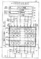
図9は本発明の実施の形態2に従うTFTアレイ基板の構成を説明する図である。
図9を参照して、TFTアレイ基板80には例えば低温ポリシリコンTFTを用いて水平ドライバ回路81及び走査線ドライバ回路89が構成されており、例えば画素回路領域12の上辺側に水平ドライバ回路81を、左辺側に走査線ドライバ回路89が配置される。FIG. 9 is a diagram illustrating a configuration of a TFT array substrate according to the second embodiment of the present invention.
Referring to FIG. 9, a
水平ドライバ回路81は、実施の形態1における有機EL表示パネルの構成として説明したのと同様に、シフトレジスタ回路82、ラッチ回路83、D/A変換回路84、バッファ回路85とで構成されている。 The
また、水平ドライバ回路81と画素回路領域12との間には、水平ドライバ回路81の出力信号の各信号線への供給を制御する出力制御回路86が設けられる。 Further, an
出力制御回路86は、一端が水平ドライバ回路81の出力端と接続され、他端が画素回路領域12に設けられる奇数列及び偶数列の信号線にそれぞれ接続されたスイッチ回路87及び88を含む。本例においては、一例として奇数列の信号線D1,D3,・・・D2m−1の信号線に対応してスイッチ回路87が設けられ、偶数列の信号線D2,D4,・・・,D2mの信号線に対応してスイッチ回路88が設けられて、水平ドライバ回路81から画素回路領域12への出力信号の供給が制御される。 The
奇数列の信号線に接続されたスイッチ回路87は、出力イネーブル信号OEoが活性化したときに導通し、また偶数列の信号線に接続されたスイッチ回路88は出力イネーブル信号OEeが活性化したときに導通する。ここで、右端の信号線D2m+1は、実施の形態1の構成で説明したように検査時において、右端列の画素回路1からの読出電流を検出する経路を構成するのみで、信号の印加には使用されないため、スイッチ回路87を接続する必要は無いためここでは、記載されていないがレイアウトパターンの均一性を確保する観点から設けることも可能である。 The
TFTアレイ基板80の端部である画素回路領域12の上辺側には信号入力用端子90が配置され、水平ドライバ回路81及び走査線ドライバ回路89を制御する制御信号やデジタル画像信号R[5:0],G[5:0],B[5:0]、出力制御回路86を制御する出力イネーブル信号OEo、OEeを供給する配線、及び各画素回路1に接続された電源供給線VDDやカソード配線CATHは信号入力用端子90と接続されて外部から信号および電圧の供給が実行されるものとする。 A
また、TFTアレイ基板80の端部である画素回路領域12の下辺側には検査用回路91が内蔵されるとともに複数の検査用端子94が配置されている。検査用端子94は、TFTアレイ基板80の端部において検査用回路91と接続され、検査用回路91を制御するとともに、検査用回路91を介して流れる電流を外部に供給する。 In addition, an
具体的に説明すると、検査用回路91は、偶数列の信号線である信号線D2,D4,・・・,D2mに一端が接続され、他端が検査用端子94に接続されたスイッチ回路92と、奇数列の信号線D3,D5,・・・,D2m+1に一端が接続され、他端が検査用端子94に接続されたスイッチ回路93とを含む。 More specifically, the
スイッチ回路92は、検査用端子94を介して外部から入力されるセレクト信号SELoに応答して導通し、スイッチ回路93は、検査用端子94を介して外部から入力されるセレクト信号SELeに応答して導通する。例えば、セレクト信号SELo,SELeが「H」レベルに設定された場合に、スイッチ回路92,93が導通し、「L」レベルに設定された場合にスイッチ回路92,93が非導通状態に設定されるものとする。 The
図10は、TFTアレイ基板80の検査用端子94と接続される電流検出器100の構成を説明する図である。 FIG. 10 is a diagram for explaining the configuration of the
図10を参照して、本発明の実施の形態2に従う電流検出器100は、電流検出器27と比較して、スイッチ21a,22bと、入出力端子20a,20bと、電源端子26とが削除され、新たに入力端子101が設けられた構成である。 Referring to FIG. 10, in
具体的には、電流検出器100は、入力端子101と、出力端子25と、オペアンプ22と、検出抵抗24と、基準電圧Vrefを供給する電源23とを備える。 Specifically, the
入力端子101は、検査用端子94と接続されてスイッチ92,93のいずれか一方を介して奇数列あるいは偶数列に対応する信号線に流れる電流の供給を受ける。 The
例えば、入力端子101は、上述したようにセレクト信号SELoが「H」レベルに設定された場合には、スイッチ92が導通して、奇数列に対応する信号線からの電流の供給を受ける。一方、セレクト信号SELeが「H」レベルに設定された場合には、スイッチ93が導通して、偶数列に対応する信号線からの電流の供給を受ける。 For example, when the select signal SELo is set to the “H” level as described above, the
そして、図4で説明したのと同様に上述したようにオペアンプ22を用いて偶数列あるいは奇数列の信号線からの出力電流が計測される。ここで、オペアンプ22は、その反転入力ノードと出力ノードとの間に検出抵抗24を接続して電流検出器を構成する。 As described above with reference to FIG. 4, the output current from the signal lines in the even-numbered columns or odd-numbered columns is measured using the
次に、TFTアレイ基板状態での検査における動作を説明する。
図11は、本発明の実施の形態2に従う画素回路の検査方式について説明する図である。Next, the operation in the inspection in the TFT array substrate state will be described.
FIG. 11 is a diagram illustrating a pixel circuit inspection method according to the second embodiment of the present invention.
図11(a)は、奇数列の画素回路に対して検査を実行する場合(奇数列画素の検査)を説明する図である。 FIG. 11A is a diagram illustrating a case where inspection is performed on pixel circuits in odd columns (inspection of odd column pixels).
奇数列画素の検査においては、上述したように奇数列の信号線には信号電圧を印加し、奇数列の画素回路の駆動用TFTから出力される電流を隣接する偶数列(本実施の形態では右隣の偶数列として説明する。)の信号線を経由して検出する。 In the inspection of the odd-numbered column pixels, as described above, a signal voltage is applied to the odd-numbered column signal line, and the current output from the driving TFT of the odd-numbered pixel circuit is supplied to the adjacent even-numbered column (in this embodiment). It will be detected via the signal line of the even-numbered column on the right.
具体的には、上述したように水平ドライバ回路81を構成するシフトレジスタ回路82にスタートパルスSPH及びシフトクロックCLKHが入力され、順次シフトパルスが上述したように生成される。このシフトパルスに基づいて、入力されるデジタル画像信号R[5:0],G[5:0],B[5:0]がラッチ回路83にてラッチされる。(ここでは、デジタル画像信号は各色6ビットの信号として示している。)
そして、ラッチ回路83において、ラッチされ、1行の表示に対応する信号に線順次化されたデジタル画像信号がD/A変換回路84にてアナログ信号に変換され、バッファ回路85を介して水平ドライバ回路81から出力される。Specifically, the start pulse SPH and the shift clock CLKH are input to the
The digital image signal latched in the
また、上述したように走査線ドライバ回路89に内蔵されたシフトレジスタ回路(図示せず)にはスタートパルスSPV及びシフトクロックCLKVが入力され、順次シフトパルスを発生し、これらをもとに、走査線を介して画素回路を順次走査する走査信号を生成する。 Further, as described above, the start pulse SPV and the shift clock CLKV are input to the shift register circuit (not shown) built in the scanning
そして、本発明の実施の形態2に従う構成においては、奇数列の画素回路を検査する場合、出力イネーブル信号OEoが活性化状態となり、また出力イネーブル信号OEeは非活性状態となる。これに応答して、スイッチ回路87が導通し、スイッチ回路88は非導通状態となる。それゆえ、奇数列の信号線D1,D3,・・・,D2m-1には水平ドライバ回路81から出力される所定の電圧が印加される。また、偶数列の信号線D2,D4,・・・,D2mはスイッチ88を介して水平ドライバ回路81から切り離されている。 In the configuration according to the second embodiment of the present invention, when the pixel circuits in the odd-numbered columns are inspected, the output enable signal OEo is activated and the output enable signal OEe is deactivated. In response to this, the
一方、セレクト信号SELeは、活性化状態となり、検査用回路91のスイッチ回路93が導通状態となり偶数列D2,D4,・・・,D2mが検査用端子94を介して上述した電流検出器100とそれぞれ電気的に接続された状態となる。また、セレクト信号SELoは非活性状態であり、奇数列の信号線D1,D3,・・・,D2m+1は検査用端子94と切り離されている。本例においては、時刻T0bに出力イネーブル信号OEoおよびセレクト信号SELeが活性化状態とされ、出力イネーブル信号OEeおよびセレクト信号SELoが非活性化状態とされた場合が示されている。 On the other hand, the select signal SELe is activated, the
さて、1行目の画素回路1においては、例えば時刻T1bにおいて、1行目の画素回路を走査する走査線G1が活性化状態となると、画像信号が奇数列の画素回路に画像信号を供給するための信号線D1,D3,・・・,D2m-1から1行目の画素回路の駆動用TFT4のゲートに印加される。なお、右端の信号線D2m+1は、右端列の画素回路からの検出電流の読出し経路として用いられるのみであるため、画像信号の印加は行われない構成となっている。 In the
このように、信号書込みの画素アドレスとしては、1行目の画素アドレスP(1.1)、P(1.3)、・・・、P(1.2m−1)として示される。ここでは、簡略して画素アドレスP(1.2x−1)と表記されている。 Thus, pixel addresses for signal writing are indicated as pixel addresses P (1.1), P (1.3),..., P (1.2m−1) in the first row. Here, the pixel address P (1.2x−1) is simply described.
時刻T2bにおいて、次の2行目の画素回路1を走査すべく走査線G1が非活性レベルとなり走査線G2が活性化レベルとなると、1行目の画素アドレスP(1.2x−1)に対応する画素回路の選択用TFT2が非導通となるが保持用キャパシタ3の保持電圧が駆動用TFT4のゲートに印加され続ける。 At time T2b, when the scanning line G1 is inactivated and the scanning line G2 is activated to scan the
このとき、次行の走査線G2の活性化により1行目の画素アドレスP(1.2x−1)に対応する画素回路の検査用TFT6が導通状態となり、駆動用TFT4からの出力電流が隣接する偶数列の信号線へ出力される。 At this time, the activation of the scanning line G2 in the next row causes the inspection TFT 6 of the pixel circuit corresponding to the pixel address P (1.2x-1) in the first row to be in a conductive state, and the output current from the driving
このときの電流検出器100の出力は同図に示すようになり、時刻T3bから検出電流経路の配線容量に充電された電荷が放電するなどして、過渡電流が流れたのち、出力はあるレベルに整定する。このような過渡状態を経過後、図中矢印にて示すような所定のタイミングで電流検出器100の出力をサンプリングしたのち、必要に応じてA/D変換処理を行ってデジタル信号に変換した後、パーソナル・コンピュータなどのコントローラに検出結果として送出する。ここでは、1行目の画素アドレスP(1.2x−1)に対応する画素回路の検出結果が出力される場合が示されている。具体的には、1行目の画素アドレスP(1.1)、P(1.3)、・・・、P(1.2m-1)に対応する画素回路である。 The output of the
このとき、外乱ノイズの影響を除去するために、サンプリング点を複数として平均化処理を行うことも可能である。 At this time, in order to remove the influence of disturbance noise, it is possible to perform averaging processing with a plurality of sampling points.
そして、また、時刻T2bにおいて、2行目の画素回路1おいては、2行目の走査線G2が活性化すると画像信号が信号線D1,D3,・・・,D2m−1から2行目の画素回路の駆動用TFT4のゲートに印加される。つまり、信号書込みの画素アドレスは2行目の画素アドレスP(2.1)、P(2.3)、・・・、P(2.2m−1)として示される。ここでは、簡略して画素アドレス(2.2x−1)と表記されている。 At time T2b, in the
そして、上記と同様の動作を順次走査線を活性化レベルとして走査しながら、奇数列の先頭の1行目から最終のn行目までの検査を行い、奇数列の画素回路検査が終了する。 Then, the scan from the first row to the last n-th row of the odd-numbered column is performed while sequentially scanning the operation similar to the above with the scanning line as the activation level, and the pixel circuit test of the odd-numbered column is completed.
図11(b)は、偶数列の画素回路に対して検査を実行する場合(偶数列画素の検査)を説明する図である。 FIG. 11B is a diagram illustrating a case where inspection is performed on even-numbered pixel circuits (inspection of even-numbered columns).
偶数列画素の検査においては、上述したように偶数列の信号線には信号電圧を印加し、偶数列の画素回路の駆動用TFTから出力される電流を隣接する奇数列(本実施の形態では右隣の奇数列として説明する。)の信号線を経由して検出する。 In the even column pixel inspection, as described above, a signal voltage is applied to the even column signal line, and the current output from the driving TFT of the pixel circuit of the even column is adjacent to the odd column (in this embodiment). (This will be described as an odd-numbered column on the right.)
具体的には、上述したように水平ドライバ回路81を構成するシフトレジスタ回路82にスタートパルスSPH及びシフトクロックCLKHが入力され、順次シフトパルスが上述したように生成される。このシフトパルスに基づいて、入力されるデジタル画像信号R[5:0],G[5:0],B[5:0]がラッチ回路83にてラッチされる。(ここでは、デジタル画像信号は各色6ビットの信号として示している。)
そして、ラッチ回路83において、ラッチされ、1行の表示に対応する信号に線順次化されたデジタル画像信号がD/A変換回路84にてアナログ信号に変換され、バッファ回路85を介して水平ドライバ回路81から出力される。Specifically, the start pulse SPH and the shift clock CLKH are input to the
The digital image signal latched in the
また、上述したように走査線ドライバ回路89に内蔵されたシフトレジスタ回路(図示せず)にはスタートパルスSPV及びシフトクロックCLKVが入力され、順次シフトパルスを発生し、これらをもとに、走査線を介して画素回路を順次走査する走査信号を生成する。 Further, as described above, the start pulse SPV and the shift clock CLKV are input to the shift register circuit (not shown) built in the scanning
そして、本発明の実施の形態2に従う構成においては、偶数列の画素回路を検査する場合、出力イネーブル信号OEeが非活性化状態となり、また出力イネーブル信号OEoは活性状態となる。これに応答して、スイッチ回路88が導通し、スイッチ回路87は非導通状態となる。それゆえ、偶数列の信号線D2,D4,・・・,D2mには水平ドライバ回路81から出力される所定の電圧が印加される。また、奇数列の信号線D1,D3,D5,・・・,D2m−1はスイッチ87を介して水平ドライバ回路81から切り離されている。 In the configuration according to the second embodiment of the present invention, when inspecting even-numbered pixel circuits, the output enable signal OEe is deactivated and the output enable signal OEo is activated. In response to this, the
一方、セレクト信号SELoは、活性化状態となり、検査用回路91のスイッチ回路92が導通状態となり偶数列D3,D5,・・・,D2m+1が検査用端子94を介して上述した電流検出器100とそれぞれ電気的に接続された状態となる。また、セレクト信号SELeは非活性状態であり、偶数列の信号線D2,D4,・・・,D2mは検査用端子94と切り離されている。本例においては、時刻T0cに出力イネーブル信号OEeおよびセレクト信号SELoが活性化状態とされ、出力イネーブル信号OEoおよびセレクト信号SELeが非活性化状態とされた場合が示されている。 On the other hand, the select signal SELo is activated, the
さて、1行目の画素回路1においては、例えば時刻T1cにおいて、1行目の画素回路を走査する走査線G1が活性化状態となると、画像信号が偶数列の画素回路に画像信号を供給するための信号線D2,D4,・・・,D2mから1行目の画素回路の駆動用TFT4のゲートに印加される。このように、信号書込みの画素アドレスとしては、簡略して1行目の画素アドレスP(1.2x)と表記されている。 In the
時刻T2cにおいて、次の2行目の画素回路1を走査すべく走査線G1が非活性レベルとなり走査線G2が活性化レベルとなると、1行目の画素アドレスP(1.2x)に対応する画素回路の選択用TFT2が非導通となるが保持用キャパシタ3の保持電圧が駆動用TFT4のゲートに印加され続ける。 At time T2c, when the scanning line G1 becomes inactive level and the scanning line G2 becomes active level to scan the
このとき、次行の走査線G2の活性化により1行目の画素アドレスP(1.2x)に対応する画素回路の検査用TFT6が導通状態となり、駆動用TFT4からの出力電流が隣接する奇数列の信号線へ出力される。 At this time, the activation of the scanning line G2 in the next row causes the inspection TFT 6 of the pixel circuit corresponding to the pixel address P (1.2x) in the first row to be in a conductive state, and the output current from the driving
このときの電流検出器100の出力は同図に示すようになり、時刻T3cから検出電流経路の配線容量に充電された電荷が放電するなどして、過渡電流が流れたのち、出力はあるレベルに整定する。このような過渡状態を経過後、図中矢印にて示すような所定のタイミングで電流検出器100の出力をサンプリングしたのち、必要に応じてA/D変換処理を行ってデジタル信号に変換した後、パーソナル・コンピュータなどのコントローラに検出結果として送出する。ここでは、1行目の画素アドレスP(1.2x)に対応する画素回路の検出結果が出力される場合が示されている。具体的には、1行目の画素アドレスP(1.2)、P(1.4)、・・・、P(1.2m)に対応する画素回路である。 The output of the
そして、上述したように奇数列の画素回路検査と同様に、順次走査線を活性化レベルとして走査しながら、偶数列の先頭の1行目から最終のn行目までの検査を行い、偶数列の画素回路検査が終了する。 Then, as described above, in the same manner as the pixel circuit inspection of the odd-numbered columns, the scanning from the first row to the final n-th row of the even-numbered columns is performed while sequentially scanning the scanning lines as the activation level. This completes the pixel circuit inspection.
そして、実施の形態1で説明したのと同様、コントローラにて、検出電流の検出結果について、所定の閾値レベル以上か否かを判定して、所定の閾値レベル未満であれば画素回路欠陥として判定する。また、全画素回路の電流値のバラツキを算出・判定することにより、より詳細な画素回路の判定を行うことも可能である。さらに、画素回路へ書き込む信号レベルを複数レベルとして検査を行うことも可能である。具体的には、電流検出器の基準電圧を設定することにより検出側の信号線電位を複数レベルとして、画素回路を構成する駆動用TFTの特性をより詳細に検査し確認することも可能である。 Then, as described in the first embodiment, the controller determines whether or not the detection result of the detected current is equal to or higher than a predetermined threshold level, and if it is less than the predetermined threshold level, it is determined as a pixel circuit defect. To do. It is also possible to perform more detailed pixel circuit determination by calculating and determining variations in the current values of all pixel circuits. Further, the inspection can be performed with a plurality of signal levels written to the pixel circuit. Specifically, by setting the reference voltage of the current detector, the signal line potential on the detection side can be set to a plurality of levels, and the characteristics of the driving TFT constituting the pixel circuit can be inspected and confirmed in more detail. .
当該構成のTFTアレイ基板に対して、実施の形態1の図7で説明したようなEL成膜工程等を経た構造にて有機EL表示パネルとなった場合においても実施の形態1と同様の表示動作により所望の画像表示が行われる。 Even when an organic EL display panel is formed on the TFT array substrate having such a structure through the EL film forming process and the like described in FIG. 7 of the first embodiment, the same display as in the first embodiment is performed. A desired image display is performed by the operation.
なお、実施の形態1および2に従う構成においては、図17(a)に示した2トランジスタ型の画素回路に対して検査用TFTを用いた構成について説明したが、図17(b)に示した電圧プログラム型のような電圧書込み型の画素回路についても同様に適用可能である。 In the configuration according to the first and second embodiments, the configuration in which the inspection TFT is used for the two-transistor pixel circuit illustrated in FIG. 17A has been described. However, the configuration illustrated in FIG. The present invention can be similarly applied to a voltage writing type pixel circuit such as a voltage program type.
なお、有機EL成膜工程等を経て有機EL表示パネルすなわち表示装置となった後、表示領域の下辺封止領域の外側にて切断することが本構成においては可能である。具体的には、図9で示されるようにK−Kの箇所(二点鎖線で示す)で切断することにより、検査用回路や検査用端子を切り落としてしまうことにより、有機EL表示パネルである表示装置の最終形態においては不要なこれらを切断することにより額縁領域が広がることを防止し、小型化することが可能である。 In this configuration, after the organic EL display panel, that is, the display device is obtained through the organic EL film forming process and the like, cutting is performed outside the lower side sealing region of the display region. Specifically, as shown in FIG. 9, an organic EL display panel is obtained by cutting off a test circuit and a test terminal by cutting at a position KK (shown by a two-dot chain line). In the final form of the display device, it is possible to prevent the frame area from expanding by cutting these unnecessary parts and to reduce the size.
(実施の形態3)
本発明の実施の形態3においては、電流書込型の画素回路について、図17(d)に示した電流プログラム方式を使用したTFTアレイ基板とその検査方法について説明する。(Embodiment 3)
In the third embodiment of the present invention, a TFT array substrate using the current programming method shown in FIG. 17D and an inspection method thereof will be described for a current writing type pixel circuit.
図12は、本発明の実施の形態3に従うTFTアレイ基板の画素回路領域を示す図である。 FIG. 12 shows a pixel circuit region of the TFT array substrate according to the third embodiment of the present invention.
図12を参照して、ここでは、画素回路領域は、行列状に配置された複数の画素回路110を含み、一例として、ここでは、n行2m列の行列状に配置された画素回路110について説明する。画素回路のアドレスP(k.l)は、k行目およびl列目の画素回路110を指し示すものとする。本例においては、アドレスP(1.1)、・・・、P(1.2m)、・・・、P(n.2m)が1つずつの画素回路に割り当てられているものとする。 Referring to FIG. 12, here, the pixel circuit region includes a plurality of
なお、ここでは、行に沿って設けられた画素回路110を画素回路行および列に沿って設けられた画素回路110を画素回路列として説明する。 Here, the
本発明の実施の形態1に従う画素回路領域は、表示する画像に応じた電圧信号を供給するための複数の信号線D1〜D2m+1と、画素回路110を走査するための複数の走査線G1a,G1b〜Gna,Gnbとを備える。複数の信号線D1〜D2m+1の各々は、列に沿って設けられ、列に沿って設けられた画素回路の両側にそれぞれ対応して設けられ、かつ隣接する2つの列に沿って設けられた画素回路で共有するように設けられる。また、複数の走査線G1a,G1b〜Gna,Gnbは、行に沿って設けられた画素回路にそれぞれ対応して2本ずつ設けられ、それぞれ対応する画素回路を挟むようにして一方側および他方側に設けられる。また、画素回路行にそれぞれ対応して複数の電源供給線VDDが設けられる。なお、上述したように信号線D2m+1は、検査用の信号線として用いられ、電圧信号は供給されない。なお、走査線G1b,G2b,Gnbは、他の走査線に並行するように配設され、検査用のために駆動される走査線(テスト信号線)であり、通常の表示時には駆動されないものである。 The pixel circuit area according to the first embodiment of the present invention includes a plurality of signal lines D1 to D2m + 1 for supplying a voltage signal corresponding to an image to be displayed and a plurality of scanning lines G1a and G1b for scanning the
ここで、アドレスP(1.1)の画素回路110について具体的構成について説明する。その他の画素回路についても同様である。 Here, a specific configuration of the
画素回路110は、薄膜トランジスタ111〜117と、保持用キャパシタ113とを備える。なお、ここでは、ここでは、発光表示素子として有機EL素子を用いるものとし、画素回路として、図17(d)に示した電流プログラム型画素回路に対して、検査用TFT117が付加された構成となっている。 The
なお、一例として薄膜トランジスタ111(以下、選択用TFT111とも称する)および薄膜トランジスタ112(以下、ダイオード接続用TFT112とも称する)は、NチャネルMOSトランジスタであり、薄膜トランジスタ113(以下、駆動用TFT113とも称する)および薄膜トランジスタ114(以下、画素電極接続用TFT114とも称する)は、PチャネルMOSトランジスタであり、薄膜トランジスタ117(以下、検査用TFT117とも称する)は、NチャネルMOSトランジスタとする。 As an example, the thin film transistor 111 (hereinafter also referred to as a selection TFT 111) and the thin film transistor 112 (hereinafter also referred to as a diode connection TFT 112) are N-channel MOS transistors, and the thin film transistor 113 (hereinafter also referred to as a driving TFT 113) and the thin film transistor. 114 (hereinafter also referred to as pixel electrode connecting TFT 114) is a P-channel MOS transistor, and thin film transistor 117 (hereinafter also referred to as inspection TFT 117) is an N-channel MOS transistor.
選択用TFT111のソースは、対応する信号線D1と接続され、ゲートは走査線G1aと接続される。また、ドレインは駆動用TFT113および画素電極接続用TFT114の接続ノードNtと接続される。また、ダイオード接続用TFT112のソースは、接続ノードNtと接続され、ドレインが保持用キャパシタ115の一端および駆動用TFT113のゲートと接続され、ゲートが対応する走査線G1aと接続される。保持用キャパシタ115は、一端が駆動用TFT113のゲートおよびダイオード接続用TFT112のドレインと接続される。他端が電源電圧VDDの供給を受ける電源線と接続される。 The source of the
駆動用TFT113は、ソースが電源電圧VDDの供給を受ける電源線と接続され、ドレインがノードNtと接続され、ゲートがキャパシタ115の一端およびダイオード接続用TFT112のドレインと接続される。画素電極接続用TFT114は、ソースが接続ノードNtと接続され、ドレインが画素電極116と接続され、ゲートは走査線G1aと接続される。そして、検査用TFT117は、ドレインが画素電極116と接続され、ゲートは走査線G1bと接続され、ソースが隣接する信号線(右隣)と接続される。 The driving
なお、画素電極116の上層にはTFTアレイ工程の後工程である有機EL成膜工程にて有機EL膜が形成されるが、有機EL成膜工程前のTFTアレイ基板の状態では少なくとも有機EL素子7やカソード電極8は存在しないので、図中には点線で示している。 An organic EL film is formed on the
保持用キャパシタ115に保持される保持電圧は、駆動用TFT113のゲートに印加され、ドレイン側に電流出力経路が形成されたとき、駆動用TFT113は、保持電圧に応じた駆動電流を供給する。 The holding voltage held in the holding
本構成においては、この駆動用TFT113から出力される駆動電流を検査するための電流経路を形成するための検査用TFT117が設けられ、そのドレインは画素電極116と接続され、ソースは隣接する信号線D2と接続され、ゲートは走査線G1bと接続される。 In this configuration, an
なお、TFTアレイ基板は、実施の形態1の図2で説明した構成と同様である。具体的には、画素回路1を画素回路110に置換した構成である。図2の構成においては、走査線G1〜Gn+1にそれぞれ対応して第2の端子群11が設けられる構成について説明したが、本発明の実施の形態3に従う構成は、G1a,G1b〜Gna,Gnbにそれぞれ対応して第2の端子群11が設けられる点が異なる。その他の点については、同様であるのでその詳細な説明は繰り返さない。 Note that the TFT array substrate has the same configuration as that described in FIG. 2 of the first embodiment. Specifically, the
また、実施の形態1の図4で説明した電流検出器を用いることにより画素回路の検査を実行することができる。 In addition, the pixel circuit can be inspected by using the current detector described in FIG. 4 of the first embodiment.
図13は、本発明の実施の形態3に従う画素回路の検査方式について説明する図である。 FIG. 13 is a diagram illustrating a pixel circuit inspection method according to the third embodiment of the present invention.
図13(a)は、奇数列の画素回路に対して検査を実行する場合(奇数列画素の検査)を説明する図である。 FIG. 13A is a diagram illustrating a case where inspection is performed on pixel circuits in odd columns (inspection of odd column pixels).
奇数列画素の検査においては、上述したように奇数列の信号線には信号電圧を印加し、奇数列の画素回路の駆動用TFTから出力される電流を隣接する偶数列(本実施の形態では右隣の偶数列として説明する。)の信号線を経由して検出する。 In the inspection of the odd-numbered columns, as described above, a signal voltage is applied to the signal lines in the odd-numbered columns, and the current output from the driving TFTs of the pixel circuits in the odd-numbered columns is applied to the adjacent even-numbered columns (in this embodiment). It will be detected via the signal line of the even-numbered column on the right.
具体的には、上述したように選択信号TS(「H」レベル)に従って、電圧源28から電源端子26へ供給された所定電圧Vsが入出力端子20aを経由して奇数列の信号線D1,D3,・・・へ入力される。そして、偶数列の信号線線D2,D4,・・・,D2mを介して入出力端子20bに駆動用TFTの出力電流が流れて電流検出器27において電流が計測される。 Specifically, as described above, in accordance with the selection signal TS (“H” level), the predetermined voltage Vs supplied from the
さて、1行目の画素回路110においては、例えば時刻T1dにおいて、1行目の画素回路を走査する走査線G1aが活性化状態となると、ダイオード接続用TFT112が導通し、駆動用TFT113のゲート−ドレイン間が接続されてダイオード接続状態となる。また、走査線G1aが活性化状態となると、選択用TFT111が導通するため対応する信号線からダイオード接続状態となった駆動用TFT113のソース−ドレイン間に電流が流れ、ゲート電圧が保持用キャパシタ115に保持される。一方、画素電極接続用TFT114は非導通状態である。画像信号が奇数列の画素回路に画像信号を供給するための信号線D1,D3,・・・,D2m-1から1行目の画素回路の駆動用TFT113のゲートに印加される。なお、右端の信号線D2m+1は、右端列の画素回路からの検出電流の読出し経路として用いられるのみであるため、画像信号の印加を行わないようにすることも可能である。 In the
このように、信号書込みの画素アドレスとしては、1行目の画素アドレスP(1.1),P(1.3),・・・、P(1.2m−1)として示される。ここでは、簡略して画素アドレスP(1.2x−1)と表記されている。 Thus, pixel addresses for signal writing are indicated as pixel addresses P (1.1), P (1.3),..., P (1.2m−1) in the first row. Here, the pixel address P (1.2x−1) is simply described.
時刻T2dにおいて、1行目の画素回路110の検出電流を出力するために走査線G1aが非活性レベルとなり走査線G1bが活性化レベルとなる。これに伴い、1行目の画素アドレスP(1.2x−1)に対応する画素回路の選択用TFT111およびダイオード接続用TFT112が非導通となる。一方、画素電極接続用TFT114が導通状態となる。このとき書込時において、保持用キャパシタ115に保持された保持電圧に応じたゲート電圧で駆動用TFT113のドレイン電流が流れる。そして、時刻T2dにおいて、1行目の画素回路を操作する走査線G1bが活性化状態となるため1行目の画素アドレスP(1.2x−1)に対応する画素回路の検査用TFT117が導通状態となり、画素電極接続用TFT114を介して駆動用TFT113からの出力電流が隣接する偶数列の信号線へ出力される。 At time T2d, in order to output the detection current of the
このときの電流検出器27の出力は同図に示すようになり、時刻T3dから検出電流経路の配線容量に充電された電荷が放電するなどして、過渡電流が流れたのち、出力はあるレベルに整定する。このような過渡状態を経過後、図中矢印にて示すような所定のタイミングで電流検出器27の出力をサンプリングしたのち、必要に応じてA/D変換処理を行ってデジタル信号に変換した後、パーソナル・コンピュータなどのコントローラに検出結果として送出する。ここでは、1行目の画素アドレスP(1.2x−1)に対応する画素回路の検出結果が出力される場合が示されている。具体的には、電流検出の画素アドレスの1行目の画素アドレスP(1.1)、P(1.3)、・・・、P(1.2m−1)に対応する画素回路である。ここでは、簡略して画素アドレス(1.2x−1)と表記されている。 The output of the
このとき、外乱ノイズの影響を除去するために、サンプリング点を複数として平均化処理を行うことも可能である。 At this time, in order to remove the influence of disturbance noise, it is possible to perform averaging processing with a plurality of sampling points.
そして、また、同時に時刻T2dにおいて、2行目の画素回路110においては、2行目の走査線G2aが活性化される。これに伴い、画像信号が信号線D1,D3,・・・,D2m−1から2行目の画素回路の駆動用TFT113のゲートに印加される。これに伴い信号電流が対応する信号線からダイオード接続された駆動用TFT113のソース−ドレイン間に流れる。つまり、信号書込みの画素アドレスは2行目の画素アドレスP(2.1)、P(2.3)、・・・、P(2.2m−1)として示される。ここでは、簡略して画素アドレス(2.2x−1)と表記されている。そして、上述したように電流検出画素のアドレスは1行目の画素アドレスP(1.1)、P(1.3)、・・・、P(1.2m−1)に対応する画素回路である。 At the same time, at time T2d, in the
そして、上記と同様の動作を順次走査線を活性化レベルとして走査しながら、奇数列の先頭の1行目から最終のn行目までの検査を行い、奇数列の画素回路検査が終了する。 Then, the scan from the first row to the last n-th row of the odd-numbered column is performed while sequentially scanning the operation similar to the above with the scanning line as the activation level, and the pixel circuit test of the odd-numbered column is completed.
なお、順次走査線の活性化レベルは操作に従って変化するが、電流検出器27のスイッチ21a,21bは、選択信号TS(「H」レベル)に従って、ノードNa0と入出力端子20aとを電気的に結合し、ノードNa1と入出力端子20bとを電気的に結合した状態を維持し続ける。 Although the activation level of the scanning line sequentially changes according to the operation, the
図13(b)は、偶数列の画素回路に対して検査を実行する場合(偶数列画素の検査)を説明する図である。 FIG. 13B is a diagram illustrating a case where inspection is performed on even-numbered pixel circuits (inspection of even-numbered columns).
偶数列画素の検査においては、上述したように偶数列の信号線には信号電圧を印加し、偶数列の画素回路の駆動用TFTから出力される電流を隣接する奇数列(本実施の形態では右隣の奇数列として説明する。)の信号線を経由して検出する。 In the even column pixel inspection, as described above, a signal voltage is applied to the even column signal line, and the current output from the driving TFT of the pixel circuit of the even column is adjacent to the odd column (in this embodiment). (This will be described as an odd-numbered column on the right.)
具体的には、上述したように選択信号TS(「L」レベル)に従って、電圧源28から電源端子26へ供給された所定電圧Vsが入出力端子20bを経由して偶数列の信号線D2,D4,・・・へ入力される。そして、奇数列の信号線線D3,D5,・・・,D2m+1を介して入出力端子20aに駆動用TFTの出力電流が流れて電流検出器27において電流が計測される。なお、左端の奇数列の信号線D1は、奇数列の画素回路に対する検査の際の画像信号の印加経路として用いられるため、偶数列画素の検査の際には、用いられない。すなわち出力電流は流れない。 Specifically, as described above, in accordance with the selection signal TS (“L” level), the predetermined voltage Vs supplied from the
さて、1行目の画素回路110においては、例えば時刻T1eにおいて、1行目の画素回路を走査する走査線G1aが活性化状態となると、画像信号が偶数列の画素回路に画像信号を供給するための信号線D2,D4,・・・,D2mから1行目の画素回路の駆動用TFT113のゲートに印加される。このように、信号書込みの画素アドレスとしては、簡略して1行目の画素アドレスP(1.2x)と表記されている。 In the
時刻T2eにおいて、1行目の画素回路110の検出電流を出力するために走査線G1aが非活性レベルとなり走査線G1bが活性化レベルとなる。これに伴い、1行目の画素アドレスP(1.2x)に対応する画素回路の選択用TFT111およびダイオード接続用TFT112が非導通となる。一方、画素電極接続用TFT114が導通状態となる。このとき書込時において、保持用キャパシタ115に保持された保持電圧に応じたゲート電圧で駆動用TFT113のドレイン電流が流れる。 At time T2e, in order to output the detection current of the
そして、時刻T2eにおいて、1行目の画素回路を操作する走査線G1bが活性化状態となるため1行目の画素アドレスP(1.2x)に対応する画素回路の検査用TFT117が導通状態となり駆動用TFT113からの出力電流が隣接する偶数列の信号線へ出力される。 At time T2e, the scanning line G1b for operating the pixel circuit in the first row is activated, so that the
このときの電流検出器27の出力は同図に示すようになり、時刻T3eから検出電流経路の配線容量に充電された電荷が放電するなどして、過渡電流が流れたのち、出力はあるレベルに整定する。このような過渡状態を経過後、図中矢印にて示すような所定のタイミングで電流検出器27の出力をサンプリングしたのち、必要に応じてA/D変換処理を行ってデジタル信号に変換した後、パーソナル・コンピュータなどのコントローラに検出結果として送出する。ここでは、1行目の画素アドレスP(1.2x)に対応する画素回路の検出結果が出力される場合が示されている。具体的には、1行目の画素アドレスP(1.2)、P(1.4)、・・・、P(1.2m)に対応する画素回路である。ここでは、簡略して画素アドレス(1.2x)と表記されている。 The output of the
そして、上述したように奇数列の画素回路検査と同様に、順次走査線を活性化レベルとして走査しながら、偶数列の先頭の1行目から最終のn行目までの検査を行い、偶数列の画素回路検査が終了する。 Then, as described above, in the same manner as the pixel circuit inspection of the odd-numbered columns, the scanning from the first row to the final n-th row of the even-numbered columns is performed while sequentially scanning the scanning lines as the activation level. This completes the pixel circuit inspection.
そして、コントローラにて、検出電流の検出結果について、所定の閾値レベル以上か否かを判定して、所定の閾値レベル未満であれば画素回路欠陥として判定する。また、全画素回路の電流値のバラツキを算出・判定することにより、より詳細な画素回路の判定を行うことも可能である。さらに、画素回路へ書き込む信号レベルを複数レベルとして検査を行うことも可能である。具体的には、電流検出器の基準電圧を設定することにより検出側の信号線電位を複数レベルとして、画素回路を構成する駆動用TFTの特性をより詳細に検査し確認することも可能である。 Then, the controller determines whether or not the detection result of the detected current is equal to or higher than a predetermined threshold level, and if it is less than the predetermined threshold level, it is determined as a pixel circuit defect. It is also possible to perform more detailed pixel circuit determination by calculating and determining variations in the current values of all pixel circuits. Further, the inspection can be performed with a plurality of signal levels written to the pixel circuit. Specifically, by setting the reference voltage of the current detector, the signal line potential on the detection side can be set to a plurality of levels, and the characteristics of the driving TFT constituting the pixel circuit can be inspected and confirmed in more detail. .
本発明の実施の形態3に従う検査方式は、順次走査線の活性化レベルは操作に従って変化するが、電流検出器27のスイッチ21a,21bは、選択信号TS(「L」レベル)に従って、ノードNa1と入出力端子20aとを電気的に結合し、ノードNa0と入出力端子20bとを電気的に結合した状態を維持し続ける。 In the inspection method according to the third embodiment of the present invention, the activation level of the scanning line sequentially changes according to the operation, but the
すなわち、当該構成においては、偶数列画素の検査および奇数列画素の検査の各々において、画素回路への書込に使用する信号線と、駆動用TFTからの出力電流を検出する経路として使用する信号線とが分離されており、信号線の電位変動が生じない方式となっている。したがって、検出側の信号線電位が固定されるため電位の変動により検出電流の整定時間が長くなることを防止して、検査時間のロスを抑制することが可能である。また、画素回路へ信号を供給する信号線と画素回路からの出力電流を検出する信号線と頻繁に切り替えることなく検査することが可能であり、切り替えに伴う検査時間のロスを防ぐことができる。 That is, in this configuration, in each of the even column pixel inspection and the odd column pixel inspection, a signal line used for writing to the pixel circuit and a signal used as a path for detecting an output current from the driving TFT. The lines are separated from each other, and the signal line does not fluctuate. Therefore, since the signal line potential on the detection side is fixed, it is possible to prevent the settling time of the detection current from becoming long due to the fluctuation of the potential, and it is possible to suppress the inspection time loss. Further, inspection can be performed without frequently switching between a signal line for supplying a signal to the pixel circuit and a signal line for detecting an output current from the pixel circuit, and loss of inspection time due to switching can be prevented.
なお、本実施の形態3に従う構成においては、検査用TFT117のゲートを次ラインの走査線ではなく、別途設けた走査線G1b,G2b,・・・,Gnbに接続した構成としている。これにより、上記の実施の形態1で説明した構成においては、表示装置における表示モードで動作するとき書き込み電流の分流が生じる点について説明したが、別途設けた走査線G1b,G2b,・・・,Gnbを表示モードにおいて活性化しないことにより分流を防止することができる。これにより、発光強度を低下させることなく所定の発光強度にて発光し、所望の画面表示を実行可能である。 In the configuration according to the third embodiment, the gate of the
(実施の形態4)
本発明の実施の形態4に従う構成においては、水平ドライバ回路及び走査線ドライバ回路をTFTアレイ基板に内蔵する形態について説明する。(Embodiment 4)
In the configuration according to the fourth embodiment of the present invention, a mode in which the horizontal driver circuit and the scanning line driver circuit are built in the TFT array substrate will be described.
図14は、本発明の実施の形態4に従うTFTアレイ基板の構成を示す図である。
図14を参照して、TFTアレイ基板120には例えば低温ポリシリコンTFTを用いて水平ドライバ回路131及び走査線ドライバ回路139が構成されており、例えば画素回路領域121の上辺側に水平ドライバ回路131を、左辺側に走査線ドライバ回路139が配置される。FIG. 14 shows a configuration of the TFT array substrate according to the fourth embodiment of the present invention.
Referring to FIG. 14, a
水平ドライバ回路131は、実施の形態1における有機EL表示パネルの構成として説明したのと同様に、シフトレジスタ回路132、ラッチ回路133、D/A変換回路134と、電圧−電流変換回路135とで構成されている。 The
また、水平ドライバ回路131と画素回路領域121との間には、水平ドライバ回路131の出力信号の各信号線への供給を制御する出力制御回路136が設けられる。 Further, an
出力制御回路136は、一端が水平ドライバ回路131の出力端と接続され、他端が画素回路領域121に設けられる奇数列及び偶数列の信号線にそれぞれ接続されたスイッチ回路137及び138を含む。本例においては、一例として奇数列の信号線D1,D3,・・・D2m−1の信号線に対応してスイッチ回路137が設けられ、偶数列の信号線D2,D4,・・・D2mの信号線に対応してスイッチ回路138が設けられて、水平ドライバ回路131から画素回路領域121への出力信号の供給が制御される。 The
奇数列の信号線に接続されたスイッチ回路137は、出力イネーブル信号OEoが活性化したときに導通し、また偶数列の信号線に接続されたスイッチ回路138は出力イネーブル信号OEeが活性化したときに導通する。ここで、右端の信号線D2m+1は、実施の形態1の構成で説明したように検査時において、右端列の画素回路110からの読出電流を検出する経路を構成するのみで、信号の印加には使用されないため、スイッチ回路137を接続する必要は無いためここでは、記載されていないがレイアウトパターンの均一性を確保する観点から設けることも可能である。 The switch circuit 137 connected to the odd-numbered signal line becomes conductive when the output enable signal OEo is activated, and the
TFTアレイ基板120の端部である画素回路領域121の上辺側には信号入力用端子141が配置され、水平ドライバ回路131及び走査線ドライバ回路139を制御する制御信号やデジタル画像信号R[5:0],G[5:0],B[5:0]、出力制御回路136を制御する出力イネーブル信号OEo、OEeを供給する配線、及び各画素回路110に接続された電源供給線VDDやカソード配線CATHは信号入力用端子141と接続されて外部から信号および電圧の供給が実行されるものとする。 A
また、TFTアレイ基板120の左辺側に設けられた走査線ドライバ回路139と、画素回路領域121との間には、各行にそれぞれ対応してAND回路140が設けられる。AND回路140は、一方の入力ノードがテストイネーブル信号TESTの入力を受け、他方の入力ノードが次の行の隣接する走査線と接続され、対応する行の走査線の一本を駆動する。具体的には、1行目に対応して設けられたAND回路140は、一方の入力ノードにテストイネーブル信号TESTの入力を受け、他方の入力ノードが次行の走査線G2aと接続されて、AND論理演算結果に基づいて走査線G1bを駆動する。同様にして、2行目に対応して設けられたAND回路140は、一方の入力ノードにテストイネーブル信号TESTの入力を受け、他方の入力ノードが次行の走査線G3aと接続されて、AND論理演算結果に基づいて走査線G2bを駆動する。n行目に対応して設けられたAND回路140は、一方の入力ノードにテストイネーブル信号TESTの入力を受け、他方の入力ノードがn行目の画素回路110の検査時に走査線ドライバ回路139から供給される活性化信号の入力を受けてAND論理演算結果に基づいて走査線Gnbを駆動する。 In addition, an AND
なお、テストイネーブル信号TESTは、上辺側に設けられた信号入力用端子141から入力されるものとする。 Note that the test enable signal TEST is input from a
また、TFTアレイ基板120の端部である画素回路領域121の下辺側には検査用回路142が内蔵されるとともに複数の検査用端子145が配置されている。検査用端子145は、TFTアレイ基板120の端部において検査用回路142と接続され、検査用回路142を制御するとともに、検査用回路142を介して流れる電流を外部に供給する。 In addition, an
具体的に説明すると、検査用回路142は、偶数列の信号線である信号線D2,D4,・・・,D2mに一端が接続され、他端が検査用端子145に接続されたスイッチ回路144と、奇数列の信号線D3,D5,・・・,D2m+1に一端が接続され、他端が検査用端子145に接続されたスイッチ回路143とを含む。 More specifically, the
スイッチ回路143は、検査用端子145を介して外部から入力されるセレクト信号SELoに応答して導通し、スイッチ回路144は、検査用端子145を介して外部から入力されるセレクト信号SELeに応答して導通する。例えば、セレクト信号SELo,SELeが「H」レベルに設定された場合に、スイッチ回路143,144が導通し、「L」レベルに設定された場合にスイッチ回路143,144が非導通状態に設定されるものとする。 The
次に、TFTアレイ基板状態での検査における動作を説明する。
なお、上記したのと同様に電流検出回路として図10で説明した電流検出器100が用いられるものとする。Next, the operation in the inspection in the TFT array substrate state will be described.
Note that the
図15は、本発明の実施の形態4に従う画素回路の検査方式について説明する図である。 FIG. 15 is a diagram illustrating a pixel circuit inspection method according to the fourth embodiment of the present invention.
図15(a)は、奇数列の画素回路に対して検査を実行する場合(奇数列画素の検査)を説明する図である。 FIG. 15A is a diagram illustrating a case where inspection is performed on the pixel circuits in the odd columns (inspection of the odd column pixels).
奇数列画素の検査においては、上述したように奇数列の信号線には信号電圧を印加し、奇数列の画素回路の駆動用TFTから出力される電流を隣接する偶数列(本実施の形態では右隣の偶数列として説明する。)の信号線を経由して検出する。 In the inspection of the odd-numbered columns, as described above, a signal voltage is applied to the signal lines in the odd-numbered columns, and the current output from the driving TFTs of the pixel circuits in the odd-numbered columns is applied to the adjacent even-numbered columns (in this embodiment). It will be detected via the signal line of the even-numbered column on the right.
具体的には、上述したように水平ドライバ回路131を構成するシフトレジスタ回路132にスタートパルスSPH及びシフトクロックCLKHが入力され、順次シフトパルスが上述したように生成される。このシフトパルスに基づいて、入力されるデジタル画像信号R[5:0],G[5:0],B[5:0]がラッチ回路83にてラッチされる。(ここでは、デジタル画像信号は各色6ビットの信号として示している。)
そして、ラッチ回路133において、ラッチされ、1行の表示に対応する信号に線順次化されたデジタル画像信号がD/A変換回路134にてアナログ信号に変換され、電圧−電流変換回路135により信号電流に変換され、各信号線へ供給される。Specifically, the start pulse SPH and the shift clock CLKH are input to the
The digital image signal latched in the
また、上述したように走査線ドライバ回路139に内蔵されたシフトレジスタ回路(図示せず)にはスタートパルスSPV及びシフトクロックCLKVが入力され、順次シフトパルスを発生し、これらをもとに、走査線を介して画素回路を順次走査する走査信号を生成する。 Further, as described above, the start pulse SPV and the shift clock CLKV are input to the shift register circuit (not shown) built in the scan
そして、本発明の実施の形態4に従う構成においては、奇数列の画素回路を検査する場合、出力イネーブル信号OEoが活性化状態となり、また出力イネーブル信号OEeは非活性状態となる。これに応答して、スイッチ回路137が導通し、スイッチ回路138は非導通状態となる。それゆえ、奇数列の信号線D1,D3,・・・,D2m-1には水平ドライバ回路131から出力される所定の電圧が印加される。また、偶数列の信号線D2,D4,・・・,D2mはスイッチ138を介して水平ドライバ回路131から切り離されている。 In the configuration according to the fourth embodiment of the present invention, when the odd-numbered pixel circuits are inspected, the output enable signal OEo is activated and the output enable signal OEe is deactivated. In response to this, the switch circuit 137 is turned on and the
一方、セレクト信号SELeは、活性化状態となり、検査用回路142のスイッチ回路144が導通状態となり偶数列D2,D4,・・・,D2mが検査用端子145を介して上述した電流検出器100とそれぞれ電気的に接続された状態となる。また、セレクト信号SELoは非活性状態であり、奇数列の信号線D1,D3,・・・,D2m+1は検査用端子145と切り離されている。本例においては、時刻T0fに出力イネーブル信号OEoおよびセレクト信号SELeが活性化状態とされ、出力イネーブル信号OEeおよびセレクト信号SELoが非活性化状態とされた場合が示されている。 On the other hand, the select signal SELe is activated, the
さて、1行目の画素回路110においては、例えば時刻T1fにおいて、1行目の画素回路を走査する走査線G1aが活性化状態となると、ダイオード接続用TFT112が導通し、駆動用TFT113のゲート−ドレイン間が接続されてダイオード接続状態となる。また、走査線G1aが活性化状態となると、選択用TFT111が導通するため対応する信号線からダイオード接続状態となった駆動用TFT113のソース−ドレイン間に電流が流れ、ゲート電圧が保持用キャパシタ115に保持される。一方、画素電極接続用TFT114は非導通状態である。画像信号が奇数列の画素回路に画像信号を供給するための信号線D1,D3,・・・,D2m-1から1行目の画素回路の駆動用TFT113のゲートに印加される。なお、右端の信号線D2m+1は、右端列の画素回路からの検出電流の読出し経路として用いられるのみであるため、画像信号の印加を行わないようにすることも可能である。 In the
このように、信号書込みの画素アドレスとしては、1行目の画素アドレスP(1.1)、P(1.3)、・・・、P(1.2m−1)として示される。ここでは、簡略して画素アドレスP(1.2x−1)と表記されている。 Thus, pixel addresses for signal writing are indicated as pixel addresses P (1.1), P (1.3),..., P (1.2m−1) in the first row. Here, the pixel address P (1.2x−1) is simply described.
時刻T2fにおいて、次の2行目の画素回路110を走査すべく走査線G1aが非活性レベルとなり走査線G2aが活性化レベルとなると、1行目の画素アドレスP(1.2x−1)に対応する画素回路の選択用TFT111およびダイオード接続用TFT112が非導通となる。一方、走査線G1aが非活性レベルである「L」レベルに設定されると画素電極接続用TFT114が導通状態となる。このとき書込時において、保持用キャパシタ115に保持された保持電圧に応じたゲート電圧で駆動用TFT113のドレイン電流が流れる。 At time T2f, when the scanning line G1a is inactivated and the scanning line G2a is activated to scan the
さらに、検査時においては、上記したテストイネーブル信号TESTは、活性化されて「H」レベルに設定されているため、走査線G2aが活性化レベルになると1行目の画素回路に対応するAND回路140は、対応する走査線G1bを活性化させて「H」レベルに設定する。これに伴い、次行の走査線G2aの活性化により1行目の画素アドレスP(1.2x−1)に対応する画素回路110の検査用TFT117が導通状態となり、駆動用TFT113からの出力電流が隣接する偶数列の信号線へ出力される。 Further, at the time of inspection, the above-described test enable signal TEST is activated and set to the “H” level. Therefore, when the scanning line G2a becomes the activation level, the AND circuit corresponding to the pixel circuit in the first row. 140 activates the corresponding scanning line G1b to set it to the “H” level. Accordingly, the activation of the scanning line G2a in the next row brings the
このときの電流検出器100の出力は同図に示すようになり、時刻T3fから検出電流経路の配線容量に充電された電荷が放電するなどして、過渡電流が流れたのち、出力はあるレベルに整定する。このような過渡状態を経過後、図中矢印にて示すような所定のタイミングで電流検出器100の出力をサンプリングしたのち、必要に応じてA/D変換処理を行ってデジタル信号に変換した後、パーソナル・コンピュータなどのコントローラに検出結果として送出する。ここでは、1行目の画素アドレスP(1.2x−1)に対応する画素回路の検出結果が出力される場合が示されている。具体的には、1行目の画素アドレスP(1.1)、P(1.3)、・・・、P(1.2m-1)に対応する画素回路である。ここでは、簡略して画素アドレス(1.2x−1)と表記されている。 The output of the
このとき、外乱ノイズの影響を除去するために、サンプリング点を複数として平均化処理を行うことも可能である。 At this time, in order to remove the influence of disturbance noise, it is possible to perform averaging processing with a plurality of sampling points.
そして、また、時刻T2fにおいて、2行目の画素回路110においては、2行目の走査線G2aが活性化される。これに伴い、画像信号が信号線D1,D3,・・・,D2m−1から2行目の画素回路の駆動用TFT113のゲートに印加される。これに伴い、信号電流が対応する信号線からダイオード接続された駆動用TFT113のソース−ドレイン間に流れる。つまり、信号書込みの画素アドレスは2行目の画素アドレスP(2.1)、P(2.3)、・・・、P(2.2m−1)として示される。ここでは、簡略して画素アドレス(2.2x−1)と表記されている。 At time T2f, in the
そして、上記と同様の動作を順次走査線を活性化レベルとして走査しながら、奇数列の先頭の1行目から最終のn行目までの検査を行い、奇数列の画素回路検査が終了する。 Then, the scan from the first row to the last n-th row of the odd-numbered column is performed while sequentially scanning the operation similar to the above with the scanning line as the activation level, and the pixel circuit test of the odd-numbered column is completed.
図15(b)は、偶数列の画素回路に対して検査を実行する場合(偶数列画素の検査)を説明する図である。 FIG. 15B is a diagram illustrating a case where inspection is performed on even-numbered pixel circuit (inspection of even-numbered columns).
偶数列画素の検査においては、上述したように偶数列の信号線には信号電圧を印加し、偶数列の画素回路の駆動用TFTから出力される電流を隣接する奇数列(本実施の形態では右隣の奇数列として説明する。)の信号線を経由して検出する。 In the even column pixel inspection, as described above, a signal voltage is applied to the even column signal line, and the current output from the driving TFT of the pixel circuit of the even column is adjacent to the odd column (in this embodiment). (This will be described as an odd-numbered column on the right.)
具体的には、上述したように水平ドライバ回路131を構成するシフトレジスタ回路132にスタートパルスSPH及びシフトクロックCLKHが入力され、順次シフトパルスが上述したように生成される。このシフトパルスに基づいて、入力されるデジタル画像信号R[5:0],G[5:0],B[5:0]がラッチ回路133にてラッチされる。(ここでは、デジタル画像信号は各色6ビットの信号として示している。)
そして、ラッチ回路133において、ラッチされ、1行の表示に対応する信号に線順次化されたデジタル画像信号がD/A変換回路134にてアナログ信号に変換され、電圧−電流変換回路135により信号電流に変換され、各信号線へ供給される。Specifically, the start pulse SPH and the shift clock CLKH are input to the
The digital image signal latched in the
また、上述したように走査線ドライバ回路139に内蔵されたシフトレジスタ回路(図示せず)にはスタートパルスSPV及びシフトクロックCLKVが入力され、順次シフトパルスを発生し、これらをもとに、走査線を介して画素回路を順次走査する走査信号を生成する。 Further, as described above, the start pulse SPV and the shift clock CLKV are input to the shift register circuit (not shown) built in the scan
そして、本発明の実施の形態4に従う構成においては、偶数列の画素回路を検査する場合、出力イネーブル信号OEeが非活性化状態となり、また出力イネーブル信号OEoは活性状態となる。これに応答して、スイッチ回路138が導通し、スイッチ回路137は非導通状態となる。それゆえ、偶数列の信号線D2,D4,・・・,D2mには水平ドライバ回路81から出力される所定の電圧が印加される。また、奇数列の信号線D1,D3,D5,・・・,D2m−1はスイッチ137を介して水平ドライバ回路81から切り離されている。 In the configuration according to the fourth embodiment of the present invention, when inspecting even-numbered pixel circuits, the output enable signal OEe is inactivated and the output enable signal OEo is activated. In response to this, the
一方、セレクト信号SELoは、活性化状態となり、検査用回路142のスイッチ回路43が導通状態となり偶数列D3,D5,・・・,D2m+1が検査用端子145を介して上述した電流検出器100とそれぞれ電気的に接続された状態となる。また、セレクト信号SELeは非活性状態であり、偶数列の信号線D2,D4,・・・,D2mは検査用端子145と切り離されている。本例においては、時刻T0gに出力イネーブル信号OEeおよびセレクト信号SELoが活性化状態とされ、出力イネーブル信号OEoおよびセレクト信号SELeが非活性化状態とされた場合が示されている。 On the other hand, the select signal SELo is activated, the switch circuit 43 of the
さて、1行目の画素回路110においては、例えば時刻T1gにおいて、1行目の画素回路を走査する走査線G1aが活性化状態となると、画像信号が偶数列の画素回路に画像信号を供給するための信号線D2,D4,・・・,D2mから1行目の画素回路の駆動用TFT113のゲートに印加される。このように、信号書込みの画素アドレスとしては、簡略して1行目の画素アドレスP(1.2x)と表記されている。 In the
時刻T2gにおいて、次の2行目の画素回路110を走査すべく走査線G1aが非活性レベルとなり走査線G2aが活性化レベルとなると、1行目の画素アドレスP(1.2x)に対応する画素回路の選択用TFT111およびダイオード接続用TFT112が非導通となる。一方、走査線G1aが非活性レベルである「L」レベルに設定されると画素電極接続用TFT114が導通状態となる。このとき書込時において、保持用キャパシタ115に保持された保持電圧に応じたゲート電圧で駆動用TFT113のドレイン電流が流れる。 At time T2g, when the scanning line G1a is inactivated and the scanning line G2a is activated to scan the
さらに、検査時においては、上記したテストイネーブル信号TESTは、活性化されて「H」レベルに設定されているため、走査線G2aが活性化レベルになると1行目の画素回路に対応するAND回路140は、対応する走査線G1bを活性化させて「H」レベルに設定する。これに伴い、次行の走査線G2aの活性化により1行目の画素アドレスP(1.2x)に対応する画素回路110の検査用TFT117が導通状態となり、駆動用TFT113からの出力電流が隣接する偶数列の信号線へ出力される。 Further, at the time of inspection, the above-described test enable signal TEST is activated and set to the “H” level. Therefore, when the scanning line G2a becomes the activation level, the AND circuit corresponding to the pixel circuit in the first row. 140 activates the corresponding scanning line G1b to set it to the “H” level. Accordingly, the activation of the scanning line G2a in the next row brings the
このときの電流検出器100の出力は同図に示すようになり、時刻T3gから検出電流経路の配線容量に充電された電荷が放電するなどして、過渡電流が流れたのち、出力はあるレベルに整定する。このような過渡状態を経過後、図中矢印にて示すような所定のタイミングで電流検出器100の出力をサンプリングしたのち、必要に応じてA/D変換処理を行ってデジタル信号に変換した後、パーソナル・コンピュータなどのコントローラに検出結果として送出する。ここでは、1行目の画素アドレスP(1.2x)に対応する画素回路の検出結果が出力される場合が示されている。具体的には、1行目の画素アドレスP(1.2)、P(1.4)、・・・、P(1.2m)に対応する画素回路である。ここでは、簡略して画素アドレス(1.2x)と表記されている。 The output of the
そして、上述したように奇数列の画素回路検査と同様に、順次走査線を活性化レベルとして走査しながら、偶数列の先頭の1行目から最終のn行目までの検査を行い、偶数列の画素回路検査が終了する。 Then, as described above, in the same manner as the pixel circuit inspection of the odd-numbered columns, the scanning from the first row to the final n-th row of the even-numbered columns is performed while sequentially scanning the scanning lines as the activation level. This completes the pixel circuit inspection.
そして、実施の形態1で説明したのと同様、コントローラにて、検出電流の検出結果について、所定の閾値レベル以上か否かを判定して、所定の閾値レベル未満であれば画素回路欠陥として判定する。また、全画素回路の電流値のバラツキを算出・判定することにより、より詳細な画素回路の判定を行うことも可能である。さらに、画素回路へ書き込む信号レベルを複数レベルとして検査を行うことも可能である。具体的には、電流検出器の基準電圧を設定することにより検出側の信号線電位を複数レベルとして、画素回路を構成する駆動用TFTの特性をより詳細に検査し確認することも可能である。 Then, as described in the first embodiment, the controller determines whether or not the detection result of the detected current is equal to or higher than a predetermined threshold level, and if it is less than the predetermined threshold level, it is determined as a pixel circuit defect. To do. It is also possible to perform more detailed pixel circuit determination by calculating and determining variations in the current values of all pixel circuits. Further, the inspection can be performed with a plurality of signal levels written to the pixel circuit. Specifically, by setting the reference voltage of the current detector, the signal line potential on the detection side can be set to a plurality of levels, and the characteristics of the driving TFT constituting the pixel circuit can be inspected and confirmed in more detail. .
なお、有機EL成膜工程等を経て有機EL表示パネルすなわち表示装置となった後、表示領域の下辺封止領域の外側にて切断することが本構成においては可能である。具体的には、図14で示されるようにL−Lの箇所(二点鎖線で示す)で切断することにより、検査用回路や検査用端子を切り落としてしまうことにより、有機EL表示パネルである表示装置の最終形態においては不要なこれらを切断することにより額縁領域が広がることを防止し、小型化することが可能である。 In this configuration, after the organic EL display panel, that is, the display device is obtained through the organic EL film forming process and the like, cutting is performed outside the lower side sealing region of the display region. Specifically, as shown in FIG. 14, an organic EL display panel is obtained by cutting off an inspection circuit and an inspection terminal by cutting at an LL portion (indicated by a two-dot chain line). In the final form of the display device, it is possible to prevent the frame area from expanding by cutting these unnecessary parts and to reduce the size.
次に、EL成膜工程等を経て実施の形態1で図7をもとに説明したような構造にて有機EL表示パネルとなった場合の表示動作について説明する。 Next, a display operation in the case where an organic EL display panel having the structure described in
図16は、図14に示されるTFTアレイ基板上に対してEL成膜工程を施して表示装置を形成した場合の動作を説明する図である。 FIG. 16 is a diagram for explaining the operation when a display device is formed by performing an EL film forming process on the TFT array substrate shown in FIG.
図16を参照して、走査線ドライバ回路139に内蔵されたシフトレジスタ回路(図示せず)にはスタートパルスSPV及びシフトクロックCLKVが入力され、順次シフトパルスを発生する。これらの信号に基づいて、走査線を介して画素回路を順次走査する走査信号が生成される。ここでは、時刻T10aにおいて、スタートパルスSPVの入力に従って所定周期のシフトクロックCLKVが供給される場合が示されている。 Referring to FIG. 16, a start pulse SPV and a shift clock CLKV are input to a shift register circuit (not shown) built in scanning
また、水平ドライバ回路131に内蔵のシフトレジスタ回路132にも同様にスタートパルスSPH及びシフトクロックCLKHが入力され、順次シフトパルスを発生する。このシフトパルスに基づいて、入力されるデジタル画像信号R[5:0]、G[5:0]、B[5:0]がラッチ回路33にてラッチされる。(ここでは、デジタル画像信号は0〜5番目までの各色6ビットの信号として示している。)
そして、ラッチ回路133にてラッチされた1行の表示に対応する信号に線順次化されたデジタル画像信号は、D/A変換回路134にてアナログ信号に変換され、電圧−電流変換回路135により信号電流に変換され、各信号線へ供給される。Similarly, the start pulse SPH and the shift clock CLKH are similarly input to the
The digital image signal line-sequentially converted into a signal corresponding to the display of one row latched by the
ここでは、時刻T10aに第1行目の走査線G1aが活性化されて第1行目の画素回路に対して書込みが実行され、時刻T11aに第2行目の走査線G2aが活性化されて第2行目の画素回路に対して書込みが実行される。以下、同様にして、昇順的に順次上述したように走査線が活性化されて書込みが実行される。 Here, the scanning line G1a in the first row is activated at time T10a and writing is performed on the pixel circuit in the first row, and the scanning line G2a in the second row is activated at time T11a. Writing is performed on the pixel circuit in the second row. Thereafter, similarly, the scanning lines are sequentially activated in the ascending order as described above, and writing is executed.
なお、表示動作ではテストイネーブル信号TESTが常時非活性状態にされる。したがって、第2行目の走査線G2aが活性化された場合であっても第1行目の走査線G1aは非活性化状態を維持する。すなわち、検査用TFT117が導通することはない。したがって、表示動作において、実施の形態1および2で説明したように検査用TFTが導通することにより、有機EL発光素子への電流が低下することはない。 In the display operation, the test enable signal TEST is always inactivated. Therefore, even when the second scanning line G2a is activated, the first scanning line G1a maintains the inactive state. That is, the
したがって、例えば時刻T10aに第1行目の走査線G1aを活性化させて第1行目の画素回路に対して書込みを実行した後、時刻T11aに第2行目の走査線G2aを活性化させた場合であっても第1行目の画素回路に対応する検査用TFT117は導通しないので有機EL発光素子に対して流れる電流が低下することはなく、所定の発光強度にて発光し、所望の画面表示が行われる。 Accordingly, for example, after the first scanning line G1a is activated at time T10a and writing is performed on the pixel circuit of the first row, the second scanning line G2a is activated at time T11a. Even in this case, since the
なお、実施の形態3及び4は図17(d)に示した電流プログラム型画素回路を使用した形態につき説明したが、例えば図17(c)に示したカレントミラー型のような電流書込型画素回路を使用する場合にも同様にして適用することが可能である。 Although the third and fourth embodiments have been described with respect to the mode using the current programmed pixel circuit shown in FIG. 17D, for example, a current writing type such as the current mirror type shown in FIG. The same can be applied to the case where a pixel circuit is used.
また、実施の形態1および2に従う構成においては、検査用TFTのゲートを次行の走査線と接続するように構成したが、実施の形態3および4に従う構成の如く、分離して別の走査線を設けて同様の方式とすることにより、表示装置における表示時には当該走査線を非活性にすることにより、検査用TFTが導通しないように設計することも可能である。 In the configuration according to the first and second embodiments, the gate of the inspection TFT is configured to be connected to the scanning line of the next row. However, as in the configuration according to the third and fourth embodiments, separate scanning is performed. By providing a similar system by providing a line, it is possible to design the inspection TFT so that it does not conduct by deactivating the scanning line during display on the display device.
なお、上記各実施の形態では、画素検査をTFTアレイ基板状態において行う場合について主に説明したが、有機EL成膜工程等を経て有機EL表示パネルとなった後にも画素回路検査を行うことも可能である。これは、有機EL素子のインピーダンスが高い(MΩオーダー)のに比べ、電流検出器の入力インピーダンスは上述したように極めて低いため、駆動用TFTから出力される電流のほとんどが検査用TFTから信号線を介して電流検出器側に流れるためである。 In each of the above embodiments, the case where the pixel inspection is performed in the TFT array substrate state has been mainly described. However, the pixel circuit inspection may be performed even after the organic EL display panel is formed through the organic EL film forming process or the like. Is possible. This is because the input impedance of the current detector is extremely low as described above, compared to the case where the impedance of the organic EL element is high (on the order of MΩ), so that most of the current output from the driving TFT is transmitted from the inspection TFT to the signal line. This is because the current flows to the current detector side via.
従って、本実施の形態による表示装置では、有機EL表示パネルの画素回路の検査も可能であり、表示画面の点欠陥等の不具合が有機EL素子にあるのか画素回路にあるのかなどの分析が可能となる。 Therefore, in the display device according to the present embodiment, the pixel circuit of the organic EL display panel can be inspected, and it is possible to analyze whether a defect such as a point defect of the display screen is in the organic EL element or the pixel circuit. It becomes.
また、図9および図14に従う構成においては、水平ドライバ回路の出力検査も可能である。すなわち、スタートパルスやシフトクロックの供給を停止するなどして走査線ドライバ回路の動作も停止させて走査線を常時非活性状態にする。そして、画素回路を検査するときに画素回路へ供給した水平ドライバ回路からの出力電圧もしくは電流を画素回路領域の下辺側に設けた検査用回路及び検査用端子を経由して、外部の電圧測定器や電流測定器にて測定する。電流測定の場合には、例えば図10に示した電流検出器を用いて計測することが可能である。 Further, in the configuration according to FIGS. 9 and 14, the output inspection of the horizontal driver circuit is also possible. That is, the operation of the scanning line driver circuit is stopped by stopping the supply of the start pulse and the shift clock, so that the scanning line is always inactivated. The output voltage or current from the horizontal driver circuit supplied to the pixel circuit when inspecting the pixel circuit is passed through an inspection circuit and an inspection terminal provided on the lower side of the pixel circuit region, and an external voltage measuring device Measure with a current measuring instrument. In the case of current measurement, for example, measurement can be performed using the current detector shown in FIG.
また、低温ポリシリコンTFTを用いてTFTアレイ基板に水平ドライバ回路を内蔵する場合、低温ポリシリコンTFTの特性バラツキによって発生する同回路の出力バラツキを回路の工夫等により抑えることが重要となる。この出力バラツキが大きいと表示パネルとしたときにスジ状のむらが発生することになる。 Further, when a horizontal driver circuit is built in a TFT array substrate using a low-temperature polysilicon TFT, it is important to suppress the output variation of the same circuit caused by the characteristic variation of the low-temperature polysilicon TFT by circuit devising or the like. If the output variation is large, streak-like unevenness occurs when the display panel is formed.
従って、TFTアレイ検査にて水平ドライバ回路の出力バラツキや出力欠陥を検査することは、このような不具合をTFTアレイ基板工程の段階で未然に防ぐ意味でも有用である。 Therefore, inspecting the output variations and output defects of the horizontal driver circuit in the TFT array inspection is also useful in terms of preventing such problems in advance at the stage of the TFT array substrate process.
また、上記の実施の形態において、電流検出器の前段に適宜、マルチプレクサを配することにより、電流検出器の数を減らすことが可能である。さらに、検査用回路の後段に適宜、マルチプレクサを配することにより、検査用端子の数を減らすことも同様に可能である。 Further, in the above-described embodiment, it is possible to reduce the number of current detectors by appropriately arranging a multiplexer in front of the current detector. Furthermore, it is also possible to reduce the number of inspection terminals by appropriately arranging a multiplexer in the subsequent stage of the inspection circuit.
また、上記の実施の形態においては、走査線を行方向、信号線を列方向に形成するよう構成したが、走査線を列方向、信号線を行方向とすることも当然に可能である。 In the above embodiment, the scanning lines are formed in the row direction and the signal lines are formed in the column direction, but it is naturally possible to set the scanning lines in the column direction and the signal lines in the row direction.
さらに、上記の実施の形態においては、有機EL素子のカソード側が共通の透明電極に接続されるカソードコモンの構成として説明したが、アノード側を共通電極に接続するアノードコモンの構成にすることも可能である。このときは、電流の向きに応じて、適宜、ソース、ドレインを入れ替えることにより可能である。また、使用するTFTの型を適宜変更することにより実現可能である。 Furthermore, in the above embodiment, the cathode common configuration in which the cathode side of the organic EL element is connected to the common transparent electrode has been described. However, it is also possible to have an anode common configuration in which the anode side is connected to the common electrode. It is. At this time, it is possible to replace the source and drain as appropriate according to the direction of the current. Moreover, it is realizable by changing suitably the type | mold of TFT to be used.
また,本発明の実施の形態に従う構成においては、検査用TFTは右隣の列に対応する信号線と接続されるように構成したが、左隣の列に対応する信号線と接続されるように構成することも可能である。 In the configuration according to the embodiment of the present invention, the inspection TFT is configured to be connected to the signal line corresponding to the right adjacent column, but is connected to the signal line corresponding to the left adjacent column. It is also possible to configure.
今回開示された実施の形態はすべての点で例示であって制限的なものではないと考えられるべきである。本発明の範囲は上記した説明ではなくて特許請求の範囲によって示され、特許請求の範囲と均等の意味および範囲内でのすべての変更が含まれることが意図される。 The embodiment disclosed this time should be considered as illustrative in all points and not restrictive. The scope of the present invention is defined by the terms of the claims, rather than the description above, and is intended to include any modifications within the scope and meaning equivalent to the terms of the claims.
1,110 画素回路、2,111,112 選択用TFT、3,4 保持用キャパシタ、4,113 駆動用TFT、5 画素用電極、6,117 検査用TFT、12,121 画素回路領域、31,81,131 水平ドライバ回路、50 絶縁基板、91,142 検査用回路、87,88,92,93,137,138,143,144 スイッチ回路、90,141 信号入力用端子、94,145 検査用端子。 1,110 pixel circuit, 2,111,112 selection TFT, 3,4 holding capacitor, 4,113 driving TFT, 5 pixel electrode, 6,117 inspection TFT, 12,121 pixel circuit region, 31, 81,131 Horizontal driver circuit, 50 Insulating substrate, 91,142 Inspection circuit, 87,88,92,93,137,138,143,144 Switch circuit, 90,141 Signal input terminal, 94,145 Inspection terminal .
Claims (12)
Translated fromJapanese前記絶縁基板上に一方向に間隔をおいて配列された複数の信号線と、
前記信号線に交差するように他方向に間隔をおいて配列された複数の走査線と、
前記複数の信号線のうちの一の信号線と前記複数の走査線の一の走査線とに対応する位置に配置され、前記一の走査線の走査信号で選択された際の前記一の信号線の信号に応じた電流を画素電極に供給する画素回路とを備え、
前記画素回路は、ソース電極およびドレイン電極の一方が前記画素電極に接続され、ソース電極およびドレイン電極の他方が前記一の信号線に隣接する信号線に接続され、ゲート電極が前記一の走査線に隣接する走査線に接続される検査用トランジスタを含む、TFTアレイ基板。An insulating substrate;
A plurality of signal lines arranged on the insulating substrate at intervals in one direction;
A plurality of scanning lines arranged at intervals in other directions so as to intersect the signal lines;
The one signal that is arranged at a position corresponding to one signal line of the plurality of signal lines and one scanning line of the plurality of scanning lines and is selected by a scanning signal of the one scanning line. A pixel circuit for supplying a current corresponding to the signal of the line to the pixel electrode,
In the pixel circuit, one of a source electrode and a drain electrode is connected to the pixel electrode, the other of the source electrode and the drain electrode is connected to a signal line adjacent to the one signal line, and a gate electrode is connected to the one scanning line. A TFT array substrate including an inspection transistor connected to a scanning line adjacent to the TFT array substrate.
前記絶縁基板上に一方向に間隔をおいて配列された複数の信号線と、
前記信号線に交差するように他方向に間隔をおいて配列された複数の走査線と、
前記複数の信号線のうちの一の信号線と前記複数の走査線のうちの一の走査線とに対応する位置に設置され、前記一の走査線の走査信号で選択された際の前記一の信号線の信号に応じた電流を画素電極に供給する画素回路とを備え、
前記画素回路は、
前記一の走査線に並行するように配設されたテスト信号線と、
ソース電極およびドレイン電極の一方が前記画素電極に接続され、ソース電極およびドレイン電極の他方が前記一の信号線に隣接する信号線に接続され、ゲート電極が前記一の走査線に隣接する走査線に接続される検査用トランジスタを含む、TFTアレイ基板。An insulating substrate;
A plurality of signal lines arranged on the insulating substrate at intervals in one direction;
A plurality of scanning lines arranged at intervals in other directions so as to intersect the signal lines;
The one of the plurality of signal lines is installed at a position corresponding to one signal line and one scanning line of the plurality of scanning lines, and the one when selected by the scanning signal of the one scanning line. A pixel circuit for supplying a current corresponding to the signal of the signal line to the pixel electrode,
The pixel circuit includes:
A test signal line arranged in parallel with the one scanning line;
One of a source electrode and a drain electrode is connected to the pixel electrode, the other of the source electrode and the drain electrode is connected to a signal line adjacent to the one signal line, and a gate electrode is a scanning line adjacent to the one scanning line A TFT array substrate including an inspection transistor connected to the TFT array substrate.
前記一対の信号線のうちの他方を電流検出端子に接続するように切り替えるスイッチ回路をさらに備えた、請求項1または2記載のTFTアレイ基板。One of a pair of signal lines composed of two signal lines adjacent to each other is connected to a signal supply circuit;
3. The TFT array substrate according to claim 1, further comprising a switch circuit for switching so that the other of the pair of signal lines is connected to a current detection terminal.
前記電流検出端子および前記スイッチ回路は、前記複数の信号線の他端側に設けられ、前記複数の検査端子および前記スイッチ回路は、前記複数の画素回路を含む画素領域を挟むように前記信号供給回路の反対側に配置される、請求項3に記載のTFTアレイ基板。The first half signal supply circuit is provided on one end side of the plurality of signal lines,
The current detection terminal and the switch circuit are provided on the other end side of the plurality of signal lines, and the plurality of inspection terminals and the switch circuit supply the signal so as to sandwich a pixel region including the plurality of pixel circuits. The TFT array substrate according to claim 3, which is disposed on the opposite side of the circuit.
互いに隣接する2本の信号線で構成される一対の信号線のうちの一方の信号線に対して信号を供給し、
前記複数の走査線のうちの一本の走査線を活性化して、前記信号を前記選択された走査線に対応する画素回路に入力し、
前記検査用トランジスタを介して、前記一対の信号線のうちの他方の信号線に流れる電流を測定する、TFTアレイの検査方法。An insulating substrate, a plurality of signal lines arranged on the insulating substrate at intervals in one direction, a plurality of scanning lines arranged at intervals in the other direction so as to intersect the signal lines, and a plurality of signals Arranged at a position corresponding to one signal line of the plurality of scanning lines and one scanning line of the plurality of scanning lines, and the signal of the one signal line when selected by the scanning signal of the one scanning line A pixel circuit that supplies a corresponding current to the pixel electrode, wherein the pixel circuit has one of a source electrode and a drain electrode connected to the pixel electrode, and the other of the source electrode and the drain electrode is adjacent to the one signal line A TFT array inspection method for inspecting a TFT array substrate, comprising an inspection transistor connected to a signal line and having a gate electrode connected to a scan line adjacent to the one scan line,
Supplying a signal to one of the pair of signal lines composed of two signal lines adjacent to each other;
Activating one scanning line of the plurality of scanning lines and inputting the signal to a pixel circuit corresponding to the selected scanning line;
An inspection method of a TFT array, wherein a current flowing through the other signal line of the pair of signal lines is measured via the inspection transistor.
互いに隣接する2本の信号線で構成される一対の信号線のうちの一方の信号線に対して信号を供給し、
前記複数の走査線のうちの一本の走査線を活性化して、前記信号を前記選択された走査線に対応する画素回路に入力し、
前記検査用トランジスタを介して、前記一対の信号線のうちの他方の信号線に流れる電流を測定する、TFTアレイの検査方法。An insulating substrate, a plurality of signal lines arranged on the insulating substrate at intervals in one direction, a plurality of scanning lines arranged at intervals in the other direction so as to intersect the signal lines, and a plurality of signals Arranged at a position corresponding to one signal line of the plurality of scanning lines and one scanning line of the plurality of scanning lines, and the signal of the one signal line when selected by the scanning signal of the one scanning line A pixel circuit that supplies a corresponding current to the pixel electrode, the pixel circuit including a test signal line arranged in parallel with the one scanning line, and one of the source electrode and the drain electrode connected to the pixel electrode. A TFT array including an inspection transistor connected, the other of the source electrode and the drain electrode connected to a signal line adjacent to the one signal line, and a gate electrode connected to a scan line adjacent to the one scan line Inspection of TFT array for substrate inspection A law,
Supplying a signal to one of the pair of signal lines composed of two signal lines adjacent to each other;
Activating one scanning line of the plurality of scanning lines and inputting the signal to a pixel circuit corresponding to the selected scanning line;
An inspection method of a TFT array, wherein a current flowing through the other signal line of the pair of signal lines is measured via the inspection transistor.
前記一方の信号線の電位に応じた前記一対の信号線のうちの他方の信号線に流れる電流を測定する、請求項5または請求項6に記載のTFTアレイの検査方法。During the test, one signal line of the pair of signal lines is fixed at a predetermined potential,
7. The TFT array inspection method according to claim 5, wherein a current flowing through the other signal line of the pair of signal lines corresponding to the potential of the one signal line is measured.
前記絶縁基板上に一方向に間隔をおいて配列された複数の信号線と、
前記信号線に交差するように他方向に間隔をおいて配列された複数の走査線と、
前記複数の信号線のうちの一の信号線と前記複数の走査線の一の走査線とに対応する位置に配置され、前記一の走査線の走査信号で選択された際の前記一の信号線の信号に応じた電流を画素電極に供給する画素回路と、
前記複数の信号線を選択的に駆動する信号線駆動部と、
前記複数の走査線を選択的に駆動する走査線駆動部とを備え、
前記画素回路は、ソース電極およびドレイン電極の一方が前記画素電極に接続され、ソース電極およびドレイン電極の他方が前記一の信号線に隣接する信号線に接続され、ゲート電極が前記一の走査線に隣接する走査線に接続される検査用トランジスタを含む、表示装置。An insulating substrate;
A plurality of signal lines arranged on the insulating substrate at intervals in one direction;
A plurality of scanning lines arranged at intervals in other directions so as to intersect the signal lines;
The one signal that is arranged at a position corresponding to one signal line of the plurality of signal lines and one scanning line of the plurality of scanning lines and is selected by a scanning signal of the one scanning line. A pixel circuit for supplying a current corresponding to the signal of the line to the pixel electrode;
A signal line driver for selectively driving the plurality of signal lines;
A scanning line driving unit that selectively drives the plurality of scanning lines,
In the pixel circuit, one of a source electrode and a drain electrode is connected to the pixel electrode, the other of the source electrode and the drain electrode is connected to a signal line adjacent to the one signal line, and a gate electrode is connected to the one scanning line. A display device including an inspection transistor connected to a scanning line adjacent to the display device.
前記絶縁基板上に一方向に間隔をおいて配列された複数の信号線と、
前記信号線に交差するように他方向に間隔をおいて配列された複数の走査線と、
前記複数の信号線のうちの一の信号線と前記複数の走査線の一の走査線とに対応する位置に配置され、前記一の走査線の走査信号で選択された際の前記一の信号線の信号に応じた電流を画素電極に供給する画素回路と、
前記複数の信号線を選択的に駆動する信号線駆動部と、
前記複数の走査線を選択的に駆動する走査線駆動部とを備え、
前記画素回路は、
前記一の走査線に並行するように配設されたテスト信号線と、
ソース電極およびドレイン電極の一方が前記画素電極に接続され、ソース電極およびドレイン電極の他方が前記一の信号線に隣接する信号線に接続され、ゲート電極が前記一の走査線に隣接する走査線に接続される検査用トランジスタを含む、表示装置。An insulating substrate;
A plurality of signal lines arranged on the insulating substrate at intervals in one direction;
A plurality of scanning lines arranged at intervals in other directions so as to intersect the signal lines;
The one signal that is arranged at a position corresponding to one signal line of the plurality of signal lines and one scanning line of the plurality of scanning lines and is selected by a scanning signal of the one scanning line. A pixel circuit for supplying a current corresponding to the signal of the line to the pixel electrode;
A signal line driver for selectively driving the plurality of signal lines;
A scanning line driving unit that selectively drives the plurality of scanning lines,
The pixel circuit includes:
A test signal line arranged in parallel with the one scanning line;
One of a source electrode and a drain electrode is connected to the pixel electrode, the other of the source electrode and the drain electrode is connected to a signal line adjacent to the one signal line, and a gate electrode is a scanning line adjacent to the one scanning line A display device comprising a test transistor connected to the display.
前記一対の信号線のうちの他方を電流検出端子に接続するように切り替えるスイッチ回路をさらに備えた、請求項10または11記載の表示装置。One of a pair of signal lines composed of two signal lines adjacent to each other is connected to a signal supply circuit;
The display device according to claim 10, further comprising a switch circuit that switches the other of the pair of signal lines to connect to a current detection terminal.
Priority Applications (3)
| Application Number | Priority Date | Filing Date | Title |
|---|---|---|---|
| JP2006229247AJP2008052111A (en) | 2006-08-25 | 2006-08-25 | TFT array substrate, inspection method thereof, and display device |
| TW096122996ATW200811805A (en) | 2006-08-25 | 2007-06-26 | TFT array board its inspection method and display device |
| KR1020070084216AKR100873534B1 (en) | 2006-08-25 | 2007-08-21 | Tft array substrate, tft array testing method, and display unit |
Applications Claiming Priority (1)
| Application Number | Priority Date | Filing Date | Title |
|---|---|---|---|
| JP2006229247AJP2008052111A (en) | 2006-08-25 | 2006-08-25 | TFT array substrate, inspection method thereof, and display device |
Publications (1)
| Publication Number | Publication Date |
|---|---|
| JP2008052111Atrue JP2008052111A (en) | 2008-03-06 |
Family
ID=39236208
Family Applications (1)
| Application Number | Title | Priority Date | Filing Date |
|---|---|---|---|
| JP2006229247APendingJP2008052111A (en) | 2006-08-25 | 2006-08-25 | TFT array substrate, inspection method thereof, and display device |
Country Status (3)
| Country | Link |
|---|---|
| JP (1) | JP2008052111A (en) |
| KR (1) | KR100873534B1 (en) |
| TW (1) | TW200811805A (en) |
Cited By (12)
| Publication number | Priority date | Publication date | Assignee | Title |
|---|---|---|---|---|
| JP2010039407A (en)* | 2008-08-08 | 2010-02-18 | Hitachi Displays Ltd | Display device |
| JP2011102879A (en)* | 2009-11-10 | 2011-05-26 | Global Oled Technology Llc | Pixel circuit, display device, and inspection method |
| WO2015128920A1 (en)* | 2014-02-25 | 2015-09-03 | 株式会社Joled | Method for manufacturing electroluminescent display device |
| US9443469B2 (en) | 2013-11-22 | 2016-09-13 | Global Oled Technology Llc | Pixel circuit, driving method, display device, and inspection method |
| JP2019045594A (en)* | 2017-08-31 | 2019-03-22 | 京セラ株式会社 | Inspection method of light emitting element substrate and light emitting element substrate |
| US10269275B2 (en) | 2014-06-13 | 2019-04-23 | Joled Inc. | Display panel inspecting method and display panel fabricating method |
| JP2019109517A (en)* | 2014-04-25 | 2019-07-04 | 株式会社半導体エネルギー研究所 | Semiconductor device |
| US10741111B2 (en)* | 2017-12-12 | 2020-08-11 | Wuhan China Star Optoelectronics Technology Co., Ltd. | Circuit and method for detecting pixel potential of a display panel, and a display panel |
| JP2022503356A (en)* | 2018-10-24 | 2022-01-12 | 京東方科技集團股▲ふん▼有限公司 | Electronic panel, display device and drive method |
| JP2022522313A (en)* | 2019-02-21 | 2022-04-18 | 京東方科技集團股▲ふん▼有限公司 | Display panel, its driving method and display device |
| US20220269365A1 (en)* | 2021-02-19 | 2022-08-25 | Innolux Corporation | Electronic device |
| WO2025057561A1 (en)* | 2023-09-13 | 2025-03-20 | 株式会社ジャパンディスプレイ | Radio wave reflection system |
Families Citing this family (5)
| Publication number | Priority date | Publication date | Assignee | Title |
|---|---|---|---|---|
| TWI412766B (en)* | 2009-09-04 | 2013-10-21 | Wintek Corp | Active device array and testing method |
| KR101528148B1 (en)* | 2012-07-19 | 2015-06-12 | 엘지디스플레이 주식회사 | Organic light emitting diode display device having for sensing pixel current and method of sensing the same |
| JP7012548B2 (en)* | 2018-02-07 | 2022-01-28 | シャープ株式会社 | Display device and display system |
| KR102612739B1 (en)* | 2018-12-19 | 2023-12-12 | 엘지디스플레이 주식회사 | Display Device And Driving Method Thereof |
| KR102780753B1 (en)* | 2023-04-27 | 2025-03-14 | 주식회사 사피엔반도체 | Display driving device and display apparatus including pixel inspection function |
Citations (11)
| Publication number | Priority date | Publication date | Assignee | Title |
|---|---|---|---|---|
| JPS5799688A (en)* | 1980-12-11 | 1982-06-21 | Sharp Kk | Display driving circuit |
| JPS6244717A (en)* | 1985-08-23 | 1987-02-26 | Hitachi Ltd | Display device |
| JPS6352177A (en)* | 1986-04-01 | 1988-03-05 | 松下電器産業株式会社 | Defect inspection method for thin film transistor arrays |
| JPH0194391A (en)* | 1987-10-07 | 1989-04-13 | Tel Kyushu Kk | Inspection |
| JPH02282288A (en)* | 1988-12-29 | 1990-11-19 | Matsushita Electric Ind Co Ltd | Production of active matrix substrate with which detection and repair of spot defect are possible |
| JP2000122608A (en)* | 1998-10-13 | 2000-04-28 | Seiko Epson Corp | Display device and electronic equipment |
| JP2000276108A (en)* | 1999-03-24 | 2000-10-06 | Sanyo Electric Co Ltd | Active el display device |
| JP2002032035A (en)* | 2000-05-12 | 2002-01-31 | Semiconductor Energy Lab Co Ltd | El display device and its inspecting method |
| JP2004191603A (en)* | 2002-12-10 | 2004-07-08 | Semiconductor Energy Lab Co Ltd | Display device, and method for inspecting the same |
| JP2004294457A (en)* | 2002-12-16 | 2004-10-21 | Agilent Technologies Japan Ltd | Active matrix display and its testing method |
| JP2005107129A (en)* | 2003-09-30 | 2005-04-21 | Internatl Business Mach Corp <Ibm> | TFT array, display panel, inspection method of TFT array, and manufacturing method of active matrix OLED panel |
Family Cites Families (2)
| Publication number | Priority date | Publication date | Assignee | Title |
|---|---|---|---|---|
| JP2001265248A (en)* | 2000-03-14 | 2001-09-28 | Internatl Business Mach Corp <Ibm> | Active matrix display device, and inspection method therefor |
| KR100491560B1 (en)* | 2003-05-06 | 2005-05-27 | 엘지.필립스 엘시디 주식회사 | Method and Apparatus for Testing Liquid Crystal Display Device |
- 2006
- 2006-08-25JPJP2006229247Apatent/JP2008052111A/enactivePending
- 2007
- 2007-06-26TWTW096122996Apatent/TW200811805A/enunknown
- 2007-08-21KRKR1020070084216Apatent/KR100873534B1/ennot_activeExpired - Fee Related
Patent Citations (11)
| Publication number | Priority date | Publication date | Assignee | Title |
|---|---|---|---|---|
| JPS5799688A (en)* | 1980-12-11 | 1982-06-21 | Sharp Kk | Display driving circuit |
| JPS6244717A (en)* | 1985-08-23 | 1987-02-26 | Hitachi Ltd | Display device |
| JPS6352177A (en)* | 1986-04-01 | 1988-03-05 | 松下電器産業株式会社 | Defect inspection method for thin film transistor arrays |
| JPH0194391A (en)* | 1987-10-07 | 1989-04-13 | Tel Kyushu Kk | Inspection |
| JPH02282288A (en)* | 1988-12-29 | 1990-11-19 | Matsushita Electric Ind Co Ltd | Production of active matrix substrate with which detection and repair of spot defect are possible |
| JP2000122608A (en)* | 1998-10-13 | 2000-04-28 | Seiko Epson Corp | Display device and electronic equipment |
| JP2000276108A (en)* | 1999-03-24 | 2000-10-06 | Sanyo Electric Co Ltd | Active el display device |
| JP2002032035A (en)* | 2000-05-12 | 2002-01-31 | Semiconductor Energy Lab Co Ltd | El display device and its inspecting method |
| JP2004191603A (en)* | 2002-12-10 | 2004-07-08 | Semiconductor Energy Lab Co Ltd | Display device, and method for inspecting the same |
| JP2004294457A (en)* | 2002-12-16 | 2004-10-21 | Agilent Technologies Japan Ltd | Active matrix display and its testing method |
| JP2005107129A (en)* | 2003-09-30 | 2005-04-21 | Internatl Business Mach Corp <Ibm> | TFT array, display panel, inspection method of TFT array, and manufacturing method of active matrix OLED panel |
Cited By (20)
| Publication number | Priority date | Publication date | Assignee | Title |
|---|---|---|---|---|
| JP2010039407A (en)* | 2008-08-08 | 2010-02-18 | Hitachi Displays Ltd | Display device |
| JP2011102879A (en)* | 2009-11-10 | 2011-05-26 | Global Oled Technology Llc | Pixel circuit, display device, and inspection method |
| US8754882B2 (en) | 2009-11-10 | 2014-06-17 | Global Oled Technology Llc | Pixel circuit, display device, and inspection method |
| US9569991B2 (en) | 2009-11-10 | 2017-02-14 | Global Oled Technology Llc | Pixel circuit, display device, and inspection method |
| US9443469B2 (en) | 2013-11-22 | 2016-09-13 | Global Oled Technology Llc | Pixel circuit, driving method, display device, and inspection method |
| US9495910B2 (en) | 2013-11-22 | 2016-11-15 | Global Oled Technology Llc | Pixel circuit, driving method, display device, and inspection method |
| WO2015128920A1 (en)* | 2014-02-25 | 2015-09-03 | 株式会社Joled | Method for manufacturing electroluminescent display device |
| JPWO2015128920A1 (en)* | 2014-02-25 | 2017-03-30 | 株式会社Joled | Method for manufacturing EL display device |
| US9954202B2 (en) | 2014-02-25 | 2018-04-24 | Joled Inc. | Method for manufacturing electroluminescent display device |
| JP2019109517A (en)* | 2014-04-25 | 2019-07-04 | 株式会社半導体エネルギー研究所 | Semiconductor device |
| US10269275B2 (en) | 2014-06-13 | 2019-04-23 | Joled Inc. | Display panel inspecting method and display panel fabricating method |
| JP2019045594A (en)* | 2017-08-31 | 2019-03-22 | 京セラ株式会社 | Inspection method of light emitting element substrate and light emitting element substrate |
| US10741111B2 (en)* | 2017-12-12 | 2020-08-11 | Wuhan China Star Optoelectronics Technology Co., Ltd. | Circuit and method for detecting pixel potential of a display panel, and a display panel |
| JP2022503356A (en)* | 2018-10-24 | 2022-01-12 | 京東方科技集團股▲ふん▼有限公司 | Electronic panel, display device and drive method |
| JP7440425B2 (en) | 2018-10-24 | 2024-02-28 | 京東方科技集團股▲ふん▼有限公司 | Electronic panel, display device and driving method |
| JP2022522313A (en)* | 2019-02-21 | 2022-04-18 | 京東方科技集團股▲ふん▼有限公司 | Display panel, its driving method and display device |
| JP7502194B2 (en) | 2019-02-21 | 2024-06-18 | 京東方科技集團股▲ふん▼有限公司 | Display panel, driving method thereof, and display device |
| US20220269365A1 (en)* | 2021-02-19 | 2022-08-25 | Innolux Corporation | Electronic device |
| US12105904B2 (en)* | 2021-02-19 | 2024-10-01 | Innolux Corporation | Electronic device |
| WO2025057561A1 (en)* | 2023-09-13 | 2025-03-20 | 株式会社ジャパンディスプレイ | Radio wave reflection system |
Also Published As
| Publication number | Publication date |
|---|---|
| KR20080018815A (en) | 2008-02-28 |
| TW200811805A (en) | 2008-03-01 |
| KR100873534B1 (en) | 2008-12-11 |
Similar Documents
| Publication | Publication Date | Title |
|---|---|---|
| KR100873534B1 (en) | Tft array substrate, tft array testing method, and display unit | |
| US8228269B2 (en) | Inspection device and inspection method for active matrix panel, and manufacturing method for active matrix organic light emitting diode panel | |
| US11030955B2 (en) | Pixel circuits for AMOLED displays | |
| US8089477B2 (en) | Display device and method for controlling the same | |
| KR100809179B1 (en) | Pixel circuit board, pixel circuit board test method, and test apparatus | |
| KR101574808B1 (en) | Display device and method for controlling the same | |
| KR101943069B1 (en) | Detecting method of defects of line and demultiplexer, defect detecting device, and display panel comprising the defect detecting device | |
| US7265572B2 (en) | Image display device and method of testing the same | |
| EP2033178B1 (en) | Active matrix display compensating apparatus | |
| EP2033177B1 (en) | Active matrix display compensation | |
| JP5111564B2 (en) | Inspection method for EL display device | |
| KR20090055473A (en) | Display device, manufacturing method thereof and manufacturing device | |
| JP2009092965A (en) | Failure detection method for display panel and display panel | |
| US7196307B2 (en) | Optical sensor, method of reading optical sensor, matrix-type optical sensor circuit, and electronic apparatus | |
| WO2019184371A1 (en) | Display substrate and detection method thereof, and display device | |
| CN106133818A (en) | The manufacture method of display floater | |
| JP4110172B2 (en) | Active matrix panel inspection apparatus, inspection method, and active matrix OLED panel manufacturing method | |
| US7053649B1 (en) | Image display device and method of testing the same | |
| US7852299B2 (en) | Active-matrix device | |
| JP2005321433A (en) | Image display device and inspection method thereof | |
| JP2009210867A (en) | Display apparatus, manufacturing method and manufacturing apparatus therefor | |
| US20250209971A1 (en) | Display device and detecting method thereof, pixel driving circuit | |
| JP2007114124A (en) | Method and device for inspecting array substrate |
Legal Events
| Date | Code | Title | Description |
|---|---|---|---|
| A621 | Written request for application examination | Free format text:JAPANESE INTERMEDIATE CODE: A621 Effective date:20081202 | |
| A977 | Report on retrieval | Free format text:JAPANESE INTERMEDIATE CODE: A971007 Effective date:20100929 | |
| A131 | Notification of reasons for refusal | Free format text:JAPANESE INTERMEDIATE CODE: A131 Effective date:20101012 | |
| A02 | Decision of refusal | Free format text:JAPANESE INTERMEDIATE CODE: A02 Effective date:20110222 |