JP2008048214A - Semiconductor device - Google Patents
Semiconductor deviceDownload PDFInfo
- Publication number
- JP2008048214A JP2008048214AJP2006222640AJP2006222640AJP2008048214AJP 2008048214 AJP2008048214 AJP 2008048214AJP 2006222640 AJP2006222640 AJP 2006222640AJP 2006222640 AJP2006222640 AJP 2006222640AJP 2008048214 AJP2008048214 AJP 2008048214A
- Authority
- JP
- Japan
- Prior art keywords
- circuit
- output
- clock
- data
- voltage
- Prior art date
- Legal status (The legal status is an assumption and is not a legal conclusion. Google has not performed a legal analysis and makes no representation as to the accuracy of the status listed.)
- Abandoned
Links
Images


Classifications
- G—PHYSICS
- G11—INFORMATION STORAGE
- G11C—STATIC STORES
- G11C8/00—Arrangements for selecting an address in a digital store
- G11C8/10—Decoders
- G—PHYSICS
- G11—INFORMATION STORAGE
- G11C—STATIC STORES
- G11C16/00—Erasable programmable read-only memories
- G11C16/02—Erasable programmable read-only memories electrically programmable
- G11C16/06—Auxiliary circuits, e.g. for writing into memory
- G11C16/26—Sensing or reading circuits; Data output circuits
- G—PHYSICS
- G11—INFORMATION STORAGE
- G11C—STATIC STORES
- G11C29/00—Checking stores for correct operation ; Subsequent repair; Testing stores during standby or offline operation
- G11C29/02—Detection or location of defective auxiliary circuits, e.g. defective refresh counters
- G11C29/023—Detection or location of defective auxiliary circuits, e.g. defective refresh counters in clock generator or timing circuitry
- G—PHYSICS
- G11—INFORMATION STORAGE
- G11C—STATIC STORES
- G11C7/00—Arrangements for writing information into, or reading information out from, a digital store
- G11C7/10—Input/output [I/O] data interface arrangements, e.g. I/O data control circuits, I/O data buffers
- G11C7/1051—Data output circuits, e.g. read-out amplifiers, data output buffers, data output registers, data output level conversion circuits
- G11C7/1057—Data output buffers, e.g. comprising level conversion circuits, circuits for adapting load
- G—PHYSICS
- G11—INFORMATION STORAGE
- G11C—STATIC STORES
- G11C7/00—Arrangements for writing information into, or reading information out from, a digital store
- G11C7/10—Input/output [I/O] data interface arrangements, e.g. I/O data control circuits, I/O data buffers
- G11C7/1051—Data output circuits, e.g. read-out amplifiers, data output buffers, data output registers, data output level conversion circuits
- G11C7/1066—Output synchronization
- G—PHYSICS
- G11—INFORMATION STORAGE
- G11C—STATIC STORES
- G11C29/00—Checking stores for correct operation ; Subsequent repair; Testing stores during standby or offline operation
- G11C29/02—Detection or location of defective auxiliary circuits, e.g. defective refresh counters
- G11C29/028—Detection or location of defective auxiliary circuits, e.g. defective refresh counters with adaption or trimming of parameters
Landscapes
- Engineering & Computer Science (AREA)
- Microelectronics & Electronic Packaging (AREA)
- Read Only Memory (AREA)
- Logic Circuits (AREA)
- Semiconductor Integrated Circuits (AREA)
- Semiconductor Memories (AREA)
- Non-Volatile Memory (AREA)
Abstract
Translated fromJapaneseDescription
Translated fromJapaneseこの発明は、半導体装置に関する。例えば、クロックに同期して連続的にデータを読み出す半導体記憶装置に関する。 The present invention relates to a semiconductor device. For example, the present invention relates to a semiconductor memory device that continuously reads data in synchronization with a clock.
近年、不揮発性半導体メモリにおいても、外部から与えられるクロックに同期した、より高速なデータ読み出し(以下、バーストアクセス(burst access)と呼ぶ)が要求されている。また、不揮発性半導体メモリが動作するクロックの周波数も高くなる傾向にある。それにつれて必然的に、不揮発性半導体メモリのデータ出力速度も高速となる傾向にある。 In recent years, non-volatile semiconductor memories are also demanded for faster data reading (hereinafter referred to as burst access) in synchronization with an externally applied clock. In addition, the frequency of the clock for operating the nonvolatile semiconductor memory tends to increase. Accordingly, the data output speed of the nonvolatile semiconductor memory inevitably tends to increase.
CPUは、クロックのエッジのタイミングで、当該クロックの1つ前のクロックのエッジに同期して半導体メモリから出力されるデータを取り込む。この際、データは当該クロックのエッジよりも一定期間だけ前にCPUに入力されていなければならない。このことを以下ではセットアップと呼び、セットアップすべき期間をセットアップタイムと呼ぶ。また、データは当該クロックのエッジから一定期間だけ、CPUに入力され続けなければならない。このことを以下ではホールドと呼び、ホールドすべき期間をホールドタイムと呼ぶ。従って、個々のデータ出力期間は、少なくともホールドタイム以上でなければならず、且つクロックの1周期の期間とセットアップタイムとの差分以下でなければならない(例えば特許文献1、2参照)。 The CPU captures data output from the semiconductor memory in synchronization with the edge of the clock previous to the clock at the timing of the clock edge. At this time, the data must be input to the CPU a certain period before the edge of the clock. This is hereinafter referred to as setup, and the period to be set up is referred to as setup time. Further, data must be continuously input to the CPU for a certain period from the edge of the clock. This is hereinafter referred to as “hold”, and the period to be held is referred to as “hold time”. Therefore, each data output period must be at least the hold time or more and less than or equal to the difference between the period of one cycle of the clock and the setup time (see, for example,
しかしながら、上記のデータ出力期間の条件は動作周波数が高くなるにつれて厳しくなる。例えば動作周波数が108MHzの場合、2ns以上7ns以下であり、5nsの許容範囲しかない。更に、半導体素子は電圧や温度によって特性が変化する。従って、電圧や温度を考慮しつつ、データ出力期間を規定の条件に適合させることは非常に困難となってきている。 However, the condition of the data output period becomes severe as the operating frequency increases. For example, when the operating frequency is 108 MHz, it is 2 ns or more and 7 ns or less, and there is only an allowable range of 5 ns. Further, the characteristics of the semiconductor element change with voltage and temperature. Therefore, it has become very difficult to adapt the data output period to the specified conditions in consideration of the voltage and temperature.
また、上記のデータ出力期間の条件は動作周波数によって変動する。従って、高周波数で動作するCPUに適合するように半導体メモリを設計すると、低周波数で動作するCPUには適合しない場合がある。つまり、半導体メモリの汎用性が乏しくなるという問題があった。
この発明は、データ出力タイミングの設計を簡略化出来る半導体装置を提供する。 The present invention provides a semiconductor device capable of simplifying the design of data output timing.
この発明の一態様に係る半導体装置は、第1クロックに同期してデータを連続的に出力する半導体装置であって、外部から与えられる前記第1クロックから第2クロックを生成するクロック生成回路と、前記第2クロックに同期して動作し、前記データが入力されるフリップフロップ回路と、前記フリップフロップ回路から出力される前記データを外部へ出力する出力バッファ回路と、バンドギャップリファレンス回路を含み、該バンドギャップリファレンス回路により制御される電圧を発生し、該電圧を前記クロック生成回路、前記フリップフロップ回路及び前記出力バッファ回路へ電源電圧として供給する電源回路とを具備する。 A semiconductor device according to an aspect of the present invention is a semiconductor device that continuously outputs data in synchronization with a first clock, and a clock generation circuit that generates a second clock from the first clock applied from the outside; A flip-flop circuit that operates in synchronization with the second clock and receives the data; an output buffer circuit that outputs the data output from the flip-flop circuit; and a bandgap reference circuit; A power supply circuit that generates a voltage controlled by the bandgap reference circuit and supplies the voltage as a power supply voltage to the clock generation circuit, the flip-flop circuit, and the output buffer circuit.
本発明によれば、データ出力タイミングの設計を簡略化出来る半導体装置を提供出来る。 According to the present invention, a semiconductor device that can simplify the design of data output timing can be provided.
以下、この発明の実施形態につき図面を参照して説明する。この説明に際し、全図にわたり、共通する部分には共通する参照符号を付す。 Embodiments of the present invention will be described below with reference to the drawings. In the description, common parts are denoted by common reference symbols throughout the drawings.
[第1の実施形態]
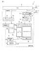
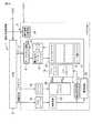
この発明の第1の実施形態に係る半導体装置について説明する。図1は、本実施形態に係るシステムLSIのブロック図である。[First Embodiment]
A semiconductor device according to a first embodiment of the present invention will be described. FIG. 1 is a block diagram of a system LSI according to the present embodiment.
図示するようにシステムLSI1は、CPU2及び半導体記憶装置(EEPROM)3を備えている。CPU1とEEPROM2とは、図示せぬデータバスによって互いにデータを授受可能に接続されている。 As shown, the
EEPROM3は、例えばNOR型フラッシュメモリであり、CPU2が動作するために必要なプログラムやデータ等を保持する。CPU2は、EEPROM3に保持されたデータ等を用いて各種の演算処理を行う。CPU2及びEEPROM3には、外部からクロックCLKが入力される。そしてCPU2はクロックCLKに同期して動作し、EEPROM3はクロックCLKに同期してデータを出力する。 The EEPROM 3 is, for example, a NOR type flash memory, and holds programs and data necessary for the
次に、EEPROM3の構成の詳細について説明する。図1に示すようにEEPROM3は、メモリセルアレイ10、ロウデコーダ11、カラムデコーダ12、カラムセレクタ13、ソース線ドライバ14、書き込みデータバッファ15、センスアンプ16、データ入出力回路17、入力バッファ18、アドレスバッファ19、アドレスレジスタ20、電圧発生回路21、電源回路22、及び制御回路23を備えている。 Next, details of the configuration of the
メモリセルアレイ10は、マトリクス状に配置された複数のNOR型フラッシュメモリセルを備えている。各メモリセルは、ビット線、ワード線、及びソース線に接続されている。ロウデコーダ11は、メモリセルアレイ10のロウ方向を選択する。すなわち、ワード線を選択する。カラムデコーダ12は、メモリセルアレイ10のカラム方向を選択する。カラムセレクタ13は、カラムデコーダ12の選択動作に基づいてビット線を選択し、ビット線を書き込みデータバッファ15またはセンスアンプ16に接続する。ソース線ドライバ14はソース線に電圧を与える。センスアンプ16は、ロウデコーダ11及びカラムデコーダ12によって選択されたメモリセルから読み出されたデータをセンスして増幅する。書き込みデータバッファ15は、メモリセルに対して書き込むべきデータを保持し、所定のメモリセル単位で、一括してデータをメモリセルに書き込む。 The
入力バッファ18は、CPU2から与えられる制御信号を受信し、制御回路23へ出力する。制御信号は、例えばチップイネーブル信号、ライトイネーブル信号、アウトプットイネーブル信号などである。チップイネーブル信号は、EEPROM3を動作可能とする信号である。ライトイネーブル信号は、EEPROM3に対してデータを書き込み可能とする信号である。またアウトプットイネーブル信号は、EEPROM3に対してデータを出力可能とする信号である。アドレスバッファ19は、CPU2から与えられるアドレスを受信し、アドレスレジスタ20へ出力する。 The
データ入出力回路17は、CPU2から与えられる書き込みデータを受け取り、書き込みデータバッファ15に転送する。また、センスアンプ16で増幅されたデータを、クロックに同期して連続的にCPU2へ出力する。 The data input /
アドレスレジスタ20は、アドレスバッファ19から与えられるアドレスに従って、カラムデコーダ12に対してカラムアドレスCAを出力し、ロウデコーダ11に対してロウアドレスRAを出力する。カラムデコーダ12及びロウデコーダ11はそれぞれ、カラムアドレスCA及びロウアドレスRAに基づいて、ビット線及びワード線の選択動作を行う。 The address register 20 outputs a column address CA to the
電圧発生回路21は、外部電圧に従って電圧を発生する。電圧発生回路21によって発生された電圧は、例えばロウデコーダ11、メモリセルアレイ10、書き込みデータバッファ15、センスアンプ16等に与えられる。 The
電源回路22は、バンドギャップリファレンス(band gap reference)回路である。以下、電源回路22をバンドギャップリファレンス回路22と呼ぶ。バンドギャップリファレンス回路22は電圧VBGRを発生し、データ入出力回路17に供給する。データ入出力回路17は、電圧発生回路21で発生された電圧では無く、バンドギャップリファレンス回路22で発生された電圧VBGRを電源電圧として用いて動作する。
制御回路36は、上記回路の動作を制御する。The
The
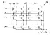
次に図2を用いてメモリセルアレイ10の構成について説明する。図2はメモリセルアレイの構成を示す回路図である。図示するように、メモリセルアレイ20は((m+1)×(n+1))個(m、nは自然数)のメモリセルMCを備えている。メモリセルMCは、電荷蓄積層(例えばフローティングゲート)と制御ゲートとを含む積層ゲートを備えたMOSトランジスタである。そして、同一行にあるメモリセルMCの制御ゲートは、同一のワード線WL0〜WLmのいずれかに共通接続される。また同一列にあるメモリセルMCのドレインは、同一のビット線BL0〜BLnのいずれかに共通接続される。更にメモリセルMCのソースは、同一のソース線SLに共通接続される。 Next, the configuration of the
次にメモリセルMCの断面構成について図3を用いて説明する。図3はメモリセルアレイ10の一部領域の断面図である。図示するように、p型半導体基板30の表面領域内にn型ウェル領域31が形成され、n型ウェル領域31の表面領域内にはp型ウェル領域32が形成されている。p型ウェル領域32上にはゲート絶縁膜33が形成され、ゲート絶縁膜33上に、メモリセルMCのゲート電極が形成されている。メモリセルMCのゲート電極は、ゲート絶縁膜33上に形成された多結晶シリコン層34、多結晶シリコン層34上にゲート間絶縁膜35を介在して形成された多結晶シリコン層36を有している。ゲート間絶縁膜35は、例えばシリコン酸化膜、またはシリコン酸化膜とシリコン窒化膜との積層構造であるON膜、NO膜、またはONO膜で形成される。多結晶シリコン層34はフローティングゲート(FG)として機能し、メモリセルMC毎に分離されている。他方、多結晶シリコン層36はビット線に直交する方向で隣接するもの同士で共通接続されており、コントロールゲート(ワード線WL)として機能する。隣接するゲート電極間に位置するp型ウェル領域32表面内には、n+型不純物拡散層37が形成されている。不純物拡散層37は隣接するトランジスタ同士で共用されており、ソース領域またはドレイン領域として機能する。そして、メモリセルMCのソース領域はソース線SLに接続され、ドレインはビット線BLに接続される。更にp型ウェル領域32の表面領域内にはp+型不純物拡散層38が形成され、n型ウェル領域31の表面領域内にはn+型不純物拡散層39が形成されている。p型ウェル領域32に対しては、不純物拡散層38を介してソース線SLと同じ電位が与えられ、n型ウェル領域31に対しては、不純物拡散層39を介してウェル電圧VNWが与えられる。Next, a cross-sectional configuration of the memory cell MC will be described with reference to FIG. FIG. 3 is a cross-sectional view of a partial region of the
次に、バンドギャップリファレンス回路22の構成について図4を用いて説明する。図4はバンドギャップリファレンス回路22の回路図である。図示するようにバンドギャップリファレンス回路22は、オペアンプ40、抵抗素子41〜43、pチャネルMOSトランジスタ44、ダイオード45、及びN個のダイオード46を備えている。ダイオード46の数は、例えば100個である(N=100)。 Next, the configuration of the band
MOSトランジスタ44は、ゲートがオペアンプ40の出力端子に接続され、ソースに電源電圧VDDが与えられている。抵抗素子41は、一端がMOSトランジスタ44のドレインに接続され、他端がダイオード45のアノードに接続されている。ダイオード45のカソードは接地されている。抵抗素子42は、一端がMOSトランジスタ44のドレインに接続され、他端が抵抗素子43の一端に接続されている。抵抗素子43の他端は、N個のダイオード46のアノードに接続されている。ダイオード46のカソードは接地されている。抵抗素子41の他端とダイオード45のアノードとの接続ノードは、オペアンプ40の反転入力端子(−)に接続されている。また抵抗素子42の他端と抵抗素子43の一端との接続ノードは、オペアンプ40の正入力端子(+)に接続されている。そして、MOSトランジスタ44のドレインと抵抗素子41、42の一端との接続ノードにおける電圧が、バンドギャップリファレンス回路22の出力電圧VBGRとして出力される。The
バンドギャップリファレンス回路22の出力電圧VBGRは、抵抗素子41〜43の抵抗値をそれぞれR1〜R3、ダイオード45における電圧降下をVf1とすると、下記の(1)式で表される。
VBGR=Vf1+(R2/R3)・VT・ln(N・R2/R1)…(1)
但しVTは温度電圧であり、VT=kT/qである。kはボルツマン定数、Tは絶対温度、qは電子の電荷量である。電圧VBGRの温度特性は、上記(1)式を温度で微分した下記の(2)式で表される。
dVBGR/dT=dVf1/dT+(R2/R3)・(k/q)・ln(N・R2/R1)…(2)
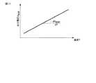
上記(2)式において、第1項はバンドギャップリファレンス回路22に含まれる半導体素子の特性で決まる変数であり、第2項は抵抗素子41〜43の抵抗比で決まる変数である。バンドギャップリファレンス回路22では、第1項による電圧VBGR温度変化を、第2項によって相殺するように、第2項の抵抗比が設定されている。従って、電圧VBGRは温度によらず一定の値となる。図5は、バンドギャップリファレンス回路22の温度特性を示すグラフであり、横軸に温度T、縦軸に出力電圧VBGRを示したものである。図示するように、電圧VBGRは、温度Tに対して一定となっている。The output voltage VBGR of the
VBGR = Vf1 + (R2 / R3) · VT · ln (N · R2 / R1) (1)
However, VT is a temperature voltage and VT = kT / q. k is the Boltzmann constant, T is the absolute temperature, and q is the charge amount of electrons. The temperature characteristic of the voltage VBGR is expressed by the following equation (2) obtained by differentiating the above equation (1) with respect to temperature.
dVBGR / dT = dVf1 / dT + (R2 / R3) · (k / q) · ln (N · R2 / R1) (2)
In the above equation (2), the first term is a variable determined by the characteristics of the semiconductor elements included in the band
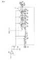
次に、データ入出力回路17の構成について図6を用いて説明する。図6はデータ入出力回路17の回路図である。図示するようにデータ入出力回路17は、NANDゲート50、インバータ51、複数のフリップフロップ52、複数の出力前段回路53、及び複数の出力バッファ回路54を備えている。 Next, the configuration of the data input /
NANDゲート50は、外部からEEPROM3のクロック入力パッド55に入力されるクロックCLKと、イネーブル信号とのNAND演算を行う。イネーブル信号は、EEPROM3がスタンバイ状態であるか否かを示す信号である。イネーブル信号が“H”レベルの場合には、EEPROM3はスタンバイ状態となり、動作を行わない。逆に“L”レベルの場合にはスタンバイ状態から解放されて動作可能状態となる。インバータ51は、NANDゲート50におけるNAND演算結果を反転させ、反転結果を内部クロックICLKとして出力する。すなわち、NANDゲート50及びインバータ51は内部クロックICLK生成回路として機能する。 The
フリップフロップ52は、インバータ51から与えられる内部クロックICLKに応答して動作する。そしてフリップフロップ52は、センスアンプ16から読み出された読み出しデータを内部クロックICLKに同期して格納し、次の内部クロックICLKに同期して当該データを出力する。フリップフロップ52は、例えば複数のトランジスタ群によって構成される。 Flip-
出力前段回路53は、フリップフロップ52から与えられるデータに応じて、出力バッファ回路54を制御する。出力バッファ回路54は、出力前段回路53の制御に基づいてデータを出力する。出力バッファ回路54から出力されるデータは、EEPROM3のデータ出力パッドからCPU2へ出力される。 The
上記構成のデータ入出力回路17は、バンドギャップリファレンス回路22が出力する電圧VBGRを電源電圧として用いて動作する。すなわち、NANDゲート50及びインバータ51を含む内部クロックICLK生成回路、フリップフロップ52、出力前段回路53、及び出力バッファ回路54の電源電圧は、温度に対して依存しない一定電圧VBGRが電源電圧として供給される。The data input /
出力前段回路53及び出力バッファ回路54の構成について図7を用いて説明する。図7は出力前段回路53及び出力バッファ回路54の回路図である。まず出力前段回路53の構成について説明する。 The configurations of the
図示するように出力前段回路53は、pMOSドライバ回路60及びnMOSドライバ回路61を備えている。pMOSドライバ回路60は、pチャネルMOSトランジスタ62、nチャネルMOSトランジスタ63、及び抵抗素子64を備えている。MOSトランジスタ62のソースには電圧VBGRが印加され、ソースは抵抗素子64の一端に接続され、ゲートにはフリップフロップ52から与えられるデータが入力される。MOSトランジスタ63のソースは接地され、ドレインは抵抗素子64の他端に接続され、ゲートにはフリップフロップ52から与えられるデータが入力される。そして、MOSトランジスタ62のドレインと抵抗素子64の一端との接続ノードが、pMOSドライバ回路60の出力ノードとなる。As shown in the figure, the
nMOSドライバ回路61は、pチャネルMOSトランジスタ65、nチャネルMOSトランジスタ66、及び抵抗素子67を備えている。MOSトランジスタ65のソースには電圧VBGRが印加され、ソースは抵抗素子67の一端に接続され、ゲートにはフリップフロップ52から与えられるデータが入力される。MOSトランジスタ66のソースは接地され、ドレインは抵抗素子67の他端に接続され、ゲートにはフリップフロップ52から与えられるデータが入力される。そして、MOSトランジスタ66のドレインと抵抗素子67の他端との接続ノードが、nMOSドライバ回路61の出力ノードとなる。The nMOS driver circuit 61 includes a p-
次に出力バッファ回路54について説明する。図示するように出力バッファ回路54は、pチャネルMOSトランジスタ68及びnチャネルMOSトランジスタ69を備えている。MOSトランジスタ68のソースには電圧VBGRが印加され、ソースはMOSトランジスタ69のドレインに接続され、ゲートはpMOSドライバ回路60の出力ノードに接続される。MOSトランジスタ69のソースは接地され、ゲートはnMOSドライバ回路61の出力ノードに接続される。そして、MOSトランジスタ68のドレインとMOSトランジスタ69のドレインとの接続ノードが、出力バッファ回路54の出力ノードとなり、出力パッドに接続される。Next, the
出力前段回路53は出力バッファ回路54のドライブ回路として機能する。すなわち、出力バッファ回路54に含まれるMOSトランジスタ68、69は、それぞれ出力前段回路53に含まれるpMOSドライバ回路60及びnMOSドライバ回路61によってドライブされる。なお、抵抗素子64、67は、MOSトランジスタ68、69が同時にオン状態とされないよう、各トランジスタのドライブタイミングをずらすために設けられている。 The
上記構成のEEPROM3は、前述の通りバーストアクセスを行う。この様子を図8に示す。図8は、データの読み出し時におけるクロックCLKと、EEPROM3からの出力データ(読み出しデータ)のタイミングチャートである。図示するようにデータは、クロックに同期して連続的に出力される。EEPROM3に対して、読み出すべきデータの先頭アドレスが入力されると、EEPROM3の例えばアドレスバッファ19がアドレスをインクリメントすることにより、先頭アドレスから順に連続したアドレスを発生する。そして発生されたアドレスに応じたメモリセルMCからデータが読み出される。読み出されたデータは、センスアンプ16で増幅されてデータ入出力回路17に入力される。データ入出力回路17においては、フリップフロップ52がデータを内部クロックに同期して取り込み、且つ内部クロックに同期して出力前段回路53へ出力する。従って出力バッファ回路54は、内部クロックに同期して出力前段回路53によりドライブされる。その結果、出力バッファ回路54からデータが内部クロックに同期して外部へ出力される。 The
例えば、センスアンプ16から“1”データが、あるクロックのエッジでフリップフロップ52に入力されたとする。すると、フリップフロップ52は次のクロックのエッジで“1”データを出力前段回路53へ出力する。“1”データが入力されたことにより出力前段回路53では、nチャネルMOSトランジスタ63、66がオン状態となる。従って、pMOSドライバ回路60及びnMOSドライバ回路61の出力は“L”レベルとなる。その結果、出力バッファ回路54ではpチャネルMOSトランジスタ68が駆動されるので、出力バッファ回路54は“H”レベル、すなわち“1”データを出力する。 For example, it is assumed that “1” data is input from the
センスアンプ16が“0”データを出力する場合には、逆に出力バッファ回路におけるnチャネルMOSトランジスタ69が駆動されるので、出力バッファ回路54は“0”データを出力する。 When the
以上のように、この発明の第1の実施形態に係るEEPROMであると、下記(1)の効果が得られる。
(1)データ出力タイミングの設計を簡略化出来る(その1)。
本実施形態に係るEEPROMであると、データを出力するデータ入出力回路17の電源電圧として、EEPROM3の外部から与えられる電圧では無く、バンドギャップリファレンス回路22から与えられる電圧VBGRを用いている。従って、EEPROM3のデータ出力タイミングの設計を簡略化出来る。本効果について以下説明する。As described above, with the EEPROM according to the first embodiment of the present invention, the following effect (1) can be obtained.
(1) The data output timing design can be simplified (part 1).
In the EEPROM according to the present embodiment, the voltage VBGR supplied from the
図9は、クロックと、EEPROM3から出力されCPU2へ与えられるデータのタイミングチャートである。例えばクロックの立ち上がりエッジでCPU2がデータを取り込む場合を考える。すると背景技術で述べたように、データはセットアップのために、クロックの立ち上がりエッジである時刻t1よりも前の時刻t0で、CPU2に出力されていなければならない。このセットアップタイムを以下tsetと呼ぶ。また、ホールドのためにデータは、少なくとも時刻t1から時刻t2までの期間、出力されつづけなければならない。以下ホールドタイムをtholdと呼ぶ。すると、クロックの1周期の長さをtCLKと呼ぶことにすると図9に示すように、クロックの立ち上がりエッジ(時刻t1)からデータが出力されつづけるデータ出力期間toutは、ホールドタイムthold以上、且つ(tCLK−tset)以下でなければならない。換言すれば、データ出力期間toutの終了時刻は、ホールドタイムが終了する時刻t2から、次のデータに関するセットアップタイムの開始時刻t3までの期間になければならない。つまり、データ出力期間toutの終了時刻は、(tCLK−tset−thold)=twindowの間に設定されなければならない。そしてこの期間twindowは、クロックの周波数が高くなるにつれて短くなる。更に、データの出力速度は、外部電圧に依存して変動する。従って、近年、非常に短くなりつつある期間twindowの間に、データ出力期間toutの終了時刻を設定することは困難となっている。 FIG. 9 is a timing chart of a clock and data output from the
この様子を図10に示す。図10は、EEPROM3のデータ出力速度の外部電圧依存性を示しており、横軸に外部電圧、縦軸にデータ出力速度を示している。図中において、外部電圧を用いてデータ入出力回路17を駆動する場合を破線で示し、本実施形態を実線で示す。 This is shown in FIG. FIG. 10 shows the external voltage dependency of the data output speed of the
図示するように、データ入出力回路17を外部電圧で駆動する場合、データ出力速度は外部電圧の上昇と共に速くなる。つまり、外部電圧の変動に伴ってデータ出力速度が変動する。従って、外部電圧のある値でデータ出力期間toutの終了時刻をtwindow内になるように設定したとしても、外部電圧が変動するとtwindowからはずれるおそれがある。 As shown in the figure, when the data input /
しかし本実施形態に係る構成であると、データ入出力回路17を外部電圧でなく、バンドギャップリファレンス回路22で生成した電圧VBGRで駆動している。そして電圧VBGRの値は温度によらず一定である。従って、図10に示すようにEEPROM3のデータの出力速度、すなわちデータ入出力回路17のデータ出力速度は、外部電圧によらず一定である。よって、データ出力期間toutが外部電圧によって変動することを防止出来る。その結果、データ出力タイミングの設計を簡略化出来る。However, in the configuration according to the present embodiment, the data input /
[第2の実施形態]
次に、この発明の第2の実施形態に係る半導体装置について説明する。本実施形態は、上記第1の実施形態において、バンドギャップリファレンス回路22の出力する電圧VBGRに温度特性を持たせたものである。バンドギャップリファレンス回路22の温度特性以外は第1の実施形態と同様であるので、温度特性以外の説明は省略する。[Second Embodiment]
Next explained is a semiconductor device according to the second embodiment of the invention. In this embodiment, the voltage VBGR output from the
図11は、本実施形態に係るEEPROM3の備えるバンドギャップリファレンス回路22の温度特性を示すグラフであり、横軸に温度、縦軸に電圧VBGRを示している。図示するように、温度Tの上昇と共に、電圧VBGRも上昇する。この上昇の度合いが、第1の実施形態で説明した(2)式のdVBGR/dTである。dVBGR/dTは、次のようにして決定される。FIG. 11 is a graph showing the temperature characteristics of the
半導体素子は、外部電圧だけでなく温度によってもその特性が変化する。例えばデータ入出力回路17に着目すると、温度が上昇するとデータ出力速度が低下し、温度が低下すると向上するのが一般的である。また、第1の実施形態で説明したように、電源電圧が上昇するとデータ出力速度は向上し、低下すると遅くなる。従ってdVBGR/dTは正の値を有し、データ出力速度の温度依存性を相殺するように設定される。dVBGR/dTの設定方法は、上記(2)式における抵抗比(R2/R3)、(R2/R1)を変えることで設定出来る。The characteristics of semiconductor elements change not only with external voltage but also with temperature. For example, focusing on the data input /
上記のように、この発明の第2の実施形態に係るEEPROMであると、第1の実施形態で説明した(1)の効果に加えて、下記(2)の効果が得られる。
(2)データ出力タイミングの設計を簡略化出来る(その2)。
本実施形態に係る構成であると、バンドギャップリファレンス回路22の出力する電圧VBGRに、データ入出力回路17におけるデータ出力速度の温度特性と逆の温度特性を持たせている。従って、データ出力タイミングの設計を簡略化出来る。この点につき、図12を用いて説明する。図12は、EEPROM3のデータ出力速度の外部電圧依存性を示しており、横軸に外部電圧、縦軸にデータ出力速度を示している。図中において、dVBGR/dT=0の場合を破線で示し、本実施形態を実線で示す。As described above, the EEPROM according to the second embodiment of the present invention has the following effect (2) in addition to the effect (1) described in the first embodiment.
(2) Data output timing design can be simplified (part 2).
In the configuration according to the present embodiment, the voltage VBGR output from the
図示するように、dVBGR/dT=0、すなわちVBGRが温度に対して一定であると、データ出力速度の外部電圧依存性を抑制することは出来るが、温度依存性は残る。従って、温度Tが上昇するにつれてデータ出力速度は低下する。As shown in the figure, when dVBGR / dT = 0, that is, when VBGR is constant with respect to temperature, the external voltage dependency of the data output speed can be suppressed, but the temperature dependency remains. Therefore, the data output speed decreases as the temperature T increases.
しかし本実施形態に係る構成であると、破線で示される温度特性を相殺するように、dVBGR/dTを設定している。この設定方法は、個々の半導体素子の温度特性を測定し、これを相殺するように設定しても良いし、EEPROM全体、またはデータ入出力回路17全体としての温度特性を測定し、これを相殺するように設定しても良い。その結果、図12に示すようにデータ出力速度の温度依存性を抑制出来る。よって、データ出力速度の外部電圧依存性及び温度依存性を抑制し、データ出力タイミングの設計を簡略化出来る。However, in the configuration according to the present embodiment, dVBGR / dT is set so as to cancel out the temperature characteristic indicated by the broken line. In this setting method, the temperature characteristics of individual semiconductor elements may be measured and set so as to cancel them, or the temperature characteristics of the entire EEPROM or the data input /
[第3の実施形態]
次に、この発明の第3の実施形態に係る半導体装置について説明する。本実施形態は、動作周波数に応じて、データ出力タイミングを決定する内部クロックを遅延させる構成に関する。図13は、本実施形態に係るシステムLSI1のブロック図である。[Third Embodiment]
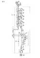
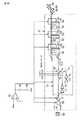
Next explained is a semiconductor device according to the third embodiment of the invention. The present embodiment relates to a configuration for delaying an internal clock that determines data output timing according to an operating frequency. FIG. 13 is a block diagram of the
図示するように本実施形態に係るLSI1は、上記第1の実施形態において電源回路22を廃し、新たに動作速度制御回路24を設け、更にデータ入出力回路17に遅延回路を追加したものである。本実施形態においてデータ入出力回路17は、例えば電圧発生回路21で発生された電圧を電源電圧として用いて動作する。その他の構成は第1の実施形態と同様であるので、説明は省略する。 As shown in the figure, the
データ入出力回路17の構成について図14を用いて説明する。図14はデータ入出力回路17の回路図である。図示するようにデータ入出力回路17は、上記第1の実施形態で説明した図6の構成において、更に遅延回路70を備えている。遅延回路70は、インバータ71〜74、及びスイッチ素子75〜77を備えている。 The configuration of the data input /
インバータ71、72は直列接続され、インバータ71の入力端はインバータ51の出力端に接続されている。インバータ73、74は直列接続され、インバータ73の入力端はインバータ72の出力端に接続されている。スイッチ素子75は、インバータ51の出力を内部クロックICLKとしてフリップフロップ52に与える。スイッチ素子76は、インバータ72の出力を内部クロックICLKとしてフリップフロップ52に与える。スイッチ素子77は、インバータ74の出力を内部クロックICLKとしてフリップフロップ52に与える。スイッチ素子75〜77は、動作速度制御回路24によって与えられる制御信号CNT1〜CNT3によってそれぞれ制御され、いずれか1つのみがオン状態とされる。 The
上記構成において、インバータ71、72、及びインバータ73、74が、インバータ51の出力を遅延させる。従って、スイッチ素子75がオン状態の場合には、インバータ51の出力が内部クロックICLKとなる。すなわち、内部クロックICLKは外部から与えられるクロックCLKに対して殆ど遅延の無い信号である。スイッチ素子76がオン状態の場合には、インバータ51の出力がインバータ71、72で遅延された結果が内部クロックICLKとなる。すなわち、内部クロックICLKはクロックCLKがインバータ71、72で遅延された信号である。スイッチ素子77がオン状態の場合には、インバータ51の出力がインバータ71〜74で遅延された結果が内部クロックICLKとなる。すなわち、内部クロックICLKはクロックCLKがインバータ71〜74で遅延された信号である。従って遅延回路70は、NANDゲート50及びインバータ51と共に内部クロックICLK生成回路として機能する。 In the above configuration, the
スイッチ素子75〜77の具体例について図15を用いて説明する。図15はスイッチ素子75の回路図である。図示するようにスイッチ素子75は、ソース同士、及びドレイン同士が接続されたpチャネルMOSトランジスタ78とnチャネルMOSトランジスタ79を備えている。そして、ソースとドレインのいずれか一方がスイッチ素子75の入力端INとなり、いずれか他方が出力端OUTとなる。そして、MOSトランジスタ79のゲートには制御信号CNT1が入力され、MOSトランジスタ78のゲートには制御信号CNT1の反転信号/CNT1が入力される。スイッチ素子76、77も、制御信号CNT1をCNT2、CNT3に変更する以外は同様の構成を有している。 Specific examples of the
次に、動作速度制御回路24の構成について図16を用いて説明する。図16は動作速度制御回路24の回路図である。図示するように動作速度制御回路24は、カウンタ回路80、比較器81、出力制御回路82、及びデコーダ回路83を備えている。 Next, the configuration of the operation
カウンタ回路80は、制御回路23の命令に応答して、データの読み出し動作の開始と同時にクロックCLKの計数を開始する。比較器81は、動作周波数情報として与えられる待ちクロック数と、カウンタ回路80におけるカウント数とを比較する。待ちクロック数については後述する。出力制御回路82は、比較器81の比較結果に応じて、カウンタ回路80のカウント数が待ちクロック数に達した際に、出力許可信号WAITをデータ入出力回路17に出力する。出力許可信号WAITは、データを外部へ出力することをデータ入出力回路17に許可する信号である。デコーダ回路83は、待ちクロック数をデコードしてクロックCLKの周波数を把握し、制御信号CNT1〜CNT3のいずれかを出力する(アサートする)。 In response to the command from the
図17は、デコーダ回路83における制御信号の出力条件の一例を示す表である。図示するように、待ちクロック数が9以上の場合には、デコーダ回路83は制御信号CNT1をアサートする。つまりスイッチ素子75がオン状態とされる。待ちクロック数が5〜8の場合には制御信号CNT2がアサートされる。つまりスイッチ素子76がオン状態とされる。待ちクロック数が4以下の場合には制御信号CNT3がアサートされる。つまりスイッチ素子77がオン状態とされる。なお図17は一例に過ぎず、待ちクロック数は図17の場合に限られるものでは無いし、図17では待ちクロック数の場合分けが3種類であるが、例えば2種類や4種類以上であっても良い。 FIG. 17 is a table showing an example of output conditions of the control signal in the
次に、上記の待ちクロック数について図18を用いて説明する。図18は、クロックCLKと出力許可信号WAITのタイミングチャートであり、クロックの周波数が3f(f:任意の周波数)の場合(CASE I)、2fの場合(CASE II)、fの場合(CASE III)について示している。 Next, the number of waiting clocks will be described with reference to FIG. FIG. 18 is a timing chart of the clock CLK and the output permission signal WAIT. When the clock frequency is 3f (f: arbitrary frequency) (CASE I), 2f (CASE II), and f (CASE III). ).
バーストアクセスを行うEEPROMではデータを連続して出力するために、最初の読み出し時にはある一定期間、読み出しデータをためておく必要がある。そのために、先頭アドレスに相当するメモリセルMCからデータを読み出してから、一定期間経過後にデータを出力するように、出力許可信号WAITが用いられる。一定期間経過後に出力許可信号WAITがアサートされることで、データ入出力回路17はデータの外部への出力を開始する。この一定期間を、図18では時刻t0からt1までの出力禁止期間Δtとして示している。 In an EEPROM performing burst access, in order to output data continuously, it is necessary to store read data for a certain period at the time of the first read. For this purpose, the output permission signal WAIT is used so that data is output after a certain period of time has elapsed since data was read from the memory cell MC corresponding to the head address. When the output permission signal WAIT is asserted after a certain period of time, the data input /
待ちクロック数とは、上記出力禁止期間Δtに相当するクロック数を意味する。図示するように動作周波数が3fであるCASE Iの場合、出力禁止期間Δtに相当するクロック数(待ちクロック数)が9個であったとする。すると、動作周波数が2fであるCASE IIでは待ちクロック数は6、動作周波数がfであるCASE IIIでは待ちクロック数は3である。つまり、待ちクロック数とはクロックの周波数を示す信号であり、Δtと待ちクロック数との関係から、EEPROM3は動作周波数を把握することが出来る。そして待ちクロック数は、LSI1のユーザによって入力される。 The number of waiting clocks means the number of clocks corresponding to the output inhibition period Δt. As shown in the figure, in the case of CASE I having an operating frequency of 3f, it is assumed that the number of clocks (the number of waiting clocks) corresponding to the output inhibition period Δt is nine. Then, in CASE II where the operating frequency is 2f, the number of waiting clocks is 6, and in CASE III where the operating frequency is f, the number of waiting clocks is 3. That is, the number of waiting clocks is a signal indicating the frequency of the clock, and the
次に、上記構成のEEPROM3におけるデータの出力タイミングについて図19を用いて説明する。図19は、内部クロックICLKと出力データのタイミングチャートであり、CASE I〜IIIについて示している。なお説明の簡単化の為に、以下ではCASE Iの内部クロックは、外部から与えられるクロックCLKに対して全く遅延が無い場合を仮定する。 Next, the data output timing in the
まずCASE Iについて説明する。内部クロックICLKは時刻t0で立ち上がり、それに応答してデータ1が時刻t3で出力される。また内部クロックICLKは時刻t6で立ち上がり、それに応答してデータ2が時刻t9で出力される。 First, CASE I will be described. The internal clock ICLK rises at time t0, and in response,
次にCASE IIについて説明する。内部クロックICLKは時刻t0からΔt1だけ遅れた時刻t1で立ち上がり、それに応答してデータ1が時刻t3からΔt1だけ遅れた時刻t4で出力される。また内部クロックICLKは時刻t6からΔt1だけ遅れた時刻t7で立ち上がり、それに応答してデータ2が時刻t9からΔt1だけ遅れた時刻t10で出力される。遅延時間Δt1は、遅延回路71、72における遅延時間に相当する。 Next, CASE II will be described. The internal clock ICLK rises at time t1 delayed by Δt1 from time t0, and in response,
次にCASE IIIについて説明する。内部クロックICLKは時刻t0からΔt2だけ遅れた時刻t2で立ち上がり、それに応答してデータ1が時刻t3からΔt2だけ遅れた時刻t5で出力される。また内部クロックICLKは時刻t6からΔt2だけ遅れた時刻t8で立ち上がり、それに応答してデータ2が時刻t9からΔt2だけ遅れた時刻t11で出力される。遅延時間Δt2は、遅延回路71〜74における遅延時間に相当する。 Next, CASE III will be described. The internal clock ICLK rises at time t2 delayed by Δt2 from time t0, and in response,
上記のように、この発明の第3の実施形態に係るEEPROMであると、下記(3)の効果が得られる。
(3)データ出力タイミングの設計を簡略化出来る(その3)。
本実施形態に係る構成であると、データ入出力回路17は待ちクロック数に応じてデータの出力タイミングを変化させる。より具体的には、クロックCLKの周波数が低下するにつれて、データの出力タイミングを遅らせる。従って、データ出力タイミングの設計を簡略化出来る。この点につき、図20を用いて説明する。図20は、クロックCLKとデータのタイミングチャートであり、上記CASE I〜IIIについてそれぞれ示している。図20におけるデータの出力タイミングは、図19と同じである。As described above, the EEPROM according to the third embodiment of the present invention has the following effect (3).
(3) The data output timing design can be simplified (part 3).
In the configuration according to the present embodiment, the data input /
一般的に、バーストアクセスを行う半導体メモリにおいては、動作周波数が高いほどホールドタイムとして要求される期間tholdは短く、低いほど長い。つまり、動作周波数によってホールドタイムが変化する。従って、例えば高周波数で動作するCPUに求められるホールドタイムを満たすようにEEPROMを設計した場合、低周波数で動作するCPUに求められるホールドタイムを満たせない場合がある。 In general, in a semiconductor memory that performs burst access, the period thold required as the hold time is shorter as the operating frequency is higher, and is longer as it is lower. That is, the hold time varies depending on the operating frequency. Therefore, for example, when an EEPROM is designed to satisfy a hold time required for a CPU operating at a high frequency, the hold time required for a CPU operating at a low frequency may not be satisfied.
しかし本実施形態に係る構成であると、動作周波数に応じてデータ出力期間を可変にしている。図20に示すように、CASE I〜IIIにおけるデータ出力期間をtout1〜tout3と呼ぶことにする。すると、CASE Iよりも動作周波数の低いCASE IIのデータ出力期間tout2は、tout1よりもΔt1だけ長い。またCASE IIよりも動作周波数の低いCASE IIIのデータ出力期間tout3は、tout1よりもΔt2(>Δt1)だけ長い。すなわち、動作周波数(クロックCLKの周波数)が低下するにつれて、データ出力期間が長くなる。これは、動作周波数(待ちクロック数)に応じて、遅延回路70における遅延時間を変化させているからである。つまり、長いホールドタイムが要求される場合にはデータ出力期間が長くされ、ホールドタイムが短くて良い場合にはデータ出力期間が短くされる。従って、動作周波数が変動した場合でも、データ出力期間を最適にすることが出来、データ出力タイミングの設計を簡略化出来る。そして、EEPROM3を様々な動作周波数に適合させることが出来、EEPROM3の汎用性を向上出来る。 However, in the configuration according to the present embodiment, the data output period is made variable according to the operating frequency. As shown in FIG. 20, the data output periods in CASE I to III are called tout1 to tout3. Then, the data output period tout2 of CASE II having an operating frequency lower than that of CASE I is longer than tout1 by Δt1. In addition, the data output period tout3 of CASE III having an operating frequency lower than that of CASE II is longer than tout1 by Δt2 (> Δt1). That is, as the operating frequency (frequency of clock CLK) decreases, the data output period becomes longer. This is because the delay time in the
[第4の実施形態]
次に、この発明の第4の実施形態に係る半導体装置について説明する。本実施形態は、上記第1の実施形態と第2の実施形態とを組み合わせたものである。図21は、本実施形態に係るシステムLSIのブロック図である。[Fourth Embodiment]
Next explained is a semiconductor device according to the fourth embodiment of the invention. The present embodiment is a combination of the first embodiment and the second embodiment. FIG. 21 is a block diagram of a system LSI according to the present embodiment.
図示するように本実施形態に係るLSI1は、上記第1の実施形態で説明した図1の構成において、上記第3の実施形態で説明した動作速度制御回路24をEEPROM3に設けたものである。その他の構成は第1、第3の実施形態で説明したとおりである。 As shown in the figure, the
図22は、本実施形態に係るデータ入出力回路17の回路図である。図示するように、上記第3の実施形態で説明した図14の構成において、NANDゲート50、インバータ51、及び遅延回路70を含む内部クロックICLK生成回路、フリップフロップ52、出力前段回路53、並びに出力バッファ回路54が、電源回路(バンドギャップリファレンス回路)22の出力電圧VBGRを電源電圧として用いて動作する。FIG. 22 is a circuit diagram of the data input /
本実施形態に係る構成であると、上記第1の実施形態で説明した(1)の効果と、上記第3の実施形態で説明した(3)の効果を併せて得ることが出来る。 With the configuration according to the present embodiment, the effect (1) described in the first embodiment and the effect (3) described in the third embodiment can be obtained together.
なお図22において、電圧VBGRを更に遅延回路70の電源電圧として用いても良い。また、第1の実施形態と第2の実施形態とを組み合わせても良い。すなわち、第4の実施形態に係る構成において、電圧VBGRに温度依存性を持たせても良い。この場合には、上記(1)、(3)の効果に加えて、第2の実施形態で説明した(2)の効果も併せて得られる。In FIG. 22, the voltage VBGR may be further used as a power supply voltage for the
上記のように、この発明の第1、第2、第4の実施形態に係る半導体装置であると、クロックに同期してデータを連続的に出力するデータ入出力回路の電源電圧を、バンドギャップリファレンス回路により発生している。従って、データ入出力回路のデータ出力速度が外部電圧によらず一定となる。その結果、データの出力タイミングの設定を容易にすることが出来る。更に上記第2の実施形態であると、バンドギャップリファレンス回路の出力電圧に、半導体素子の動作特性に関する温度依存性を相殺するように、温度依存性を持たせている。その結果、データ入出力回路のデータ出力速度を、温度に対して一定にすることが出来る。 As described above, in the semiconductor device according to the first, second, and fourth embodiments of the present invention, the power supply voltage of the data input / output circuit that continuously outputs data in synchronization with the clock is It is generated by the reference circuit. Therefore, the data output speed of the data input / output circuit is constant regardless of the external voltage. As a result, the data output timing can be easily set. Further, in the second embodiment, the output voltage of the bandgap reference circuit has temperature dependency so as to cancel out the temperature dependency related to the operating characteristics of the semiconductor element. As a result, the data output speed of the data input / output circuit can be made constant with respect to the temperature.
更に上記第3、第4の実施形態であると、動作周波数に応じてデータ出力期間を可変としている。従って、動作周波数が変動した場合であっても、ホールドタイムを満たすようにデータ出力期間を設定することが出来、半導体装置の汎用性を向上出来る。 Furthermore, in the third and fourth embodiments, the data output period is variable according to the operating frequency. Therefore, even when the operating frequency fluctuates, the data output period can be set so as to satisfy the hold time, and the versatility of the semiconductor device can be improved.
なお第2の実施形態においては、半導体素子の温度特性を相殺するように、電圧VBGRに温度依存性を持たせる場合を例に説明した。しかし、必ずしも半導体素子の温度特性を完全に相殺しなければならないわけでは無い。つまり電圧VBGRは、半導体素子の温度依存性を完全には相殺出来なくても、逆の温度依存性さえあれば、出力速度の温度依存性を抑制することが出来、データ出力タイミングを容易に出来るという効果は得られる。また、出力速度は温度が上昇することで低下する場合を例に説明したが、逆の場合でも適用可能である。すなわち、温度が上昇することで出力速度が上昇するような構成があった場合には、dVBGR/dTが負の値となるように設定すれば良い。更に、データ出力速度と温度との関係が、一次関数的でなく二次関数的であっても、上記実施形態は適用可能である。つまり、全体としての特性が温度に比例するか反比例するかに応じて、dVBGR/dTを決定すればよい。勿論、バンドギャップリファレンス回路22の構成を変形することにより、VBGRの温度特性が二次関数となるようにしても良い。In the second embodiment, the case where the voltage VBGR is given temperature dependency so as to cancel out the temperature characteristics of the semiconductor element has been described as an example. However, it is not always necessary to completely cancel out the temperature characteristics of the semiconductor element. In other words, even if the voltage VBGR cannot completely cancel out the temperature dependency of the semiconductor element, the temperature dependency of the output speed can be suppressed as long as the reverse temperature dependency exists. The effect that you can do it. In addition, the output speed has been described as an example in which the output speed decreases as the temperature increases, but the output speed can also be applied to the reverse case. In other words, when there is a configuration in which the output speed increases as the temperature rises, dVBGR / dT may be set to a negative value. Further, the above embodiment can be applied even if the relationship between the data output speed and the temperature is not a linear function but a quadratic function. That is, dVBGR / dT may be determined according to whether the overall characteristics are proportional to temperature or inversely proportional to temperature. Of course, the temperature characteristics of VBGR may be a quadratic function bymodifying the configuration of the band
また、上記実施形態ではEEPROM3としてNOR型フラッシュメモリの場合を例に説明した。しかしNOR型に限らず、例えばNAND型フラッシュメモリであっても良い。図23はNAND型フラッシュメモリの備えるメモリセルアレイの回路図である。 In the above embodiment, the case where the
図示するようにメモリセルアレイは、複数のNANDセルを有している。図23では1行のNANDセルのみを示しているが複数あっても良い。NANDセルの各々は、32個のメモリセルトランジスタMT0〜MT31と、選択トランジスタST1、ST2とを含んでいる。以下では、説明の簡潔化のために、メモリセルトランジスタMT0〜MT31を単にメモリセルトランジスタMTと呼ぶ。メモリセルトランジスタMTは、半導体基板上にゲート絶縁膜を介在して形成されたフローティングゲートと、フローティングゲート上にゲート間絶縁膜を介在して形成されたコントロールゲートとを有する積層ゲート構造を備えている。なお、メモリセルトランジスタMTの個数は32個に限られず、8個や16個であってもよく、その数は限定されるものではない。メモリセルトランジスタMTは、隣接するもの同士でソース、ドレインを共有している。そして、選択トランジスタST1、ST2間に、その電流経路が直列接続されるようにして配置されている。直列接続されたメモリセルトランジスタMTの一端側のドレイン領域は選択トランジスタST1のソース領域に接続され、他端側のソース領域は選択トランジスタST2のドレイン領域に接続されている。 As shown in the figure, the memory cell array has a plurality of NAND cells. Although only one row of NAND cells is shown in FIG. 23, a plurality of NAND cells may be provided. Each of the NAND cells includes 32 memory cell transistors MT0 to MT31 and select transistors ST1 and ST2. Hereinafter, for simplification of description, the memory cell transistors MT0 to MT31 are simply referred to as memory cell transistors MT. Memory cell transistor MT has a stacked gate structure having a floating gate formed on a semiconductor substrate with a gate insulating film interposed therebetween, and a control gate formed on the floating gate with an inter-gate insulating film interposed therebetween. Yes. The number of memory cell transistors MT is not limited to 32, but may be 8 or 16, and the number is not limited. Adjacent ones of the memory cell transistors MT share a source and a drain. And it arrange | positions so that the current path may be connected in series between selection transistor ST1, ST2. The drain region on one end side of the memory cell transistors MT connected in series is connected to the source region of the select transistor ST1, and the source region on the other end side is connected to the drain region of the select transistor ST2.
同一行にあるメモリセルトランジスタMTのコントロールゲートはワード線WL0〜WL31のいずれかに共通接続され、同一行にあるメモリセルの選択トランジスタST1、ST2のゲートは、それぞれセレクトゲート線SGD、SGSに共通接続されている。また、メモリセルアレイにおいて同一列にある選択トランジスタST1のドレインはビット線BL0〜BLn(nは自然数)のいずれかに共通接続される。選択トランジスタST2のソースはソース線SLに共通接続される。 The control gates of the memory cell transistors MT in the same row are commonly connected to any one of the word lines WL0 to WL31, and the gates of the selection transistors ST1 and ST2 of the memory cells in the same row are common to the select gate lines SGD and SGS, respectively. It is connected. Further, the drains of the select transistors ST1 in the same column in the memory cell array are commonly connected to any one of bit lines BL0 to BLn (n is a natural number). The sources of the selection transistors ST2 are commonly connected to the source line SL.
上記のようなNAND型フラッシュメモリであっても、上記実施形態は適用出来る。またフラッシュメモリに限らず、例えばDRAMやPSRAM(Pseudo SRAM)等、バーストアクセスを行う半導体メモリ全般に適用可能である。 The above embodiment can be applied to the NAND flash memory as described above. Further, the present invention is not limited to the flash memory, and can be applied to all semiconductor memories that perform burst access, such as DRAM and PSRAM (Pseudo SRAM).
また上記実施形態では、電源回路22がバンドギャップリファレンス回路そのものである場合について説明した。しかし電源回路22は、バンドギャップリファレンス回路で発生された電圧VBGRを基準にして別の電圧を発生する構成であっても良い。図24及び図25はこのような場合について示しており、電源回路22の一部及びデータ入出力回路17を示す回路図である。 In the above embodiment, the case where the
図示するように電源回路22は、バンドギャップリファレンス回路の他に比較器90、及び抵抗素子91、92を備えている。図示するように、抵抗素子91の一端は比較器90の出力ノードに接続され、他端は抵抗素子92の一端に接続されている。抵抗素子92の他端は接地されている。比較器の正入力端子には電圧VBGRが入力され、反転入力端子は抵抗素子91の他端と抵抗素子92の一端との接続ノードが接続されている。本構成において、比較器90の出力ノードの電圧が、データ入出力回路17の電源電圧として与えられる。そして比較器90の出力ノードの電圧は、電圧VBGRを基準にして抵抗素子91、92の抵抗比によって決定され、電圧VBGRと等しい温度依存性を有する。As illustrated, the
上記のように、データ入出力回路17の電源電圧として与えられる電圧はVBGRそのものには限られない。そして、VBGRによって制御され且つ温度依存性の抑制された電圧、または電圧VBGRによって制御され且つデータ出力速度の温度依存性とは逆の温度依存性を有する電圧を、データ入出力回路17の電源電圧として用いることが出来る。これは、電圧VBGRは約1.25Vであり、この電圧値がデータ入出力回路17の電源電圧として最適とは限らず、電圧値を変更する必要がある場合があり得るからである。As described above, the voltage applied as the power supply voltage of the data input /
なお、本願発明は上記実施形態に限定されるものではなく、実施段階ではその要旨を逸脱しない範囲で種々に変形することが可能である。更に、上記実施形態には種々の段階の発明が含まれており、開示される複数の構成要件における適宜な組み合わせにより種々の発明が抽出されうる。例えば、実施形態に示される全構成要件からいくつかの構成要件が削除されても、発明が解決しようとする課題の欄で述べた課題が解決でき、発明の効果の欄で述べられている効果が得られる場合には、この構成要件が削除された構成が発明として抽出されうる。 Note that the present invention is not limited to the above-described embodiment, and various modifications can be made without departing from the scope of the invention in the implementation stage. Furthermore, the above embodiments include inventions at various stages, and various inventions can be extracted by appropriately combining a plurality of disclosed constituent elements. For example, even if some constituent requirements are deleted from all the constituent requirements shown in the embodiment, the problem described in the column of the problem to be solved by the invention can be solved, and the effect described in the column of the effect of the invention Can be extracted as an invention.
1…システムLSI、2…CPU、3…EEPROM、10…メモリセルアレイ、11…ロウデコーダ、12…カラムデコーダ、13…カラムセレクタ、14…ソース線ドライバ、15…書き込みデータバッファ、16…センスアンプ、17…データ入出力回路、18…入力バッファ、19…アドレスバッファ、20…アドレスレジスタ、21…電圧発生回路、22…バンドギャップリファレンス回路、23…制御回路、24…動作速度制御回路、40、81、90…比較器、41〜43、64、67、91、92…抵抗素子、44、62、65、68、78…pチャネルMOSトランジスタ、45、46…ダイオード、50…NANDゲート、51、71〜74…インバータ、52…フリップフロップ、53…出力前段回路、54…出力バッファ回路、55…入力パッド、56…出力パッド、60…pMOSドライバ回路、61、63、66、69、79…nMOSドライバ回路、63…nチャネルMOSトランジスタ、70…遅延回路、75〜77…スイッチ素子、80…カウンタ回路、82…出力制御回路、83…デコーダ回路 DESCRIPTION OF
Claims (5)
Translated fromJapanese外部から与えられる前記第1クロックから第2クロックを生成するクロック生成回路と、
前記第2クロックに同期して動作し、前記データが入力されるフリップフロップ回路と、
前記フリップフロップ回路から出力される前記データを外部へ出力する出力バッファ回路と、
バンドギャップリファレンス回路を含み、該バンドギャップリファレンス回路により制御される電圧を発生し、該電圧を前記クロック生成回路、前記フリップフロップ回路及び前記出力バッファ回路へ電源電圧として供給する電源回路と
を具備することを特徴とする半導体装置。A semiconductor device for continuously outputting data in synchronization with a first clock,
A clock generation circuit for generating a second clock from the first clock applied from the outside;
A flip-flop circuit that operates in synchronization with the second clock and receives the data;
An output buffer circuit for outputting the data output from the flip-flop circuit to the outside;
A power supply circuit including a bandgap reference circuit, generating a voltage controlled by the bandgap reference circuit, and supplying the voltage as a power supply voltage to the clock generation circuit, the flip-flop circuit, and the output buffer circuit. A semiconductor device.
前記クロックを遅延させる遅延回路を含むクロック生成回路と、
前記遅延回路で遅延された前記クロックに同期して動作し、前記データが入力されるフリップフロップ回路と、
前記フリップフロップ回路から出力される前記データを外部へ出力する出力バッファ回路と
を具備し、前記遅延回路における遅延時間は、前記クロックの周波数に反比例して変化する
ことを特徴とする半導体装置。A semiconductor device that continuously outputs data in synchronization with a clock,
A clock generation circuit including a delay circuit for delaying the clock;
A flip-flop circuit that operates in synchronization with the clock delayed by the delay circuit and receives the data;
An output buffer circuit that outputs the data output from the flip-flop circuit to the outside, and a delay time in the delay circuit changes in inverse proportion to the frequency of the clock.
前記遅延回路は、前記クロックが入力され、且つ互いに前記遅延時間の異なる複数のクロック遅延部を備え、
前記デコード回路は、前記動作周波数情報に応じていずれかの前記クロック遅延部を動作状態とし、前記クロックの周波数の上昇と共に前記遅延時間の長い前記クロック遅延部を動作状態とする
ことを特徴とする請求項2記載の半導体装置。Decoding operating frequency information input from the outside, further comprising a decoding circuit for grasping the frequency of the clock,
The delay circuit includes a plurality of clock delay units to which the clock is input and whose delay times are different from each other.
The decoding circuit sets one of the clock delay units in an operating state according to the operating frequency information, and sets the clock delay unit having a long delay time in an operating state as the clock frequency increases. The semiconductor device according to claim 2.
ことを特徴とする請求項2記載の半導体装置。A power supply circuit including a bandgap reference circuit, generating a voltage controlled by the bandgap reference circuit, and supplying the voltage as a power supply voltage to the clock generation circuit, the flip-flop circuit, and the output buffer circuit; The semiconductor device according to claim 2.
ことを特徴とする請求項1または4記載の半導体装置。The band gap reference circuit has an output voltage characteristic in which the voltage increases as the temperature rises, and the voltage suppresses temperature dependency and external voltage dependency of the data output speed in the flip-flop circuit and the output buffer circuit. The semiconductor device according to claim 1 or 4, wherein:
Priority Applications (2)
| Application Number | Priority Date | Filing Date | Title |
|---|---|---|---|
| JP2006222640AJP2008048214A (en) | 2006-08-17 | 2006-08-17 | Semiconductor device |
| US11/839,859US7623407B2 (en) | 2006-08-17 | 2007-08-16 | Semiconductor device |
Applications Claiming Priority (1)
| Application Number | Priority Date | Filing Date | Title |
|---|---|---|---|
| JP2006222640AJP2008048214A (en) | 2006-08-17 | 2006-08-17 | Semiconductor device |
Related Child Applications (1)
| Application Number | Title | Priority Date | Filing Date |
|---|---|---|---|
| JP2011232835ADivisionJP2012059354A (en) | 2011-10-24 | 2011-10-24 | Semiconductor device |
Publications (1)
| Publication Number | Publication Date |
|---|---|
| JP2008048214Atrue JP2008048214A (en) | 2008-02-28 |
Family
ID=39181514
Family Applications (1)
| Application Number | Title | Priority Date | Filing Date |
|---|---|---|---|
| JP2006222640AAbandonedJP2008048214A (en) | 2006-08-17 | 2006-08-17 | Semiconductor device |
Country Status (2)
| Country | Link |
|---|---|
| US (1) | US7623407B2 (en) |
| JP (1) | JP2008048214A (en) |
Cited By (2)
| Publication number | Priority date | Publication date | Assignee | Title |
|---|---|---|---|---|
| JP2009016017A (en)* | 2007-07-09 | 2009-01-22 | Samsung Electronics Co Ltd | Semiconductor integrated circuit |
| JP2010165397A (en)* | 2009-01-14 | 2010-07-29 | Toshiba Corp | Nonvolatile semiconductor memory device |
Families Citing this family (1)
| Publication number | Priority date | Publication date | Assignee | Title |
|---|---|---|---|---|
| KR102789857B1 (en)* | 2020-08-31 | 2025-04-03 | 에스케이하이닉스 주식회사 | Storage device and operating method thereof |
Citations (7)
| Publication number | Priority date | Publication date | Assignee | Title |
|---|---|---|---|---|
| JPH0334566A (en)* | 1989-06-26 | 1991-02-14 | American Teleph & Telegr Co <Att> | Cmos-ecl output buffer circuit |
| JPH06326587A (en)* | 1993-05-13 | 1994-11-25 | Nec Corp | Semiconductor integrated circuit device |
| JPH07253824A (en)* | 1994-03-14 | 1995-10-03 | Toshiba Corp | Operation speed automatic correction circuit and communication control circuit |
| JP2000123570A (en)* | 1998-10-13 | 2000-04-28 | Fujitsu Ltd | Semiconductor device |
| JP2001094055A (en)* | 1999-09-24 | 2001-04-06 | Toshiba Corp | Semiconductor device and reference potential adjusting method thereof |
| JP2003133942A (en)* | 2001-10-29 | 2003-05-09 | Mitsubishi Electric Corp | Semiconductor device |
| JP2004350290A (en)* | 2003-05-20 | 2004-12-09 | Toshiba Corp | Bandgap voltage reference generator circuit, heat detection circuit, and integrated circuit |
Family Cites Families (4)
| Publication number | Priority date | Publication date | Assignee | Title |
|---|---|---|---|---|
| JP4221764B2 (en)* | 1997-04-25 | 2009-02-12 | 沖電気工業株式会社 | Semiconductor memory device |
| JP3519361B2 (en) | 2000-11-07 | 2004-04-12 | Necエレクトロニクス株式会社 | Bandgap reference circuit |
| JP4274811B2 (en) | 2003-02-17 | 2009-06-10 | 株式会社ルネサステクノロジ | Synchronous semiconductor memory device |
| JP4282412B2 (en) | 2003-09-02 | 2009-06-24 | 株式会社東芝 | Current source circuit |
- 2006
- 2006-08-17JPJP2006222640Apatent/JP2008048214A/ennot_activeAbandoned
- 2007
- 2007-08-16USUS11/839,859patent/US7623407B2/enactiveActive
Patent Citations (7)
| Publication number | Priority date | Publication date | Assignee | Title |
|---|---|---|---|---|
| JPH0334566A (en)* | 1989-06-26 | 1991-02-14 | American Teleph & Telegr Co <Att> | Cmos-ecl output buffer circuit |
| JPH06326587A (en)* | 1993-05-13 | 1994-11-25 | Nec Corp | Semiconductor integrated circuit device |
| JPH07253824A (en)* | 1994-03-14 | 1995-10-03 | Toshiba Corp | Operation speed automatic correction circuit and communication control circuit |
| JP2000123570A (en)* | 1998-10-13 | 2000-04-28 | Fujitsu Ltd | Semiconductor device |
| JP2001094055A (en)* | 1999-09-24 | 2001-04-06 | Toshiba Corp | Semiconductor device and reference potential adjusting method thereof |
| JP2003133942A (en)* | 2001-10-29 | 2003-05-09 | Mitsubishi Electric Corp | Semiconductor device |
| JP2004350290A (en)* | 2003-05-20 | 2004-12-09 | Toshiba Corp | Bandgap voltage reference generator circuit, heat detection circuit, and integrated circuit |
Cited By (2)
| Publication number | Priority date | Publication date | Assignee | Title |
|---|---|---|---|---|
| JP2009016017A (en)* | 2007-07-09 | 2009-01-22 | Samsung Electronics Co Ltd | Semiconductor integrated circuit |
| JP2010165397A (en)* | 2009-01-14 | 2010-07-29 | Toshiba Corp | Nonvolatile semiconductor memory device |
Also Published As
| Publication number | Publication date |
|---|---|
| US20080089165A1 (en) | 2008-04-17 |
| US7623407B2 (en) | 2009-11-24 |
Similar Documents
| Publication | Publication Date | Title |
|---|---|---|
| US8094512B2 (en) | Semiconductor memory device with individual and selective refresh of data storage banks | |
| US8385128B2 (en) | Semiconductor memory | |
| JP4427382B2 (en) | Nonvolatile semiconductor memory device | |
| US7486565B2 (en) | Semiconductor memory device with memory cells each including a charge accumulation layer and a control gate | |
| JP4709525B2 (en) | Nonvolatile semiconductor memory device | |
| US7590003B2 (en) | Self-reference sense amplifier circuit and sensing method | |
| US7439782B2 (en) | Semiconductor integrated circuit device with power-on reset circuit for detecting the operating state of an analog circuit | |
| US20070268752A1 (en) | Nonvolatile semiconductor memory device | |
| US6940762B2 (en) | Semiconductor memory device including MOS transistor having a floating gate and a control gate | |
| JP2008027493A (en) | Semiconductor memory device | |
| US10706917B2 (en) | Semiconductor memory device | |
| JP2011009496A (en) | Semiconductor device | |
| US8558602B2 (en) | Semiconductor integrated circuit | |
| JP2008048214A (en) | Semiconductor device | |
| KR100699370B1 (en) | A memory card including a semiconductor memory device having a plurality of MOOS transistors each having a floating gate and a control gate, and a semiconductor memory device. | |
| US6643203B2 (en) | Semiconductor memory device including clock-independent sense amplifier | |
| JP2012059354A (en) | Semiconductor device | |
| JP5017443B2 (en) | Memory system | |
| JP3963420B2 (en) | Semiconductor memory device | |
| JP5095083B2 (en) | Nonvolatile semiconductor memory device | |
| JP5025785B2 (en) | Semiconductor memory device | |
| JP5789803B2 (en) | Semiconductor memory and system | |
| Itoh et al. | Memory at VLSI circuits symposium | |
| JP2001028193A (en) | Semiconductor memory | |
| CN118057926A (en) | Semiconductor memory device with a memory cell having a memory cell with a memory cell having a memory cell |
Legal Events
| Date | Code | Title | Description |
|---|---|---|---|
| A621 | Written request for application examination | Free format text:JAPANESE INTERMEDIATE CODE: A621 Effective date:20080922 | |
| A977 | Report on retrieval | Free format text:JAPANESE INTERMEDIATE CODE: A971007 Effective date:20101227 | |
| A131 | Notification of reasons for refusal | Free format text:JAPANESE INTERMEDIATE CODE: A131 Effective date:20110104 | |
| A521 | Request for written amendment filed | Free format text:JAPANESE INTERMEDIATE CODE: A523 Effective date:20110223 | |
| A131 | Notification of reasons for refusal | Free format text:JAPANESE INTERMEDIATE CODE: A131 Effective date:20110823 | |
| A521 | Request for written amendment filed | Free format text:JAPANESE INTERMEDIATE CODE: A523 Effective date:20111024 | |
| A01 | Written decision to grant a patent or to grant a registration (utility model) | Free format text:JAPANESE INTERMEDIATE CODE: A01 Effective date:20120321 | |
| A762 | Written abandonment of application | Free format text:JAPANESE INTERMEDIATE CODE: A762 Effective date:20120419 |