JP2008042088A - Thin film device and manufacturing method thereof - Google Patents
Thin film device and manufacturing method thereofDownload PDFInfo
- Publication number
- JP2008042088A JP2008042088AJP2006217272AJP2006217272AJP2008042088AJP 2008042088 AJP2008042088 AJP 2008042088AJP 2006217272 AJP2006217272 AJP 2006217272AJP 2006217272 AJP2006217272 AJP 2006217272AJP 2008042088 AJP2008042088 AJP 2008042088A
- Authority
- JP
- Japan
- Prior art keywords
- film
- oxide semiconductor
- insulator
- semiconductor film
- thin film
- Prior art date
- Legal status (The legal status is an assumption and is not a legal conclusion. Google has not performed a legal analysis and makes no representation as to the accuracy of the status listed.)
- Granted
Links
Images


Classifications
- H—ELECTRICITY
- H01—ELECTRIC ELEMENTS
- H01L—SEMICONDUCTOR DEVICES NOT COVERED BY CLASS H10
- H01L21/00—Processes or apparatus adapted for the manufacture or treatment of semiconductor or solid state devices or of parts thereof
- H01L21/02—Manufacture or treatment of semiconductor devices or of parts thereof
- H01L21/02104—Forming layers
- H01L21/02365—Forming inorganic semiconducting materials on a substrate
- H01L21/02518—Deposited layers
- H01L21/02521—Materials
- H01L21/02551—Group 12/16 materials
- H01L21/02554—Oxides
- H—ELECTRICITY
- H01—ELECTRIC ELEMENTS
- H01L—SEMICONDUCTOR DEVICES NOT COVERED BY CLASS H10
- H01L21/00—Processes or apparatus adapted for the manufacture or treatment of semiconductor or solid state devices or of parts thereof
- H01L21/02—Manufacture or treatment of semiconductor devices or of parts thereof
- H01L21/02104—Forming layers
- H01L21/02365—Forming inorganic semiconducting materials on a substrate
- H01L21/02518—Deposited layers
- H01L21/02587—Structure
- H—ELECTRICITY
- H01—ELECTRIC ELEMENTS
- H01L—SEMICONDUCTOR DEVICES NOT COVERED BY CLASS H10
- H01L21/00—Processes or apparatus adapted for the manufacture or treatment of semiconductor or solid state devices or of parts thereof
- H01L21/02—Manufacture or treatment of semiconductor devices or of parts thereof
- H01L21/02104—Forming layers
- H01L21/02365—Forming inorganic semiconducting materials on a substrate
- H01L21/02656—Special treatments
- H01L21/02664—Aftertreatments
- H01L21/02694—Controlling the interface between substrate and epitaxial layer, e.g. by ion implantation followed by annealing
- H—ELECTRICITY
- H10—SEMICONDUCTOR DEVICES; ELECTRIC SOLID-STATE DEVICES NOT OTHERWISE PROVIDED FOR
- H10D—INORGANIC ELECTRIC SEMICONDUCTOR DEVICES
- H10D30/00—Field-effect transistors [FET]
- H10D30/60—Insulated-gate field-effect transistors [IGFET]
- H10D30/67—Thin-film transistors [TFT]
- H10D30/6704—Thin-film transistors [TFT] having supplementary regions or layers in the thin films or in the insulated bulk substrates for controlling properties of the device
- H10D30/6713—Thin-film transistors [TFT] having supplementary regions or layers in the thin films or in the insulated bulk substrates for controlling properties of the device characterised by the properties of the source or drain regions, e.g. compositions or sectional shapes
- H—ELECTRICITY
- H10—SEMICONDUCTOR DEVICES; ELECTRIC SOLID-STATE DEVICES NOT OTHERWISE PROVIDED FOR
- H10D—INORGANIC ELECTRIC SEMICONDUCTOR DEVICES
- H10D30/00—Field-effect transistors [FET]
- H10D30/60—Insulated-gate field-effect transistors [IGFET]
- H10D30/67—Thin-film transistors [TFT]
- H10D30/6729—Thin-film transistors [TFT] characterised by the electrodes
- H10D30/6737—Thin-film transistors [TFT] characterised by the electrodes characterised by the electrode materials
- H10D30/6739—Conductor-insulator-semiconductor electrodes
- H—ELECTRICITY
- H10—SEMICONDUCTOR DEVICES; ELECTRIC SOLID-STATE DEVICES NOT OTHERWISE PROVIDED FOR
- H10D—INORGANIC ELECTRIC SEMICONDUCTOR DEVICES
- H10D30/00—Field-effect transistors [FET]
- H10D30/60—Insulated-gate field-effect transistors [IGFET]
- H10D30/67—Thin-film transistors [TFT]
- H10D30/674—Thin-film transistors [TFT] characterised by the active materials
- H10D30/6755—Oxide semiconductors, e.g. zinc oxide, copper aluminium oxide or cadmium stannate
- H—ELECTRICITY
- H10—SEMICONDUCTOR DEVICES; ELECTRIC SOLID-STATE DEVICES NOT OTHERWISE PROVIDED FOR
- H10D—INORGANIC ELECTRIC SEMICONDUCTOR DEVICES
- H10D30/00—Field-effect transistors [FET]
- H10D30/60—Insulated-gate field-effect transistors [IGFET]
- H10D30/67—Thin-film transistors [TFT]
- H10D30/6757—Thin-film transistors [TFT] characterised by the structure of the channel, e.g. transverse or longitudinal shape or doping profile
- H—ELECTRICITY
- H10—SEMICONDUCTOR DEVICES; ELECTRIC SOLID-STATE DEVICES NOT OTHERWISE PROVIDED FOR
- H10D—INORGANIC ELECTRIC SEMICONDUCTOR DEVICES
- H10D99/00—Subject matter not provided for in other groups of this subclass
Landscapes
- Engineering & Computer Science (AREA)
- Physics & Mathematics (AREA)
- Condensed Matter Physics & Semiconductors (AREA)
- General Physics & Mathematics (AREA)
- Manufacturing & Machinery (AREA)
- Computer Hardware Design (AREA)
- Microelectronics & Electronic Packaging (AREA)
- Power Engineering (AREA)
- Thin Film Transistor (AREA)
- Recrystallisation Techniques (AREA)
- Dram (AREA)
Abstract
Translated fromJapaneseDescription
Translated fromJapanese本発明は、薄膜デバイス及びその製造方法に関する。 The present invention relates to a thin film device and a manufacturing method thereof.
インジウム、スズ及び酸素の化合物であるITO膜をはじめとする酸化物透明導電膜は、数百nm程度の薄膜において数Ω/□のシート抵抗が得られることと、可視光に対する透過率が高いことから、各種フラットパネルディスプレイ、光電変換素子などに広く用いられている。 Oxide transparent conductive films such as ITO film, which is a compound of indium, tin, and oxygen, have a sheet resistance of several ohms / square in a thin film of about several hundred nm and high transmittance for visible light. Therefore, it is widely used for various flat panel displays, photoelectric conversion elements and the like.
更に近年、In−Ga−Zn−Oなどの酸化物透明半導体膜をチャネル層に用いた薄膜トランジスタの研究が始められた。このような酸化物半導体はイオン性の高い結合で構成されており、結晶、非晶質間での電子移動度の差が小さいことが特徴である。従って、非晶質状態でも比較的高い電子移動度が得られている。スパッタリング法などを用いることにより室温にて非晶質膜を成膜できるので、PETなどの樹脂基板上への酸化物半導体薄膜トランジスタ形成の研究も始められている。 In recent years, research on thin film transistors using an oxide transparent semiconductor film such as In—Ga—Zn—O as a channel layer has been started. Such an oxide semiconductor is formed of a bond with high ionicity, and is characterized by a small difference in electron mobility between crystal and amorphous. Accordingly, relatively high electron mobility is obtained even in an amorphous state. Since an amorphous film can be formed at room temperature by using a sputtering method or the like, research on forming an oxide semiconductor thin film transistor on a resin substrate such as PET has been started.
酸化物半導体を備える薄膜トランジスタに関する先行技術文献としては、例えば、特許文献1−5がある。 As a prior art document regarding a thin film transistor provided with an oxide semiconductor, for example, there are Patent Documents 1-5.
特許文献1−5では、半導体膜や絶縁膜の材料組成について詳しく言及されており、良好なトランジスタ電気特性を実現するための材料組成を規定している。
しかしながら、酸化物半導体を用いた薄膜トランジスタにおいては、半導体膜、とりわけ半導体膜と絶縁膜との界面層の酸素空孔に起因するドナー欠陥がその電気特性に大きな影響を与えるため、特許文献1−5の技術では、この界面層の酸素空孔の制御が不十分であった。特に特許文献5では、酸化物半導体を300℃以上の温度で酸化雰囲気中にてアニーリングすることにより酸素空孔を低減できるとしている。このようなアニーリング処理は、酸化物半導体膜の上表面の酸素空孔低減には有効かもしれないが、酸化物半導体の下表面(即ち、下地絶縁体とその上に形成される酸化物半導体との界面近傍の酸化物半導体領域)の酸素空孔の低減には有効ではない。これは、このような熱酸化処理は膜の内部に浸透しにくいためである。もちろん温度を600℃程度以上に高くすることにより酸化の浸透効果を高め、酸化物半導体膜の下表面まで酸化できるかもしれないが、この場合、安価なガラス基板を絶縁性基板として用いることができない、酸化物半導体より下の層に金属膜が存在している場合、この高温処理により金属の半導体膜への拡散などのコンタミが生じる、などの課題が依然として存在する。 However, in a thin film transistor using an oxide semiconductor, donor defects caused by oxygen vacancies in an interface layer between a semiconductor film, in particular, a semiconductor film and an insulating film greatly affect the electrical characteristics. In this technique, the control of oxygen vacancies in the interface layer was insufficient. In particular, Patent Document 5 states that oxygen vacancies can be reduced by annealing an oxide semiconductor in an oxidizing atmosphere at a temperature of 300 ° C. or higher. Such an annealing treatment may be effective in reducing oxygen vacancies on the upper surface of the oxide semiconductor film, but the lower surface of the oxide semiconductor (that is, the base insulator and the oxide semiconductor formed thereon) This is not effective in reducing oxygen vacancies in the oxide semiconductor region in the vicinity of the interface. This is because such a thermal oxidation treatment hardly penetrates into the membrane. Of course, by raising the temperature to about 600 ° C. or higher, the osmosis effect of oxidation may be improved and the lower surface of the oxide semiconductor film may be oxidized. However, in this case, an inexpensive glass substrate cannot be used as the insulating substrate. However, when a metal film is present in a layer below the oxide semiconductor, there still remains a problem that contamination such as diffusion of the metal into the semiconductor film is caused by this high temperature treatment.
従って、ディスプレイの駆動素子に活用できるような良好な特性を有する酸化物半導体薄膜トランジスタを安価なガラス基板上に再現性・歩留まり良く製造することができなかった。 Therefore, an oxide semiconductor thin film transistor having good characteristics that can be used as a display drive element cannot be manufactured on an inexpensive glass substrate with good reproducibility and yield.
本発明は、上記のような問題点を解決するためになされたもので、界面層の酸素空孔の生成を制御することを可能し、良好な特性を有する薄膜トランジスタ或いはその他の薄膜デバイスを再現性・歩留まり良く製造することができる薄膜デバイス及びその製造方法を提供することを目的とする。 The present invention has been made to solve the above-described problems, and can control the generation of oxygen vacancies in the interface layer, and can reproduce thin film transistors or other thin film devices having good characteristics. -It aims at providing the thin film device which can be manufactured with a sufficient yield, and its manufacturing method.
上記課題を解決するため、本発明の薄膜デバイスは、第1絶縁体と酸化物半導体膜と第2絶縁体とをこの順に有する積層構造を備え、前記酸化物半導体膜により活性層が構成された薄膜デバイスにおいて、前記酸化物半導体膜において、前記第1絶縁体との界面に位置する部分である第1界面層と、前記第2絶縁体との界面に位置する部分である第2界面層と、のうちの少なくとも何れか一方の酸素空孔密度が、前記酸化物半導体膜において前記第1及び第2界面層以外の部分であるバルク層の酸素空孔密度よりも小さいことを特徴としている。 In order to solve the above problems, a thin film device of the present invention has a stacked structure including a first insulator, an oxide semiconductor film, and a second insulator in this order, and an active layer is configured by the oxide semiconductor film. In the thin film device, in the oxide semiconductor film, a first interface layer that is a portion located at an interface with the first insulator, and a second interface layer that is a portion located at an interface with the second insulator; The oxygen vacancy density of at least one of the above is smaller than the oxygen vacancy density of the bulk layer which is a portion other than the first and second interface layers in the oxide semiconductor film.
本発明の薄膜デバイスにおいては、前記第1界面層及び前記第2界面層の酸素空孔密度が前記バルク層の酸素空孔密度よりも小さいことが好ましい。 In the thin film device of the present invention, it is preferable that the oxygen vacancy density of the first interface layer and the second interface layer is smaller than the oxygen vacancy density of the bulk layer.
本発明の薄膜デバイスにおいては、前記酸化物半導体膜は、少なくともZn、Ga、Inのうちの何れか一元素を含む非晶質酸化物であること
が好ましい。In the thin film device of the present invention, the oxide semiconductor film is preferably an amorphous oxide containing at least one element of Zn, Ga, and In.
或いは、本発明の薄膜デバイスにおいては、前記酸化物半導体膜は、少なくともZn、Ga、Inのうちの何れか一元素を含む結晶酸化物であることも好ましい。 Alternatively, in the thin film device of the present invention, it is preferable that the oxide semiconductor film is a crystalline oxide containing at least one element of Zn, Ga, and In.
本発明の薄膜デバイスにおいては、前記酸化物半導体膜は、非晶質酸化物をレーザの照射により結晶化させて形成したものであることが好ましい。 In the thin film device of the present invention, the oxide semiconductor film is preferably formed by crystallizing an amorphous oxide by laser irradiation.
或いは、本発明の薄膜デバイスにおいては、前記酸化物半導体膜は、粒子状の酸化物半導体を溶媒に溶かしその酸化物半導体溶液を塗布又は印刷しその後加熱処理で溶媒を蒸発させることにより成膜されたものであることも好ましい。 Alternatively, in the thin film device of the present invention, the oxide semiconductor film is formed by dissolving a particulate oxide semiconductor in a solvent, applying or printing the oxide semiconductor solution, and then evaporating the solvent by heat treatment. It is also preferable.
本発明の薄膜デバイスにおいては、前記積層構造は、絶縁性基板上に形成されていることが好ましい。 In the thin film device of the present invention, the laminated structure is preferably formed on an insulating substrate.
本発明の薄膜デバイスにおいては、前記絶縁性基板は、ガラス基板又は樹脂基板であることが好ましい。 In the thin film device of the present invention, the insulating substrate is preferably a glass substrate or a resin substrate.
本発明の薄膜デバイスは、例えば、薄膜トランジスタ又は薄膜ダイオードであることが好ましい。 The thin film device of the present invention is preferably, for example, a thin film transistor or a thin film diode.
また、本発明の薄膜デバイスの製造方法は、第1絶縁体上に酸化物半導体膜を形成する工程と前記酸化物半導体膜上に第2絶縁体を形成する工程とを行うことにより、前記第1絶縁体、前記酸化物半導体膜及び前記第2絶縁体を含む積層構造を備え、前記酸化物半導体膜により活性層が構成された薄膜デバイスを製造する方法において、前記第1絶縁体、前記第2絶縁体及び前記酸化物半導体膜の成膜工程とは別に、酸化性処理を行うことにより、前記酸化物半導体膜において、前記第1絶縁体との界面に位置する部分である第1界面層と、前記第2絶縁体との界面に位置する部分である第2界面層と、のうちの少なくとも何れか一方の酸素空孔密度を、前記酸化物半導体膜において前記第1及び第2界面層以外の部分であるバルク層の酸素空孔密度よりも小さくすることを特徴としている。 The method for manufacturing a thin film device according to the present invention includes the step of forming an oxide semiconductor film on a first insulator and the step of forming a second insulator on the oxide semiconductor film. 1. A method of manufacturing a thin film device having a stacked structure including an insulator, the oxide semiconductor film, and the second insulator, wherein an active layer is formed of the oxide semiconductor film. In addition to the step of forming the two insulators and the oxide semiconductor film, a first interface layer that is a portion located at the interface with the first insulator in the oxide semiconductor film by performing an oxidation treatment And the second interface layer which is a portion located at the interface with the second insulator, the oxygen vacancy density of at least one of the first interface layer and the second interface layer in the oxide semiconductor film Oxygen in the bulk layer that is not part of It is characterized by smaller than the hole density.
また、本発明の薄膜デバイスの製造方法は、第1絶縁体上に酸化物半導体膜を形成する工程と前記酸化物半導体膜上に第2絶縁体を形成する工程とを行うことにより、前記第1絶縁体、前記酸化物半導体膜及び前記第2絶縁体を含む積層構造を備え、前記酸化物半導体膜により活性層が構成された薄膜デバイスを製造する方法において、前記酸化物半導体膜は、酸化物半導体薄層の成膜と、酸化性処理と、を交互に複数回繰り返すことにより形成し、前記酸化物半導体膜において、前記第1絶縁体との界面に位置する部分である第1界面層と、前記第2絶縁体との界面に位置する部分である第2界面層と、のうちの少なくとも何れか一方の酸素空孔密度を、前記酸化物半導体膜において前記第1及び第2界面層以外の部分であるバルク層の酸素空孔密度よりも小さくすることを特徴としている。 The method for manufacturing a thin film device according to the present invention includes the step of forming an oxide semiconductor film on a first insulator and the step of forming a second insulator on the oxide semiconductor film. 1. A method of manufacturing a thin film device having a laminated structure including an insulator, the oxide semiconductor film, and the second insulator, wherein an active layer is formed of the oxide semiconductor film, wherein the oxide semiconductor film is oxidized The first interface layer, which is a portion located at the interface with the first insulator in the oxide semiconductor film, is formed by alternately repeating the formation of the thin semiconductor layer and the oxidizing treatment a plurality of times. And the second interface layer which is a portion located at the interface with the second insulator, the oxygen vacancy density of at least one of the first interface layer and the second interface layer in the oxide semiconductor film Bulk layer acid that is not part of It is characterized by smaller than vacancy density.
また、本発明の薄膜デバイスの製造方法は、第1絶縁体上に酸化物半導体膜を形成する工程と前記酸化物半導体膜上に第2絶縁体を形成する工程とを行うことにより、前記第1絶縁体、前記酸化物半導体膜及び前記第2絶縁体を含む積層構造を備え、前記酸化物半導体膜により活性層が構成された薄膜デバイスを製造する方法において、前記酸化物半導体膜は、酸化物半導体薄層の成膜と、酸化性処理と、を交互に複数回繰り返すことにより形成し、前記第1絶縁体、前記第2絶縁体及び前記酸化物半導体膜の成膜工程とは別に、酸化性処理を行うことにより、前記酸化物半導体膜において、前記第1絶縁体との界面に位置する部分である第1界面層と、前記第2絶縁体との界面に位置する部分である第2界面層と、のうちの少なくとも何れか一方の酸素空孔密度を、前記酸化物半導体膜において前記第1及び第2界面層以外の部分であるバルク層の酸素空孔密度よりも小さくすることを特徴としている。 The method for manufacturing a thin film device according to the present invention includes the step of forming an oxide semiconductor film on a first insulator and the step of forming a second insulator on the oxide semiconductor film. 1. A method of manufacturing a thin film device having a laminated structure including an insulator, the oxide semiconductor film, and the second insulator, wherein an active layer is formed of the oxide semiconductor film, wherein the oxide semiconductor film is oxidized Forming a physical semiconductor thin layer and oxidizing treatment alternately by repeating a plurality of times, separately from the film forming step of the first insulator, the second insulator and the oxide semiconductor film, By performing the oxidizing treatment, the oxide semiconductor film is a first interface layer that is a portion located at the interface with the first insulator and a portion that is located at the interface between the second insulator. At least one of the two interface layers One oxygen vacancy density, is characterized by smaller than the oxygen vacancy density of the oxide semiconductor film bulk layer is the first and a portion other than the second interfacial layer in.
本発明の薄膜デバイスの製造方法においては、前記酸化性処理が、酸素プラズマとオゾンプラズマとのうちの少なくとも何れか一方を用いるプラズマ処理であることが好ましい。 In the thin film device manufacturing method of the present invention, it is preferable that the oxidizing treatment is a plasma treatment using at least one of oxygen plasma and ozone plasma.
本発明の薄膜デバイスの製造方法においては、前記薄膜デバイスの前記積層構造は、ゲート金属膜と、前記第1絶縁体としてのゲート絶縁膜と、前記酸化物半導体膜と、ソース・ドレイン金属膜と、前記第2絶縁体としての保護絶縁膜と、をこの順に成膜することにより形成し、前記ゲート絶縁膜の成膜後に、前記酸化性処理と、前記酸化物半導体膜の成膜と、を大気に曝すことなく、この順で連続して行うことが好ましい。 In the thin film device manufacturing method of the present invention, the stacked structure of the thin film device includes a gate metal film, a gate insulating film as the first insulator, the oxide semiconductor film, and a source / drain metal film. A protective insulating film as the second insulator is formed in this order, and after the formation of the gate insulating film, the oxidation treatment and the formation of the oxide semiconductor film are performed. It is preferable to carry out continuously in this order without exposing to the atmosphere.
本発明の薄膜デバイスの製造方法においては、前記薄膜デバイスの前記積層構造は、ゲート金属膜と、前記第1絶縁体としてのゲート絶縁膜と、前記酸化物半導体膜と、ソース・ドレイン金属膜と、前記第2絶縁体としての保護絶縁膜と、をこの順に成膜することにより形成し、前記酸化物半導体膜を所望の形状にパターン形成した後で、還元性処理と、前記ソース・ドレイン金属膜の成膜と、を大気に曝すことなく、この順で連続して行うことが好ましい。 In the thin film device manufacturing method of the present invention, the stacked structure of the thin film device includes a gate metal film, a gate insulating film as the first insulator, the oxide semiconductor film, and a source / drain metal film. And forming a protective insulating film as the second insulator in this order, patterning the oxide semiconductor film into a desired shape, and then performing a reducing treatment and the source / drain metal. It is preferable that the film formation is continuously performed in this order without being exposed to the atmosphere.
前記還元性処理は、希ガスプラズマ、水素ガスプラズマ、窒素ガスプラズマ及びこれらの混合ガスプラズマのうちの少なくとも何れか1つを用いるプラズマ処理であることが好ましい。 The reducing treatment is preferably a plasma treatment using at least one of rare gas plasma, hydrogen gas plasma, nitrogen gas plasma, and mixed gas plasma thereof.
本発明の薄膜デバイスの製造方法においては、前記薄膜デバイスの前記積層構造は、ゲート金属膜と、前記第1絶縁体としてのゲート絶縁膜と、前記酸化物半導体膜と、ソース・ドレイン金属膜と、前記第2絶縁体としての保護絶縁膜と、をこの順に成膜することにより形成し、前記ソース・ドレイン金属膜を所望の形状にパターン形成した後で、前記酸化性処理と、前記保護絶縁膜の成膜と、を大気に曝すことなく、この順で連続して行うことが好ましい。 In the thin film device manufacturing method of the present invention, the stacked structure of the thin film device includes a gate metal film, a gate insulating film as the first insulator, the oxide semiconductor film, and a source / drain metal film. And forming a protective insulating film as the second insulator in this order, patterning the source / drain metal film into a desired shape, and then performing the oxidation treatment and the protective insulation. It is preferable that the film formation is continuously performed in this order without being exposed to the atmosphere.
本発明の薄膜デバイスの製造方法においては、前記薄膜デバイスの前記積層構造は、前記第1絶縁体としての下地絶縁膜と、ソース・ドレイン金属膜と、前記酸化物半導体膜と、前記第2絶縁体としてのゲート絶縁膜と、ゲート金属膜と、保護絶縁膜と、をこの順に成膜することにより形成し、前記酸化物半導体膜の成膜後に、前記酸化性処理と、前記ゲート絶縁膜の成膜と、を大気に曝すことなく、この順で連続して行うことが好ましい。 In the thin film device manufacturing method of the present invention, the stacked structure of the thin film device includes a base insulating film as the first insulator, a source / drain metal film, the oxide semiconductor film, and the second insulation. A gate insulating film as a body, a gate metal film, and a protective insulating film are formed in this order, and after the oxide semiconductor film is formed, the oxidation treatment and the gate insulating film It is preferable to continuously perform the film formation in this order without being exposed to the atmosphere.
本発明の薄膜デバイスの製造方法においては、前記薄膜デバイスの前記積層構造は、前記第1絶縁体としての下地絶縁膜と、ソース・ドレイン金属膜と、前記酸化物半導体膜と、前記第2絶縁体としてのゲート絶縁膜と、ゲート金属膜と、保護絶縁膜と、をこの順に成膜することにより形成し、前記ソース・ドレイン金属膜を所望の形状にパターン形成した後で、前記酸化性処理と、前記酸化物半導体膜の成膜と、を大気に曝すことなく、この順で連続して行うことが好ましい。 In the thin film device manufacturing method of the present invention, the stacked structure of the thin film device includes a base insulating film as the first insulator, a source / drain metal film, the oxide semiconductor film, and the second insulation. A gate insulating film as a body, a gate metal film, and a protective insulating film are formed in this order, and after patterning the source / drain metal film into a desired shape, the oxidation treatment It is preferable that the oxide semiconductor film is continuously formed in this order without being exposed to the atmosphere.
本発明の薄膜デバイスの製造方法においては、前記薄膜デバイスの前記積層構造は、前記第1絶縁体としての下地絶縁膜と、前記酸化物半導体膜と、前記第2絶縁体としてのゲート絶縁膜と、ゲート金属膜と、層間絶縁膜と、ソース・ドレイン金属膜と、保護絶縁膜と、をこの順に成膜することにより形成し、前記下地絶縁膜の成膜後に、前記酸化性処理と、前記酸化物半導体膜の成膜と、を大気に曝すことなく、この順で連続して行うことが好ましい。 In the thin film device manufacturing method of the present invention, the stacked structure of the thin film device includes a base insulating film as the first insulator, the oxide semiconductor film, and a gate insulating film as the second insulator. Forming a gate metal film, an interlayer insulating film, a source / drain metal film, and a protective insulating film in this order, and after forming the base insulating film, the oxidizing treatment, It is preferable that the oxide semiconductor film is continuously formed in this order without being exposed to the air.
本発明の薄膜デバイスの製造方法においては、前記薄膜デバイスの前記積層構造は、前記第1絶縁体としての下地絶縁膜と、前記酸化物半導体膜と、前記第2絶縁体としてのゲート絶縁膜と、ゲート金属膜と、層間絶縁膜と、ソース・ドレイン金属膜と、保護絶縁膜と、をこの順に成膜することにより形成し、前記酸化物半導体膜の成膜後に、前記酸化性処理と、前記ゲート絶縁膜の成膜と、を大気に曝すことなく、この順に連続して行うことが好ましい。 In the thin film device manufacturing method of the present invention, the stacked structure of the thin film device includes a base insulating film as the first insulator, the oxide semiconductor film, and a gate insulating film as the second insulator. Forming a gate metal film, an interlayer insulating film, a source / drain metal film, and a protective insulating film in this order, and after forming the oxide semiconductor film, the oxidizing treatment; It is preferable that the gate insulating film is continuously formed in this order without being exposed to the atmosphere.
本発明の薄膜デバイスの製造方法においては、前記薄膜デバイスの前記積層構造は、ゲート金属膜と、前記第1絶縁体としてのゲート絶縁膜と、ソース・ドレイン金属膜と、前記酸化物半導体膜と、前記第2絶縁体としての保護絶縁膜と、をこの順に成膜することにより形成し、前記ソース・ドレイン金属膜を所望の形状にパターン形成後に、前記酸化性処理と、前記酸化物半導体膜の成膜と、を大気に曝すことなく、この順に連続して行うことが好ましい。 In the thin film device manufacturing method of the present invention, the stacked structure of the thin film device includes a gate metal film, a gate insulating film as the first insulator, a source / drain metal film, and the oxide semiconductor film. And forming a protective insulating film as the second insulator in this order, and forming the source / drain metal film in a desired shape, and then performing the oxidation treatment and the oxide semiconductor film. It is preferable that the film formation is continuously performed in this order without being exposed to the atmosphere.
本発明の薄膜デバイスの製造方法においては、前記薄膜デバイスの前記積層構造は、ゲート金属膜と、前記第1絶縁体としてのゲート絶縁膜と、ソース・ドレイン金属膜と、前記酸化物半導体膜と、前記第2絶縁体としての保護絶縁膜と、をこの順に成膜することにより形成し、前記酸化物半導体膜を所望の形状にパターン形成後に、前記酸化性処理と、前記保護絶縁膜の成膜と、を大気に曝すことなく、この順に連続して行うことが好ましい。 In the thin film device manufacturing method of the present invention, the stacked structure of the thin film device includes a gate metal film, a gate insulating film as the first insulator, a source / drain metal film, and the oxide semiconductor film. A protective insulating film as the second insulator is formed in this order, and after the oxide semiconductor film is patterned into a desired shape, the oxidation treatment and the formation of the protective insulating film are performed. It is preferable to carry out the film continuously in this order without exposing the film to the atmosphere.
本発明によれば、酸化物半導体膜と絶縁膜との界面における酸素空孔起因の欠陥(過剰電子ドナーを生成する欠陥)を制御できる。即ち、不要な箇所では抑制できる。よって、良好な特性を有する薄膜デバイスを再現性・歩留まり良く製造することができる。 According to the present invention, defects due to oxygen vacancies (defects that generate excess electron donors) at the interface between an oxide semiconductor film and an insulating film can be controlled. That is, it can be suppressed at an unnecessary portion. Therefore, a thin film device having good characteristics can be manufactured with high reproducibility and yield.
以下、図面を参照して、本発明に係る実施形態について説明する。 Embodiments according to the present invention will be described below with reference to the drawings.
〔第1の実施形態〕
図1乃至図8は、第1の実施形態に係る薄膜トランジスタ(薄膜デバイス)100(図8)の製造方法を示す一連の工程図である。[First Embodiment]
1 to 8 are a series of process diagrams showing a method of manufacturing the thin film transistor (thin film device) 100 (FIG. 8) according to the first embodiment.
本実施形態に係る薄膜トランジスタ100は、ボトムゲートスタガ型の薄膜トランジスタである。 The
以下、製造方法について説明する。 Hereinafter, the manufacturing method will be described.
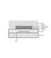
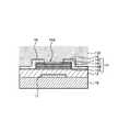
先ず、図1に示すように、絶縁性基板10上にゲート金属膜を成膜し、該ゲート金属膜をパターニングすることによりゲート電極11を形成した後で、ゲート電極11を覆うゲート絶縁膜(第1絶縁体)12を絶縁性基板10上に成膜する。 First, as shown in FIG. 1, after forming a gate metal film on the insulating
次に、大気に曝すことなく、図2に示すように、ゲート絶縁膜12に酸素プラズマ処理或いはその他の第1酸化性処理(酸化性処理)131を施す。 Next, as shown in FIG. 2, oxygen plasma treatment or other first oxidation treatment (oxidation treatment) 131 is performed on the
この第1酸化性処理131により、ゲート絶縁膜12の表面に酸素を付着させた状態にすることができるとともに、例えばゲート絶縁膜12の表層部において酸素欠損が生じていた場合に、その酸素欠損を解消することができる。 By this
第1酸化性処理131に引き続き、大気に曝すことなく、図3に示すようにゲート絶縁膜12上に酸化物半導体膜14を成膜する。 Following the
これにより、酸化物半導体膜14において、ゲート絶縁膜12との界面に位置する部分である第1界面層14Aは、予めゲート絶縁膜12の表面上に付着されていた酸素により酸化される。 Thereby, in the
よって、酸化物半導体膜14の第1界面層14Aの酸素空孔欠陥が低減化される。 Therefore, oxygen vacancy defects in the
すなわち、酸化物半導体膜14の第1界面層14Aの酸素空孔密度が、酸化物半導体膜14のバルク層14Bよりも小さくなる。 That is, the oxygen vacancy density of the
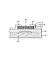
次に、図4に示すように、酸化物半導体膜14を所望の形状にパターニングする。 Next, as illustrated in FIG. 4, the
次に、図5に示すように、酸化物半導体膜14に還元性プラズマ処理或いはその他の還元性処理15を施す。 Next, as shown in FIG. 5, the
これにより、酸化物半導体膜14の表層部14Cには酸素空孔欠陥が積極的に形成される。 Thereby, oxygen vacancy defects are positively formed in the
すなわち、酸化物半導体膜14の表層部14Cの酸素空孔密度が、酸化物半導体膜14のバルク層14Bよりも大きくなる。 That is, the oxygen vacancy density in the
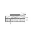
次に、図6に示すように、ゲート絶縁膜12及び酸化物半導体膜14上に亘ってソース・ドレイン金属膜を成膜し、該ソース・ドレイン金属膜をパターニングすることにより、ソース・ドレイン電極16(一方がソース電極で他方がドレイン電極)を形成する。 Next, as shown in FIG. 6, a source / drain metal film is formed over the
ここで、図5の還元性処理15とその後のソース・ドレイン金属膜の成膜も、引き続き、大気に曝すことなく連続して行うことが望ましい。 Here, it is desirable that the reducing
次に、図7に示すように、ソース・ドレイン電極16の間隔16Aを介して、酸化物半導体膜14に、酸素プラズマ処理或いはその他の第2酸化性処理(酸化性処理)132を施す。 Next, as shown in FIG. 7, an oxygen plasma treatment or other second oxidizing treatment (oxidizing treatment) 132 is performed on the
これにより、酸化物半導体膜14の表層部14C(図6参照)において、間隔16Aに位置する部分である第2界面層14Eは酸化されるため、該第2界面層14Eの酸素空孔欠陥が低減化される。 As a result, in the
すなわち、酸化物半導体膜14の第2界面層14Eの酸素空孔密度が、酸化物半導体膜14のバルク層14Bよりも小さくなる。 That is, the oxygen vacancy density of the
なお、酸化物半導体膜14の表層部14C(図6参照)において、酸化物半導体膜14の第2界面層14E以外の部分、すなわち、ソース・ドレイン電極16との界面に位置する部分は、第3界面層14Dを構成する。 Note that in the
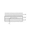
次に、図8に示すように、ソース・ドレイン電極16上を覆うとともに、ソース・ドレイン電極16の間隔16Aにおいては酸化物半導体膜14上を覆うように、保護絶縁膜(第2絶縁体)18を成膜する。 Next, as shown in FIG. 8, a protective insulating film (second insulator) is formed so as to cover the source /
これにより、薄膜トランジスタ100が製造される。 Thereby, the
なお、図7の第2酸化性処理132とその後の保護絶縁膜18の成膜も、引き続き、大気に曝すことなく連続して行うことが望ましい。 Note that it is desirable that the
ここで、酸化物半導体膜14において、ゲート絶縁膜12との界面に位置する部分である第1界面層14Aの酸素空孔密度は、例えば、1×10¹²〜1×1018cm−3である。Here, in the
また、酸化物半導体膜14のバルク層14Bの酸素空孔密度は、例えば、1×10¹⁶〜1×1020cm−3である。The oxygen vacancy density of the
第1界面層14A及びバルク層14Bの酸素空孔密度は、成膜条件を制御することにより実現できる。すなわち、成膜中における雰囲気中の酸素濃度を高めると、酸素空孔密度を小さくすることができる一方で、成膜中における雰囲気中の酸素濃度を低くすると酸素空孔密度を大きくすることができる。 The oxygen vacancy density of the
図2の酸化性処理13を行うので、第1界面層14Aの電子密度を適度に低減することができ、薄膜トランジスタ100をドレイン電流のオン・オフ比が5桁以上(1×10⁴以上)の良好なスイッチング特性のものとすることができる。2 is performed, the electron density of the
また、酸化物半導体膜14において、ソース・ドレイン電極16との界面に位置する部分である第3界面層14Dの酸素空孔密度は、例えば、1×10¹⁹〜1×1022cm−3である。In the
また、酸化物半導体膜14において、保護絶縁膜18との界面に位置する部分である第2界面層14Eの酸素空孔密度は、例えば、1×10¹⁶〜1×1020cm−3である。In the
第3界面層14D及び第2界面層14Eの酸素空孔密度も、成膜条件を制御することにより実現できる。すなわち、成膜中における雰囲気中の酸素濃度を高めると、酸素空孔密度を小さくすることができる一方で、成膜中における雰囲気中の酸素濃度を低くすると酸素空孔密度を大きくすることができる。 The oxygen vacancy density of the
図5の還元性処理15を行うので、第3界面層14Dの電子密度を適度に増加させることができ、該第3界面層14Dにオーミックコンタクト層としての機能を持たせることができる。 Since the reducing
また、図7の酸化性処理13を行うので、第2界面層14Eの電子密度を適度に低減することができ、バックチャネル電子電流に起因するオフ電流を効率よく低減化する機能を持たせることができる。 In addition, since the oxidation treatment 13 of FIG. 7 is performed, the electron density of the
以上のような第1の実施形態によれば、ゲート電極11と、ゲート絶縁膜(第1絶縁体)12と、酸化物半導体膜14と、ソース・ドレイン金属16と、保護絶縁膜(第2絶縁体)18と、がこの順に成膜されてなる積層構造を備える薄膜トランジスタ100の酸化物半導体膜14と絶縁膜12、18との界面における酸素空孔起因の欠陥(過剰電子ドナーを生成する欠陥)を制御できる。 According to the first embodiment as described above, the
即ち、欠陥が必要な箇所には積極的に生成でき、不要な箇所では抑制できる。 That is, it can be actively generated at a place where a defect is necessary, and can be suppressed at an unnecessary place.
具体的には、図2に示す第1酸化性処理131を行った後で図3に示すように酸化物半導体膜14を成膜することにより、該酸化物半導体膜14においてゲート絶縁膜12との界面に位置する界面層14Aの酸素空孔欠陥を低減化できる。すなわち、界面層14Aの酸素空孔密度をバルク層14Bよりも小さくすることができる。 Specifically, after the
また、図5に示す還元性処理15を行うことにより、酸化物半導体膜14の表層部14C(具体的には、表層部14Cにおいて、ソース・ドレイン電極16との界面に位置することになる第3界面層14D(図7、図8))に酸素空孔欠陥を積極的に形成し、この欠陥を電子ドナーとして作用させることによって、ソース・ドレイン電極16との界面に位置する第3界面層14Dをよりn型化し、オーミックコンタクト接合を形成しやすくすることができる。 Further, by performing the reducing
また、図7に示す第2酸化性処理132を行うことにより、酸化物半導体膜14の表層部14Cにおいて、ソース・ドレイン領域以外(開口16A内)の部分である第2界面層14Eの酸素空孔欠陥を低減化し、薄膜トランジスタ100のオフ電流の低減化を実現することができる。 Further, by performing the
〔第2の実施形態〕
図9乃至図14は、第1の実施形態に係る薄膜トランジスタ(薄膜デバイス)200(図14)の製造方法を示す一連の工程図である。[Second Embodiment]
9 to 14 are a series of process diagrams showing a method of manufacturing the thin film transistor (thin film device) 200 (FIG. 14) according to the first embodiment.
本実施形態に係る薄膜トランジスタ200は、トップゲートスタガ型の薄膜トランジスタである。 The
以下、製造方法について説明する。 Hereinafter, the manufacturing method will be described.
先ず、図9に示すように、絶縁性基板10上に下地絶縁膜(第1絶縁体)21を成膜した後で、該下地絶縁膜21上にソース・ドレイン金属膜を成膜し、該ソース・ドレイン金属膜をパターニングすることによりソース・ドレイン電極16(一方がソース電極で他方がドレイン電極)を形成する。 First, as shown in FIG. 9, after a base insulating film (first insulator) 21 is formed on the insulating
次に、図10に示すように、酸素プラズマ処理或いはその他の第1酸化性処理131を施す。 Next, as shown in FIG. 10, oxygen plasma treatment or other
この第1酸化性処理131により、下地絶縁膜21の表面に酸素を付着させた状態にすることができるとともに、例えば下地絶縁膜21の表層部において酸素欠損が生じていた場合に、その酸素欠損を解消することができる。 By this
次に、下地絶縁膜21上及びソース・ドレイン電極16上に酸化物半導体膜14を成膜した後で、該酸化物半導体膜14を、図11に示すように所望の形状にパターニングする。 Next, after forming the
ここで、酸化物半導体膜14において、下地絶縁膜21との界面に位置する部分である第1界面層14Aは、予め下地絶縁膜21の表面上に付着されていた酸素により酸化される。 Here, in the
よって、酸化物半導体膜14の第1界面層14Aの酸素空孔欠陥が低減化される。 Therefore, oxygen vacancy defects in the
すなわち、第1界面層14Aの酸素空孔密度が、酸化物半導体膜14のバルク層14Bよりも小さくなる。 That is, the oxygen vacancy density of the
なお、図10の酸化性処理13と、酸化物半導体膜14の成膜とは、大気に曝すことなく、連続して行うことが好ましい。 Note that the oxidizing treatment 13 and the formation of the
次に、図12に示すように、酸化物半導体膜14に酸素プラズマ処理或いはその他の第2酸化性処理132を施す。 Next, as shown in FIG. 12, the
これにより、酸化物半導体膜14の第2界面層14Eは酸化されるため、該第2界面層14Eの酸素空孔欠陥が低減化される。 As a result, the
すなわち、第2界面層14Eの酸素空孔密度が、酸化物半導体膜14のバルク層14Bよりも小さくなる。 That is, the oxygen vacancy density of the
次に、大気に曝すことなく引き続いて、図13に示すように、酸化物半導体膜14を覆うゲート絶縁膜(第2絶縁体)12をソース・ドレイン電極16上に成膜する。 Next, as shown in FIG. 13, a gate insulating film (second insulator) 12 covering the
次に、図14に示すように、ゲート絶縁膜12上にゲート電極11を形成した後で、該ゲート電極11を覆う保護絶縁膜18をゲート絶縁膜12上に形成する。 Next, as shown in FIG. 14, after forming the
これにより、薄膜トランジスタ200が製造される。 Thereby, the
以上のような第2の実施形態によれば、下地絶縁膜(第1絶縁体)21と、ソース・ドレイン電極16と、酸化物半導体膜14と、ゲート絶縁膜(第2絶縁体)12と、ゲート電極11と、保護絶縁膜18と、がこの順に成膜されてなる積層構造を備える薄膜トランジスタ200の酸化物半導体膜14と絶縁膜21,12との界面における酸素空孔起因の欠陥を制御できる。 According to the second embodiment as described above, the base insulating film (first insulator) 21, the source /
具体的には、図10に示す第1酸化性処理131を行った後で図11に示すように酸化物半導体膜14を成膜することにより、該酸化物半導体膜14において下地絶縁膜21との界面に位置する界面層14Aの酸素空孔欠陥を低減化できる。すなわち、界面層14Aの酸素空孔密度をバルク層14Bよりも小さくすることができる。 Specifically, after the
また、図12に示す第2酸化性処理131を行うことにより、酸化物半導体膜14において、ゲート絶縁膜12との界面に位置することになる第2界面層14Eの酸素空孔欠陥を低減化することにより該第2界面層14Eの電子密度を適度に低減し、バックチャネル電子電流に起因する薄膜トランジスタ200のオフ電流を効率よく低減化することができる。 In addition, by performing the
〔第3の実施形態〕
図15乃至図19は、第3の実施形態に係る薄膜トランジスタ(薄膜デバイス)300(図19)の製造方法を示す一連の工程図である。[Third Embodiment]
15 to 19 are a series of process diagrams showing a method of manufacturing the thin film transistor (thin film device) 300 (FIG. 19) according to the third embodiment.
本実施形態に係る薄膜トランジスタ300は、トップゲートプレーナ型の薄膜トランジスタである。 The
以下、製造方法について説明する。 Hereinafter, the manufacturing method will be described.
先ず、図15に示すように、絶縁性基板10上に下地絶縁膜(第1絶縁体)21を成膜した後で、該下地絶縁膜21に対して酸素プラズマ処理或いはその他の第1酸化性処理131を施す。 First, as shown in FIG. 15, after a base insulating film (first insulator) 21 is formed on the insulating
その後、大気に曝すことなく、下地絶縁膜21上に酸化物半導体膜14を成膜する(図16参照)。 After that, the
ここで、酸化物半導体膜14において、下地絶縁膜21との界面に位置する部分である第1界面層14Aは、予め下地絶縁膜21の表面上に付着されていた酸素により酸化される。 Here, in the
よって、酸化物半導体膜14の第1界面層14Aの酸素空孔欠陥が低減化される。 Therefore, oxygen vacancy defects in the
すなわち、第1界面層14Aの酸素空孔密度が、酸化物半導体膜14のバルク層14Bよりも小さくなる。 That is, the oxygen vacancy density of the
更に、図16に示すように、酸化物半導体膜14を所望の形状にパターニングする。 Further, as shown in FIG. 16, the
更に、図16に示すように、酸化物半導体膜14に酸素プラズマ処理或いはその他の第2酸化性処理132を施す。 Further, as shown in FIG. 16, the
これにより、酸化物半導体膜14の第2界面層14Eは酸化されるため、該第2界面層14Eの酸素空孔欠陥が低減化される。 As a result, the
すなわち、第2界面層14Eの酸素空孔密度が、酸化物半導体膜14のバルク層14Bよりも小さくなる。 That is, the oxygen vacancy density of the
次に、大気に曝すことなく、図17に示すように、酸化物半導体膜14を覆うゲート絶縁膜(第2絶縁体)12を下地絶縁膜21上に成膜し、更に、ゲート絶縁膜12上にゲート電極11を形成する。 Next, as shown in FIG. 17, a gate insulating film (second insulator) 12 that covers the
次に、図18に示すように、ゲート電極11を覆う層間絶縁膜23をゲート絶縁膜12上に成膜した後で、ソース・ドレイン領域へのコンタクトホール19を層間絶縁膜23及びゲート絶縁膜12に亘って形成する。 Next, as shown in FIG. 18, after an
次に、図19に示すように、コンタクトホール19内からゲート絶縁膜12上に亘るソース・ドレイン電極16(一方がソース電極で他方がドレイン電極)を形成した後で、該ソース・ドレイン電極16を覆う保護絶縁膜18を層間絶縁膜23上に成膜する。 Next, as shown in FIG. 19, after forming the source / drain electrode 16 (one is a source electrode and the other is a drain electrode) from the
これにより、薄膜トランジスタ300が製造される。 Thereby, the
以上のような第3の実施形態によれば、下地絶縁膜(第1絶縁体)21と、酸化物半導体膜14と、ゲート絶縁膜(第2絶縁体)12と、ゲート電極11と、層間絶縁膜23と、ソース・ドレイン金属膜16と、保護絶縁膜18と、がこの順に成膜されてなる積層構造を備える薄膜トランジスタ300の酸化物半導体膜14と絶縁膜21,12との界面における酸素空孔起因の欠陥(過剰電子ドナーを生成する欠陥)を制御できる。 According to the third embodiment as described above, the base insulating film (first insulator) 21, the
具体的には、図15に示す第1酸化性処理131を行った後で図16に示すように酸化物半導体膜14を成膜することにより、該酸化物半導体膜14において下地絶縁膜21との界面に位置する界面層14Aの酸素空孔欠陥を低減化できる。すなわち、界面層14Aの酸素空孔密度をバルク層14Bよりも小さくすることができる。 Specifically, after the
また、図16に示す第2酸化性処理132を行うことにより、酸化物半導体膜14において、ゲート絶縁膜12との界面に位置することになる第2界面層14Eの酸素空孔欠陥を低減化することにより該第2界面層14Eの電子密度を適度に低減し、バックチャネル電子電流に起因する薄膜トランジスタ300のオフ電流を効率よく低減化することができる。 In addition, by performing the
〔第4の実施形態〕
図20乃至図24は、第4の実施形態に係る薄膜トランジスタ(薄膜デバイス)400の製造方法を示す一連の工程図である。[Fourth Embodiment]
20 to 24 are a series of process diagrams showing a method of manufacturing a thin film transistor (thin film device) 400 according to the fourth embodiment.
本実施形態に係る薄膜トランジスタ400は、ボトムゲートプレーナ型の薄膜トランジスタである。 The
以下、製造方法について説明する。 Hereinafter, the manufacturing method will be described.
先ず、図20に示すように、絶縁性基板10上にゲート金属膜を成膜し、該ゲート金属膜をパターニングすることによりゲート電極11を形成し、このゲート電極11を覆うゲート絶縁膜(第1絶縁体)12を絶縁性基板10上に成膜する。 First, as shown in FIG. 20, a gate metal film is formed on the insulating
次に、図21に示すように、ゲート絶縁膜12上にソース・ドレイン金属膜を成膜し、該ソース・ドレイン金属膜をパターニングすることにより、ソース・ドレイン電極16(一方がソース電極で他方がドレイン電極)を形成し、ソース・ドレイン電極16の間隔16Aを介して、ゲート絶縁膜12に酸素プラズマ処理或いはその他の第1酸化性処理131を施す。 Next, as shown in FIG. 21, a source / drain metal film is formed on the
この第1酸化性処理131により、ゲート絶縁膜12の表面に酸素を付着させた状態にすることができるとともに、例えばゲート絶縁膜12の表層部において酸素欠損が生じていた場合に、その酸素欠損を解消することができる。 By this
第1酸化性処理131に引き続き、大気に曝すことなく、図22に示すようにゲート絶縁膜12上に酸化物半導体膜14を成膜し、所望の形状にパターニングする。 Subsequent to the
これにより、酸化物半導体膜14において、ゲート絶縁膜12との界面に位置する部分である第1界面層14Aは、予めゲート絶縁膜12の表面上に付着されていた酸素により酸化される。 Thereby, in the
よって、酸化物半導体膜14の第1界面層14Aの酸素空孔欠陥が低減化される。 Therefore, oxygen vacancy defects in the
すなわち、酸化物半導体膜14の第1界面層14Aの酸素空孔密度が、酸化物半導体膜14のバルク層14Bよりも小さくなる。 That is, the oxygen vacancy density of the
次に、図23に示すように、酸化物半導体膜14に酸素プラズマ処理或いはその他の第2酸化性処理132を施す。 Next, as illustrated in FIG. 23, the
引き続いて、大気に曝すことなく、図24に示すように、酸化物半導体膜14を覆う保護絶縁膜(第2絶縁体)18をソース・ドレイン電極16上に成膜する。 Subsequently, as shown in FIG. 24, a protective insulating film (second insulator) 18 covering the
これにより、薄膜トランジスタ400が製造される。 Thereby, the
以上のような第4の実施形態によれば、ゲート電極11と、ゲート絶縁膜(第1絶縁体)12と、ソース・ドレイン電極16と、酸化物半導体膜14と、保護絶縁膜(第2絶縁体)18と、がこの順に成膜されてなる積層構造を備える薄膜トランジスタ400の酸化物半導体膜14と絶縁膜12,18との界面における酸素空孔起因の欠陥(過剰電子ドナーを生成する欠陥)を制御できる。 According to the fourth embodiment as described above, the
具体的には、図21に示す第1酸化性処理131を行った後で図22に示すように酸化物半導体膜14を成膜することにより、該酸化物半導体膜14においてゲート絶縁膜12との界面に位置する界面層14Aの酸素空孔欠陥を低減化できる。すなわち、界面層14Aの酸素空孔密度をバルク層14Bの酸素空孔密度よりも小さくすることができる。 Specifically, after the
また、図23に示す第2酸化性処理131を行うことにより、酸化物半導体膜14において、保護絶縁膜18との界面に位置することになる第2界面層14Eの酸素空孔欠陥を低減化することにより該第2界面層14Eの電子密度を適度に低減し、バックチャネル電子電流に起因する薄膜トランジスタ400のオフ電流を効率よく低減化することができる。 In addition, by performing the
〔第5の実施形態〕
上記の第1乃至第4の実施形態では、薄膜トランジスタ100、200、300、400の酸化物半導体膜14を一度に成膜する例を説明したが、第5の実施形態では、酸化物半導体膜14を複数層に分けて成膜する例を説明する。[Fifth Embodiment]
In the first to fourth embodiments, the example in which the
以下、本実施形態の場合の酸化物半導体膜14の成膜方法について説明する。 Hereinafter, a method for forming the
先ず、図25に示すように、第1絶縁体50上に非常に薄い酸化物半導体膜51を成膜する。ここで、第1絶縁体50は、例えば、第1の実施形態(図8)及び第4の実施形態(図24)ではゲート絶縁膜12に相当し、第2の実施形態(図14)及び第3の実施形態(図19)では下地絶縁膜21に相当する。 First, as shown in FIG. 25, a very thin
次に、図26に示すように、酸化物半導体膜51に酸素プラズマ処理或いはその他の酸化性処理52を施す。 Next, as illustrated in FIG. 26, the
これにより、酸化物半導体膜51の表層部が酸化される。 Thereby, the surface layer portion of the
次に、図27に示すように、酸化物半導体膜51上に、非常に薄い酸化物半導体膜51を成膜する。 Next, as illustrated in FIG. 27, a very thin
次に、図28に示すように、酸化物半導体膜51に酸化性処理52を施す。 Next, as illustrated in FIG. 28, the
次に、図29に示すように、酸化物半導体膜51上に、非常に薄い酸化物半導体膜51を成膜する。 Next, as illustrated in FIG. 29, a very thin
更に、必要に応じた回数だけ、図26及び図27の処理を繰り返し行うことにより、酸化物半導体膜14を形成する。 Further, the
以上のような第5の実施形態によれば、酸化物半導体膜(酸化物半導体薄層)51の成膜と、酸化性処理52と、を交互に複数回繰り返すことにより、酸化物半導体膜14を形成するので、各酸化物半導体薄層51を充分に酸化でき、所望の膜質の酸化物半導体膜14を精度良く得ることができる。 According to the fifth embodiment as described above, the
なお、上記の第1乃至第5の実施形態において、酸化物半導体膜14としては、例えば、少なくともZn、Ga、Inのいずれか一元素を含む非晶質酸化物又は結晶酸化物を用いることができる。このような酸化物半導体膜14は、例えば、スパッタ、蒸着、CVDなどにより形成可能である。特に、結晶酸化物膜の酸化物半導体膜14は、非晶質膜にXeClエキシマレーザ或いはその他のレーザを照射することにより形成することができる。これらの酸化物半導体膜14は、例えば、可視光に対してはほぼ透明であるが、波長308nmのXeClエキシマレーザに対しては不透明であり吸収するからである。もちろん、その他の可視光よりも短波長なレーザや光を照射することによっても結晶化できる。また、これらの酸化物半導体膜14は、粒子状の酸化物半導体を溶媒に溶かしその酸化物半導体溶液を塗布又は印刷しその後加熱処理で溶媒を蒸発させることによっても形成することができる。 In the first to fifth embodiments described above, as the
また第1乃至第5の実施形態における酸化性処理又は還元性処理に関しては、酸化性プラズマ処理又は還元性プラズマ処理が適用できる。酸化性プラズマ処理としては、少なくとも酸素プラズマ又はオゾンプラズマを含むプラズマ処理が可能である。また還元性プラズマ処理としては、ArやHeなどの希ガスプラズマ、水素プラズマ、窒素ガスプラズマ或いはこれらのうちの任意の組み合わせの混合ガスプラズマを用いるプラズマ処理が可能である。 In addition, regarding the oxidizing treatment or reducing treatment in the first to fifth embodiments, an oxidizing plasma treatment or a reducing plasma treatment can be applied. As the oxidizing plasma treatment, plasma treatment including at least oxygen plasma or ozone plasma is possible. As the reducing plasma treatment, plasma treatment using rare gas plasma such as Ar or He, hydrogen plasma, nitrogen gas plasma, or a mixed gas plasma of any combination thereof is possible.
なお、上記の各実施形態では、第1絶縁体(上記の各実施形態ではゲート絶縁膜12又は下地絶縁膜21)と第2絶縁体(上記の各実施形態では保護絶縁膜18又はゲート絶縁膜12)に挟まれた酸化物半導体膜14において、第1絶縁体との界面に位置する部分である第1界面層14Aと、第2絶縁体との界面に位置する部分である第2界面層14Eと、の双方が、バルク層14Bの酸素空孔密度よりも小さい例を説明したが、所望の薄膜トランジスタの構成に応じては、第1界面層14Aと第2界面層14Eのうちの何れか一方のみの酸素空孔密度が、バルク層14Bの酸素空孔密度よりも小さいようにしても良い。 In each of the above embodiments, the first insulator (the
更に、上記の各実施形態では、第1絶縁体としてのゲート絶縁膜12又は下地絶縁膜21を絶縁性基板10上に成膜する例を説明したが、本発明はこの例に限らず、絶縁性基板10を第1絶縁体として利用する場合もある。但し、歩留まりや特性安定性を考慮すると、絶縁性基板10上に第1絶縁体(例えば、ゲート絶縁膜12或いは下地絶縁膜21)を成膜することが好ましい。 Further, in each of the above embodiments, the example in which the
また、上記の各実施形態では、薄膜デバイスとして薄膜トランジスタ100,200,300,400を例示したが、本発明はこの例に限らず、薄膜ダイオードにも適用可能である。 In each of the above embodiments, the
図1乃至図8を参照して実施例1を説明する。 A first embodiment will be described with reference to FIGS.
先ず、図1に示すように、絶縁性基板10としてのガラス基板上に、ゲート金属膜としてのCr金属膜をスパッタ法により成膜した後で、通常のフォトリソ工程を用いてCr金属膜を所望のゲート電極11の形状にパターニングした。 First, as shown in FIG. 1, a Cr metal film as a gate metal film is formed on a glass substrate as an insulating
その後、ゲート絶縁膜12としての窒化シリコン膜を300nmの膜厚にスパッタ法により成膜した。 Thereafter, a silicon nitride film as the
その後、大気に曝すことなく、図2に示すようにゲート絶縁膜12を酸素プラズマに曝して第1酸化性処理131を行うことにより窒化シリコン膜の表面を酸化した。 Thereafter, the surface of the silicon nitride film was oxidized by performing the
更に引き続いて大気に曝すことなくスパッタ法によりInGaZnO4からなる酸化物半導体膜14を100nm成膜した(図3)。Further, an
スパッタのターゲットとしては、InGaZnO4の焼結体を用いたが、In、Ga、Znそれぞれの金属の酸化物を個別にターゲットとしてスパッタを行い基板上で反応させることによりInGaZnO4化合物を形成しても良い。As a sputtering target, a sintered body of InGaZnO4 was used, but an InGaZnO4 compound was formed by sputtering and reacting on the substrate with oxides of respective metals of In, Ga and Zn individually. Also good.
以上のゲート窒化シリコン膜成膜、酸素プラズマ処理、InGaZnO4酸化物半導体膜14の成膜を、例えば、真空状態(減圧状態)の同一のスパッタ装置で行うことにより、大気に曝すことなくこれらの工程を連続して行うことができる。The above-described gate silicon nitride film formation, oxygen plasma treatment, and InGaZnO4
その後、酸化物半導体膜14を通常のフォトリソ工程を用いて所望のアイランド形状にパターニングした(図4)。 After that, the
引き続いて、還元性処理15として酸化物半導体膜14をArプラズマに曝した(図5)。 Subsequently, the
このようにArプラズマに曝すことにより酸化物半導体膜14の表層部14Cに酸素空孔が形成され、酸化物半導体膜14の表面層14Cの抵抗率値が処理前の値の1/100000程度まで低下し、ソース・ドレイン領域として適切な値となった。 By exposing to Ar plasma in this manner, oxygen vacancies are formed in the
このArプラズマ処理の後、大気に曝すことなく連続してソース・ドレイン用金属としてCr膜を成膜し、所望の形状にパターニングすることによりソース・ドレイン電極16を形成した(図6)。 After this Ar plasma treatment, a Cr film was continuously formed as a source / drain metal without being exposed to the atmosphere, and a source /
更に、ソース・ドレイン電極16の間隔16Aを介して、酸化物半導体膜14の表面層14Cを酸素プラズマに曝して第2酸化性処理132を行った(図7)。 Further, the
この酸素プラズマ処理は、ソース・ドレイン電極16間の酸化物半導体膜14の表層部(第2界面層14E)を酸化し酸素空孔に起因する過剰ドナー電子を低減化させる目的で行う。このように酸素空孔を減らすことにより、薄膜トランジスタ100のオフ電流値を2桁程度低減化させることができた。 This oxygen plasma treatment is performed for the purpose of oxidizing the surface layer portion (
その後、大気に曝すことなく連続して、保護絶縁膜18として窒化シリコン膜を300nmスパッタ法により成膜した。 Thereafter, a silicon nitride film was continuously formed as the protective insulating
以上のプロセスにより薄膜トランジスタ100が得られた(図8)。 Through the above process, the
次に、図9乃至14を参照して実施例2を説明する。 Next, Embodiment 2 will be described with reference to FIGS.
絶縁性基板10としての樹脂基板上に、スパッタ法により下地絶縁膜21としての窒化シリコン膜を300nm成膜した後、Mo金属膜を成膜し、その後通常のフォトリソ工程を用いて、該Mo金属膜を所望の形状にパターニングすることにより、ソース・ドレイン電極16を形成した(図9)。 On the resin substrate as the insulating
引き続き、第1酸化性処理131として、ソース・ドレイン電極16の間隔16Aを介して下地絶縁膜21を酸素プラズマに曝す処理を行った(図10)。 Subsequently, as the
引き続き、大気に曝すことなく連続してInGaZnO4からなる酸化物半導体成膜14をスパッタ法により室温で60nmの膜厚に成膜し、該酸化物半導体膜14を所望のアイランド形状にパターニングした(図11)。Subsequently, an
その後、酸化物半導体膜14の表層部(第2界面層14E)を第2酸化性処理132として酸素プラズマに曝し、該表層部を酸化させ該表層部の酸素空孔を低減化させた(図12)。 After that, the surface layer portion (
その後、大気に曝すことなく連続してゲート絶縁膜12としての窒化シリコン膜をスパッタ法により400nm成膜した(図13)。 Thereafter, a silicon nitride film as the
その後、ゲート電極11をAlで形成し、保護絶縁膜18としての窒化シリコン膜をスパッタ法により300nm成膜することにより、薄膜トランジスタ200が得られた(図14)。 Thereafter, the
上記のような酸素プラズマ処理を行うことにより薄膜トランジスタのチャネル領域の電子密度の制御が良好となり、ドレイン電流のオン・オフ比が5桁以上の良好なスイッチング特性が実現できた。 By performing the oxygen plasma treatment as described above, the electron density in the channel region of the thin film transistor was well controlled, and good switching characteristics with a drain current on / off ratio of 5 digits or more were realized.
より良好な特性を得るためには、酸化物半導体膜14を60nmの膜厚に成膜した後、連続して酸素プラズマ処理を行い、更に連続して、窒化シリコンからなるゲート絶縁膜12の一部(膜厚50nm:第1ゲート絶縁膜)を成膜する。 In order to obtain better characteristics, after the
その後、この第1ゲート絶縁膜と酸化物半導体膜14の積層膜を所望のアイランド形状にパターニングし、更に窒化シリコンからなるゲート絶縁膜12の残りの一部(膜厚350nm:第2ゲート絶縁膜)を成膜する。 Thereafter, the laminated film of the first gate insulating film and the
このような方法により形成される薄膜トランジスタ200のゲート絶縁膜厚は400nmとなり上記の場合と同じであるが、重要な相違点は酸化物半導体膜14とゲート絶縁膜12との界面が大気に一度も曝されないという点である(上述の場合には、酸化物半導体膜14のパターニングの際にこの酸化物半導体膜14の上面が大気やフォトリソプロセスに曝されることになる)。 The gate insulating film thickness of the
このように酸化物半導体膜14と絶縁膜(例えば、ゲート絶縁膜12)との界面を大気に曝されないようにすると、酸素空孔欠陥やその他の不純物欠陥の生成を抑制することができ、非常に良好なスイッチング特性が実現できる。 In this manner, when the interface between the
次に、図15乃至図19を参照して実施例3を説明する。 Next, Embodiment 3 will be described with reference to FIGS.
絶縁性基板10としてのガラス基板上にスパッタ法により下地絶縁膜21としての窒化シリコン膜を300nm成膜し、該下地膜絶縁膜21の表面に酸素プラズマに曝して第1酸化性処理131を行うことにより窒化シリコン膜の表面を酸化した(図15)。 A 300 nm silicon nitride film as a
その後、InGaZnO4からなる酸化物半導体成膜14をスパッタ法により室温で60nmの膜厚に成膜した。この室温成膜の非晶質の酸化物半導体膜14にXeClエキシマレーザを照射して溶融・固化させることにより結晶化させた。その後、この多結晶の酸化物半導体膜14を所望のアイランド形状にパターニングした。引き続き、酸素プラズマ処理(第2酸化性処理132)により多結晶の酸化物半導体膜14の表層部(第2界面層14E)を酸化させ酸素空孔欠陥を低減化させた(図16)。Thereafter, an
InGaZnO4からなる酸化物半導体成膜14をレーザ照射により結晶化させる場合、非常に高温な溶融状態において酸素が抜けてしまうので、この酸素プラズマ処理は非常に重要である。When the
酸素プラズマ処理の後、大気に曝すことなく連続してゲート絶縁膜12としての窒化シリコン膜をスパッタ法により100nm成膜した。更にAlを用いてゲート電極11を形成した(図17)。 After the oxygen plasma treatment, a silicon nitride film as a
引き続き、層間絶縁膜23としての酸化シリコン膜を400nm成膜し、ソース・ドレイン電極用のコンタクトホール19を形成した(図18)。 Subsequently, a 400 nm silicon oxide film as an
次に、Alを用いてソース・ドレイン電極16を形成した後、保護絶縁膜18としての窒化シリコン膜を300nm成膜して薄膜トランジスタ300が得られた。 Next, after forming the source /
実施例3では、実施例1,2の場合と比べて、酸化物半導体膜14を結晶化させたので、5〜10倍程度高い電子移動度が得られた。 In Example 3, since the
本発明の産業上の利用可能性としては、液晶ディスプレイや有機ELディスプレイなどのフラットパネルディスプレイの画素駆動素子が挙げられる。特に酸化物半導体は透明であるので、液晶ディスプレイの画素駆動素子に応用した場合、従来のシリコン半導体を用いた場合よりもバックライトからの透過光量が多くなり、より明るい高性能ディスプレイの実現が可能となる。このような駆動素子としては、3端子である薄膜トランジスタに限らず、2端子の薄膜ダイオードでも良い。 Industrial applicability of the present invention includes pixel drive elements for flat panel displays such as liquid crystal displays and organic EL displays. In particular, oxide semiconductors are transparent, so when applied to pixel drive elements for liquid crystal displays, the amount of light transmitted from the backlight is greater than when using conventional silicon semiconductors, enabling a brighter high-performance display. It becomes. Such a driving element is not limited to a three-terminal thin film transistor, and may be a two-terminal thin film diode.
また、酸化物半導体膜は、室温成膜した場合でも、従来の典型的な300℃成膜の非晶質シリコンよりも1桁程度電子移動度が高いので、室温成膜でも良好な特性を有する薄膜トランジスタアレイの形成が可能である。特に本発明の酸化性又は還元性プラズマ処理を用いることにより、薄膜トランジスタの電気特性を支配する酸化物半導体界面領域の酸素空孔密度を低温プロセスで制御可能である。従って、耐熱性の低い樹脂基板上でも良好な特性が得られるので、フレキシブル樹脂基板ディスプレイへの応用も可能である。 In addition, even when an oxide semiconductor film is formed at room temperature, it has an electron mobility that is about an order of magnitude higher than that of a conventional typical amorphous silicon film formed at 300 ° C., and thus has excellent characteristics even at room temperature. A thin film transistor array can be formed. In particular, by using the oxidizing or reducing plasma treatment of the present invention, the oxygen vacancy density in the oxide semiconductor interface region that governs the electrical characteristics of the thin film transistor can be controlled by a low temperature process. Accordingly, good characteristics can be obtained even on a resin substrate having low heat resistance, and therefore, application to a flexible resin substrate display is possible.
10 絶縁性基板
11 ゲート電極
12 ゲート絶縁膜
131 第1酸化性処理
132 第2酸化性処理
14 酸化物半導体
14A 第1界面層
14E 第2界面層
14B バルク層
15 還元性処理
16 ソース・ドレイン電極
18 保護絶縁膜
19 コンタクトホール
21 下地絶縁膜
23 層間絶縁膜
50 絶縁膜
100 薄膜トランジスタ(薄膜デバイス)
200 薄膜トランジスタ(薄膜デバイス)
300 薄膜トランジスタ(薄膜デバイス)
400 薄膜トランジスタ(薄膜デバイス)DESCRIPTION OF
200 Thin film transistor (thin film device)
300 Thin Film Transistor (Thin Film Device)
400 Thin film transistor
Claims (23)
Translated fromJapanese前記酸化物半導体膜において、前記第1絶縁体との界面に位置する部分である第1界面層と、前記第2絶縁体との界面に位置する部分である第2界面層と、のうちの少なくとも何れか一方の酸素空孔密度が、前記酸化物半導体膜において前記第1及び第2界面層以外の部分であるバルク層の酸素空孔密度よりも小さいことを特徴とする薄膜デバイス。In a thin film device having a laminated structure including a first insulator, an oxide semiconductor film, and a second insulator in this order, and an active layer formed of the oxide semiconductor film,
Of the oxide semiconductor film, a first interface layer that is a portion located at an interface with the first insulator and a second interface layer that is a portion located at an interface with the second insulator A thin film device, wherein at least one oxygen vacancy density is lower than an oxygen vacancy density of a bulk layer which is a portion other than the first and second interface layers in the oxide semiconductor film.
前記第1絶縁体、前記第2絶縁体及び前記酸化物半導体膜の成膜工程とは別に、酸化性処理を行うことにより、前記酸化物半導体膜において、前記第1絶縁体との界面に位置する部分である第1界面層と、前記第2絶縁体との界面に位置する部分である第2界面層と、のうちの少なくとも何れか一方の酸素空孔密度を、前記酸化物半導体膜において前記第1及び第2界面層以外の部分であるバルク層の酸素空孔密度よりも小さくすることを特徴とする薄膜デバイスの製造方法。By performing the step of forming an oxide semiconductor film on the first insulator and the step of forming a second insulator on the oxide semiconductor film, the first insulator, the oxide semiconductor film, and the first In a method of manufacturing a thin film device having a laminated structure including two insulators and having an active layer formed of the oxide semiconductor film,
In addition to the step of forming the first insulator, the second insulator, and the oxide semiconductor film, the oxide semiconductor film is positioned at the interface with the first insulator by performing an oxidation treatment. The oxygen vacancy density of at least one of the first interface layer, which is a portion to be formed, and the second interface layer, which is a portion located at the interface with the second insulator, in the oxide semiconductor film A method of manufacturing a thin film device, wherein the oxygen vacancy density of a bulk layer which is a portion other than the first and second interface layers is made smaller.
前記酸化物半導体膜は、酸化物半導体薄層の成膜と、酸化性処理と、を交互に複数回繰り返すことにより形成し、
前記酸化物半導体膜において、前記第1絶縁体との界面に位置する部分である第1界面層と、前記第2絶縁体との界面に位置する部分である第2界面層と、のうちの少なくとも何れか一方の酸素空孔密度を、前記酸化物半導体膜において前記第1及び第2界面層以外の部分であるバルク層の酸素空孔密度よりも小さくすることを特徴とする薄膜デバイスの製造方法。By performing the step of forming an oxide semiconductor film on the first insulator and the step of forming a second insulator on the oxide semiconductor film, the first insulator, the oxide semiconductor film, and the first In a method of manufacturing a thin film device having a laminated structure including two insulators and having an active layer formed of the oxide semiconductor film,
The oxide semiconductor film is formed by alternately repeating a film formation of an oxide semiconductor thin layer and an oxidizing treatment a plurality of times,
Of the oxide semiconductor film, a first interface layer that is a portion located at an interface with the first insulator and a second interface layer that is a portion located at an interface with the second insulator Manufacturing of a thin film device, characterized in that at least one oxygen vacancy density is made smaller than an oxygen vacancy density of a bulk layer other than the first and second interface layers in the oxide semiconductor film Method.
前記酸化物半導体膜は、酸化物半導体薄層の成膜と、酸化性処理と、を交互に複数回繰り返すことにより形成し、
前記第1絶縁体、前記第2絶縁体及び前記酸化物半導体膜の成膜工程とは別に、酸化性処理を行うことにより、前記酸化物半導体膜において、前記第1絶縁体との界面に位置する部分である第1界面層と、前記第2絶縁体との界面に位置する部分である第2界面層と、のうちの少なくとも何れか一方の酸素空孔密度を、前記酸化物半導体膜において前記第1及び第2界面層以外の部分であるバルク層の酸素空孔密度よりも小さくすることを特徴とする薄膜デバイスの製造方法。By performing the step of forming an oxide semiconductor film on the first insulator and the step of forming a second insulator on the oxide semiconductor film, the first insulator, the oxide semiconductor film, and the first In a method of manufacturing a thin film device having a laminated structure including two insulators and having an active layer formed of the oxide semiconductor film,
The oxide semiconductor film is formed by alternately repeating a film formation of an oxide semiconductor thin layer and an oxidizing treatment a plurality of times,
In addition to the step of forming the first insulator, the second insulator, and the oxide semiconductor film, the oxide semiconductor film is positioned at the interface with the first insulator by performing an oxidation treatment. The oxygen vacancy density of at least one of the first interface layer, which is a portion to be formed, and the second interface layer, which is a portion located at the interface with the second insulator, in the oxide semiconductor film A method of manufacturing a thin film device, wherein the oxygen vacancy density of a bulk layer which is a portion other than the first and second interface layers is made smaller.
前記ゲート絶縁膜の成膜後に、前記酸化性処理と、前記酸化物半導体膜の成膜と、を大気に曝すことなく、この順で連続して行うことを特徴とする請求項10乃至13の何れか一項に記載の薄膜デバイスの製造方法。The stacked structure of the thin film device includes a gate metal film, a gate insulating film as the first insulator, the oxide semiconductor film, a source / drain metal film, and a protective insulating film as the second insulator. And by forming a film in this order,
14. The oxidation treatment and the formation of the oxide semiconductor film are successively performed in this order after the formation of the gate insulating film without being exposed to the atmosphere. The manufacturing method of the thin film device as described in any one.
前記酸化物半導体膜を所望の形状にパターン形成した後で、還元性処理と、前記ソース・ドレイン金属膜の成膜と、を大気に曝すことなく、この順で連続して行うことを特徴とする請求項10乃至13の何れか一項に記載の薄膜デバイスの製造方法。The stacked structure of the thin film device includes a gate metal film, a gate insulating film as the first insulator, the oxide semiconductor film, a source / drain metal film, and a protective insulating film as the second insulator. And by forming a film in this order,
After the oxide semiconductor film is patterned into a desired shape, the reducing treatment and the formation of the source / drain metal film are continuously performed in this order without being exposed to the atmosphere. The method for manufacturing a thin film device according to any one of claims 10 to 13.
前記ソース・ドレイン金属膜を所望の形状にパターン形成した後で、前記酸化性処理と、前記保護絶縁膜の成膜と、を大気に曝すことなく、この順で連続して行うことを特徴とする請求項10乃至13の何れか一項に記載の薄膜デバイスの製造方法。The stacked structure of the thin film device includes a gate metal film, a gate insulating film as the first insulator, the oxide semiconductor film, a source / drain metal film, and a protective insulating film as the second insulator. And by forming a film in this order,
After forming the source / drain metal film in a desired shape, the oxidizing treatment and the formation of the protective insulating film are successively performed in this order without being exposed to the atmosphere. The method for manufacturing a thin film device according to any one of claims 10 to 13.
前記酸化物半導体膜の成膜後に、前記酸化性処理と、前記ゲート絶縁膜の成膜と、を大気に曝すことなく、この順で連続して行うことを特徴とする請求項10乃至13の何れか一項に記載の薄膜デバイスの製造方法。The stacked structure of the thin film device includes a base insulating film as the first insulator, a source / drain metal film, the oxide semiconductor film, a gate insulating film as the second insulator, and a gate metal film. And forming a protective insulating film in this order,
14. The film forming method according to claim 10, wherein after the oxide semiconductor film is formed, the oxidizing treatment and the gate insulating film are successively performed in this order without being exposed to the atmosphere. The manufacturing method of the thin film device as described in any one.
前記ソース・ドレイン金属膜を所望の形状にパターン形成した後で、前記酸化性処理又は前記還元性処理と、前記酸化物半導体膜の成膜と、を大気に曝すことなく、この順で連続して行うことを特徴とする請求項10乃至13の何れか一項に記載の薄膜デバイスの製造方法。The stacked structure of the thin film device includes a base insulating film as the first insulator, a source / drain metal film, the oxide semiconductor film, a gate insulating film as the second insulator, and a gate metal film. And forming a protective insulating film in this order,
After patterning the source / drain metal film into a desired shape, the oxidizing treatment or the reducing treatment and the formation of the oxide semiconductor film are continuously performed in this order without being exposed to the atmosphere. The method for manufacturing a thin film device according to claim 10, wherein the method is performed.
前記下地絶縁膜の成膜後に、前記酸化性処理と、前記酸化物半導体膜の成膜と、を大気に曝すことなく、この順で連続して行うことを特徴とする請求項10乃至13の何れか一項に記載の薄膜デバイスの製造方法。The stacked structure of the thin film device includes a base insulating film as the first insulator, the oxide semiconductor film, a gate insulating film as the second insulator, a gate metal film, an interlayer insulating film, A source / drain metal film and a protective insulating film are formed in this order,
14. The oxidation treatment and the formation of the oxide semiconductor film are successively performed in this order after the formation of the base insulating film without being exposed to the atmosphere. The manufacturing method of the thin film device as described in any one.
前記酸化物半導体膜の成膜後に、前記酸化性処理と、前記ゲート絶縁膜の成膜と、を大気に曝すことなく、この順に連続して行うことを特徴とする請求項10乃至13の何れか一項に記載の薄膜デバイスの製造方法。The stacked structure of the thin film device includes a base insulating film as the first insulator, the oxide semiconductor film, a gate insulating film as the second insulator, a gate metal film, an interlayer insulating film, A source / drain metal film and a protective insulating film are formed in this order,
14. The method according to claim 10, wherein after the formation of the oxide semiconductor film, the oxidizing treatment and the formation of the gate insulating film are sequentially performed in this order without being exposed to the atmosphere. A method for manufacturing a thin film device according to claim 1.
前記ソース・ドレイン金属膜を所望の形状にパターン形成後に、前記酸化性処理と、前記酸化物半導体膜の成膜と、を大気に曝すことなく、この順に連続して行うことを特徴とする請求項10乃至13の何れか一項に記載の薄膜デバイスの製造方法。The stacked structure of the thin film device includes a gate metal film, a gate insulating film as the first insulator, a source / drain metal film, the oxide semiconductor film, and a protective insulating film as the second insulator. And by forming a film in this order,
The patterning of the source / drain metal film is performed in a desired shape, and the oxidizing treatment and the formation of the oxide semiconductor film are successively performed in this order without being exposed to the atmosphere. Item 14. The method for manufacturing a thin film device according to any one of Items 10 to 13.
前記酸化物半導体膜を所望の形状にパターン形成後に、前記酸化性処理と、前記保護絶縁膜の成膜と、を大気に曝すことなく、この順に連続して行うことを特徴とする請求項10乃至13の何れか一項に記載の薄膜デバイスの製造方法。The stacked structure of the thin film device includes a gate metal film, a gate insulating film as the first insulator, a source / drain metal film, the oxide semiconductor film, and a protective insulating film as the second insulator. And by forming a film in this order,
11. The oxide semiconductor film is patterned in a desired shape, and then the oxidizing treatment and the formation of the protective insulating film are successively performed in this order without being exposed to the atmosphere. 14. The method for manufacturing a thin film device according to any one of items 1 to 13.
Priority Applications (5)
| Application Number | Priority Date | Filing Date | Title |
|---|---|---|---|
| JP2006217272AJP4609797B2 (en) | 2006-08-09 | 2006-08-09 | Thin film device and manufacturing method thereof |
| US11/890,426US7884360B2 (en) | 2006-08-09 | 2007-08-06 | Thin-film device and method of fabricating the same |
| US12/983,673US8420442B2 (en) | 2006-08-09 | 2011-01-03 | Method of fabricating a thin-film device |
| US13/837,879US8889480B2 (en) | 2006-08-09 | 2013-03-15 | Method of fabricating a thin-film device |
| US14/501,286US9209026B2 (en) | 2006-08-09 | 2014-09-30 | Method of fabricating a thin-film device |
Applications Claiming Priority (1)
| Application Number | Priority Date | Filing Date | Title |
|---|---|---|---|
| JP2006217272AJP4609797B2 (en) | 2006-08-09 | 2006-08-09 | Thin film device and manufacturing method thereof |
Related Child Applications (1)
| Application Number | Title | Priority Date | Filing Date |
|---|---|---|---|
| JP2009188007ADivisionJP5403464B2 (en) | 2009-08-14 | 2009-08-14 | Thin film device and manufacturing method thereof |
Publications (2)
| Publication Number | Publication Date |
|---|---|
| JP2008042088Atrue JP2008042088A (en) | 2008-02-21 |
| JP4609797B2 JP4609797B2 (en) | 2011-01-12 |
Family
ID=39051315
Family Applications (1)
| Application Number | Title | Priority Date | Filing Date |
|---|---|---|---|
| JP2006217272AActiveJP4609797B2 (en) | 2006-08-09 | 2006-08-09 | Thin film device and manufacturing method thereof |
Country Status (2)
| Country | Link |
|---|---|
| US (4) | US7884360B2 (en) |
| JP (1) | JP4609797B2 (en) |
Cited By (187)
| Publication number | Priority date | Publication date | Assignee | Title |
|---|---|---|---|---|
| JP2008072025A (en)* | 2006-09-15 | 2008-03-27 | Canon Inc | Field effect transistor and manufacturing method thereof |
| JP2008130814A (en)* | 2006-11-21 | 2008-06-05 | Canon Inc | Thin film transistor manufacturing method |
| JP2008199005A (en)* | 2007-02-09 | 2008-08-28 | Samsung Electronics Co Ltd | Thin film transistor and manufacturing method thereof |
| JP2009246362A (en)* | 2008-03-28 | 2009-10-22 | Samsung Electronics Co Ltd | Inverter and logic circuit including the same |
| JP2009260002A (en)* | 2008-04-16 | 2009-11-05 | Hitachi Ltd | Semiconductor device, and method for manufacturing the same |
| JP2009278115A (en)* | 2008-05-15 | 2009-11-26 | Samsung Electronics Co Ltd | Transistor, semiconductor element including the same, and method of manufacturing them |
| JP2009290113A (en)* | 2008-05-30 | 2009-12-10 | Fujifilm Corp | Semiconductor device and manufacturing method thereof, sensor, and electro-optic device |
| JP2009290111A (en)* | 2008-05-30 | 2009-12-10 | Fujifilm Corp | Manufacturing method of semiconductor device |
| JP2010028021A (en)* | 2008-07-24 | 2010-02-04 | Fujifilm Corp | Thin film field-effect transistor |
| JP2010034534A (en)* | 2008-06-24 | 2010-02-12 | Fujifilm Corp | Thin-film field-effect transistor and display device |
| KR20100019381A (en)* | 2008-08-08 | 2010-02-18 | 가부시키가이샤 한도오따이 에네루기 켄큐쇼 | Method for manufacturing semiconductor device |
| JP2010040645A (en)* | 2008-08-01 | 2010-02-18 | Fujifilm Corp | Thin film field effect transistor manufacturing method and thin film field effect transistor manufactured by manufacturing method |
| WO2010023889A1 (en)* | 2008-08-27 | 2010-03-04 | 出光興産株式会社 | Field-effect transistor, method for manufacturing same, and sputtering target |
| WO2010024279A1 (en)* | 2008-08-29 | 2010-03-04 | 株式会社アルバック | Method and device for manufacturing field-effect transistor |
| JP2010056542A (en)* | 2008-07-31 | 2010-03-11 | Semiconductor Energy Lab Co Ltd | Semiconductor device and method of manufacturing semiconductor device |
| JP2010062229A (en)* | 2008-09-01 | 2010-03-18 | Semiconductor Energy Lab Co Ltd | Thin-film transistor and method of manufacturing the same |
| JP2010067954A (en)* | 2008-08-14 | 2010-03-25 | Fujifilm Corp | Thin film field effect transistor |
| JP2010074061A (en)* | 2008-09-22 | 2010-04-02 | Fujifilm Corp | Thin-film field effect transistor |
| JP2010080947A (en)* | 2008-09-01 | 2010-04-08 | Semiconductor Energy Lab Co Ltd | Semiconductor device and method for manufacturing the semiconductor device |
| JP2010097212A (en)* | 2008-09-19 | 2010-04-30 | Semiconductor Energy Lab Co Ltd | Display and manufacturing method of the same |
| JP2010103340A (en)* | 2008-10-24 | 2010-05-06 | Semiconductor Energy Lab Co Ltd | Oxide semiconductor, thin-film transistor and display device |
| WO2010053060A1 (en)* | 2008-11-07 | 2010-05-14 | Semiconductor Energy Laboratory Co., Ltd. | Semiconductor device |
| CN101728435A (en)* | 2008-10-31 | 2010-06-09 | 株式会社半导体能源研究所 | Semiconductor device and method for manufacturing the same |
| JP2010135762A (en)* | 2008-10-31 | 2010-06-17 | Semiconductor Energy Lab Co Ltd | Driver circuit and display device |
| JP2010135771A (en)* | 2008-11-07 | 2010-06-17 | Semiconductor Energy Lab Co Ltd | Semiconductor device and method for manufacturing the same |
| JP2010135777A (en)* | 2008-11-07 | 2010-06-17 | Semiconductor Energy Lab Co Ltd | Thin film transistor, display device, and manufacturing methods thereof |
| JP2010135462A (en)* | 2008-12-03 | 2010-06-17 | Sony Corp | Thin film transistor, display apparatus, and method of manufacturing thin film transistor |
| JP2010140919A (en)* | 2008-12-09 | 2010-06-24 | Hitachi Ltd | Oxide semiconductor device, manufacturing method thereof, and active matrix substrate |
| JP2010153435A (en)* | 2008-12-24 | 2010-07-08 | Sony Corp | Thin-film transistor manufacturing method, thin-film transistor, and display device |
| JP2010153802A (en)* | 2008-11-20 | 2010-07-08 | Semiconductor Energy Lab Co Ltd | Semiconductor device and method of manufacturing the same |
| JP2010153842A (en)* | 2008-11-28 | 2010-07-08 | Semiconductor Energy Lab Co Ltd | Semiconductor device and method of manufacturing the same |
| JP2010186861A (en)* | 2009-02-12 | 2010-08-26 | Fujifilm Corp | Thin-film transistor, and method for manufacturing the same |
| JP2010192881A (en)* | 2009-01-23 | 2010-09-02 | Semiconductor Energy Lab Co Ltd | Semiconductor device and method for manufacturing the same |
| KR20100100636A (en)* | 2009-03-06 | 2010-09-15 | 가부시키가이샤 한도오따이 에네루기 켄큐쇼 | Semiconductor device and method for manufacturing the same |
| JP2010206190A (en)* | 2009-02-05 | 2010-09-16 | Semiconductor Energy Lab Co Ltd | Transistor and method for manufacturing the transistor |
| JP2010219506A (en)* | 2009-02-20 | 2010-09-30 | Semiconductor Energy Lab Co Ltd | Thin film transistor, method for manufacturing the same, and semiconductor device |
| JP2010258434A (en)* | 2009-04-02 | 2010-11-11 | Semiconductor Energy Lab Co Ltd | Semiconductor device and manufacturing method thereof |
| JP2010258196A (en)* | 2009-04-24 | 2010-11-11 | Toppan Printing Co Ltd | Thin film transistor and active matrix display |
| JP2011001249A (en)* | 2009-06-22 | 2011-01-06 | Fujifilm Corp | Igzo-based oxide material and method for producing igzo-based oxide material |
| JP2011003856A (en)* | 2009-06-22 | 2011-01-06 | Fujifilm Corp | Thin-film transistor, and method of manufacturing thin-film transistor |
| JP2011009724A (en)* | 2009-05-29 | 2011-01-13 | Semiconductor Energy Lab Co Ltd | Semiconductor device and method of manufacturing the same |
| JP2011029637A (en)* | 2009-07-03 | 2011-02-10 | Semiconductor Energy Lab Co Ltd | Method for manufacturing semiconductor device |
| JP2011029627A (en)* | 2009-06-30 | 2011-02-10 | Semiconductor Energy Lab Co Ltd | Method of manufacturing semiconductor device |
| KR20110050926A (en)* | 2009-11-09 | 2011-05-17 | 삼성전자주식회사 | Transistors, manufacturing methods thereof, and electronic devices including the transistors |
| JP2011100992A (en)* | 2009-10-09 | 2011-05-19 | Semiconductor Energy Lab Co Ltd | Semiconductor device and manufacturing method thereof |
| KR20110052939A (en)* | 2009-11-13 | 2011-05-19 | 삼성전자주식회사 | Transistors, manufacturing methods thereof, and electronic devices including the transistors |
| KR20110054045A (en)* | 2008-09-12 | 2011-05-24 | 가부시키가이샤 한도오따이 에네루기 켄큐쇼 | Semiconductor device and its production method |
| JP2011139056A (en)* | 2009-12-04 | 2011-07-14 | Semiconductor Energy Lab Co Ltd | Display device and electronic equipment using the same |
| JP2011141522A (en)* | 2009-10-16 | 2011-07-21 | Semiconductor Energy Lab Co Ltd | Liquid crystal display device and electronic device including the liquid crystal display device |
| JP2011142314A (en)* | 2009-12-11 | 2011-07-21 | Semiconductor Energy Lab Co Ltd | Semiconductor device |
| JP2011146724A (en)* | 2007-09-28 | 2011-07-28 | Canon Inc | Thin film transistor, method for manufacturing the same, and display apparatus using the thin film transistor |
| JP2011171516A (en)* | 2010-02-18 | 2011-09-01 | Tokyo Univ Of Agriculture & Technology | Method for reducing defect in semiconductor substrate and method for manufacturing thin-film transistor |
| JP2011527120A (en)* | 2008-07-02 | 2011-10-20 | アプライド マテリアルズ インコーポレイテッド | Processing gate dielectrics to make high performance metal oxide and metal oxynitride thin film transistors |
| JP2011228715A (en)* | 2008-12-26 | 2011-11-10 | Semiconductor Energy Lab Co Ltd | Method for manufacturing semiconductor device, and semiconductor device |
| US8058647B2 (en) | 2008-11-13 | 2011-11-15 | Semiconductor Energy Laboratory Co., Ltd. | Semiconductor device and method for manufacturing the same |
| JP2011528510A (en)* | 2008-07-16 | 2011-11-17 | シーブライト・インコーポレイテッド | Metal oxide TFT with improved carrier mobility |
| JP2011243974A (en)* | 2010-04-23 | 2011-12-01 | Semiconductor Energy Lab Co Ltd | Manufacturing method of semiconductor device |
| WO2011151990A1 (en)* | 2010-06-01 | 2011-12-08 | シャープ株式会社 | Thin film transistor and manufacturing method thereof |
| WO2011151970A1 (en)* | 2010-06-02 | 2011-12-08 | シャープ株式会社 | Thin film transistor, contact structure, substrate, display device, and processes for producing same |
| JP2011258303A (en)* | 2010-05-14 | 2011-12-22 | Semiconductor Energy Lab Co Ltd | Semiconductor device |
| JP2012009845A (en)* | 2010-05-21 | 2012-01-12 | Semiconductor Energy Lab Co Ltd | Semiconductor device |
| WO2012008080A1 (en)* | 2010-07-14 | 2012-01-19 | シャープ株式会社 | Thin-film transistor substrate |
| KR20120016586A (en)* | 2010-08-16 | 2012-02-24 | 가부시키가이샤 한도오따이 에네루기 켄큐쇼 | Method of manufacturing semiconductor device |
| KR20120024397A (en)* | 2010-08-06 | 2012-03-14 | 가부시키가이샤 한도오따이 에네루기 켄큐쇼 | Semiconductor device |
| JP2012054547A (en)* | 2010-08-06 | 2012-03-15 | Semiconductor Energy Lab Co Ltd | Semiconductor device and its manufacturing method |
| JP2012114421A (en)* | 2010-11-05 | 2012-06-14 | Semiconductor Energy Lab Co Ltd | Semiconductor device and manufacturing method for semiconductor device |
| CN102598285A (en)* | 2009-11-20 | 2012-07-18 | 株式会社半导体能源研究所 | Method for manufacturing semiconductor device |
| JP2012146946A (en)* | 2010-09-03 | 2012-08-02 | Semiconductor Energy Lab Co Ltd | Semiconductor device manufacturing method |
| JP2012151455A (en)* | 2010-12-28 | 2012-08-09 | Semiconductor Energy Lab Co Ltd | Semiconductor device |
| JP2012151454A (en)* | 2010-12-28 | 2012-08-09 | Semiconductor Energy Lab Co Ltd | Semiconductor device |
| JP2012151456A (en)* | 2010-12-28 | 2012-08-09 | Semiconductor Energy Lab Co Ltd | Semiconductor device and manufacturing method of the same |
| JP2012160715A (en)* | 2011-01-12 | 2012-08-23 | Semiconductor Energy Lab Co Ltd | Manufacturing method for semiconductor device |
| JP2012169606A (en)* | 2011-01-26 | 2012-09-06 | Semiconductor Energy Lab Co Ltd | Semiconductor device and manufacturing method of the same |
| JP2012191131A (en)* | 2011-03-14 | 2012-10-04 | Fujifilm Corp | Field-effect transistor, display device, sensor, and method of manufacturing field-effect transistor |
| KR20120121846A (en)* | 2011-04-27 | 2012-11-06 | 가부시키가이샤 한도오따이 에네루기 켄큐쇼 | Manufacturing method of semiconductor device |
| JP2012227522A (en)* | 2011-04-08 | 2012-11-15 | Semiconductor Energy Lab Co Ltd | Semiconductor device and manufacturing method for the same |
| JP2012231138A (en)* | 2011-04-25 | 2012-11-22 | Samsung Electronics Co Ltd | Optical sensing device and driving method for the same |
| JP2012238763A (en)* | 2011-05-12 | 2012-12-06 | Fujitsu Ltd | Semiconductor device and method of manufacturing semiconductor device |
| JP2012252766A (en)* | 2010-09-02 | 2012-12-20 | Semiconductor Energy Lab Co Ltd | Method for driving semiconductor device |
| JP2012253382A (en)* | 2010-04-23 | 2012-12-20 | Semiconductor Energy Lab Co Ltd | Semiconductor device manufacturing method |
| JP2012253331A (en)* | 2011-05-11 | 2012-12-20 | Semiconductor Energy Lab Co Ltd | Method of manufacturing semiconductor device |
| US8338827B2 (en) | 2008-11-07 | 2012-12-25 | Semiconductor Energy Laboratory Co., Ltd. | Semiconductor device and method for manufacturing the same |
| KR20130006345A (en)* | 2011-07-08 | 2013-01-16 | 가부시키가이샤 한도오따이 에네루기 켄큐쇼 | Semiconductor device and manufacturing method thereof |
| JP2013012757A (en)* | 2008-10-03 | 2013-01-17 | Semiconductor Energy Lab Co Ltd | Semiconductor device |
| KR20130011978A (en)* | 2011-07-22 | 2013-01-30 | 가부시키가이샤 한도오따이 에네루기 켄큐쇼 | Semiconductor device |
| JP2013033950A (en)* | 2011-07-01 | 2013-02-14 | Semiconductor Energy Lab Co Ltd | Semiconductor device and manufacturing method of the same |
| JP2013038404A (en)* | 2011-07-08 | 2013-02-21 | Semiconductor Energy Lab Co Ltd | Semiconductor device and semiconductor device manufacturing method |
| JP2013051390A (en)* | 2011-08-02 | 2013-03-14 | Idemitsu Kosan Co Ltd | Field-effect device |
| KR20130070971A (en)* | 2011-12-20 | 2013-06-28 | 엘지디스플레이 주식회사 | Method for manufacturing thin film transistor substrate |
| JP2013131741A (en)* | 2011-11-25 | 2013-07-04 | Semiconductor Energy Lab Co Ltd | Method for manufacturing semiconductor device |
| JP2013140949A (en)* | 2011-11-25 | 2013-07-18 | Semiconductor Energy Lab Co Ltd | Method for manufacturing semiconductor device |
| US8546225B2 (en) | 2010-04-23 | 2013-10-01 | Semiconductor Energy Laboratory Co., Ltd. | Method for manufacturing semiconductor device |
| JP2013229588A (en)* | 2012-03-30 | 2013-11-07 | Semiconductor Energy Lab Co Ltd | Semiconductor element, semiconductor device, and method of manufacturing semiconductor element |
| US8623698B2 (en) | 2009-06-30 | 2014-01-07 | Semiconductor Energy Laboratory Co., Ltd. | Method for manufacturing semiconductor device |
| JP2014017490A (en)* | 2013-07-18 | 2014-01-30 | Fujifilm Corp | Inorganic film manufacturing method |
| JP2014027291A (en)* | 2008-10-22 | 2014-02-06 | Semiconductor Energy Lab Co Ltd | Method for manufacturing semiconductor device |
| KR101372734B1 (en) | 2012-02-15 | 2014-03-13 | 연세대학교 산학협력단 | Thin film transistor using liquid-phase process and method for fabricating the same |
| US8697488B2 (en) | 2009-06-30 | 2014-04-15 | Semiconductor Energy Laboratory Co., Ltd. | Method for manufacturing semiconductor device |
| CN103728757A (en)* | 2012-10-12 | 2014-04-16 | 株式会社半导体能源研究所 | Liquid crystal display device and touch panel |
| JP2014075588A (en)* | 2008-07-31 | 2014-04-24 | Semiconductor Energy Lab Co Ltd | Semiconductor device |
| WO2014061713A1 (en)* | 2012-10-17 | 2014-04-24 | Semiconductor Energy Laboratory Co., Ltd. | Semiconductor device |
| KR101396102B1 (en)* | 2009-12-04 | 2014-05-15 | 가부시키가이샤 한도오따이 에네루기 켄큐쇼 | Semiconductor device |
| JP2014103415A (en)* | 2009-11-06 | 2014-06-05 | Semiconductor Energy Lab Co Ltd | Oxide semiconductor film and semiconductor device |
| JPWO2012124281A1 (en)* | 2011-03-11 | 2014-07-17 | シャープ株式会社 | Thin film transistor substrate manufacturing method, thin film transistor substrate manufactured by the method, and display device |
| JP2014143438A (en)* | 2008-09-01 | 2014-08-07 | Semiconductor Energy Lab Co Ltd | Method for manufacturing semiconductor device |
| JP2014158049A (en)* | 2014-04-28 | 2014-08-28 | Semiconductor Energy Lab Co Ltd | Semiconductor device |
| US8828811B2 (en) | 2010-04-23 | 2014-09-09 | Semiconductor Energy Laboratory Co., Ltd. | Manufacturing method of semiconductor device comprising steps of forming oxide semiconductor film, performing heat treatment on the oxide semiconductor film, and performing oxygen doping treatment on the oxide semiconductor film after the heat treatment |
| US8841663B2 (en) | 2010-05-20 | 2014-09-23 | Samsung Display Co., Ltd. | Oxide semiconductor thin-film transistor |
| US8884294B2 (en) | 2010-06-11 | 2014-11-11 | Semiconductor Energy Laboratory Co., Ltd. | Semiconductor device and method for manufacturing the same |
| JP2014222789A (en)* | 2014-09-04 | 2014-11-27 | 株式会社半導体エネルギー研究所 | Transistor and method for manufacturing the same |
| US8900916B2 (en) | 2009-07-10 | 2014-12-02 | Semiconductor Energy Laboratory Co., Ltd. | Method for manufacturing semiconductor device including oxide semiconductor film |
| JP2014225680A (en)* | 2008-04-04 | 2014-12-04 | 富士フイルム株式会社 | Semiconductor device, method of manufacturing semiconductor device, display device, and method of manufacturing display device |
| JP2014225672A (en)* | 2009-12-25 | 2014-12-04 | 株式会社半導体エネルギー研究所 | Semiconductor device |
| WO2014196107A1 (en)* | 2013-06-04 | 2014-12-11 | パナソニック株式会社 | Thin film transistor element, production method for same, and display device |
| JP2015005757A (en)* | 2009-02-13 | 2015-01-08 | 株式会社半導体エネルギー研究所 | Semiconductor device |
| JP2015019073A (en)* | 2008-11-28 | 2015-01-29 | 株式会社半導体エネルギー研究所 | Semiconductor device |
| KR101489652B1 (en)* | 2008-09-02 | 2015-02-06 | 삼성디스플레이 주식회사 | Thin film transistor substrate and manufacturing method thereof |
| JP2015043444A (en)* | 2008-12-19 | 2015-03-05 | 株式会社半導体エネルギー研究所 | Method for manufacturing display device |
| JP2015046642A (en)* | 2010-12-28 | 2015-03-12 | 株式会社半導体エネルギー研究所 | Semiconductor device |
| KR101515543B1 (en) | 2013-08-12 | 2015-05-11 | 동의대학교 산학협력단 | Thin film transistor and Method of manufacturing the same |
| JP2015092638A (en)* | 2009-12-25 | 2015-05-14 | 株式会社半導体エネルギー研究所 | Method for manufacturing semiconductor device |
| WO2015097596A1 (en)* | 2013-12-26 | 2015-07-02 | Semiconductor Energy Laboratory Co., Ltd. | Semiconductor device |
| JP2015122539A (en)* | 2008-09-01 | 2015-07-02 | 株式会社半導体エネルギー研究所 | Oxide semiconductor film and semiconductor device |
| JP2015146422A (en)* | 2010-09-13 | 2015-08-13 | 株式会社半導体エネルギー研究所 | Semiconductor device manufacturing method |
| JP2015149494A (en)* | 2010-05-21 | 2015-08-20 | 株式会社半導体エネルギー研究所 | Method of manufacturing semiconductor device |
| JP2015165603A (en)* | 2009-11-13 | 2015-09-17 | 株式会社半導体エネルギー研究所 | Method for manufacturing semiconductor device |
| JP2015165577A (en)* | 2009-11-06 | 2015-09-17 | 株式会社半導体エネルギー研究所 | Method of manufacturing semiconductor device |
| JP2015165579A (en)* | 2008-10-31 | 2015-09-17 | 株式会社半導体エネルギー研究所 | Semiconductor device |
| JP2015165586A (en)* | 2010-03-19 | 2015-09-17 | 株式会社半導体エネルギー研究所 | semiconductor device |
| JP2015176965A (en)* | 2014-03-14 | 2015-10-05 | 株式会社日本製鋼所 | Method for producing oxide-based material |
| KR101562932B1 (en)* | 2014-11-28 | 2015-10-26 | 연세대학교 산학협력단 | Oxide semiconductor device and method for fabricating the same |
| JP2015188092A (en)* | 2008-09-12 | 2015-10-29 | 株式会社半導体エネルギー研究所 | Semiconductor device |
| JP2015213181A (en)* | 2011-03-23 | 2015-11-26 | 株式会社半導体エネルギー研究所 | Manufacturing method of semiconductor device and semiconductor device |
| US9263259B2 (en) | 2012-10-17 | 2016-02-16 | Semiconductor Energy Laboratory Co., Ltd. | Semiconductor device comprising an oxide semiconductor |
| JP2016036043A (en)* | 2008-11-13 | 2016-03-17 | 株式会社半導体エネルギー研究所 | Semiconductor device |
| US9318615B2 (en) | 2014-02-28 | 2016-04-19 | Kabushiki Kaisha Toshiba | Semiconductor device and method for fabricating semiconductor device |
| JP2016106412A (en)* | 2010-05-21 | 2016-06-16 | 株式会社半導体エネルギー研究所 | Method for manufacturing semiconductor device |
| JP2016131239A (en)* | 2008-09-19 | 2016-07-21 | 株式会社半導体エネルギー研究所 | Semiconductor device manufacturing method |
| US9401382B2 (en) | 2013-11-07 | 2016-07-26 | Nlt Technologies, Ltd. | Image sensor and manufacturing method thereof |
| JP2016154257A (en)* | 2009-11-28 | 2016-08-25 | 株式会社半導体エネルギー研究所 | Semiconductor device |
| JP2016165009A (en)* | 2008-07-31 | 2016-09-08 | 株式会社半導体エネルギー研究所 | Semiconductor device |
| JP2016167612A (en)* | 2009-07-31 | 2016-09-15 | 株式会社半導体エネルギー研究所 | Electronics |
| JP2016177288A (en)* | 2008-09-12 | 2016-10-06 | 株式会社半導体エネルギー研究所 | Display device |
| JP2016189482A (en)* | 2011-07-22 | 2016-11-04 | 株式会社半導体エネルギー研究所 | Semiconductor device |
| US9496138B2 (en) | 2011-07-08 | 2016-11-15 | Semiconductor Energy Laboratory Co., Ltd. | Method for manufacturing oxide semiconductor film, method for manufacturing semiconductor device, and semiconductor device |
| JP2016201564A (en)* | 2009-12-28 | 2016-12-01 | 株式会社半導体エネルギー研究所 | Semiconductor device |
| JP2017034285A (en)* | 2012-01-20 | 2017-02-09 | 株式会社半導体エネルギー研究所 | Manufacturing method of semiconductor device and semiconductor device |
| US9577107B2 (en) | 2013-03-19 | 2017-02-21 | Semiconductor Energy Laboratory Co., Ltd. | Oxide semiconductor film and method for forming oxide semiconductor film |
| JP2017085116A (en)* | 2012-03-02 | 2017-05-18 | 株式会社半導体エネルギー研究所 | Semiconductor device |
| JP2017085166A (en)* | 2008-10-24 | 2017-05-18 | 株式会社半導体エネルギー研究所 | Method for manufacturing semiconductor device |
| JP2017092492A (en)* | 2009-12-25 | 2017-05-25 | 株式会社半導体エネルギー研究所 | Semiconductor device |
| JP2017108181A (en)* | 2010-02-19 | 2017-06-15 | 株式会社半導体エネルギー研究所 | Method for manufacturing semiconductor device |
| JP2017143281A (en)* | 2009-12-18 | 2017-08-17 | 株式会社半導体エネルギー研究所 | Semiconductor device and manufacturing method thereof |
| KR101795194B1 (en)* | 2012-12-28 | 2017-11-07 | 가부시키가이샤 고베 세이코쇼 | Thin-film transistor and manufacturing method therefor |
| JPWO2016097936A1 (en)* | 2014-12-18 | 2017-12-14 | 株式会社半導体エネルギー研究所 | Semiconductor device, display device, display module, and electronic device |
| JP2018032864A (en)* | 2009-08-07 | 2018-03-01 | 株式会社半導体エネルギー研究所 | Display device |
| JP2018037681A (en)* | 2009-09-04 | 2018-03-08 | 株式会社半導体エネルギー研究所 | Semiconductor device |
| JP2018067724A (en)* | 2011-01-12 | 2018-04-26 | 株式会社半導体エネルギー研究所 | Semiconductor device |
| JP2018139321A (en)* | 2008-10-24 | 2018-09-06 | 株式会社半導体エネルギー研究所 | Method for manufacturing semiconductor device |
| KR20180100042A (en)* | 2010-07-26 | 2018-09-06 | 가부시키가이샤 한도오따이 에네루기 켄큐쇼 | Semiconductor device and method for manufacturing the same |
| JP2018139320A (en)* | 2008-10-24 | 2018-09-06 | 株式会社半導体エネルギー研究所 | Semiconductor device manufacturing method |
| JP2018152574A (en)* | 2009-02-27 | 2018-09-27 | 株式会社半導体エネルギー研究所 | Semiconductor device |
| JP2018152598A (en)* | 2010-04-02 | 2018-09-27 | 株式会社半導体エネルギー研究所 | Semiconductor device |
| KR101905898B1 (en)* | 2010-09-08 | 2018-10-08 | 후지필름 가부시키가이샤 | Thin film transistor, method of manufacturing the same, and device having the thin film transistor |
| US10192992B2 (en) | 2012-04-02 | 2019-01-29 | Samsung Display Co., Ltd. | Display device |
| JP2019049703A (en)* | 2008-11-28 | 2019-03-28 | 株式会社半導体エネルギー研究所 | Display device |
| JP2019050428A (en)* | 2010-06-25 | 2019-03-28 | 株式会社半導体エネルギー研究所 | Semiconductor device |
| KR20190053308A (en)* | 2010-02-12 | 2019-05-17 | 가부시키가이샤 한도오따이 에네루기 켄큐쇼 | Display device and driving method |
| KR20190095218A (en)* | 2010-10-20 | 2019-08-14 | 가부시키가이샤 한도오따이 에네루기 켄큐쇼 | Method for manufacturing semiconductor device |
| JP2019140421A (en)* | 2010-04-02 | 2019-08-22 | 株式会社半導体エネルギー研究所 | Semiconductor device |
| JP2019140406A (en)* | 2011-06-17 | 2019-08-22 | 株式会社半導体エネルギー研究所 | Transistor |
| JP2020074417A (en)* | 2011-06-17 | 2020-05-14 | 株式会社半導体エネルギー研究所 | Semiconductor device |
| KR20200083961A (en)* | 2018-12-18 | 2020-07-09 | 삼성디스플레이 주식회사 | Thin film transistor, thin film transistor array panel including the same and manufacturing method thereof |
| CN111403337A (en)* | 2020-03-31 | 2020-07-10 | 成都中电熊猫显示科技有限公司 | Array substrate, display panel and manufacturing method of array substrate |
| JP2020123753A (en)* | 2009-12-28 | 2020-08-13 | 株式会社半導体エネルギー研究所 | Method for manufacturing semiconductor device |
| JP2020188276A (en)* | 2008-10-24 | 2020-11-19 | 株式会社半導体エネルギー研究所 | Semiconductor device |
| KR20200145022A (en)* | 2019-06-20 | 2020-12-30 | 충북대학교 산학협력단 | Multi-layered IZO thin-film transistor and fabrication method thereof |
| KR20200145912A (en)* | 2019-06-20 | 2020-12-31 | 충북대학교 산학협력단 | Multi-layer channel IZO oxide thin-film transistor fabricated by solution-processed based on solution process using RF power-based plasma treatment, and fabrication method thereof |
| KR20210035159A (en)* | 2011-01-26 | 2021-03-31 | 가부시키가이샤 한도오따이 에네루기 켄큐쇼 | Semiconductor device and manufacturing method thereof |
| JP2021121021A (en)* | 2010-04-23 | 2021-08-19 | 株式会社半導体エネルギー研究所 | Manufacturing method of semiconductor device |
| JP2022002321A (en)* | 2009-10-30 | 2022-01-06 | 株式会社半導体エネルギー研究所 | Semiconductor device |
| JP2022003707A (en)* | 2010-02-05 | 2022-01-11 | 株式会社半導体エネルギー研究所 | Manufacturing method for display device |
| JP2022068149A (en)* | 2008-09-19 | 2022-05-09 | 株式会社半導体エネルギー研究所 | Display device |
| JP2022120136A (en)* | 2008-12-03 | 2022-08-17 | 株式会社半導体エネルギー研究所 | liquid crystal display |
| US11594639B2 (en) | 2012-04-02 | 2023-02-28 | Samsung Display Co., Ltd. | Thin film transistor, thin film transistor array panel including the same, and method of manufacturing the same |
| JP2023111926A (en)* | 2008-10-03 | 2023-08-10 | 株式会社半導体エネルギー研究所 | Display device |
| JP2024097945A (en)* | 2009-07-17 | 2024-07-19 | 株式会社半導体エネルギー研究所 | Semiconductor Device |
Families Citing this family (1701)
| Publication number | Priority date | Publication date | Assignee | Title |
|---|---|---|---|---|
| US7579224B2 (en)* | 2005-01-21 | 2009-08-25 | Semiconductor Energy Laboratory Co., Ltd. | Method for manufacturing a thin film semiconductor device |
| TWI445178B (en) | 2005-01-28 | 2014-07-11 | Semiconductor Energy Lab | Semiconductor device, electronic device, and method of manufacturing semiconductor device |
| TWI505473B (en)* | 2005-01-28 | 2015-10-21 | Semiconductor Energy Lab | Semiconductor device, electronic device, and method of manufacturing semiconductor device |
| US7858451B2 (en)* | 2005-02-03 | 2010-12-28 | Semiconductor Energy Laboratory Co., Ltd. | Electronic device, semiconductor device and manufacturing method thereof |
| US7948171B2 (en)* | 2005-02-18 | 2011-05-24 | Semiconductor Energy Laboratory Co., Ltd. | Light emitting device |
| US7928938B2 (en)* | 2005-04-19 | 2011-04-19 | Semiconductor Energy Laboratory Co., Ltd. | Semiconductor device including memory circuit, display device and electronic apparatus |
| US8629819B2 (en) | 2005-07-14 | 2014-01-14 | Semiconductor Energy Laboratory Co., Ltd. | Semiconductor device and driving method thereof |
| EP1758072A3 (en)* | 2005-08-24 | 2007-05-02 | Semiconductor Energy Laboratory Co., Ltd. | Display device and driving method thereof |
| EP1770788A3 (en) | 2005-09-29 | 2011-09-21 | Semiconductor Energy Laboratory Co., Ltd. | Semiconductor device having oxide semiconductor layer and manufacturing method thereof |
| CN101577231B (en)* | 2005-11-15 | 2013-01-02 | 株式会社半导体能源研究所 | Semiconductor device and method of manufacturing the same |
| EP1843194A1 (en) | 2006-04-06 | 2007-10-10 | Semiconductor Energy Laboratory Co., Ltd. | Liquid crystal display device, semiconductor device, and electronic appliance |
| JP4609797B2 (en)* | 2006-08-09 | 2011-01-12 | Nec液晶テクノロジー株式会社 | Thin film device and manufacturing method thereof |
| JP5116277B2 (en) | 2006-09-29 | 2013-01-09 | 株式会社半導体エネルギー研究所 | Semiconductor device, display device, liquid crystal display device, display module, and electronic apparatus |
| US7646015B2 (en)* | 2006-10-31 | 2010-01-12 | Semiconductor Energy Laboratory Co., Ltd. | Manufacturing method of semiconductor device and semiconductor device |
| JP5542297B2 (en) | 2007-05-17 | 2014-07-09 | 株式会社半導体エネルギー研究所 | Liquid crystal display device, display module, and electronic device |
| JP4989309B2 (en) | 2007-05-18 | 2012-08-01 | 株式会社半導体エネルギー研究所 | Liquid crystal display |
| US8354674B2 (en)* | 2007-06-29 | 2013-01-15 | Semiconductor Energy Laboratory Co., Ltd. | Semiconductor device wherein a property of a first semiconductor layer is different from a property of a second semiconductor layer |
| WO2009014155A1 (en) | 2007-07-25 | 2009-01-29 | Semiconductor Energy Laboratory Co., Ltd. | Photoelectric conversion device and electronic device having the same |
| NO332409B1 (en)* | 2008-01-24 | 2012-09-17 | Well Technology As | Apparatus and method for isolating a section of a wellbore |
| US8586979B2 (en)* | 2008-02-01 | 2013-11-19 | Samsung Electronics Co., Ltd. | Oxide semiconductor transistor and method of manufacturing the same |
| US9041202B2 (en) | 2008-05-16 | 2015-05-26 | Semiconductor Energy Laboratory Co., Ltd. | Semiconductor device and manufacturing method of the same |
| US8314765B2 (en) | 2008-06-17 | 2012-11-20 | Semiconductor Energy Laboratory Co., Ltd. | Driver circuit, display device, and electronic device |
| KR100963027B1 (en)* | 2008-06-30 | 2010-06-10 | 삼성모바일디스플레이주식회사 | Thin film transistor, its manufacturing method, and flat panel display device comprising thin film transistor |
| KR101910451B1 (en) | 2008-07-10 | 2018-10-22 | 가부시키가이샤 한도오따이 에네루기 켄큐쇼 | Light-emitting device and electronic device using the same |
| TWI469354B (en) | 2008-07-31 | 2015-01-11 | Semiconductor Energy Lab | Semiconductor device and method of manufacturing same |
| JP5616038B2 (en) | 2008-07-31 | 2014-10-29 | 株式会社半導体エネルギー研究所 | Method for manufacturing semiconductor device |
| JP5525778B2 (en) | 2008-08-08 | 2014-06-18 | 株式会社半導体エネルギー研究所 | Semiconductor device |
| TWI508282B (en) | 2008-08-08 | 2015-11-11 | Semiconductor Energy Lab | Semiconductor device and method of manufacturing same |
| JP5608347B2 (en)* | 2008-08-08 | 2014-10-15 | 株式会社半導体エネルギー研究所 | Semiconductor device and manufacturing method of semiconductor device |
| JP5480554B2 (en) | 2008-08-08 | 2014-04-23 | 株式会社半導体エネルギー研究所 | Semiconductor device |
| WO2010029865A1 (en) | 2008-09-12 | 2010-03-18 | Semiconductor Energy Laboratory Co., Ltd. | Display device |
| KR101803264B1 (en)* | 2008-09-19 | 2017-12-28 | 가부시키가이샤 한도오따이 에네루기 켄큐쇼 | Semiconductor device |
| CN102160103B (en) | 2008-09-19 | 2013-09-11 | 株式会社半导体能源研究所 | Display device |
| KR101611643B1 (en)* | 2008-10-01 | 2016-04-11 | 가부시키가이샤 한도오따이 에네루기 켄큐쇼 | Semiconductor device |
| KR101652693B1 (en) | 2008-10-03 | 2016-09-01 | 가부시키가이샤 한도오따이 에네루기 켄큐쇼 | Display device |
| EP2172977A1 (en) | 2008-10-03 | 2010-04-07 | Semiconductor Energy Laboratory Co., Ltd. | Display device |
| CN101714546B (en) | 2008-10-03 | 2014-05-14 | 株式会社半导体能源研究所 | Display device and manufacturing method thereof |
| CN101719493B (en) | 2008-10-08 | 2014-05-14 | 株式会社半导体能源研究所 | Display device |
| JP5484853B2 (en)* | 2008-10-10 | 2014-05-07 | 株式会社半導体エネルギー研究所 | Method for manufacturing semiconductor device |
| US20110201150A1 (en)* | 2008-10-16 | 2011-08-18 | Ulvac, Inc. | Sputtering Apparatus, Thin-Film Forming Method, and Manufacturing Method for a Field Effect Transistor |
| KR101799601B1 (en)* | 2008-10-16 | 2017-11-20 | 가부시키가이샤 한도오따이 에네루기 켄큐쇼 | Light-emitting display device |
| US20110195562A1 (en)* | 2008-10-16 | 2011-08-11 | Ulvac, Inc. | Sputtering Apparatus, Thin-Film Forming Method, and Manufacturing Method for a Field Effect Transistor |
| US8106400B2 (en) | 2008-10-24 | 2012-01-31 | Semiconductor Energy Laboratory Co., Ltd. | Semiconductor device and method for manufacturing the same |
| JP5442234B2 (en) | 2008-10-24 | 2014-03-12 | 株式会社半導体エネルギー研究所 | Semiconductor device and display device |
| KR20160072845A (en) | 2008-10-24 | 2016-06-23 | 가부시키가이샤 한도오따이 에네루기 켄큐쇼 | Semiconductor device and method for manufacturing the same |
| KR101603303B1 (en) | 2008-10-31 | 2016-03-14 | 가부시키가이샤 한도오따이 에네루기 켄큐쇼 | Conductive oxynitride and method for manufacturing conductive oxynitride film |
| TWI606595B (en)* | 2008-11-07 | 2017-11-21 | 半導體能源研究所股份有限公司 | Semiconductor device and method of manufacturing same |
| TWI487104B (en) | 2008-11-07 | 2015-06-01 | Semiconductor Energy Lab | Semiconductor device and method of manufacturing same |
| CN101740631B (en)* | 2008-11-07 | 2014-07-16 | 株式会社半导体能源研究所 | Semiconductor device and method for manufacturing the semiconductor device |
| US8232947B2 (en) | 2008-11-14 | 2012-07-31 | Semiconductor Energy Laboratory Co., Ltd. | Liquid crystal display device |
| KR101914404B1 (en) | 2008-11-21 | 2018-11-01 | 가부시키가이샤 한도오따이 에네루기 켄큐쇼 | Semiconductor device |
| KR101643204B1 (en)* | 2008-12-01 | 2016-07-27 | 가부시키가이샤 한도오따이 에네루기 켄큐쇼 | Semiconductor device and manufacturing method thereof |
| JP5491833B2 (en)* | 2008-12-05 | 2014-05-14 | 株式会社半導体エネルギー研究所 | Semiconductor device |
| WO2010071183A1 (en)* | 2008-12-19 | 2010-06-24 | Semiconductor Energy Laboratory Co., Ltd. | Method for manufacturing semiconductor device |
| US8610119B2 (en) | 2008-12-24 | 2013-12-17 | 3M Innovative Properties Company | Stability enhancements in metal oxide semiconductor thin film transistors |
| EP2515337B1 (en) | 2008-12-24 | 2016-02-24 | Semiconductor Energy Laboratory Co., Ltd. | Driver circuit and semiconductor device |
| US8383470B2 (en)* | 2008-12-25 | 2013-02-26 | Semiconductor Energy Laboratory Co., Ltd. | Thin film transistor (TFT) having a protective layer and manufacturing method thereof |
| US8441007B2 (en) | 2008-12-25 | 2013-05-14 | Semiconductor Energy Laboratory Co., Ltd. | Display device and manufacturing method thereof |
| KR101719350B1 (en)* | 2008-12-25 | 2017-03-23 | 가부시키가이샤 한도오따이 에네루기 켄큐쇼 | Semiconductor device and manufacturing method thereof |
| US8114720B2 (en) | 2008-12-25 | 2012-02-14 | Semiconductor Energy Laboratory Co., Ltd. | Semiconductor device and manufacturing method thereof |
| JP5590877B2 (en)* | 2008-12-26 | 2014-09-17 | 株式会社半導体エネルギー研究所 | Semiconductor device |
| KR101648927B1 (en) | 2009-01-16 | 2016-08-17 | 가부시키가이샤 한도오따이 에네루기 켄큐쇼 | Semiconductor device and manufacturing method thereof |
| US8436350B2 (en)* | 2009-01-30 | 2013-05-07 | Semiconductor Energy Laboratory Co., Ltd. | Semiconductor device using an oxide semiconductor with a plurality of metal clusters |
| US8174021B2 (en) | 2009-02-06 | 2012-05-08 | Semiconductor Energy Laboratory Co., Ltd. | Semiconductor device and method of manufacturing the semiconductor device |
| US8749930B2 (en)* | 2009-02-09 | 2014-06-10 | Semiconductor Energy Laboratory Co., Ltd. | Protection circuit, semiconductor device, photoelectric conversion device, and electronic device |
| US8278657B2 (en)* | 2009-02-13 | 2012-10-02 | Semiconductor Energy Laboratory Co., Ltd. | Transistor, semiconductor device including the transistor, and manufacturing method of the transistor and the semiconductor device |
| US8247812B2 (en)* | 2009-02-13 | 2012-08-21 | Semiconductor Energy Laboratory Co., Ltd. | Transistor, semiconductor device including the transistor, and manufacturing method of the transistor and the semiconductor device |
| US8841661B2 (en)* | 2009-02-25 | 2014-09-23 | Semiconductor Energy Laboratory Co., Ltd. | Staggered oxide semiconductor TFT semiconductor device and manufacturing method thereof |
| US20100224878A1 (en) | 2009-03-05 | 2010-09-09 | Semiconductor Energy Laboratory Co., Ltd. | Semiconductor device |
| US8461582B2 (en) | 2009-03-05 | 2013-06-11 | Semiconductor Energy Laboratory Co., Ltd. | Semiconductor device and method for manufacturing the same |
| US20100224880A1 (en)* | 2009-03-05 | 2010-09-09 | Semiconductor Energy Laboratory Co., Ltd. | Semiconductor device |
| KR102391280B1 (en) | 2009-03-12 | 2022-04-28 | 가부시키가이샤 한도오따이 에네루기 켄큐쇼 | Semiconductor device |
| TWI485781B (en)* | 2009-03-13 | 2015-05-21 | Semiconductor Energy Lab | Semiconductor device and method of manufacturing the same |
| US8450144B2 (en)* | 2009-03-26 | 2013-05-28 | Semiconductor Energy Laboratory Co., Ltd. | Semiconductor device and method for manufacturing the same |
| KR101752640B1 (en) | 2009-03-27 | 2017-06-30 | 가부시키가이샤 한도오따이 에네루기 켄큐쇼 | Semiconductor device |
| TWI511288B (en)* | 2009-03-27 | 2015-12-01 | Semiconductor Energy Lab | Semiconductor device |
| KR101681884B1 (en) | 2009-03-27 | 2016-12-05 | 가부시키가이샤 한도오따이 에네루기 켄큐쇼 | Semiconductor device, display device, and electronic appliance |
| US8927981B2 (en)* | 2009-03-30 | 2015-01-06 | Semiconductor Energy Laboratory Co., Ltd. | Semiconductor device and method for manufacturing the same |
| US8338226B2 (en)* | 2009-04-02 | 2012-12-25 | Semiconductor Energy Laboratory Co., Ltd. | Method for manufacturing semiconductor device |
| JP5615018B2 (en) | 2009-04-10 | 2014-10-29 | 株式会社半導体エネルギー研究所 | Semiconductor device and manufacturing method of semiconductor device |
| TWI535023B (en) | 2009-04-16 | 2016-05-21 | 半導體能源研究所股份有限公司 | Semiconductor device and method of manufacturing same |
| JP5669426B2 (en)* | 2009-05-01 | 2015-02-12 | 株式会社半導体エネルギー研究所 | Method for manufacturing semiconductor device |
| JP5751762B2 (en) | 2009-05-21 | 2015-07-22 | 株式会社半導体エネルギー研究所 | Semiconductor device |
| EP2256795B1 (en)* | 2009-05-29 | 2014-11-19 | Semiconductor Energy Laboratory Co., Ltd. | Manufacturing method for oxide semiconductor device |
| EP2256814B1 (en) | 2009-05-29 | 2019-01-16 | Semiconductor Energy Laboratory Co, Ltd. | Oxide semiconductor device and method for manufacturing the same |
| US8012773B2 (en)* | 2009-06-11 | 2011-09-06 | Canon Kabushiki Kaisha | Method for manufacturing liquid discharge head |
| JP5322787B2 (en)* | 2009-06-11 | 2013-10-23 | 富士フイルム株式会社 | THIN FILM TRANSISTOR AND MANUFACTURING METHOD THEREOF, ELECTRO-OPTICAL DEVICE, AND SENSOR |
| TWI419328B (en)* | 2009-06-12 | 2013-12-11 | Ind Tech Res Inst | Active layer stacked structure and method of fabricating the same and application therof |
| KR20100135544A (en)* | 2009-06-17 | 2010-12-27 | 삼성전자주식회사 | Transistors, manufacturing methods thereof, and electronic devices including the transistors |
| JPWO2011001715A1 (en)* | 2009-06-29 | 2012-12-13 | シャープ株式会社 | Oxide semiconductor, thin film transistor array substrate, manufacturing method thereof, and display device |
| KR101732859B1 (en) | 2009-06-30 | 2017-05-04 | 가부시키가이샤 한도오따이 에네루기 켄큐쇼 | Method for manufacturing semiconductor device |
| US20110000175A1 (en)* | 2009-07-01 | 2011-01-06 | Husqvarna Consumer Outdoor Products N.A. Inc. | Variable speed controller |
| KR101476817B1 (en) | 2009-07-03 | 2014-12-26 | 가부시키가이샤 한도오따이 에네루기 켄큐쇼 | Display device including transistor and manufacturing method thereof |
| JP5663214B2 (en)* | 2009-07-03 | 2015-02-04 | 株式会社半導体エネルギー研究所 | Method for manufacturing semiconductor device |
| KR101857405B1 (en) | 2009-07-10 | 2018-05-11 | 가부시키가이샤 한도오따이 에네루기 켄큐쇼 | Semiconductor device and method for manufacturing the same |
| KR101791370B1 (en) | 2009-07-10 | 2017-10-27 | 가부시키가이샤 한도오따이 에네루기 켄큐쇼 | Semiconductor device |
| KR101739154B1 (en)* | 2009-07-17 | 2017-05-23 | 가부시키가이샤 한도오따이 에네루기 켄큐쇼 | Semiconductor device and manufacturing method thereof |
| WO2011007677A1 (en) | 2009-07-17 | 2011-01-20 | Semiconductor Energy Laboratory Co., Ltd. | Semiconductor device and method for manufacturing the same |
| WO2011010541A1 (en) | 2009-07-18 | 2011-01-27 | Semiconductor Energy Laboratory Co., Ltd. | Semiconductor device and method for manufacturing the same |
| CN102751295B (en) | 2009-07-18 | 2015-07-15 | 株式会社半导体能源研究所 | Semiconductor device and method for manufacturing semiconductor device |
| WO2011010545A1 (en)* | 2009-07-18 | 2011-01-27 | Semiconductor Energy Laboratory Co., Ltd. | Semiconductor device and method for manufacturing the same |
| CN105070749B (en) | 2009-07-18 | 2019-08-09 | 株式会社半导体能源研究所 | Semiconductor device and method of manufacturing semiconductor device |
| WO2011010542A1 (en)* | 2009-07-23 | 2011-01-27 | Semiconductor Energy Laboratory Co., Ltd. | Semiconductor device and method for manufacturing the same |
| KR101904811B1 (en) | 2009-07-24 | 2018-10-05 | 가부시키가이샤 한도오따이 에네루기 켄큐쇼 | Semiconductor device |
| WO2011013596A1 (en) | 2009-07-31 | 2011-02-03 | Semiconductor Energy Laboratory Co., Ltd. | Semiconductor device and manufacturing method thereof |
| WO2011013502A1 (en)* | 2009-07-31 | 2011-02-03 | Semiconductor Energy Laboratory Co., Ltd. | Semiconductor device and manufacturing method thereof |
| KR102097932B1 (en) | 2009-07-31 | 2020-04-06 | 가부시키가이샤 한도오따이 에네루기 켄큐쇼 | Semiconductor device and manufacturing method thereof |
| KR101799252B1 (en) | 2009-07-31 | 2017-11-17 | 가부시키가이샤 한도오따이 에네루기 켄큐쇼 | Semiconductor device and method for manufacturing the same |
| EP2284891B1 (en) | 2009-08-07 | 2019-07-24 | Semiconductor Energy Laboratory Co, Ltd. | Semiconductor device and manufacturing method thereof |
| TWI604594B (en)* | 2009-08-07 | 2017-11-01 | 半導體能源研究所股份有限公司 | Semiconductor device and telephone, watch, and display device including the same |
| JP5663231B2 (en)* | 2009-08-07 | 2015-02-04 | 株式会社半導体エネルギー研究所 | Light emitting device |
| TWI596741B (en)* | 2009-08-07 | 2017-08-21 | 半導體能源研究所股份有限公司 | Semiconductor device and method of manufacturing same |
| TWI700810B (en) | 2009-08-07 | 2020-08-01 | 日商半導體能源研究所股份有限公司 | Semiconductor device and method for manufacturing the same |
| JP5642447B2 (en) | 2009-08-07 | 2014-12-17 | 株式会社半導体エネルギー研究所 | Semiconductor device |
| US8115883B2 (en) | 2009-08-27 | 2012-02-14 | Semiconductor Energy Laboratory Co., Ltd. | Display device and method for manufacturing the same |
| WO2011027649A1 (en)* | 2009-09-02 | 2011-03-10 | Semiconductor Energy Laboratory Co., Ltd. | Semiconductor device including a transistor, and manufacturing method of semiconductor device |
| CN104681447A (en) | 2009-09-04 | 2015-06-03 | 株式会社半导体能源研究所 | Manufacturing Method Of Semiconductor Device |
| WO2011027701A1 (en) | 2009-09-04 | 2011-03-10 | Semiconductor Energy Laboratory Co., Ltd. | Light-emitting device and method for manufacturing the same |
| CN102598283B (en) | 2009-09-04 | 2016-05-18 | 株式会社半导体能源研究所 | Semiconductor device and manufacturing method thereof |
| WO2011027676A1 (en) | 2009-09-04 | 2011-03-10 | Semiconductor Energy Laboratory Co., Ltd. | Semiconductor device and manufacturing method thereof |
| WO2011027664A1 (en)* | 2009-09-04 | 2011-03-10 | Semiconductor Energy Laboratory Co., Ltd. | Liquid crystal display device and method for manufacturing the same |
| US9805641B2 (en)* | 2009-09-04 | 2017-10-31 | Semiconductor Energy Laboratory Co., Ltd. | Display device and electronic device including the same |
| KR101746198B1 (en) | 2009-09-04 | 2017-06-12 | 가부시키가이샤 한도오따이 에네루기 켄큐쇼 | Display device and electronic device |
| WO2011027656A1 (en) | 2009-09-04 | 2011-03-10 | Semiconductor Energy Laboratory Co., Ltd. | Transistor and display device |
| WO2011027702A1 (en)* | 2009-09-04 | 2011-03-10 | Semiconductor Energy Laboratory Co., Ltd. | Light-emitting device and method for manufacturing the same |
| CN102511082B (en)* | 2009-09-16 | 2016-04-27 | 株式会社半导体能源研究所 | Semiconductor device and manufacturing method thereof |
| US9715845B2 (en) | 2009-09-16 | 2017-07-25 | Semiconductor Energy Laboratory Co., Ltd. | Semiconductor display device |
| KR101709749B1 (en) | 2009-09-16 | 2017-03-08 | 가부시키가이샤 한도오따이 에네루기 켄큐쇼 | Driving method of display device and display device |
| KR20230165355A (en) | 2009-09-16 | 2023-12-05 | 가부시키가이샤 한도오따이 에네루기 켄큐쇼 | Display device |
| KR20120068772A (en) | 2009-09-16 | 2012-06-27 | 가부시키가이샤 한도오따이 에네루기 켄큐쇼 | Light-emitting device and manufacturing method thereof |
| WO2011033909A1 (en)* | 2009-09-16 | 2011-03-24 | Semiconductor Energy Laboratory Co., Ltd. | Driver circuit, display device including the driver circuit, and electronic device including the display device |
| WO2011034012A1 (en)* | 2009-09-16 | 2011-03-24 | Semiconductor Energy Laboratory Co., Ltd. | Logic circuit, light emitting device, semiconductor device, and electronic device |
| KR20190045396A (en)* | 2009-09-16 | 2019-05-02 | 가부시키가이샤 한도오따이 에네루기 켄큐쇼 | Transistor |
| KR102219095B1 (en)* | 2009-09-24 | 2021-02-23 | 가부시키가이샤 한도오따이 에네루기 켄큐쇼 | Semiconductor device and method for manufacturing the same |
| KR101740943B1 (en) | 2009-09-24 | 2017-06-15 | 가부시키가이샤 한도오따이 에네루기 켄큐쇼 | Display device |
| CN105513644B (en) | 2009-09-24 | 2019-10-15 | 株式会社半导体能源研究所 | Driver circuit, display device including driver circuit, and electronic appliance including display device |
| KR20220127372A (en) | 2009-09-24 | 2022-09-19 | 가부시키가이샤 한도오따이 에네루기 켄큐쇼 | Oxide semiconductor film and semiconductor device |
| WO2011037010A1 (en) | 2009-09-24 | 2011-03-31 | Semiconductor Energy Laboratory Co., Ltd. | Semiconductor element and method for manufacturing the same |
| WO2011037008A1 (en)* | 2009-09-24 | 2011-03-31 | Semiconductor Energy Laboratory Co., Ltd. | Method for manufacturing oxide semiconductor film and method for manufacturing semiconductor device |
| TWI512997B (en) | 2009-09-24 | 2015-12-11 | Semiconductor Energy Lab | Semiconductor device, power supply circuit, and method of manufacturing semiconductor device |
| WO2011037050A1 (en) | 2009-09-24 | 2011-03-31 | Semiconductor Energy Laboratory Co., Ltd. | Semiconductor device and manufacturing method thereof |
| KR101707260B1 (en) | 2009-09-24 | 2017-02-15 | 가부시키가이샤 한도오따이 에네루기 켄큐쇼 | Semiconductor device |
| WO2011040349A1 (en)* | 2009-09-30 | 2011-04-07 | Semiconductor Energy Laboratory Co., Ltd. | Redox capacitor and manufacturing method thereof |
| KR101767035B1 (en)* | 2009-10-01 | 2017-08-10 | 가부시키가이샤 한도오따이 에네루기 켄큐쇼 | Semiconductor device and method for manufacturing the same |
| KR20120084751A (en) | 2009-10-05 | 2012-07-30 | 가부시키가이샤 한도오따이 에네루기 켄큐쇼 | Semiconductor device and manufacturing method thereof |
| WO2011043182A1 (en) | 2009-10-05 | 2011-04-14 | Semiconductor Energy Laboratory Co., Ltd. | Method for removing electricity and method for manufacturing semiconductor device |
| EP2486594B1 (en) | 2009-10-08 | 2017-10-25 | Semiconductor Energy Laboratory Co., Ltd. | Oxide semiconductor device |
| KR102246127B1 (en) | 2009-10-08 | 2021-04-29 | 가부시키가이샤 한도오따이 에네루기 켄큐쇼 | Semiconductor device |
| KR101843558B1 (en) | 2009-10-09 | 2018-03-30 | 가부시키가이샤 한도오따이 에네루기 켄큐쇼 | Shift register and display device and driving method thereof |
| WO2011043194A1 (en) | 2009-10-09 | 2011-04-14 | Semiconductor Energy Laboratory Co., Ltd. | Semiconductor device and method for manufacturing the same |
| CN102598278B (en)* | 2009-10-09 | 2015-04-08 | 株式会社半导体能源研究所 | Semiconductor device |
| WO2011043206A1 (en) | 2009-10-09 | 2011-04-14 | Semiconductor Energy Laboratory Co., Ltd. | Semiconductor device |
| WO2011043164A1 (en)* | 2009-10-09 | 2011-04-14 | Semiconductor Energy Laboratory Co., Ltd. | Semiconductor device and method for manufacturing the semiconductor device |
| KR101820973B1 (en)* | 2009-10-09 | 2018-01-22 | 가부시키가이샤 한도오따이 에네루기 켄큐쇼 | Semiconductor device and method for manufacturing the semiconductor device |
| KR102329380B1 (en) | 2009-10-09 | 2021-11-22 | 가부시키가이샤 한도오따이 에네루기 켄큐쇼 | Semiconductor device |
| KR101424950B1 (en)* | 2009-10-09 | 2014-08-01 | 가부시키가이샤 한도오따이 에네루기 켄큐쇼 | Liquid crystal display device |
| KR101882350B1 (en) | 2009-10-09 | 2018-07-27 | 가부시키가이샤 한도오따이 에네루기 켄큐쇼 | Display device |
| KR101759504B1 (en) | 2009-10-09 | 2017-07-19 | 가부시키가이샤 한도오따이 에네루기 켄큐쇼 | Light-emitting display device and electronic device including the same |
| KR101779349B1 (en)* | 2009-10-14 | 2017-09-18 | 가부시키가이샤 한도오따이 에네루기 켄큐쇼 | Semiconductor device and manufacturing method thereof |
| KR102462043B1 (en) | 2009-10-16 | 2022-11-03 | 가부시키가이샤 한도오따이 에네루기 켄큐쇼 | Semiconductor device |
| KR102143040B1 (en) | 2009-10-16 | 2020-08-11 | 가부시키가이샤 한도오따이 에네루기 켄큐쇼 | Liquid crystal display device and electronic apparatus having the same |
| KR101772639B1 (en)* | 2009-10-16 | 2017-08-29 | 가부시키가이샤 한도오따이 에네루기 켄큐쇼 | Semiconductor device |
| KR101745747B1 (en) | 2009-10-16 | 2017-06-27 | 가부시키가이샤 한도오따이 에네루기 켄큐쇼 | Logic circuit and semiconductor device |
| KR101291488B1 (en) | 2009-10-21 | 2013-07-31 | 가부시키가이샤 한도오따이 에네루기 켄큐쇼 | Semiconductor device |
| KR102162746B1 (en) | 2009-10-21 | 2020-10-07 | 가부시키가이샤 한도오따이 에네루기 켄큐쇼 | Analog circuit and semiconductor device |
| KR101490726B1 (en) | 2009-10-21 | 2015-02-09 | 가부시키가이샤 한도오따이 에네루기 켄큐쇼 | Semiconductor device |
| KR101812683B1 (en) | 2009-10-21 | 2017-12-27 | 가부시키가이샤 한도오따이 에네루기 켄큐쇼 | Method for manufacturing semiconductor device |
| KR101751908B1 (en) | 2009-10-21 | 2017-06-28 | 가부시키가이샤 한도오따이 에네루기 켄큐쇼 | Voltage regulator circuit |
| CN105702688B (en) | 2009-10-21 | 2020-09-08 | 株式会社半导体能源研究所 | Liquid crystal display device and electronic apparatus including the same |
| CN107731931B (en) | 2009-10-21 | 2021-03-23 | 株式会社半导体能源研究所 | Display device and electronic equipment including display device |
| WO2011048923A1 (en) | 2009-10-21 | 2011-04-28 | Semiconductor Energy Laboratory Co., Ltd. | E-book reader |
| KR101969279B1 (en)* | 2009-10-29 | 2019-04-15 | 가부시키가이샤 한도오따이 에네루기 켄큐쇼 | Semiconductor device |
| SG10201406869QA (en) | 2009-10-29 | 2014-12-30 | Semiconductor Energy Lab | Semiconductor device |
| KR20120099657A (en)* | 2009-10-30 | 2012-09-11 | 가부시키가이샤 한도오따이 에네루기 켄큐쇼 | transistor |
| KR102019239B1 (en) | 2009-10-30 | 2019-09-06 | 가부시키가이샤 한도오따이 에네루기 켄큐쇼 | Semiconductor device |
| CN102687400B (en) | 2009-10-30 | 2016-08-24 | 株式会社半导体能源研究所 | Logic circuit and semiconductor device |
| WO2011052413A1 (en) | 2009-10-30 | 2011-05-05 | Semiconductor Energy Laboratory Co., Ltd. | Non-linear element, display device, and electronic device |
| KR101835155B1 (en)* | 2009-10-30 | 2018-03-06 | 가부시키가이샤 한도오따이 에네루기 켄큐쇼 | Liquid crystal display device, driving method of the same, and electronic appliance including the same |
| WO2011052411A1 (en)* | 2009-10-30 | 2011-05-05 | Semiconductor Energy Laboratory Co., Ltd. | Transistor |
| WO2011052366A1 (en) | 2009-10-30 | 2011-05-05 | Semiconductor Energy Laboratory Co., Ltd. | Voltage regulator circuit |
| WO2011052368A1 (en)* | 2009-10-30 | 2011-05-05 | Semiconductor Energy Laboratory Co., Ltd. | Driver circuit, display device including the driver circuit, and electronic device including the display device |
| WO2011052384A1 (en) | 2009-10-30 | 2011-05-05 | Semiconductor Energy Laboratory Co., Ltd. | Semiconductor device and method for manufacturing the same |
| WO2011052410A1 (en)* | 2009-10-30 | 2011-05-05 | Semiconductor Energy Laboratory Co., Ltd. | Power diode, rectifier, and semiconductor device including the same |
| WO2011052382A1 (en) | 2009-10-30 | 2011-05-05 | Semiconductor Energy Laboratory Co., Ltd. | Semiconductor device and method for manufacturing the same |
| WO2011052437A1 (en) | 2009-10-30 | 2011-05-05 | Semiconductor Energy Laboratory Co., Ltd. | Non-linear element, display device including non-linear element, and electronic device including display device |
| WO2011052367A1 (en)* | 2009-10-30 | 2011-05-05 | Semiconductor Energy Laboratory Co., Ltd. | Semiconductor device |
| WO2011055625A1 (en) | 2009-11-06 | 2011-05-12 | Semiconductor Energy Laboratory Co., Ltd. | Semiconductor device and operating method thereof |
| KR20120093952A (en)* | 2009-11-06 | 2012-08-23 | 가부시키가이샤 한도오따이 에네루기 켄큐쇼 | Method for manufacturing semiconductor element and semiconductor device, and deposition apparatus |
| CN102598284B (en)* | 2009-11-06 | 2015-04-15 | 株式会社半导体能源研究所 | Semiconductor device |
| KR101753927B1 (en) | 2009-11-06 | 2017-07-04 | 가부시키가이샤 한도오따이 에네루기 켄큐쇼 | Semiconductor device |
| KR101849321B1 (en) | 2009-11-06 | 2018-04-16 | 가부시키가이샤 한도오따이 에네루기 켄큐쇼 | Semiconductor device and manufacturing method thereof |
| WO2011055660A1 (en) | 2009-11-06 | 2011-05-12 | Semiconductor Energy Laboratory Co., Ltd. | Semiconductor device |
| KR101488521B1 (en) | 2009-11-06 | 2015-02-02 | 가부시키가이샤 한도오따이 에네루기 켄큐쇼 | Semiconductor device |
| KR101727469B1 (en) | 2009-11-06 | 2017-04-17 | 가부시키가이샤 한도오따이 에네루기 켄큐쇼 | Display device |
| JP5539846B2 (en) | 2009-11-06 | 2014-07-02 | 株式会社半導体エネルギー研究所 | Evaluation method, manufacturing method of semiconductor device |
| CN102598279B (en)* | 2009-11-06 | 2015-10-07 | 株式会社半导体能源研究所 | Semiconductor device |
| KR101975741B1 (en)* | 2009-11-13 | 2019-05-09 | 가부시키가이샤 한도오따이 에네루기 켄큐쇼 | Method for packaging target material and method for mounting target |
| KR101893332B1 (en) | 2009-11-13 | 2018-08-31 | 가부시키가이샤 한도오따이 에네루기 켄큐쇼 | Semiconductor device and driving method thereof |
| KR102329497B1 (en) | 2009-11-13 | 2021-11-22 | 가부시키가이샤 한도오따이 에네루기 켄큐쇼 | Display device and electronic device including the same |
| KR20120106950A (en)* | 2009-11-13 | 2012-09-27 | 가부시키가이샤 한도오따이 에네루기 켄큐쇼 | Sputtering target and method for manufacturing the same, and transistor |
| KR101721850B1 (en) | 2009-11-13 | 2017-03-31 | 가부시키가이샤 한도오따이 에네루기 켄큐쇼 | Semiconductor device |
| WO2011058913A1 (en)* | 2009-11-13 | 2011-05-19 | Semiconductor Energy Laboratory Co., Ltd. | Semiconductor device and manufacturing method thereof |
| KR20120094013A (en) | 2009-11-13 | 2012-08-23 | 가부시키가이샤 한도오따이 에네루기 켄큐쇼 | Sputtering target and manufacturing method thereof, and transistor |
| KR101738996B1 (en)* | 2009-11-13 | 2017-05-23 | 가부시키가이샤 한도오따이 에네루기 켄큐쇼 | Device including nonvolatile memory element |
| CN102668097B (en)* | 2009-11-13 | 2015-08-12 | 株式会社半导体能源研究所 | Semiconductor device and manufacture method thereof |
| WO2011062029A1 (en) | 2009-11-18 | 2011-05-26 | Semiconductor Energy Laboratory Co., Ltd. | Memory device |
| KR101448908B1 (en)* | 2009-11-20 | 2014-10-15 | 가부시키가이샤 한도오따이 에네루기 켄큐쇼 | Semiconductor device |
| WO2011062068A1 (en)* | 2009-11-20 | 2011-05-26 | Semiconductor Energy Laboratory Co., Ltd. | Semiconductor device |
| KR101829176B1 (en) | 2009-11-20 | 2018-02-13 | 가부시키가이샤 한도오따이 에네루기 켄큐쇼 | Semiconductor device |
| KR101945660B1 (en) | 2009-11-20 | 2019-02-07 | 가부시키가이샤 한도오따이 에네루기 켄큐쇼 | Transistor |
| KR20190124813A (en) | 2009-11-20 | 2019-11-05 | 가부시키가이샤 한도오따이 에네루기 켄큐쇼 | Semiconductor device |
| JP5762723B2 (en) | 2009-11-20 | 2015-08-12 | 株式会社半導体エネルギー研究所 | Modulation circuit and semiconductor device having the same |
| CN104332177B (en) | 2009-11-20 | 2018-05-08 | 株式会社半导体能源研究所 | Non-volatile latch circuit and logic circuit, and use its semiconductor devices |
| KR101800852B1 (en) | 2009-11-20 | 2017-12-20 | 가부시키가이샤 한도오따이 에네루기 켄큐쇼 | Semiconductor device |
| WO2011062041A1 (en)* | 2009-11-20 | 2011-05-26 | Semiconductor Energy Laboratory Co., Ltd. | Transistor |
| WO2011065183A1 (en)* | 2009-11-24 | 2011-06-03 | Semiconductor Energy Laboratory Co., Ltd. | Semiconductor device including memory cell |
| WO2011065209A1 (en)* | 2009-11-27 | 2011-06-03 | Semiconductor Energy Laboratory Co., Ltd. | Non-linear element, display device including non-linear element, and electronic device including display device |
| KR101802406B1 (en)* | 2009-11-27 | 2017-11-28 | 가부시키가이샤 한도오따이 에네루기 켄큐쇼 | Semiconductor device and method for manufacturing the same |
| KR20170091760A (en) | 2009-11-27 | 2017-08-09 | 가부시키가이샤 한도오따이 에네루기 켄큐쇼 | Semiconductor device |
| WO2011065258A1 (en)* | 2009-11-27 | 2011-06-03 | Semiconductor Energy Laboratory Co., Ltd. | Semiconductor device |
| KR101825345B1 (en) | 2009-11-28 | 2018-02-05 | 가부시키가이샤 한도오따이 에네루기 켄큐쇼 | Stacked oxide material, semiconductor device, and method for manufacturing the semiconductor device |
| WO2011065244A1 (en) | 2009-11-28 | 2011-06-03 | Semiconductor Energy Laboratory Co., Ltd. | Semiconductor device and method for manufacturing the same |
| WO2011065210A1 (en)* | 2009-11-28 | 2011-06-03 | Semiconductor Energy Laboratory Co., Ltd. | Stacked oxide material, semiconductor device, and method for manufacturing the semiconductor device |
| KR20180030255A (en) | 2009-11-30 | 2018-03-21 | 가부시키가이샤 한도오따이 에네루기 켄큐쇼 | Liquid crystal display device, method for driving the same, and electronic device including the same |
| WO2011068025A1 (en) | 2009-12-04 | 2011-06-09 | Semiconductor Energy Laboratory Co., Ltd. | Dc converter circuit and power supply circuit |
| KR101797253B1 (en) | 2009-12-04 | 2017-11-13 | 가부시키가이샤 한도오따이 에네루기 켄큐쇼 | Semiconductor device and manufacturing method thereof |
| KR102250803B1 (en) | 2009-12-04 | 2021-05-11 | 가부시키가이샤 한도오따이 에네루기 켄큐쇼 | Semiconductor device |
| KR20120103676A (en)* | 2009-12-04 | 2012-09-19 | 가부시키가이샤 한도오따이 에네루기 켄큐쇼 | Semiconductor device |
| WO2011068028A1 (en) | 2009-12-04 | 2011-06-09 | Semiconductor Energy Laboratory Co., Ltd. | Semiconductor element, semiconductor device, and method for manufacturing the same |
| KR101840623B1 (en)* | 2009-12-04 | 2018-03-21 | 가부시키가이샤 한도오따이 에네루기 켄큐쇼 | Display device and electronic device including the same |
| WO2011068022A1 (en) | 2009-12-04 | 2011-06-09 | Semiconductor Energy Laboratory Co., Ltd. | Semiconductor device |
| JP5584103B2 (en) | 2009-12-04 | 2014-09-03 | 株式会社半導体エネルギー研究所 | Semiconductor device |
| KR101800038B1 (en) | 2009-12-04 | 2017-11-21 | 가부시키가이샤 한도오따이 에네루기 켄큐쇼 | Display device |
| KR101523358B1 (en) | 2009-12-04 | 2015-05-27 | 가부시키가이샤 한도오따이 에네루기 켄큐쇼 | Display device |
| JP2011139052A (en)* | 2009-12-04 | 2011-07-14 | Semiconductor Energy Lab Co Ltd | Semiconductor memory device |
| KR101511076B1 (en)* | 2009-12-08 | 2015-04-10 | 가부시키가이샤 한도오따이 에네루기 켄큐쇼 | Semiconductor device and manufacturing method thereof |
| KR101945171B1 (en) | 2009-12-08 | 2019-02-07 | 가부시키가이샤 한도오따이 에네루기 켄큐쇼 | Semiconductor device |
| KR20170061194A (en) | 2009-12-10 | 2017-06-02 | 가부시키가이샤 한도오따이 에네루기 켄큐쇼 | Display device and driving method thereof |
| JP5497417B2 (en)* | 2009-12-10 | 2014-05-21 | 富士フイルム株式会社 | THIN FILM TRANSISTOR, MANUFACTURING METHOD THEREOF, AND APPARATUS HAVING THE THIN FILM TRANSISTOR |
| KR101720072B1 (en) | 2009-12-11 | 2017-03-27 | 가부시키가이샤 한도오따이 에네루기 켄큐쇼 | Nonvolatile latch circuit and logic circuit, and semiconductor device using the same |
| JP5727204B2 (en) | 2009-12-11 | 2015-06-03 | 株式会社半導体エネルギー研究所 | Method for manufacturing semiconductor device |
| WO2011070929A1 (en) | 2009-12-11 | 2011-06-16 | Semiconductor Energy Laboratory Co., Ltd. | Semiconductor device and electronic device |
| KR20120102748A (en) | 2009-12-11 | 2012-09-18 | 가부시키가이샤 한도오따이 에네루기 켄큐쇼 | Field effect transistor |
| WO2011070901A1 (en) | 2009-12-11 | 2011-06-16 | Semiconductor Energy Laboratory Co., Ltd. | Semiconductor device and manufacturing method thereof |
| WO2011074590A1 (en)* | 2009-12-17 | 2011-06-23 | Semiconductor Energy Laboratory Co., Ltd. | Semiconductor device, measurement apparatus, and measurement method of relative permittivity |
| WO2011074408A1 (en)* | 2009-12-18 | 2011-06-23 | Semiconductor Energy Laboratory Co., Ltd. | Non-volatile latch circuit and logic circuit, and semiconductor device using the same |
| KR101481399B1 (en) | 2009-12-18 | 2015-01-14 | 가부시키가이샤 한도오따이 에네루기 켄큐쇼 | Semiconductor device |
| KR102352590B1 (en) | 2009-12-18 | 2022-01-17 | 가부시키가이샤 한도오따이 에네루기 켄큐쇼 | Liquid crystal display device and electronic device |
| KR101763660B1 (en)* | 2009-12-18 | 2017-08-01 | 가부시키가이샤 한도오따이 에네루기 켄큐쇼 | Liquid crystal display device and driving method thereof |
| KR101768433B1 (en) | 2009-12-18 | 2017-08-16 | 가부시키가이샤 한도오따이 에네루기 켄큐쇼 | Method for manufacturing semiconductor device |
| US9057758B2 (en)* | 2009-12-18 | 2015-06-16 | Semiconductor Energy Laboratory Co., Ltd. | Method for measuring current, method for inspecting semiconductor device, semiconductor device, and test element group |
| WO2011074506A1 (en) | 2009-12-18 | 2011-06-23 | Semiconductor Energy Laboratory Co., Ltd. | Semiconductor device and method for manufacturing the same |
| KR102257564B1 (en) | 2009-12-18 | 2021-05-31 | 가부시키가이샤 한도오따이 에네루기 켄큐쇼 | Driving method of display device and display device |
| KR102020739B1 (en) | 2009-12-18 | 2019-09-10 | 가부시키가이샤 한도오따이 에네루기 켄큐쇼 | Display device including optical sensor and driving method thereof |
| WO2011077908A1 (en) | 2009-12-23 | 2011-06-30 | Semiconductor Energy Laboratory Co., Ltd. | Semiconductor device |
| WO2011077916A1 (en) | 2009-12-24 | 2011-06-30 | Semiconductor Energy Laboratory Co., Ltd. | Display device |
| KR20120101716A (en)* | 2009-12-24 | 2012-09-14 | 가부시키가이샤 한도오따이 에네루기 켄큐쇼 | Display device and electronic device |
| WO2011077978A1 (en) | 2009-12-25 | 2011-06-30 | Semiconductor Energy Laboratory Co., Ltd. | Method for manufacturing display device |
| CN102656801B (en) | 2009-12-25 | 2016-04-27 | 株式会社半导体能源研究所 | Memory device, semiconductor device and electronic device |
| US8441009B2 (en)* | 2009-12-25 | 2013-05-14 | Semiconductor Energy Laboratory Co., Ltd. | Semiconductor device and manufacturing method thereof |
| KR101613701B1 (en) | 2009-12-25 | 2016-04-19 | 가부시키가이샤 한도오따이 에네루기 켄큐쇼 | Method for driving liquid crystal display device |
| WO2011081041A1 (en) | 2009-12-28 | 2011-07-07 | Semiconductor Energy Laboratory Co., Ltd. | Semiconductor device and method for manufacturing the semiconductor device |
| EP2519969A4 (en)* | 2009-12-28 | 2016-07-06 | Semiconductor Energy Lab | SEMICONDUCTOR DEVICE |
| KR101762316B1 (en) | 2009-12-28 | 2017-07-27 | 가부시키가이샤 한도오따이 에네루기 켄큐쇼 | Semiconductor device |
| CN105353551A (en) | 2009-12-28 | 2016-02-24 | 株式会社半导体能源研究所 | Liquid crystal display device and electronic device |
| KR101798367B1 (en) | 2010-01-15 | 2017-11-16 | 가부시키가이샤 한도오따이 에네루기 켄큐쇼 | Semiconductor device |
| SG10201500220TA (en) | 2010-01-15 | 2015-03-30 | Semiconductor Energy Lab | Semiconductor device and method for driving the same |
| CN102696064B (en)* | 2010-01-15 | 2015-11-25 | 株式会社半导体能源研究所 | Semiconductor device and electronic installation |
| CN102725841B (en)* | 2010-01-15 | 2016-10-05 | 株式会社半导体能源研究所 | Semiconductor devices |
| KR101791279B1 (en)* | 2010-01-15 | 2017-10-27 | 가부시키가이샤 한도오따이 에네루기 켄큐쇼 | Semiconductor device |
| KR101943807B1 (en)* | 2010-01-15 | 2019-01-29 | 가부시키가이샤 한도오따이 에네루기 켄큐쇼 | Semiconductor device |
| US8780629B2 (en)* | 2010-01-15 | 2014-07-15 | Semiconductor Energy Laboratory Co., Ltd. | Semiconductor device and driving method thereof |
| KR101816505B1 (en)* | 2010-01-20 | 2018-01-09 | 가부시키가이샤 한도오따이 에네루기 켄큐쇼 | Display method of display device |
| CN102714023B (en) | 2010-01-20 | 2016-05-04 | 株式会社半导体能源研究所 | Driving method of liquid crystal display device |
| WO2011089848A1 (en) | 2010-01-20 | 2011-07-28 | Semiconductor Energy Laboratory Co., Ltd. | Electronic device and electronic system |
| US9984617B2 (en) | 2010-01-20 | 2018-05-29 | Semiconductor Energy Laboratory Co., Ltd. | Display device including light emitting element |
| MY187143A (en)* | 2010-01-20 | 2021-09-03 | Semiconductor Energy Lab | Semiconductor device |
| KR102129540B1 (en) | 2010-01-20 | 2020-07-03 | 가부시키가이샤 한도오따이 에네루기 켄큐쇼 | Display device |
| WO2011089843A1 (en) | 2010-01-20 | 2011-07-28 | Semiconductor Energy Laboratory Co., Ltd. | Method for driving display device |
| KR101750126B1 (en) | 2010-01-20 | 2017-06-22 | 가부시키가이샤 한도오따이 에네루기 켄큐쇼 | Method for driving display device and liquid crystal display device |
| KR102542681B1 (en) | 2010-01-20 | 2023-06-14 | 가부시키가이샤 한도오따이 에네루기 켄큐쇼 | Electronic device |
| KR101861991B1 (en) | 2010-01-20 | 2018-05-30 | 가부시키가이샤 한도오따이 에네루기 켄큐쇼 | Signal processing circuit and method for driving the same |
| US8415731B2 (en)* | 2010-01-20 | 2013-04-09 | Semiconductor Energy Laboratory Co., Ltd. | Semiconductor storage device with integrated capacitor and having transistor overlapping sections |
| KR20180043383A (en)* | 2010-01-22 | 2018-04-27 | 가부시키가이샤 한도오따이 에네루기 켄큐쇼 | Method for manufacturing semiconductor device |
| CN103779426B (en)* | 2010-01-22 | 2017-01-04 | 株式会社半导体能源研究所 | Semiconductor device |
| WO2011089841A1 (en) | 2010-01-22 | 2011-07-28 | Semiconductor Energy Laboratory Co., Ltd. | Semiconductor device |
| KR20190093706A (en) | 2010-01-24 | 2019-08-09 | 가부시키가이샤 한도오따이 에네루기 켄큐쇼 | Display device and manufacturing method thereof |
| US8879010B2 (en) | 2010-01-24 | 2014-11-04 | Semiconductor Energy Laboratory Co., Ltd. | Display device |
| KR102135326B1 (en) | 2010-01-24 | 2020-07-20 | 가부시키가이샤 한도오따이 에네루기 켄큐쇼 | Display device |
| KR101948707B1 (en)* | 2010-01-29 | 2019-02-15 | 가부시키가이샤 한도오따이 에네루기 켄큐쇼 | Semiconductor memory device |
| KR20120112803A (en) | 2010-01-29 | 2012-10-11 | 가부시키가이샤 한도오따이 에네루기 켄큐쇼 | Semiconductor device and electronic device including the same |
| KR20120120330A (en) | 2010-01-29 | 2012-11-01 | 가부시키가이샤 한도오따이 에네루기 켄큐쇼 | Semiconductor device |
| WO2011096270A1 (en)* | 2010-02-05 | 2011-08-11 | Semiconductor Energy Laboratory Co., Ltd. | Semiconductor device |
| US8436403B2 (en) | 2010-02-05 | 2013-05-07 | Semiconductor Energy Laboratory Co., Ltd. | Semiconductor device including transistor provided with sidewall and electronic appliance |
| US9391209B2 (en) | 2010-02-05 | 2016-07-12 | Semiconductor Energy Laboratory Co., Ltd. | Semiconductor device |
| KR101921618B1 (en) | 2010-02-05 | 2018-11-26 | 가부시키가이샤 한도오따이 에네루기 켄큐쇼 | Semiconductor device and method of driving semiconductor device |
| WO2011096262A1 (en)* | 2010-02-05 | 2011-08-11 | Semiconductor Energy Laboratory Co., Ltd. | Semiconductor device |
| WO2011096277A1 (en)* | 2010-02-05 | 2011-08-11 | Semiconductor Energy Laboratory Co., Ltd. | Semiconductor device and method of driving semiconductor device |
| KR101791713B1 (en) | 2010-02-05 | 2017-10-30 | 가부시키가이샤 한도오따이 에네루기 켄큐쇼 | Field effect transistor and semiconductor device |
| CN105590964B (en)* | 2010-02-05 | 2019-01-04 | 株式会社半导体能源研究所 | Semiconductor device |
| KR20180006507A (en) | 2010-02-05 | 2018-01-17 | 가부시키가이샤 한도오따이 에네루기 켄큐쇼 | Semiconductor device and method for manufacturing the same |
| WO2011096153A1 (en) | 2010-02-05 | 2011-08-11 | Semiconductor Energy Laboratory Co., Ltd. | Display device |
| WO2011099342A1 (en) | 2010-02-10 | 2011-08-18 | Semiconductor Energy Laboratory Co., Ltd. | Field effect transistor |
| US8947337B2 (en) | 2010-02-11 | 2015-02-03 | Semiconductor Energy Laboratory Co., Ltd. | Display device |
| KR101775180B1 (en) | 2010-02-12 | 2017-09-05 | 가부시키가이샤 한도오따이 에네루기 켄큐쇼 | Semiconductor device and method for driving the same |
| CN105336744B (en) | 2010-02-12 | 2018-12-21 | 株式会社半导体能源研究所 | Semiconductor device and its driving method |
| US8617920B2 (en)* | 2010-02-12 | 2013-12-31 | Semiconductor Energy Laboratory Co., Ltd. | Semiconductor device and manufacturing method thereof |
| WO2011099343A1 (en) | 2010-02-12 | 2011-08-18 | Semiconductor Energy Laboratory Co., Ltd. | Semiconductor device and driving method thereof |
| KR101817054B1 (en)* | 2010-02-12 | 2018-01-11 | 가부시키가이샤 한도오따이 에네루기 켄큐쇼 | Semiconductor device and display device including the same |
| WO2011099389A1 (en) | 2010-02-12 | 2011-08-18 | Semiconductor Energy Laboratory Co., Ltd. | Semiconductor device and driving method of the same |
| KR101814222B1 (en)* | 2010-02-12 | 2018-01-02 | 가부시키가이샤 한도오따이 에네루기 켄큐쇼 | Liquid crystal display device and electronic device |
| KR101838130B1 (en) | 2010-02-12 | 2018-03-13 | 가부시키가이샤 한도오따이 에네루기 켄큐쇼 | Semiconductor device and method for manufacturing the same |
| KR102139209B1 (en) | 2010-02-18 | 2020-07-29 | 가부시키가이샤 한도오따이 에네루기 켄큐쇼 | Display device and electronic device |
| KR101780748B1 (en)* | 2010-02-19 | 2017-09-21 | 가부시키가이샤 한도오따이 에네루기 켄큐쇼 | Demodulation circuit and rfid tag including the demodulatiion circuit |
| KR20120121931A (en)* | 2010-02-19 | 2012-11-06 | 가부시키가이샤 한도오따이 에네루기 켄큐쇼 | Semiconductor device and method for manufacturing the same |
| WO2011102228A1 (en) | 2010-02-19 | 2011-08-25 | Semiconductor Energy Laboratory Co., Ltd. | Semiconductor device and driving method of semiconductor device |
| KR101832119B1 (en) | 2010-02-19 | 2018-02-26 | 가부시키가이샤 한도오따이 에네루기 켄큐쇼 | Semiconductor device |
| US8928644B2 (en)* | 2010-02-19 | 2015-01-06 | Semiconductor Energy Laboratory Co., Ltd. | Display device and method for driving display device |
| JP5740169B2 (en)* | 2010-02-19 | 2015-06-24 | 株式会社半導体エネルギー研究所 | Method for manufacturing transistor |
| WO2011102248A1 (en) | 2010-02-19 | 2011-08-25 | Semiconductor Energy Laboratory Co., Ltd. | Liquid crystal display device and electronic device |
| KR20190102090A (en) | 2010-02-19 | 2019-09-02 | 가부시키가이샤 한도오따이 에네루기 켄큐쇼 | Transistor and display device using the same |
| KR101889285B1 (en)* | 2010-02-19 | 2018-08-20 | 가부시키가이샤 한도오따이 에네루기 켄큐쇼 | Semiconductor memory device, driving method thereof, and method for manufacturing semiconductor device |
| CN104617105B (en) | 2010-02-19 | 2018-01-26 | 株式会社半导体能源研究所 | Semiconductor device |
| CN102763332B (en)* | 2010-02-23 | 2016-04-13 | 株式会社半导体能源研究所 | Display device, semiconductor device, and their driving method |
| CN102770903B (en)* | 2010-02-26 | 2015-10-07 | 株式会社半导体能源研究所 | Display device and possess the E-book reader of this display device |
| US9000438B2 (en) | 2010-02-26 | 2015-04-07 | Semiconductor Energy Laboratory Co., Ltd. | Semiconductor device and manufacturing method thereof |
| KR20130009978A (en)* | 2010-02-26 | 2013-01-24 | 가부시키가이샤 한도오따이 에네루기 켄큐쇼 | Method for manufacturing semiconductor element and deposition apparatus |
| WO2011105200A1 (en)* | 2010-02-26 | 2011-09-01 | Semiconductor Energy Laboratory Co., Ltd. | Display device and driving method thereof |
| WO2011105268A1 (en)* | 2010-02-26 | 2011-09-01 | Semiconductor Energy Laboratory Co., Ltd. | Method for manufacturing semiconductor device |
| KR102838177B1 (en)* | 2010-02-26 | 2025-07-23 | 가부시키가이샤 한도오따이 에네루기 켄큐쇼 | Liquid crystal display device |
| WO2011105310A1 (en)* | 2010-02-26 | 2011-09-01 | Semiconductor Energy Laboratory Co., Ltd. | Semiconductor device |
| KR101780841B1 (en) | 2010-02-26 | 2017-09-21 | 가부시키가이샤 한도오따이 에네루기 켄큐쇼 | Semiconductor device |
| KR102420689B1 (en) | 2010-02-26 | 2022-07-15 | 가부시키가이샤 한도오따이 에네루기 켄큐쇼 | Semiconductor device |
| KR101838628B1 (en)* | 2010-03-02 | 2018-03-14 | 가부시키가이샤 한도오따이 에네루기 켄큐쇼 | Pulse signal output circuit and shift register |
| WO2011108367A1 (en) | 2010-03-02 | 2011-09-09 | Semiconductor Energy Laboratory Co., Ltd. | Boosting circuit and rfid tag including boosting circuit |
| WO2011108678A1 (en)* | 2010-03-02 | 2011-09-09 | Semiconductor Energy Laboratory Co., Ltd. | Pulse signal output circuit and shift register |
| DE112011100749B4 (en) | 2010-03-02 | 2015-06-11 | Semiconductor Energy Laboratory Co., Ltd. | Pulse signal output circuit and shift register |
| KR101932909B1 (en)* | 2010-03-04 | 2018-12-27 | 가부시키가이샤 한도오따이 에네루기 켄큐쇼 | Semiconductor memory device and semiconductor device |
| KR102114012B1 (en) | 2010-03-05 | 2020-05-22 | 가부시키가이샤 한도오따이 에네루기 켄큐쇼 | Display device |
| WO2011108374A1 (en)* | 2010-03-05 | 2011-09-09 | Semiconductor Energy Laboratory Co., Ltd. | Semiconductor device and method for manufacturing semiconductor device |
| WO2011108382A1 (en)* | 2010-03-05 | 2011-09-09 | Semiconductor Energy Laboratory Co., Ltd. | Method for manufacturing semiconductor device |
| KR101878206B1 (en)* | 2010-03-05 | 2018-07-16 | 가부시키가이샤 한도오따이 에네루기 켄큐쇼 | Manufacturing method of oxide semiconductor film and manufacturing method of transistor |
| DE112011100841B4 (en) | 2010-03-08 | 2021-11-25 | Semiconductor Energy Laboratory Co., Ltd. | Semiconductor device and method for manufacturing the semiconductor device |
| WO2011111505A1 (en)* | 2010-03-08 | 2011-09-15 | Semiconductor Energy Laboratory Co., Ltd. | Semiconductor device and method for manufacturing semiconductor device |
| WO2011111490A1 (en) | 2010-03-08 | 2011-09-15 | Semiconductor Energy Laboratory Co., Ltd. | Semiconductor device and driving method thereof |
| EP2365417A3 (en)* | 2010-03-08 | 2015-04-29 | Semiconductor Energy Laboratory Co, Ltd. | Electronic device and electronic system |
| DE112011100842T5 (en) | 2010-03-08 | 2013-01-17 | Semiconductor Energy Laboratory Co., Ltd. | Semiconductor component and method for its production |
| KR101791253B1 (en) | 2010-03-08 | 2017-11-20 | 가부시키가이샤 한도오따이 에네루기 켄큐쇼 | Electronic device and electronic system |
| WO2011111522A1 (en)* | 2010-03-08 | 2011-09-15 | Semiconductor Energy Laboratory Co., Ltd. | Semiconductor device |
| KR101770550B1 (en) | 2010-03-12 | 2017-08-23 | 가부시키가이샤 한도오따이 에네루기 켄큐쇼 | Driving method of display device |
| KR101761558B1 (en)* | 2010-03-12 | 2017-07-26 | 가부시키가이샤 한도오따이 에네루기 켄큐쇼 | Method for driving input circuit and method for driving input-output device |
| KR101773992B1 (en) | 2010-03-12 | 2017-09-01 | 가부시키가이샤 한도오따이 에네루기 켄큐쇼 | Semiconductor device |
| WO2011111506A1 (en) | 2010-03-12 | 2011-09-15 | Semiconductor Energy Laboratory Co., Ltd. | Method for driving circuit and method for driving display device |
| CN102822978B (en)* | 2010-03-12 | 2015-07-22 | 株式会社半导体能源研究所 | Semiconductor device and method for manufacturing the same |
| US8900362B2 (en)* | 2010-03-12 | 2014-12-02 | Semiconductor Energy Laboratory Co., Ltd. | Manufacturing method of gallium oxide single crystal |
| WO2011114866A1 (en) | 2010-03-17 | 2011-09-22 | Semiconductor Energy Laboratory Co., Ltd. | Memory device and semiconductor device |
| CN102812547B (en)* | 2010-03-19 | 2015-09-09 | 株式会社半导体能源研究所 | Semiconductor device |
| WO2011114905A1 (en)* | 2010-03-19 | 2011-09-22 | Semiconductor Energy Laboratory Co., Ltd. | Semiconductor memory device |
| US20110227082A1 (en)* | 2010-03-19 | 2011-09-22 | Semiconductor Energy Laboratory Co., Ltd. | Semiconductor device |
| KR101891065B1 (en)* | 2010-03-19 | 2018-08-24 | 가부시키가이샤 한도오따이 에네루기 켄큐쇼 | Semiconductor device and driving method of semiconductor device |
| WO2011118351A1 (en)* | 2010-03-25 | 2011-09-29 | Semiconductor Energy Laboratory Co., Ltd. | Semiconductor device |
| CN102822980B (en) | 2010-03-26 | 2015-12-16 | 株式会社半导体能源研究所 | Manufacturing method of semiconductor device |
| WO2011118741A1 (en) | 2010-03-26 | 2011-09-29 | Semiconductor Energy Laboratory Co., Ltd. | Method for manufacturing semiconductor device |
| KR101862539B1 (en)* | 2010-03-26 | 2018-05-31 | 가부시키가이샤 한도오따이 에네루기 켄큐쇼 | Semiconductor device |
| JP5731244B2 (en)* | 2010-03-26 | 2015-06-10 | 株式会社半導体エネルギー研究所 | Method for manufacturing semiconductor device |
| CN102834921B (en)* | 2010-03-26 | 2016-04-27 | 株式会社半导体能源研究所 | Manufacturing method of semiconductor device |
| WO2011122514A1 (en) | 2010-03-31 | 2011-10-06 | Semiconductor Energy Laboratory Co., Ltd. | Power supply device and driving method thereof |
| CN102844873B (en) | 2010-03-31 | 2015-06-17 | 株式会社半导体能源研究所 | Semiconductor display device |
| WO2011122299A1 (en) | 2010-03-31 | 2011-10-06 | Semiconductor Energy Laboratory Co., Ltd. | Driving method of liquid crystal display device |
| CN102884477B (en) | 2010-03-31 | 2015-11-25 | 株式会社半导体能源研究所 | Liquid crystal display and driving method thereof |
| WO2011122271A1 (en) | 2010-03-31 | 2011-10-06 | Semiconductor Energy Laboratory Co., Ltd. | Field-sequential display device |
| US9196739B2 (en) | 2010-04-02 | 2015-11-24 | Semiconductor Energy Laboratory Co., Ltd. | Semiconductor device including oxide semiconductor film and metal oxide film |
| US9190522B2 (en) | 2010-04-02 | 2015-11-17 | Semiconductor Energy Laboratory Co., Ltd. | Semiconductor device having an oxide semiconductor |
| US8884282B2 (en) | 2010-04-02 | 2014-11-11 | Semiconductor Energy Laboratory Co., Ltd. | Semiconductor device |
| US9147768B2 (en) | 2010-04-02 | 2015-09-29 | Semiconductor Energy Laboratory Co., Ltd. | Semiconductor device having an oxide semiconductor and a metal oxide film |
| KR101884031B1 (en) | 2010-04-07 | 2018-07-31 | 가부시키가이샤 한도오따이 에네루기 켄큐쇼 | Semiconductor memory device |
| WO2011125453A1 (en)* | 2010-04-07 | 2011-10-13 | Semiconductor Energy Laboratory Co., Ltd. | Transistor |
| US8207025B2 (en) | 2010-04-09 | 2012-06-26 | Semiconductor Energy Laboratory Co., Ltd. | Manufacturing method of semiconductor device |
| WO2011125456A1 (en) | 2010-04-09 | 2011-10-13 | Semiconductor Energy Laboratory Co., Ltd. | Semiconductor device |
| WO2011125688A1 (en) | 2010-04-09 | 2011-10-13 | Semiconductor Energy Laboratory Co., Ltd. | Liquid crystal display device and method for driving the same |
| KR101803730B1 (en) | 2010-04-09 | 2017-12-01 | 가부시키가이샤 한도오따이 에네루기 켄큐쇼 | Semiconductor device |
| WO2011125455A1 (en) | 2010-04-09 | 2011-10-13 | Semiconductor Energy Laboratory Co., Ltd. | Oxide semiconductor memory device |
| WO2011125806A1 (en) | 2010-04-09 | 2011-10-13 | Semiconductor Energy Laboratory Co., Ltd. | Manufacturing method of semiconductor device |
| US8653514B2 (en) | 2010-04-09 | 2014-02-18 | Semiconductor Energy Laboratory Co., Ltd. | Semiconductor device and method for manufacturing the same |
| JP5744366B2 (en) | 2010-04-12 | 2015-07-08 | 株式会社半導体エネルギー研究所 | Liquid crystal display |
| US8854583B2 (en) | 2010-04-12 | 2014-10-07 | Semiconductor Energy Laboratory Co., Ltd. | Semiconductor device and liquid crystal display device |
| JP2011237418A (en) | 2010-04-16 | 2011-11-24 | Semiconductor Energy Lab Co Ltd | Current measurement method, semiconductor device inspection method, semiconductor device and characteristic evaluation circuit |
| CN102844847B (en) | 2010-04-16 | 2015-09-23 | 株式会社半导体能源研究所 | The manufacture method of deposition process and semiconductor device |
| WO2011129209A1 (en) | 2010-04-16 | 2011-10-20 | Semiconductor Energy Laboratory Co., Ltd. | Power source circuit |
| WO2011129233A1 (en) | 2010-04-16 | 2011-10-20 | Semiconductor Energy Laboratory Co., Ltd. | Semiconductor device |
| US8692243B2 (en) | 2010-04-20 | 2014-04-08 | Semiconductor Energy Laboratory Co., Ltd. | Semiconductor device and method for manufacturing the same |
| DE112011101396T5 (en) | 2010-04-23 | 2013-03-21 | Semiconductor Energy Laboratory Co., Ltd. | Display device and driving method for the same |
| KR101324760B1 (en) | 2010-04-23 | 2013-11-05 | 가부시키가이샤 한도오따이 에네루기 켄큐쇼 | Method for manufacturing semiconductor device |
| US9537043B2 (en) | 2010-04-23 | 2017-01-03 | Semiconductor Energy Laboratory Co., Ltd. | Photoelectric conversion device and manufacturing method thereof |
| WO2011135999A1 (en) | 2010-04-27 | 2011-11-03 | Semiconductor Energy Laboratory Co., Ltd. | Semiconductor memory device |
| US9349325B2 (en) | 2010-04-28 | 2016-05-24 | Semiconductor Energy Laboratory Co., Ltd. | Liquid crystal display device and electronic device |
| WO2011136018A1 (en) | 2010-04-28 | 2011-11-03 | Semiconductor Energy Laboratory Co., Ltd. | Liquid crystal display device and electronic appliance |
| WO2011135988A1 (en) | 2010-04-28 | 2011-11-03 | Semiconductor Energy Laboratory Co., Ltd. | Semiconductor display device and driving method the same |
| US8890555B2 (en) | 2010-04-28 | 2014-11-18 | Semiconductor Energy Laboratory Co., Ltd. | Method for measuring transistor |
| US9697788B2 (en) | 2010-04-28 | 2017-07-04 | Semiconductor Energy Laboratory Co., Ltd. | Liquid crystal display device |
| WO2011135987A1 (en) | 2010-04-28 | 2011-11-03 | Semiconductor Energy Laboratory Co., Ltd. | Method for manufacturing semiconductor device |
| US9064473B2 (en) | 2010-05-12 | 2015-06-23 | Semiconductor Energy Laboratory Co., Ltd. | Electro-optical display device and display method thereof |
| US9478185B2 (en) | 2010-05-12 | 2016-10-25 | Semiconductor Energy Laboratory Co., Ltd. | Electro-optical display device and display method thereof |
| JP5797449B2 (en) | 2010-05-13 | 2015-10-21 | 株式会社半導体エネルギー研究所 | Semiconductor device evaluation method |
| US8664658B2 (en) | 2010-05-14 | 2014-03-04 | Semiconductor Energy Laboratory Co., Ltd. | Semiconductor device |
| WO2011142371A1 (en) | 2010-05-14 | 2011-11-17 | Semiconductor Energy Laboratory Co., Ltd. | Semiconductor device |
| KR101806271B1 (en) | 2010-05-14 | 2017-12-07 | 가부시키가이샤 한도오따이 에네루기 켄큐쇼 | Method for manufacturing semiconductor device |
| CN101872787A (en)* | 2010-05-19 | 2010-10-27 | 华南理工大学 | Metal oxide thin film transistor and preparation method thereof |
| JP5923248B2 (en) | 2010-05-20 | 2016-05-24 | 株式会社半導体エネルギー研究所 | Semiconductor device |
| US8588000B2 (en) | 2010-05-20 | 2013-11-19 | Semiconductor Energy Laboratory Co., Ltd. | Semiconductor memory device having a reading transistor with a back-gate electrode |
| US9490368B2 (en) | 2010-05-20 | 2016-11-08 | Semiconductor Energy Laboratory Co., Ltd. | Semiconductor device and manufacturing method of the same |
| US8624239B2 (en) | 2010-05-20 | 2014-01-07 | Semiconductor Energy Laboratory Co., Ltd. | Semiconductor device |
| US9496405B2 (en) | 2010-05-20 | 2016-11-15 | Semiconductor Energy Laboratory Co., Ltd. | Method for manufacturing semiconductor device including step of adding cation to oxide semiconductor layer |
| KR101808198B1 (en) | 2010-05-21 | 2017-12-12 | 가부시키가이샤 한도오따이 에네루기 켄큐쇼 | Method for manufacturing semiconductor device |
| JP5714973B2 (en) | 2010-05-21 | 2015-05-07 | 株式会社半導体エネルギー研究所 | Semiconductor device |
| WO2011145537A1 (en) | 2010-05-21 | 2011-11-24 | Semiconductor Energy Laboratory Co., Ltd. | Liquid crystal display device |
| KR101872188B1 (en) | 2010-05-21 | 2018-06-29 | 가부시키가이샤 한도오따이 에네루기 켄큐쇼 | Semiconductor device and display device |
| CN102906881B (en) | 2010-05-21 | 2016-02-10 | 株式会社半导体能源研究所 | Semiconductor device |
| JP5852793B2 (en) | 2010-05-21 | 2016-02-03 | 株式会社半導体エネルギー研究所 | Method for manufacturing liquid crystal display device |
| WO2011145707A1 (en) | 2010-05-21 | 2011-11-24 | Semiconductor Energy Laboratory Co., Ltd. | Semiconductor device and display device |
| WO2011145633A1 (en) | 2010-05-21 | 2011-11-24 | Semiconductor Energy Laboratory Co., Ltd. | Semiconductor device |
| JP5766012B2 (en) | 2010-05-21 | 2015-08-19 | 株式会社半導体エネルギー研究所 | Liquid crystal display |
| KR20130077839A (en) | 2010-05-21 | 2013-07-09 | 가부시키가이샤 한도오따이 에네루기 켄큐쇼 | Semiconductor device and method of manufacturing the same |
| CN105957802A (en) | 2010-05-21 | 2016-09-21 | 株式会社半导体能源研究所 | Semiconductor device and manufacturing method thereof |
| WO2011145468A1 (en) | 2010-05-21 | 2011-11-24 | Semiconductor Energy Laboratory Co., Ltd. | Memory device and semiconductor device |
| JP5749975B2 (en) | 2010-05-28 | 2015-07-15 | 株式会社半導体エネルギー研究所 | Photodetector and touch panel |
| US8895375B2 (en) | 2010-06-01 | 2014-11-25 | Semiconductor Energy Laboratory Co., Ltd. | Field effect transistor and method for manufacturing the same |
| WO2011152254A1 (en) | 2010-06-04 | 2011-12-08 | Semiconductor Energy Laboratory Co., Ltd. | Semiconductor device |
| KR101894897B1 (en) | 2010-06-04 | 2018-09-04 | 가부시키가이샤 한도오따이 에네루기 켄큐쇼 | Semiconductor device |
| US8779433B2 (en) | 2010-06-04 | 2014-07-15 | Semiconductor Energy Laboratory Co., Ltd. | Semiconductor device |
| WO2011152286A1 (en) | 2010-06-04 | 2011-12-08 | Semiconductor Energy Laboratory Co., Ltd. | Semiconductor device |
| WO2011155295A1 (en) | 2010-06-10 | 2011-12-15 | Semiconductor Energy Laboratory Co., Ltd. | Dc/dc converter, power supply circuit, and semiconductor device |
| US8610180B2 (en) | 2010-06-11 | 2013-12-17 | Semiconductor Energy Laboratory Co., Ltd. | Gas sensor and method for manufacturing the gas sensor |
| WO2011155302A1 (en) | 2010-06-11 | 2011-12-15 | Semiconductor Energy Laboratory Co., Ltd. | Semiconductor device |
| US9209314B2 (en) | 2010-06-16 | 2015-12-08 | Semiconductor Energy Laboratory Co., Ltd. | Field effect transistor |
| JP5823740B2 (en) | 2010-06-16 | 2015-11-25 | 株式会社半導体エネルギー研究所 | Input/Output Devices |
| JP5797471B2 (en) | 2010-06-16 | 2015-10-21 | 株式会社半導体エネルギー研究所 | Input/Output Devices |
| KR101862808B1 (en) | 2010-06-18 | 2018-05-30 | 가부시키가이샤 한도오따이 에네루기 켄큐쇼 | Semiconductor device |
| US8637802B2 (en) | 2010-06-18 | 2014-01-28 | Semiconductor Energy Laboratory Co., Ltd. | Photosensor, semiconductor device including photosensor, and light measurement method using photosensor |
| US8552425B2 (en) | 2010-06-18 | 2013-10-08 | Semiconductor Energy Laboratory Co., Ltd. | Semiconductor device |
| WO2011158704A1 (en) | 2010-06-18 | 2011-12-22 | Semiconductor Energy Laboratory Co., Ltd. | Method for manufacturing semiconductor device |
| WO2011162147A1 (en) | 2010-06-23 | 2011-12-29 | Semiconductor Energy Laboratory Co., Ltd. | Semiconductor device |
| KR101746197B1 (en) | 2010-06-25 | 2017-06-12 | 가부시키가이샤 한도오따이 에네루기 켄큐쇼 | Manufacturing method and test method of semiconductor device |
| WO2011162104A1 (en) | 2010-06-25 | 2011-12-29 | Semiconductor Energy Laboratory Co., Ltd. | Semiconductor device and method for driving the same |
| WO2012002236A1 (en) | 2010-06-29 | 2012-01-05 | Semiconductor Energy Laboratory Co., Ltd. | Wiring board, semiconductor device, and manufacturing methods thereof |
| KR101822526B1 (en) | 2010-06-30 | 2018-01-26 | 가부시키가이샤 한도오따이 에네루기 켄큐쇼 | Semiconductor device and manufacturing method thereof |
| WO2012002040A1 (en) | 2010-07-01 | 2012-01-05 | Semiconductor Energy Laboratory Co., Ltd. | Driving method of liquid crystal display device |
| US9473714B2 (en) | 2010-07-01 | 2016-10-18 | Semiconductor Energy Laboratory Co., Ltd. | Solid-state imaging device and semiconductor display device |
| US8441010B2 (en) | 2010-07-01 | 2013-05-14 | Semiconductor Energy Laboratory Co., Ltd. | Semiconductor device |
| US9336739B2 (en) | 2010-07-02 | 2016-05-10 | Semiconductor Energy Laboratory Co., Ltd. | Liquid crystal display device |
| WO2012002197A1 (en) | 2010-07-02 | 2012-01-05 | Semiconductor Energy Laboratory Co., Ltd. | Liquid crystal display device |
| JP5792524B2 (en) | 2010-07-02 | 2015-10-14 | 株式会社半導体エネルギー研究所 | apparatus |
| KR101995851B1 (en) | 2010-07-02 | 2019-07-03 | 가부시키가이샤 한도오따이 에네루기 켄큐쇼 | Semiconductor device |
| US8605059B2 (en) | 2010-07-02 | 2013-12-10 | Semiconductor Energy Laboratory Co., Ltd. | Input/output device and driving method thereof |
| US8642380B2 (en) | 2010-07-02 | 2014-02-04 | Semiconductor Energy Laboratory Co., Ltd. | Manufacturing method of semiconductor device |
| TWI541782B (en) | 2010-07-02 | 2016-07-11 | 半導體能源研究所股份有限公司 | Liquid crystal display device |
| KR20250021395A (en) | 2010-07-02 | 2025-02-12 | 가부시키가이샤 한도오따이 에네루기 켄큐쇼 | Semiconductor device and manufacturing method thereof |
| WO2012002186A1 (en) | 2010-07-02 | 2012-01-05 | Semiconductor Energy Laboratory Co., Ltd. | Semiconductor device |
| WO2012008390A1 (en) | 2010-07-16 | 2012-01-19 | Semiconductor Energy Laboratory Co., Ltd. | Semiconductor device |
| KR101859361B1 (en) | 2010-07-16 | 2018-05-21 | 가부시키가이샤 한도오따이 에네루기 켄큐쇼 | Semiconductor device |
| US8785241B2 (en) | 2010-07-16 | 2014-07-22 | Semiconductor Energy Laboratory Co., Ltd. | Semiconductor device and manufacturing method thereof |
| WO2012008304A1 (en) | 2010-07-16 | 2012-01-19 | Semiconductor Energy Laboratory Co., Ltd. | Semiconductor device |
| JP5735872B2 (en) | 2010-07-27 | 2015-06-17 | 株式会社半導体エネルギー研究所 | Semiconductor device |
| WO2012014952A1 (en) | 2010-07-27 | 2012-02-02 | Semiconductor Energy Laboratory Co., Ltd. | Semiconductor device and method of manufacturing the same |
| TWI565001B (en) | 2010-07-28 | 2017-01-01 | 半導體能源研究所股份有限公司 | Semiconductor device and driving method of semiconductor device |
| JP5846789B2 (en) | 2010-07-29 | 2016-01-20 | 株式会社半導体エネルギー研究所 | Semiconductor device |
| WO2012014786A1 (en) | 2010-07-30 | 2012-02-02 | Semiconductor Energy Laboratory Co., Ltd. | Semicondcutor device and manufacturing method thereof |
| US8537600B2 (en) | 2010-08-04 | 2013-09-17 | Semiconductor Energy Laboratory Co., Ltd. | Low off-state leakage current semiconductor memory device |
| US8928466B2 (en) | 2010-08-04 | 2015-01-06 | Semiconductor Energy Laboratory Co., Ltd. | Semiconductor device |
| KR101842181B1 (en) | 2010-08-04 | 2018-03-26 | 가부시키가이샤 한도오따이 에네루기 켄큐쇼 | Semiconductor device |
| JP5739257B2 (en) | 2010-08-05 | 2015-06-24 | 株式会社半導体エネルギー研究所 | Method for manufacturing semiconductor device |
| TWI545587B (en) | 2010-08-06 | 2016-08-11 | 半導體能源研究所股份有限公司 | Semiconductor device and method for driving semiconductor device |
| US8467231B2 (en) | 2010-08-06 | 2013-06-18 | Semiconductor Energy Laboratory Co., Ltd. | Semiconductor device and driving method thereof |
| CN107947763B (en) | 2010-08-06 | 2021-12-28 | 株式会社半导体能源研究所 | Semiconductor integrated circuit having a plurality of transistors |
| US8467232B2 (en) | 2010-08-06 | 2013-06-18 | Semiconductor Energy Laboratory Co., Ltd. | Semiconductor device |
| JP5671418B2 (en) | 2010-08-06 | 2015-02-18 | 株式会社半導体エネルギー研究所 | Driving method of semiconductor device |
| KR101925159B1 (en) | 2010-08-06 | 2018-12-04 | 가부시키가이샤 한도오따이 에네루기 켄큐쇼 | Semiconductor device |
| US8792284B2 (en) | 2010-08-06 | 2014-07-29 | Semiconductor Energy Laboratory Co., Ltd. | Oxide semiconductor memory device |
| TWI555128B (en) | 2010-08-06 | 2016-10-21 | 半導體能源研究所股份有限公司 | Semiconductor device and driving method of semiconductor device |
| JP5832181B2 (en) | 2010-08-06 | 2015-12-16 | 株式会社半導体エネルギー研究所 | Liquid crystal display |
| TWI524347B (en) | 2010-08-06 | 2016-03-01 | 半導體能源研究所股份有限公司 | Semiconductor device and method for driving semiconductor device |
| US8422272B2 (en) | 2010-08-06 | 2013-04-16 | Semiconductor Energy Laboratory Co., Ltd. | Semiconductor device and driving method thereof |
| US8803164B2 (en) | 2010-08-06 | 2014-08-12 | Semiconductor Energy Laboratory Co., Ltd. | Solid-state image sensing device and semiconductor display device |
| TWI688047B (en) | 2010-08-06 | 2020-03-11 | 半導體能源研究所股份有限公司 | Semiconductor device |
| US9343480B2 (en) | 2010-08-16 | 2016-05-17 | Semiconductor Energy Laboratory Co., Ltd. | Semiconductor device |
| US9129703B2 (en) | 2010-08-16 | 2015-09-08 | Semiconductor Energy Laboratory Co., Ltd. | Method for driving semiconductor memory device |
| JP5848912B2 (en) | 2010-08-16 | 2016-01-27 | 株式会社半導体エネルギー研究所 | Control circuit for liquid crystal display device, liquid crystal display device, and electronic apparatus including the liquid crystal display device |
| TWI508294B (en) | 2010-08-19 | 2015-11-11 | Semiconductor Energy Lab | Semiconductor device |
| US8759820B2 (en) | 2010-08-20 | 2014-06-24 | Semiconductor Energy Laboratory Co., Ltd. | Semiconductor device |
| US8508276B2 (en) | 2010-08-25 | 2013-08-13 | Semiconductor Energy Laboratory Co., Ltd. | Semiconductor device including latch circuit |
| US8685787B2 (en) | 2010-08-25 | 2014-04-01 | Semiconductor Energy Laboratory Co., Ltd. | Manufacturing method of semiconductor device |
| US8883555B2 (en) | 2010-08-25 | 2014-11-11 | Semiconductor Energy Laboratory Co., Ltd. | Electronic device, manufacturing method of electronic device, and sputtering target |
| JP5727892B2 (en) | 2010-08-26 | 2015-06-03 | 株式会社半導体エネルギー研究所 | Semiconductor device |
| US9058047B2 (en) | 2010-08-26 | 2015-06-16 | Semiconductor Energy Laboratory Co., Ltd. | Semiconductor device |
| JP2013009285A (en) | 2010-08-26 | 2013-01-10 | Semiconductor Energy Lab Co Ltd | Signal processing circuit and method of driving the same |
| JP5806043B2 (en) | 2010-08-27 | 2015-11-10 | 株式会社半導体エネルギー研究所 | Method for manufacturing semiconductor device |
| US8603841B2 (en) | 2010-08-27 | 2013-12-10 | Semiconductor Energy Laboratory Co., Ltd. | Manufacturing methods of semiconductor device and light-emitting display device |
| JP5674594B2 (en) | 2010-08-27 | 2015-02-25 | 株式会社半導体エネルギー研究所 | Semiconductor device and driving method of semiconductor device |
| JP5864163B2 (en) | 2010-08-27 | 2016-02-17 | 株式会社半導体エネルギー研究所 | Semiconductor device design method |
| US8450123B2 (en) | 2010-08-27 | 2013-05-28 | Semiconductor Energy Laboratory Co., Ltd. | Oxygen diffusion evaluation method of oxide film stacked body |
| JP5763474B2 (en) | 2010-08-27 | 2015-08-12 | 株式会社半導体エネルギー研究所 | Optical sensor |
| DE112011102837B4 (en) | 2010-08-27 | 2021-03-11 | Semiconductor Energy Laboratory Co., Ltd. | Memory device and semiconductor device with double gate and oxide semiconductor |
| US8593858B2 (en) | 2010-08-31 | 2013-11-26 | Semiconductor Energy Laboratory Co., Ltd. | Driving method of semiconductor device |
| US8575610B2 (en) | 2010-09-02 | 2013-11-05 | Semiconductor Energy Laboratory Co., Ltd. | Semiconductor device and method for driving the same |
| KR20180015760A (en) | 2010-09-03 | 2018-02-13 | 가부시키가이샤 한도오따이 에네루기 켄큐쇼 | Field effect transistor and method for manufacturing semiconductor device |
| EP2426720A1 (en)* | 2010-09-03 | 2012-03-07 | Applied Materials, Inc. | Staggered thin film transistor and method of forming the same |
| WO2012029638A1 (en) | 2010-09-03 | 2012-03-08 | Semiconductor Energy Laboratory Co., Ltd. | Semiconductor device |
| WO2012029612A1 (en) | 2010-09-03 | 2012-03-08 | Semiconductor Energy Laboratory Co., Ltd. | Sputtering target and method for manufacturing semiconductor device |
| US8487844B2 (en) | 2010-09-08 | 2013-07-16 | Semiconductor Energy Laboratory Co., Ltd. | EL display device and electronic device including the same |
| JP2012256819A (en) | 2010-09-08 | 2012-12-27 | Semiconductor Energy Lab Co Ltd | Semiconductor device |
| US8520426B2 (en) | 2010-09-08 | 2013-08-27 | Semiconductor Energy Laboratory Co., Ltd. | Method for driving semiconductor device |
| KR20120026970A (en) | 2010-09-10 | 2012-03-20 | 가부시키가이샤 한도오따이 에네루기 켄큐쇼 | Semiconductor device and light-emitting device |
| US8797487B2 (en) | 2010-09-10 | 2014-08-05 | Semiconductor Energy Laboratory Co., Ltd. | Transistor, liquid crystal display device, and manufacturing method thereof |
| KR101824125B1 (en) | 2010-09-10 | 2018-02-01 | 가부시키가이샤 한도오따이 에네루기 켄큐쇼 | Display device |
| US9142568B2 (en) | 2010-09-10 | 2015-09-22 | Semiconductor Energy Laboratory Co., Ltd. | Method for manufacturing light-emitting display device |
| US8766253B2 (en) | 2010-09-10 | 2014-07-01 | Semiconductor Energy Laboratory Co., Ltd. | Semiconductor device |
| US9546416B2 (en) | 2010-09-13 | 2017-01-17 | Semiconductor Energy Laboratory Co., Ltd. | Method of forming crystalline oxide semiconductor film |
| KR101952235B1 (en) | 2010-09-13 | 2019-02-26 | 가부시키가이샤 한도오따이 에네루기 켄큐쇼 | Display device |
| US8835917B2 (en) | 2010-09-13 | 2014-09-16 | Semiconductor Energy Laboratory Co., Ltd. | Semiconductor device, power diode, and rectifier |
| JP5827520B2 (en) | 2010-09-13 | 2015-12-02 | 株式会社半導体エネルギー研究所 | Semiconductor memory device |
| US9496743B2 (en) | 2010-09-13 | 2016-11-15 | Semiconductor Energy Laboratory Co., Ltd. | Power receiving device and wireless power feed system |
| KR101932576B1 (en) | 2010-09-13 | 2018-12-26 | 가부시키가이샤 한도오따이 에네루기 켄큐쇼 | Semiconductor device and method for manufacturing the same |
| TWI608486B (en) | 2010-09-13 | 2017-12-11 | 半導體能源研究所股份有限公司 | Semiconductor device |
| JP5815337B2 (en) | 2010-09-13 | 2015-11-17 | 株式会社半導体エネルギー研究所 | Semiconductor device |
| US8558960B2 (en) | 2010-09-13 | 2013-10-15 | Semiconductor Energy Laboratory Co., Ltd. | Liquid crystal display device and method for manufacturing the same |
| KR101872926B1 (en) | 2010-09-13 | 2018-06-29 | 가부시키가이샤 한도오따이 에네루기 켄큐쇼 | Semiconductor device |
| US8647919B2 (en) | 2010-09-13 | 2014-02-11 | Semiconductor Energy Laboratory Co., Ltd. | Light-emitting display device and method for manufacturing the same |
| US8592879B2 (en) | 2010-09-13 | 2013-11-26 | Semiconductor Energy Laboratory Co., Ltd. | Method for manufacturing semiconductor device |
| US8664097B2 (en) | 2010-09-13 | 2014-03-04 | Semiconductor Energy Laboratory Co., Ltd. | Manufacturing method of semiconductor device |
| US8871565B2 (en) | 2010-09-13 | 2014-10-28 | Semiconductor Energy Laboratory Co., Ltd. | Method for manufacturing semiconductor device |
| US8546161B2 (en) | 2010-09-13 | 2013-10-01 | Semiconductor Energy Laboratory Co., Ltd. | Manufacturing method of thin film transistor and liquid crystal display device |
| TWI670711B (en) | 2010-09-14 | 2019-09-01 | 日商半導體能源研究所股份有限公司 | Memory device and semiconductor device |
| JP2012256012A (en) | 2010-09-15 | 2012-12-27 | Semiconductor Energy Lab Co Ltd | Display device |
| KR20180124158A (en) | 2010-09-15 | 2018-11-20 | 가부시키가이샤 한도오따이 에네루기 켄큐쇼 | Liquid crystal display device and manufacturing method thereof |
| KR20140054465A (en) | 2010-09-15 | 2014-05-08 | 가부시키가이샤 한도오따이 에네루기 켄큐쇼 | Semiconductor device and display device |
| US9230994B2 (en) | 2010-09-15 | 2016-01-05 | Semiconductor Energy Laboratory Co., Ltd. | Liquid crystal display device |
| KR101856722B1 (en) | 2010-09-22 | 2018-05-10 | 가부시키가이샤 한도오따이 에네루기 켄큐쇼 | Power-insulated-gate field-effect transistor |
| US8767443B2 (en) | 2010-09-22 | 2014-07-01 | Semiconductor Energy Laboratory Co., Ltd. | Semiconductor memory device and method for inspecting the same |
| US8792260B2 (en) | 2010-09-27 | 2014-07-29 | Semiconductor Energy Laboratory Co., Ltd. | Rectifier circuit and semiconductor device using the same |
| TWI574259B (en) | 2010-09-29 | 2017-03-11 | 半導體能源研究所股份有限公司 | Semiconductor memory device and driving method thereof |
| TWI664631B (en) | 2010-10-05 | 2019-07-01 | 日商半導體能源研究所股份有限公司 | Semiconductor memory device and driving method thereof |
| TWI556317B (en) | 2010-10-07 | 2016-11-01 | 半導體能源研究所股份有限公司 | Thin film element, semiconductor device, and method of manufacturing same |
| US8716646B2 (en) | 2010-10-08 | 2014-05-06 | Semiconductor Energy Laboratory Co., Ltd. | Photoelectric conversion device and method for operating the same |
| US8679986B2 (en) | 2010-10-14 | 2014-03-25 | Semiconductor Energy Laboratory Co., Ltd. | Method for manufacturing display device |
| US8803143B2 (en) | 2010-10-20 | 2014-08-12 | Semiconductor Energy Laboratory Co., Ltd. | Thin film transistor including buffer layers with high resistivity |
| TWI543158B (en) | 2010-10-25 | 2016-07-21 | 半導體能源研究所股份有限公司 | Semiconductor memory device and driving method thereof |
| JP5771505B2 (en) | 2010-10-29 | 2015-09-02 | 株式会社半導体エネルギー研究所 | Receiver circuit |
| KR101952456B1 (en) | 2010-10-29 | 2019-02-26 | 가부시키가이샤 한도오따이 에네루기 켄큐쇼 | Storage device |
| KR101924231B1 (en) | 2010-10-29 | 2018-11-30 | 가부시키가이샤 한도오따이 에네루기 켄큐쇼 | Semiconductor memory device |
| TWI550119B (en) | 2010-11-02 | 2016-09-21 | 宇部興產股份有限公司 | (amidoaminoalkane) metal compound and method for producing thin film containing metal using the metal compound |
| US8916866B2 (en) | 2010-11-03 | 2014-12-23 | Semiconductor Energy Laboratory Co., Ltd. | Semiconductor device |
| US8957468B2 (en) | 2010-11-05 | 2015-02-17 | Semiconductor Energy Laboratory Co., Ltd. | Variable capacitor and liquid crystal display device |
| KR101973212B1 (en) | 2010-11-05 | 2019-04-26 | 가부시키가이샤 한도오따이 에네루기 켄큐쇼 | Semiconductor device |
| JP6010291B2 (en) | 2010-11-05 | 2016-10-19 | 株式会社半導体エネルギー研究所 | Driving method of display device |
| US9087744B2 (en) | 2010-11-05 | 2015-07-21 | Semiconductor Energy Laboratory Co., Ltd. | Semiconductor device and method for driving transistor |
| KR101952733B1 (en) | 2010-11-05 | 2019-02-27 | 가부시키가이샤 한도오따이 에네루기 켄큐쇼 | Semiconductor device |
| US8569754B2 (en) | 2010-11-05 | 2013-10-29 | Semiconductor Energy Laboratory Co., Ltd. | Semiconductor device and manufacturing method thereof |
| US8902637B2 (en) | 2010-11-08 | 2014-12-02 | Semiconductor Energy Laboratory Co., Ltd. | Semiconductor memory device comprising inverting amplifier circuit and driving method thereof |
| TWI535014B (en) | 2010-11-11 | 2016-05-21 | 半導體能源研究所股份有限公司 | Semiconductor device and method of manufacturing same |
| TWI541981B (en) | 2010-11-12 | 2016-07-11 | 半導體能源研究所股份有限公司 | Semiconductor device |
| US8854865B2 (en) | 2010-11-24 | 2014-10-07 | Semiconductor Energy Laboratory Co., Ltd. | Semiconductor memory device |
| US8936965B2 (en) | 2010-11-26 | 2015-01-20 | Semiconductor Energy Laboratory Co., Ltd. | Semiconductor device and manufacturing method thereof |
| US9103724B2 (en) | 2010-11-30 | 2015-08-11 | Semiconductor Energy Laboratory Co., Ltd. | Semiconductor device comprising photosensor comprising oxide semiconductor, method for driving the semiconductor device, method for driving the photosensor, and electronic device |
| US8823092B2 (en) | 2010-11-30 | 2014-09-02 | Semiconductor Energy Laboratory Co., Ltd. | Semiconductor device and manufacturing method thereof |
| TWI562379B (en) | 2010-11-30 | 2016-12-11 | Semiconductor Energy Lab Co Ltd | Semiconductor device and method for manufacturing semiconductor device |
| US8816425B2 (en) | 2010-11-30 | 2014-08-26 | Semiconductor Energy Laboratory Co., Ltd. | Semiconductor device and method for manufacturing the same |
| US8809852B2 (en) | 2010-11-30 | 2014-08-19 | Semiconductor Energy Laboratory Co., Ltd. | Semiconductor film, semiconductor element, semiconductor device, and method for manufacturing the same |
| US8629496B2 (en) | 2010-11-30 | 2014-01-14 | Semiconductor Energy Laboratory Co., Ltd. | Semiconductor device and method for manufacturing the same |
| US8461630B2 (en) | 2010-12-01 | 2013-06-11 | Semiconductor Energy Laboratory Co., Ltd. | Semiconductor device and manufacturing method thereof |
| JP5908263B2 (en) | 2010-12-03 | 2016-04-26 | 株式会社半導体エネルギー研究所 | DC-DC converter |
| TWI632551B (en) | 2010-12-03 | 2018-08-11 | 半導體能源研究所股份有限公司 | Integrated circuit, driving method thereof, and semiconductor device |
| CN103500712B (en) | 2010-12-03 | 2016-05-25 | 株式会社半导体能源研究所 | Semiconductor device |
| US8957462B2 (en) | 2010-12-09 | 2015-02-17 | Semiconductor Energy Laboratory Co., Ltd. | Semiconductor device comprising an N-type transistor with an N-type semiconductor containing nitrogen as a gate |
| TWI534905B (en) | 2010-12-10 | 2016-05-21 | 半導體能源研究所股份有限公司 | Display device and method of manufacturing display device |
| JP2012256020A (en) | 2010-12-15 | 2012-12-27 | Semiconductor Energy Lab Co Ltd | Semiconductor device and driving method for the same |
| US9202822B2 (en) | 2010-12-17 | 2015-12-01 | Semiconductor Energy Laboratory Co., Ltd. | Semiconductor device and manufacturing method thereof |
| JP2012142562A (en) | 2010-12-17 | 2012-07-26 | Semiconductor Energy Lab Co Ltd | Semiconductor memory device |
| US8730416B2 (en) | 2010-12-17 | 2014-05-20 | Semiconductor Energy Laboratory Co., Ltd. | Liquid crystal display device |
| US8894825B2 (en) | 2010-12-17 | 2014-11-25 | Semiconductor Energy Laboratory Co., Ltd. | Sputtering target, method for manufacturing the same, manufacturing semiconductor device |
| US9024317B2 (en) | 2010-12-24 | 2015-05-05 | Semiconductor Energy Laboratory Co., Ltd. | Semiconductor circuit, method for driving the same, storage device, register circuit, display device, and electronic device |
| JP5993141B2 (en) | 2010-12-28 | 2016-09-14 | 株式会社半導体エネルギー研究所 | Storage device |
| US8735892B2 (en) | 2010-12-28 | 2014-05-27 | Semiconductor Energy Laboratory Co., Ltd. | Semiconductor device using oxide semiconductor |
| US8883556B2 (en) | 2010-12-28 | 2014-11-11 | Semiconductor Energy Laboratory Co., Ltd. | Semiconductor device and manufacturing method thereof |
| JP5864054B2 (en) | 2010-12-28 | 2016-02-17 | 株式会社半導体エネルギー研究所 | Semiconductor device |
| US9048142B2 (en) | 2010-12-28 | 2015-06-02 | Semiconductor Energy Laboratory Co., Ltd. | Semiconductor device |
| JP5975635B2 (en) | 2010-12-28 | 2016-08-23 | 株式会社半導体エネルギー研究所 | Semiconductor device |
| JP2012151453A (en) | 2010-12-28 | 2012-08-09 | Semiconductor Energy Lab Co Ltd | Semiconductor device and driving method of the same |
| JP6030298B2 (en) | 2010-12-28 | 2016-11-24 | 株式会社半導体エネルギー研究所 | Buffer storage device and signal processing circuit |
| JP5852874B2 (en) | 2010-12-28 | 2016-02-03 | 株式会社半導体エネルギー研究所 | Semiconductor device |
| TWI621121B (en) | 2011-01-05 | 2018-04-11 | 半導體能源研究所股份有限公司 | Storage component, storage device, and signal processing circuit |
| TWI570809B (en) | 2011-01-12 | 2017-02-11 | 半導體能源研究所股份有限公司 | Semiconductor device and method of manufacturing same |
| US8536571B2 (en) | 2011-01-12 | 2013-09-17 | Semiconductor Energy Laboratory Co., Ltd. | Manufacturing method of semiconductor device |
| US8921948B2 (en) | 2011-01-12 | 2014-12-30 | Semiconductor Energy Laboratory Co., Ltd. | Semiconductor device and manufacturing method thereof |
| US8575678B2 (en) | 2011-01-13 | 2013-11-05 | Semiconductor Energy Laboratory Co., Ltd. | Semiconductor memory device with floating gate |
| US8421071B2 (en) | 2011-01-13 | 2013-04-16 | Semiconductor Energy Laboratory Co., Ltd. | Memory device |
| JP5859839B2 (en) | 2011-01-14 | 2016-02-16 | 株式会社半導体エネルギー研究所 | Storage element driving method and storage element |
| KR102026718B1 (en) | 2011-01-14 | 2019-09-30 | 가부시키가이샤 한도오따이 에네루기 켄큐쇼 | Memory device, semiconductor device, and detecting method |
| TWI572009B (en) | 2011-01-14 | 2017-02-21 | 半導體能源研究所股份有限公司 | Semiconductor memory device |
| KR101942701B1 (en) | 2011-01-20 | 2019-01-29 | 가부시키가이샤 한도오따이 에네루기 켄큐쇼 | Oxide semiconductor element and semiconductor device |
| JP5798933B2 (en) | 2011-01-26 | 2015-10-21 | 株式会社半導体エネルギー研究所 | Signal processing circuit |
| WO2012102182A1 (en) | 2011-01-26 | 2012-08-02 | Semiconductor Energy Laboratory Co., Ltd. | Semiconductor device |
| WO2012102183A1 (en) | 2011-01-26 | 2012-08-02 | Semiconductor Energy Laboratory Co., Ltd. | Semiconductor device and manufacturing method thereof |
| TWI564890B (en) | 2011-01-26 | 2017-01-01 | 半導體能源研究所股份有限公司 | Memory device and semiconductor device |
| TWI602303B (en) | 2011-01-26 | 2017-10-11 | 半導體能源研究所股份有限公司 | Semiconductor device and method of manufacturing same |
| KR20130140824A (en) | 2011-01-27 | 2013-12-24 | 가부시키가이샤 한도오따이 에네루기 켄큐쇼 | Semiconductor device |
| TWI525619B (en) | 2011-01-27 | 2016-03-11 | 半導體能源研究所股份有限公司 | Memory circuit |
| US8634230B2 (en) | 2011-01-28 | 2014-01-21 | Semiconductor Energy Laboratory Co., Ltd. | Semiconductor device and method for driving the same |
| KR102233959B1 (en) | 2011-01-28 | 2021-03-29 | 가부시키가이샤 한도오따이 에네루기 켄큐쇼 | Method for manufacturing semiconductor device and semiconductor device |
| US9494829B2 (en) | 2011-01-28 | 2016-11-15 | Semiconductor Energy Laboratory Co., Ltd. | Semiconductor device and liquid crystal display device containing the same |
| KR101899375B1 (en) | 2011-01-28 | 2018-09-17 | 가부시키가이샤 한도오따이 에네루기 켄큐쇼 | Semiconductor device |
| US8780614B2 (en) | 2011-02-02 | 2014-07-15 | Semiconductor Energy Laboratory Co., Ltd. | Semiconductor memory device |
| US8513773B2 (en) | 2011-02-02 | 2013-08-20 | Semiconductor Energy Laboratory Co., Ltd. | Capacitor and semiconductor device including dielectric and N-type semiconductor |
| US9799773B2 (en) | 2011-02-02 | 2017-10-24 | Semiconductor Energy Laboratory Co., Ltd. | Transistor and semiconductor device |
| TWI520273B (en) | 2011-02-02 | 2016-02-01 | 半導體能源研究所股份有限公司 | Semiconductor storage device |
| US9431400B2 (en) | 2011-02-08 | 2016-08-30 | Semiconductor Energy Laboratory Co., Ltd. | Semiconductor memory device and method for manufacturing the same |
| US8787083B2 (en) | 2011-02-10 | 2014-07-22 | Semiconductor Energy Laboratory Co., Ltd. | Memory circuit |
| TWI569041B (en) | 2011-02-14 | 2017-02-01 | 半導體能源研究所股份有限公司 | Display device |
| US8975680B2 (en) | 2011-02-17 | 2015-03-10 | Semiconductor Energy Laboratory Co., Ltd. | Semiconductor memory device and method manufacturing semiconductor memory device |
| KR101899880B1 (en) | 2011-02-17 | 2018-09-18 | 가부시키가이샤 한도오따이 에네루기 켄큐쇼 | Programmable lsi |
| US8643007B2 (en) | 2011-02-23 | 2014-02-04 | Semiconductor Energy Laboratory Co., Ltd. | Semiconductor device |
| US8709920B2 (en) | 2011-02-24 | 2014-04-29 | Semiconductor Energy Laboratory Co., Ltd. | Method for manufacturing semiconductor device |
| US9443455B2 (en) | 2011-02-25 | 2016-09-13 | Semiconductor Energy Laboratory Co., Ltd. | Display device having a plurality of pixels |
| US9691772B2 (en) | 2011-03-03 | 2017-06-27 | Semiconductor Energy Laboratory Co., Ltd. | Semiconductor memory device including memory cell which includes transistor and capacitor |
| US9646829B2 (en) | 2011-03-04 | 2017-05-09 | Semiconductor Energy Laboratory Co., Ltd. | Manufacturing method of semiconductor device |
| US9023684B2 (en) | 2011-03-04 | 2015-05-05 | Semiconductor Energy Laboratory Co., Ltd. | Semiconductor device and manufacturing method thereof |
| JP5898527B2 (en) | 2011-03-04 | 2016-04-06 | 株式会社半導体エネルギー研究所 | Semiconductor device |
| US8841664B2 (en) | 2011-03-04 | 2014-09-23 | Semiconductor Energy Laboratory Co., Ltd. | Semiconductor device |
| US8659015B2 (en) | 2011-03-04 | 2014-02-25 | Semiconductor Energy Laboratory Co., Ltd. | Semiconductor device |
| US8785933B2 (en) | 2011-03-04 | 2014-07-22 | Semiconductor Energy Laboratory Co., Ltd. | Semiconductor device |
| US8659957B2 (en) | 2011-03-07 | 2014-02-25 | Semiconductor Energy Laboratory Co., Ltd. | Semiconductor device and method of driving semiconductor device |
| JP5827145B2 (en) | 2011-03-08 | 2015-12-02 | 株式会社半導体エネルギー研究所 | Signal processing circuit |
| US9099437B2 (en) | 2011-03-08 | 2015-08-04 | Semiconductor Energy Laboratory Co., Ltd. | Semiconductor device |
| US8625085B2 (en) | 2011-03-08 | 2014-01-07 | Semiconductor Energy Laboratory Co., Ltd. | Defect evaluation method for semiconductor |
| WO2012121265A1 (en) | 2011-03-10 | 2012-09-13 | Semiconductor Energy Laboratory Co., Ltd. | Memory device and method for manufacturing the same |
| US8541781B2 (en) | 2011-03-10 | 2013-09-24 | Semiconductor Energy Laboratory Co., Ltd. | Semiconductor device and method for manufacturing the same |
| US8772849B2 (en) | 2011-03-10 | 2014-07-08 | Semiconductor Energy Laboratory Co., Ltd. | Semiconductor memory device |
| TWI521612B (en) | 2011-03-11 | 2016-02-11 | 半導體能源研究所股份有限公司 | Semiconductor device manufacturing method |
| US8760903B2 (en) | 2011-03-11 | 2014-06-24 | Semiconductor Energy Laboratory Co., Ltd. | Storage circuit |
| TWI624878B (en) | 2011-03-11 | 2018-05-21 | 半導體能源研究所股份有限公司 | Semiconductor device manufacturing method |
| JP2012209543A (en) | 2011-03-11 | 2012-10-25 | Semiconductor Energy Lab Co Ltd | Semiconductor device |
| JP5933300B2 (en) | 2011-03-16 | 2016-06-08 | 株式会社半導体エネルギー研究所 | Semiconductor device |
| JP5933897B2 (en) | 2011-03-18 | 2016-06-15 | 株式会社半導体エネルギー研究所 | Semiconductor device |
| KR101995682B1 (en) | 2011-03-18 | 2019-07-02 | 가부시키가이샤 한도오따이 에네루기 켄큐쇼 | Oxide semiconductor film, semiconductor device, and manufacturing method of semiconductor device |
| JP5839474B2 (en) | 2011-03-24 | 2016-01-06 | 株式会社半導体エネルギー研究所 | Signal processing circuit |
| US8987728B2 (en) | 2011-03-25 | 2015-03-24 | Semiconductor Energy Laboratory Co., Ltd. | Semiconductor device and method of manufacturing semiconductor device |
| US8686416B2 (en) | 2011-03-25 | 2014-04-01 | Semiconductor Energy Laboratory Co., Ltd. | Oxide semiconductor film and semiconductor device |
| US8956944B2 (en) | 2011-03-25 | 2015-02-17 | Semiconductor Energy Laboratory Co., Ltd. | Semiconductor device and method for manufacturing the same |
| TWI545652B (en) | 2011-03-25 | 2016-08-11 | 半導體能源研究所股份有限公司 | Semiconductor device and method of manufacturing same |
| TWI582999B (en) | 2011-03-25 | 2017-05-11 | 半導體能源研究所股份有限公司 | Field effect transistor and memory and semiconductor circuit including the field effect transistor |
| US9012904B2 (en) | 2011-03-25 | 2015-04-21 | Semiconductor Energy Laboratory Co., Ltd. | Semiconductor device and method for manufacturing the same |
| US9219159B2 (en) | 2011-03-25 | 2015-12-22 | Semiconductor Energy Laboratory Co., Ltd. | Method for forming oxide semiconductor film and method for manufacturing semiconductor device |
| JP6053098B2 (en) | 2011-03-28 | 2016-12-27 | 株式会社半導体エネルギー研究所 | Semiconductor device |
| JP5879165B2 (en) | 2011-03-30 | 2016-03-08 | 株式会社半導体エネルギー研究所 | Semiconductor device |
| US8927329B2 (en) | 2011-03-30 | 2015-01-06 | Semiconductor Energy Laboratory Co., Ltd. | Method for manufacturing oxide semiconductor device with improved electronic properties |
| TWI567735B (en) | 2011-03-31 | 2017-01-21 | 半導體能源研究所股份有限公司 | Memory circuit, memory unit, and signal processing circuit |
| US8686486B2 (en) | 2011-03-31 | 2014-04-01 | Semiconductor Energy Laboratory Co., Ltd. | Memory device |
| US9082860B2 (en) | 2011-03-31 | 2015-07-14 | Semiconductor Energy Laboratory Co., Ltd. | Semiconductor device |
| US8541266B2 (en) | 2011-04-01 | 2013-09-24 | Semiconductor Energy Laboratory Co., Ltd. | Method for manufacturing semiconductor device |
| JP5982147B2 (en) | 2011-04-01 | 2016-08-31 | 株式会社半導体エネルギー研究所 | Light emitting device |
| US9960278B2 (en) | 2011-04-06 | 2018-05-01 | Yuhei Sato | Manufacturing method of semiconductor device |
| JP2012256406A (en) | 2011-04-08 | 2012-12-27 | Semiconductor Energy Lab Co Ltd | Memory device and semiconductor device using the same |
| TWI567736B (en) | 2011-04-08 | 2017-01-21 | 半導體能源研究所股份有限公司 | Memory element and signal processing circuit |
| US9012905B2 (en) | 2011-04-08 | 2015-04-21 | Semiconductor Energy Laboratory Co., Ltd. | Semiconductor device including transistor comprising oxide semiconductor and method for manufacturing the same |
| JP5883699B2 (en) | 2011-04-13 | 2016-03-15 | 株式会社半導体エネルギー研究所 | Programmable LSI |
| US9478668B2 (en) | 2011-04-13 | 2016-10-25 | Semiconductor Energy Laboratory Co., Ltd. | Oxide semiconductor film and semiconductor device |
| US8854867B2 (en) | 2011-04-13 | 2014-10-07 | Semiconductor Energy Laboratory Co., Ltd. | Memory device and driving method of the memory device |
| US9070776B2 (en) | 2011-04-15 | 2015-06-30 | Semiconductor Energy Laboratory Co., Ltd. | Semiconductor device and driving method thereof |
| US8779488B2 (en) | 2011-04-15 | 2014-07-15 | Semiconductor Energy Laboratory Co., Ltd. | Semiconductor memory device |
| US8878270B2 (en) | 2011-04-15 | 2014-11-04 | Semiconductor Energy Laboratory Co., Ltd. | Semiconductor memory device |
| US8878174B2 (en) | 2011-04-15 | 2014-11-04 | Semiconductor Energy Laboratory Co., Ltd. | Semiconductor element, memory circuit, integrated circuit, and driving method of the integrated circuit |
| JP6001900B2 (en) | 2011-04-21 | 2016-10-05 | 株式会社半導体エネルギー研究所 | Signal processing circuit |
| US8809854B2 (en) | 2011-04-22 | 2014-08-19 | Semiconductor Energy Laboratory Co., Ltd. | Semiconductor device |
| US8916868B2 (en) | 2011-04-22 | 2014-12-23 | Semiconductor Energy Laboratory Co., Ltd. | Semiconductor device and method for manufacturing semiconductor device |
| US8932913B2 (en) | 2011-04-22 | 2015-01-13 | Semiconductor Energy Laboratory Co., Ltd. | Manufacturing method of semiconductor device |
| US10079053B2 (en) | 2011-04-22 | 2018-09-18 | Semiconductor Energy Laboratory Co., Ltd. | Memory element and memory device |
| US9006803B2 (en) | 2011-04-22 | 2015-04-14 | Semiconductor Energy Laboratory Co., Ltd. | Semiconductor device and method for manufacturing thereof |
| US8941958B2 (en) | 2011-04-22 | 2015-01-27 | Semiconductor Energy Laboratory Co., Ltd. | Semiconductor device |
| US8797788B2 (en) | 2011-04-22 | 2014-08-05 | Semiconductor Energy Laboratory Co., Ltd. | Semiconductor device |
| US9331206B2 (en) | 2011-04-22 | 2016-05-03 | Semiconductor Energy Laboratory Co., Ltd. | Oxide material and semiconductor device |
| US8878288B2 (en) | 2011-04-22 | 2014-11-04 | Semiconductor Energy Laboratory Co., Ltd. | Semiconductor device |
| US8729545B2 (en) | 2011-04-28 | 2014-05-20 | Semiconductor Energy Laboratory Co., Ltd. | Semiconductor memory device |
| US8681533B2 (en) | 2011-04-28 | 2014-03-25 | Semiconductor Energy Laboratory Co., Ltd. | Memory circuit, signal processing circuit, and electronic device |
| KR101919056B1 (en) | 2011-04-28 | 2018-11-15 | 가부시키가이샤 한도오따이 에네루기 켄큐쇼 | Semiconductor circuit |
| US9935622B2 (en) | 2011-04-28 | 2018-04-03 | Semiconductor Energy Laboratory Co., Ltd. | Comparator and semiconductor device including comparator |
| US8785923B2 (en) | 2011-04-29 | 2014-07-22 | Semiconductor Energy Laboratory Co., Ltd. | Semiconductor device |
| US8446171B2 (en) | 2011-04-29 | 2013-05-21 | Semiconductor Energy Laboratory Co., Ltd. | Signal processing unit |
| US9111795B2 (en) | 2011-04-29 | 2015-08-18 | Semiconductor Energy Laboratory Co., Ltd. | Semiconductor device with capacitor connected to memory element through oxide semiconductor film |
| US9614094B2 (en) | 2011-04-29 | 2017-04-04 | Semiconductor Energy Laboratory Co., Ltd. | Semiconductor device including oxide semiconductor layer and method for driving the same |
| US8848464B2 (en) | 2011-04-29 | 2014-09-30 | Semiconductor Energy Laboratory Co., Ltd. | Semiconductor device and method of driving semiconductor device |
| TWI525615B (en) | 2011-04-29 | 2016-03-11 | 半導體能源研究所股份有限公司 | Semiconductor storage device |
| US8476927B2 (en) | 2011-04-29 | 2013-07-02 | Semiconductor Energy Laboratory Co., Ltd. | Programmable logic device |
| KR101963457B1 (en) | 2011-04-29 | 2019-03-28 | 가부시키가이샤 한도오따이 에네루기 켄큐쇼 | Semiconductor device and driving method thereof |
| TWI743509B (en) | 2011-05-05 | 2021-10-21 | 日商半導體能源研究所股份有限公司 | Semiconductor device and method for manufacturing the same |
| US8809928B2 (en) | 2011-05-06 | 2014-08-19 | Semiconductor Energy Laboratory Co., Ltd. | Semiconductor device, memory device, and method for manufacturing the semiconductor device |
| TWI568181B (en) | 2011-05-06 | 2017-01-21 | 半導體能源研究所股份有限公司 | Logic circuit and semiconductor device |
| WO2012153473A1 (en) | 2011-05-06 | 2012-11-15 | Semiconductor Energy Laboratory Co., Ltd. | Semiconductor device |
| US9117701B2 (en) | 2011-05-06 | 2015-08-25 | Semiconductor Energy Laboratory Co., Ltd. | Semiconductor device |
| US8709922B2 (en) | 2011-05-06 | 2014-04-29 | Semiconductor Energy Laboratory Co., Ltd. | Semiconductor device |
| WO2012153697A1 (en) | 2011-05-06 | 2012-11-15 | Semiconductor Energy Laboratory Co., Ltd. | Semiconductor memory device |
| US9443844B2 (en) | 2011-05-10 | 2016-09-13 | Semiconductor Energy Laboratory Co., Ltd. | Gain cell semiconductor memory device and driving method thereof |
| TWI541978B (en) | 2011-05-11 | 2016-07-11 | 半導體能源研究所股份有限公司 | Semiconductor device and driving method of semiconductor device |
| TWI557711B (en) | 2011-05-12 | 2016-11-11 | 半導體能源研究所股份有限公司 | Display device driving method |
| US8847233B2 (en) | 2011-05-12 | 2014-09-30 | Semiconductor Energy Laboratory Co., Ltd. | Semiconductor device having a trenched insulating layer coated with an oxide semiconductor film |
| WO2012157463A1 (en) | 2011-05-13 | 2012-11-22 | Semiconductor Energy Laboratory Co., Ltd. | Semiconductor device |
| US9466618B2 (en) | 2011-05-13 | 2016-10-11 | Semiconductor Energy Laboratory Co., Ltd. | Semiconductor device including two thin film transistors and method of manufacturing the same |
| JP6109489B2 (en) | 2011-05-13 | 2017-04-05 | 株式会社半導体エネルギー研究所 | EL display device |
| US9048788B2 (en) | 2011-05-13 | 2015-06-02 | Semiconductor Energy Laboratory Co., Ltd. | Semiconductor device comprising a photoelectric conversion portion |
| US9093539B2 (en) | 2011-05-13 | 2015-07-28 | Semiconductor Energy Laboratory Co., Ltd. | Semiconductor device and method for manufacturing the same |
| JP5886128B2 (en) | 2011-05-13 | 2016-03-16 | 株式会社半導体エネルギー研究所 | Semiconductor device |
| US9105749B2 (en) | 2011-05-13 | 2015-08-11 | Semiconductor Energy Laboratory Co., Ltd. | Semiconductor device and manufacturing method thereof |
| JP6110075B2 (en) | 2011-05-13 | 2017-04-05 | 株式会社半導体エネルギー研究所 | Display device |
| WO2012157472A1 (en) | 2011-05-13 | 2012-11-22 | Semiconductor Energy Laboratory Co., Ltd. | Semiconductor device |
| SG11201503709SA (en) | 2011-05-13 | 2015-07-30 | Semiconductor Energy Lab | Semiconductor device |
| TWI536502B (en) | 2011-05-13 | 2016-06-01 | 半導體能源研究所股份有限公司 | Memory circuit and electronic device |
| US8897049B2 (en) | 2011-05-13 | 2014-11-25 | Semiconductor Energy Laboratories Co., Ltd. | Semiconductor device and memory device including semiconductor device |
| DE112012002113T5 (en) | 2011-05-16 | 2014-02-13 | Semiconductor Energy Laboratory Co., Ltd. | Programmable logic device |
| KR101830170B1 (en)* | 2011-05-17 | 2018-02-21 | 삼성디스플레이 주식회사 | Oxide semiconductor device, method of forming an oxide semiconductor device, and display device having an oxide semiconductor device, method of manufacturing a display device having an oxide semiconductor device |
| TWI570891B (en) | 2011-05-17 | 2017-02-11 | 半導體能源研究所股份有限公司 | Semiconductor device |
| TWI552150B (en) | 2011-05-18 | 2016-10-01 | 半導體能源研究所股份有限公司 | Semiconductor storage device |
| US9673823B2 (en) | 2011-05-18 | 2017-06-06 | Semiconductor Energy Laboratory Co., Ltd. | Semiconductor device and method of driving semiconductor device |
| US8837203B2 (en) | 2011-05-19 | 2014-09-16 | Semiconductor Energy Laboratory Co., Ltd. | Semiconductor device |
| JP6014362B2 (en) | 2011-05-19 | 2016-10-25 | 株式会社半導体エネルギー研究所 | Method for manufacturing semiconductor device |
| KR102081792B1 (en) | 2011-05-19 | 2020-02-26 | 가부시키가이샤 한도오따이 에네루기 켄큐쇼 | Arithmetic circuit and method of driving the same |
| KR102093909B1 (en) | 2011-05-19 | 2020-03-26 | 가부시키가이샤 한도오따이 에네루기 켄큐쇼 | Circuit and method of driving the same |
| KR101991735B1 (en) | 2011-05-19 | 2019-06-21 | 가부시키가이샤 한도오따이 에네루기 켄큐쇼 | Semiconductor integrated circuit |
| US8581625B2 (en) | 2011-05-19 | 2013-11-12 | Semiconductor Energy Laboratory Co., Ltd. | Programmable logic device |
| US8779799B2 (en) | 2011-05-19 | 2014-07-15 | Semiconductor Energy Laboratory Co., Ltd. | Logic circuit |
| JP6006975B2 (en) | 2011-05-19 | 2016-10-12 | 株式会社半導体エネルギー研究所 | Method for manufacturing semiconductor device |
| JP5947099B2 (en) | 2011-05-20 | 2016-07-06 | 株式会社半導体エネルギー研究所 | Semiconductor device |
| JP6030334B2 (en) | 2011-05-20 | 2016-11-24 | 株式会社半導体エネルギー研究所 | Storage device |
| JP5886496B2 (en) | 2011-05-20 | 2016-03-16 | 株式会社半導体エネルギー研究所 | Semiconductor device |
| JP5936908B2 (en) | 2011-05-20 | 2016-06-22 | 株式会社半導体エネルギー研究所 | Parity bit output circuit and parity check circuit |
| JP6091083B2 (en) | 2011-05-20 | 2017-03-08 | 株式会社半導体エネルギー研究所 | Storage device |
| US8508256B2 (en) | 2011-05-20 | 2013-08-13 | Semiconductor Energy Laboratory Co., Ltd. | Semiconductor integrated circuit |
| JP5820335B2 (en) | 2011-05-20 | 2015-11-24 | 株式会社半導体エネルギー研究所 | Semiconductor device |
| JP5820336B2 (en) | 2011-05-20 | 2015-11-24 | 株式会社半導体エネルギー研究所 | Semiconductor device |
| WO2012160963A1 (en) | 2011-05-20 | 2012-11-29 | Semiconductor Energy Laboratory Co., Ltd. | Semiconductor device |
| TWI616873B (en) | 2011-05-20 | 2018-03-01 | 半導體能源研究所股份有限公司 | Storage device and signal processing circuit |
| TWI557739B (en) | 2011-05-20 | 2016-11-11 | 半導體能源研究所股份有限公司 | Semiconductor integrated circuit |
| WO2012161059A1 (en) | 2011-05-20 | 2012-11-29 | Semiconductor Energy Laboratory Co., Ltd. | Semiconductor device and method for driving the same |
| US9336845B2 (en) | 2011-05-20 | 2016-05-10 | Semiconductor Energy Laboratory Co., Ltd. | Register circuit including a volatile memory and a nonvolatile memory |
| JP6013680B2 (en) | 2011-05-20 | 2016-10-25 | 株式会社半導体エネルギー研究所 | Semiconductor device |
| TWI559683B (en) | 2011-05-20 | 2016-11-21 | 半導體能源研究所股份有限公司 | Semiconductor integrated circuit |
| TWI573136B (en) | 2011-05-20 | 2017-03-01 | 半導體能源研究所股份有限公司 | Storage device and signal processing circuit |
| CN102789808B (en) | 2011-05-20 | 2018-03-06 | 株式会社半导体能源研究所 | Storage arrangement and the method for driving storage arrangement |
| JP6013682B2 (en) | 2011-05-20 | 2016-10-25 | 株式会社半導体エネルギー研究所 | Driving method of semiconductor device |
| JP5892852B2 (en) | 2011-05-20 | 2016-03-23 | 株式会社半導体エネルギー研究所 | Programmable logic device |
| TWI614995B (en) | 2011-05-20 | 2018-02-11 | 半導體能源研究所股份有限公司 | Phase-locked loop and semiconductor device using the same |
| JP5951351B2 (en) | 2011-05-20 | 2016-07-13 | 株式会社半導体エネルギー研究所 | Adder and full adder |
| US20120298998A1 (en) | 2011-05-25 | 2012-11-29 | Semiconductor Energy Laboratory Co., Ltd. | Method for forming oxide semiconductor film, semiconductor device, and method for manufacturing semiconductor device |
| KR101912971B1 (en) | 2011-05-26 | 2018-10-29 | 가부시키가이샤 한도오따이 에네루기 켄큐쇼 | Divider circuit and semiconductor device using the same |
| US9171840B2 (en) | 2011-05-26 | 2015-10-27 | Semiconductor Energy Laboratory Co., Ltd. | Semiconductor device and manufacturing method thereof |
| TWI534956B (en) | 2011-05-27 | 2016-05-21 | 半導體能源研究所股份有限公司 | Method for adjusting circuit and driving adjustment circuit |
| US9467047B2 (en) | 2011-05-31 | 2016-10-11 | Semiconductor Energy Laboratory Co., Ltd. | DC-DC converter, power source circuit, and semiconductor device |
| US8669781B2 (en) | 2011-05-31 | 2014-03-11 | Semiconductor Energy Laboratory Co., Ltd. | Semiconductor device |
| JP5912844B2 (en) | 2011-05-31 | 2016-04-27 | 株式会社半導体エネルギー研究所 | Programmable logic device |
| JP5890251B2 (en) | 2011-06-08 | 2016-03-22 | 株式会社半導体エネルギー研究所 | Communication method |
| US9412623B2 (en)* | 2011-06-08 | 2016-08-09 | Cbrite Inc. | Metal oxide TFT with improved source/drain contacts and reliability |
| US8679905B2 (en)* | 2011-06-08 | 2014-03-25 | Cbrite Inc. | Metal oxide TFT with improved source/drain contacts |
| KR20140003315A (en) | 2011-06-08 | 2014-01-09 | 가부시키가이샤 한도오따이 에네루기 켄큐쇼 | Sputtering target, method for manufacturing sputtering target, and method for forming thin film |
| JP2013016243A (en) | 2011-06-09 | 2013-01-24 | Semiconductor Energy Lab Co Ltd | Memory device |
| JP6104522B2 (en) | 2011-06-10 | 2017-03-29 | 株式会社半導体エネルギー研究所 | Semiconductor device |
| US8891285B2 (en) | 2011-06-10 | 2014-11-18 | Semiconductor Energy Laboratory Co., Ltd. | Semiconductor memory device |
| JP6005401B2 (en) | 2011-06-10 | 2016-10-12 | 株式会社半導体エネルギー研究所 | Method for manufacturing semiconductor device |
| US8958263B2 (en) | 2011-06-10 | 2015-02-17 | Semiconductor Energy Laboratory Co., Ltd. | Semiconductor device |
| US9112036B2 (en) | 2011-06-10 | 2015-08-18 | Semiconductor Energy Laboratory Co., Ltd. | Manufacturing method of semiconductor device |
| US9299852B2 (en) | 2011-06-16 | 2016-03-29 | Semiconductor Energy Laboratory Co., Ltd. | Semiconductor device and method for manufacturing the same |
| US8804405B2 (en) | 2011-06-16 | 2014-08-12 | Semiconductor Energy Laboratory Co., Ltd. | Memory device and semiconductor device |
| TWI575751B (en) | 2011-06-16 | 2017-03-21 | 半導體能源研究所股份有限公司 | Semiconductor device and method of manufacturing same |
| US8901554B2 (en) | 2011-06-17 | 2014-12-02 | Semiconductor Energy Laboratory Co., Ltd. | Semiconductor device including channel formation region including oxide semiconductor |
| US9099885B2 (en) | 2011-06-17 | 2015-08-04 | Semiconductor Energy Laboratory Co., Ltd. | Wireless power feeding system |
| KR20130007426A (en) | 2011-06-17 | 2013-01-18 | 가부시키가이샤 한도오따이 에네루기 켄큐쇼 | Semiconductor device and manufacturing method thereof |
| US8673426B2 (en) | 2011-06-29 | 2014-03-18 | Semiconductor Energy Laboratory Co., Ltd. | Driver circuit, method of manufacturing the driver circuit, and display device including the driver circuit |
| US8878589B2 (en) | 2011-06-30 | 2014-11-04 | Semiconductor Energy Laboratory Co., Ltd. | Semiconductor device and driving method thereof |
| US9490241B2 (en) | 2011-07-08 | 2016-11-08 | Semiconductor Energy Laboratory Co., Ltd. | Semiconductor device comprising a first inverter and a second inverter |
| US8952377B2 (en) | 2011-07-08 | 2015-02-10 | Semiconductor Energy Laboratory Co., Ltd. | Semiconductor device and manufacturing method thereof |
| US9385238B2 (en) | 2011-07-08 | 2016-07-05 | Semiconductor Energy Laboratory Co., Ltd. | Transistor using oxide semiconductor |
| US9214474B2 (en) | 2011-07-08 | 2015-12-15 | Semiconductor Energy Laboratory Co., Ltd. | Semiconductor device and method for manufacturing semiconductor device |
| US8748886B2 (en) | 2011-07-08 | 2014-06-10 | Semiconductor Energy Laboratory Co., Ltd. | Semiconductor device and method for manufacturing semiconductor device |
| JP2013042117A (en) | 2011-07-15 | 2013-02-28 | Semiconductor Energy Lab Co Ltd | Semiconductor device |
| US8836626B2 (en) | 2011-07-15 | 2014-09-16 | Semiconductor Energy Laboratory Co., Ltd. | Semiconductor device and method for driving the same |
| US9200952B2 (en) | 2011-07-15 | 2015-12-01 | Semiconductor Energy Laboratory Co., Ltd. | Semiconductor device comprising a photodetector and an analog arithmetic circuit |
| US8847220B2 (en) | 2011-07-15 | 2014-09-30 | Semiconductor Energy Laboratory Co., Ltd. | Semiconductor device |
| US8946812B2 (en) | 2011-07-21 | 2015-02-03 | Semiconductor Energy Laboratory Co., Ltd. | Semiconductor device and manufacturing method thereof |
| US8643008B2 (en) | 2011-07-22 | 2014-02-04 | Semiconductor Energy Laboratory Co., Ltd. | Semiconductor device |
| KR20140051268A (en) | 2011-07-22 | 2014-04-30 | 가부시키가이샤 한도오따이 에네루기 켄큐쇼 | Light-emitting device |
| US9012993B2 (en) | 2011-07-22 | 2015-04-21 | Semiconductor Energy Laboratory Co., Ltd. | Semiconductor device |
| US8994019B2 (en) | 2011-08-05 | 2015-03-31 | Semiconductor Energy Laboratory Co., Ltd. | Semiconductor device |
| US8718224B2 (en) | 2011-08-05 | 2014-05-06 | Semiconductor Energy Laboratory Co., Ltd. | Pulse signal output circuit and shift register |
| JP6006572B2 (en) | 2011-08-18 | 2016-10-12 | 株式会社半導体エネルギー研究所 | Semiconductor device |
| TWI575494B (en) | 2011-08-19 | 2017-03-21 | 半導體能源研究所股份有限公司 | Semiconductor device driving method |
| JP6128775B2 (en) | 2011-08-19 | 2017-05-17 | 株式会社半導体エネルギー研究所 | Semiconductor device |
| JP6116149B2 (en) | 2011-08-24 | 2017-04-19 | 株式会社半導体エネルギー研究所 | Semiconductor device |
| TWI703708B (en) | 2011-08-29 | 2020-09-01 | 日商半導體能源研究所股份有限公司 | Semiconductor device |
| US9252279B2 (en) | 2011-08-31 | 2016-02-02 | Semiconductor Energy Laboratory Co., Ltd. | Semiconductor device and manufacturing method thereof |
| US9660092B2 (en) | 2011-08-31 | 2017-05-23 | Semiconductor Energy Laboratory Co., Ltd. | Oxide semiconductor thin film transistor including oxygen release layer |
| JP6016532B2 (en) | 2011-09-07 | 2016-10-26 | 株式会社半導体エネルギー研究所 | Semiconductor device |
| JP6050054B2 (en) | 2011-09-09 | 2016-12-21 | 株式会社半導体エネルギー研究所 | Semiconductor device |
| US8802493B2 (en) | 2011-09-13 | 2014-08-12 | Semiconductor Energy Laboratory Co., Ltd. | Manufacturing method of oxide semiconductor device |
| JP5825744B2 (en) | 2011-09-15 | 2015-12-02 | 株式会社半導体エネルギー研究所 | Power insulated gate field effect transistor |
| US8952379B2 (en) | 2011-09-16 | 2015-02-10 | Semiconductor Energy Laboratory Co., Ltd. | Semiconductor device |
| JP5832399B2 (en) | 2011-09-16 | 2015-12-16 | 株式会社半導体エネルギー研究所 | Light emitting device |
| US9082663B2 (en) | 2011-09-16 | 2015-07-14 | Semiconductor Energy Laboratory Co., Ltd. | Semiconductor device and manufacturing method thereof |
| WO2013039126A1 (en) | 2011-09-16 | 2013-03-21 | Semiconductor Energy Laboratory Co., Ltd. | Semiconductor device |
| CN103022012B (en) | 2011-09-21 | 2017-03-01 | 株式会社半导体能源研究所 | Semiconductor storage |
| WO2013042562A1 (en) | 2011-09-22 | 2013-03-28 | Semiconductor Energy Laboratory Co., Ltd. | Semiconductor device |
| KR101976228B1 (en) | 2011-09-22 | 2019-05-07 | 가부시키가이샤 한도오따이 에네루기 켄큐쇼 | Photodetector and method for driving photodetector |
| US8841675B2 (en) | 2011-09-23 | 2014-09-23 | Semiconductor Energy Laboratory Co., Ltd. | Minute transistor |
| US9431545B2 (en) | 2011-09-23 | 2016-08-30 | Semiconductor Energy Laboratory Co., Ltd. | Semiconductor device and method for manufacturing the same |
| KR102108572B1 (en) | 2011-09-26 | 2020-05-07 | 가부시키가이샤 한도오따이 에네루기 켄큐쇼 | Semiconductor device and method for manufacturing the same |
| JP2013084333A (en) | 2011-09-28 | 2013-05-09 | Semiconductor Energy Lab Co Ltd | Shift register circuit |
| KR101506303B1 (en) | 2011-09-29 | 2015-03-26 | 가부시키가이샤 한도오따이 에네루기 켄큐쇼 | Semiconductor device and method for manufacturing the same |
| KR102504604B1 (en) | 2011-09-29 | 2023-02-27 | 가부시키가이샤 한도오따이 에네루기 켄큐쇼 | Semiconductor device |
| TWI613822B (en) | 2011-09-29 | 2018-02-01 | 半導體能源研究所股份有限公司 | Semiconductor device and method of manufacturing same |
| KR101424799B1 (en) | 2011-09-29 | 2014-08-01 | 가부시키가이샤 한도오따이 에네루기 켄큐쇼 | Semiconductor device |
| US8982607B2 (en) | 2011-09-30 | 2015-03-17 | Semiconductor Energy Laboratory Co., Ltd. | Memory element and signal processing circuit |
| JP5806905B2 (en) | 2011-09-30 | 2015-11-10 | 株式会社半導体エネルギー研究所 | Semiconductor device |
| US20130087784A1 (en) | 2011-10-05 | 2013-04-11 | Semiconductor Energy Laboratory Co., Ltd. | Semiconductor device and manufacturing method thereof |
| JP6022880B2 (en) | 2011-10-07 | 2016-11-09 | 株式会社半導体エネルギー研究所 | Semiconductor device and manufacturing method of semiconductor device |
| JP2013093565A (en) | 2011-10-07 | 2013-05-16 | Semiconductor Energy Lab Co Ltd | Semiconductor device |
| JP2013093561A (en) | 2011-10-07 | 2013-05-16 | Semiconductor Energy Lab Co Ltd | Oxide semiconductor film and semiconductor device |
| US8637864B2 (en) | 2011-10-13 | 2014-01-28 | Semiconductor Energy Laboratory Co., Ltd. | Semiconductor device and method of manufacturing the same |
| US9018629B2 (en) | 2011-10-13 | 2015-04-28 | Semiconductor Energy Laboratory Co., Ltd. | Semiconductor device and method for manufacturing semiconductor device |
| US9117916B2 (en) | 2011-10-13 | 2015-08-25 | Semiconductor Energy Laboratory Co., Ltd. | Semiconductor device comprising oxide semiconductor film |
| JP6026839B2 (en) | 2011-10-13 | 2016-11-16 | 株式会社半導体エネルギー研究所 | Semiconductor device |
| JP5912394B2 (en) | 2011-10-13 | 2016-04-27 | 株式会社半導体エネルギー研究所 | Semiconductor device |
| US9287405B2 (en) | 2011-10-13 | 2016-03-15 | Semiconductor Energy Laboratory Co., Ltd. | Semiconductor device comprising oxide semiconductor |
| WO2013054933A1 (en) | 2011-10-14 | 2013-04-18 | Semiconductor Energy Laboratory Co., Ltd. | Semiconductor device |
| KR20130040706A (en) | 2011-10-14 | 2013-04-24 | 가부시키가이샤 한도오따이 에네루기 켄큐쇼 | Semiconductor device and method of manufacturing semiconductor device |
| KR20130043063A (en) | 2011-10-19 | 2013-04-29 | 가부시키가이샤 한도오따이 에네루기 켄큐쇼 | Semiconductor device and manufacturing method thereof |
| TWI567985B (en) | 2011-10-21 | 2017-01-21 | 半導體能源研究所股份有限公司 | Semiconductor device and method of manufacturing same |
| JP6226518B2 (en) | 2011-10-24 | 2017-11-08 | 株式会社半導体エネルギー研究所 | Semiconductor device |
| KR101976212B1 (en) | 2011-10-24 | 2019-05-07 | 가부시키가이샤 한도오따이 에네루기 켄큐쇼 | Semiconductor device and method for manufacturing the same |
| JP6045285B2 (en) | 2011-10-24 | 2016-12-14 | 株式会社半導体エネルギー研究所 | Method for manufacturing semiconductor device |
| JP6082562B2 (en) | 2011-10-27 | 2017-02-15 | 株式会社半導体エネルギー研究所 | Semiconductor device |
| CN102403363A (en)* | 2011-10-27 | 2012-04-04 | 华南理工大学 | Double-layered oxide thin film transistor and preparation method thereof |
| KR20130046357A (en) | 2011-10-27 | 2013-05-07 | 가부시키가이샤 한도오따이 에네루기 켄큐쇼 | Semiconductor device |
| WO2013061895A1 (en) | 2011-10-28 | 2013-05-02 | Semiconductor Energy Laboratory Co., Ltd. | Semiconductor device and manufacturing method thereof |
| KR102012981B1 (en) | 2011-11-09 | 2019-08-21 | 가부시키가이샤 한도오따이 에네루기 켄큐쇼 | Semiconductor device |
| JP5933895B2 (en) | 2011-11-10 | 2016-06-15 | 株式会社半導体エネルギー研究所 | Semiconductor device and manufacturing method of semiconductor device |
| US8878177B2 (en) | 2011-11-11 | 2014-11-04 | Semiconductor Energy Laboratory Co., Ltd. | Semiconductor device and method for manufacturing semiconductor device |
| US9082861B2 (en) | 2011-11-11 | 2015-07-14 | Semiconductor Energy Laboratory Co., Ltd. | Transistor with oxide semiconductor channel having protective layer |
| JP6076038B2 (en) | 2011-11-11 | 2017-02-08 | 株式会社半導体エネルギー研究所 | Method for manufacturing display device |
| KR101984739B1 (en) | 2011-11-11 | 2019-05-31 | 가부시키가이샤 한도오따이 에네루기 켄큐쇼 | Signal line driver circuit and liquid crystal display device |
| JP6122275B2 (en) | 2011-11-11 | 2017-04-26 | 株式会社半導体エネルギー研究所 | Display device |
| US8796682B2 (en) | 2011-11-11 | 2014-08-05 | Semiconductor Energy Laboratory Co., Ltd. | Method for manufacturing a semiconductor device |
| US8969130B2 (en) | 2011-11-18 | 2015-03-03 | Semiconductor Energy Laboratory Co., Ltd. | Insulating film, formation method thereof, semiconductor device, and manufacturing method thereof |
| US10026847B2 (en) | 2011-11-18 | 2018-07-17 | Semiconductor Energy Laboratory Co., Ltd. | Semiconductor element, method for manufacturing semiconductor element, and semiconductor device including semiconductor element |
| JP6099368B2 (en) | 2011-11-25 | 2017-03-22 | 株式会社半導体エネルギー研究所 | Storage device |
| US8829528B2 (en) | 2011-11-25 | 2014-09-09 | Semiconductor Energy Laboratory Co., Ltd. | Semiconductor device including groove portion extending beyond pixel electrode |
| US8962386B2 (en) | 2011-11-25 | 2015-02-24 | Semiconductor Energy Laboratory Co., Ltd. | Semiconductor device and method for manufacturing the same |
| US9057126B2 (en) | 2011-11-29 | 2015-06-16 | Semiconductor Energy Laboratory Co., Ltd. | Method for manufacturing sputtering target and method for manufacturing semiconductor device |
| TWI591611B (en) | 2011-11-30 | 2017-07-11 | 半導體能源研究所股份有限公司 | Semiconductor display device |
| US9076871B2 (en) | 2011-11-30 | 2015-07-07 | Semiconductor Energy Laboratory Co., Ltd. | Semiconductor device and method for manufacturing the same |
| US20130137232A1 (en) | 2011-11-30 | 2013-05-30 | Semiconductor Energy Laboratory Co., Ltd. | Method for forming oxide semiconductor film and method for manufacturing semiconductor device |
| KR102072244B1 (en) | 2011-11-30 | 2020-01-31 | 가부시키가이샤 한도오따이 에네루기 켄큐쇼 | Semiconductor device and method for manufacturing the same |
| CN103137701B (en) | 2011-11-30 | 2018-01-19 | 株式会社半导体能源研究所 | Transistor and semiconductor device |
| US8956929B2 (en) | 2011-11-30 | 2015-02-17 | Semiconductor Energy Laboratory Co., Ltd. | Method for manufacturing semiconductor device |
| TWI621185B (en) | 2011-12-01 | 2018-04-11 | 半導體能源研究所股份有限公司 | Semiconductor device and method of manufacturing semiconductor device |
| US8981367B2 (en) | 2011-12-01 | 2015-03-17 | Semiconductor Energy Laboratory Co., Ltd. | Semiconductor device |
| EP2786404A4 (en) | 2011-12-02 | 2015-07-15 | Semiconductor Energy Lab | SEMICONDUCTOR DEVICE AND METHOD FOR MANUFACTURING THE SAME |
| JP6050662B2 (en) | 2011-12-02 | 2016-12-21 | 株式会社半導体エネルギー研究所 | Semiconductor device and manufacturing method of semiconductor device |
| JP2013137853A (en) | 2011-12-02 | 2013-07-11 | Semiconductor Energy Lab Co Ltd | Storage device and driving method thereof |
| US9257422B2 (en) | 2011-12-06 | 2016-02-09 | Semiconductor Energy Laboratory Co., Ltd. | Signal processing circuit and method for driving signal processing circuit |
| US9076505B2 (en) | 2011-12-09 | 2015-07-07 | Semiconductor Energy Laboratory Co., Ltd. | Memory device |
| TWI588997B (en)* | 2011-12-13 | 2017-06-21 | 元太科技工業股份有限公司 | Field effect transistor |
| US9236494B2 (en)* | 2011-12-13 | 2016-01-12 | E Ink Holdings Inc. | Field effect transistor |
| US10002968B2 (en) | 2011-12-14 | 2018-06-19 | Semiconductor Energy Laboratory Co., Ltd. | Semiconductor device and display device including the same |
| WO2013089115A1 (en) | 2011-12-15 | 2013-06-20 | Semiconductor Energy Laboratory Co., Ltd. | Semiconductor device and method for manufacturing the same |
| JP6105266B2 (en) | 2011-12-15 | 2017-03-29 | 株式会社半導体エネルギー研究所 | Storage device |
| US8785258B2 (en) | 2011-12-20 | 2014-07-22 | Semiconductor Energy Laboratory Co., Ltd. | Method for manufacturing semiconductor device |
| JP2013149953A (en) | 2011-12-20 | 2013-08-01 | Semiconductor Energy Lab Co Ltd | Semiconductor device and method for manufacturing semiconductor device |
| US8907392B2 (en) | 2011-12-22 | 2014-12-09 | Semiconductor Energy Laboratory Co., Ltd. | Semiconductor memory device including stacked sub memory cells |
| JP2013130802A (en) | 2011-12-22 | 2013-07-04 | Semiconductor Energy Lab Co Ltd | Semiconductor device, image display device, storage device, and electronic apparatus |
| US8748240B2 (en) | 2011-12-22 | 2014-06-10 | Semiconductor Energy Laboratory Co., Ltd. | Method for manufacturing semiconductor device |
| JP6012450B2 (en) | 2011-12-23 | 2016-10-25 | 株式会社半導体エネルギー研究所 | Driving method of semiconductor device |
| JP6053490B2 (en) | 2011-12-23 | 2016-12-27 | 株式会社半導体エネルギー研究所 | Method for manufacturing semiconductor device |
| TWI613824B (en) | 2011-12-23 | 2018-02-01 | 半導體能源研究所股份有限公司 | Semiconductor device |
| JP6033071B2 (en) | 2011-12-23 | 2016-11-30 | 株式会社半導体エネルギー研究所 | Semiconductor device |
| WO2013094547A1 (en) | 2011-12-23 | 2013-06-27 | Semiconductor Energy Laboratory Co., Ltd. | Semiconductor device and method for manufacturing the same |
| TWI580189B (en) | 2011-12-23 | 2017-04-21 | 半導體能源研究所股份有限公司 | Level shift circuit and semiconductor integrated circuit |
| US8704221B2 (en) | 2011-12-23 | 2014-04-22 | Semiconductor Energy Laboratory Co., Ltd. | Semiconductor device |
| TWI569446B (en) | 2011-12-23 | 2017-02-01 | 半導體能源研究所股份有限公司 | Semiconductor device, method of manufacturing semiconductor device, and semiconductor device including the same |
| WO2013099537A1 (en) | 2011-12-26 | 2013-07-04 | Semiconductor Energy Laboratory Co., Ltd. | Motion recognition device |
| KR102100425B1 (en) | 2011-12-27 | 2020-04-13 | 가부시키가이샤 한도오따이 에네루기 켄큐쇼 | Semiconductor device and method for manufacturing the same |
| TWI584383B (en) | 2011-12-27 | 2017-05-21 | 半導體能源研究所股份有限公司 | Semiconductor device and method of manufacturing same |
| KR101878744B1 (en)* | 2012-01-03 | 2018-07-16 | 삼성전자주식회사 | Oxide transistor for high voltage and method of manufacturing the same |
| KR102103913B1 (en) | 2012-01-10 | 2020-04-23 | 가부시키가이샤 한도오따이 에네루기 켄큐쇼 | Semiconductor device and method for manufacturing semiconductor device |
| US8969867B2 (en) | 2012-01-18 | 2015-03-03 | Semiconductor Energy Laboratory Co., Ltd. | Semiconductor device |
| US8836555B2 (en) | 2012-01-18 | 2014-09-16 | Semiconductor Energy Laboratory Co., Ltd. | Circuit, sensor circuit, and semiconductor device using the sensor circuit |
| US9099560B2 (en) | 2012-01-20 | 2015-08-04 | Semiconductor Energy Laboratory Co., Ltd. | Semiconductor device and manufacturing method thereof |
| US9040981B2 (en) | 2012-01-20 | 2015-05-26 | Semiconductor Energy Laboratory Co., Ltd. | Semiconductor device |
| KR102433736B1 (en) | 2012-01-23 | 2022-08-19 | 가부시키가이샤 한도오따이 에네루기 켄큐쇼 | Semiconductor device |
| US9653614B2 (en) | 2012-01-23 | 2017-05-16 | Semiconductor Energy Laboratory Co., Ltd. | Semiconductor device and method for manufacturing the same |
| KR102034911B1 (en) | 2012-01-25 | 2019-10-21 | 가부시키가이샤 한도오따이 에네루기 켄큐쇼 | Semiconductor device and method for manufacturing semiconductor device |
| US9006733B2 (en) | 2012-01-26 | 2015-04-14 | Semiconductor Energy Laboratory Co., Ltd. | Semiconductor device and method for manufacturing thereof |
| TWI581431B (en) | 2012-01-26 | 2017-05-01 | 半導體能源研究所股份有限公司 | Semiconductor device and method of manufacturing semiconductor device |
| US9419146B2 (en) | 2012-01-26 | 2016-08-16 | Semiconductor Energy Laboratory Co., Ltd. | Semiconductor device and method for manufacturing the same |
| US8956912B2 (en) | 2012-01-26 | 2015-02-17 | Semiconductor Energy Laboratory Co., Ltd. | Method for manufacturing semiconductor device |
| JP6091905B2 (en) | 2012-01-26 | 2017-03-08 | 株式会社半導体エネルギー研究所 | Semiconductor device |
| TWI561951B (en) | 2012-01-30 | 2016-12-11 | Semiconductor Energy Lab Co Ltd | Power supply circuit |
| TWI604609B (en) | 2012-02-02 | 2017-11-01 | 半導體能源研究所股份有限公司 | Semiconductor device |
| US9362417B2 (en) | 2012-02-03 | 2016-06-07 | Semiconductor Energy Laboratory Co., Ltd. | Semiconductor device |
| US9196741B2 (en) | 2012-02-03 | 2015-11-24 | Semiconductor Energy Laboratory Co., Ltd. | Semiconductor device |
| KR102101167B1 (en) | 2012-02-03 | 2020-04-16 | 가부시키가이샤 한도오따이 에네루기 켄큐쇼 | Semiconductor device |
| US8916424B2 (en) | 2012-02-07 | 2014-12-23 | Semiconductor Energy Laboratory Co., Ltd. | Method for manufacturing semiconductor device |
| US9859114B2 (en) | 2012-02-08 | 2018-01-02 | Semiconductor Energy Laboratory Co., Ltd. | Oxide semiconductor device with an oxygen-controlling insulating layer |
| US20130207111A1 (en) | 2012-02-09 | 2013-08-15 | Semiconductor Energy Laboratory Co., Ltd. | Semiconductor device, display device including semiconductor device, electronic device including semiconductor device, and method for manufacturing semiconductor device |
| JP5981157B2 (en) | 2012-02-09 | 2016-08-31 | 株式会社半導体エネルギー研究所 | Semiconductor device |
| US9112037B2 (en) | 2012-02-09 | 2015-08-18 | Semiconductor Energy Laboratory Co., Ltd. | Semiconductor device |
| JP6125850B2 (en) | 2012-02-09 | 2017-05-10 | 株式会社半導体エネルギー研究所 | Semiconductor device and manufacturing method of semiconductor device |
| US8817516B2 (en) | 2012-02-17 | 2014-08-26 | Semiconductor Energy Laboratory Co., Ltd. | Memory circuit and semiconductor device |
| JP2014063557A (en) | 2012-02-24 | 2014-04-10 | Semiconductor Energy Lab Co Ltd | Storage element and semiconductor element |
| US20130221345A1 (en) | 2012-02-28 | 2013-08-29 | Semiconductor Energy Laboratory Co., Ltd. | Semiconductor device and method for manufacturing the same |
| US9312257B2 (en) | 2012-02-29 | 2016-04-12 | Semiconductor Energy Laboratory Co., Ltd. | Semiconductor device |
| JP6220526B2 (en) | 2012-02-29 | 2017-10-25 | 株式会社半導体エネルギー研究所 | Method for manufacturing semiconductor device |
| US8988152B2 (en) | 2012-02-29 | 2015-03-24 | Semiconductor Energy Laboratory Co., Ltd. | Semiconductor device |
| JP6151530B2 (en) | 2012-02-29 | 2017-06-21 | 株式会社半導体エネルギー研究所 | Image sensor, camera, and surveillance system |
| JP6046514B2 (en) | 2012-03-01 | 2016-12-14 | 株式会社半導体エネルギー研究所 | Semiconductor device |
| JP2013183001A (en) | 2012-03-01 | 2013-09-12 | Semiconductor Energy Lab Co Ltd | Semiconductor device |
| US8975917B2 (en) | 2012-03-01 | 2015-03-10 | Semiconductor Energy Laboratory Co., Ltd. | Programmable logic device |
| US9287370B2 (en) | 2012-03-02 | 2016-03-15 | Semiconductor Energy Laboratory Co., Ltd. | Memory device comprising a transistor including an oxide semiconductor and semiconductor device including the same |
| US9176571B2 (en) | 2012-03-02 | 2015-11-03 | Semiconductor Energy Laboratories Co., Ltd. | Microprocessor and method for driving microprocessor |
| JP6041707B2 (en) | 2012-03-05 | 2016-12-14 | 株式会社半導体エネルギー研究所 | Latch circuit and semiconductor device |
| JP6100559B2 (en) | 2012-03-05 | 2017-03-22 | 株式会社半導体エネルギー研究所 | Semiconductor memory device |
| US8995218B2 (en) | 2012-03-07 | 2015-03-31 | Semiconductor Energy Laboratory Co., Ltd. | Semiconductor device |
| US8981370B2 (en) | 2012-03-08 | 2015-03-17 | Semiconductor Energy Laboratory Co., Ltd. | Semiconductor device |
| CN107340509B (en) | 2012-03-09 | 2020-04-14 | 株式会社半导体能源研究所 | Driving method of semiconductor device |
| KR20210078571A (en) | 2012-03-13 | 2021-06-28 | 가부시키가이샤 한도오따이 에네루기 켄큐쇼 | Light-emitting device and method for driving the same |
| KR102108248B1 (en) | 2012-03-14 | 2020-05-07 | 가부시키가이샤 한도오따이 에네루기 켄큐쇼 | Oxide semiconductor film, transistor, and semiconductor device |
| US9117409B2 (en) | 2012-03-14 | 2015-08-25 | Semiconductor Energy Laboratory Co., Ltd. | Light-emitting display device with transistor and capacitor discharging gate of driving electrode and oxide semiconductor layer |
| JP6168795B2 (en) | 2012-03-14 | 2017-07-26 | 株式会社半導体エネルギー研究所 | Method for manufacturing semiconductor device |
| US9058892B2 (en) | 2012-03-14 | 2015-06-16 | Semiconductor Energy Laboratory Co., Ltd. | Semiconductor device and shift register |
| US9541386B2 (en) | 2012-03-21 | 2017-01-10 | Semiconductor Energy Laboratory Co., Ltd. | Distance measurement device and distance measurement system |
| JP6169376B2 (en) | 2012-03-28 | 2017-07-26 | 株式会社半導体エネルギー研究所 | Battery management unit, protection circuit, power storage device |
| US9349849B2 (en) | 2012-03-28 | 2016-05-24 | Semiconductor Energy Laboratory Co., Ltd. | Semiconductor device and electronic device including the semiconductor device |
| US9324449B2 (en) | 2012-03-28 | 2016-04-26 | Semiconductor Energy Laboratory Co., Ltd. | Driver circuit, signal processing unit having the driver circuit, method for manufacturing the signal processing unit, and display device |
| WO2013146154A1 (en) | 2012-03-29 | 2013-10-03 | Semiconductor Energy Laboratory Co., Ltd. | Power supply control device |
| JP2013229013A (en) | 2012-03-29 | 2013-11-07 | Semiconductor Energy Lab Co Ltd | Array controller and storage system |
| US9786793B2 (en) | 2012-03-29 | 2017-10-10 | Semiconductor Energy Laboratory Co., Ltd. | Semiconductor device comprising oxide semiconductor layer including regions with different concentrations of resistance-reducing elements |
| JP6139187B2 (en) | 2012-03-29 | 2017-05-31 | 株式会社半導体エネルギー研究所 | Semiconductor device |
| US8999773B2 (en) | 2012-04-05 | 2015-04-07 | Semiconductor Energy Laboratory Co., Ltd. | Processing method of stacked-layer film and manufacturing method of semiconductor device |
| US9711110B2 (en) | 2012-04-06 | 2017-07-18 | Semiconductor Energy Laboratory Co., Ltd. | Display device comprising grayscale conversion portion and display portion |
| US8901556B2 (en) | 2012-04-06 | 2014-12-02 | Semiconductor Energy Laboratory Co., Ltd. | Insulating film, method for manufacturing semiconductor device, and semiconductor device |
| JP2013232885A (en) | 2012-04-06 | 2013-11-14 | Semiconductor Energy Lab Co Ltd | Semiconductor relay |
| US9793444B2 (en) | 2012-04-06 | 2017-10-17 | Semiconductor Energy Laboratory Co., Ltd. | Display device and electronic device |
| JP5975907B2 (en) | 2012-04-11 | 2016-08-23 | 株式会社半導体エネルギー研究所 | Semiconductor device |
| JP2013236068A (en) | 2012-04-12 | 2013-11-21 | Semiconductor Energy Lab Co Ltd | Semiconductor device and manufacturing method therefor |
| US9208849B2 (en) | 2012-04-12 | 2015-12-08 | Semiconductor Energy Laboratory Co., Ltd. | Semiconductor device and method for driving semiconductor device, and electronic device |
| JP6059566B2 (en) | 2012-04-13 | 2017-01-11 | 株式会社半導体エネルギー研究所 | Method for manufacturing semiconductor device |
| KR20230004930A (en) | 2012-04-13 | 2023-01-06 | 가부시키가이샤 한도오따이 에네루기 켄큐쇼 | Semiconductor device |
| US9030232B2 (en) | 2012-04-13 | 2015-05-12 | Semiconductor Energy Laboratory Co., Ltd. | Isolator circuit and semiconductor device |
| JP6128906B2 (en) | 2012-04-13 | 2017-05-17 | 株式会社半導体エネルギー研究所 | Semiconductor device |
| JP6143423B2 (en) | 2012-04-16 | 2017-06-07 | 株式会社半導体エネルギー研究所 | Manufacturing method of semiconductor device |
| JP6076612B2 (en) | 2012-04-17 | 2017-02-08 | 株式会社半導体エネルギー研究所 | Semiconductor device |
| JP6001308B2 (en) | 2012-04-17 | 2016-10-05 | 株式会社半導体エネルギー研究所 | Semiconductor device |
| US9219164B2 (en) | 2012-04-20 | 2015-12-22 | Semiconductor Energy Laboratory Co., Ltd. | Semiconductor device with oxide semiconductor channel |
| US9029863B2 (en) | 2012-04-20 | 2015-05-12 | Semiconductor Energy Laboratory Co., Ltd. | Semiconductor device and method for manufacturing the same |
| US9006024B2 (en) | 2012-04-25 | 2015-04-14 | Semiconductor Energy Laboratory Co., Ltd. | Method for manufacturing semiconductor device |
| US9236408B2 (en) | 2012-04-25 | 2016-01-12 | Semiconductor Energy Laboratory Co., Ltd. | Oxide semiconductor device including photodiode |
| US9230683B2 (en) | 2012-04-25 | 2016-01-05 | Semiconductor Energy Laboratory Co., Ltd. | Semiconductor device and driving method thereof |
| US9285848B2 (en) | 2012-04-27 | 2016-03-15 | Semiconductor Energy Laboratory Co., Ltd. | Power reception control device, power reception device, power transmission and reception system, and electronic device |
| JP6199583B2 (en) | 2012-04-27 | 2017-09-20 | 株式会社半導体エネルギー研究所 | Semiconductor device |
| US9331689B2 (en) | 2012-04-27 | 2016-05-03 | Semiconductor Energy Laboratory Co., Ltd. | Power supply circuit and semiconductor device including the same |
| US8860022B2 (en) | 2012-04-27 | 2014-10-14 | Semiconductor Energy Laboratory Co., Ltd. | Oxide semiconductor film and semiconductor device |
| US9048323B2 (en) | 2012-04-30 | 2015-06-02 | Semiconductor Energy Laboratory Co., Ltd. | Semiconductor device |
| JP6100071B2 (en) | 2012-04-30 | 2017-03-22 | 株式会社半導体エネルギー研究所 | Method for manufacturing semiconductor device |
| JP6228381B2 (en) | 2012-04-30 | 2017-11-08 | 株式会社半導体エネルギー研究所 | Semiconductor device |
| US9007090B2 (en) | 2012-05-01 | 2015-04-14 | Semiconductor Energy Laboratory Co., Ltd. | Method of driving semiconductor device |
| US8860023B2 (en) | 2012-05-01 | 2014-10-14 | Semiconductor Energy Laboratory Co., Ltd. | Semiconductor device |
| US9703704B2 (en) | 2012-05-01 | 2017-07-11 | Semiconductor Energy Laboratory Co., Ltd. | Semiconductor device |
| US8866510B2 (en) | 2012-05-02 | 2014-10-21 | Semiconductor Energy Laboratory Co., Ltd. | Semiconductor device |
| WO2013164958A1 (en) | 2012-05-02 | 2013-11-07 | Semiconductor Energy Laboratory Co., Ltd. | Programmable logic device |
| JP6243136B2 (en) | 2012-05-02 | 2017-12-06 | 株式会社半導体エネルギー研究所 | Switching converter |
| JP2013250965A (en) | 2012-05-02 | 2013-12-12 | Semiconductor Energy Lab Co Ltd | Semiconductor device and driving method thereof |
| KR102025722B1 (en) | 2012-05-02 | 2019-09-26 | 가부시키가이샤 한도오따이 에네루기 켄큐쇼 | Temperature sensor circuit and semiconductor device including temperature sensor circuit |
| US9104395B2 (en) | 2012-05-02 | 2015-08-11 | Semiconductor Energy Laboratory Co., Ltd. | Processor and driving method thereof |
| JP6227890B2 (en) | 2012-05-02 | 2017-11-08 | 株式会社半導体エネルギー研究所 | Signal processing circuit and control circuit |
| KR20130125717A (en) | 2012-05-09 | 2013-11-19 | 가부시키가이샤 한도오따이 에네루기 켄큐쇼 | Semiconductor device and method for driving the same |
| KR102069158B1 (en) | 2012-05-10 | 2020-01-22 | 가부시키가이샤 한도오따이 에네루기 켄큐쇼 | Method for forming wiring, semiconductor device, and method for manufacturing semiconductor device |
| KR20210109658A (en) | 2012-05-10 | 2021-09-06 | 가부시키가이샤 한도오따이 에네루기 켄큐쇼 | Semiconductor device |
| KR20250009548A (en) | 2012-05-10 | 2025-01-17 | 가부시키가이샤 한도오따이 에네루기 켄큐쇼 | Semiconductor device |
| DE102013207324A1 (en) | 2012-05-11 | 2013-11-14 | Semiconductor Energy Laboratory Co., Ltd. | Semiconductor device and electronic device |
| KR102087443B1 (en) | 2012-05-11 | 2020-03-10 | 가부시키가이샤 한도오따이 에네루기 켄큐쇼 | Semiconductor device and driving method of semiconductor device |
| TWI670553B (en) | 2012-05-16 | 2019-09-01 | 日商半導體能源研究所股份有限公司 | Semiconductor device and touch panel |
| US8929128B2 (en) | 2012-05-17 | 2015-01-06 | Semiconductor Energy Laboratory Co., Ltd. | Storage device and writing method of the same |
| US9817032B2 (en) | 2012-05-23 | 2017-11-14 | Semiconductor Energy Laboratory Co., Ltd. | Measurement device |
| JP6250955B2 (en) | 2012-05-25 | 2017-12-20 | 株式会社半導体エネルギー研究所 | Driving method of semiconductor device |
| KR102164990B1 (en) | 2012-05-25 | 2020-10-13 | 가부시키가이샤 한도오따이 에네루기 켄큐쇼 | Method for driving memory element |
| WO2013176199A1 (en) | 2012-05-25 | 2013-11-28 | Semiconductor Energy Laboratory Co., Ltd. | Programmable logic device and semiconductor device |
| JP2014003594A (en) | 2012-05-25 | 2014-01-09 | Semiconductor Energy Lab Co Ltd | Semiconductor device and method of driving the same |
| JP6050721B2 (en) | 2012-05-25 | 2016-12-21 | 株式会社半導体エネルギー研究所 | Semiconductor device |
| US9147706B2 (en) | 2012-05-29 | 2015-09-29 | Semiconductor Energy Laboratory Co., Ltd. | Semiconductor device having sensor circuit having amplifier circuit |
| JP6377317B2 (en) | 2012-05-30 | 2018-08-22 | 株式会社半導体エネルギー研究所 | Programmable logic device |
| JP6208469B2 (en) | 2012-05-31 | 2017-10-04 | 株式会社半導体エネルギー研究所 | Semiconductor device |
| US9048265B2 (en) | 2012-05-31 | 2015-06-02 | Semiconductor Energy Laboratory Co., Ltd. | Method for manufacturing semiconductor device comprising oxide semiconductor layer |
| JP6158588B2 (en) | 2012-05-31 | 2017-07-05 | 株式会社半導体エネルギー研究所 | Light emitting device |
| CN104380473B (en) | 2012-05-31 | 2017-10-13 | 株式会社半导体能源研究所 | Semiconductor device |
| KR102119914B1 (en) | 2012-05-31 | 2020-06-05 | 가부시키가이샤 한도오따이 에네루기 켄큐쇼 | Semiconductor device and manufacturing method thereof |
| US8995607B2 (en) | 2012-05-31 | 2015-03-31 | Semiconductor Energy Laboratory Co., Ltd. | Pulse signal output circuit and shift register |
| US9135182B2 (en) | 2012-06-01 | 2015-09-15 | Semiconductor Energy Laboratory Co., Ltd. | Central processing unit and driving method thereof |
| WO2013180016A1 (en) | 2012-06-01 | 2013-12-05 | Semiconductor Energy Laboratory Co., Ltd. | Semiconductor device and alarm device |
| US9916793B2 (en) | 2012-06-01 | 2018-03-13 | Semiconductor Energy Laboratory Co., Ltd. | Semiconductor device and method of driving the same |
| US9343120B2 (en) | 2012-06-01 | 2016-05-17 | Semiconductor Energy Laboratory Co., Ltd. | High speed processing unit with non-volatile register |
| US8872174B2 (en) | 2012-06-01 | 2014-10-28 | Semiconductor Energy Laboratory Co., Ltd. | Light-emitting device |
| KR102113160B1 (en) | 2012-06-15 | 2020-05-20 | 가부시키가이샤 한도오따이 에네루기 켄큐쇼 | Semiconductor device |
| US8901557B2 (en) | 2012-06-15 | 2014-12-02 | Semiconductor Energy Laboratory Co., Ltd. | Semiconductor device |
| US9059219B2 (en) | 2012-06-27 | 2015-06-16 | Semiconductor Energy Laboratory Co., Ltd. | Semiconductor device and method for manufacturing semiconductor device |
| KR102082794B1 (en) | 2012-06-29 | 2020-02-28 | 가부시키가이샤 한도오따이 에네루기 켄큐쇼 | Method of driving display device, and display device |
| US9742378B2 (en) | 2012-06-29 | 2017-08-22 | Semiconductor Energy Laboratory Co., Ltd. | Pulse output circuit and semiconductor device |
| US8873308B2 (en) | 2012-06-29 | 2014-10-28 | Semiconductor Energy Laboratory Co., Ltd. | Signal processing circuit |
| KR102099445B1 (en) | 2012-06-29 | 2020-04-09 | 가부시키가이샤 한도오따이 에네루기 켄큐쇼 | Semiconductor device and method for manufacturing semiconductor device |
| WO2014002920A1 (en) | 2012-06-29 | 2014-01-03 | Semiconductor Energy Laboratory Co., Ltd. | Semiconductor device |
| KR102161077B1 (en)* | 2012-06-29 | 2020-09-29 | 가부시키가이샤 한도오따이 에네루기 켄큐쇼 | Semiconductor device |
| US9054678B2 (en) | 2012-07-06 | 2015-06-09 | Semiconductor Energy Laboratory Co., Ltd. | Semiconductor device and driving method thereof |
| JP6310194B2 (en) | 2012-07-06 | 2018-04-11 | 株式会社半導体エネルギー研究所 | Semiconductor device |
| US9083327B2 (en) | 2012-07-06 | 2015-07-14 | Semiconductor Energy Laboratory Co., Ltd. | Semiconductor device and method of driving semiconductor device |
| KR102099262B1 (en) | 2012-07-11 | 2020-04-09 | 가부시키가이샤 한도오따이 에네루기 켄큐쇼 | Liquid crystal display device and method for driving the same |
| JP2014032399A (en) | 2012-07-13 | 2014-02-20 | Semiconductor Energy Lab Co Ltd | Liquid crystal display device |
| JP6006558B2 (en) | 2012-07-17 | 2016-10-12 | 株式会社半導体エネルギー研究所 | Semiconductor device and manufacturing method thereof |
| WO2014013958A1 (en) | 2012-07-20 | 2014-01-23 | Semiconductor Energy Laboratory Co., Ltd. | Display device |
| KR102343715B1 (en) | 2012-07-20 | 2021-12-27 | 가부시키가이샤 한도오따이 에네루기 켄큐쇼 | Semiconductor device and method for manufacturing semiconductor device |
| KR20240138123A (en) | 2012-07-20 | 2024-09-20 | 가부시키가이샤 한도오따이 에네루기 켄큐쇼 | Display device and electronic device including the display device |
| JP6185311B2 (en) | 2012-07-20 | 2017-08-23 | 株式会社半導体エネルギー研究所 | Power supply control circuit and signal processing circuit |
| KR20140013931A (en) | 2012-07-26 | 2014-02-05 | 가부시키가이샤 한도오따이 에네루기 켄큐쇼 | Liquid crystal display device |
| JP2014042004A (en) | 2012-07-26 | 2014-03-06 | Semiconductor Energy Lab Co Ltd | Semiconductor device and manufacturing method of the same |
| JP6224931B2 (en) | 2012-07-27 | 2017-11-01 | 株式会社半導体エネルギー研究所 | Semiconductor device |
| JP2014045175A (en) | 2012-08-02 | 2014-03-13 | Semiconductor Energy Lab Co Ltd | Semiconductor device |
| JP6134598B2 (en) | 2012-08-02 | 2017-05-24 | 株式会社半導体エネルギー研究所 | Semiconductor device |
| CN108054175A (en) | 2012-08-03 | 2018-05-18 | 株式会社半导体能源研究所 | Semiconductor device |
| WO2014021442A1 (en) | 2012-08-03 | 2014-02-06 | Semiconductor Energy Laboratory Co., Ltd. | Oxide semiconductor stacked film and semiconductor device |
| US9885108B2 (en) | 2012-08-07 | 2018-02-06 | Semiconductor Energy Laboratory Co., Ltd. | Method for forming sputtering target |
| US10557192B2 (en) | 2012-08-07 | 2020-02-11 | Semiconductor Energy Laboratory Co., Ltd. | Method for using sputtering target and method for forming oxide film |
| CN104584229B (en) | 2012-08-10 | 2018-05-15 | 株式会社半导体能源研究所 | Semiconductor device and manufacturing method thereof |
| TWI581404B (en) | 2012-08-10 | 2017-05-01 | 半導體能源研究所股份有限公司 | Semiconductor device and method of driving the same |
| JP2014057298A (en) | 2012-08-10 | 2014-03-27 | Semiconductor Energy Lab Co Ltd | Semiconductor device driving method |
| JP2014057296A (en) | 2012-08-10 | 2014-03-27 | Semiconductor Energy Lab Co Ltd | Semiconductor device driving method |
| US8937307B2 (en) | 2012-08-10 | 2015-01-20 | Semiconductor Energy Laboratory Co., Ltd. | Semiconductor device |
| JP2014199899A (en) | 2012-08-10 | 2014-10-23 | 株式会社半導体エネルギー研究所 | Semiconductor device |
| WO2014024808A1 (en) | 2012-08-10 | 2014-02-13 | Semiconductor Energy Laboratory Co., Ltd. | Semiconductor device and manufacturing method thereof |
| US9929276B2 (en) | 2012-08-10 | 2018-03-27 | Semiconductor Energy Laboratory Co., Ltd. | Semiconductor device and method for manufacturing the same |
| US9245958B2 (en) | 2012-08-10 | 2016-01-26 | Semiconductor Energy Laboratory Co., Ltd. | Semiconductor device and method for manufacturing the same |
| KR102171650B1 (en) | 2012-08-10 | 2020-10-29 | 가부시키가이샤 한도오따이 에네루기 켄큐쇼 | Semiconductor device and manufacturing method thereof |
| JP6220597B2 (en) | 2012-08-10 | 2017-10-25 | 株式会社半導体エネルギー研究所 | Semiconductor device |
| US8872120B2 (en) | 2012-08-23 | 2014-10-28 | Semiconductor Energy Laboratory Co., Ltd. | Imaging device and method for driving the same |
| KR102069683B1 (en) | 2012-08-24 | 2020-01-23 | 가부시키가이샤 한도오따이 에네루기 켄큐쇼 | Radiation detection panel, radiation imaging device, and diagnostic imaging device |
| KR102161078B1 (en) | 2012-08-28 | 2020-09-29 | 가부시키가이샤 한도오따이 에네루기 켄큐쇼 | Display device and manufacturing method thereof |
| KR20140029202A (en) | 2012-08-28 | 2014-03-10 | 가부시키가이샤 한도오따이 에네루기 켄큐쇼 | Display device |
| DE102013216824B4 (en) | 2012-08-28 | 2024-10-17 | Semiconductor Energy Laboratory Co., Ltd. | semiconductor device |
| US9625764B2 (en) | 2012-08-28 | 2017-04-18 | Semiconductor Energy Laboratory Co., Ltd. | Display device and electronic device |
| TWI611511B (en) | 2012-08-31 | 2018-01-11 | 半導體能源研究所股份有限公司 | Semiconductor device |
| US8947158B2 (en) | 2012-09-03 | 2015-02-03 | Semiconductor Energy Laboratory Co., Ltd. | Semiconductor device and electronic device |
| SG11201504939RA (en) | 2012-09-03 | 2015-07-30 | Semiconductor Energy Lab | Microcontroller |
| DE102013217278B4 (en) | 2012-09-12 | 2017-03-30 | Semiconductor Energy Laboratory Co., Ltd. | A photodetector circuit, an imaging device, and a method of driving a photodetector circuit |
| CN104620390A (en) | 2012-09-13 | 2015-05-13 | 株式会社半导体能源研究所 | Semiconductor device |
| US9018624B2 (en) | 2012-09-13 | 2015-04-28 | Semiconductor Energy Laboratory Co., Ltd. | Display device and electronic appliance |
| US8981372B2 (en) | 2012-09-13 | 2015-03-17 | Semiconductor Energy Laboratory Co., Ltd. | Display device and electronic appliance |
| TWI799011B (en) | 2012-09-14 | 2023-04-11 | 日商半導體能源研究所股份有限公司 | Semiconductor device and method for fabricating the same |
| US8927985B2 (en) | 2012-09-20 | 2015-01-06 | Semiconductor Energy Laboratory Co., Ltd. | Semiconductor device |
| WO2014046222A1 (en) | 2012-09-24 | 2014-03-27 | Semiconductor Energy Laboratory Co., Ltd. | Display device |
| TW202431646A (en) | 2012-09-24 | 2024-08-01 | 日商半導體能源研究所股份有限公司 | Semiconductor device |
| KR102226090B1 (en) | 2012-10-12 | 2021-03-09 | 가부시키가이샤 한도오따이 에네루기 켄큐쇼 | Method for manufacturing semiconductor device and manufacturing apparatus of semiconductor device |
| JP6290576B2 (en) | 2012-10-12 | 2018-03-07 | 株式会社半導体エネルギー研究所 | Liquid crystal display device and driving method thereof |
| JP6351947B2 (en) | 2012-10-12 | 2018-07-04 | 株式会社半導体エネルギー研究所 | Method for manufacturing liquid crystal display device |
| KR102094568B1 (en) | 2012-10-17 | 2020-03-27 | 가부시키가이샤 한도오따이 에네루기 켄큐쇼 | Semiconductor device and method for manufacturing the same |
| WO2014061535A1 (en) | 2012-10-17 | 2014-04-24 | Semiconductor Energy Laboratory Co., Ltd. | Semiconductor device |
| DE112013005029T5 (en) | 2012-10-17 | 2015-07-30 | Semiconductor Energy Laboratory Co., Ltd. | Microcontroller and manufacturing process for it |
| JP6283191B2 (en) | 2012-10-17 | 2018-02-21 | 株式会社半導体エネルギー研究所 | Semiconductor device |
| JP2014082388A (en)* | 2012-10-17 | 2014-05-08 | Semiconductor Energy Lab Co Ltd | Semiconductor device |
| JP6059501B2 (en) | 2012-10-17 | 2017-01-11 | 株式会社半導体エネルギー研究所 | Method for manufacturing semiconductor device |
| WO2014061567A1 (en) | 2012-10-17 | 2014-04-24 | Semiconductor Energy Laboratory Co., Ltd. | Programmable logic device |
| US9166021B2 (en) | 2012-10-17 | 2015-10-20 | Semiconductor Energy Laboratory Co., Ltd. | Semiconductor device and method for manufacturing the same |
| TWI591966B (en) | 2012-10-17 | 2017-07-11 | 半導體能源研究所股份有限公司 | Programmable logic device and method for driving programmable logic device |
| KR102220279B1 (en) | 2012-10-19 | 2021-02-24 | 가부시키가이샤 한도오따이 에네루기 켄큐쇼 | Method for forming multilayer film including oxide semiconductor film and method for manufacturing semiconductor device |
| JP6204145B2 (en) | 2012-10-23 | 2017-09-27 | 株式会社半導体エネルギー研究所 | Semiconductor device |
| US9865743B2 (en) | 2012-10-24 | 2018-01-09 | Semiconductor Energy Laboratory Co., Ltd. | Semiconductor device including oxide layer surrounding oxide semiconductor layer |
| US9287411B2 (en) | 2012-10-24 | 2016-03-15 | Semiconductor Energy Laboratory Co., Ltd. | Semiconductor device and method for manufacturing the same |
| WO2014065343A1 (en) | 2012-10-24 | 2014-05-01 | Semiconductor Energy Laboratory Co., Ltd. | Semiconductor device |
| KR102279459B1 (en) | 2012-10-24 | 2021-07-19 | 가부시키가이샤 한도오따이 에네루기 켄큐쇼 | Semiconductor device and method for manufacturing the same |
| TWI637517B (en) | 2012-10-24 | 2018-10-01 | 半導體能源研究所股份有限公司 | Semiconductor device and method of manufacturing same |
| WO2014065389A1 (en) | 2012-10-25 | 2014-05-01 | Semiconductor Energy Laboratory Co., Ltd. | Central control system |
| JP6219562B2 (en) | 2012-10-30 | 2017-10-25 | 株式会社半導体エネルギー研究所 | Display device and electronic device |
| WO2014073374A1 (en) | 2012-11-06 | 2014-05-15 | Semiconductor Energy Laboratory Co., Ltd. | Semiconductor device and driving method thereof |
| WO2014073585A1 (en) | 2012-11-08 | 2014-05-15 | Semiconductor Energy Laboratory Co., Ltd. | Metal oxide film and method for forming metal oxide film |
| JP6220641B2 (en) | 2012-11-15 | 2017-10-25 | 株式会社半導体エネルギー研究所 | Semiconductor device |
| TWI605593B (en) | 2012-11-15 | 2017-11-11 | 半導體能源研究所股份有限公司 | Semiconductor device |
| TWI608616B (en) | 2012-11-15 | 2017-12-11 | 半導體能源研究所股份有限公司 | Semiconductor device |
| JP6285150B2 (en) | 2012-11-16 | 2018-02-28 | 株式会社半導体エネルギー研究所 | Semiconductor device |
| JP6317059B2 (en) | 2012-11-16 | 2018-04-25 | 株式会社半導体エネルギー研究所 | Semiconductor device and display device |
| TWI620323B (en) | 2012-11-16 | 2018-04-01 | 半導體能源研究所股份有限公司 | Semiconductor device |
| TWI661553B (en) | 2012-11-16 | 2019-06-01 | 日商半導體能源研究所股份有限公司 | Semiconductor device |
| TWI627483B (en) | 2012-11-28 | 2018-06-21 | 半導體能源研究所股份有限公司 | Display device and television receiver |
| US9412764B2 (en) | 2012-11-28 | 2016-08-09 | Semiconductor Energy Laboratory Co., Ltd. | Semiconductor device, display device, and electronic device |
| WO2014084153A1 (en) | 2012-11-28 | 2014-06-05 | Semiconductor Energy Laboratory Co., Ltd. | Display device |
| US9263531B2 (en) | 2012-11-28 | 2016-02-16 | Semiconductor Energy Laboratory Co., Ltd. | Oxide semiconductor film, film formation method thereof, and semiconductor device |
| TWI662698B (en) | 2012-11-28 | 2019-06-11 | 日商半導體能源研究所股份有限公司 | Display device |
| US9594281B2 (en) | 2012-11-30 | 2017-03-14 | Semiconductor Energy Laboratory Co., Ltd. | Liquid crystal display device |
| US9246011B2 (en) | 2012-11-30 | 2016-01-26 | Semiconductor Energy Laboratory Co., Ltd. | Semiconductor device |
| TWI624949B (en) | 2012-11-30 | 2018-05-21 | 半導體能源研究所股份有限公司 | Semiconductor device |
| KR102720789B1 (en) | 2012-11-30 | 2024-10-22 | 가부시키가이샤 한도오따이 에네루기 켄큐쇼 | Semiconductor device |
| US9153649B2 (en) | 2012-11-30 | 2015-10-06 | Semiconductor Energy Laboratory Co., Ltd. | Semiconductor device and method for evaluating semiconductor device |
| JP2014130336A (en) | 2012-11-30 | 2014-07-10 | Semiconductor Energy Lab Co Ltd | Display device |
| KR102207028B1 (en) | 2012-12-03 | 2021-01-22 | 가부시키가이샤 한도오따이 에네루기 켄큐쇼 | Semiconductor device |
| JP6320009B2 (en) | 2012-12-03 | 2018-05-09 | 株式会社半導体エネルギー研究所 | Semiconductor device and manufacturing method thereof |
| US9406810B2 (en) | 2012-12-03 | 2016-08-02 | Semiconductor Energy Laboratory Co., Ltd. | Semiconductor device and manufacturing method thereof |
| KR102112364B1 (en) | 2012-12-06 | 2020-05-18 | 가부시키가이샤 한도오따이 에네루기 켄큐쇼 | Semiconductor device |
| US9577446B2 (en) | 2012-12-13 | 2017-02-21 | Semiconductor Energy Laboratory Co., Ltd. | Power storage system and power storage device storing data for the identifying power storage device |
| TWI611419B (en) | 2012-12-24 | 2018-01-11 | 半導體能源研究所股份有限公司 | Programmable logic device and semiconductor device |
| KR102680781B1 (en) | 2012-12-25 | 2024-07-04 | 가부시키가이샤 한도오따이 에네루기 켄큐쇼 | Semiconductor device |
| KR102241249B1 (en) | 2012-12-25 | 2021-04-15 | 가부시키가이샤 한도오따이 에네루기 켄큐쇼 | Resistor, display device, and electronic device |
| DE112013006219T5 (en) | 2012-12-25 | 2015-09-24 | Semiconductor Energy Laboratory Co., Ltd. | Semiconductor device and its manufacturing method |
| US9905585B2 (en) | 2012-12-25 | 2018-02-27 | Semiconductor Energy Laboratory Co., Ltd. | Semiconductor device comprising capacitor |
| JP2014142986A (en) | 2012-12-26 | 2014-08-07 | Semiconductor Energy Lab Co Ltd | Semiconductor device |
| WO2014104265A1 (en) | 2012-12-28 | 2014-07-03 | Semiconductor Energy Laboratory Co., Ltd. | Semiconductor device and manufacturing method thereof |
| TWI607510B (en) | 2012-12-28 | 2017-12-01 | 半導體能源研究所股份有限公司 | Semiconductor device and method of manufacturing semiconductor device |
| US9316695B2 (en) | 2012-12-28 | 2016-04-19 | Semiconductor Energy Laboratory Co., Ltd. | Semiconductor device |
| JP2014143410A (en) | 2012-12-28 | 2014-08-07 | Semiconductor Energy Lab Co Ltd | Semiconductor device and manufacturing method of the same |
| JP6329762B2 (en) | 2012-12-28 | 2018-05-23 | 株式会社半導体エネルギー研究所 | Semiconductor device |
| KR102853941B1 (en) | 2012-12-28 | 2025-09-02 | 가부시키가이샤 한도오따이 에네루기 켄큐쇼 | Semiconductor device |
| US9391096B2 (en) | 2013-01-18 | 2016-07-12 | Semiconductor Energy Laboratory Co., Ltd. | Semiconductor device and method for manufacturing the same |
| TWI614813B (en) | 2013-01-21 | 2018-02-11 | 半導體能源研究所股份有限公司 | Semiconductor device manufacturing method |
| US9466725B2 (en) | 2013-01-24 | 2016-10-11 | Semiconductor Energy Laboratory Co., Ltd. | Semiconductor device and method for manufacturing the same |
| TWI619010B (en) | 2013-01-24 | 2018-03-21 | 半導體能源研究所股份有限公司 | Semiconductor device |
| JP5807076B2 (en) | 2013-01-24 | 2015-11-10 | 株式会社半導体エネルギー研究所 | Semiconductor device |
| US9190172B2 (en) | 2013-01-24 | 2015-11-17 | Semiconductor Energy Laboratory Co., Ltd. | Semiconductor device |
| JP6223198B2 (en) | 2013-01-24 | 2017-11-01 | 株式会社半導体エネルギー研究所 | Semiconductor device |
| US8981374B2 (en) | 2013-01-30 | 2015-03-17 | Semiconductor Energy Laboratory Co., Ltd. | Semiconductor device |
| US9105658B2 (en) | 2013-01-30 | 2015-08-11 | Semiconductor Energy Laboratory Co., Ltd. | Method for processing oxide semiconductor layer |
| US9076825B2 (en) | 2013-01-30 | 2015-07-07 | Semiconductor Energy Laboratory Co., Ltd. | Semiconductor device and method for manufacturing the semiconductor device |
| KR102112367B1 (en) | 2013-02-12 | 2020-05-18 | 가부시키가이샤 한도오따이 에네루기 켄큐쇼 | Semiconductor device |
| TWI618252B (en) | 2013-02-12 | 2018-03-11 | 半導體能源研究所股份有限公司 | Semiconductor device |
| US9231111B2 (en) | 2013-02-13 | 2016-01-05 | Semiconductor Energy Laboratory Co., Ltd. | Semiconductor device |
| US8952723B2 (en) | 2013-02-13 | 2015-02-10 | Semiconductor Energy Laboratory Co., Ltd. | Programmable logic device and semiconductor device |
| KR102125593B1 (en) | 2013-02-13 | 2020-06-22 | 가부시키가이샤 한도오따이 에네루기 켄큐쇼 | Programmable logic device and semiconductor device |
| US9190527B2 (en) | 2013-02-13 | 2015-11-17 | Semiconductor Energy Laboratory Co., Ltd. | Semiconductor device and manufacturing method of semiconductor device |
| US9318484B2 (en) | 2013-02-20 | 2016-04-19 | Semiconductor Energy Laboratory Co., Ltd. | Semiconductor device |
| TWI611566B (en) | 2013-02-25 | 2018-01-11 | 半導體能源研究所股份有限公司 | Display device and electronic device |
| US9293544B2 (en) | 2013-02-26 | 2016-03-22 | Semiconductor Energy Laboratory Co., Ltd. | Semiconductor device having buried channel structure |
| TWI651839B (en) | 2013-02-27 | 2019-02-21 | 半導體能源研究所股份有限公司 | Semiconductor device, drive circuit and display device |
| TWI612321B (en) | 2013-02-27 | 2018-01-21 | 半導體能源研究所股份有限公司 | Imaging device |
| US9373711B2 (en) | 2013-02-27 | 2016-06-21 | Semiconductor Energy Laboratory Co., Ltd. | Semiconductor device |
| JP2014195241A (en) | 2013-02-28 | 2014-10-09 | Semiconductor Energy Lab Co Ltd | Semiconductor device |
| JP2014195243A (en) | 2013-02-28 | 2014-10-09 | Semiconductor Energy Lab Co Ltd | Semiconductor device |
| KR102238682B1 (en) | 2013-02-28 | 2021-04-08 | 가부시키가이샤 한도오따이 에네루기 켄큐쇼 | Semiconductor device and method for manufacturing the same |
| JP6141777B2 (en) | 2013-02-28 | 2017-06-07 | 株式会社半導体エネルギー研究所 | Method for manufacturing semiconductor device |
| JP2014195060A (en) | 2013-03-01 | 2014-10-09 | Semiconductor Energy Lab Co Ltd | Sensor circuit and semiconductor device using sensor circuit |
| US9276125B2 (en) | 2013-03-01 | 2016-03-01 | Semiconductor Energy Laboratory Co., Ltd. | Semiconductor device and method for manufacturing the same |
| KR102153110B1 (en) | 2013-03-06 | 2020-09-07 | 가부시키가이샤 한도오따이 에네루기 켄큐쇼 | Semiconductor film and semiconductor device |
| US9269315B2 (en) | 2013-03-08 | 2016-02-23 | Semiconductor Energy Laboratory Co., Ltd. | Driving method of semiconductor device |
| US8947121B2 (en) | 2013-03-12 | 2015-02-03 | Semiconductor Energy Laboratory Co., Ltd. | Programmable logic device |
| TWI644433B (en) | 2013-03-13 | 2018-12-11 | 半導體能源研究所股份有限公司 | Semiconductor device |
| JP2014199708A (en) | 2013-03-14 | 2014-10-23 | 株式会社半導体エネルギー研究所 | Method for driving semiconductor device |
| KR20150128820A (en) | 2013-03-14 | 2015-11-18 | 가부시키가이샤 한도오따이 에네루기 켄큐쇼 | Method for driving semiconductor device and semiconductor device |
| JP6283237B2 (en) | 2013-03-14 | 2018-02-21 | 株式会社半導体エネルギー研究所 | Semiconductor device |
| JP2014199709A (en) | 2013-03-14 | 2014-10-23 | 株式会社半導体エネルギー研究所 | Memory device and semiconductor device |
| KR102290247B1 (en) | 2013-03-14 | 2021-08-13 | 가부시키가이샤 한도오따이 에네루기 켄큐쇼 | Semiconductor device and manufacturing method thereof |
| US9294075B2 (en) | 2013-03-14 | 2016-03-22 | Semiconductor Energy Laboratory Co., Ltd. | Semiconductor device |
| JP6298662B2 (en) | 2013-03-14 | 2018-03-20 | 株式会社半導体エネルギー研究所 | Semiconductor device |
| TWI722545B (en) | 2013-03-15 | 2021-03-21 | 日商半導體能源研究所股份有限公司 | Semiconductor device |
| US9786350B2 (en) | 2013-03-18 | 2017-10-10 | Semiconductor Energy Laboratory Co., Ltd. | Memory device |
| US9153650B2 (en) | 2013-03-19 | 2015-10-06 | Semiconductor Energy Laboratory Co., Ltd. | Oxide semiconductor |
| US9007092B2 (en) | 2013-03-22 | 2015-04-14 | Semiconductor Energy Laboratory Co., Ltd. | Semiconductor device |
| JP6355374B2 (en) | 2013-03-22 | 2018-07-11 | 株式会社半導体エネルギー研究所 | Method for manufacturing semiconductor device |
| JP6093726B2 (en) | 2013-03-22 | 2017-03-08 | 株式会社半導体エネルギー研究所 | Semiconductor device |
| WO2014157019A1 (en) | 2013-03-25 | 2014-10-02 | Semiconductor Energy Laboratory Co., Ltd. | Semiconductor device |
| US10347769B2 (en) | 2013-03-25 | 2019-07-09 | Semiconductor Energy Laboratory Co., Ltd. | Thin film transistor with multi-layer source/drain electrodes |
| JP6272713B2 (en) | 2013-03-25 | 2018-01-31 | 株式会社半導体エネルギー研究所 | Programmable logic device and semiconductor device |
| JP6376788B2 (en) | 2013-03-26 | 2018-08-22 | 株式会社半導体エネルギー研究所 | Semiconductor device and manufacturing method thereof |
| JP6316630B2 (en) | 2013-03-26 | 2018-04-25 | 株式会社半導体エネルギー研究所 | Semiconductor device |
| JP6395409B2 (en) | 2013-03-27 | 2018-09-26 | 株式会社半導体エネルギー研究所 | Semiconductor device and manufacturing method thereof |
| JP2014209209A (en) | 2013-03-28 | 2014-11-06 | 株式会社半導体エネルギー研究所 | Display device |
| US9368636B2 (en) | 2013-04-01 | 2016-06-14 | Semiconductor Energy Laboratory Co., Ltd. | Method for manufacturing a semiconductor device comprising a plurality of oxide semiconductor layers |
| JP6300589B2 (en) | 2013-04-04 | 2018-03-28 | 株式会社半導体エネルギー研究所 | Method for manufacturing semiconductor device |
| US9112460B2 (en) | 2013-04-05 | 2015-08-18 | Semiconductor Energy Laboratory Co., Ltd. | Signal processing device |
| JP6198434B2 (en) | 2013-04-11 | 2017-09-20 | 株式会社半導体エネルギー研究所 | Display device and electronic device |
| JP6224338B2 (en) | 2013-04-11 | 2017-11-01 | 株式会社半導体エネルギー研究所 | Semiconductor device, display device, and method for manufacturing semiconductor device |
| JP6280794B2 (en) | 2013-04-12 | 2018-02-14 | 株式会社半導体エネルギー研究所 | Semiconductor device and driving method thereof |
| TWI620324B (en) | 2013-04-12 | 2018-04-01 | 半導體能源研究所股份有限公司 | Semiconductor device |
| US10304859B2 (en) | 2013-04-12 | 2019-05-28 | Semiconductor Energy Laboratory Co., Ltd. | Semiconductor device having an oxide film on an oxide semiconductor film |
| US9915848B2 (en) | 2013-04-19 | 2018-03-13 | Semiconductor Energy Laboratory Co., Ltd. | Display device and electronic device |
| JP6456598B2 (en) | 2013-04-19 | 2019-01-23 | 株式会社半導体エネルギー研究所 | Display device |
| JP6333028B2 (en) | 2013-04-19 | 2018-05-30 | 株式会社半導体エネルギー研究所 | Memory device and semiconductor device |
| US9893192B2 (en) | 2013-04-24 | 2018-02-13 | Semiconductor Energy Laboratory Co., Ltd. | Semiconductor device |
| TWI647559B (en) | 2013-04-24 | 2019-01-11 | 日商半導體能源研究所股份有限公司 | Display device |
| JP6401483B2 (en) | 2013-04-26 | 2018-10-10 | 株式会社半導体エネルギー研究所 | Method for manufacturing semiconductor device |
| JP6396671B2 (en) | 2013-04-26 | 2018-09-26 | 株式会社半導体エネルギー研究所 | Semiconductor device |
| TWI644434B (en) | 2013-04-29 | 2018-12-11 | 日商半導體能源研究所股份有限公司 | Semiconductor device and method of manufacturing same |
| TWI631711B (en) | 2013-05-01 | 2018-08-01 | 半導體能源研究所股份有限公司 | Semiconductor device |
| KR102222344B1 (en) | 2013-05-02 | 2021-03-02 | 가부시키가이샤 한도오따이 에네루기 켄큐쇼 | Semiconductor device |
| US9882058B2 (en) | 2013-05-03 | 2018-01-30 | Semiconductor Energy Laboratory Co., Ltd. | Semiconductor device |
| US9231002B2 (en) | 2013-05-03 | 2016-01-05 | Semiconductor Energy Laboratory Co., Ltd. | Display device and electronic device |
| KR102210298B1 (en) | 2013-05-09 | 2021-01-29 | 가부시키가이샤 한도오따이 에네루기 켄큐쇼 | Semiconductor device and manufacturing method thereof |
| US9246476B2 (en) | 2013-05-10 | 2016-01-26 | Semiconductor Energy Laboratory Co., Ltd. | Driver circuit |
| US9704894B2 (en) | 2013-05-10 | 2017-07-11 | Semiconductor Energy Laboratory Co., Ltd. | Display device including pixel electrode including oxide |
| TWI621337B (en) | 2013-05-14 | 2018-04-11 | 半導體能源研究所股份有限公司 | Signal processing device |
| TWI742574B (en) | 2013-05-16 | 2021-10-11 | 日商半導體能源研究所股份有限公司 | Semiconductor device |
| US9312392B2 (en) | 2013-05-16 | 2016-04-12 | Semiconductor Energy Laboratory Co., Ltd. | Semiconductor device |
| TWI618058B (en) | 2013-05-16 | 2018-03-11 | 半導體能源研究所股份有限公司 | Semiconductor device |
| TWI809474B (en) | 2013-05-16 | 2023-07-21 | 日商半導體能源研究所股份有限公司 | Semiconductor device |
| TWI638519B (en) | 2013-05-17 | 2018-10-11 | 半導體能源研究所股份有限公司 | Programmable logic device and semiconductor device |
| US9209795B2 (en) | 2013-05-17 | 2015-12-08 | Semiconductor Energy Laboratory Co., Ltd. | Signal processing device and measuring method |
| US9454923B2 (en) | 2013-05-17 | 2016-09-27 | Semiconductor Energy Laboratory Co., Ltd. | Semiconductor device |
| US10032872B2 (en) | 2013-05-17 | 2018-07-24 | Semiconductor Energy Laboratory Co., Ltd. | Semiconductor device, method for manufacturing the same, and apparatus for manufacturing semiconductor device |
| US9754971B2 (en) | 2013-05-18 | 2017-09-05 | Semiconductor Energy Laboratory Co., Ltd. | Semiconductor device |
| TWI664731B (en) | 2013-05-20 | 2019-07-01 | 半導體能源研究所股份有限公司 | Semiconductor device |
| DE102014019794B4 (en) | 2013-05-20 | 2024-10-24 | Semiconductor Energy Laboratory Co., Ltd. | semiconductor device |
| KR102537022B1 (en) | 2013-05-20 | 2023-05-30 | 가부시키가이샤 한도오따이 에네루기 켄큐쇼 | Semiconductor device |
| CN109888022A (en) | 2013-05-20 | 2019-06-14 | 株式会社半导体能源研究所 | semiconductor device |
| US9647125B2 (en) | 2013-05-20 | 2017-05-09 | Semiconductor Energy Laboratory Co., Ltd. | Semiconductor device and method for manufacturing the same |
| US9343579B2 (en) | 2013-05-20 | 2016-05-17 | Semiconductor Energy Laboratory Co., Ltd. | Semiconductor device |
| US9293599B2 (en) | 2013-05-20 | 2016-03-22 | Semiconductor Energy Laboratory Co., Ltd. | Semiconductor device and method for manufacturing the same |
| WO2014188983A1 (en) | 2013-05-21 | 2014-11-27 | Semiconductor Energy Laboratory Co., Ltd. | Oxide semiconductor film and formation method thereof |
| US10416504B2 (en) | 2013-05-21 | 2019-09-17 | Semiconductor Energy Laboratory Co., Ltd. | Liquid crystal display device |
| US9356156B2 (en)* | 2013-05-24 | 2016-05-31 | Cbrite Inc. | Stable high mobility MOTFT and fabrication at low temperature |
| JP6400336B2 (en) | 2013-06-05 | 2018-10-03 | 株式会社半導体エネルギー研究所 | Semiconductor device |
| JP2015195327A (en) | 2013-06-05 | 2015-11-05 | 株式会社半導体エネルギー研究所 | semiconductor device |
| TWI624936B (en) | 2013-06-05 | 2018-05-21 | 半導體能源研究所股份有限公司 | Display device |
| US9806198B2 (en) | 2013-06-05 | 2017-10-31 | Semiconductor Energy Laboratory Co., Ltd. | Semiconductor device and method for manufacturing the same |
| TWI687748B (en) | 2013-06-05 | 2020-03-11 | 日商半導體能源研究所股份有限公司 | Display device and electronic device |
| JP6475424B2 (en) | 2013-06-05 | 2019-02-27 | 株式会社半導体エネルギー研究所 | Semiconductor device |
| US9773915B2 (en) | 2013-06-11 | 2017-09-26 | Semiconductor Energy Laboratory Co., Ltd. | Semiconductor device and manufacturing method thereof |
| KR102282108B1 (en) | 2013-06-13 | 2021-07-26 | 가부시키가이샤 한도오따이 에네루기 켄큐쇼 | Semiconductor device |
| JP6368155B2 (en) | 2013-06-18 | 2018-08-01 | 株式会社半導体エネルギー研究所 | Programmable logic device |
| US9035301B2 (en) | 2013-06-19 | 2015-05-19 | Semiconductor Energy Laboratory Co., Ltd. | Imaging device |
| TWI652822B (en) | 2013-06-19 | 2019-03-01 | 日商半導體能源研究所股份有限公司 | Oxide semiconductor film and formation method thereof |
| KR102257058B1 (en) | 2013-06-21 | 2021-05-26 | 가부시키가이샤 한도오따이 에네루기 켄큐쇼 | Semiconductor device |
| JP6357363B2 (en) | 2013-06-26 | 2018-07-11 | 株式会社半導体エネルギー研究所 | Storage device |
| KR102522133B1 (en) | 2013-06-27 | 2023-04-17 | 가부시키가이샤 한도오따이 에네루기 켄큐쇼 | Semiconductor device |
| TW201513128A (en) | 2013-07-05 | 2015-04-01 | Semiconductor Energy Lab | Semiconductor device |
| US20150008428A1 (en) | 2013-07-08 | 2015-01-08 | Semiconductor Energy Laboratory Co., Ltd. | Semiconductor device and method for manufacturing semiconductor device |
| US9666697B2 (en) | 2013-07-08 | 2017-05-30 | Semiconductor Energy Laboratory Co., Ltd. | Semiconductor device and method for manufacturing semiconductor device including an electron trap layer |
| US9312349B2 (en) | 2013-07-08 | 2016-04-12 | Semiconductor Energy Laboratory Co., Ltd. | Semiconductor device and method for manufacturing semiconductor device |
| TWI654614B (en) | 2013-07-10 | 2019-03-21 | 日商半導體能源研究所股份有限公司 | Semiconductor device |
| US9293480B2 (en) | 2013-07-10 | 2016-03-22 | Semiconductor Energy Laboratory Co., Ltd. | Semiconductor device and display device including the semiconductor device |
| US9006736B2 (en) | 2013-07-12 | 2015-04-14 | Semiconductor Energy Laboratory Co., Ltd. | Semiconductor device |
| US9818763B2 (en) | 2013-07-12 | 2017-11-14 | Semiconductor Energy Laboratory Co., Ltd. | Display device and method for manufacturing display device |
| JP6322503B2 (en) | 2013-07-16 | 2018-05-09 | 株式会社半導体エネルギー研究所 | Semiconductor device |
| JP6516978B2 (en) | 2013-07-17 | 2019-05-22 | 株式会社半導体エネルギー研究所 | Semiconductor device |
| TWI621130B (en)* | 2013-07-18 | 2018-04-11 | 半導體能源研究所股份有限公司 | Semiconductor device and method for manufacturing the same |
| TWI608523B (en) | 2013-07-19 | 2017-12-11 | 半導體能源研究所股份有限公司 | Oxide semiconductor film, method of manufacturing oxide semiconductor film, and semiconductor device |
| US9379138B2 (en) | 2013-07-19 | 2016-06-28 | Semiconductor Energy Laboratory Co., Ltd. | Imaging device with drive voltage dependent on external light intensity |
| US9395070B2 (en) | 2013-07-19 | 2016-07-19 | Semiconductor Energy Laboratory Co., Ltd. | Support of flexible component and light-emitting device |
| TWI632688B (en) | 2013-07-25 | 2018-08-11 | 半導體能源研究所股份有限公司 | Semiconductor device and method of manufacturing the same |
| US10529740B2 (en) | 2013-07-25 | 2020-01-07 | Semiconductor Energy Laboratory Co., Ltd. | Semiconductor device including semiconductor layer and conductive layer |
| TWI636309B (en) | 2013-07-25 | 2018-09-21 | 日商半導體能源研究所股份有限公司 | Liquid crystal display device and electronic device |
| TWI641208B (en) | 2013-07-26 | 2018-11-11 | 日商半導體能源研究所股份有限公司 | DC to DC converter |
| JP6410496B2 (en) | 2013-07-31 | 2018-10-24 | 株式会社半導体エネルギー研究所 | Multi-gate transistor |
| JP6460592B2 (en) | 2013-07-31 | 2019-01-30 | 株式会社半導体エネルギー研究所 | DC-DC converter and semiconductor device |
| US9343288B2 (en) | 2013-07-31 | 2016-05-17 | Semiconductor Energy Laboratory Co., Ltd. | Semiconductor device |
| US9496330B2 (en) | 2013-08-02 | 2016-11-15 | Semiconductor Energy Laboratory Co., Ltd. | Oxide semiconductor film and semiconductor device |
| TWI635750B (en) | 2013-08-02 | 2018-09-11 | 半導體能源研究所股份有限公司 | Camera device and working method thereof |
| JP2015053477A (en) | 2013-08-05 | 2015-03-19 | 株式会社半導体エネルギー研究所 | Semiconductor device and manufacturing method of semiconductor device |
| JP6345023B2 (en)* | 2013-08-07 | 2018-06-20 | 株式会社半導体エネルギー研究所 | Semiconductor device and manufacturing method thereof |
| KR102304824B1 (en) | 2013-08-09 | 2021-09-23 | 가부시키가이샤 한도오따이 에네루기 켄큐쇼 | Semiconductor device |
| US9601591B2 (en) | 2013-08-09 | 2017-03-21 | Semiconductor Energy Laboratory Co., Ltd. | Method for manufacturing semiconductor device |
| JP6329843B2 (en) | 2013-08-19 | 2018-05-23 | 株式会社半導体エネルギー研究所 | Semiconductor device |
| US9374048B2 (en) | 2013-08-20 | 2016-06-21 | Semiconductor Energy Laboratory Co., Ltd. | Signal processing device, and driving method and program thereof |
| TWI663820B (en) | 2013-08-21 | 2019-06-21 | 日商半導體能源研究所股份有限公司 | Charge pump circuit and semiconductor device including the same |
| KR102232133B1 (en) | 2013-08-22 | 2021-03-24 | 가부시키가이샤 한도오따이 에네루기 켄큐쇼 | Semiconductor device |
| US9443987B2 (en) | 2013-08-23 | 2016-09-13 | Semiconductor Energy Laboratory Co., Ltd. | Semiconductor device |
| KR102244553B1 (en) | 2013-08-23 | 2021-04-23 | 가부시키가이샤 한도오따이 에네루기 켄큐쇼 | Capacitor and semiconductor device |
| TWI803081B (en) | 2013-08-28 | 2023-05-21 | 日商半導體能源研究所股份有限公司 | Display device |
| JP6426402B2 (en) | 2013-08-30 | 2018-11-21 | 株式会社半導体エネルギー研究所 | Display device |
| US9590109B2 (en) | 2013-08-30 | 2017-03-07 | Semiconductor Energy Laboratory Co., Ltd. | Semiconductor device and method for manufacturing the same |
| WO2015030150A1 (en) | 2013-08-30 | 2015-03-05 | Semiconductor Energy Laboratory Co., Ltd. | Storage circuit and semiconductor device |
| US9360564B2 (en) | 2013-08-30 | 2016-06-07 | Semiconductor Energy Laboratory Co., Ltd. | Imaging device |
| US9552767B2 (en) | 2013-08-30 | 2017-01-24 | Semiconductor Energy Laboratory Co., Ltd. | Light-emitting device |
| US9449853B2 (en) | 2013-09-04 | 2016-09-20 | Semiconductor Energy Laboratory Co., Ltd. | Method for manufacturing semiconductor device comprising electron trap layer |
| JP6406926B2 (en) | 2013-09-04 | 2018-10-17 | 株式会社半導体エネルギー研究所 | Semiconductor device |
| US10008513B2 (en) | 2013-09-05 | 2018-06-26 | Semiconductor Energy Laboratory Co., Ltd. | Semiconductor device |
| JP6345544B2 (en) | 2013-09-05 | 2018-06-20 | 株式会社半導体エネルギー研究所 | Method for manufacturing semiconductor device |
| US9607991B2 (en) | 2013-09-05 | 2017-03-28 | Semiconductor Energy Laboratory Co., Ltd. | Semiconductor device |
| JP6401977B2 (en) | 2013-09-06 | 2018-10-10 | 株式会社半導体エネルギー研究所 | Semiconductor device |
| KR102294507B1 (en) | 2013-09-06 | 2021-08-30 | 가부시키가이샤 한도오따이 에네루기 켄큐쇼 | Semiconductor device |
| US9590110B2 (en) | 2013-09-10 | 2017-03-07 | Semiconductor Energy Laboratory Co., Ltd. | Ultraviolet light sensor circuit |
| TWI640014B (en) | 2013-09-11 | 2018-11-01 | 半導體能源研究所股份有限公司 | Memory device, semiconductor device, and electronic device |
| US9893194B2 (en) | 2013-09-12 | 2018-02-13 | Semiconductor Energy Laboratory Co., Ltd. | Method for manufacturing semiconductor device |
| US9269822B2 (en) | 2013-09-12 | 2016-02-23 | Semiconductor Energy Laboratory Co., Ltd. | Semiconductor device and method for manufacturing semiconductor device |
| US9805952B2 (en) | 2013-09-13 | 2017-10-31 | Semiconductor Energy Laboratory Co., Ltd. | Method for manufacturing semiconductor device |
| KR102307142B1 (en) | 2013-09-13 | 2021-09-29 | 가부시키가이샤 한도오따이 에네루기 켄큐쇼 | Display device |
| TWI646690B (en) | 2013-09-13 | 2019-01-01 | 半導體能源研究所股份有限公司 | Semiconductor device and manufacturing method thereof |
| US9461126B2 (en) | 2013-09-13 | 2016-10-04 | Semiconductor Energy Laboratory Co., Ltd. | Transistor, clocked inverter circuit, sequential circuit, and semiconductor device including sequential circuit |
| JP2015079946A (en) | 2013-09-13 | 2015-04-23 | 株式会社半導体エネルギー研究所 | Semiconductor device manufacturing method |
| US9887297B2 (en) | 2013-09-17 | 2018-02-06 | Semiconductor Energy Laboratory Co., Ltd. | Semiconductor device comprising oxide semiconductor layer in which thickness of the oxide semiconductor layer is greater than or equal to width of the oxide semiconductor layer |
| JP6347704B2 (en) | 2013-09-18 | 2018-06-27 | 株式会社半導体エネルギー研究所 | Semiconductor device |
| US9269915B2 (en) | 2013-09-18 | 2016-02-23 | Semiconductor Energy Laboratory Co., Ltd. | Display device |
| TWI677989B (en) | 2013-09-19 | 2019-11-21 | 日商半導體能源研究所股份有限公司 | Semiconductor device and manufacturing method thereof |
| US9425217B2 (en) | 2013-09-23 | 2016-08-23 | Semiconductor Energy Laboratory Co., Ltd. | Semiconductor device |
| TWI633668B (en) | 2013-09-23 | 2018-08-21 | 半導體能源研究所股份有限公司 | Semiconductor device |
| JP6570817B2 (en) | 2013-09-23 | 2019-09-04 | 株式会社半導体エネルギー研究所 | Semiconductor device |
| JP2015084418A (en) | 2013-09-23 | 2015-04-30 | 株式会社半導体エネルギー研究所 | Semiconductor device |
| JP6383616B2 (en) | 2013-09-25 | 2018-08-29 | 株式会社半導体エネルギー研究所 | Semiconductor device |
| WO2015046025A1 (en) | 2013-09-26 | 2015-04-02 | Semiconductor Energy Laboratory Co., Ltd. | Switch circuit, semiconductor device, and system |
| JP6392603B2 (en) | 2013-09-27 | 2018-09-19 | 株式会社半導体エネルギー研究所 | Semiconductor device |
| JP6581765B2 (en) | 2013-10-02 | 2019-09-25 | 株式会社半導体エネルギー研究所 | Bootstrap circuit and semiconductor device having bootstrap circuit |
| JP6386323B2 (en)* | 2013-10-04 | 2018-09-05 | 株式会社半導体エネルギー研究所 | Semiconductor device |
| TW202431651A (en) | 2013-10-10 | 2024-08-01 | 日商半導體能源研究所股份有限公司 | Liquid crystal display device |
| JP6438727B2 (en) | 2013-10-11 | 2018-12-19 | 株式会社半導体エネルギー研究所 | Semiconductor device and manufacturing method of semiconductor device |
| US9245593B2 (en) | 2013-10-16 | 2016-01-26 | Semiconductor Energy Laboratory Co., Ltd. | Method for driving arithmetic processing unit |
| TWI642170B (en) | 2013-10-18 | 2018-11-21 | 半導體能源研究所股份有限公司 | Display device and electronic device |
| TWI621127B (en) | 2013-10-18 | 2018-04-11 | 半導體能源研究所股份有限公司 | Arithmetic processing unit and driving method thereof |
| WO2015060203A1 (en) | 2013-10-22 | 2015-04-30 | Semiconductor Energy Laboratory Co., Ltd. | Display device |
| JP2015179247A (en) | 2013-10-22 | 2015-10-08 | 株式会社半導体エネルギー研究所 | display device |
| KR102244460B1 (en) | 2013-10-22 | 2021-04-23 | 가부시키가이샤 한도오따이 에네루기 켄큐쇼 | Semiconductor device |
| DE102014220672A1 (en) | 2013-10-22 | 2015-05-07 | Semiconductor Energy Laboratory Co., Ltd. | Semiconductor device |
| JP2015109424A (en) | 2013-10-22 | 2015-06-11 | 株式会社半導体エネルギー研究所 | Semiconductor device, method for manufacturing the semiconductor device, and etching solution used for the semiconductor device |
| US9455349B2 (en) | 2013-10-22 | 2016-09-27 | Semiconductor Energy Laboratory Co., Ltd. | Oxide semiconductor thin film transistor with reduced impurity diffusion |
| CN105659369B (en) | 2013-10-22 | 2019-10-22 | 株式会社半导体能源研究所 | Semiconductor device and method of manufacturing the same |
| JP6625796B2 (en) | 2013-10-25 | 2019-12-25 | 株式会社半導体エネルギー研究所 | Display device |
| JP6457239B2 (en) | 2013-10-31 | 2019-01-23 | 株式会社半導体エネルギー研究所 | Semiconductor device |
| CN103545377B (en)* | 2013-11-01 | 2015-12-30 | 深圳丹邦投资集团有限公司 | A kind of oxide thin film transistor and manufacture method thereof |
| US9590111B2 (en) | 2013-11-06 | 2017-03-07 | Semiconductor Energy Laboratory Co., Ltd. | Semiconductor device and display device including the semiconductor device |
| JP6478562B2 (en) | 2013-11-07 | 2019-03-06 | 株式会社半導体エネルギー研究所 | Semiconductor device |
| JP6440457B2 (en) | 2013-11-07 | 2018-12-19 | 株式会社半導体エネルギー研究所 | Semiconductor device |
| US9385054B2 (en) | 2013-11-08 | 2016-07-05 | Semiconductor Energy Laboratory Co., Ltd. | Data processing device and manufacturing method thereof |
| JP2015118724A (en) | 2013-11-13 | 2015-06-25 | 株式会社半導体エネルギー研究所 | Semiconductor device and method for driving the semiconductor device |
| JP6426437B2 (en) | 2013-11-22 | 2018-11-21 | 株式会社半導体エネルギー研究所 | Semiconductor device |
| JP6393590B2 (en) | 2013-11-22 | 2018-09-19 | 株式会社半導体エネルギー研究所 | Semiconductor device |
| JP6486660B2 (en) | 2013-11-27 | 2019-03-20 | 株式会社半導体エネルギー研究所 | Display device |
| US20150155313A1 (en) | 2013-11-29 | 2015-06-04 | Semiconductor Energy Laboratory Co., Ltd. | Semiconductor device |
| JP2016001712A (en) | 2013-11-29 | 2016-01-07 | 株式会社半導体エネルギー研究所 | Method for manufacturing semiconductor device |
| US9882014B2 (en) | 2013-11-29 | 2018-01-30 | Semiconductor Energy Laboratory Co., Ltd. | Semiconductor device and method for manufacturing the same |
| KR102361966B1 (en) | 2013-12-02 | 2022-02-14 | 가부시키가이샤 한도오따이 에네루기 켄큐쇼 | Display device and method for manufacturing the same |
| JP6496132B2 (en) | 2013-12-02 | 2019-04-03 | 株式会社半導体エネルギー研究所 | Semiconductor device |
| KR102264987B1 (en) | 2013-12-02 | 2021-06-16 | 가부시키가이샤 한도오따이 에네루기 켄큐쇼 | Display device |
| US9991392B2 (en) | 2013-12-03 | 2018-06-05 | Semiconductor Energy Laboratory Co., Ltd. | Semiconductor device and manufacturing method thereof |
| JP2016027597A (en) | 2013-12-06 | 2016-02-18 | 株式会社半導体エネルギー研究所 | Semiconductor device |
| US9627413B2 (en) | 2013-12-12 | 2017-04-18 | Semiconductor Energy Laboratory Co., Ltd. | Semiconductor device and display device |
| US9349751B2 (en) | 2013-12-12 | 2016-05-24 | Semiconductor Energy Laboratory Co., Ltd. | Semiconductor device |
| TWI642186B (en) | 2013-12-18 | 2018-11-21 | 日商半導體能源研究所股份有限公司 | Semiconductor device |
| TWI666770B (en) | 2013-12-19 | 2019-07-21 | 日商半導體能源研究所股份有限公司 | Semiconductor device |
| JP6444714B2 (en) | 2013-12-20 | 2018-12-26 | 株式会社半導体エネルギー研究所 | Method for manufacturing semiconductor device |
| US9379192B2 (en) | 2013-12-20 | 2016-06-28 | Semiconductor Energy Laboratory Co., Ltd. | Semiconductor device |
| WO2015097586A1 (en) | 2013-12-25 | 2015-07-02 | Semiconductor Energy Laboratory Co., Ltd. | Semiconductor device |
| KR20240042562A (en) | 2013-12-26 | 2024-04-02 | 가부시키가이샤 한도오따이 에네루기 켄큐쇼 | Semiconductor device |
| US9960280B2 (en) | 2013-12-26 | 2018-05-01 | Semiconductor Energy Laboratory Co., Ltd. | Semiconductor device |
| TWI637484B (en) | 2013-12-26 | 2018-10-01 | 日商半導體能源研究所股份有限公司 | Semiconductor device |
| JP6402017B2 (en) | 2013-12-26 | 2018-10-10 | 株式会社半導体エネルギー研究所 | Semiconductor device |
| KR102841877B1 (en) | 2013-12-27 | 2025-08-05 | 가부시키가이샤 한도오따이 에네루기 켄큐쇼 | Light-emitting device |
| JP6506961B2 (en) | 2013-12-27 | 2019-04-24 | 株式会社半導体エネルギー研究所 | Liquid crystal display |
| JP6506545B2 (en) | 2013-12-27 | 2019-04-24 | 株式会社半導体エネルギー研究所 | Semiconductor device |
| US9472678B2 (en) | 2013-12-27 | 2016-10-18 | Semiconductor Energy Laboratory Co., Ltd. | Semiconductor device |
| US9577110B2 (en) | 2013-12-27 | 2017-02-21 | Semiconductor Energy Laboratory Co., Ltd. | Semiconductor device including an oxide semiconductor and the display device including the semiconductor device |
| JP6446258B2 (en) | 2013-12-27 | 2018-12-26 | 株式会社半導体エネルギー研究所 | Transistor |
| KR102791575B1 (en) | 2013-12-27 | 2025-04-08 | 가부시키가이샤 한도오따이 에네루기 켄큐쇼 | Semiconductor device |
| US9397149B2 (en) | 2013-12-27 | 2016-07-19 | Semiconductor Energy Laboratory Co., Ltd. | Semiconductor device |
| US9349418B2 (en) | 2013-12-27 | 2016-05-24 | Semiconductor Energy Laboratory Co., Ltd. | Semiconductor device and method for driving the same |
| JP6444723B2 (en) | 2014-01-09 | 2018-12-26 | 株式会社半導体エネルギー研究所 | apparatus |
| US9300292B2 (en) | 2014-01-10 | 2016-03-29 | Semiconductor Energy Laboratory Co., Ltd. | Circuit including transistor |
| US9401432B2 (en) | 2014-01-16 | 2016-07-26 | Semiconductor Energy Laboratory Co., Ltd. | Semiconductor device and electronic device |
| US9379713B2 (en) | 2014-01-17 | 2016-06-28 | Semiconductor Energy Laboratory Co., Ltd. | Data processing device and driving method thereof |
| KR102306200B1 (en) | 2014-01-24 | 2021-09-30 | 가부시키가이샤 한도오따이 에네루기 켄큐쇼 | Semiconductor device |
| WO2015114476A1 (en) | 2014-01-28 | 2015-08-06 | Semiconductor Energy Laboratory Co., Ltd. | Semiconductor device |
| US9929044B2 (en) | 2014-01-30 | 2018-03-27 | Semiconductor Energy Laboratory Co., Ltd. | Method of manufacturing semiconductor device |
| TWI665778B (en) | 2014-02-05 | 2019-07-11 | 日商半導體能源研究所股份有限公司 | Semiconductor device, module and electronic device |
| US9929279B2 (en) | 2014-02-05 | 2018-03-27 | Semiconductor Energy Laboratory Co., Ltd. | Semiconductor device and manufacturing method thereof |
| US9653487B2 (en) | 2014-02-05 | 2017-05-16 | Semiconductor Energy Laboratory Co., Ltd. | Semiconductor device, manufacturing method thereof, module, and electronic device |
| US9443876B2 (en) | 2014-02-05 | 2016-09-13 | Semiconductor Energy Laboratory Co., Ltd. | Semiconductor device, display device including the semiconductor device, display module including the display device, and electronic device including the semiconductor device, the display device, and the display module |
| JP6473626B2 (en) | 2014-02-06 | 2019-02-20 | 株式会社半導体エネルギー研究所 | Semiconductor device |
| CN105960633B (en) | 2014-02-07 | 2020-06-19 | 株式会社半导体能源研究所 | Semiconductor device, device and electronic apparatus |
| JP6534530B2 (en) | 2014-02-07 | 2019-06-26 | 株式会社半導体エネルギー研究所 | Semiconductor device |
| JP6545970B2 (en) | 2014-02-07 | 2019-07-17 | 株式会社半導体エネルギー研究所 | apparatus |
| JP6420165B2 (en) | 2014-02-07 | 2018-11-07 | 株式会社半導体エネルギー研究所 | Semiconductor device |
| TWI658597B (en) | 2014-02-07 | 2019-05-01 | 日商半導體能源研究所股份有限公司 | Semiconductor device |
| JP2015165226A (en) | 2014-02-07 | 2015-09-17 | 株式会社半導体エネルギー研究所 | Device |
| WO2015121770A1 (en) | 2014-02-11 | 2015-08-20 | Semiconductor Energy Laboratory Co., Ltd. | Display device and electronic device |
| KR102317297B1 (en) | 2014-02-19 | 2021-10-26 | 가부시키가이샤 한도오따이 에네루기 켄큐쇼 | Oxide, semiconductor device, module, and electronic device |
| TWI675004B (en) | 2014-02-21 | 2019-10-21 | 日商半導體能源研究所股份有限公司 | Semiconductor film, transistor, semiconductor device, display device, and electronic appliance |
| US9817040B2 (en) | 2014-02-21 | 2017-11-14 | Semiconductor Energy Laboratory Co., Ltd. | Measuring method of low off-state current of transistor |
| JP2015172991A (en) | 2014-02-21 | 2015-10-01 | 株式会社半導体エネルギー研究所 | Semiconductor device, electronic component, and electronic device |
| US9294096B2 (en) | 2014-02-28 | 2016-03-22 | Semiconductor Energy Laboratory Co., Ltd. | Semiconductor device |
| JP6542542B2 (en) | 2014-02-28 | 2019-07-10 | 株式会社半導体エネルギー研究所 | Semiconductor device |
| US10074576B2 (en) | 2014-02-28 | 2018-09-11 | Semiconductor Energy Laboratory Co., Ltd. | Semiconductor memory device |
| US9564535B2 (en) | 2014-02-28 | 2017-02-07 | Semiconductor Energy Laboratory Co., Ltd. | Semiconductor device, display device including the semiconductor device, display module including the display device, and electronic appliance including the semiconductor device, the display device, and the display module |
| CN112233982A (en) | 2014-02-28 | 2021-01-15 | 株式会社半导体能源研究所 | Method for manufacturing semiconductor device |
| KR20150104518A (en) | 2014-03-05 | 2015-09-15 | 가부시키가이샤 한도오따이 에네루기 켄큐쇼 | Level shifter circuit |
| JP6474280B2 (en) | 2014-03-05 | 2019-02-27 | 株式会社半導体エネルギー研究所 | Semiconductor device |
| US10096489B2 (en) | 2014-03-06 | 2018-10-09 | Semiconductor Energy Laboratory Co., Ltd. | Method for manufacturing semiconductor device |
| US9397637B2 (en) | 2014-03-06 | 2016-07-19 | Semiconductor Energy Laboratory Co., Ltd. | Voltage controlled oscillator, semiconductor device, and electronic device |
| US9537478B2 (en) | 2014-03-06 | 2017-01-03 | Semiconductor Energy Laboratory Co., Ltd. | Semiconductor device |
| JP6625328B2 (en) | 2014-03-06 | 2019-12-25 | 株式会社半導体エネルギー研究所 | Method for driving semiconductor device |
| WO2015132697A1 (en) | 2014-03-07 | 2015-09-11 | Semiconductor Energy Laboratory Co., Ltd. | Semiconductor device |
| US9711536B2 (en) | 2014-03-07 | 2017-07-18 | Semiconductor Energy Laboratory Co., Ltd. | Semiconductor device, electronic component, and electronic device |
| JP6545976B2 (en) | 2014-03-07 | 2019-07-17 | 株式会社半導体エネルギー研究所 | Semiconductor device |
| US9419622B2 (en) | 2014-03-07 | 2016-08-16 | Semiconductor Energy Laboratory Co., Ltd. | Semiconductor device |
| JP6607681B2 (en) | 2014-03-07 | 2019-11-20 | 株式会社半導体エネルギー研究所 | Semiconductor device |
| KR102267237B1 (en) | 2014-03-07 | 2021-06-18 | 가부시키가이샤 한도오따이 에네루기 켄큐쇼 | Semiconductor device and electronic device |
| WO2015132694A1 (en) | 2014-03-07 | 2015-09-11 | Semiconductor Energy Laboratory Co., Ltd. | Touch sensor, touch panel, and manufacturing method of touch panel |
| JP6585354B2 (en) | 2014-03-07 | 2019-10-02 | 株式会社半導体エネルギー研究所 | Semiconductor device |
| JP6442321B2 (en) | 2014-03-07 | 2018-12-19 | 株式会社半導体エネルギー研究所 | Semiconductor device, driving method thereof, and electronic apparatus |
| WO2015136413A1 (en) | 2014-03-12 | 2015-09-17 | Semiconductor Energy Laboratory Co., Ltd. | Semiconductor device |
| KR102450562B1 (en) | 2014-03-13 | 2022-10-07 | 가부시키가이샤 한도오따이 에네루기 켄큐쇼 | Imaging device |
| JP6677449B2 (en) | 2014-03-13 | 2020-04-08 | 株式会社半導体エネルギー研究所 | Driving method of semiconductor device |
| US9640669B2 (en) | 2014-03-13 | 2017-05-02 | Semiconductor Energy Laboratory Co., Ltd. | Semiconductor device, display device including the semiconductor device, display module including the display device, and electronic appliance including the semiconductor device, the display device, and the display module |
| US9324747B2 (en) | 2014-03-13 | 2016-04-26 | Semiconductor Energy Laboratory Co., Ltd. | Imaging device |
| JP6541376B2 (en) | 2014-03-13 | 2019-07-10 | 株式会社半導体エネルギー研究所 | Method of operating programmable logic device |
| JP6560508B2 (en) | 2014-03-13 | 2019-08-14 | 株式会社半導体エネルギー研究所 | Semiconductor device |
| JP6525421B2 (en) | 2014-03-13 | 2019-06-05 | 株式会社半導体エネルギー研究所 | Semiconductor device |
| US10361290B2 (en) | 2014-03-14 | 2019-07-23 | Semiconductor Energy Laboratory Co., Ltd. | Method for manufacturing semiconductor device comprising adding oxygen to buffer film and insulating film |
| US9299848B2 (en) | 2014-03-14 | 2016-03-29 | Semiconductor Energy Laboratory Co., Ltd. | Semiconductor device, RF tag, and electronic device |
| JP2015188071A (en) | 2014-03-14 | 2015-10-29 | 株式会社半導体エネルギー研究所 | Semiconductor device |
| US9887212B2 (en) | 2014-03-14 | 2018-02-06 | Semiconductor Energy Laboratory Co., Ltd. | Semiconductor device and electronic device |
| KR102367921B1 (en) | 2014-03-14 | 2022-02-25 | 가부시키가이샤 한도오따이 에네루기 켄큐쇼 | Circuit system |
| SG11201606536XA (en) | 2014-03-18 | 2016-09-29 | Semiconductor Energy Lab Co Ltd | Semiconductor device and manufacturing method thereof |
| JP6509596B2 (en) | 2014-03-18 | 2019-05-08 | 株式会社半導体エネルギー研究所 | Semiconductor device |
| US9887291B2 (en) | 2014-03-19 | 2018-02-06 | Semiconductor Energy Laboratory Co., Ltd. | Semiconductor device, display device including the semiconductor device, display module including the display device, and electronic device including the semiconductor device, the display device, or the display module |
| US9842842B2 (en) | 2014-03-19 | 2017-12-12 | Semiconductor Energy Laboratory Co., Ltd. | Semiconductor memory device and semiconductor device and electronic device having the same |
| JP6495698B2 (en) | 2014-03-20 | 2019-04-03 | 株式会社半導体エネルギー研究所 | Semiconductor device, electronic component, and electronic device |
| TWI657488B (en) | 2014-03-20 | 2019-04-21 | 日商半導體能源研究所股份有限公司 | Semiconductor device, display device including semiconductor device, display module including display device, and electronic device including semiconductor device, display device, and display module |
| WO2015145292A1 (en) | 2014-03-28 | 2015-10-01 | Semiconductor Energy Laboratory Co., Ltd. | Transistor and semiconductor device |
| JP6487738B2 (en) | 2014-03-31 | 2019-03-20 | 株式会社半導体エネルギー研究所 | Semiconductor devices, electronic components |
| JP2016001722A (en)* | 2014-04-08 | 2016-01-07 | 株式会社半導体エネルギー研究所 | Semiconductor device and electronic equipment including the same |
| TWI695375B (en) | 2014-04-10 | 2020-06-01 | 日商半導體能源研究所股份有限公司 | Memory device and semiconductor device |
| JP6635670B2 (en) | 2014-04-11 | 2020-01-29 | 株式会社半導体エネルギー研究所 | Semiconductor device |
| US9674470B2 (en) | 2014-04-11 | 2017-06-06 | Semiconductor Energy Laboratory Co., Ltd. | Semiconductor device, method for driving semiconductor device, and method for driving electronic device |
| TWI646782B (en) | 2014-04-11 | 2019-01-01 | 日商半導體能源研究所股份有限公司 | Holding circuit, driving method of holding circuit, and semiconductor device including holding circuit |
| JP6541398B2 (en) | 2014-04-11 | 2019-07-10 | 株式会社半導体エネルギー研究所 | Semiconductor device |
| US9768315B2 (en) | 2014-04-18 | 2017-09-19 | Semiconductor Energy Laboratory Co., Ltd. | Semiconductor device and display device having the same |
| KR102511325B1 (en) | 2014-04-18 | 2023-03-20 | 가부시키가이샤 한도오따이 에네루기 켄큐쇼 | Display device and operation method thereof |
| DE112015001878B4 (en) | 2014-04-18 | 2021-09-09 | Semiconductor Energy Laboratory Co., Ltd. | Semiconductor device and electronic equipment |
| JP6613044B2 (en) | 2014-04-22 | 2019-11-27 | 株式会社半導体エネルギー研究所 | Display device, display module, and electronic device |
| KR102380829B1 (en) | 2014-04-23 | 2022-03-31 | 가부시키가이샤 한도오따이 에네루기 켄큐쇼 | Imaging device |
| JP6468686B2 (en) | 2014-04-25 | 2019-02-13 | 株式会社半導体エネルギー研究所 | Input/Output Devices |
| KR102330412B1 (en) | 2014-04-25 | 2021-11-25 | 가부시키가이샤 한도오따이 에네루기 켄큐쇼 | Semiconductor device, electronic component, and electronic device |
| US9780226B2 (en) | 2014-04-25 | 2017-10-03 | Semiconductor Energy Laboratory Co., Ltd. | Semiconductor device and manufacturing method thereof |
| TWI643457B (en) | 2014-04-25 | 2018-12-01 | 日商半導體能源研究所股份有限公司 | Semiconductor device |
| US10043913B2 (en) | 2014-04-30 | 2018-08-07 | Semiconductor Energy Laboratory Co., Ltd. | Semiconductor film, semiconductor device, display device, module, and electronic device |
| TWI679624B (en) | 2014-05-02 | 2019-12-11 | 日商半導體能源研究所股份有限公司 | Semiconductor device |
| US10656799B2 (en) | 2014-05-02 | 2020-05-19 | Semiconductor Energy Laboratory Co., Ltd. | Display device and operation method thereof |
| JP6537341B2 (en) | 2014-05-07 | 2019-07-03 | 株式会社半導体エネルギー研究所 | Semiconductor device |
| JP6653997B2 (en) | 2014-05-09 | 2020-02-26 | 株式会社半導体エネルギー研究所 | Display correction circuit and display device |
| KR102333604B1 (en) | 2014-05-15 | 2021-11-30 | 가부시키가이샤 한도오따이 에네루기 켄큐쇼 | Semiconductor device and display device including the same |
| JP6612056B2 (en) | 2014-05-16 | 2019-11-27 | 株式会社半導体エネルギー研究所 | Imaging device and monitoring device |
| JP2015233130A (en) | 2014-05-16 | 2015-12-24 | 株式会社半導体エネルギー研究所 | Method for manufacturing semiconductor substrate and semiconductor device |
| JP6580863B2 (en) | 2014-05-22 | 2019-09-25 | 株式会社半導体エネルギー研究所 | Semiconductor devices, health management systems |
| JP6616102B2 (en) | 2014-05-23 | 2019-12-04 | 株式会社半導体エネルギー研究所 | Storage device and electronic device |
| TWI672804B (en) | 2014-05-23 | 2019-09-21 | 日商半導體能源研究所股份有限公司 | Manufacturing method of semiconductor device |
| KR20170003674A (en)* | 2014-05-27 | 2017-01-09 | 가부시키가이샤 한도오따이 에네루기 켄큐쇼 | Semiconductor device and method for manufacturing the same |
| US10020403B2 (en) | 2014-05-27 | 2018-07-10 | Semiconductor Energy Laboratory Co., Ltd. | Semiconductor device |
| US9874775B2 (en) | 2014-05-28 | 2018-01-23 | Semiconductor Energy Laboratory Co., Ltd. | Liquid crystal display device and electronic device |
| JP6615490B2 (en) | 2014-05-29 | 2019-12-04 | 株式会社半導体エネルギー研究所 | Semiconductor device and electronic equipment |
| JP6653129B2 (en) | 2014-05-29 | 2020-02-26 | 株式会社半導体エネルギー研究所 | Storage device |
| KR102418666B1 (en) | 2014-05-29 | 2022-07-11 | 가부시키가이샤 한도오따이 에네루기 켄큐쇼 | Imaging element, electronic appliance, method for driving imaging device, and method for driving electronic appliance |
| JP6525722B2 (en) | 2014-05-29 | 2019-06-05 | 株式会社半導体エネルギー研究所 | Memory device, electronic component, and electronic device |
| KR20150138026A (en) | 2014-05-29 | 2015-12-09 | 가부시키가이샤 한도오따이 에네루기 켄큐쇼 | Semiconductor device |
| US9831238B2 (en) | 2014-05-30 | 2017-11-28 | Semiconductor Energy Laboratory Co., Ltd. | Semiconductor device including insulating film having opening portion and conductive film in the opening portion |
| JP6537892B2 (en) | 2014-05-30 | 2019-07-03 | 株式会社半導体エネルギー研究所 | Semiconductor device and electronic device |
| SG10201912585TA (en) | 2014-05-30 | 2020-02-27 | Semiconductor Energy Lab | Semiconductor device and method for manufacturing the same |
| KR102760229B1 (en) | 2014-05-30 | 2025-02-03 | 가부시키가이샤 한도오따이 에네루기 켄큐쇼 | Semiconductor device, manufacturing method thereof, and electronic device |
| TWI663726B (en) | 2014-05-30 | 2019-06-21 | Semiconductor Energy Laboratory Co., Ltd. | Semiconductor device, module and electronic device |
| TWI646658B (en) | 2014-05-30 | 2019-01-01 | 日商半導體能源研究所股份有限公司 | Semiconductor device |
| JP6538426B2 (en) | 2014-05-30 | 2019-07-03 | 株式会社半導体エネルギー研究所 | Semiconductor device and electronic device |
| KR102344782B1 (en) | 2014-06-13 | 2021-12-28 | 가부시키가이샤 한도오따이 에네루기 켄큐쇼 | Input device and input/output device |
| WO2015189731A1 (en) | 2014-06-13 | 2015-12-17 | Semiconductor Energy Laboratory Co., Ltd. | Semiconductor device and electronic device including the semiconductor device |
| JP2016015475A (en) | 2014-06-13 | 2016-01-28 | 株式会社半導体エネルギー研究所 | Semiconductor device and electronic device |
| TWI663733B (en) | 2014-06-18 | 2019-06-21 | 日商半導體能源研究所股份有限公司 | Transistor and semiconductor device |
| KR20150146409A (en) | 2014-06-20 | 2015-12-31 | 가부시키가이샤 한도오따이 에네루기 켄큐쇼 | Semiconductor device, display device, input/output device, and electronic device |
| TWI666776B (en) | 2014-06-20 | 2019-07-21 | 日商半導體能源研究所股份有限公司 | Semiconductor device and display device having the same |
| US9722090B2 (en) | 2014-06-23 | 2017-08-01 | Semiconductor Energy Laboratory Co., Ltd. | Semiconductor device including first gate oxide semiconductor film, and second gate |
| JP6545541B2 (en) | 2014-06-25 | 2019-07-17 | 株式会社半導体エネルギー研究所 | Imaging device, monitoring device, and electronic device |
| US10002971B2 (en) | 2014-07-03 | 2018-06-19 | Semiconductor Energy Laboratory Co., Ltd. | Semiconductor device and display device including the semiconductor device |
| US9647129B2 (en) | 2014-07-04 | 2017-05-09 | Semiconductor Energy Laboratory Co., Ltd. | Semiconductor device |
| US9461179B2 (en) | 2014-07-11 | 2016-10-04 | Semiconductor Energy Laboratory Co., Ltd. | Thin film transistor device (TFT) comprising stacked oxide semiconductor layers and having a surrounded channel structure |
| US9729809B2 (en) | 2014-07-11 | 2017-08-08 | Semiconductor Energy Laboratory Co., Ltd. | Semiconductor device and driving method of semiconductor device or electronic device |
| KR102399893B1 (en) | 2014-07-15 | 2022-05-20 | 가부시키가이샤 한도오따이 에네루기 켄큐쇼 | Semiconductor device, manufacturing method thereof, and display device including the semiconductor device |
| JP6581825B2 (en) | 2014-07-18 | 2019-09-25 | 株式会社半導体エネルギー研究所 | Display system |
| JP2016029795A (en) | 2014-07-18 | 2016-03-03 | 株式会社半導体エネルギー研究所 | Semiconductor device, imaging device, and electronic apparatus |
| KR102352633B1 (en) | 2014-07-25 | 2022-01-17 | 가부시키가이샤 한도오따이 에네루기 켄큐쇼 | Oscillator circuit and semiconductor device including the same |
| US9312280B2 (en) | 2014-07-25 | 2016-04-12 | Semiconductor Energy Laboratory Co., Ltd. | Semiconductor device |
| US10115830B2 (en) | 2014-07-29 | 2018-10-30 | Semiconductor Energy Laboratory Co., Ltd. | Semiconductor device, manufacturing method thereof, and electronic device |
| JP6555956B2 (en) | 2014-07-31 | 2019-08-07 | 株式会社半導体エネルギー研究所 | Imaging device, monitoring device, and electronic device |
| CN106537486B (en) | 2014-07-31 | 2020-09-15 | 株式会社半导体能源研究所 | Display device and electronic device |
| US9705004B2 (en) | 2014-08-01 | 2017-07-11 | Semiconductor Energy Laboratory Co., Ltd. | Semiconductor device |
| CN104167448B (en)* | 2014-08-05 | 2017-06-30 | 京东方科技集团股份有限公司 | Thin film transistor (TFT) and preparation method thereof, array base palte and display device |
| JP6652342B2 (en) | 2014-08-08 | 2020-02-19 | 株式会社半導体エネルギー研究所 | Semiconductor device |
| JP6739150B2 (en) | 2014-08-08 | 2020-08-12 | 株式会社半導体エネルギー研究所 | Semiconductor device, oscillator circuit, phase locked loop circuit, and electronic device |
| JP6553444B2 (en) | 2014-08-08 | 2019-07-31 | 株式会社半導体エネルギー研究所 | Semiconductor device |
| US10147747B2 (en) | 2014-08-21 | 2018-12-04 | Semiconductor Energy Laboratory Co., Ltd. | Semiconductor device, manufacturing method thereof, and electronic device |
| US10032888B2 (en) | 2014-08-22 | 2018-07-24 | Semiconductor Energy Laboratory Co., Ltd. | Semiconductor device, method for manufacturing semiconductor device, and electronic appliance having semiconductor device |
| US10559667B2 (en) | 2014-08-25 | 2020-02-11 | Semiconductor Energy Laboratory Co., Ltd. | Semiconductor device and method for measuring current of semiconductor device |
| WO2016030801A1 (en) | 2014-08-29 | 2016-03-03 | Semiconductor Energy Laboratory Co., Ltd. | Imaging device and electronic device |
| WO2016034983A1 (en) | 2014-09-02 | 2016-03-10 | Semiconductor Energy Laboratory Co., Ltd. | Imaging device and electronic device |
| KR102329498B1 (en) | 2014-09-04 | 2021-11-19 | 가부시키가이샤 한도오따이 에네루기 켄큐쇼 | Semiconductor device |
| US9766517B2 (en) | 2014-09-05 | 2017-09-19 | Semiconductor Energy Laboratory Co., Ltd. | Display device and display module |
| JP2016066065A (en) | 2014-09-05 | 2016-04-28 | 株式会社半導体エネルギー研究所 | Display device and electronic device |
| US9722091B2 (en) | 2014-09-12 | 2017-08-01 | Semiconductor Energy Laboratory Co., Ltd. | Method for manufacturing semiconductor device |
| JP6676316B2 (en) | 2014-09-12 | 2020-04-08 | 株式会社半導体エネルギー研究所 | Method for manufacturing semiconductor device |
| DE112015004272T5 (en) | 2014-09-19 | 2017-06-01 | Semiconductor Energy Laboratory Co., Ltd. | Manufacturing method of the semiconductor device |
| KR20160034200A (en) | 2014-09-19 | 2016-03-29 | 가부시키가이샤 한도오따이 에네루기 켄큐쇼 | Method for manufacturing semiconductor device |
| US9401364B2 (en) | 2014-09-19 | 2016-07-26 | Semiconductor Energy Laboratory Co., Ltd. | Semiconductor device, electronic component, and electronic device |
| JP2016066788A (en) | 2014-09-19 | 2016-04-28 | 株式会社半導体エネルギー研究所 | Semiconductor film evaluation method and semiconductor device manufacturing method |
| US10071904B2 (en) | 2014-09-25 | 2018-09-11 | Semiconductor Energy Laboratory Co., Ltd. | Semiconductor device, display module, and electronic device |
| JP2016111677A (en) | 2014-09-26 | 2016-06-20 | 株式会社半導体エネルギー研究所 | Semiconductor device, wireless sensor and electronic device |
| JP6633330B2 (en) | 2014-09-26 | 2020-01-22 | 株式会社半導体エネルギー研究所 | Semiconductor device |
| WO2016046685A1 (en) | 2014-09-26 | 2016-03-31 | Semiconductor Energy Laboratory Co., Ltd. | Imaging device |
| US10170055B2 (en) | 2014-09-26 | 2019-01-01 | Semiconductor Energy Laboratory Co., Ltd. | Display device and driving method thereof |
| US9450581B2 (en) | 2014-09-30 | 2016-09-20 | Semiconductor Energy Laboratory Co., Ltd. | Logic circuit, semiconductor device, electronic component, and electronic device |
| KR20170068511A (en) | 2014-10-06 | 2017-06-19 | 가부시키가이샤 한도오따이 에네루기 켄큐쇼 | Semiconductor device and electronic device |
| US9698170B2 (en) | 2014-10-07 | 2017-07-04 | Semiconductor Energy Laboratory Co., Ltd. | Semiconductor device, display module, and electronic device |
| KR102341741B1 (en) | 2014-10-10 | 2021-12-22 | 가부시키가이샤 한도오따이 에네루기 켄큐쇼 | Logic circuit, processing unit, electronic component, and electronic device |
| WO2016055903A1 (en) | 2014-10-10 | 2016-04-14 | Semiconductor Energy Laboratory Co., Ltd. | Semiconductor device, circuit board, and electronic device |
| US9991393B2 (en) | 2014-10-16 | 2018-06-05 | Semiconductor Energy Laboratory Co., Ltd. | Semiconductor device, module, and electronic device |
| JP6645793B2 (en) | 2014-10-17 | 2020-02-14 | 株式会社半導体エネルギー研究所 | Semiconductor device |
| WO2016063159A1 (en) | 2014-10-20 | 2016-04-28 | Semiconductor Energy Laboratory Co., Ltd. | Semiconductor device and manufacturing method thereof, module, and electronic device |
| US10068927B2 (en) | 2014-10-23 | 2018-09-04 | Semiconductor Energy Laboratory Co., Ltd. | Semiconductor device, display module, and electronic device |
| JP6615565B2 (en) | 2014-10-24 | 2019-12-04 | 株式会社半導体エネルギー研究所 | Semiconductor device |
| TWI652362B (en) | 2014-10-28 | 2019-03-01 | 日商半導體能源研究所股份有限公司 | Oxide and manufacturing method thereof |
| KR102439023B1 (en) | 2014-10-28 | 2022-08-31 | 가부시키가이샤 한도오따이 에네루기 켄큐쇼 | Display device, manufacturing method of display device, and electronic device |
| US9704704B2 (en) | 2014-10-28 | 2017-07-11 | Semiconductor Energy Laboratory Co., Ltd. | Semiconductor device and display device including the same |
| JP6780927B2 (en) | 2014-10-31 | 2020-11-04 | 株式会社半導体エネルギー研究所 | Semiconductor device |
| US10680017B2 (en) | 2014-11-07 | 2020-06-09 | Semiconductor Energy Laboratory Co., Ltd. | Light-emitting element including EL layer, electrode which has high reflectance and a high work function, display device, electronic device, and lighting device |
| US9584707B2 (en) | 2014-11-10 | 2017-02-28 | Semiconductor Energy Laboratory Co., Ltd. | Imaging device and electronic device |
| US9548327B2 (en) | 2014-11-10 | 2017-01-17 | Semiconductor Energy Laboratory Co., Ltd. | Imaging device having a selenium containing photoelectric conversion layer |
| US9438234B2 (en) | 2014-11-21 | 2016-09-06 | Semiconductor Energy Laboratory Co., Ltd. | Logic circuit and semiconductor device including logic circuit |
| TWI711165B (en) | 2014-11-21 | 2020-11-21 | 日商半導體能源研究所股份有限公司 | Semiconductor device and electronic device |
| JP6563313B2 (en) | 2014-11-21 | 2019-08-21 | 株式会社半導体エネルギー研究所 | Semiconductor device and electronic device |
| TWI691088B (en) | 2014-11-21 | 2020-04-11 | 日商半導體能源研究所股份有限公司 | Semiconductor device |
| WO2016083952A1 (en) | 2014-11-28 | 2016-06-02 | Semiconductor Energy Laboratory Co., Ltd. | Semiconductor device, module, and electronic device |
| JP6647841B2 (en) | 2014-12-01 | 2020-02-14 | 株式会社半導体エネルギー研究所 | Preparation method of oxide |
| JP6613116B2 (en) | 2014-12-02 | 2019-11-27 | 株式会社半導体エネルギー研究所 | Semiconductor device and manufacturing method of semiconductor device |
| JP6667267B2 (en) | 2014-12-08 | 2020-03-18 | 株式会社半導体エネルギー研究所 | Semiconductor device |
| US9768317B2 (en) | 2014-12-08 | 2017-09-19 | Semiconductor Energy Laboratory Co., Ltd. | Semiconductor device, manufacturing method of semiconductor device, and electronic device |
| CN113793872A (en) | 2014-12-10 | 2021-12-14 | 株式会社半导体能源研究所 | Semiconductor device and method of manufacturing the same |
| JP6689062B2 (en) | 2014-12-10 | 2020-04-28 | 株式会社半導体エネルギー研究所 | Semiconductor device |
| US9773832B2 (en) | 2014-12-10 | 2017-09-26 | Semiconductor Energy Laboratory Co., Ltd. | Semiconductor device and electronic device |
| JP6833315B2 (en) | 2014-12-10 | 2021-02-24 | 株式会社半導体エネルギー研究所 | Semiconductor devices and electronic devices |
| WO2016092416A1 (en) | 2014-12-11 | 2016-06-16 | Semiconductor Energy Laboratory Co., Ltd. | Semiconductor device, memory device, and electronic device |
| JP2016116220A (en) | 2014-12-16 | 2016-06-23 | 株式会社半導体エネルギー研究所 | Semiconductor device and electronic device |
| JP6676354B2 (en) | 2014-12-16 | 2020-04-08 | 株式会社半導体エネルギー研究所 | Semiconductor device |
| TWI791952B (en) | 2014-12-18 | 2023-02-11 | 日商半導體能源研究所股份有限公司 | Semiconductor device, sensor device, and electronic device |
| KR20170101233A (en) | 2014-12-26 | 2017-09-05 | 가부시키가이샤 한도오따이 에네루기 켄큐쇼 | Method for producing sputtering target |
| US10396210B2 (en) | 2014-12-26 | 2019-08-27 | Semiconductor Energy Laboratory Co., Ltd. | Semiconductor device with stacked metal oxide and oxide semiconductor layers and display device including the semiconductor device |
| TWI686874B (en) | 2014-12-26 | 2020-03-01 | 日商半導體能源研究所股份有限公司 | Semiconductor device, display device, display module, electronic evice, oxide, and manufacturing method of oxide |
| WO2016108122A1 (en) | 2014-12-29 | 2016-07-07 | Semiconductor Energy Laboratory Co., Ltd. | Semiconductor device and display device having semiconductor device |
| US10522693B2 (en) | 2015-01-16 | 2019-12-31 | Semiconductor Energy Laboratory Co., Ltd. | Memory device and electronic device |
| JP6857447B2 (en)* | 2015-01-26 | 2021-04-14 | 株式会社半導体エネルギー研究所 | Semiconductor device |
| US9954112B2 (en) | 2015-01-26 | 2018-04-24 | Semiconductor Energy Laboratory Co., Ltd. | Semiconductor device and manufacturing method thereof |
| US9443564B2 (en) | 2015-01-26 | 2016-09-13 | Semiconductor Energy Laboratory Co., Ltd. | Semiconductor device, electronic component, and electronic device |
| US9647132B2 (en) | 2015-01-30 | 2017-05-09 | Semiconductor Energy Laboratory Co., Ltd. | Semiconductor device and memory device |
| TWI792065B (en) | 2015-01-30 | 2023-02-11 | 日商半導體能源研究所股份有限公司 | Imaging device and electronic device |
| WO2016125049A1 (en) | 2015-02-02 | 2016-08-11 | Semiconductor Energy Laboratory Co., Ltd. | Oxide and manufacturing method thereof |
| TWI556453B (en)* | 2015-02-04 | 2016-11-01 | 國立中山大學 | Thin film transistor |
| KR102669385B1 (en) | 2015-02-04 | 2024-05-28 | 가부시키가이샤 한도오따이 에네루기 켄큐쇼 | Semiconductor device, method of manufacturing a semiconductor device, or display device including a semiconductor device |
| WO2016125044A1 (en) | 2015-02-06 | 2016-08-11 | Semiconductor Energy Laboratory Co., Ltd. | Device, manufacturing method thereof, and electronic device |
| US9660100B2 (en) | 2015-02-06 | 2017-05-23 | Semiconductor Energy Laboratory Co., Ltd. | Semiconductor device and method for manufacturing the same |
| JP6717604B2 (en) | 2015-02-09 | 2020-07-01 | 株式会社半導体エネルギー研究所 | Semiconductor device, central processing unit and electronic equipment |
| US9954113B2 (en) | 2015-02-09 | 2018-04-24 | Semiconductor Energy Laboratory Co., Ltd. | Transistor including oxide semiconductor, semiconductor device including the transistor, and electronic device including the transistor |
| WO2016128859A1 (en) | 2015-02-11 | 2016-08-18 | Semiconductor Energy Laboratory Co., Ltd. | Semiconductor device and manufacturing method thereof |
| KR102775945B1 (en) | 2015-02-12 | 2025-03-07 | 가부시키가이샤 한도오따이 에네루기 켄큐쇼 | Oxide semiconductor film and semiconductor device |
| JP2016154225A (en) | 2015-02-12 | 2016-08-25 | 株式会社半導体エネルギー研究所 | Semiconductor device and manufacturing method of the same |
| US9818880B2 (en) | 2015-02-12 | 2017-11-14 | Semiconductor Energy Laboratory Co., Ltd. | Semiconductor device and display device including the semiconductor device |
| US20160240563A1 (en)* | 2015-02-13 | 2016-08-18 | Electronics And Telecommunications Research Institute | Semiconductor device and method of fabricating the same |
| JP6758844B2 (en) | 2015-02-13 | 2020-09-23 | 株式会社半導体エネルギー研究所 | Display device |
| US9991394B2 (en) | 2015-02-20 | 2018-06-05 | Semiconductor Energy Laboratory Co., Ltd. | Semiconductor device and fabrication method thereof |
| US9489988B2 (en) | 2015-02-20 | 2016-11-08 | Semiconductor Energy Laboratory Co., Ltd. | Memory device |
| US10403646B2 (en) | 2015-02-20 | 2019-09-03 | Semiconductor Energy Laboratory Co., Ltd. | Semiconductor device and method for manufacturing the same |
| US9722092B2 (en) | 2015-02-25 | 2017-08-01 | Semiconductor Energy Laboratory Co., Ltd. | Semiconductor device having a stacked metal oxide |
| JP6739185B2 (en) | 2015-02-26 | 2020-08-12 | 株式会社半導体エネルギー研究所 | Storage system and storage control circuit |
| US9653613B2 (en) | 2015-02-27 | 2017-05-16 | Semiconductor Energy Laboratory Co., Ltd. | Semiconductor device and manufacturing method thereof |
| US9685560B2 (en) | 2015-03-02 | 2017-06-20 | Semiconductor Energy Laboratory Co., Ltd. | Transistor, method for manufacturing transistor, semiconductor device, and electronic device |
| KR102653836B1 (en) | 2015-03-03 | 2024-04-03 | 가부시키가이샤 한도오따이 에네루기 켄큐쇼 | Semiconductor device, method for manufacturing the same, or display device including the same |
| CN107406966B (en) | 2015-03-03 | 2020-11-20 | 株式会社半导体能源研究所 | Oxide semiconductor film, semiconductor device including the oxide semiconductor film, and display device including the semiconductor device |
| TWI718125B (en) | 2015-03-03 | 2021-02-11 | 日商半導體能源研究所股份有限公司 | Semiconductor device and manufacturing method thereof |
| US9905700B2 (en) | 2015-03-13 | 2018-02-27 | Semiconductor Energy Laboratory Co., Ltd. | Semiconductor device or memory device and driving method thereof |
| JP2016225602A (en) | 2015-03-17 | 2016-12-28 | 株式会社半導体エネルギー研究所 | Semiconductor device and manufacturing method thereof |
| US9964799B2 (en) | 2015-03-17 | 2018-05-08 | Semiconductor Energy Laboratory Co., Ltd. | Display device, display module, and electronic device |
| CN107430461B (en) | 2015-03-17 | 2022-01-28 | 株式会社半导体能源研究所 | Touch screen |
| US10008609B2 (en) | 2015-03-17 | 2018-06-26 | Semiconductor Energy Laboratory Co., Ltd. | Semiconductor device, method for manufacturing the same, or display device including the same |
| JP2016177280A (en) | 2015-03-18 | 2016-10-06 | 株式会社半導体エネルギー研究所 | Display device, electronic device, and driving method of display device |
| JP6662665B2 (en) | 2015-03-19 | 2020-03-11 | 株式会社半導体エネルギー研究所 | Liquid crystal display device and electronic equipment using the liquid crystal display device |
| US10147823B2 (en) | 2015-03-19 | 2018-12-04 | Semiconductor Energy Laboratory Co., Ltd. | Semiconductor device |
| KR102582523B1 (en) | 2015-03-19 | 2023-09-26 | 가부시키가이샤 한도오따이 에네루기 켄큐쇼 | Semiconductor device and electronic device |
| US9634048B2 (en) | 2015-03-24 | 2017-04-25 | Semiconductor Energy Laboratory Co., Ltd. | Imaging device and electronic device |
| KR20160114511A (en) | 2015-03-24 | 2016-10-05 | 가부시키가이샤 한도오따이 에네루기 켄큐쇼 | Method for manufacturing semiconductor device |
| CN104733542A (en)* | 2015-03-24 | 2015-06-24 | 京东方科技集团股份有限公司 | Thin film transistor, preparation method of thin film transistor and array substrate |
| US9842938B2 (en) | 2015-03-24 | 2017-12-12 | Semiconductor Energy Laboratory Co., Ltd. | Semiconductor device and display device including semiconductor device |
| US10096715B2 (en) | 2015-03-26 | 2018-10-09 | Semiconductor Energy Laboratory Co., Ltd. | Semiconductor device, method for manufacturing the same, and electronic device |
| US10429704B2 (en) | 2015-03-26 | 2019-10-01 | Semiconductor Energy Laboratory Co., Ltd. | Display device, display module including the display device, and electronic device including the display device or the display module |
| JP6736321B2 (en) | 2015-03-27 | 2020-08-05 | 株式会社半導体エネルギー研究所 | Method of manufacturing semiconductor device |
| US9806200B2 (en) | 2015-03-27 | 2017-10-31 | Semiconductor Energy Laboratory Co., Ltd. | Semiconductor device |
| TWI695513B (en) | 2015-03-27 | 2020-06-01 | 日商半導體能源研究所股份有限公司 | Semiconductor device and electronic device |
| TW202316486A (en) | 2015-03-30 | 2023-04-16 | 日商半導體能源研究所股份有限公司 | Method for manufacturing semiconductor device |
| US9716852B2 (en) | 2015-04-03 | 2017-07-25 | Semiconductor Energy Laboratory Co., Ltd. | Broadcast system |
| US10389961B2 (en) | 2015-04-09 | 2019-08-20 | Semiconductor Energy Laboratory Co., Ltd. | Imaging device and electronic device |
| WO2016166628A1 (en) | 2015-04-13 | 2016-10-20 | Semiconductor Energy Laboratory Co., Ltd. | Semiconductor device and manufacturing method of the same |
| US10372274B2 (en) | 2015-04-13 | 2019-08-06 | Semiconductor Energy Laboratory Co., Ltd. | Semiconductor device and touch panel |
| US10056497B2 (en) | 2015-04-15 | 2018-08-21 | Semiconductor Energy Laboratory Co., Ltd. | Semiconductor device and manufacturing method thereof |
| US10460984B2 (en) | 2015-04-15 | 2019-10-29 | Semiconductor Energy Laboratory Co., Ltd. | Method for fabricating electrode and semiconductor device |
| JP2016206659A (en) | 2015-04-16 | 2016-12-08 | 株式会社半導体エネルギー研究所 | Display device, electronic device, and method for driving display device |
| US10192995B2 (en) | 2015-04-28 | 2019-01-29 | Semiconductor Energy Laboratory Co., Ltd. | Semiconductor device and manufacturing method thereof |
| US10002970B2 (en) | 2015-04-30 | 2018-06-19 | Semiconductor Energy Laboratory Co., Ltd. | Semiconductor device, manufacturing method of the same, or display device including the same |
| KR102549926B1 (en) | 2015-05-04 | 2023-06-29 | 가부시키가이샤 한도오따이 에네루기 켄큐쇼 | Semiconductor device, method for manufacturing the same, and electronic device |
| US10671204B2 (en) | 2015-05-04 | 2020-06-02 | Semiconductor Energy Laboratory Co., Ltd. | Touch panel and data processor |
| JP6681780B2 (en) | 2015-05-07 | 2020-04-15 | 株式会社半導体エネルギー研究所 | Display systems and electronic devices |
| DE102016207737A1 (en) | 2015-05-11 | 2016-11-17 | Semiconductor Energy Laboratory Co., Ltd. | Semiconductor device, method for manufacturing the semiconductor device, tire and moving object |
| TWI693719B (en) | 2015-05-11 | 2020-05-11 | 日商半導體能源研究所股份有限公司 | Manufacturing method of semiconductor device |
| JP6935171B2 (en) | 2015-05-14 | 2021-09-15 | 株式会社半導体エネルギー研究所 | Semiconductor device |
| US11728356B2 (en) | 2015-05-14 | 2023-08-15 | Semiconductor Energy Laboratory Co., Ltd. | Photoelectric conversion element and imaging device |
| US9627034B2 (en) | 2015-05-15 | 2017-04-18 | Semiconductor Energy Laboratory Co., Ltd. | Electronic device |
| JP6803682B2 (en) | 2015-05-22 | 2020-12-23 | 株式会社半導体エネルギー研究所 | Manufacturing method of semiconductor device |
| US9837547B2 (en) | 2015-05-22 | 2017-12-05 | Semiconductor Energy Laboratory Co., Ltd. | Semiconductor device comprising oxide conductor and display device including the semiconductor device |
| JP6773453B2 (en) | 2015-05-26 | 2020-10-21 | 株式会社半導体エネルギー研究所 | Storage devices and electronic devices |
| JP2016225614A (en) | 2015-05-26 | 2016-12-28 | 株式会社半導体エネルギー研究所 | Semiconductor device |
| US10139663B2 (en) | 2015-05-29 | 2018-11-27 | Semiconductor Energy Laboratory Co., Ltd. | Input/output device and electronic device |
| KR102553553B1 (en) | 2015-06-12 | 2023-07-10 | 가부시키가이샤 한도오따이 에네루기 켄큐쇼 | Imaging device, method for operating the same, and electronic device |
| KR102593883B1 (en) | 2015-06-19 | 2023-10-24 | 가부시키가이샤 한도오따이 에네루기 켄큐쇼 | Semiconductor device, manufacturing method thereof, and electronic device |
| US9860465B2 (en) | 2015-06-23 | 2018-01-02 | Semiconductor Energy Laboratory Co., Ltd. | Imaging device and electronic device |
| US9935633B2 (en) | 2015-06-30 | 2018-04-03 | Semiconductor Energy Laboratory Co., Ltd. | Logic circuit, semiconductor device, electronic component, and electronic device |
| US10290573B2 (en) | 2015-07-02 | 2019-05-14 | Semiconductor Energy Laboratory Co., Ltd. | Semiconductor device and electronic device |
| US9917209B2 (en) | 2015-07-03 | 2018-03-13 | Semiconductor Energy Laboratory Co., Ltd. | Manufacturing method of semiconductor device including step of forming trench over semiconductor |
| WO2017006207A1 (en) | 2015-07-08 | 2017-01-12 | Semiconductor Energy Laboratory Co., Ltd. | Semiconductor device and manufacturing method thereof |
| JP2017022377A (en) | 2015-07-14 | 2017-01-26 | 株式会社半導体エネルギー研究所 | Semiconductor device |
| US10501003B2 (en) | 2015-07-17 | 2019-12-10 | Semiconductor Energy Laboratory Co., Ltd. | Semiconductor device, lighting device, and vehicle |
| US10985278B2 (en) | 2015-07-21 | 2021-04-20 | Semiconductor Energy Laboratory Co., Ltd. | Method for manufacturing semiconductor device |
| US11189736B2 (en) | 2015-07-24 | 2021-11-30 | Semiconductor Energy Laboratory Co., Ltd. | Semiconductor device and manufacturing method thereof |
| US11024725B2 (en) | 2015-07-24 | 2021-06-01 | Semiconductor Energy Laboratory Co., Ltd. | Semiconductor device including metal oxide film |
| US10978489B2 (en) | 2015-07-24 | 2021-04-13 | Semiconductor Energy Laboratory Co., Ltd. | Semiconductor device, display panel, method for manufacturing semiconductor device, method for manufacturing display panel, and information processing device |
| US10424671B2 (en) | 2015-07-29 | 2019-09-24 | Semiconductor Energy Laboratory Co., Ltd. | Semiconductor device, circuit board, and electronic device |
| US10585506B2 (en) | 2015-07-30 | 2020-03-10 | Semiconductor Energy Laboratory Co., Ltd. | Display device with high visibility regardless of illuminance of external light |
| US9825177B2 (en) | 2015-07-30 | 2017-11-21 | Semiconductor Energy Laboratory Co., Ltd. | Manufacturing method of a semiconductor device using multiple etching mask |
| CN106409919A (en) | 2015-07-30 | 2017-02-15 | 株式会社半导体能源研究所 | Semiconductor device and display device including the semiconductor device |
| US10019025B2 (en) | 2015-07-30 | 2018-07-10 | Semiconductor Energy Laboratory Co., Ltd. | Semiconductor device and electronic device |
| US9876946B2 (en) | 2015-08-03 | 2018-01-23 | Semiconductor Energy Laboratory Co., Ltd. | Imaging device and electronic device |
| US9911861B2 (en) | 2015-08-03 | 2018-03-06 | Semiconductor Energy Laboratory Co., Ltd. | Semiconductor device, manufacturing method of the same, and electronic device |
| JP6791661B2 (en) | 2015-08-07 | 2020-11-25 | 株式会社半導体エネルギー研究所 | Display panel |
| WO2017029576A1 (en) | 2015-08-19 | 2017-02-23 | Semiconductor Energy Laboratory Co., Ltd. | Manufacturing method of semiconductor device |
| JP2017041877A (en) | 2015-08-21 | 2017-02-23 | 株式会社半導体エネルギー研究所 | Semiconductor device, electronic component, and electronic device |
| US9666606B2 (en) | 2015-08-21 | 2017-05-30 | Semiconductor Energy Laboratory Co., Ltd. | Semiconductor device and electronic device |
| US9773919B2 (en) | 2015-08-26 | 2017-09-26 | Semiconductor Energy Laboratory Co., Ltd. | Semiconductor device and manufacturing method thereof |
| WO2017037564A1 (en) | 2015-08-28 | 2017-03-09 | Semiconductor Energy Laboratory Co., Ltd. | Oxide semiconductor, transistor, and semiconductor device |
| JP2017050537A (en) | 2015-08-31 | 2017-03-09 | 株式会社半導体エネルギー研究所 | Semiconductor device |
| US9911756B2 (en) | 2015-08-31 | 2018-03-06 | Semiconductor Energy Laboratory Co., Ltd. | Semiconductor device including transistor and electronic device surrounded by layer having assigned band gap to prevent electrostatic discharge damage |
| JP6807683B2 (en) | 2015-09-11 | 2021-01-06 | 株式会社半導体エネルギー研究所 | Input / output panel |
| SG10201607278TA (en) | 2015-09-18 | 2017-04-27 | Semiconductor Energy Lab Co Ltd | Semiconductor device and electronic device |
| JP2017063420A (en) | 2015-09-25 | 2017-03-30 | 株式会社半導体エネルギー研究所 | Semiconductor device |
| CN108140657A (en) | 2015-09-30 | 2018-06-08 | 株式会社半导体能源研究所 | Semiconductor device and electronic equipment |
| WO2017064590A1 (en) | 2015-10-12 | 2017-04-20 | Semiconductor Energy Laboratory Co., Ltd. | Method for manufacturing semiconductor device |
| WO2017064587A1 (en) | 2015-10-12 | 2017-04-20 | Semiconductor Energy Laboratory Co., Ltd. | Display panel, input/output device, data processor, and method for manufacturing display panel |
| US9852926B2 (en) | 2015-10-20 | 2017-12-26 | Semiconductor Energy Laboratory Co., Ltd. | Manufacturing method for semiconductor device |
| JP2017102904A (en) | 2015-10-23 | 2017-06-08 | 株式会社半導体エネルギー研究所 | Semiconductor device and electronic device |
| CN107273973B (en) | 2015-10-23 | 2022-07-05 | 株式会社半导体能源研究所 | Semiconductor device and electronic apparatus |
| US10007161B2 (en) | 2015-10-26 | 2018-06-26 | Semiconductor Energy Laboratory Co., Ltd. | Display device |
| SG10201608814YA (en) | 2015-10-29 | 2017-05-30 | Semiconductor Energy Lab Co Ltd | Semiconductor device and method for manufacturing the semiconductor device |
| US9773787B2 (en) | 2015-11-03 | 2017-09-26 | Semiconductor Energy Laboratory Co., Ltd. | Semiconductor device, memory device, electronic device, or method for driving the semiconductor device |
| US9741400B2 (en) | 2015-11-05 | 2017-08-22 | Semiconductor Energy Laboratory Co., Ltd. | Semiconductor device, memory device, electronic device, and method for operating the semiconductor device |
| JP6796461B2 (en) | 2015-11-18 | 2020-12-09 | 株式会社半導体エネルギー研究所 | Semiconductor devices, computers and electronic devices |
| JP6887243B2 (en) | 2015-12-11 | 2021-06-16 | 株式会社半導体エネルギー研究所 | Transistors, semiconductor devices, electronic devices and semi-conducting wafers |
| JP2018032839A (en) | 2015-12-11 | 2018-03-01 | 株式会社半導体エネルギー研究所 | Transistor, circuit, semiconductor device, display device, and electronic apparatus |
| JP2017112374A (en) | 2015-12-16 | 2017-06-22 | 株式会社半導体エネルギー研究所 | Transistor, semiconductor device, and electronic device |
| WO2017103731A1 (en) | 2015-12-18 | 2017-06-22 | Semiconductor Energy Laboratory Co., Ltd. | Semiconductor device and display device including the same |
| US10177142B2 (en) | 2015-12-25 | 2019-01-08 | Semiconductor Energy Laboratory Co., Ltd. | Circuit, logic circuit, processor, electronic component, and electronic device |
| KR102595042B1 (en) | 2015-12-28 | 2023-10-26 | 가부시키가이샤 한도오따이 에네루기 켄큐쇼 | Semiconductor devices and display devices including semiconductor devices |
| JP6851814B2 (en) | 2015-12-29 | 2021-03-31 | 株式会社半導体エネルギー研究所 | Transistor |
| JP2017135698A (en) | 2015-12-29 | 2017-08-03 | 株式会社半導体エネルギー研究所 | Semiconductor device, computer, and electronic device |
| CN113105213A (en) | 2015-12-29 | 2021-07-13 | 株式会社半导体能源研究所 | Metal oxide film and semiconductor device |
| JP6827328B2 (en) | 2016-01-15 | 2021-02-10 | 株式会社半導体エネルギー研究所 | Semiconductor devices and electronic devices |
| KR102233786B1 (en) | 2016-01-18 | 2021-03-29 | 가부시키가이샤 한도오따이 에네루기 켄큐쇼 | Metal oxide film, semiconductor device, and display device |
| JP6839986B2 (en) | 2016-01-20 | 2021-03-10 | 株式会社半導体エネルギー研究所 | Manufacturing method of semiconductor device |
| JP6822853B2 (en) | 2016-01-21 | 2021-01-27 | 株式会社半導体エネルギー研究所 | Storage device and driving method of storage device |
| US10411013B2 (en) | 2016-01-22 | 2019-09-10 | Semiconductor Energy Laboratory Co., Ltd. | Semiconductor device and memory device |
| US10700212B2 (en) | 2016-01-28 | 2020-06-30 | Semiconductor Energy Laboratory Co., Ltd. | Semiconductor device, semiconductor wafer, module, electronic device, and manufacturing method thereof |
| US10115741B2 (en) | 2016-02-05 | 2018-10-30 | Semiconductor Energy Laboratory Co., Ltd. | Semiconductor device and electronic device |
| US10250247B2 (en) | 2016-02-10 | 2019-04-02 | Semiconductor Energy Laboratory Co., Ltd. | Semiconductor device, electronic component, and electronic device |
| CN109121438B (en) | 2016-02-12 | 2022-02-18 | 株式会社半导体能源研究所 | Semiconductor device and display device including the same |
| JP6970511B2 (en) | 2016-02-12 | 2021-11-24 | 株式会社半導体エネルギー研究所 | Transistor |
| KR20170096956A (en) | 2016-02-17 | 2017-08-25 | 가부시키가이샤 한도오따이 에네루기 켄큐쇼 | Semiconductor device and electronic device |
| WO2017149428A1 (en) | 2016-03-04 | 2017-09-08 | Semiconductor Energy Laboratory Co., Ltd. | Semiconductor device, manufacturing method thereof, and display device including the semiconductor device |
| WO2017149413A1 (en) | 2016-03-04 | 2017-09-08 | Semiconductor Energy Laboratory Co., Ltd. | Semiconductor device and manufacturing method thereof |
| US10263114B2 (en) | 2016-03-04 | 2019-04-16 | Semiconductor Energy Laboratory Co., Ltd. | Semiconductor device, method for manufacturing the same, or display device including the same |
| JP6904730B2 (en) | 2016-03-08 | 2021-07-21 | 株式会社半導体エネルギー研究所 | Imaging device |
| US9882064B2 (en) | 2016-03-10 | 2018-01-30 | Semiconductor Energy Laboratory Co., Ltd. | Transistor and electronic device |
| US10096720B2 (en) | 2016-03-25 | 2018-10-09 | Semiconductor Energy Laboratory Co., Ltd. | Transistor, semiconductor device, and electronic device |
| US10942408B2 (en) | 2016-04-01 | 2021-03-09 | Semiconductor Energy Laboratory Co., Ltd. | Composite oxide semiconductor, semiconductor device using the composite oxide semiconductor, and display device including the semiconductor device |
| US10236875B2 (en) | 2016-04-15 | 2019-03-19 | Semiconductor Energy Laboratory Co., Ltd. | Semiconductor device and method for operating the semiconductor device |
| WO2017178923A1 (en) | 2016-04-15 | 2017-10-19 | Semiconductor Energy Laboratory Co., Ltd. | Semiconductor device, electronic component, and electronic device |
| KR102492209B1 (en) | 2016-05-19 | 2023-01-27 | 가부시키가이샤 한도오따이 에네루기 켄큐쇼 | Composite oxide semiconductor and transistor |
| WO2017208119A1 (en) | 2016-06-03 | 2017-12-07 | Semiconductor Energy Laboratory Co., Ltd. | Metal oxide and field-effect transistor |
| KR102330605B1 (en) | 2016-06-22 | 2021-11-24 | 가부시키가이샤 한도오따이 에네루기 켄큐쇼 | Semiconductor device |
| TW201812419A (en)* | 2016-07-25 | 2018-04-01 | 半導體能源研究所股份有限公司 | Method and device for manufacturing transistor |
| US10559639B2 (en)* | 2016-08-31 | 2020-02-11 | Shenzhen China Star Optoelectronics Technology Co., Ltd. | Organic light-emitting display device and method for manufacturing the same |
| US10411003B2 (en) | 2016-10-14 | 2019-09-10 | Semiconductor Energy Laboratory Co., Ltd. | Semiconductor device and method for manufacturing the same |
| CN114115609B (en) | 2016-11-25 | 2024-09-03 | 株式会社半导体能源研究所 | Display device and operating method thereof |
| KR102676341B1 (en)* | 2016-12-30 | 2024-06-17 | 엘지디스플레이 주식회사 | Thin film transistor and method for manufacturing the same, and display device including the same |
| CN107123671B (en)* | 2017-05-19 | 2019-10-29 | 电子科技大学 | Grade doping IGZO thin film transistor (TFT) based on organic insulator and preparation method thereof |
| US10290710B2 (en) | 2017-09-05 | 2019-05-14 | United Microelectronics Corp. | Semiconductor device and method for forming the same |
| JP6782211B2 (en)* | 2017-09-08 | 2020-11-11 | 株式会社東芝 | Transparent electrodes, devices using them, and methods for manufacturing devices |
| CN112041776B (en) | 2018-01-24 | 2022-06-07 | 株式会社半导体能源研究所 | Semiconductor devices, electronic components and electronic equipment |
| WO2019175704A1 (en) | 2018-03-16 | 2019-09-19 | 株式会社半導体エネルギー研究所 | Electrical module, display panel, display device, input/output device, information processing device, and production method for electrical module |
| CN108493236B (en)* | 2018-03-22 | 2021-03-26 | 京东方科技集团股份有限公司 | Thin film transistor and its manufacturing method, flexible display screen and display device |
| WO2020012276A1 (en) | 2018-07-09 | 2020-01-16 | 株式会社半導体エネルギー研究所 | Semiconductor device |
| WO2020012284A1 (en) | 2018-07-10 | 2020-01-16 | 株式会社半導体エネルギー研究所 | Secondary battery protection circuit and secondary battery abnormality detection system |
| WO2020089733A1 (en) | 2018-11-02 | 2020-05-07 | 株式会社半導体エネルギー研究所 | Semiconductor device |
| JP7345497B2 (en) | 2018-11-22 | 2023-09-15 | 株式会社半導体エネルギー研究所 | battery pack |
| CN113196546A (en) | 2018-12-20 | 2021-07-30 | 株式会社半导体能源研究所 | Semiconductor device and battery pack |
| WO2020217130A1 (en) | 2019-04-26 | 2020-10-29 | 株式会社半導体エネルギー研究所 | Semiconductor device and electronic instrument |
| KR20220006541A (en) | 2019-05-10 | 2022-01-17 | 가부시키가이샤 한도오따이 에네루기 켄큐쇼 | Display devices and electronic devices |
| US11948945B2 (en) | 2019-05-31 | 2024-04-02 | Semiconductor Energy Laboratory Co., Ltd. | Semiconductor device and wireless communication device with the semiconductor device |
| WO2021045759A1 (en)* | 2019-09-05 | 2021-03-11 | Hewlett-Packard Development Company, L.P. | Semiconductor composite layers |
| CN111403336A (en)* | 2020-03-31 | 2020-07-10 | 成都中电熊猫显示科技有限公司 | Array substrate, display panel and manufacturing method of array substrate |
| CN113838801B (en)* | 2020-06-24 | 2024-10-22 | 京东方科技集团股份有限公司 | Method for manufacturing semiconductor substrate and semiconductor substrate |
| CN114267684B (en)* | 2020-09-25 | 2025-04-29 | 武汉天马微电子有限公司 | Thin film transistor substrate and method for manufacturing thin film transistor substrate |
Citations (5)
| Publication number | Priority date | Publication date | Assignee | Title |
|---|---|---|---|---|
| JPH04214685A (en)* | 1990-02-16 | 1992-08-05 | Philips Gloeilampenfab:Nv | Superconductor device and its manufacture |
| JP2004235180A (en)* | 2003-01-28 | 2004-08-19 | Sanyo Electric Co Ltd | Semiconductor device and manufacturing method thereof |
| JP2004349583A (en)* | 2003-05-23 | 2004-12-09 | Sharp Corp | Method for manufacturing transistor |
| JP2006165529A (en)* | 2004-11-10 | 2006-06-22 | Canon Inc | Amorphous oxide and field effect transistor |
| JP2006165531A (en)* | 2004-11-10 | 2006-06-22 | Canon Inc | Method for manufacturing field effect transistor |
Family Cites Families (27)
| Publication number | Priority date | Publication date | Assignee | Title |
|---|---|---|---|---|
| JP2003060170A (en) | 2001-08-16 | 2003-02-28 | Canon Inc | Ferroelectric memory device using oxide semiconductor |
| JP4090716B2 (en) | 2001-09-10 | 2008-05-28 | 雅司 川崎 | Thin film transistor and matrix display device |
| JP2003179233A (en) | 2001-12-13 | 2003-06-27 | Fuji Xerox Co Ltd | Thin film transistor and display element having the same |
| US7339187B2 (en)* | 2002-05-21 | 2008-03-04 | State Of Oregon Acting By And Through The Oregon State Board Of Higher Education On Behalf Of Oregon State University | Transistor structures |
| US7189992B2 (en)* | 2002-05-21 | 2007-03-13 | State Of Oregon Acting By And Through The Oregon State Board Of Higher Education On Behalf Of Oregon State University | Transistor structures having a transparent channel |
| US7037863B2 (en)* | 2002-09-10 | 2006-05-02 | Samsung Electronics Co., Ltd. | Post thermal treatment methods of forming high dielectric layers over interfacial layers in integrated circuit devices |
| US6803275B1 (en)* | 2002-12-03 | 2004-10-12 | Fasl, Llc | ONO fabrication process for reducing oxygen vacancy content in bottom oxide layer in flash memory devices |
| JP4141309B2 (en) | 2003-04-15 | 2008-08-27 | シャープ株式会社 | Semiconductor device and manufacturing method thereof |
| US7071127B2 (en)* | 2003-05-20 | 2006-07-04 | Promos Technologies, Inc. | Methods for improving quality of semiconductor oxide composition formed from halogen-containing precursor |
| JP4108633B2 (en) | 2003-06-20 | 2008-06-25 | シャープ株式会社 | THIN FILM TRANSISTOR, MANUFACTURING METHOD THEREOF, AND ELECTRONIC DEVICE |
| JP4483235B2 (en) | 2003-09-01 | 2010-06-16 | カシオ計算機株式会社 | Transistor array substrate manufacturing method and transistor array substrate |
| US7242039B2 (en)* | 2004-03-12 | 2007-07-10 | Hewlett-Packard Development Company, L.P. | Semiconductor device |
| US7298084B2 (en)* | 2004-11-02 | 2007-11-20 | 3M Innovative Properties Company | Methods and displays utilizing integrated zinc oxide row and column drivers in conjunction with organic light emitting diodes |
| JP5118810B2 (en) | 2004-11-10 | 2013-01-16 | キヤノン株式会社 | Field effect transistor |
| EP2453481B1 (en)* | 2004-11-10 | 2017-01-11 | Canon Kabushiki Kaisha | Field effect transistor with amorphous oxide |
| US7453065B2 (en)* | 2004-11-10 | 2008-11-18 | Canon Kabushiki Kaisha | Sensor and image pickup device |
| JP5116225B2 (en)* | 2005-09-06 | 2013-01-09 | キヤノン株式会社 | Manufacturing method of oxide semiconductor device |
| JP4609797B2 (en)* | 2006-08-09 | 2011-01-12 | Nec液晶テクノロジー株式会社 | Thin film device and manufacturing method thereof |
| JP4727684B2 (en)* | 2007-03-27 | 2011-07-20 | 富士フイルム株式会社 | Thin film field effect transistor and display device using the same |
| KR100858617B1 (en)* | 2007-05-10 | 2008-09-17 | 삼성에스디아이 주식회사 | Thin film transistor and organic light emitting display device using same |
| KR101345376B1 (en)* | 2007-05-29 | 2013-12-24 | 삼성전자주식회사 | Fabrication method of ZnO family Thin film transistor |
| US20090001881A1 (en)* | 2007-06-28 | 2009-01-01 | Masaya Nakayama | Organic el display and manufacturing method thereof |
| JP5489445B2 (en)* | 2007-11-15 | 2014-05-14 | 富士フイルム株式会社 | Thin film field effect transistor and display device using the same |
| JP4555358B2 (en)* | 2008-03-24 | 2010-09-29 | 富士フイルム株式会社 | Thin film field effect transistor and display device |
| JP5325446B2 (en)* | 2008-04-16 | 2013-10-23 | 株式会社日立製作所 | Semiconductor device and manufacturing method thereof |
| JP5430248B2 (en)* | 2008-06-24 | 2014-02-26 | 富士フイルム株式会社 | Thin film field effect transistor and display device |
| JP5345456B2 (en)* | 2008-08-14 | 2013-11-20 | 富士フイルム株式会社 | Thin film field effect transistor |
- 2006
- 2006-08-09JPJP2006217272Apatent/JP4609797B2/enactiveActive
- 2007
- 2007-08-06USUS11/890,426patent/US7884360B2/enactiveActive
- 2011
- 2011-01-03USUS12/983,673patent/US8420442B2/ennot_activeExpired - Fee Related
- 2013
- 2013-03-15USUS13/837,879patent/US8889480B2/enactiveActive
- 2014
- 2014-09-30USUS14/501,286patent/US9209026B2/enactiveActive
Patent Citations (5)
| Publication number | Priority date | Publication date | Assignee | Title |
|---|---|---|---|---|
| JPH04214685A (en)* | 1990-02-16 | 1992-08-05 | Philips Gloeilampenfab:Nv | Superconductor device and its manufacture |
| JP2004235180A (en)* | 2003-01-28 | 2004-08-19 | Sanyo Electric Co Ltd | Semiconductor device and manufacturing method thereof |
| JP2004349583A (en)* | 2003-05-23 | 2004-12-09 | Sharp Corp | Method for manufacturing transistor |
| JP2006165529A (en)* | 2004-11-10 | 2006-06-22 | Canon Inc | Amorphous oxide and field effect transistor |
| JP2006165531A (en)* | 2004-11-10 | 2006-06-22 | Canon Inc | Method for manufacturing field effect transistor |
Cited By (639)
| Publication number | Priority date | Publication date | Assignee | Title |
|---|---|---|---|---|
| JP2008072025A (en)* | 2006-09-15 | 2008-03-27 | Canon Inc | Field effect transistor and manufacturing method thereof |
| US7737438B2 (en) | 2006-09-15 | 2010-06-15 | Canon Kabushiki Kaisha | Field-effect transistor and method for manufacturing the same |
| JP2008130814A (en)* | 2006-11-21 | 2008-06-05 | Canon Inc | Thin film transistor manufacturing method |
| US8558323B2 (en) | 2007-02-09 | 2013-10-15 | Samsung Electronics Co., Ltd | Thin film transistors having multi-layer channel |
| JP2008199005A (en)* | 2007-02-09 | 2008-08-28 | Samsung Electronics Co Ltd | Thin film transistor and manufacturing method thereof |
| JP2011146724A (en)* | 2007-09-28 | 2011-07-28 | Canon Inc | Thin film transistor, method for manufacturing the same, and display apparatus using the thin film transistor |
| JP2009246362A (en)* | 2008-03-28 | 2009-10-22 | Samsung Electronics Co Ltd | Inverter and logic circuit including the same |
| KR101490112B1 (en)* | 2008-03-28 | 2015-02-05 | 삼성전자주식회사 | Inverter and logic circuit comprising the same |
| JP2014225680A (en)* | 2008-04-04 | 2014-12-04 | 富士フイルム株式会社 | Semiconductor device, method of manufacturing semiconductor device, display device, and method of manufacturing display device |
| JP2009260002A (en)* | 2008-04-16 | 2009-11-05 | Hitachi Ltd | Semiconductor device, and method for manufacturing the same |
| JP2009278115A (en)* | 2008-05-15 | 2009-11-26 | Samsung Electronics Co Ltd | Transistor, semiconductor element including the same, and method of manufacturing them |
| JP2009290113A (en)* | 2008-05-30 | 2009-12-10 | Fujifilm Corp | Semiconductor device and manufacturing method thereof, sensor, and electro-optic device |
| JP2009290111A (en)* | 2008-05-30 | 2009-12-10 | Fujifilm Corp | Manufacturing method of semiconductor device |
| JP2010034534A (en)* | 2008-06-24 | 2010-02-12 | Fujifilm Corp | Thin-film field-effect transistor and display device |
| JP2011527108A (en)* | 2008-07-02 | 2011-10-20 | アプライド マテリアルズ インコーポレイテッド | Thin film transistor using multiple active channel layers |
| KR101621840B1 (en)* | 2008-07-02 | 2016-05-17 | 어플라이드 머티어리얼스, 인코포레이티드 | Thin film transistors using multiple active channel layers |
| JP2011527120A (en)* | 2008-07-02 | 2011-10-20 | アプライド マテリアルズ インコーポレイテッド | Processing gate dielectrics to make high performance metal oxide and metal oxynitride thin film transistors |
| US8809132B2 (en) | 2008-07-02 | 2014-08-19 | Applied Materials, Inc. | Capping layers for metal oxynitride TFTs |
| JP2011528510A (en)* | 2008-07-16 | 2011-11-17 | シーブライト・インコーポレイテッド | Metal oxide TFT with improved carrier mobility |
| JP2016105502A (en)* | 2008-07-16 | 2016-06-09 | シーブライト・インコーポレイテッドCbrite Inc. | Metal oxide semiconductor device and method of manufacturing semiconductor device |
| JP2010028021A (en)* | 2008-07-24 | 2010-02-04 | Fujifilm Corp | Thin film field-effect transistor |
| US9412798B2 (en) | 2008-07-31 | 2016-08-09 | Semiconductor Energy Laboratory Co., Ltd. | Semiconductor device and method for manufacturing the same |
| JP2019071436A (en)* | 2008-07-31 | 2019-05-09 | 株式会社半導体エネルギー研究所 | Semiconductor device |
| JP2016131250A (en)* | 2008-07-31 | 2016-07-21 | 株式会社半導体エネルギー研究所 | Semiconductor device |
| JP2012212933A (en)* | 2008-07-31 | 2012-11-01 | Semiconductor Energy Lab Co Ltd | Semiconductor device |
| JP2018019096A (en)* | 2008-07-31 | 2018-02-01 | 株式会社半導体エネルギー研究所 | Semiconductor device |
| JP2014075588A (en)* | 2008-07-31 | 2014-04-24 | Semiconductor Energy Lab Co Ltd | Semiconductor device |
| US9859441B2 (en) | 2008-07-31 | 2018-01-02 | Semiconductor Energy Laboratory Co., Ltd. | Semiconductor device and method for manufacturing the same |
| US9496406B2 (en) | 2008-07-31 | 2016-11-15 | Semiconductor Energy Laboratory Co., Ltd. | Semiconductor device and method for manufacturing the same |
| US11296121B2 (en) | 2008-07-31 | 2022-04-05 | Semiconductor Energy Laboratory Co., Ltd. | Semiconductor device and method for manufacturing the same |
| JP2016213500A (en)* | 2008-07-31 | 2016-12-15 | 株式会社半導体エネルギー研究所 | Display device |
| US12068329B2 (en) | 2008-07-31 | 2024-08-20 | Semiconductor Energy Laboratory Co., Ltd. | Semiconductor device and method for manufacturing the same |
| US8624237B2 (en) | 2008-07-31 | 2014-01-07 | Semiconductor Energy Laboratory Co., Ltd. | Semiconductor device and method for manufacturing the same |
| JP2016165009A (en)* | 2008-07-31 | 2016-09-08 | 株式会社半導体エネルギー研究所 | Semiconductor device |
| JP2010056542A (en)* | 2008-07-31 | 2010-03-11 | Semiconductor Energy Lab Co Ltd | Semiconductor device and method of manufacturing semiconductor device |
| US10326025B2 (en) | 2008-07-31 | 2019-06-18 | Semiconductor Energy Laboratory Co., Ltd. | Semiconductor device and manufacturing method thereof |
| JP2010040645A (en)* | 2008-08-01 | 2010-02-18 | Fujifilm Corp | Thin film field effect transistor manufacturing method and thin film field effect transistor manufactured by manufacturing method |
| US9793416B2 (en) | 2008-08-08 | 2017-10-17 | Semiconductor Energy Laboratory Co., Ltd. | Method for manufacturing semiconductor device |
| US9437748B2 (en) | 2008-08-08 | 2016-09-06 | Semiconductor Energy Laboratory Co., Ltd. | Method for manufacturing semiconductor device |
| US10205030B2 (en) | 2008-08-08 | 2019-02-12 | Semiconductor Energy Laboratory Co., Ltd. | Method for manufacturing semiconductor device |
| KR20100019381A (en)* | 2008-08-08 | 2010-02-18 | 가부시키가이샤 한도오따이 에네루기 켄큐쇼 | Method for manufacturing semiconductor device |
| KR101678370B1 (en)* | 2008-08-08 | 2016-11-22 | 가부시키가이샤 한도오따이 에네루기 켄큐쇼 | Method for manufacturing semiconductor device |
| JP2010067954A (en)* | 2008-08-14 | 2010-03-25 | Fujifilm Corp | Thin film field effect transistor |
| US8203143B2 (en) | 2008-08-14 | 2012-06-19 | Fujifilm Corporation | Thin film field effect transistor |
| JP2013030784A (en)* | 2008-08-27 | 2013-02-07 | Idemitsu Kosan Co Ltd | Field-effect transistor, method of manufacturing the same, and sputtering target |
| US10833201B2 (en) | 2008-08-27 | 2020-11-10 | Idemitsu Kosan Co., Ltd. | Semiconductor film comprising an oxide containing in atoms, Sn atoms and Zn atoms |
| US10644163B2 (en) | 2008-08-27 | 2020-05-05 | Idemitsu Kosan Co., Ltd. | Semiconductor film comprising an oxide containing in atoms, Sn atoms and Zn atoms |
| WO2010023889A1 (en)* | 2008-08-27 | 2010-03-04 | 出光興産株式会社 | Field-effect transistor, method for manufacturing same, and sputtering target |
| WO2010024279A1 (en)* | 2008-08-29 | 2010-03-04 | 株式会社アルバック | Method and device for manufacturing field-effect transistor |
| US9196713B2 (en) | 2008-09-01 | 2015-11-24 | Semiconductor Energy Laboratory Co., Ltd. | Method of manufacturing semiconductor device having oxide semiconductor layer |
| US11824124B2 (en) | 2008-09-01 | 2023-11-21 | Semiconductor Energy Laboratory Co., Ltd. | Liquid crystal display device including transistor comprising oxide semiconductor |
| JP2018037669A (en)* | 2008-09-01 | 2018-03-08 | 株式会社半導体エネルギー研究所 | Method for manufacturing semiconductor device |
| JP2014143438A (en)* | 2008-09-01 | 2014-08-07 | Semiconductor Energy Lab Co Ltd | Method for manufacturing semiconductor device |
| JP2014239243A (en)* | 2008-09-01 | 2014-12-18 | 株式会社半導体エネルギー研究所 | Method for manufacturing semiconductor device |
| JP2010080947A (en)* | 2008-09-01 | 2010-04-08 | Semiconductor Energy Lab Co Ltd | Semiconductor device and method for manufacturing the semiconductor device |
| JP2019125807A (en)* | 2008-09-01 | 2019-07-25 | 株式会社半導体エネルギー研究所 | Liquid crystal display device |
| JP2010062229A (en)* | 2008-09-01 | 2010-03-18 | Semiconductor Energy Lab Co Ltd | Thin-film transistor and method of manufacturing the same |
| US8822264B2 (en) | 2008-09-01 | 2014-09-02 | Semiconductor Energy Laboratory Co., Ltd. | Semiconductor device and method for manufacturing the semiconductor device |
| US11201249B2 (en) | 2008-09-01 | 2021-12-14 | Semiconductor Energy Laboratory Co., Ltd. | Liquid crystal display device comprising an oxide semiconductor |
| KR20170136465A (en)* | 2008-09-01 | 2017-12-11 | 가부시키가이샤 한도오따이 에네루기 켄큐쇼 | Method for manufacturing a semiconductor device |
| KR101898439B1 (en)* | 2008-09-01 | 2018-09-14 | 가부시키가이샤 한도오따이 에네루기 켄큐쇼 | Method for manufacturing a semiconductor device |
| JP2016164997A (en)* | 2008-09-01 | 2016-09-08 | 株式会社半導体エネルギー研究所 | Method for manufacturing semiconductor device |
| US10128381B2 (en) | 2008-09-01 | 2018-11-13 | Semiconductor Energy Laboratory Co., Ltd. | Semiconductor device with oxygen rich gate insulating layer |
| US9397194B2 (en) | 2008-09-01 | 2016-07-19 | Semiconductor Energy Laboratory Co., Ltd. | Method for manufacturing semiconductor device with oxide semiconductor ohmic conatct layers |
| US9911865B2 (en) | 2008-09-01 | 2018-03-06 | Semiconductor Energy Laboratory Co., Ltd. | Semiconductor device and method for manufacturing the semiconductor device |
| JP2022000896A (en)* | 2008-09-01 | 2022-01-04 | 株式会社半導体エネルギー研究所 | Semiconductor device |
| US8129719B2 (en)* | 2008-09-01 | 2012-03-06 | Semiconductor Energy Laboratory Co., Ltd. | Semiconductor device and method for manufacturing the semiconductor device |
| US10734530B2 (en) | 2008-09-01 | 2020-08-04 | Semiconductor Energy Laboratory Co., Ltd. | Semiconductor device comprising oxide semiconductor |
| US10256349B2 (en) | 2008-09-01 | 2019-04-09 | Semiconductor Energy Laboratory Co., Ltd. | Semiconductor device and method for manufacturing the semiconductor device |
| JP2017085101A (en)* | 2008-09-01 | 2017-05-18 | 株式会社半導体エネルギー研究所 | Method of manufacturing semiconductor device, and semiconductor device |
| US9082857B2 (en) | 2008-09-01 | 2015-07-14 | Semiconductor Energy Laboratory Co., Ltd. | Semiconductor device comprising an oxide semiconductor layer |
| JP2015122539A (en)* | 2008-09-01 | 2015-07-02 | 株式会社半導体エネルギー研究所 | Oxide semiconductor film and semiconductor device |
| KR101489652B1 (en)* | 2008-09-02 | 2015-02-06 | 삼성디스플레이 주식회사 | Thin film transistor substrate and manufacturing method thereof |
| US9257594B2 (en) | 2008-09-12 | 2016-02-09 | Semiconductor Energy Laboratory Co., Ltd. | Thin film transistor with an oxide semiconductor layer |
| JP2016177288A (en)* | 2008-09-12 | 2016-10-06 | 株式会社半導体エネルギー研究所 | Display device |
| KR20110054045A (en)* | 2008-09-12 | 2011-05-24 | 가부시키가이샤 한도오따이 에네루기 켄큐쇼 | Semiconductor device and its production method |
| US11024763B2 (en) | 2008-09-12 | 2021-06-01 | Semiconductor Energy Laboratory Co., Ltd. | Semiconductor device and method for manufacturing the same |
| US10181545B2 (en) | 2008-09-12 | 2019-01-15 | Semiconductor Energy Laboratory Co., Ltd. | Semiconductor device and method for manufacturing the same |
| KR101623224B1 (en)* | 2008-09-12 | 2016-05-20 | 가부시키가이샤 한도오따이 에네루기 켄큐쇼 | Semiconductor device and method for manufacturing the same |
| JP2015188092A (en)* | 2008-09-12 | 2015-10-29 | 株式会社半導体エネルギー研究所 | Semiconductor device |
| US10074646B2 (en) | 2008-09-12 | 2018-09-11 | Semiconductor Energy Laboratory Co., Ltd. | Display device |
| KR101665734B1 (en)* | 2008-09-12 | 2016-10-24 | 가부시키가이샤 한도오따이 에네루기 켄큐쇼 | Semiconductor device and manufacturing method thereof |
| US12250855B2 (en) | 2008-09-19 | 2025-03-11 | Semiconductor Energy Laboratory Co., Ltd. | Semiconductor device |
| US11610918B2 (en) | 2008-09-19 | 2023-03-21 | Semiconductor Energy Laboratory Co., Ltd. | Display device |
| JP7362798B2 (en) | 2008-09-19 | 2023-10-17 | 株式会社半導体エネルギー研究所 | display device |
| JP2010097212A (en)* | 2008-09-19 | 2010-04-30 | Semiconductor Energy Lab Co Ltd | Display and manufacturing method of the same |
| US10559599B2 (en) | 2008-09-19 | 2020-02-11 | Semiconductor Energy Laboratory Co., Ltd. | Display device |
| JP2022068149A (en)* | 2008-09-19 | 2022-05-09 | 株式会社半導体エネルギー研究所 | Display device |
| JP2016131239A (en)* | 2008-09-19 | 2016-07-21 | 株式会社半導体エネルギー研究所 | Semiconductor device manufacturing method |
| JP2024016025A (en)* | 2008-09-19 | 2024-02-06 | 株式会社半導体エネルギー研究所 | display device |
| US10032796B2 (en) | 2008-09-19 | 2018-07-24 | Semiconductor Energy Laboratory Co., Ltd. | Display device |
| JP2010074061A (en)* | 2008-09-22 | 2010-04-02 | Fujifilm Corp | Thin-film field effect transistor |
| US11574932B2 (en) | 2008-10-03 | 2023-02-07 | Semiconductor Energy Laboratory Co., Ltd. | Display device |
| JP7532599B2 (en) | 2008-10-03 | 2024-08-13 | 株式会社半導体エネルギー研究所 | Display device |
| US10910408B2 (en) | 2008-10-03 | 2021-02-02 | Semiconductor Energy Laboratory Co., Ltd. | Display device |
| US12094884B2 (en) | 2008-10-03 | 2024-09-17 | Semiconductor Energy Laboratory Co., Ltd. | Display device |
| US9048144B2 (en) | 2008-10-03 | 2015-06-02 | Semiconductor Energy Laboratory Co., Ltd. | Display device |
| US9659969B2 (en) | 2008-10-03 | 2017-05-23 | Semiconductor Energy Laboratory Co., Ltd. | Display device |
| US10573665B2 (en) | 2008-10-03 | 2020-02-25 | Semiconductor Energy Laboratory Co., Ltd. | Display device |
| JP2023111926A (en)* | 2008-10-03 | 2023-08-10 | 株式会社半導体エネルギー研究所 | Display device |
| JP2013012757A (en)* | 2008-10-03 | 2013-01-17 | Semiconductor Energy Lab Co Ltd | Semiconductor device |
| US8912040B2 (en) | 2008-10-22 | 2014-12-16 | Semiconductor Energy Laboratory Co., Ltd. | Method for manufacturing semiconductor device |
| US9373525B2 (en) | 2008-10-22 | 2016-06-21 | Semiconductor Energy Laboratory Co., Ltd. | Method for manufacturing semiconductor device |
| US9691789B2 (en) | 2008-10-22 | 2017-06-27 | Semiconductor Energy Laboratory Co., Ltd. | Method for manufacturing semiconductor device |
| JP2014027291A (en)* | 2008-10-22 | 2014-02-06 | Semiconductor Energy Lab Co Ltd | Method for manufacturing semiconductor device |
| JP2015144313A (en)* | 2008-10-22 | 2015-08-06 | 株式会社半導体エネルギー研究所 | Method for manufacturing semiconductor device |
| US10211240B2 (en) | 2008-10-22 | 2019-02-19 | Semiconductor Energy Laboratory Co., Ltd. | Method for manufacturing semiconductor device |
| US9853069B2 (en) | 2008-10-22 | 2017-12-26 | Semiconductor Energy Laboratory Co., Ltd. | Method for manufacturing semiconductor device |
| JP2018139320A (en)* | 2008-10-24 | 2018-09-06 | 株式会社半導体エネルギー研究所 | Semiconductor device manufacturing method |
| JP2020188276A (en)* | 2008-10-24 | 2020-11-19 | 株式会社半導体エネルギー研究所 | Semiconductor device |
| JP2017085166A (en)* | 2008-10-24 | 2017-05-18 | 株式会社半導体エネルギー研究所 | Method for manufacturing semiconductor device |
| JP2018139321A (en)* | 2008-10-24 | 2018-09-06 | 株式会社半導体エネルギー研究所 | Method for manufacturing semiconductor device |
| JP2010103340A (en)* | 2008-10-24 | 2010-05-06 | Semiconductor Energy Lab Co Ltd | Oxide semiconductor, thin-film transistor and display device |
| US9136389B2 (en) | 2008-10-24 | 2015-09-15 | Semiconductor Energy Laboratory Co., Ltd. | Oxide semiconductor, thin film transistor, and display device |
| JP2010135766A (en)* | 2008-10-31 | 2010-06-17 | Semiconductor Energy Lab Co Ltd | Semiconductor device and method for manufacturing the same |
| US9842942B2 (en) | 2008-10-31 | 2017-12-12 | Semiconductor Energy Laboratory Co., Ltd. | Semiconductor device and method for manufacturing the same |
| US10269978B2 (en) | 2008-10-31 | 2019-04-23 | Semiconductor Energy Laboratory Co., Ltd. | Semiconductor device and method for manufacturing the same |
| KR20220098104A (en)* | 2008-10-31 | 2022-07-11 | 가부시키가이샤 한도오따이 에네루기 켄큐쇼 | Semiconductor device and method for manufacturing the same |
| US8633492B2 (en) | 2008-10-31 | 2014-01-21 | Semiconductor Energy Laboratory Co., Ltd. | Semiconductor device and method for manufacturing the same |
| TWI567829B (en)* | 2008-10-31 | 2017-01-21 | 半導體能源研究所股份有限公司 | Semiconductor device and method of manufacturing same |
| KR101425848B1 (en) | 2008-10-31 | 2014-07-31 | 가부시키가이샤 한도오따이 에네루기 켄큐쇼 | A semiconductor device |
| JP2015165579A (en)* | 2008-10-31 | 2015-09-17 | 株式会社半導体エネルギー研究所 | Semiconductor device |
| JP2014241418A (en)* | 2008-10-31 | 2014-12-25 | 株式会社半導体エネルギー研究所 | Manufacturing method of semiconductor device |
| US11107928B2 (en) | 2008-10-31 | 2021-08-31 | Semiconductor Energy Laboratory Co., Ltd. | Semiconductor device and method for manufacturing the same |
| US9911860B2 (en) | 2008-10-31 | 2018-03-06 | Semiconductor Energy Laboratory Co., Ltd. | Semiconductor device and method for manufacturing the same |
| KR102615835B1 (en)* | 2008-10-31 | 2023-12-21 | 가부시키가이샤 한도오따이 에네루기 켄큐쇼 | Semiconductor device and method for manufacturing the same |
| CN101728435A (en)* | 2008-10-31 | 2010-06-09 | 株式会社半导体能源研究所 | Semiconductor device and method for manufacturing the same |
| US8759167B2 (en) | 2008-10-31 | 2014-06-24 | Semiconductor Energy Laboratory Co., Ltd. | Semiconductor device and method for manufacturing the same |
| JP2010135762A (en)* | 2008-10-31 | 2010-06-17 | Semiconductor Energy Lab Co Ltd | Driver circuit and display device |
| US9349874B2 (en) | 2008-10-31 | 2016-05-24 | Semiconductor Energy Laboratory Co., Ltd. | Semiconductor device and method for manufacturing the same |
| US11594643B2 (en) | 2008-10-31 | 2023-02-28 | Semiconductor Energy Laboratory Co., Ltd. | Semiconductor device and method for manufacturing the same |
| US9842859B2 (en) | 2008-10-31 | 2017-12-12 | Semiconductor Energy Laboratory Co., Ltd. | Driver circuit and display device |
| JP2010135771A (en)* | 2008-11-07 | 2010-06-17 | Semiconductor Energy Lab Co Ltd | Semiconductor device and method for manufacturing the same |
| JP2010135777A (en)* | 2008-11-07 | 2010-06-17 | Semiconductor Energy Lab Co Ltd | Thin film transistor, display device, and manufacturing methods thereof |
| KR20150064253A (en)* | 2008-11-07 | 2015-06-10 | 가부시키가이샤 한도오따이 에네루기 켄큐쇼 | Semiconductor device |
| JP2014096606A (en)* | 2008-11-07 | 2014-05-22 | Semiconductor Energy Lab Co Ltd | Method for manufacturing semiconductor device |
| US8338827B2 (en) | 2008-11-07 | 2012-12-25 | Semiconductor Energy Laboratory Co., Ltd. | Semiconductor device and method for manufacturing the same |
| KR20140063545A (en)* | 2008-11-07 | 2014-05-27 | 가부시키가이샤 한도오따이 에네루기 켄큐쇼 | Semiconductor device and method of manufacturing the same |
| US8716061B2 (en) | 2008-11-07 | 2014-05-06 | Semiconductor Energy Laboratory Co., Ltd. | Semiconductor device and method for manufacturing the same |
| JP2014068026A (en)* | 2008-11-07 | 2014-04-17 | Semiconductor Energy Lab Co Ltd | Method for manufacturing semiconductor device |
| TWI614904B (en)* | 2008-11-07 | 2018-02-11 | 半導體能源研究所股份有限公司 | Semiconductor device |
| US10158005B2 (en) | 2008-11-07 | 2018-12-18 | Semiconductor Energy Laboratory Co., Ltd. | Semiconductor device |
| KR101477593B1 (en)* | 2008-11-07 | 2014-12-30 | 가부시키가이샤 한도오따이 에네루기 켄큐쇼 | Method for manufacturing semiconductor device |
| KR101633700B1 (en)* | 2008-11-07 | 2016-06-27 | 가부시키가이샤 한도오따이 에네루기 켄큐쇼 | Semiconductor device and method for manufacturing the semiconductor device |
| WO2010053060A1 (en)* | 2008-11-07 | 2010-05-14 | Semiconductor Energy Laboratory Co., Ltd. | Semiconductor device |
| KR20180024035A (en)* | 2008-11-07 | 2018-03-07 | 가부시키가이샤 한도오따이 에네루기 켄큐쇼 | Method of manufacturing a semiconductor device |
| KR101659703B1 (en) | 2008-11-07 | 2016-09-26 | 가부시키가이샤 한도오따이 에네루기 켄큐쇼 | Semiconductor device |
| JP2016201568A (en)* | 2008-11-07 | 2016-12-01 | 株式会社半導体エネルギー研究所 | Method of manufacturing semiconductor device |
| US8502216B2 (en) | 2008-11-07 | 2013-08-06 | Semiconductor Energy Laboratory Co., Ltd. | Semiconductor device |
| KR101980167B1 (en) | 2008-11-07 | 2019-08-29 | 가부시키가이샤 한도오따이 에네루기 켄큐쇼 | Method of manufacturing a semiconductor device |
| JP2015207789A (en)* | 2008-11-07 | 2015-11-19 | 株式会社半導体エネルギー研究所 | Method for manufacturing semiconductor device |
| JP2015188098A (en)* | 2008-11-13 | 2015-10-29 | 株式会社半導体エネルギー研究所 | semiconductor device |
| JP2020025130A (en)* | 2008-11-13 | 2020-02-13 | 株式会社半導体エネルギー研究所 | Semiconductor device |
| US8058647B2 (en) | 2008-11-13 | 2011-11-15 | Semiconductor Energy Laboratory Co., Ltd. | Semiconductor device and method for manufacturing the same |
| US9112038B2 (en) | 2008-11-13 | 2015-08-18 | Semiconductor Energy Laboratory Co., Ltd. | Semiconductor device and method for manufacturing the same |
| JP2018160698A (en)* | 2008-11-13 | 2018-10-11 | 株式会社半導体エネルギー研究所 | Semiconductor device |
| US8298858B2 (en) | 2008-11-13 | 2012-10-30 | Semiconductor Energy Laboratory Co., Ltd. | Semiconductor device and method for manufacturing the same |
| US9559212B2 (en) | 2008-11-13 | 2017-01-31 | Semiconductor Energy Laboratory Co., Ltd. | Semiconductor device and method for manufacturing the same |
| KR101968895B1 (en)* | 2008-11-13 | 2019-04-15 | 가부시키가이샤 한도오따이 에네루기 켄큐쇼 | Semiconductor device |
| KR20140135674A (en)* | 2008-11-13 | 2014-11-26 | 가부시키가이샤 한도오따이 에네루기 켄큐쇼 | Semiconductor device |
| US8748887B2 (en) | 2008-11-13 | 2014-06-10 | Semiconductor Energy Laboratory Co., Ltd. | Semiconductor device and method for manufacturing the same |
| JP2016036043A (en)* | 2008-11-13 | 2016-03-17 | 株式会社半導体エネルギー研究所 | Semiconductor device |
| JP2014039047A (en)* | 2008-11-20 | 2014-02-27 | Semiconductor Energy Lab Co Ltd | Manufacturing method for oxide semiconductor layer, manufacturing method for semiconductor device, and semiconductor device |
| US9252288B2 (en) | 2008-11-20 | 2016-02-02 | Semiconductor Energy Laboratory Co., Ltd. | Semiconductor device and method for manufacturing the same |
| US9893200B2 (en) | 2008-11-20 | 2018-02-13 | Semiconductor Energy Laboratory Co., Ltd. | Semiconductor device and method for manufacturing the same |
| JP2018191013A (en)* | 2008-11-20 | 2018-11-29 | 株式会社半導体エネルギー研究所 | Transistor |
| US10403763B2 (en) | 2008-11-20 | 2019-09-03 | Semiconductor Energy Laboratory Co., Ltd. | Semiconductor device and method for manufacturing the same |
| JP2010153802A (en)* | 2008-11-20 | 2010-07-08 | Semiconductor Energy Lab Co Ltd | Semiconductor device and method of manufacturing the same |
| US8643011B2 (en) | 2008-11-20 | 2014-02-04 | Semiconductor Energy Laboratory Co., Ltd. | Semiconductor device and method for manufacturing the same |
| JP2010153842A (en)* | 2008-11-28 | 2010-07-08 | Semiconductor Energy Lab Co Ltd | Semiconductor device and method of manufacturing the same |
| US11869978B2 (en) | 2008-11-28 | 2024-01-09 | Semiconductor Energy Laboratory Co., Ltd. | Liquid crystal display device |
| US10985282B2 (en) | 2008-11-28 | 2021-04-20 | Semiconductor Energy Laboratory Co., Ltd. | Liquid crystal display device |
| US9722054B2 (en) | 2008-11-28 | 2017-08-01 | Semiconductor Energy Laboratory Co., Ltd. | Semiconductor device and method for manufacturing the same |
| JP2015019073A (en)* | 2008-11-28 | 2015-01-29 | 株式会社半導体エネルギー研究所 | Semiconductor device |
| JP2015019094A (en)* | 2008-11-28 | 2015-01-29 | 株式会社半導体エネルギー研究所 | Semiconductor device |
| JP2019057719A (en)* | 2008-11-28 | 2019-04-11 | 株式会社半導体エネルギー研究所 | Semiconductor device manufacturing method |
| JP2022082578A (en)* | 2008-11-28 | 2022-06-02 | 株式会社半導体エネルギー研究所 | Semiconductor device |
| JP2017168849A (en)* | 2008-11-28 | 2017-09-21 | 株式会社半導体エネルギー研究所 | Semiconductor device manufacturing method |
| JP2019148814A (en)* | 2008-11-28 | 2019-09-05 | 株式会社半導体エネルギー研究所 | Display device |
| JP2016119485A (en)* | 2008-11-28 | 2016-06-30 | 株式会社半導体エネルギー研究所 | Semiconductor device manufacturing method |
| TWI506795B (en)* | 2008-11-28 | 2015-11-01 | Semiconductor Energy Lab | Semiconductor device and method of manufacturing same |
| JP2019049703A (en)* | 2008-11-28 | 2019-03-28 | 株式会社半導体エネルギー研究所 | Display device |
| US10424674B2 (en) | 2008-11-28 | 2019-09-24 | Semiconductor Energy Laboratory Co., Ltd. | Liquid crystal display device |
| JP2024036330A (en)* | 2008-11-28 | 2024-03-15 | 株式会社半導体エネルギー研究所 | semiconductor equipment |
| US9450133B2 (en) | 2008-11-28 | 2016-09-20 | Semiconductor Energy Laboratory Co., Ltd. | Photosensor and display device |
| KR101425420B1 (en) | 2008-11-28 | 2014-08-01 | 가부시키가이샤 한도오따이 에네루기 켄큐쇼 | Semiconductor device and display device |
| JP2023178423A (en)* | 2008-12-03 | 2023-12-14 | 株式会社半導体エネルギー研究所 | liquid crystal display device |
| JP2010135462A (en)* | 2008-12-03 | 2010-06-17 | Sony Corp | Thin film transistor, display apparatus, and method of manufacturing thin film transistor |
| JP7662741B2 (en) | 2008-12-03 | 2025-04-15 | 株式会社半導体エネルギー研究所 | Semiconductor Device |
| JP2022120136A (en)* | 2008-12-03 | 2022-08-17 | 株式会社半導体エネルギー研究所 | liquid crystal display |
| JP2010140919A (en)* | 2008-12-09 | 2010-06-24 | Hitachi Ltd | Oxide semiconductor device, manufacturing method thereof, and active matrix substrate |
| JP2015043444A (en)* | 2008-12-19 | 2015-03-05 | 株式会社半導体エネルギー研究所 | Method for manufacturing display device |
| US9601601B2 (en) | 2008-12-19 | 2017-03-21 | Semiconductor Energy Laboratory Co., Ltd. | Method for manufacturing transistor |
| US10439050B2 (en) | 2008-12-19 | 2019-10-08 | Semiconductor Energy Laboratory Co., Ltd. | Method for manufacturing transistor |
| JP2010153435A (en)* | 2008-12-24 | 2010-07-08 | Sony Corp | Thin-film transistor manufacturing method, thin-film transistor, and display device |
| JP2017163160A (en)* | 2008-12-26 | 2017-09-14 | 株式会社半導体エネルギー研究所 | Semiconductor device |
| US9136390B2 (en) | 2008-12-26 | 2015-09-15 | Semiconductor Energy Laboratory Co., Ltd. | Semiconductor device and manufacturing method thereof |
| JP2011228715A (en)* | 2008-12-26 | 2011-11-10 | Semiconductor Energy Lab Co Ltd | Method for manufacturing semiconductor device, and semiconductor device |
| US9711651B2 (en) | 2008-12-26 | 2017-07-18 | Semiconductor Energy Laboratory Co., Ltd. | Semiconductor device and manufacturing method thereof |
| US12224355B2 (en) | 2008-12-26 | 2025-02-11 | Semiconductor Energy Laboratory Co., Ltd. | Semiconductor device and manufacturing method thereof |
| JP2014132664A (en)* | 2008-12-26 | 2014-07-17 | Semiconductor Energy Lab Co Ltd | Semiconductor device and semiconductor device manufacturing method |
| US11817506B2 (en) | 2008-12-26 | 2023-11-14 | Semiconductor Energy Laboratory Co., Ltd. | Semiconductor device and manufacturing method thereof |
| TWI489633B (en)* | 2009-01-23 | 2015-06-21 | Semiconductor Energy Lab | Semiconductor device and method of manufacturing same |
| JP2014199930A (en)* | 2009-01-23 | 2014-10-23 | 株式会社半導体エネルギー研究所 | Semiconductor device |
| JP2010192881A (en)* | 2009-01-23 | 2010-09-02 | Semiconductor Energy Lab Co Ltd | Semiconductor device and method for manufacturing the same |
| US9040985B2 (en) | 2009-01-23 | 2015-05-26 | Semiconductor Energy Laboratory Co., Ltd. | Semiconductor device and method for manufacturing the same |
| US8785929B2 (en) | 2009-01-23 | 2014-07-22 | Semiconductor Energy Laboratory Co. Ltd. | Semiconductor device and method for manufacturing the same |
| US8822991B2 (en) | 2009-02-05 | 2014-09-02 | Semiconductor Energy Laboratory Co., Ltd. | Transistor and method for manufacturing the transistor |
| JP2010206190A (en)* | 2009-02-05 | 2010-09-16 | Semiconductor Energy Lab Co Ltd | Transistor and method for manufacturing the transistor |
| JP2010186861A (en)* | 2009-02-12 | 2010-08-26 | Fujifilm Corp | Thin-film transistor, and method for manufacturing the same |
| JP2015005757A (en)* | 2009-02-13 | 2015-01-08 | 株式会社半導体エネルギー研究所 | Semiconductor device |
| JP2016146498A (en)* | 2009-02-13 | 2016-08-12 | 株式会社半導体エネルギー研究所 | Semiconductor device |
| KR101943817B1 (en) | 2009-02-20 | 2019-01-31 | 가부시키가이샤 한도오따이 에네루기 켄큐쇼 | Semiconductor device |
| KR20170085998A (en)* | 2009-02-20 | 2017-07-25 | 가부시키가이샤 한도오따이 에네루기 켄큐쇼 | Semiconductor device |
| KR20150027182A (en)* | 2009-02-20 | 2015-03-11 | 가부시키가이샤 한도오따이 에네루기 켄큐쇼 | Semiconductor device |
| US11824062B2 (en) | 2009-02-20 | 2023-11-21 | Semiconductor Energy Laboratory Co., Ltd. | Thin film transistor, method for manufacturing the same, and semiconductor device |
| US9859306B2 (en) | 2009-02-20 | 2018-01-02 | Semiconductor Energy Laboratory Co., Ltd. | Thin film transistor, method for manufacturing the same, and semiconductor device |
| TWI479655B (en)* | 2009-02-20 | 2015-04-01 | Semiconductor Energy Lab | Thin film transistor, method of manufacturing thin film transistor, and semiconductor device |
| KR101479917B1 (en) | 2009-02-20 | 2015-01-07 | 가부시키가이샤 한도오따이 에네루기 켄큐쇼 | Thin film transistor, method for manufacturing the same, and semiconductor device |
| JP2018081322A (en)* | 2009-02-20 | 2018-05-24 | 株式会社半導体エネルギー研究所 | Semiconductor device |
| US9443981B2 (en) | 2009-02-20 | 2016-09-13 | Semiconductor Energy Laboratory Co., Ltd. | Thin film transistor, method for manufacturing the same, and semiconductor device |
| KR101760245B1 (en)* | 2009-02-20 | 2017-07-21 | 가부시키가이샤 한도오따이 에네루기 켄큐쇼 | Method for manufacturing a semiconductor device |
| US10096623B2 (en) | 2009-02-20 | 2018-10-09 | Semiconductor Energy Laboratory Co., Ltd. | Thin film transistor, method for manufacturing the same, and semiconductor device |
| US8987822B2 (en) | 2009-02-20 | 2015-03-24 | Semiconductor Energy Laboratory Co., Ltd. | Thin film transistor, method for manufacturing the same, and semiconductor device |
| US12136629B2 (en) | 2009-02-20 | 2024-11-05 | Semiconductor Energy Laboratory Co., Ltd. | Thin film transistor, method for manufacturing the same, and semiconductor device |
| US9209283B2 (en) | 2009-02-20 | 2015-12-08 | Semiconductor Energy Laboratory Co., Ltd. | Thin film transistor, method for manufacturing the same, and semiconductor device |
| KR101577615B1 (en)* | 2009-02-20 | 2015-12-15 | 가부시키가이샤 한도오따이 에네루기 켄큐쇼 | Thin film transistor |
| KR101681918B1 (en)* | 2009-02-20 | 2016-12-12 | 가부시키가이샤 한도오따이 에네루기 켄큐쇼 | Semiconductor device |
| US10586811B2 (en) | 2009-02-20 | 2020-03-10 | Semiconductor Energy Laboratory Co., Ltd. | Thin film transistor, method for manufacturing the same, and semiconductor device |
| JP2024160372A (en)* | 2009-02-20 | 2024-11-13 | 株式会社半導体エネルギー研究所 | Thin-film transistor |
| JP2010219506A (en)* | 2009-02-20 | 2010-09-30 | Semiconductor Energy Lab Co Ltd | Thin film transistor, method for manufacturing the same, and semiconductor device |
| US11011549B2 (en) | 2009-02-20 | 2021-05-18 | Semiconductor Energy Laboratory Co., Ltd. | Thin film transistor, method for manufacturing the same, and semiconductor device |
| JP2017063202A (en)* | 2009-02-20 | 2017-03-30 | 株式会社半導体エネルギー研究所 | Semiconductor device |
| JP2018152574A (en)* | 2009-02-27 | 2018-09-27 | 株式会社半導体エネルギー研究所 | Semiconductor device |
| JP2020120119A (en)* | 2009-02-27 | 2020-08-06 | 株式会社半導体エネルギー研究所 | Semiconductor device |
| KR101781362B1 (en)* | 2009-03-06 | 2017-09-25 | 가부시키가이샤 한도오따이 에네루기 켄큐쇼 | Semiconductor device |
| JP2022060492A (en)* | 2009-03-06 | 2022-04-14 | 株式会社半導体エネルギー研究所 | Semiconductor device |
| KR101962604B1 (en) | 2009-03-06 | 2019-03-27 | 가부시키가이샤 한도오따이 에네루기 켄큐쇼 | Semiconductor device and electronic apparatus comprising the same |
| KR20180021031A (en)* | 2009-03-06 | 2018-02-28 | 가부시키가이샤 한도오따이 에네루기 켄큐쇼 | Semiconductor device and electronic apparatus comprising the same |
| US11715801B2 (en) | 2009-03-06 | 2023-08-01 | Semiconductor Energy Laboratory Co., Ltd. | Semiconductor device and method for manufacturing the same |
| US10700213B2 (en) | 2009-03-06 | 2020-06-30 | Semiconductor Energy Laboratory Co., Ltd. | Semiconductor device and method for manufacturing the same |
| US10236391B2 (en) | 2009-03-06 | 2019-03-19 | Semiconductor Energy Laboratory Co., Ltd. | Semiconductor device and method for manufacturing the same |
| US9991396B2 (en) | 2009-03-06 | 2018-06-05 | Semiconductor Energy Laboratory Co., Ltd. | Semiconductor device and method for manufacturing the same |
| KR20100100636A (en)* | 2009-03-06 | 2010-09-15 | 가부시키가이샤 한도오따이 에네루기 켄큐쇼 | Semiconductor device and method for manufacturing the same |
| US9496414B2 (en) | 2009-03-06 | 2016-11-15 | Semiconductor Energy Laboratory Co., Ltd. | Semiconductor device and method for manufacturing the same |
| JP2015179861A (en)* | 2009-03-06 | 2015-10-08 | 株式会社半導体エネルギー研究所 | semiconductor device |
| KR101671212B1 (en)* | 2009-03-06 | 2016-11-01 | 가부시키가이샤 한도오따이 에네루기 켄큐쇼 | Semiconductor device |
| JP2019087766A (en)* | 2009-03-06 | 2019-06-06 | 株式会社半導体エネルギー研究所 | Semiconductor device |
| US9324878B2 (en) | 2009-03-06 | 2016-04-26 | Semiconductor Energy Laboratory Co., Ltd. | Semiconductor device and method for manufacturing the same |
| KR101833710B1 (en)* | 2009-03-06 | 2018-03-05 | 가부시키가이샤 한도오따이 에네루기 켄큐쇼 | Semiconductor device and electronic apparatus comprising the same |
| KR101671210B1 (en)* | 2009-03-06 | 2016-11-01 | 가부시키가이샤 한도오따이 에네루기 켄큐쇼 | Semiconductor device and method for manufacturing the same |
| JP2017107226A (en)* | 2009-03-06 | 2017-06-15 | 株式会社半導体エネルギー研究所 | Liquid crystal display device |
| US11309430B2 (en) | 2009-03-06 | 2022-04-19 | Semiconductor Energy Laboratory Co., Ltd. | Semiconductor device and method for manufacturing the same |
| KR20150034152A (en)* | 2009-03-06 | 2015-04-02 | 가부시키가이샤 한도오따이 에네루기 켄큐쇼 | Semiconductor device |
| US9704976B2 (en) | 2009-04-02 | 2017-07-11 | Semiconductor Energy Laboratory Co., Ltd. | Semiconductor device and method for manufacturing the same |
| JP2016026408A (en)* | 2009-04-02 | 2016-02-12 | 株式会社半導体エネルギー研究所 | Method of manufacturing semiconductor device |
| KR101806784B1 (en)* | 2009-04-02 | 2018-01-10 | 가부시키가이샤 한도오따이 에네루기 켄큐쇼 | Semiconductor device and method for manufacturing the same |
| JP2015008305A (en)* | 2009-04-02 | 2015-01-15 | 株式会社半導体エネルギー研究所 | Method for manufacturing semiconductor device |
| JP2017076805A (en)* | 2009-04-02 | 2017-04-20 | 株式会社半導体エネルギー研究所 | Method of manufacturing semiconductor device |
| JP2010258434A (en)* | 2009-04-02 | 2010-11-11 | Semiconductor Energy Lab Co Ltd | Semiconductor device and manufacturing method thereof |
| JP2010258196A (en)* | 2009-04-24 | 2010-11-11 | Toppan Printing Co Ltd | Thin film transistor and active matrix display |
| JP2011009724A (en)* | 2009-05-29 | 2011-01-13 | Semiconductor Energy Lab Co Ltd | Semiconductor device and method of manufacturing the same |
| US9419113B2 (en) | 2009-05-29 | 2016-08-16 | Semiconductor Energy Laboratory Co., Ltd. | Semiconductor device and manufacturing method thereof |
| JP2011003856A (en)* | 2009-06-22 | 2011-01-06 | Fujifilm Corp | Thin-film transistor, and method of manufacturing thin-film transistor |
| JP2011001249A (en)* | 2009-06-22 | 2011-01-06 | Fujifilm Corp | Igzo-based oxide material and method for producing igzo-based oxide material |
| US8623698B2 (en) | 2009-06-30 | 2014-01-07 | Semiconductor Energy Laboratory Co., Ltd. | Method for manufacturing semiconductor device |
| US9852906B2 (en) | 2009-06-30 | 2017-12-26 | Semiconductor Energy Laboratory Co., Ltd. | Method for manufacturing semiconductor device |
| US9985118B2 (en) | 2009-06-30 | 2018-05-29 | Semiconductor Energy Laboratory Co., Ltd. | Method for manufacturing semiconductor device |
| US9136115B2 (en) | 2009-06-30 | 2015-09-15 | Semiconductor Energy Laboratory Co., Ltd. | Method for manufacturing semiconductor device |
| JP2017017338A (en)* | 2009-06-30 | 2017-01-19 | 株式会社半導体エネルギー研究所 | Semiconductor device manufacturing method |
| US9412768B2 (en) | 2009-06-30 | 2016-08-09 | Semiconductor Energy Laboratory Co., Ltd. | Method for manufacturing semiconductor device |
| US9293566B2 (en) | 2009-06-30 | 2016-03-22 | Semiconductor Energy Laboratory Co., Ltd. | Method for manufacturing semiconductor device |
| JP2015165578A (en)* | 2009-06-30 | 2015-09-17 | 株式会社半導体エネルギー研究所 | Manufacturing method for semiconductor device |
| US12302645B2 (en) | 2009-06-30 | 2025-05-13 | Semiconductor Energy Laboratory Co., Ltd. | Method for manufacturing semiconductor device |
| US9831101B2 (en) | 2009-06-30 | 2017-11-28 | Semiconductor Energy Laboratory Co., Ltd. | Method for manufacturing semiconductor device |
| US8697488B2 (en) | 2009-06-30 | 2014-04-15 | Semiconductor Energy Laboratory Co., Ltd. | Method for manufacturing semiconductor device |
| US10790383B2 (en) | 2009-06-30 | 2020-09-29 | Semiconductor Energy Laboratory Co., Ltd. | Method for manufacturing semiconductor device |
| JP2011029627A (en)* | 2009-06-30 | 2011-02-10 | Semiconductor Energy Lab Co Ltd | Method of manufacturing semiconductor device |
| US9299807B2 (en) | 2009-06-30 | 2016-03-29 | Semiconductor Energy Laboratory Co., Ltd. | Method for manufacturing semiconductor device |
| US9054137B2 (en) | 2009-06-30 | 2015-06-09 | Semiconductor Energy Laboratory Co., Ltd. | Method for manufacturing semiconductor device |
| US20180233589A1 (en) | 2009-06-30 | 2018-08-16 | Semiconductor Energy Laboratory Co., Ltd. | Method for manufacturing semiconductor device |
| US10090171B2 (en) | 2009-06-30 | 2018-10-02 | Semiconductor Energy Laboratory Co., Ltd. | Method for manufacturing semiconductor device |
| US11417754B2 (en) | 2009-06-30 | 2022-08-16 | Semiconductor Energy Laboratory Co., Ltd. | Method for manufacturing semiconductor device |
| US9576795B2 (en) | 2009-06-30 | 2017-02-21 | Semiconductor Energy Laboratory Co., Ltd. | Semiconductor device |
| US10418467B2 (en) | 2009-06-30 | 2019-09-17 | Semiconductor Energy Laboratory Co., Ltd. | Method for manufacturing semiconductor device |
| US8609478B2 (en) | 2009-06-30 | 2013-12-17 | Semiconductor Energy Laboratory Co., Ltd. | Method for manufacturing semiconductor device |
| US10332743B2 (en) | 2009-06-30 | 2019-06-25 | Semiconductor Energy Laboratory Co., Ltd. | Method for manufacturing semiconductor device |
| US9887276B2 (en) | 2009-07-03 | 2018-02-06 | Semiconductor Energy Laboratory Co., Ltd. | Method for manufacturing semiconductor device having oxide semiconductor |
| JP2011029637A (en)* | 2009-07-03 | 2011-02-10 | Semiconductor Energy Lab Co Ltd | Method for manufacturing semiconductor device |
| KR20120046222A (en)* | 2009-07-03 | 2012-05-09 | 가부시키가이샤 한도오따이 에네루기 켄큐쇼 | Method for manufacturing semiconductor device |
| US10297679B2 (en) | 2009-07-03 | 2019-05-21 | Semiconductor Energy Laboratory Co., Ltd. | Method for manufacturing semiconductor device |
| JP2012160744A (en)* | 2009-07-03 | 2012-08-23 | Semiconductor Energy Lab Co Ltd | Manufacturing method for semiconductor device |
| KR101610606B1 (en)* | 2009-07-03 | 2016-04-07 | 가부시키가이샤 한도오따이 에네루기 켄큐쇼 | Method for manufacturing semiconductor device |
| KR102096109B1 (en)* | 2009-07-03 | 2020-04-01 | 가부시키가이샤 한도오따이 에네루기 켄큐쇼 | Method for manufacturing semiconductor device |
| KR102228220B1 (en) | 2009-07-03 | 2021-03-17 | 가부시키가이샤 한도오따이 에네루기 켄큐쇼 | Method for manufacturing semiconductor device |
| US8637347B2 (en) | 2009-07-03 | 2014-01-28 | Semiconductor Energy Laboratory Co., Ltd. | Method for manufacturing semiconductor device |
| KR20200047748A (en)* | 2009-07-03 | 2020-05-07 | 가부시키가이샤 한도오따이 에네루기 켄큐쇼 | Method for manufacturing semiconductor device |
| US8900916B2 (en) | 2009-07-10 | 2014-12-02 | Semiconductor Energy Laboratory Co., Ltd. | Method for manufacturing semiconductor device including oxide semiconductor film |
| US11152493B2 (en) | 2009-07-10 | 2021-10-19 | Semiconductor Energy Laboratory Co., Ltd. | Method for manufacturing semiconductor device |
| US11855194B2 (en) | 2009-07-10 | 2023-12-26 | Semiconductor Energy Laboratory Co., Ltd. | Method for manufacturing semiconductor device |
| JP2024097945A (en)* | 2009-07-17 | 2024-07-19 | 株式会社半導体エネルギー研究所 | Semiconductor Device |
| JP2016167612A (en)* | 2009-07-31 | 2016-09-15 | 株式会社半導体エネルギー研究所 | Electronics |
| US9741779B2 (en) | 2009-07-31 | 2017-08-22 | Semiconductor Energy Laboratory Co., Ltd. | Oxide semiconductor device |
| JP2018032864A (en)* | 2009-08-07 | 2018-03-01 | 株式会社半導体エネルギー研究所 | Display device |
| US10243005B2 (en) | 2009-08-07 | 2019-03-26 | Semiconductor Energy Laboratory Co., Ltd. | Semiconductor device and manufacturing method thereof |
| US10672915B2 (en) | 2009-09-04 | 2020-06-02 | Semiconductor Energy Laboratory Co., Ltd. | Light-emitting device and method for manufacturing the same |
| US11626521B2 (en) | 2009-09-04 | 2023-04-11 | Semiconductor Energy Laboratory Co., Ltd. | Light-emitting device and method for manufacturing the same |
| US11024747B2 (en) | 2009-09-04 | 2021-06-01 | Semiconductor Energy Laboratory Co., Ltd. | Light-emitting device and method for manufacturing the same |
| JP2019135787A (en)* | 2009-09-04 | 2019-08-15 | 株式会社半導体エネルギー研究所 | Semiconductor device |
| US12057511B2 (en) | 2009-09-04 | 2024-08-06 | Semiconductor Energy Laboratory Co., Ltd. | Light-emitting device and method for manufacturing the same |
| JP2018037681A (en)* | 2009-09-04 | 2018-03-08 | 株式会社半導体エネルギー研究所 | Semiconductor device |
| US9941413B2 (en) | 2009-10-09 | 2018-04-10 | Semiconductor Energy Laboratory Co., Ltd. | Semiconductor device having different types of thin film transistors |
| US8999751B2 (en) | 2009-10-09 | 2015-04-07 | Semiconductor Energy Laboratory Co., Ltd. | Method for making oxide semiconductor device |
| JP2011100992A (en)* | 2009-10-09 | 2011-05-19 | Semiconductor Energy Lab Co Ltd | Semiconductor device and manufacturing method thereof |
| US9349791B2 (en) | 2009-10-09 | 2016-05-24 | Semiconductor Energy Laboratory Co., Ltd. | Semiconductor device having oxide semiconductor channel |
| US9006728B2 (en) | 2009-10-09 | 2015-04-14 | Semiconductor Energy Laboratory Co., Ltd. | Semiconductor device having oxide semiconductor transistor |
| US9959822B2 (en) | 2009-10-16 | 2018-05-01 | Semiconductor Energy Laboratory Co., Ltd. | Liquid crystal display device and electronic device including the liquid crystal display device |
| US9368082B2 (en) | 2009-10-16 | 2016-06-14 | Semiconductor Energy Laboratory Co., Ltd. | Liquid crystal display device and electronic device including the liquid crystal display device |
| US10565946B2 (en) | 2009-10-16 | 2020-02-18 | Semiconductor Energy Laboratory Co., Ltd. | Liquid crystal display device and electronic device including the liquid crystal display device |
| JP2011141522A (en)* | 2009-10-16 | 2011-07-21 | Semiconductor Energy Lab Co Ltd | Liquid crystal display device and electronic device including the liquid crystal display device |
| US12211534B2 (en) | 2009-10-30 | 2025-01-28 | Semiconductor Energy Laboratory Co., Ltd. | Semiconductor device |
| US11963374B2 (en) | 2009-10-30 | 2024-04-16 | Semiconductor Energy Laboratory Co., Ltd. | Semiconductor device |
| JP2022002321A (en)* | 2009-10-30 | 2022-01-06 | 株式会社半導体エネルギー研究所 | Semiconductor device |
| JP7282134B2 (en) | 2009-10-30 | 2023-05-26 | 株式会社半導体エネルギー研究所 | semiconductor equipment |
| US12205622B2 (en) | 2009-10-30 | 2025-01-21 | Semiconductor Energy Laboratory Co., Ltd. | Semiconductor device |
| US10249647B2 (en) | 2009-11-06 | 2019-04-02 | Semiconductor Energy Laboratory Co., Ltd. | Semiconductor device and display device comprising oxide semiconductor layer |
| JP2015165577A (en)* | 2009-11-06 | 2015-09-17 | 株式会社半導体エネルギー研究所 | Method of manufacturing semiconductor device |
| US9384976B2 (en) | 2009-11-06 | 2016-07-05 | Semiconductor Energy Laboratory Co., Ltd. | Method for manufacturing semiconductor device |
| US20210288079A1 (en) | 2009-11-06 | 2021-09-16 | Semiconductor Energy Laboratory Co., Ltd. | Semiconductor device and manufacturing method thereof |
| US10868046B2 (en) | 2009-11-06 | 2020-12-15 | Semiconductor Energy Laboratory Co., Ltd. | Semiconductor device applying an oxide semiconductor |
| US11776968B2 (en) | 2009-11-06 | 2023-10-03 | Semiconductor Energy Laboratory Co., Ltd. | Semiconductor device comprising oxide semiconductor layer |
| US11107838B2 (en) | 2009-11-06 | 2021-08-31 | Semiconductor Energy Laboratory Co., Ltd. | Transistor comprising an oxide semiconductor |
| US11107840B2 (en) | 2009-11-06 | 2021-08-31 | Semiconductor Energy Laboratory Co., Ltd. | Method for fabricating a semiconductor device comprising an oxide semiconductor |
| JP2014103415A (en)* | 2009-11-06 | 2014-06-05 | Semiconductor Energy Lab Co Ltd | Oxide semiconductor film and semiconductor device |
| US12080720B2 (en) | 2009-11-06 | 2024-09-03 | Semiconductor Energy Laboratory Co., Ltd. | Semiconductor device and manufacturing method thereof |
| KR101652790B1 (en)* | 2009-11-09 | 2016-08-31 | 삼성전자주식회사 | Transistor, method of manufacturing the same and electronic device comprising transistor |
| US9583638B2 (en) | 2009-11-09 | 2017-02-28 | Samsung Electronics Co., Ltd. | Transistors, methods of manufacturing a transistor and electronic devices including a transistor |
| KR20110050926A (en)* | 2009-11-09 | 2011-05-17 | 삼성전자주식회사 | Transistors, manufacturing methods thereof, and electronic devices including the transistors |
| JP2016086182A (en)* | 2009-11-13 | 2016-05-19 | 株式会社半導体エネルギー研究所 | Semiconductor device |
| JP2018129531A (en)* | 2009-11-13 | 2018-08-16 | 株式会社半導体エネルギー研究所 | Semiconductor device |
| JP2016048802A (en)* | 2009-11-13 | 2016-04-07 | 株式会社半導体エネルギー研究所 | Semiconductor device |
| KR20110052939A (en)* | 2009-11-13 | 2011-05-19 | 삼성전자주식회사 | Transistors, manufacturing methods thereof, and electronic devices including the transistors |
| US10944010B2 (en) | 2009-11-13 | 2021-03-09 | Semiconductor Energy Laboratory Co., Ltd. | Semiconductor device |
| JP7352606B2 (en) | 2009-11-13 | 2023-09-28 | 株式会社半導体エネルギー研究所 | semiconductor equipment |
| JP2017005282A (en)* | 2009-11-13 | 2017-01-05 | 株式会社半導体エネルギー研究所 | Semiconductor device |
| JP2023161036A (en)* | 2009-11-13 | 2023-11-02 | 株式会社半導体エネルギー研究所 | Semiconductor device |
| KR101638977B1 (en) | 2009-11-13 | 2016-07-12 | 삼성전자주식회사 | Transistor, method of manufacturing the same and electronic device comprising transistor |
| US11955557B2 (en) | 2009-11-13 | 2024-04-09 | Semiconductor Energy Laboratory Co., Ltd. | Semiconductor device and manufacturing method thereof |
| US11456385B2 (en) | 2009-11-13 | 2022-09-27 | Semiconductor Energy Laboratory Co., Ltd. | Semiconductor device and manufacturing method thereof |
| US10056494B2 (en) | 2009-11-13 | 2018-08-21 | Semiconductor Energy Laboratory Co., Ltd. | Semiconductor device and manufacturing method thereof |
| JP2015165603A (en)* | 2009-11-13 | 2015-09-17 | 株式会社半導体エネルギー研究所 | Method for manufacturing semiconductor device |
| US10516055B2 (en) | 2009-11-13 | 2019-12-24 | Semiconductor Energy Laboratory Co., Ltd. | Semiconductor device and manufacturing method thereof |
| JP2022009810A (en)* | 2009-11-13 | 2022-01-14 | 株式会社半導体エネルギー研究所 | Semiconductor device |
| JP2017135415A (en)* | 2009-11-13 | 2017-08-03 | 株式会社半導体エネルギー研究所 | Method for manufacturing semiconductor device |
| KR101370301B1 (en) | 2009-11-20 | 2014-03-05 | 가부시키가이샤 한도오따이 에네루기 켄큐쇼 | Method for manufacturing semiconductor device |
| US9093262B2 (en) | 2009-11-20 | 2015-07-28 | Semiconductor Energy Laboratory Co., Ltd. | Method for manufacturing semiconductor device |
| CN102598285B (en)* | 2009-11-20 | 2016-08-03 | 株式会社半导体能源研究所 | Method for manufacturing semiconductor device |
| JP2013033997A (en)* | 2009-11-20 | 2013-02-14 | Semiconductor Energy Lab Co Ltd | Method of manufacturing semiconductor device |
| US9461181B2 (en) | 2009-11-20 | 2016-10-04 | Semiconductor Energy Laboratory Co., Ltd. | Method for manufacturing semiconductor device |
| JP2017028302A (en)* | 2009-11-20 | 2017-02-02 | 株式会社半導体エネルギー研究所 | Method for manufacturing semiconductor device |
| CN102598285A (en)* | 2009-11-20 | 2012-07-18 | 株式会社半导体能源研究所 | Method for manufacturing semiconductor device |
| US10186619B2 (en) | 2009-11-20 | 2019-01-22 | Semiconductor Energy Laboratory Co., Ltd. | Method for manufacturing semiconductor device |
| US12080802B2 (en) | 2009-11-28 | 2024-09-03 | Semiconductor Energy Laboratory Co., Ltd. | Semiconductor device comprising silicon and oxide semiconductor in channel formation region |
| JP2016154257A (en)* | 2009-11-28 | 2016-08-25 | 株式会社半導体エネルギー研究所 | Semiconductor device |
| US10608118B2 (en) | 2009-11-28 | 2020-03-31 | Semiconductor Energy Laboratory Co., Ltd. | Semiconductor device |
| US11710795B2 (en) | 2009-11-28 | 2023-07-25 | Semiconductor Energy Laboratory Co., Ltd. | Semiconductor device comprising oxide semiconductor with c-axis-aligned crystals |
| US10263120B2 (en) | 2009-11-28 | 2019-04-16 | Semiconductor Energy Laboratory Co., Ltd. | Method for manufacturing semiconductor device and method for manufacturing liquid crystal display panel |
| US9887298B2 (en) | 2009-11-28 | 2018-02-06 | Semiconductor Energy Laboratory Co., Ltd. | Semiconductor device and manufacturing method thereof |
| US11133419B2 (en) | 2009-11-28 | 2021-09-28 | Semiconductor Energy Laboratory Co., Ltd. | Semiconductor device |
| JP2022111377A (en)* | 2009-11-28 | 2022-07-29 | 株式会社半導体エネルギー研究所 | semiconductor equipment |
| US8957414B2 (en) | 2009-12-04 | 2015-02-17 | Semiconductor Energy Laboratory Co., Ltd. | Semiconductor device comprising both amorphous and crystalline semiconductor oxide |
| US11923204B2 (en) | 2009-12-04 | 2024-03-05 | Semiconductor Energy Laboratory Co., Ltd. | Manufacturing method of semiconductor device comprising oxide semiconductor |
| US10490420B2 (en) | 2009-12-04 | 2019-11-26 | Semiconductor Energy Laboratory Co., Ltd. | Semiconductor device and manufacturing method thereof |
| JP2022075780A (en)* | 2009-12-04 | 2022-05-18 | 株式会社半導体エネルギー研究所 | Display device |
| US11728349B2 (en) | 2009-12-04 | 2023-08-15 | Semiconductor Energy Laboratory Co., Ltd. | Display device and electronic device including the same |
| JP2011139056A (en)* | 2009-12-04 | 2011-07-14 | Semiconductor Energy Lab Co Ltd | Display device and electronic equipment using the same |
| US10714358B2 (en) | 2009-12-04 | 2020-07-14 | Semiconductor Energy Laboratory Co., Ltd. | Semiconductor device and manufacturing method thereof |
| US9721811B2 (en) | 2009-12-04 | 2017-08-01 | Semiconductor Energy Laboratory Co., Ltd. | Method for manufacturing a semiconductor device having an oxide semiconductor layer |
| US9721971B2 (en) | 2009-12-04 | 2017-08-01 | Semiconductor Energy Laboratory Co., Ltd. | Display device and electronic device including the same |
| JP7362811B2 (en) | 2009-12-04 | 2023-10-17 | 株式会社半導体エネルギー研究所 | display device |
| US11456187B2 (en) | 2009-12-04 | 2022-09-27 | Semiconductor Energy Laboratory Co., Ltd. | Oxide semiconductor-device |
| KR101396102B1 (en)* | 2009-12-04 | 2014-05-15 | 가부시키가이샤 한도오따이 에네루기 켄큐쇼 | Semiconductor device |
| US8841163B2 (en) | 2009-12-04 | 2014-09-23 | Semiconductor Energy Laboratory Co., Ltd. | Manufacturing method of semiconductor device comprising oxide semiconductor |
| US10840268B2 (en) | 2009-12-04 | 2020-11-17 | Semiconductor Energy Laboratories Co., Ltd. | Display device and electronic device including the same |
| US9991286B2 (en) | 2009-12-04 | 2018-06-05 | Semiconductor Energy Laboratory Co., Ltd. | Display device and electronic device including the same |
| US9240467B2 (en) | 2009-12-04 | 2016-01-19 | Semiconductor Energy Laboratory Co., Ltd. | Semiconductor device and manufacturing method thereof |
| US10109500B2 (en) | 2009-12-04 | 2018-10-23 | Semiconductor Energy Laboratory Co., Ltd. | Semiconductor device and manufacturing method thereof |
| US8901559B2 (en) | 2009-12-11 | 2014-12-02 | Semiconductor Energy Laboratory Co., Ltd. | Semiconductor device having inverter circuit with terminal electrically connected to transistor that includes oxide semiconductor material |
| US9209251B2 (en) | 2009-12-11 | 2015-12-08 | Semiconductor Energy Laboratory Co., Ltd. | Semiconductor device having switching transistor that includes oxide semiconductor material |
| JP2022040264A (en)* | 2009-12-11 | 2022-03-10 | 株式会社半導体エネルギー研究所 | Semiconductor device |
| TWI578444B (en)* | 2009-12-11 | 2017-04-11 | 半導體能源研究所股份有限公司 | Semiconductor device |
| US9508742B2 (en) | 2009-12-11 | 2016-11-29 | Semiconductor Energy Laboratory Co., Ltd. | Semiconductor device having switching transistor that includes oxide semiconductor material |
| JP2017085185A (en)* | 2009-12-11 | 2017-05-18 | 株式会社半導体エネルギー研究所 | Semiconductor device and electronic equipment |
| JP2019021936A (en)* | 2009-12-11 | 2019-02-07 | 株式会社半導体エネルギー研究所 | Semiconductor device |
| US9893204B2 (en) | 2009-12-11 | 2018-02-13 | Semiconductor Energy Laboratory Co., Ltd. | Semiconductor device having transistor including two oxide semiconductor layers having different lattice constants |
| JP2011142314A (en)* | 2009-12-11 | 2011-07-21 | Semiconductor Energy Lab Co Ltd | Semiconductor device |
| JP2017143281A (en)* | 2009-12-18 | 2017-08-17 | 株式会社半導体エネルギー研究所 | Semiconductor device and manufacturing method thereof |
| US10453964B2 (en) | 2009-12-18 | 2019-10-22 | Semiconductor Energy Laboratory Co., Ltd. | Semiconductor device and method for manufacturing the same |
| JP2017092492A (en)* | 2009-12-25 | 2017-05-25 | 株式会社半導体エネルギー研究所 | Semiconductor device |
| US11825665B2 (en) | 2009-12-25 | 2023-11-21 | Semiconductor Energy Laboratory Co., Ltd. | Semiconductor device |
| JP2019195099A (en)* | 2009-12-25 | 2019-11-07 | 株式会社半導体エネルギー研究所 | Semiconductor device |
| US12426373B2 (en) | 2009-12-25 | 2025-09-23 | Semiconductor Energy Laboratory Co., Ltd. | Semiconductor device |
| KR20190029791A (en)* | 2009-12-25 | 2019-03-20 | 가부시키가이샤 한도오따이 에네루기 켄큐쇼 | Method for manufacturing semiconductor device |
| US10083996B2 (en) | 2009-12-25 | 2018-09-25 | Semiconductor Energy Laboratory Co., Ltd. | Semiconductor device |
| JP2014225672A (en)* | 2009-12-25 | 2014-12-04 | 株式会社半導体エネルギー研究所 | Semiconductor device |
| US12426374B2 (en) | 2009-12-25 | 2025-09-23 | Semiconductor Energy Laboratory Co., Ltd. | Semiconductor device |
| US9991265B2 (en) | 2009-12-25 | 2018-06-05 | Semiconductor Energy Laboratory Co., Ltd. | Semiconductor device |
| US9543445B2 (en) | 2009-12-25 | 2017-01-10 | Semiconductor Energy Laborartory Co., Ltd. | Semiconductor device with oxide semiconductor layer |
| US11676975B2 (en) | 2009-12-25 | 2023-06-13 | Semiconductor Energy Laboratory Co., Ltd. | Semiconductor device |
| US10553589B2 (en) | 2009-12-25 | 2020-02-04 | Semiconductor Energy Laboratory Co., Ltd. | Semiconductor device |
| US11456296B2 (en) | 2009-12-25 | 2022-09-27 | Semiconductor Energy Laboratory Co., Ltd. | Semiconductor device |
| KR102111309B1 (en)* | 2009-12-25 | 2020-05-15 | 가부시키가이샤 한도오따이 에네루기 켄큐쇼 | Method for manufacturing semiconductor device |
| US12283599B2 (en) | 2009-12-25 | 2025-04-22 | Semiconductor Energy Laboratory Co., Ltd. | Semiconductor device |
| JP2015092638A (en)* | 2009-12-25 | 2015-05-14 | 株式会社半導体エネルギー研究所 | Method for manufacturing semiconductor device |
| JP2019068104A (en)* | 2009-12-25 | 2019-04-25 | 株式会社半導体エネルギー研究所 | Storage device |
| US9859401B2 (en) | 2009-12-28 | 2018-01-02 | Semiconductor Energy Laboratory Co., Ltd. | Method for manufacturing semiconductor device |
| CN109390215B (en)* | 2009-12-28 | 2023-08-15 | 株式会社半导体能源研究所 | Method for manufacturing semiconductor device |
| US12193244B2 (en) | 2009-12-28 | 2025-01-07 | Semiconductor Energy Laboratory Co., Ltd. | Memory device and semiconductor device |
| US10141425B2 (en) | 2009-12-28 | 2018-11-27 | Semiconductor Energy Laboratory Co., Ltd. | Method for manufacturing semiconductor device |
| JP2020123753A (en)* | 2009-12-28 | 2020-08-13 | 株式会社半導体エネルギー研究所 | Method for manufacturing semiconductor device |
| JP7049498B2 (en) | 2009-12-28 | 2022-04-06 | 株式会社半導体エネルギー研究所 | Semiconductor device |
| JP2021103778A (en)* | 2009-12-28 | 2021-07-15 | 株式会社半導体エネルギー研究所 | Semiconductor device |
| CN109390215A (en)* | 2009-12-28 | 2019-02-26 | 株式会社半导体能源研究所 | The method for manufacturing semiconductor device |
| JP2016201564A (en)* | 2009-12-28 | 2016-12-01 | 株式会社半導体エネルギー研究所 | Semiconductor device |
| US11424246B2 (en) | 2009-12-28 | 2022-08-23 | Semiconductor Energy Laboratory Co., Ltd. | Memory device and semiconductor device |
| JP2022003707A (en)* | 2010-02-05 | 2022-01-11 | 株式会社半導体エネルギー研究所 | Manufacturing method for display device |
| KR20190053308A (en)* | 2010-02-12 | 2019-05-17 | 가부시키가이샤 한도오따이 에네루기 켄큐쇼 | Display device and driving method |
| KR102129413B1 (en) | 2010-02-12 | 2020-07-02 | 가부시키가이샤 한도오따이 에네루기 켄큐쇼 | Display device and driving method |
| JP2011171516A (en)* | 2010-02-18 | 2011-09-01 | Tokyo Univ Of Agriculture & Technology | Method for reducing defect in semiconductor substrate and method for manufacturing thin-film transistor |
| JP7066908B2 (en) | 2010-02-19 | 2022-05-13 | 株式会社半導体エネルギー研究所 | Semiconductor device |
| JP2017126788A (en)* | 2010-02-19 | 2017-07-20 | 株式会社半導体エネルギー研究所 | Method for manufacturing semiconductor device |
| JP2022036114A (en)* | 2010-02-19 | 2022-03-04 | 株式会社半導体エネルギー研究所 | Semiconductor device |
| JP2022105533A (en)* | 2010-02-19 | 2022-07-14 | 株式会社半導体エネルギー研究所 | Semiconductor equipment |
| JP2017108181A (en)* | 2010-02-19 | 2017-06-15 | 株式会社半導体エネルギー研究所 | Method for manufacturing semiconductor device |
| JP7116855B2 (en) | 2010-02-19 | 2022-08-10 | 株式会社半導体エネルギー研究所 | semiconductor equipment |
| JP2015165586A (en)* | 2010-03-19 | 2015-09-17 | 株式会社半導体エネルギー研究所 | semiconductor device |
| KR20200008065A (en)* | 2010-04-02 | 2020-01-22 | 가부시키가이샤 한도오따이 에네루기 켄큐쇼 | Semiconductor device |
| KR102141064B1 (en) | 2010-04-02 | 2020-08-04 | 가부시키가이샤 한도오따이 에네루기 켄큐쇼 | Semiconductor device |
| US10608116B2 (en) | 2010-04-02 | 2020-03-31 | Semiconductor Energy Laboratory Co., Ltd. | Semiconductor device |
| JP7416867B2 (en) | 2010-04-02 | 2024-01-17 | 株式会社半導体エネルギー研究所 | semiconductor equipment |
| JP2019153793A (en)* | 2010-04-02 | 2019-09-12 | 株式会社半導体エネルギー研究所 | Semiconductor device |
| US12119406B2 (en) | 2010-04-02 | 2024-10-15 | Semiconductor Energy Laboratory Co., Ltd. | Semiconductor device |
| US11411121B2 (en) | 2010-04-02 | 2022-08-09 | Semiconductor Energy Laboratory Co., Ltd. | Semiconductor device |
| JP2022130671A (en)* | 2010-04-02 | 2022-09-06 | 株式会社半導体エネルギー研究所 | Semiconductor device |
| KR20190049949A (en)* | 2010-04-02 | 2019-05-09 | 가부시키가이샤 한도오따이 에네루기 켄큐쇼 | Semiconductor device |
| JP2019140421A (en)* | 2010-04-02 | 2019-08-22 | 株式会社半導体エネルギー研究所 | Semiconductor device |
| US11380800B2 (en) | 2010-04-02 | 2022-07-05 | Semiconductor Energy Laboratory Co., Ltd. | Semiconductor device |
| US12249653B2 (en) | 2010-04-02 | 2025-03-11 | Semiconductor Energy Laboratory Co., Ltd. | Semiconductor device |
| US10714626B2 (en) | 2010-04-02 | 2020-07-14 | Semiconductor Energy Laboratory Co., Ltd. | Semiconductor device |
| KR102134294B1 (en) | 2010-04-02 | 2020-07-15 | 가부시키가이샤 한도오따이 에네루기 켄큐쇼 | Semiconductor device |
| JP2018152598A (en)* | 2010-04-02 | 2018-09-27 | 株式会社半導体エネルギー研究所 | Semiconductor device |
| US8895377B2 (en) | 2010-04-23 | 2014-11-25 | Semiconductor Energy Laboratory Co., Ltd. | Method for manufacturing semiconductor device |
| JP2013140989A (en)* | 2010-04-23 | 2013-07-18 | Semiconductor Energy Lab Co Ltd | Semiconductor device |
| JP2014135496A (en)* | 2010-04-23 | 2014-07-24 | Semiconductor Energy Lab Co Ltd | Manufacturing method of semiconductor device |
| US9202877B2 (en) | 2010-04-23 | 2015-12-01 | Semiconductor Energy Laboratory Co., Ltd. | Method for manufacturing semiconductor device |
| JP7167232B2 (en) | 2010-04-23 | 2022-11-08 | 株式会社半導体エネルギー研究所 | semiconductor equipment |
| US9099499B2 (en) | 2010-04-23 | 2015-08-04 | Semiconductor Energy Laboratory Co., Ltd. | Method for manufacturing semiconductor device |
| US9245983B2 (en) | 2010-04-23 | 2016-01-26 | Semiconductor Energy Laboratory Co., Ltd. | Method for manufacturing semiconductor device |
| JP2021121021A (en)* | 2010-04-23 | 2021-08-19 | 株式会社半導体エネルギー研究所 | Manufacturing method of semiconductor device |
| JP2018166213A (en)* | 2010-04-23 | 2018-10-25 | 株式会社半導体エネルギー研究所 | Method for manufacturing transistor |
| US8546225B2 (en) | 2010-04-23 | 2013-10-01 | Semiconductor Energy Laboratory Co., Ltd. | Method for manufacturing semiconductor device |
| JP2016015500A (en)* | 2010-04-23 | 2016-01-28 | 株式会社半導体エネルギー研究所 | Manufacturing method of semiconductor device |
| JP2014199931A (en)* | 2010-04-23 | 2014-10-23 | 株式会社半導体エネルギー研究所 | Manufacturing method of semiconductor device |
| JP2020053699A (en)* | 2010-04-23 | 2020-04-02 | 株式会社半導体エネルギー研究所 | Method for manufacturing transistor |
| US8461007B2 (en) | 2010-04-23 | 2013-06-11 | Semiconductor Energy Laboratory Co., Ltd. | Method for manufacturing semiconductor device |
| US9812533B2 (en) | 2010-04-23 | 2017-11-07 | Semiconductor Energy Laboratory Co., Ltd. | Method for manufacturing semiconductor device |
| JP2013110427A (en)* | 2010-04-23 | 2013-06-06 | Semiconductor Energy Lab Co Ltd | Semiconductor device manufacturing method |
| US8828811B2 (en) | 2010-04-23 | 2014-09-09 | Semiconductor Energy Laboratory Co., Ltd. | Manufacturing method of semiconductor device comprising steps of forming oxide semiconductor film, performing heat treatment on the oxide semiconductor film, and performing oxygen doping treatment on the oxide semiconductor film after the heat treatment |
| JP2012253382A (en)* | 2010-04-23 | 2012-12-20 | Semiconductor Energy Lab Co Ltd | Semiconductor device manufacturing method |
| JP2011243974A (en)* | 2010-04-23 | 2011-12-01 | Semiconductor Energy Lab Co Ltd | Manufacturing method of semiconductor device |
| JP2017055136A (en)* | 2010-04-23 | 2017-03-16 | 株式会社半導体エネルギー研究所 | Method for manufacturing semiconductor device |
| US9007813B2 (en) | 2010-05-14 | 2015-04-14 | Semiconductor Energy Laboratory Co., Ltd. | Semiconductor device |
| JP2011258303A (en)* | 2010-05-14 | 2011-12-22 | Semiconductor Energy Lab Co Ltd | Semiconductor device |
| US8841663B2 (en) | 2010-05-20 | 2014-09-23 | Samsung Display Co., Ltd. | Oxide semiconductor thin-film transistor |
| US9601602B2 (en) | 2010-05-21 | 2017-03-21 | Semiconductor Energy Laboratory Co., Ltd. | Semiconductor device and manufacturing method thereof |
| US9396939B2 (en) | 2010-05-21 | 2016-07-19 | Semiconductor Energy Laboratory Co., Ltd. | Semiconductor device |
| JP2015149494A (en)* | 2010-05-21 | 2015-08-20 | 株式会社半導体エネルギー研究所 | Method of manufacturing semiconductor device |
| US9842939B2 (en) | 2010-05-21 | 2017-12-12 | Semiconductor Energy Laboratory Co., Ltd. | Semiconductor device |
| JP2016106412A (en)* | 2010-05-21 | 2016-06-16 | 株式会社半導体エネルギー研究所 | Method for manufacturing semiconductor device |
| US9443988B2 (en) | 2010-05-21 | 2016-09-13 | Semiconductor Energy Laboratory Co., Ltd. | Semiconductor device |
| JP2012009845A (en)* | 2010-05-21 | 2012-01-12 | Semiconductor Energy Lab Co Ltd | Semiconductor device |
| JPWO2011151990A1 (en)* | 2010-06-01 | 2013-07-25 | シャープ株式会社 | Thin film transistor |
| WO2011151990A1 (en)* | 2010-06-01 | 2011-12-08 | シャープ株式会社 | Thin film transistor and manufacturing method thereof |
| CN102939658A (en)* | 2010-06-01 | 2013-02-20 | 夏普株式会社 | Thin film transistor and manufacturing method thereof |
| KR101319200B1 (en) | 2010-06-01 | 2013-10-16 | 샤프 가부시키가이샤 | Thin film transistor |
| JPWO2011151970A1 (en)* | 2010-06-02 | 2013-07-25 | シャープ株式会社 | Contact structure, substrate, display device, and contact structure and method of manufacturing substrate |
| KR101245424B1 (en) | 2010-06-02 | 2013-03-22 | 샤프 가부시키가이샤 | Contact structure, substrate, display device, and methods for manufacturing the contact structure and the substrate |
| US8723174B2 (en) | 2010-06-02 | 2014-05-13 | Sharp Kabushiki Kaisha | Thin film transistor, contact structure, substrate, display device, and methods for manufacturing the same |
| WO2011151970A1 (en)* | 2010-06-02 | 2011-12-08 | シャープ株式会社 | Thin film transistor, contact structure, substrate, display device, and processes for producing same |
| KR102110724B1 (en)* | 2010-06-11 | 2020-06-08 | 가부시키가이샤 한도오따이 에네루기 켄큐쇼 | Semiconductor device and method for manufacturing the same |
| US8884294B2 (en) | 2010-06-11 | 2014-11-11 | Semiconductor Energy Laboratory Co., Ltd. | Semiconductor device and method for manufacturing the same |
| US9276129B2 (en) | 2010-06-11 | 2016-03-01 | Semiconductor Energy Laboratory Co., Ltd. | Semiconductor device in which oxygen deficiency in semiconductor is reduced and method for manufacturing the same |
| JP2016157953A (en)* | 2010-06-11 | 2016-09-01 | 株式会社半導体エネルギー研究所 | Semiconductor device |
| KR20190006092A (en)* | 2010-06-11 | 2019-01-16 | 가부시키가이샤 한도오따이 에네루기 켄큐쇼 | Semiconductor device and method for manufacturing the same |
| JP2019050428A (en)* | 2010-06-25 | 2019-03-28 | 株式会社半導体エネルギー研究所 | Semiconductor device |
| WO2012008080A1 (en)* | 2010-07-14 | 2012-01-19 | シャープ株式会社 | Thin-film transistor substrate |
| JP2023060339A (en)* | 2010-07-26 | 2023-04-27 | 株式会社半導体エネルギー研究所 | Manufacturing method of semiconductor device |
| JP7535613B2 (en) | 2010-07-26 | 2024-08-16 | 株式会社半導体エネルギー研究所 | Method for manufacturing a semiconductor device |
| JP2024150765A (en)* | 2010-07-26 | 2024-10-23 | 株式会社半導体エネルギー研究所 | Semiconductor Device |
| KR101988178B1 (en) | 2010-07-26 | 2019-06-11 | 가부시키가이샤 한도오따이 에네루기 켄큐쇼 | Semiconductor device and method for manufacturing the same |
| KR20180100042A (en)* | 2010-07-26 | 2018-09-06 | 가부시키가이샤 한도오따이 에네루기 켄큐쇼 | Semiconductor device and method for manufacturing the same |
| JP2016029728A (en)* | 2010-08-06 | 2016-03-03 | 株式会社半導体エネルギー研究所 | Method for manufacturing semiconductor device |
| JP2012054547A (en)* | 2010-08-06 | 2012-03-15 | Semiconductor Energy Lab Co Ltd | Semiconductor device and its manufacturing method |
| KR20120024397A (en)* | 2010-08-06 | 2012-03-14 | 가부시키가이샤 한도오따이 에네루기 켄큐쇼 | Semiconductor device |
| KR101991690B1 (en)* | 2010-08-06 | 2019-06-21 | 가부시키가이샤 한도오따이 에네루기 켄큐쇼 | Semiconductor device |
| KR20120016586A (en)* | 2010-08-16 | 2012-02-24 | 가부시키가이샤 한도오따이 에네루기 켄큐쇼 | Method of manufacturing semiconductor device |
| JP2018164100A (en)* | 2010-08-16 | 2018-10-18 | 株式会社半導体エネルギー研究所 | Manufacturing method for semiconductor device |
| KR102006172B1 (en)* | 2010-08-16 | 2019-08-02 | 가부시키가이샤 한도오따이 에네루기 켄큐쇼 | Manufacturing method of semiconductor device |
| US9793383B2 (en) | 2010-08-16 | 2017-10-17 | Semiconductor Energy Laboratory Co., Ltd. | Manufacturing method of semiconductor device |
| JP2020039005A (en)* | 2010-08-16 | 2020-03-12 | 株式会社半導体エネルギー研究所 | Method for manufacturing semiconductor device |
| KR102274005B1 (en)* | 2010-08-16 | 2021-07-08 | 가부시키가이샤 한도오따이 에네루기 켄큐쇼 | Manufacturing method of semiconductor device |
| JP2016012743A (en)* | 2010-08-16 | 2016-01-21 | 株式会社半導体エネルギー研究所 | Manufacturing method for semiconductor device |
| KR20190089803A (en)* | 2010-08-16 | 2019-07-31 | 가부시키가이샤 한도오따이 에네루기 켄큐쇼 | Manufacturing method of semiconductor device |
| KR20200047498A (en)* | 2010-08-16 | 2020-05-07 | 가부시키가이샤 한도오따이 에네루기 켄큐쇼 | Manufacturing method of semiconductor device |
| KR102107984B1 (en)* | 2010-08-16 | 2020-05-08 | 가부시키가이샤 한도오따이 에네루기 켄큐쇼 | Manufacturing method of semiconductor device |
| JP2012252766A (en)* | 2010-09-02 | 2012-12-20 | Semiconductor Energy Lab Co Ltd | Method for driving semiconductor device |
| JP2015130517A (en)* | 2010-09-02 | 2015-07-16 | 株式会社半導体エネルギー研究所 | Semiconductor device |
| US10269563B2 (en) | 2010-09-03 | 2019-04-23 | Semiconductor Energy Laboratory Co., Ltd. | Method for manufacturing semiconductor device |
| JP2012146946A (en)* | 2010-09-03 | 2012-08-02 | Semiconductor Energy Lab Co Ltd | Semiconductor device manufacturing method |
| US9355844B2 (en) | 2010-09-03 | 2016-05-31 | Semiconductor Energy Laboratory Co., Ltd. | Method for manufacturing semiconductor device |
| KR101905898B1 (en)* | 2010-09-08 | 2018-10-08 | 후지필름 가부시키가이샤 | Thin film transistor, method of manufacturing the same, and device having the thin film transistor |
| US9263116B2 (en) | 2010-09-13 | 2016-02-16 | Semiconductor Energy Laboratory Co., Ltd. | Memory device |
| JP2015146422A (en)* | 2010-09-13 | 2015-08-13 | 株式会社半導体エネルギー研究所 | Semiconductor device manufacturing method |
| KR20190095218A (en)* | 2010-10-20 | 2019-08-14 | 가부시키가이샤 한도오따이 에네루기 켄큐쇼 | Method for manufacturing semiconductor device |
| KR102197564B1 (en)* | 2010-10-20 | 2020-12-31 | 가부시키가이샤 한도오따이 에네루기 켄큐쇼 | Method for manufacturing semiconductor device |
| JP2019117948A (en)* | 2010-11-05 | 2019-07-18 | 株式会社半導体エネルギー研究所 | Semiconductor device |
| JP2012114421A (en)* | 2010-11-05 | 2012-06-14 | Semiconductor Energy Lab Co Ltd | Semiconductor device and manufacturing method for semiconductor device |
| US9299851B2 (en) | 2010-11-05 | 2016-03-29 | Semiconductor Energy Laboratory Co., Ltd. | Semiconductor device and method for manufacturing the same |
| US10170598B2 (en) | 2010-11-05 | 2019-01-01 | Semiconductor Energy Laboratory Co., Ltd. | Semiconductor device and method for manufacturing the same |
| US9443984B2 (en) | 2010-12-28 | 2016-09-13 | Semiconductor Energy Laboratory Co., Ltd. | Semiconductor device and manufacturing method thereof |
| US11923249B2 (en) | 2010-12-28 | 2024-03-05 | Semiconductor Energy Laboratory Co., Ltd. | Semiconductor device and method for manufacturing the same |
| US9520503B2 (en) | 2010-12-28 | 2016-12-13 | Semiconductor Energy Laboratory Co., Ltd. | Semiconductor device and method for manufacturing the same |
| US11670721B2 (en) | 2010-12-28 | 2023-06-06 | Semiconductor Energy Laboratory Co., Ltd. | Semiconductor device and method for manufacturing the same |
| US9306076B2 (en) | 2010-12-28 | 2016-04-05 | Semiconductor Energy Laboratory Co., Ltd. | Semiconductor device and method for manufacturing the same |
| US10522692B2 (en) | 2010-12-28 | 2019-12-31 | Semiconductor Energy Laboratory Co., Ltd. | Semiconductor device and method for manufacturing the same |
| JP2012151455A (en)* | 2010-12-28 | 2012-08-09 | Semiconductor Energy Lab Co Ltd | Semiconductor device |
| JP2015046642A (en)* | 2010-12-28 | 2015-03-12 | 株式会社半導体エネルギー研究所 | Semiconductor device |
| JP2012151454A (en)* | 2010-12-28 | 2012-08-09 | Semiconductor Energy Lab Co Ltd | Semiconductor device |
| JP2012151456A (en)* | 2010-12-28 | 2012-08-09 | Semiconductor Energy Lab Co Ltd | Semiconductor device and manufacturing method of the same |
| JP2020141150A (en)* | 2010-12-28 | 2020-09-03 | 株式会社半導体エネルギー研究所 | Semiconductor device |
| US12288824B2 (en) | 2010-12-28 | 2025-04-29 | Semiconductor Energy Laboratory Co., Ltd. | Semiconductor device including top-gate bottom-contact transistor |
| US10886414B2 (en) | 2010-12-28 | 2021-01-05 | Semiconductor Energy Laboratory Co., Ltd. | Semiconductor device and method for manufacturing the same |
| US9911858B2 (en) | 2010-12-28 | 2018-03-06 | Semiconductor Energy Laboratory Co., Ltd. | Semiconductor device and method for manufacturing the same |
| US10714625B2 (en) | 2010-12-28 | 2020-07-14 | Semiconductor Energy Laboratory Co., Ltd. | Semiconductor device and manufacturing method thereof |
| US11430896B2 (en) | 2010-12-28 | 2022-08-30 | Semiconductor Energy Laboratory Co., Ltd. | Semiconductor device and manufacturing method thereof |
| US9099498B2 (en) | 2010-12-28 | 2015-08-04 | Semiconductor Energy Laboratory Co., Ltd. | Semiconductor device and method for manufacturing the same |
| US9337321B2 (en) | 2010-12-28 | 2016-05-10 | Semiconductor Energy Laboratory Co., Ltd. | Semiconductor device and method for manufacturing the same |
| JP2012160715A (en)* | 2011-01-12 | 2012-08-23 | Semiconductor Energy Lab Co Ltd | Manufacturing method for semiconductor device |
| US10593786B2 (en) | 2011-01-12 | 2020-03-17 | Semiconductor Energy Laboratory Co., Ltd. | Manufacturing method of the semiconductor device |
| US10170633B2 (en) | 2011-01-12 | 2019-01-01 | Semiconductor Energy Laboratory Co., Ltd. | Method for manufacturing semiconductor device |
| JP2018067724A (en)* | 2011-01-12 | 2018-04-26 | 株式会社半導体エネルギー研究所 | Semiconductor device |
| US9673336B2 (en) | 2011-01-12 | 2017-06-06 | Semiconductor Energy Laboratory Co., Ltd. | Method for manufacturing semiconductor device |
| KR20210035159A (en)* | 2011-01-26 | 2021-03-31 | 가부시키가이샤 한도오따이 에네루기 켄큐쇼 | Semiconductor device and manufacturing method thereof |
| US10069014B2 (en) | 2011-01-26 | 2018-09-04 | Semiconductor Energy Laboratory Co., Ltd. | Semiconductor device and manufacturing method thereof |
| KR102338685B1 (en)* | 2011-01-26 | 2021-12-14 | 가부시키가이샤 한도오따이 에네루기 켄큐쇼 | Semiconductor device and manufacturing method thereof |
| JP2016192571A (en)* | 2011-01-26 | 2016-11-10 | 株式会社半導体エネルギー研究所 | Semiconductor device |
| JP2012169606A (en)* | 2011-01-26 | 2012-09-06 | Semiconductor Energy Lab Co Ltd | Semiconductor device and manufacturing method of the same |
| JPWO2012124281A1 (en)* | 2011-03-11 | 2014-07-17 | シャープ株式会社 | Thin film transistor substrate manufacturing method, thin film transistor substrate manufactured by the method, and display device |
| US9236491B2 (en) | 2011-03-14 | 2016-01-12 | Fujifilm Corporation | High mobility field effect transistor with ZN containing active layer, display device, sensor, and method of manufacturing field effect transistor |
| JP2012191131A (en)* | 2011-03-14 | 2012-10-04 | Fujifilm Corp | Field-effect transistor, display device, sensor, and method of manufacturing field-effect transistor |
| JP2015213181A (en)* | 2011-03-23 | 2015-11-26 | 株式会社半導体エネルギー研究所 | Manufacturing method of semiconductor device and semiconductor device |
| JP2012227522A (en)* | 2011-04-08 | 2012-11-15 | Semiconductor Energy Lab Co Ltd | Semiconductor device and manufacturing method for the same |
| JP2012231138A (en)* | 2011-04-25 | 2012-11-22 | Samsung Electronics Co Ltd | Optical sensing device and driving method for the same |
| KR102050215B1 (en)* | 2011-04-27 | 2019-11-29 | 가부시키가이샤 한도오따이 에네루기 켄큐쇼 | Manufacturing method of semiconductor device |
| US10249651B2 (en) | 2011-04-27 | 2019-04-02 | Semiconductor Energy Laboratory Co., Ltd. | Manufacturing method of semiconductor device |
| KR20120121846A (en)* | 2011-04-27 | 2012-11-06 | 가부시키가이샤 한도오따이 에네루기 켄큐쇼 | Manufacturing method of semiconductor device |
| US9893195B2 (en) | 2011-05-11 | 2018-02-13 | Semiconductor Energy Laboratory Co., Ltd. | Method of manufacturing semiconductor device |
| JP2012253331A (en)* | 2011-05-11 | 2012-12-20 | Semiconductor Energy Lab Co Ltd | Method of manufacturing semiconductor device |
| JP2012238763A (en)* | 2011-05-12 | 2012-12-06 | Fujitsu Ltd | Semiconductor device and method of manufacturing semiconductor device |
| JP2019140406A (en)* | 2011-06-17 | 2019-08-22 | 株式会社半導体エネルギー研究所 | Transistor |
| JP2020074417A (en)* | 2011-06-17 | 2020-05-14 | 株式会社半導体エネルギー研究所 | Semiconductor device |
| JP2013033950A (en)* | 2011-07-01 | 2013-02-14 | Semiconductor Energy Lab Co Ltd | Semiconductor device and manufacturing method of the same |
| US9496138B2 (en) | 2011-07-08 | 2016-11-15 | Semiconductor Energy Laboratory Co., Ltd. | Method for manufacturing oxide semiconductor film, method for manufacturing semiconductor device, and semiconductor device |
| KR20190096319A (en)* | 2011-07-08 | 2019-08-19 | 가부시키가이샤 한도오따이 에네루기 켄큐쇼 | Semiconductor device |
| JP2013038404A (en)* | 2011-07-08 | 2013-02-21 | Semiconductor Energy Lab Co Ltd | Semiconductor device and semiconductor device manufacturing method |
| KR102192751B1 (en)* | 2011-07-08 | 2020-12-18 | 가부시키가이샤 한도오따이 에네루기 켄큐쇼 | Semiconductor device and manufacturing method thereof |
| JP2013038396A (en)* | 2011-07-08 | 2013-02-21 | Semiconductor Energy Lab Co Ltd | Semiconductor device and manufacturing method of the same |
| KR20130006345A (en)* | 2011-07-08 | 2013-01-16 | 가부시키가이샤 한도오따이 에네루기 켄큐쇼 | Semiconductor device and manufacturing method thereof |
| KR102146693B1 (en)* | 2011-07-08 | 2020-08-21 | 가부시키가이샤 한도오따이 에네루기 켄큐쇼 | Semiconductor device |
| US12062722B2 (en) | 2011-07-22 | 2024-08-13 | Semiconductor Energy Laboratory Co., Ltd. | Method for fabrication of semiconductor device |
| KR20130011978A (en)* | 2011-07-22 | 2013-01-30 | 가부시키가이샤 한도오따이 에네루기 켄큐쇼 | Semiconductor device |
| KR102033292B1 (en)* | 2011-07-22 | 2019-10-17 | 가부시키가이샤 한도오따이 에네루기 켄큐쇼 | Semiconductor device |
| JP2016189482A (en)* | 2011-07-22 | 2016-11-04 | 株式会社半導体エネルギー研究所 | Semiconductor device |
| US10991829B2 (en) | 2011-07-22 | 2021-04-27 | Semiconductor Energy Laboratory Co., Ltd. | Semiconductor device comprising oxide semiconductor |
| US10153378B2 (en) | 2011-07-22 | 2018-12-11 | Semiconductor Energy Laboratory Co., Ltd. | Semiconductor device comprising oxide semiconductor |
| JP2013051390A (en)* | 2011-08-02 | 2013-03-14 | Idemitsu Kosan Co Ltd | Field-effect device |
| JP2017157848A (en)* | 2011-11-25 | 2017-09-07 | 株式会社半導体エネルギー研究所 | Manufacturing method for semiconductor device |
| JP2013140949A (en)* | 2011-11-25 | 2013-07-18 | Semiconductor Energy Lab Co Ltd | Method for manufacturing semiconductor device |
| JP2013131741A (en)* | 2011-11-25 | 2013-07-04 | Semiconductor Energy Lab Co Ltd | Method for manufacturing semiconductor device |
| KR20130070971A (en)* | 2011-12-20 | 2013-06-28 | 엘지디스플레이 주식회사 | Method for manufacturing thin film transistor substrate |
| KR102034136B1 (en)* | 2011-12-20 | 2019-10-21 | 엘지디스플레이 주식회사 | Method for manufacturing thin film transistor substrate |
| JP2022095660A (en)* | 2012-01-20 | 2022-06-28 | 株式会社半導体エネルギー研究所 | Semiconductor device |
| US12426366B2 (en) | 2012-01-20 | 2025-09-23 | Semiconductor Energy Laboratory Co., Ltd. | Semiconductor device |
| JP2017034285A (en)* | 2012-01-20 | 2017-02-09 | 株式会社半導体エネルギー研究所 | Manufacturing method of semiconductor device and semiconductor device |
| KR101372734B1 (en) | 2012-02-15 | 2014-03-13 | 연세대학교 산학협력단 | Thin film transistor using liquid-phase process and method for fabricating the same |
| US9978855B2 (en) | 2012-03-02 | 2018-05-22 | Semiconductor Energy Laboratory Co., Ltd. | Semiconductor device, method for manufacturing semiconductor device, and method for forming oxide film |
| JP2017085116A (en)* | 2012-03-02 | 2017-05-18 | 株式会社半導体エネルギー研究所 | Semiconductor device |
| JP2013229588A (en)* | 2012-03-30 | 2013-11-07 | Semiconductor Energy Lab Co Ltd | Semiconductor element, semiconductor device, and method of manufacturing semiconductor element |
| US10192992B2 (en) | 2012-04-02 | 2019-01-29 | Samsung Display Co., Ltd. | Display device |
| US11594639B2 (en) | 2012-04-02 | 2023-02-28 | Samsung Display Co., Ltd. | Thin film transistor, thin film transistor array panel including the same, and method of manufacturing the same |
| US12087865B2 (en) | 2012-04-02 | 2024-09-10 | Samsung Display Co., Ltd. | Thin film transistor and thin film transistor array panel including the same |
| JP2014095895A (en)* | 2012-10-12 | 2014-05-22 | Semiconductor Energy Lab Co Ltd | Liquid crystal display device and touch panel |
| CN103728757A (en)* | 2012-10-12 | 2014-04-16 | 株式会社半导体能源研究所 | Liquid crystal display device and touch panel |
| US10007133B2 (en) | 2012-10-12 | 2018-06-26 | Semiconductor Energy Laboratory Co., Ltd. | Liquid crystal display device and touch panel |
| US10401662B2 (en) | 2012-10-12 | 2019-09-03 | Semiconductor Energy Laboratory Co., Ltd. | Liquid crystal display device and touch panel |
| US9287117B2 (en) | 2012-10-17 | 2016-03-15 | Semiconductor Energy Laboratory Co., Ltd. | Semiconductor device comprising an oxide semiconductor |
| TWI614897B (en)* | 2012-10-17 | 2018-02-11 | 半導體能源研究所股份有限公司 | Semiconductor device |
| US9263259B2 (en) | 2012-10-17 | 2016-02-16 | Semiconductor Energy Laboratory Co., Ltd. | Semiconductor device comprising an oxide semiconductor |
| JP2014082390A (en)* | 2012-10-17 | 2014-05-08 | Semiconductor Energy Lab Co Ltd | Semiconductor device |
| WO2014061713A1 (en)* | 2012-10-17 | 2014-04-24 | Semiconductor Energy Laboratory Co., Ltd. | Semiconductor device |
| US9812467B2 (en) | 2012-10-17 | 2017-11-07 | Semiconductor Energy Laboratory Co., Ltd. | Semiconductor device comprising an oxide semiconductor |
| KR101795194B1 (en)* | 2012-12-28 | 2017-11-07 | 가부시키가이샤 고베 세이코쇼 | Thin-film transistor and manufacturing method therefor |
| US9577107B2 (en) | 2013-03-19 | 2017-02-21 | Semiconductor Energy Laboratory Co., Ltd. | Oxide semiconductor film and method for forming oxide semiconductor film |
| WO2014196107A1 (en)* | 2013-06-04 | 2014-12-11 | パナソニック株式会社 | Thin film transistor element, production method for same, and display device |
| JPWO2014196107A1 (en)* | 2013-06-04 | 2017-02-23 | 株式会社Joled | THIN FILM TRANSISTOR ELEMENT, ITS MANUFACTURING METHOD, AND DISPLAY DEVICE |
| JP2014017490A (en)* | 2013-07-18 | 2014-01-30 | Fujifilm Corp | Inorganic film manufacturing method |
| KR101515543B1 (en) | 2013-08-12 | 2015-05-11 | 동의대학교 산학협력단 | Thin film transistor and Method of manufacturing the same |
| US9401382B2 (en) | 2013-11-07 | 2016-07-26 | Nlt Technologies, Ltd. | Image sensor and manufacturing method thereof |
| US9806123B2 (en) | 2013-11-07 | 2017-10-31 | Nlt Technologies, Ltd. | Image sensor and manufacturing method thereof |
| US10002886B2 (en) | 2013-12-26 | 2018-06-19 | Semiconductor Energy Laboratory Co., Ltd. | Semiconductor device |
| JP2015156477A (en)* | 2013-12-26 | 2015-08-27 | 株式会社半導体エネルギー研究所 | Semiconductor device and electronic device |
| US9627418B2 (en) | 2013-12-26 | 2017-04-18 | Semiconductor Energy Laboratory Co., Ltd. | Semiconductor device |
| WO2015097596A1 (en)* | 2013-12-26 | 2015-07-02 | Semiconductor Energy Laboratory Co., Ltd. | Semiconductor device |
| US9318615B2 (en) | 2014-02-28 | 2016-04-19 | Kabushiki Kaisha Toshiba | Semiconductor device and method for fabricating semiconductor device |
| JP2015176965A (en)* | 2014-03-14 | 2015-10-05 | 株式会社日本製鋼所 | Method for producing oxide-based material |
| JP2014158049A (en)* | 2014-04-28 | 2014-08-28 | Semiconductor Energy Lab Co Ltd | Semiconductor device |
| JP2014222789A (en)* | 2014-09-04 | 2014-11-27 | 株式会社半導体エネルギー研究所 | Transistor and method for manufacturing the same |
| KR101562932B1 (en)* | 2014-11-28 | 2015-10-26 | 연세대학교 산학협력단 | Oxide semiconductor device and method for fabricating the same |
| US9780228B2 (en) | 2014-11-28 | 2017-10-03 | Industry-Academic Cooperation Foundation, Yonsei University | Oxide semiconductor device and method for manufacturing same |
| JPWO2016097936A1 (en)* | 2014-12-18 | 2017-12-14 | 株式会社半導体エネルギー研究所 | Semiconductor device, display device, display module, and electronic device |
| KR102308189B1 (en)* | 2018-12-18 | 2021-10-01 | 삼성디스플레이 주식회사 | Thin film transistor, thin film transistor array panel including the same and manufacturing method thereof |
| KR20200083961A (en)* | 2018-12-18 | 2020-07-09 | 삼성디스플레이 주식회사 | Thin film transistor, thin film transistor array panel including the same and manufacturing method thereof |
| KR20200145022A (en)* | 2019-06-20 | 2020-12-30 | 충북대학교 산학협력단 | Multi-layered IZO thin-film transistor and fabrication method thereof |
| KR20200145912A (en)* | 2019-06-20 | 2020-12-31 | 충북대학교 산학협력단 | Multi-layer channel IZO oxide thin-film transistor fabricated by solution-processed based on solution process using RF power-based plasma treatment, and fabrication method thereof |
| KR102245154B1 (en)* | 2019-06-20 | 2021-04-26 | 충북대학교 산학협력단 | Multi-layered IZO thin-film transistor and fabrication method thereof |
| KR102290124B1 (en)* | 2019-06-20 | 2021-08-31 | 충북대학교 산학협력단 | Multi-layer channel IZO oxide thin-film transistor fabricated by solution-processed based on solution process using RF power-based plasma treatment, and fabrication method thereof |
| CN111403337A (en)* | 2020-03-31 | 2020-07-10 | 成都中电熊猫显示科技有限公司 | Array substrate, display panel and manufacturing method of array substrate |
| KR20210123256A (en)* | 2020-06-30 | 2021-10-13 | 삼성디스플레이 주식회사 | Thin film transistor, thin film transistor array panel including the same and manufacturing method thereof |
| KR102438766B1 (en) | 2020-06-30 | 2022-08-31 | 삼성디스플레이 주식회사 | Thin film transistor, thin film transistor array panel including the same and manufacturing method thereof |
Also Published As
| Publication number | Publication date |
|---|---|
| US8420442B2 (en) | 2013-04-16 |
| US20110097844A1 (en) | 2011-04-28 |
| US7884360B2 (en) | 2011-02-08 |
| JP4609797B2 (en) | 2011-01-12 |
| US20080038882A1 (en) | 2008-02-14 |
| US8889480B2 (en) | 2014-11-18 |
| US20150056747A1 (en) | 2015-02-26 |
| US9209026B2 (en) | 2015-12-08 |
| US20130237012A1 (en) | 2013-09-12 |
Similar Documents
| Publication | Publication Date | Title |
|---|---|---|
| JP4609797B2 (en) | Thin film device and manufacturing method thereof | |
| JP5403464B2 (en) | Thin film device and manufacturing method thereof | |
| JP4404881B2 (en) | Thin film transistor array, manufacturing method thereof, and liquid crystal display device | |
| EP2206155B1 (en) | Method for manufacturing an oxide semiconductor field-effect transistor | |
| JP5725698B2 (en) | Amorphous oxide semiconductor and thin film transistor using the amorphous oxide semiconductor | |
| US7772049B2 (en) | Semiconductor device | |
| JP5704790B2 (en) | Thin film transistor and display device | |
| US9768322B2 (en) | Metal oxide TFT with improved source/drain contacts and reliability | |
| KR101334181B1 (en) | Thin Film Transistor having selectively crystallized channel layer and method of manufacturing the same | |
| TWI382471B (en) | Polysilicon manufacturing method, TFT manufactured thereby, TFT manufacturing method, and organic light emitting diode display device including the same | |
| KR101413655B1 (en) | Method for manufacturing oxide semiconductor thin film transistor | |
| KR20100027377A (en) | Thin film transistor array substrate and method of fabricating the same | |
| JP2010073894A (en) | Thin-film transistor and method of manufacturing the same | |
| JP2011228622A (en) | Thin film transistor, manufacturing method thereof, and display device | |
| KR101132989B1 (en) | Method for producing thin film transistor and method for producing electronic optical device | |
| KR101353537B1 (en) | Method for manufacturing a thin film transistor and display device including thin film transistor manufactured by the method | |
| KR101515543B1 (en) | Thin film transistor and Method of manufacturing the same | |
| JP2013172031A (en) | Semiconductor device and manufacturing method thereof |
Legal Events
| Date | Code | Title | Description |
|---|---|---|---|
| A621 | Written request for application examination | Free format text:JAPANESE INTERMEDIATE CODE: A621 Effective date:20080514 | |
| RD01 | Notification of change of attorney | Free format text:JAPANESE INTERMEDIATE CODE: A7421 Effective date:20080829 | |
| A521 | Request for written amendment filed | Free format text:JAPANESE INTERMEDIATE CODE: A821 Effective date:20080829 | |
| A977 | Report on retrieval | Free format text:JAPANESE INTERMEDIATE CODE: A971007 Effective date:20081024 | |
| A131 | Notification of reasons for refusal | Free format text:JAPANESE INTERMEDIATE CODE: A131 Effective date:20081105 | |
| A521 | Request for written amendment filed | Free format text:JAPANESE INTERMEDIATE CODE: A523 Effective date:20081224 | |
| A131 | Notification of reasons for refusal | Free format text:JAPANESE INTERMEDIATE CODE: A131 Effective date:20090617 | |
| A521 | Request for written amendment filed | Free format text:JAPANESE INTERMEDIATE CODE: A523 Effective date:20090814 | |
| A131 | Notification of reasons for refusal | Free format text:JAPANESE INTERMEDIATE CODE: A131 Effective date:20100209 | |
| A711 | Notification of change in applicant | Free format text:JAPANESE INTERMEDIATE CODE: A711 Effective date:20100317 | |
| A521 | Request for written amendment filed | Free format text:JAPANESE INTERMEDIATE CODE: A523 Effective date:20100406 | |
| A01 | Written decision to grant a patent or to grant a registration (utility model) | Free format text:JAPANESE INTERMEDIATE CODE: A01 Effective date:20100811 | |
| AA92 | Notification that decision to refuse application was cancelled | Free format text:JAPANESE INTERMEDIATE CODE: A971092 Effective date:20100907 | |
| TRDD | Decision of grant or rejection written | ||
| A01 | Written decision to grant a patent or to grant a registration (utility model) | Free format text:JAPANESE INTERMEDIATE CODE: A01 Effective date:20100915 | |
| A01 | Written decision to grant a patent or to grant a registration (utility model) | Free format text:JAPANESE INTERMEDIATE CODE: A01 | |
| A61 | First payment of annual fees (during grant procedure) | Free format text:JAPANESE INTERMEDIATE CODE: A61 Effective date:20101001 | |
| FPAY | Renewal fee payment (event date is renewal date of database) | Free format text:PAYMENT UNTIL: 20131022 Year of fee payment:3 | |
| R150 | Certificate of patent or registration of utility model | Ref document number:4609797 Country of ref document:JP Free format text:JAPANESE INTERMEDIATE CODE: R150 Free format text:JAPANESE INTERMEDIATE CODE: R150 | |
| FPAY | Renewal fee payment (event date is renewal date of database) | Free format text:PAYMENT UNTIL: 20131022 Year of fee payment:3 | |
| S533 | Written request for registration of change of name | Free format text:JAPANESE INTERMEDIATE CODE: R313533 | |
| FPAY | Renewal fee payment (event date is renewal date of database) | Free format text:PAYMENT UNTIL: 20131022 Year of fee payment:3 | |
| R350 | Written notification of registration of transfer | Free format text:JAPANESE INTERMEDIATE CODE: R350 | |
| R250 | Receipt of annual fees | Free format text:JAPANESE INTERMEDIATE CODE: R250 | |
| R250 | Receipt of annual fees | Free format text:JAPANESE INTERMEDIATE CODE: R250 | |
| R250 | Receipt of annual fees | Free format text:JAPANESE INTERMEDIATE CODE: R250 | |
| R250 | Receipt of annual fees | Free format text:JAPANESE INTERMEDIATE CODE: R250 | |
| R250 | Receipt of annual fees | Free format text:JAPANESE INTERMEDIATE CODE: R250 | |
| R250 | Receipt of annual fees | Free format text:JAPANESE INTERMEDIATE CODE: R250 | |
| R250 | Receipt of annual fees | Free format text:JAPANESE INTERMEDIATE CODE: R250 | |
| R250 | Receipt of annual fees | Free format text:JAPANESE INTERMEDIATE CODE: R250 |