JP2008028257A - Semiconductor device and manufacturing method thereof - Google Patents
Semiconductor device and manufacturing method thereofDownload PDFInfo
- Publication number
- JP2008028257A JP2008028257AJP2006201132AJP2006201132AJP2008028257AJP 2008028257 AJP2008028257 AJP 2008028257AJP 2006201132 AJP2006201132 AJP 2006201132AJP 2006201132 AJP2006201132 AJP 2006201132AJP 2008028257 AJP2008028257 AJP 2008028257A
- Authority
- JP
- Japan
- Prior art keywords
- source
- layer
- impurity diffusion
- thin film
- film
- Prior art date
- Legal status (The legal status is an assumption and is not a legal conclusion. Google has not performed a legal analysis and makes no representation as to the accuracy of the status listed.)
- Pending
Links
Images


Classifications
- H—ELECTRICITY
- H10—SEMICONDUCTOR DEVICES; ELECTRIC SOLID-STATE DEVICES NOT OTHERWISE PROVIDED FOR
- H10D—INORGANIC ELECTRIC SEMICONDUCTOR DEVICES
- H10D84/00—Integrated devices formed in or on semiconductor substrates that comprise only semiconducting layers, e.g. on Si wafers or on GaAs-on-Si wafers
- H10D84/01—Manufacture or treatment
- H10D84/02—Manufacture or treatment characterised by using material-based technologies
- H10D84/03—Manufacture or treatment characterised by using material-based technologies using Group IV technology, e.g. silicon technology or silicon-carbide [SiC] technology
- H10D84/038—Manufacture or treatment characterised by using material-based technologies using Group IV technology, e.g. silicon technology or silicon-carbide [SiC] technology using silicon technology, e.g. SiGe
- H—ELECTRICITY
- H10—SEMICONDUCTOR DEVICES; ELECTRIC SOLID-STATE DEVICES NOT OTHERWISE PROVIDED FOR
- H10D—INORGANIC ELECTRIC SEMICONDUCTOR DEVICES
- H10D86/00—Integrated devices formed in or on insulating or conducting substrates, e.g. formed in silicon-on-insulator [SOI] substrates or on stainless steel or glass substrates
- H10D86/01—Manufacture or treatment
- H—ELECTRICITY
- H10—SEMICONDUCTOR DEVICES; ELECTRIC SOLID-STATE DEVICES NOT OTHERWISE PROVIDED FOR
- H10D—INORGANIC ELECTRIC SEMICONDUCTOR DEVICES
- H10D88/00—Three-dimensional [3D] integrated devices
- H10D88/01—Manufacture or treatment
Landscapes
- Thin Film Transistor (AREA)
- Non-Volatile Memory (AREA)
- Semiconductor Memories (AREA)
- Metal-Oxide And Bipolar Metal-Oxide Semiconductor Integrated Circuits (AREA)
Abstract
Translated fromJapaneseDescription
Translated fromJapanese本発明は、薄膜トランジスタを有する半導体装置及びその製造方法に関し、特に、三次元薄膜トランジスタを有する薄型半導体デバイス、三次元積層メモリ等の半導体装置及びその製造方法に関する。 The present invention relates to a semiconductor device having a thin film transistor and a manufacturing method thereof, and more particularly to a semiconductor device such as a thin semiconductor device having a three-dimensional thin film transistor and a three-dimensional stacked memory and a manufacturing method thereof.
半導体装置の集積度を上げるため、薄膜トランジスタを三次元に積層化することが従来から行われており、そのような半導体装置として、所望の不純物が含まれたポリシリコン配線層が、薄膜トランジスタのソース/ドレインの導電体(電極)として兼用される構造のものが報告されている(例えば、特許文献1参照)。 In order to increase the degree of integration of semiconductor devices, thin film transistors are conventionally stacked three-dimensionally. As such a semiconductor device, a polysilicon wiring layer containing a desired impurity is used as a source / source of the thin film transistor. A structure that also serves as a drain conductor (electrode) has been reported (for example, see Patent Document 1).
しかし、前記構成の薄膜トランジスタは、ソース/ドレイン領域として使用されるポリシリコンから、チャネル層のポリシリコンへ不純物を拡散させるため、半導体装置の製造時の熱工程による影響を受けやすい。また、薄膜トランジスタを多層に積層させた場合、下層の薄膜トランジスタと上層の薄膜トランジスタに掛かる熱工程が異なるため拡散層の深さ(拡散長)が異なり、下層の薄膜トランジスタと上層の薄膜トランジスタとの間で特性が異なることが懸念される。 However, since the thin film transistor having the above-described structure diffuses impurities from the polysilicon used as the source / drain region to the polysilicon of the channel layer, it is easily affected by a thermal process during manufacturing of the semiconductor device. When thin film transistors are stacked in multiple layers, the depth of the diffusion layer (diffusion length) differs because the thermal processes applied to the lower layer thin film transistor and the upper layer thin film transistor are different, and the characteristics between the lower layer thin film transistor and the upper layer thin film transistor I am concerned about the difference.
また、例えば、特許文献2には、基板上に不純物拡散遮蔽膜を形成し、更に前記不純物拡散遮蔽膜上に界面順位僅少膜を形成することにより、前記基板から結晶性半導体層に拡散しようとする不純物を遮蔽し、かつ前記結晶性半導体層と界面僅少膜との粒界における界面順位の発生が抑制された構造にすることが開示されている。 Further, for example, in Patent Document 2, an impurity diffusion shielding film is formed on a substrate, and further, an interface order few film is formed on the impurity diffusion shielding film, so that diffusion from the substrate to the crystalline semiconductor layer is attempted. It is disclosed that a structure in which the generation of the interface order at the grain boundary between the crystalline semiconductor layer and the interface scarce film is suppressed is suppressed.
しかし、前記構成は、下層の薄膜トランジスタと上層の薄膜トランジスタに掛かる熱工程が異なることが十分に考慮されていないので、半導体装置を構成する薄膜トランジスタ間で特性が異なるという問題は、解決されていない。 However, the above-described configuration does not sufficiently consider that the thermal process applied to the lower layer thin film transistor and the upper layer thin film transistor is different, and thus the problem that the characteristics are different between the thin film transistors constituting the semiconductor device has not been solved.
本発明は、薄膜トランジスタの特性(閾値)のばらつきが低減された薄膜トランジスタを具備する半導体装置及びその製造方法を提供する。 The present invention provides a semiconductor device including a thin film transistor in which variation in characteristics (threshold value) of the thin film transistor is reduced, and a method for manufacturing the semiconductor device.
本発明の第1のものに係る本発明の半導体装置は、
絶縁体層を介して半導体基板上に形成された、不純物を含むソース/ドレイン領域と、
前記ソース/ドレイン領域間を充填する絶縁体と、
前記ソース/ドレイン領域上に形成された不純物拡散制御膜層と、
前記不純物拡散制御膜上に、前記ソース/ドレイン領域の延びる方向に対して直角に交差するように形成されたチャネル層と、
前記チャネル層上に形成されたゲート絶縁膜と、
前記ゲート絶縁膜上に形成されたゲート電極と、
前記チャネル層、ゲート絶縁膜及びゲート電極を充填するように形成された絶縁体からなる層間膜と
を具備し、
前記ソース/ドレイン領域と前記チャネル層との間の前記不純物拡散制御膜層が破壊され、電気的に接続された
構成を採る。The semiconductor device of the present invention according to the first aspect of the present invention includes:
A source / drain region containing an impurity formed on a semiconductor substrate through an insulator layer;
An insulator filling between the source / drain regions;
An impurity diffusion control layer formed on the source / drain regions;
A channel layer formed on the impurity diffusion control film so as to intersect at right angles to a direction in which the source / drain regions extend;
A gate insulating film formed on the channel layer;
A gate electrode formed on the gate insulating film;
An interlayer film made of an insulator formed to fill the channel layer, the gate insulating film, and the gate electrode;
The impurity diffusion control film layer between the source / drain regions and the channel layer is broken and electrically connected.
本発明の第2ものに係る半導体装置の製造方法は、
ソース/ドレイン領域を相互に平行になるように並列配置して、前記ソース/ドレイン領域間を充填する絶縁体を形成する工程と、
前記ソース/ドレイン領域の上面に、不純物拡散制御膜を形成する工程と、
前記ソース/ドレイン領域に対して直角に交差するように前記薄膜トランジスタのチャネル層を形成する工程と、
前記チャネル層上にゲート絶縁膜を形成し、前記ゲート絶縁膜上に、前記薄膜トランジスタのゲート電極を形成する工程と、
前記ソース/ドレイン領域と前記ゲート電極とにそれぞれ所定の電圧を印加することにより、前記不純物拡散制御膜を絶縁破壊して、ソース/ドレイン領域からチャネル層にpn接合を形成する工程と
を具備するようにした。A method for manufacturing a semiconductor device according to a second aspect of the present invention includes:
Forming an insulator filling the space between the source / drain regions by arranging the source / drain regions in parallel so as to be parallel to each other;
Forming an impurity diffusion control film on the upper surface of the source / drain region;
Forming a channel layer of the thin film transistor to intersect the source / drain region at a right angle;
Forming a gate insulating film on the channel layer, and forming a gate electrode of the thin film transistor on the gate insulating film;
And applying a predetermined voltage to each of the source / drain regions and the gate electrode to break down the impurity diffusion control film and form a pn junction from the source / drain regions to the channel layer. I did it.
本発明によれば、薄膜トランジスタの特性(閾値)のばらつきを低減し、機能的に安定した半導体装置及びその製造方法を提供することができる。According to the present invention, it is possible to provide a functionally stable semiconductor device and a method for manufacturing the same by reducing variations in characteristics (threshold values) of thin film transistors.
以下、図面を参照して本発明の望ましい実施形態を詳細に説明する。但し、本発明は多くの異なる態様で実施することが可能であり、以下に示す実施の形態の記載内容に限定して解釈されるものではない。Hereinafter, preferred embodiments of the present invention will be described in detail with reference to the drawings. However, the present invention can be implemented in many different modes and should not be construed as being limited to the description of the embodiments described below.
[実施例1]
本発明に係る実施例1は、薄膜トランジスタを、MONOS(Metal−Oxide−Nitride−Oxide−Semiconductor)構造にして、不揮発性半導体記憶装置のメモリセルとして利用した例である。[Example 1]
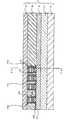
図1及び図2は、不揮発性半導体記憶装置のメモリセルアレイを構成する薄膜トランジスタを示す概略断面図である。図2は、図1に示した前記薄膜トランジスタ1の断面をチャネル/ゲート層171側から17N側方向に見たときの概略断面図である。 1 and 2 are schematic cross-sectional views showing thin film transistors that constitute a memory cell array of a nonvolatile semiconductor memory device. FIG. 2 is a schematic cross-sectional view of the
図2に示すMONOS構造は、半導体(チャネル層)14とゲート電極16との間に、第1の絶縁層15a、電荷蓄積層15b、第2の絶縁層15cの三層の積層構造となっている。この第1の絶縁層15aの材質として酸化膜(Oxide)、電荷蓄積層15bの材質として窒化膜(Nitride)、第2の絶縁層15cの材質として酸化膜(Oxide)が用いられることから、この三層構造を「ONO膜」という。なお、前記電荷蓄積層15bの材質としてポリシリコンを用いて、フローティングゲート構造としてもよい。The MONOS structure shown in FIG. 2 is a three-layered structure of a first
ONO膜の中心の電荷蓄積層(窒化膜)15bは、絶縁膜であるが、大量のトラップが存在するため、電荷を捕獲して蓄積することができる。ONO膜は、このトラップに電荷を蓄積したり、蓄積した電荷を放電したりすることにより、不揮発性半導体記憶装置のメモリセルとして利用される。The charge storage layer (nitride film) 15b at the center of the ONO film is an insulating film. However, since a large amount of traps exist, charges can be captured and stored. The ONO film is used as a memory cell of a nonvolatile semiconductor memory device by accumulating charges in this trap or discharging the accumulated charges.
さらに、本発明に係る実施例1は、半導体(チャネル層)14と、ソース/ドレイン領域121〜12Nとの間に不純物拡散制御膜1001〜100Nを設けて、前記ソース/ドレイン領域121〜12Nからチャネル層14へ不純物の拡散を制限又は制御する構造としている。この不純物拡散制御膜1001〜100Nは絶縁物である。そこで、前記MONOS構造のメモリセルとして動作させるときには、不純物拡散制御膜1001〜100Nの絶縁破壊を行い、前記ソース/ドレイン領域121〜12Nとチャネル層14との間にpn接合を形成する必要がある。Further, according to the first embodiment of the present invention, impurity
不純物拡散制御膜1001〜100Nの絶縁破壊の方法は、後述する実施例2において詳細に説明するが、ソース/ドレイン領域を少なくとも1つ選択し、0Vに調整する。この選択したソース/ドレイン領域以外のソース/ドレイン領域及びゲート電極には5〜20V程度の電圧を印加する。これにより、選択したソース/ドレイン領域上部の不純物拡散制御膜が絶縁破壊される。これを繰り返し行うことにより、全ての不純物拡散制御膜が絶縁破壊される。The method of dielectric breakdown of the impurity
このように高熱が加わる工程のために不純物拡散制御膜1001〜100Nを設けるとともに、以後高熱が加わらない工程段階において不純物拡散制御膜1001〜100Nを絶縁破壊させることによって、チャネル層の不純物濃度のばらつきを低減し薄膜トランジスタの特性(閾値)のばらつきを低減して、機能的に安定した半導体装置を提供することができる。In this way, the impurity
以下、図1及び図2に示した本発明に係る実施例1の半導体装置を構成する薄膜トランジスタの構造について詳細に説明する。Hereinafter, the structure of the thin film transistor constituting the semiconductor device according to the first embodiment of the present invention shown in FIGS. 1 and 2 will be described in detail.
層間膜11は、シリコン基板10上の所定の位置に形成されたコントロール回路、ロウデコーダ及びその他の周辺回路(図示せず)上に絶縁体を堆積させて構成したものであって、平坦化されている。この層間膜11は、膜厚200〜500nm程度のSiO2膜を形成することによりできる。The
ソース/ドレイン領域の配線(以下、「S/D領域」という。)121、122・・・12Nは、不純物を含む半導体により構成され、50〜200nm程度の膜厚で形成されることが好ましい。なお、本願発明において、不純物とは、半導体内において、キャリア(正孔又は電子)を作り出すイオンのことである。前記ソース/ドレインの材質として、非晶質シリコン、微結晶シリコン、多結晶シリコン等が好ましく、不純物としてゲルマニウム、ニッケル、リン、ホウ素、ヒ素等を挙げられる。不純物濃度は、不純物の種類によって異なるが、具体的には10E+19〜10E+21ions/cm3程度の範囲内とすることが好ましい。The wirings in the source / drain regions (hereinafter referred to as “S / D regions”) 121, 122... 12N are preferably made of a semiconductor containing impurities and are formed to a thickness of about 50 to 200 nm. In the present invention, the impurities are ions that create carriers (holes or electrons) in the semiconductor. The material of the source / drain is preferably amorphous silicon, microcrystalline silicon, polycrystalline silicon or the like, and examples of impurities include germanium, nickel, phosphorus, boron, arsenic and the like. Although the impurity concentration varies depending on the type of impurity, specifically, it is preferable to be within a range of about 10E + 19 to 10E + 21 ions / cm3 .
また、S/D領域121、122・・・12N間は、絶縁体で充填されており、これらの配線層の上面が露出する程度の高さに平坦化されている。尚、該絶縁体として、層間膜11と同様の絶縁体を用いることができる。 Further, the space between the S /
不純物拡散制御膜1001〜100Nは、S/D領域121〜12Nとチャネル層14との間に形成されている。前記不純物拡散制御膜1001〜100Nの材質としては、二酸化珪素、窒化シリコン、酸化タンタル、酸化アルミニウム等が挙げられる。また、前記不純物拡散制御膜1001〜100Nの寸法として、幅は前記S/D領域121、122・・・12Nの幅と等しくされ、膜厚は0.5〜10.0nm程度の範囲内に形成される。不純物拡散制御膜1001〜100Nの膜厚を1.0〜10.0nm程度に形成した場合、熱履歴に関わらず、ソース/ドレインに含まれる不純物がチャネル層14に拡散せず遮蔽されるので、各層の薄膜トランジスタの特性が劣化せず、微細化され高密度化された半導体装置を製造することができ、その半導体装置は機能的に安定する。また、不純物拡散制御膜1001〜100Nの膜厚を0.5〜1.0nm程度に形成した場合、熱履歴の異なる各層の薄膜トランジスタにおける拡散長を所望の範囲内に揃えることができる。 The impurity
図1及び図2に示すように、S/D領域121〜12Nに対して、チャネル層14、第1の絶縁層15a、電荷蓄積層15b、第2の絶縁層15cの三層の積層構造及びゲート電極16がいずれも上側から直角に交差するように形成されている。そして、図1に示すように、チャネル/ゲート層171〜17Nが、等間隔を開けて相互に平行になるように形成され、いずれのチャネル/ゲート層も、S/D領域121〜12Nに対して上側から直角に交差するように形成される。 As shown in FIGS. 1 and 2, for the S /
前記チャネル層14の寸法は特に限定されないが、幅厚として約200nm以下であることが好ましい。チャネル層14を構成する材質として、非晶質シリコン、微結晶シリコン、多結晶シリコン等が好ましく、不純物としてゲルマニウム、ニッケル、リン、ホウ素、ヒ素等を含有していても良い。尚、チャネル層14の不純物濃度(不純物イオンのドープ量)は、S/D領域121〜12Nに含有される不純物濃度より相対的に低いことが好ましい。 The dimension of the
チャネル層14上は、前記したとおり、第1の絶縁層15a、電荷蓄積層15b、第2の絶縁層15cから構成されている。この第1の絶縁層15aの材質として酸化膜(Oxide)、電荷蓄積層15bの材質として窒化膜(Nitride)、第2の絶縁層15cの材質として酸化膜(Oxide)が用いられる。これらの絶縁体は、スパッタ法、CVD法、リモートプラズマCVD及びLPCVD等の方法により形成される。第1の絶縁層15a、電荷蓄積層15b、第2の絶縁層15cの三層の積層構造は、2〜20nm程度の膜厚に形成される。 As described above, the
ゲート電極16は、第1の絶縁層15a、電荷蓄積層15b、第2の絶縁層15cの三層の積層構造を介してチャネル層14上に形成され、その寸法は特に限定されるものはない。尚、ゲート電極16は、膜厚が50〜200nm程度の範囲内のポリシリコン表面をクロム、チタン、銅、アルミニウム、モリブデン、タングステン、パラジウム、ニッケル、金、白金、有機半導体等から適宜選択された金属でシリサイド化することにより、形成することができる。 The
また、図1に示すように、チャネル/ゲート層171〜17Nの側壁には、絶縁体としての保護膜171a〜17Naを形成することもできる。これらの保護膜は、材料として二酸化珪素、窒化シリコン、酸化タンタル、酸化アルミニウム等の絶縁体が好適に使用され、これらの絶縁体を適宜選択して、スパッタ法、CVD法、リモートプラズマCVD及びLPCVD等の方法により、10〜30nm程度の膜厚に形成される。更に、絶縁膜からなる層間膜18及び19で、該保護膜171a〜17Naを充填し、チャネル/ゲート層171〜17Nの上端面から100〜400nm程度の膜厚で完全に充填することで、薄膜トランジスタ1が形成される。尚、前記層間膜18及び19は、層間膜11と同様の絶縁体を用いることができる。 Further, as shown in FIG. 1,
前記ソース/ドレイン領域12、チャネル層14、第1の絶縁層15a、電荷蓄積層15b、第2の絶縁層15cの三層の積層構造及びゲート電極16は、プラズマ化学的気相成長(CVD)法、低圧CVD法等の形成工程により、所定の膜厚に形成される。尚、ソース/ドレイン領域12、及びチャネル層14に不純物を注入する方法として、イオン打ち込み法、イオンドーピング法が挙げられる。また、不純物拡散制御膜は、スパッタ法、常圧CVD法、低圧CVD法、プラズマCVD法、リモートプラズマCVD法等により、絶縁膜を形成することが好ましい。 The stacked structure of the source / drain region 12, the
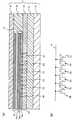
図3(a)は、不揮発性半導体記憶装置のメモリセルアレイを構成する薄膜トランジスタを示す概略断面図である。図3(b)は、図3(a)に対応する等価回路図である。FIG. 3A is a schematic cross-sectional view showing a thin film transistor constituting a memory cell array of the nonvolatile semiconductor memory device. FIG. 3B is an equivalent circuit diagram corresponding to FIG.
図3(a)に示す、ソース/ドレイン領域121〜12Nは、図3(b)に示す、薄膜トランジスタTr1〜TrNのソー/ドレイン端子121〜12Nに対応している。また、図3(a)に示す、ゲート電極16は、図3(b)に示す、ゲート端子16に対応している。薄膜トランジスタTr1〜TrNは、それぞれメモリセルとして機能する。 The source /
図3(a)に示す不揮発性半導体記憶装置は、第1の絶縁層15a、電荷蓄積層15b、第2の絶縁層15cの三層の積層構造を有する。この電荷蓄積層15bをフローティングゲートとして電荷を蓄積する不揮発性の半導体装置である。The nonvolatile semiconductor memory device shown in FIG. 3A has a three-layer structure of a first insulating
次に、メモリセルの書き込み、消去、読み出しの各動作について、図3(a)及び図4(a)〜(c)を用いて説明する。図4(a)は、薄膜トランジスタTr1〜TrNのうち、薄膜トランジスタTr3にデータを書き込むときの動作電圧を示した図である。薄膜トランジスタTr1〜TrNのゲート電極16は、全て共通で、約17V程度くらいまでの高電圧を印加する。データを書き込む対象である薄膜トランジスタTr3のS/D領域(ソース/ドレイン電極)123、124は、0Vとする。それ以外のS/D領域(ソース/ドレイン電極)121、122、125、12Nは、開放(OPEN)とする。このようにすると、薄膜トランジスタTr3のドレイン/ソース123と124との間のチャネル層14と、とゲート電極16との間にトンネル電流が流れる。トンネル効果により電子は、第1の絶縁層15aを貫通して、電荷蓄積層15bに注入される。この電子が電荷蓄積層15bに注入されることにより情報の書き込みがなされる。なお、図4(a)では、書き込み対象がTr3のみであったが、書き込む対象となる薄膜トランジスタのS/D領域(ソース/ドレイン電極)を0Vとすることで、データを書き込むことができる。 Next, each operation of writing, erasing, and reading of the memory cell will be described with reference to FIGS. 3A and 4A to 4C. FIG. 4A shows an operating voltage when data is written to the thin film transistor Tr3 among the thin film transistors Tr1 to TrN. The
図4(b)は、薄膜トランジスタTr1〜TrNのうち、薄膜トランジスタTr3のデータを消去するときの動作電圧を示した図である。薄膜トランジスタTr1〜TrNのゲート電極16は、全て共通で、約−4V程度の負電圧を印加する。データの消去を行う対象である薄膜トランジスタTr3のS/D領域(ソース/ドレイン電極)123、124は、3V程度の電圧を印加する。それ以外のS/D領域(ソース/ドレイン電極)121、122、125、12Nは、0Vとする。このようにすると、薄膜トランジスタTr3のドレイン/ソース123と124との間のチャネル層14と、とゲート電極16との間に、上記した書き込み動作時とは逆のトンネル電流が流れる。電荷蓄積層15bに注入されていた電子は、第1の絶縁層15aを貫通して、チャネル層14に移動する。電荷蓄積層15bに注入されていた電子が、第1の絶縁層15aを貫通して、チャネル層14に移動することにより情報の消去が行われる。なお、図4(b)では、データの消去対象がTr3のみであったが、消去対象となる薄膜トランジスタのS/D領域(ソース/ドレイン電極)を3V程度とすることで、データを消去することができる。FIG. 4B is a diagram showing an operating voltage when erasing data of the thin film transistor Tr3 among the thin film transistors Tr1 to TrN. The
図4(c)は、薄膜トランジスタTr1〜TrNのうち、薄膜トランジスタTr3のデータを読み出すときの動作電圧を示した図である。薄膜トランジスタTr1〜TrNのゲート電極16は、全て共通で、約3V程度の電圧を印加する。データの読み出しを行う対象である薄膜トランジスタTr3のS/D領域(ソース/ドレイン電極)のソース側124は、0Vとし、ドレイン側123は、1.5V程度の電圧を印加する。それ以外のS/D領域(ソース/ドレイン電極)125、12Nは、0Vまたは開放(OPEN)とし、121、122は、3V程度または開放(OPEN)とする。このようにすると、Tr3の電荷蓄積層15bに電子が蓄積されているときには、Tr3のドレインとソースとの間には電流はほとんど流れない。これに対して、Tr3の電荷蓄積層15bに電子が蓄積されていないときには、Tr3のドレインとソースとの間には電流が流れる。すなわち、前記電荷蓄積層15bに注入された電子は、前記薄膜トランジスタのチャネル領域の導通を制御し、その結果前記薄膜トランジスタの導通を検出することにより、前記電荷蓄積層15bに保持されている二値情報の内容が検出される。FIG. 4C is a diagram showing an operating voltage when reading data from the thin film transistor Tr3 among the thin film transistors Tr1 to TrN. The
以上のように構成された薄膜トランジスタ1は、MONOS構造のメモリセルとして使用することが可能となり、不揮発性半導体記憶装置として機能する。但し、本発明はこれに限定して解釈されるものではなく、本実施例1の半導体装置の応用範囲は、液晶ディスプレイ装置、メモリ等多岐にわたる。The
以下、本発明の実施例1の半導体装置の製造方法について、工程別に素子の断面を示した図5〜図10を用いて説明する。
(1)S/D領域121〜12Nの形成工程
まず、図5に示すように、CMOSプロセスを用いて、シリコン基板10上にコントロール回路、ロウデコーダ及びその他の周辺回路を所望の位置に形成し(図示せず)、これらの回路上に絶縁膜よりなる層間膜11を堆積させることにより充填し、前記層間膜11を平坦化した。その後、前記層間膜11上に、所望の位置に、n型不純物をドープしたポリシリコン(又はアモルファスシリコン)をCVD法や低圧化学的気相成長(LPCVD)等の方法により堆積し、前記堆積したポリシリコンを配線状にエッチングすることにより、所望の数の並列したN本のS/D領域121〜12Nが等間隔を開けて相互に平行になるように形成した。Hereinafter, the manufacturing method of the semiconductor device of Example 1 of this invention is demonstrated using FIGS. 5-10 which showed the cross section of the element according to the process.
(1) Step of forming S /
次に、図6に示すように、層間膜13を層間膜11上に堆積させることにより、S/D領域121〜12N間を絶縁体で充填する。絶縁体による充填後、或いは絶縁体で充填しつつ、S/D領域121〜12Nの上面が露出する程度の高さに平坦化する。 Next, as shown in FIG. 6, the
(2)不純物拡散制御膜の形成工程
次に、図7に示すように、S/D領域121〜12Nの各上面に、S/D領域121〜12Nの各上面を熱酸化することにより、不純物拡散制御膜1001〜100Nとなる膜厚2nm程度のSiO2膜を形成した。(2) Impurity Diffusion Control Film Forming Step Next, as shown in FIG. 7, the upper surfaces of the S /
(3)チャネル層及びゲート電極(チャネル/ゲート層)の形成工程
次に、図8に示すように、p型不純物を含んだポリシリコン(又はアモルファスシリコン)をCVD法やLPCVD等の方法により、膜厚50nm程度のチャネル層14を形成する。このとき、前記S/D領域121〜12Nとチャネル層14の間には、不純物拡散制御膜としてのSiO2膜が形成されている。このため、S/D領域に含まれるn型不純物が、この後に熱工程等の半導体装置製造工程において加えられる熱によって、p型不純物を含んだチャネル層14内に拡散することが遮断乃至制限される。(3) Step of forming channel layer and gate electrode (channel / gate layer) Next, as shown in FIG. 8, polysilicon (or amorphous silicon) containing p-type impurities is formed by a method such as CVD or LPCVD. A
次に、図8に示すように、p型不純物を含んだポリシリコン(又はアモルファスシリコン)をCVD法により堆積した後、前記ポリシリコン表面を熱酸化することにより、膜厚2nm程度のSiO2膜15aを形成した。更に、前記成膜方法と同様の方法により、膜厚5nm程度の窒化シリコン膜15b及び膜厚8nm程度のSiO2膜15cを形成した。Next, as shown in FIG. 8, after depositing polysilicon (or amorphous silicon) containing a p-type impurity by a CVD method, the polysilicon surface is thermally oxidized to form an SiO2 film having a thickness of about2 nm. 15a was formed. Further, a
その後、図9に示すように、第1の絶縁層15a、電荷蓄積層15b、第2の絶縁層15cの三層の積層構造上に、CVD法やLPCVD等の方法により、50〜200nm程度のポリシリコン膜16aが形成し、該ポリシリコン膜16a表面をチタンサリサイド化してチタン/窒化チタン膜16bを形成し、ゲート電極16を形成した。 After that, as shown in FIG. 9, on the three-layered structure of the first insulating
次に、図10に示すように、S/D領域121に対して、チャネル層141〜14N、ゲート絶縁膜151〜15N及びゲート電極161〜16Nがいずれも上側から直角に交差するように、チャネル層141〜14N、ゲート絶縁膜151〜15N及びゲート電極161〜16Nを一括でエッチングした。これにより、所望の数の並列したチャネル/ゲート層171〜17Nが、図10に示すように、等間隔を開けて相互に平行になるように形成され、いずれのチャネル/ゲート層も、S/D領域121に対して上側から直角に交差するように形成される。 Next, as shown in FIG. 10, the channel layers 141 to 14N, the
次に、図1に示すように、チャネル/ゲート層171〜17Nの側壁に、絶縁体としての保護膜171a〜17Naを形成した。この実施例では、チャネル/ゲート層171〜17Nの側壁、すなわち、チャネル層141〜14N、ゲート絶縁膜151〜15N及びゲート電極161〜16Nの側壁を熱酸化することにより、保護膜171a〜17Naを形成した。その後、絶縁膜からなる層間膜18及び19で、該保護膜171a〜17Naを充填し、チャネル/ゲート層171〜17Nの上端面から100〜400nm程度の膜厚で完全に充填することで、1層目の薄膜トランジスタ1が形成される。尚、前記層間膜18及び19は、層間膜11、13と同様の絶縁体を材料として用い、同様の方法にて成膜することができる。 Next, as shown in FIG. 1,
実施例1の半導体装置は、以上のように製造された1層の薄膜トランジスタ1により構成される。 The semiconductor device of Example 1 is constituted by a single-layer
〔実施例2〕
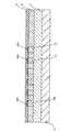
実施例2の半導体装置は、図11及び図12に示されるように、実施例1を構成する薄膜トランジスタ1が積層化されて高密度化されて構成される。2層目以上にある薄膜トランジスタは、実施例1の半導体装置を製造する工程を繰り返す。薄膜トランジスタ1上に2層目の薄膜トランジスタ2、3層目の薄膜トランジスタ3を順次形成し、図11及び図12に示すように所望の積層数の三次元積層メモリを形成することができる。尚、図12は、実施例1の薄膜トランジスタをチャネル/ゲート層171側からソース/ドレイン領域121〜12Nに対して平行な方向に見た概略断面図である。[Example 2]
As shown in FIGS. 11 and 12, the semiconductor device according to the second embodiment is configured by stacking and densifying the
図11及び図12に示す構造の実施例2の半導体装置は、第1の実施例と同様に、薄膜トランジスタを、MONOS(Metal−Oxide−Nitride−Oxide−Semiconductor)構造にして、不揮発性半導体記憶装置のメモリセルとして利用する例を示している。The semiconductor device of Example 2 having the structure shown in FIG. 11 and FIG. 12 has a MONOS (Metal-Oxide-Nitride-Oxide-Semiconductor) structure as a non-volatile semiconductor memory device, as in the first example. An example of use as a memory cell is shown.
不純物拡散制御膜が介在したままの状態であると、薄膜トランジスタ1、2及び3を構成するそれぞれのソース/ドレイン領域とチャネル層との間は、電気的に絶縁状態であるため、薄膜トランジスタとして動作しない。そこで、最後の工程において、不純物拡散制御膜の絶縁破壊を行う。If the impurity diffusion control film remains in the state, the source / drain regions and the channel layer constituting the
前記不純物拡散制御膜は、次の工程により絶縁破壊される。まず、各層の薄膜トランジスタにおいて、ソース/ドレイン領域を少なくとも1つ選択する。選択されたソース/ドレイン領域と、他のソース/ドレイン領域及びゲート電極との間に高電圧を印加する。これにより、選択されたソース/ドレイン領域上の不純物拡散制御膜が絶縁破壊される。 The impurity diffusion control film is broken down by the following process. First, at least one source / drain region is selected in each thin film transistor. A high voltage is applied between the selected source / drain region and the other source / drain regions and the gate electrode. Thereby, the impurity diffusion control film on the selected source / drain region is broken down.
図13に一例を示す。図13に示す電極配線A1乃至A3から電極配線a1乃至a3を介して、各層の薄膜トランジスタのゲート電極に例えば7V程度を印加する。絶縁破壊の対象となる不純物拡散制御膜がその上部に形成されたソース/ドレイン領域の電位は、0Vに調整する。それ以外のソース/ドレイン領域の電位はいずれも7V程度になるようにバイアスする。なお、このソース/ドレイン領域には、図13に示した電極配線A1乃至A3から電極配線a1乃至a3を介して7V程度を印加する。これによって、0Vに調整したソース/ドレイン領域の上部の不純物拡散制御膜は、絶縁破壊される。An example is shown in FIG. For example, about 7 V is applied to the gate electrode of the thin film transistor in each layer from the electrode wirings A1 to A3 shown in FIG. 13 via the electrode wirings a1 to a3. The potential of the source / drain region in which the impurity diffusion control film to be subjected to dielectric breakdown is formed is adjusted to 0V. The other source / drain regions are biased so that the potential is about 7V. Note that about 7 V is applied to the source / drain regions from the electrode wirings A1 to A3 shown in FIG. 13 via the electrode wirings a1 to a3. As a result, the impurity diffusion control film above the source / drain region adjusted to 0 V is broken down.
ソース/ドレイン領域を順次選択して上記絶縁破壊工程を行うことにより、全ての層の薄膜トランジスタのソース/ドレイン領域とチャネル層との間に介在する不純物拡散制御膜を静電破壊しpn接合を形成する。前記絶縁破壊工程により、図11及び図12に示す構造の実施例2の半導体装置は、薄膜トランジスタ動作及びメモリ動作を正常に行うことができる。 By sequentially selecting the source / drain regions and performing the dielectric breakdown process, the impurity diffusion control film interposed between the source / drain regions of all the thin film transistors and the channel layer is electrostatically broken to form a pn junction. To do. By the dielectric breakdown process, the semiconductor device of the second embodiment having the structure shown in FIGS. 11 and 12 can normally perform the thin film transistor operation and the memory operation.
[実施例3]
実施例3は、実施例1と異なり、S/D領域121〜12N及び層間膜13上にSiO2膜を堆積(デポ)させる方法により形成する形態である。すなわち、実施例1は、S/D領域121〜12Nの各上面を熱酸化することにより、膜厚2nm程度のSiO2膜の不純物拡散制御膜をそれぞれ形成したが、実施例3は、SiO2膜の不純物拡散制御膜を堆積(デポ)させる方法により形成する方法を採る。[Example 3]
The third embodiment is different from the first embodiment in that the SiO2 film is deposited (deposited) on the S /
図14に示すように、層間膜11上にS/D領域121〜12Nを形成し、層間膜13を層間膜11上に堆積させて、S/D領域121〜12N間を絶縁体で充填した後、SiO2膜の不純物拡散制御膜1000を、気相成長法を用いて堆積させる。従って、不純物拡散制御膜1000は、S/D領域121〜12Nの各上面だけでなく、S/D領域121〜12N及び層間膜13上全面に形成される。As shown in FIG. 14, S /
不純物拡散制御膜1000を、堆積させた後の工程は、図15及び図16に示すように、実施例1と同じである。 The process after depositing the impurity
[実施例4]
実施例4の半導体装置は、図18に示されるように、実施例2を構成する薄膜トランジスタ1が積層化されて高密度化されて構成される。2層目以上にある薄膜トランジスタは、実施例2の半導体装置を製造する工程を繰り返す。薄膜トランジスタ1上に2層目の薄膜トランジスタ2、3層目の薄膜トランジスタ3を順次形成し、図18に示すように所望の積層数の三次元積層メモリを形成することができる。[Example 4]
As shown in FIG. 18, the semiconductor device according to the fourth embodiment is configured by stacking and densifying the
また、不純物拡散制御膜を、絶縁破壊する工程も図19に示すように実施例2と同じである。図19に示す電極配線A1乃至A3から電極配線a1乃至a3を介して、各層の薄膜トランジスタのゲート電極に例えば7V程度を印加する。絶縁破壊の対象となる不純物拡散制御膜がその上部に形成されたソース/ドレイン領域の電位は、0Vに調整する。それ以外のソース/ドレイン領域の電位はいずれも7V程度になるようにバイアスする。Further, the process of dielectric breakdown of the impurity diffusion control film is the same as that of the second embodiment as shown in FIG. For example, about 7 V is applied to the gate electrode of the thin film transistor of each layer from the electrode wirings A1 to A3 shown in FIG. 19 via the electrode wirings a1 to a3. The potential of the source / drain region in which the impurity diffusion control film to be subjected to dielectric breakdown is formed is adjusted to 0V. The other source / drain regions are biased so that the potential is about 7V.
ソース/ドレイン領域を順次選択して上記絶縁破壊工程を行うことにより、全ての層の薄膜トランジスタのソース/ドレイン領域とチャネル層との間に介在する不純物拡散制御膜を静電破壊しpn接合を形成する。前記絶縁破壊工程により、図18に示す実施例3の半導体装置は、薄膜トランジスタ動作及びメモリ動作を正常に行うことができる。 By sequentially selecting the source / drain regions and performing the dielectric breakdown process, the impurity diffusion control film interposed between the source / drain regions of all the thin film transistors and the channel layer is electrostatically broken to form a pn junction. To do. By the dielectric breakdown process, the semiconductor device of Example 3 shown in FIG. 18 can normally perform the thin film transistor operation and the memory operation.
[実施例5]
実施例1と同様の要領にて、ソース/ドレイン領域を形成し配線状に加工し層間膜を充填し平坦化した後、前記ソース/ドレイン領域の上面を窒化して膜厚が0.5nm〜2.0nm程度の範囲内の窒化膜(SiN)で不純物拡散制御膜を形成する。チャネル層の不純物は、ソース/ドレイン領域の不純物が拡散されるようにして注入される。チャネル層に拡散される不純物の量は、加えられる熱に応じて変わる。加えられる熱履歴が多いほど、チャネル層に拡散される不純物の量は多い。そこで、不純物拡散制御膜は、チャネル層に拡散される不純物が一定の範囲に収まるように、窒化膜で形成され一定の膜厚になるように形成される。と同時に他方で、不純物拡散制御膜は、半導体製造工程完了後にソース/ドレイン領域とチャネル層との間にオーミックコンタクトが形成できるようにし、電流が流れるようにする。不純物拡散制御膜の膜厚は、加えられる熱に応じて変える必要があるが、概ね0.5nm以上2.0nm以下の範囲で形成すれば、チャネル層に拡散される不純物の量とオーミックコンタクトの形成ができる。なお、実施例3と同様の要領にて、S/D領域121〜12N及び層間膜13上に窒化膜(SiN)を堆積(デポ)させる方法により形成してもよい。次いで、実施例1又は実施例3と同様の要領にて、チャネル/ゲート層を形成する。[Example 5]
In the same manner as in Example 1, source / drain regions are formed and processed into a wiring shape, filled with an interlayer film and planarized, and then the upper surface of the source / drain regions is nitrided to have a thickness of 0.5 nm to An impurity diffusion control film is formed of a nitride film (SiN) within a range of about 2.0 nm. The impurities in the channel layer are implanted so that the impurities in the source / drain regions are diffused. The amount of impurities diffused into the channel layer varies depending on the applied heat. The more heat history that is applied, the more impurities are diffused into the channel layer. Therefore, the impurity diffusion control film is formed of a nitride film and has a constant film thickness so that impurities diffused in the channel layer are within a certain range. At the same time, on the other hand, the impurity diffusion control film allows an ohmic contact to be formed between the source / drain region and the channel layer after completion of the semiconductor manufacturing process, and allows current to flow. The film thickness of the impurity diffusion control film needs to be changed according to the applied heat, but if formed within a range of approximately 0.5 nm to 2.0 nm, the amount of impurities diffused into the channel layer and the ohmic contact Can be formed. In the same manner as in the third embodiment, a nitride film (SiN) may be deposited (deposited) on the S /
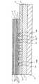
図20は、本発明に係る実施例5の半導体装置を示す概略断面図である。図21は、図20に示した半導体装置の断面をチャネル/ゲート層171側から17N側方向に見たときの概略断面図である。実施例5の半導体装置が実施例1乃至実施例4と異なる点は、ソース/ドレイン領域とチャネル層との間に形成される不純物拡散制御膜1001の膜厚が一定の範囲で薄く形成されており、かつ、不純物拡散制御膜の材質として窒化膜が用いられる点である。実施例5の半導体装置の場合、不純物拡散制御膜は、ソース/ドレイン領域からチャネル層へ拡散する不純物を遮蔽する働きまではせずに、不純物の拡散量を一定に制御するように、その膜厚が薄く形成され、材質として窒化膜が用いられる。これによって、ソース/ドレイン領域とチャネル層との間にpn接合が形成されていなくても、半導体製造工程において熱が加わる段階においては、ソース/ドレイン領域からチャネル層へのn型不純物の拡散量が所望の温度において所望の拡散長になるように制御することができ、半導体製造工程が完了するときには、ソース/ドレイン領域とチャネル層との間にオーミックコンタクトを形成することができ、かつ、電流が流れるようにすることができる。また、前記した実施例1乃至実施例4と異なり、不純物拡散制御膜1001を絶縁破壊する工程を省くことができる。FIG. 20 is a schematic cross-sectional view showing a semiconductor device according to Example 5 of the present invention. FIG. 21 is a schematic cross-sectional view of the semiconductor device shown in FIG. 20 as viewed from the channel /
[実施例6]
実施例1又は実施例3と同様の要領にて、ソース/ドレイン領域を形成し配線状に加工し層間膜を充填し平坦化した後、前記ソース/ドレイン領域の上面又は前記ソース/ドレイン領域及び層間膜の上面全面に膜厚t1の不純物拡散制御膜を形成する。次いで、実施例1と同様の要領にて、チャネル/ゲート層を形成し、最下層の薄膜トランジスタを製造する。[Example 6]
In the same manner as in Example 1 or Example 3, source / drain regions are formed and processed into wiring, filled with an interlayer film and planarized, and then the upper surface of the source / drain regions or the source / drain regions and forming an impurity diffusion control film having a thickness t1 on the entire upper surface of the interlayer film. Next, in the same manner as in Example 1, a channel / gate layer is formed, and the lowermost thin film transistor is manufactured.
次に、実施例2又は実施例4と同様の要領にて、最下層の薄膜トランジスタの上層に、複数の薄膜トランジスタを形成するが、第N層の薄膜トランジスタ(Nは整数)の不純物拡散制御膜の膜厚tNは、下層のトランジスタの不純物拡散制御膜の膜厚よりも相対的に薄く形成され、例えば、0.5≦tN<・・・<t2<t1≦2.0nm程度の範囲内で窒化シリコンを形成する。それ以外は、実施例1又は実施例3と同様にして不純物拡散制御膜を形成する。Next, in the same manner as in Example 2 or Example 4, a plurality of thin film transistors are formed in the upper layer of the lowermost thin film transistor, but the impurity diffusion control film of the Nth thin film transistor (N is an integer) the thicknesst N, rather than the film thickness of the impurity diffusion control film of the lower layer of the transistor is relatively thin, forexample, 0.5 ≦ t N <··· < t 2 <
図22は、本発明に係る実施例6の複数の薄膜トランジスタを形成した半導体装置を示す概略断面図である。図23は、実施例6の薄膜トランジスタをチャネル/ゲート層171側からソース/ドレイン領域121〜12Nに対して平行な方向に見た概略断面図である。図22及び図23に示した本発明に係る実施例6の複数の薄膜トランジスタを形成した半導体装置は、3層構造としている。最下層の薄膜トランジスタの不純物拡散制御膜1001の膜厚t1から順に第2層目の薄膜トランジスタの不純物拡散制御膜2001の膜厚t2、最上層の薄膜トランジスタの不純物拡散制御膜3001の膜厚t3と上層になるに従い、膜厚が薄く形成される。複数の薄膜トランジスタを積層化して高密度化する場合、上層側と下層側の薄膜トランジスタでは、それぞれサーマルバジェットが異なる。すなわち、下層の薄膜トランジスタである程、その上層の薄膜トランジスタの製造工程における熱処理の影響を受けることになるが、上層の薄膜トランジスタである程、その更に上層に形成される薄膜トランジスタの製造工程における熱処理の影響が少なくなる。
従って、薄膜トランジスタを1層目、2層目、3層目・・・と積層して半導体装置を構成する場合、各層に形成される不純物拡散制御膜を順に薄くしていく。これにより、最終的に半導体製造工程が完了したときに、各階層における不純物の拡散長を同程度に制御することが可能で、各層の薄膜トランジスタ特性のバラツキを低減することができる。FIG. 22 is a schematic sectional view showing a semiconductor device in which a plurality of thin film transistors of Example 6 according to the present invention are formed. FIG. 23 is a schematic cross-sectional view of the thin film transistor of Example 6 as viewed from the channel /
Therefore, when a semiconductor device is formed by stacking thin film transistors with the first layer, the second layer, the third layer,..., The impurity diffusion control film formed in each layer is made thinner in order. Thereby, when the semiconductor manufacturing process is finally completed, the impurity diffusion length in each layer can be controlled to the same level, and variations in thin film transistor characteristics in each layer can be reduced.
[実施例7]
実施例1又は実施例3と同様の要領にて、ソース/ドレイン領域を形成し配線状に加工し層間膜を充填し平坦化した後、前記ソース/ドレイン領域の上面又は前記ソース/ドレイン領域及び層間膜の上面全面に不純物拡散制御膜を形成する。次いで、前記S/D領域に含まれる不純物と同じタイプの不純物を含んだポリシリコンを用いてチャネル層を構成する以外、実施例1又は実施例3と同様の要領にてチャネル/ゲート層を形成しする。この製造工程により製造された薄膜トランジスタは、通常状態においてはオンであり、ゲート電極をマイナス側にするとチャネル層が完全に空乏化してオフになる、デプレッションタイプのノーマリ・オン型のものである。[Example 7]
In the same manner as in Example 1 or Example 3, source / drain regions are formed and processed into wiring, filled with an interlayer film and planarized, and then the upper surface of the source / drain regions or the source / drain regions and An impurity diffusion control film is formed on the entire upper surface of the interlayer film. Next, a channel / gate layer is formed in the same manner as in Example 1 or Example 3 except that the channel layer is formed using polysilicon containing impurities of the same type as the impurity contained in the S / D region. To do. The thin film transistor manufactured by this manufacturing process is a depletion-type normally-on type in which the thin film transistor is on in a normal state and the channel layer is completely depleted and turned off when the gate electrode is set to the negative side.
本実施例においても、チャネル層のn型不純物の濃度を空乏化させ得る閾値を変化させるため、ソース/ドレイン領域と、チャネル層との間には、不純物拡散制御膜を形成し、n不純物が拡散しないようにする必要がある。 Also in this embodiment, an impurity diffusion control film is formed between the source / drain regions and the channel layer in order to change the threshold value at which the concentration of the n-type impurity in the channel layer can be depleted. It is necessary not to spread.
本実施例においても、プロセス完了後、ソース/ドレイン領域とチャネル層との間に高電界を掛けて絶縁破壊することで、pn接合を形成することができる。前記製造工程により製造された実施例7の半導体装置は、実施例1又は実施例3の半導体装置がデプレッションタイプのノーマリ・オン型の薄膜トランジスタで構成されたものである。 Also in this embodiment, after the process is completed, a pn junction can be formed by applying a high electric field between the source / drain regions and the channel layer to cause a dielectric breakdown. The semiconductor device of Example 7 manufactured by the manufacturing process is a semiconductor device of Example 1 or Example 3 configured by a depletion type normally-on type thin film transistor.
[実施例8]
実施例1又は実施例3と同様の要領にて、ソース/ドレイン領域を形成し配線状に加工し層間膜を充填し平坦化した後、前記ソース/ドレイン領域の上面又は前記ソース/ドレイン領域及び層間膜の上面全面に不純物拡散制御膜を形成する。次いで、前記S/D領域に含まれる不純物と同じタイプの不純物を含んだポリシリコンを用いてチャネル層を構成する以外、実施例2又は実施例4と同様の要領にてチャネル/ゲート層を形成し、複数の層の薄膜トランジスタを順次製造する。この製造工程により製造された薄膜トランジスタは、通常状態においてはオンであり、ゲート電極をマイナス側にするとチャネル層が完全に空乏化してオフになる、デプレッションタイプのノーマリ・オン型のものである。[Example 8]
In the same manner as in Example 1 or Example 3, source / drain regions are formed and processed into wiring, filled with an interlayer film and planarized, and then the upper surface of the source / drain regions or the source / drain regions and An impurity diffusion control film is formed on the entire upper surface of the interlayer film. Next, a channel / gate layer is formed in the same manner as in Example 2 or Example 4 except that the channel layer is formed using polysilicon containing impurities of the same type as the impurities contained in the S / D region. Then, thin film transistors having a plurality of layers are sequentially manufactured. The thin film transistor manufactured by this manufacturing process is a depletion-type normally-on type in which the thin film transistor is on in a normal state and the channel layer is completely depleted and turned off when the gate electrode is set to the negative side.
そして、前記製造工程により製造された実施例8の半導体装置は、実施例2又は実施例4の半導体装置がデプレッションタイプのノーマリ・オン型の薄膜トランジスタで構成されたものである。 The semiconductor device of Example 8 manufactured by the manufacturing process is a semiconductor device of Example 2 or Example 4 configured by a depletion type normally-on type thin film transistor.
[実施例9]
実施例5と同様の要領にて、ソース/ドレイン領域を形成し配線状に加工し層間膜を充填し平坦化した後、前記ソース/ドレイン領域の上面に窒化した不純物拡散制御膜を形成する。次いで、前記S/D領域に含まれる不純物と同じタイプの不純物を含んだポリシリコンを用いてチャネル層を構成する以外、実施例5と同様の要領にてチャネル/ゲート層を形成し、複数の層の薄膜トランジスタを順次製造する。この製造工程により製造された薄膜トランジスタは、通常状態においてはオンであり、ゲート電極をマイナス側にするとチャネル層が完全に空乏化してオフになる、デプレッションタイプのノーマリ・オン型のものである。[Example 9]
In the same manner as in the fifth embodiment, a source / drain region is formed and processed into a wiring shape, filled with an interlayer film and planarized, and then a nitrided impurity diffusion control film is formed on the upper surface of the source / drain region. Next, a channel / gate layer is formed in the same manner as in Example 5 except that the channel layer is formed using polysilicon containing the same type of impurity as the impurity contained in the S / D region. Layered thin film transistors are sequentially manufactured. The thin film transistor manufactured by this manufacturing process is a depletion-type normally-on type in which the thin film transistor is on in a normal state and the channel layer is completely depleted and turned off when the gate electrode is set to the negative side.
そして、前記製造工程により製造された実施例9の半導体装置は、実施例5の半導体装置がデプレッションタイプのノーマリ・オン型の薄膜トラン2ジスタで構成されたものである。 The semiconductor device according to the ninth embodiment manufactured by the manufacturing process is a semiconductor device according to the fifth embodiment configured by a depletion type normally-on type thin film transistor 2 transistor.
以上、前記実施例1乃至9により、本発明の半導体装置及びその製造方法について説明したが、本発明の半導体装置及びその製造方法は、実施例1乃至9に特に限定されるものではなく、各種の変更が可能である。 As described above, the semiconductor device and the manufacturing method thereof according to the first to ninth embodiments have been described. However, the semiconductor device and the manufacturing method thereof according to the present invention are not particularly limited to the first to ninth embodiments. Can be changed.
本発明の第1の態様に係る半導体装置は、絶縁体層を介して半導体基板上に形成された、不純物を含むソース/ドレイン領域と、前記ソース/ドレイン領域間を充填する絶縁体と、前記ソース/ドレイン領域上に形成された不純物拡散制御膜層と、前記不純物拡散制御膜上に、前記ソース/ドレイン領域の延びる方向に対して直角に交差するように形成されたチャネル層と、前記チャネル層上に形成された、ゲート絶縁膜と、前記ゲート絶縁膜上に形成されたゲート電極と、前記チャネル層、ゲート絶縁膜及びゲート電極を充填するように形成された絶縁体からなる層間膜とを具備し、前記ソース/ドレイン領域と前記チャンネル層との間の前記不純物拡散制御膜が破壊され、電気的に接続される構成としている。 According to a first aspect of the present invention, there is provided a semiconductor device including a source / drain region containing impurities, an insulator filling a space between the source / drain regions, and an insulator formed on a semiconductor substrate via an insulator layer. An impurity diffusion control film layer formed on the source / drain region; a channel layer formed on the impurity diffusion control film so as to intersect at right angles to a direction in which the source / drain region extends; and the channel A gate insulating film formed on the layer; a gate electrode formed on the gate insulating film; an interlayer film made of an insulator formed to fill the channel layer, the gate insulating film, and the gate electrode; And the impurity diffusion control film between the source / drain regions and the channel layer is broken and electrically connected.
本発明の第1の態様によれば、ソース/ドレイン領域とチャネル層との間に不純物拡散制御膜が形成されることにより、前記ソース/ドレイン領域からチャネル層への不純物の拡散を制限又は制御することが可能となり、薄膜トランジスタの特性(閾値)のばらつきを低減し、機能的に安定した半導体装置を提供することができる。According to the first aspect of the present invention, the impurity diffusion control film is formed between the source / drain region and the channel layer, thereby limiting or controlling the diffusion of impurities from the source / drain region to the channel layer. Thus, variation in characteristics (threshold values) of thin film transistors can be reduced, and a functionally stable semiconductor device can be provided.
本発明の第2の態様に係る半導体装置は、前記チャネル層上に形成された、前記ゲート絶縁膜を、第1の絶縁層と電荷蓄積層と第2の絶縁層の三層を含む積層構造としている。 A semiconductor device according to a second aspect of the present invention is a stacked structure including the three layers of a first insulating layer, a charge storage layer, and a second insulating layer, the gate insulating film formed on the channel layer. It is said.
本発明の第2の態様によれば、前記チャネル層上に形成された、第1の絶縁層、電荷蓄積層及び第2の絶縁層の三層を含む積層構造を設け、MONOS構造としているので、薄膜トランジスタを不揮発性メモリセルとして使用する。前記したように、ソース/ドレイン領域とチャネル層との間に不純物拡散制御膜が形成されることにより、前記ソース/ドレイン領域からチャネル層への不純物の拡散を制限又は制御することが可能となり、薄膜トランジスタの特性(閾値)のばらつきを低減したメモリセルを有する不揮発性半導体記憶装置を提供することができる。According to the second aspect of the present invention, the laminated structure including the three layers of the first insulating layer, the charge storage layer, and the second insulating layer formed on the channel layer is provided, and the MONOS structure is formed. The thin film transistor is used as a nonvolatile memory cell. As described above, by forming the impurity diffusion control film between the source / drain region and the channel layer, it becomes possible to limit or control the diffusion of impurities from the source / drain region to the channel layer, A nonvolatile semiconductor memory device having memory cells in which variation in characteristics (threshold values) of thin film transistors is reduced can be provided.
また、本発明の第3の態様に係る半導体装置は、前記薄膜トランジスタが、複数積層され、上層の前記不純物拡散制御膜の膜厚が下層の前記不純物拡散制御膜の膜厚以下の膜厚になるように形成された構成を採る。In the semiconductor device according to the third aspect of the present invention, a plurality of the thin film transistors are stacked, and the film thickness of the upper impurity diffusion control film is equal to or smaller than the film thickness of the lower impurity diffusion control film. The structure formed in this way is adopted.
本発明の第3の態様によれば、下層側の薄膜トランジスタの不純物拡散制御膜の膜厚を厚く形成し、上層側の薄膜トランジスタの不純物拡散制御膜を下層側の膜厚に対して相対的に薄く形成することで、熱履歴の異なる各層の薄膜トランジスタにおける拡散長を、熱履歴に応じて所望の範囲内に揃えることができる。そのため、半導体装置の製造プロセスが完了するときには、各層の薄膜トランジスタに加えられる熱履歴が異なった場合であっても、各層の薄膜トランジスタの特性(閾値)のばらつきを低減し、機能的に安定した半導体装置を提供することができる。According to the third aspect of the present invention, the film thickness of the impurity diffusion control film of the lower layer thin film transistor is formed thick, and the impurity diffusion control film of the upper layer side thin film transistor is relatively thin relative to the film thickness of the lower layer side. By forming, the diffusion length in the thin film transistor of each layer having different thermal histories can be aligned within a desired range according to the thermal histories. Therefore, when the manufacturing process of the semiconductor device is completed, even if the thermal history applied to the thin film transistor of each layer is different, variation in characteristics (thresholds) of the thin film transistor of each layer is reduced, and the functionally stable semiconductor device Can be provided.
また、本発明の第4の態様に係る半導体装置の製造方法は、ソース/ドレイン領域を相互に平行になるように並列配置して、前記ソース/ドレイン領域間を充填する絶縁体を形成する工程と、前記ソース/ドレイン領域の上面に、不純物拡散制御膜を形成する工程と、前記ソース/ドレイン領域に対して直角に交差するように前記薄膜トランジスタのチャネル層を形成する工程と、前記チャネル層上にゲート絶縁膜を形成し、前記ゲート絶縁膜上に、前記薄膜トランジスタのゲート電極を形成する工程と、前記ソース/ドレイン領域と前記ゲート電極とにそれぞれ所定の電圧を印加することにより、前記不純物拡散制御膜を絶縁破壊して、ソース/ドレイン領域からチャネル層にpn接合を形成する工程からなる構成を採る。 Further, in the method of manufacturing a semiconductor device according to the fourth aspect of the present invention, the source / drain regions are arranged in parallel so as to be parallel to each other, and the insulator filling the space between the source / drain regions is formed. Forming an impurity diffusion control film on the upper surface of the source / drain region, forming a channel layer of the thin film transistor so as to intersect at right angles to the source / drain region, and on the channel layer Forming a gate insulating film on the gate insulating film, forming a gate electrode of the thin film transistor on the gate insulating film, and applying a predetermined voltage to the source / drain region and the gate electrode, respectively, A structure comprising a step of forming a pn junction from the source / drain region to the channel layer by dielectric breakdown of the control film is adopted.
本発明の第4の態様によれば、熱履歴が加わる工程では、不純物拡散制御膜によって前記ソース/ドレイン領域からチャネル層へ不純物の拡散を制限又は制御し、その後の工程において、前記不純物拡散制御膜を絶縁破壊してpn接合を形成するので、熱履歴の異なる各層の薄膜トランジスタの特性を均一にする製造方法を提供することができる。According to the fourth aspect of the present invention, in the step of applying a thermal history, the impurity diffusion control film restricts or controls the diffusion of impurities from the source / drain region to the channel layer, and in the subsequent steps, the impurity diffusion control is performed. Since the pn junction is formed by dielectric breakdown of the film, it is possible to provide a manufacturing method in which the characteristics of the thin film transistors of the respective layers having different thermal histories are made uniform.
また、本発明の第5の態様に係る半導体装置の製造方法は、ソース/ドレイン領域を相互に平行になるように並列配置して、前記ソース/ドレイン領域間を充填する絶縁体を形成する工程と、
前記ソース/ドレイン領域の上面に、0.5nm〜2.0nm程度の窒化膜から成る不純物拡散制御膜を形成する工程と、
前記ソース/ドレイン領域に対して直角に交差するように前記薄膜トランジスタのチャネル層を形成する工程と、
前記チャネル層上にゲート絶縁膜を形成し、前記ゲート絶縁膜上に、前記薄膜トランジスタのゲート電極を形成する工程工程からなる構成を採る。Further, in the method of manufacturing a semiconductor device according to the fifth aspect of the present invention, the source / drain regions are arranged in parallel so as to be parallel to each other, and an insulator filling the space between the source / drain regions is formed. When,
Forming an impurity diffusion control film made of a nitride film of about 0.5 nm to 2.0 nm on the upper surface of the source / drain region;
Forming a channel layer of the thin film transistor to intersect the source / drain region at a right angle;
A structure including a process step of forming a gate insulating film on the channel layer and forming a gate electrode of the thin film transistor on the gate insulating film is adopted.
本発明の第5の態様によれば、不純物拡散制御膜を0.5nm〜2.0nm程度の窒化膜で形成するので、ソース/ドレインに含まれる不純物がチャネル層に拡散する程度を所定の範囲に抑えることができ、また、不純物拡散制御膜の絶縁破壊工程を省略することが可能となる。According to the fifth aspect of the present invention, since the impurity diffusion control film is formed of a nitride film of about 0.5 nm to 2.0 nm, the degree of diffusion of impurities contained in the source / drain into the channel layer is within a predetermined range. In addition, the dielectric breakdown process of the impurity diffusion control film can be omitted.
1 1層目の薄膜トランジスタ
2 2層目の薄膜トランジスタ
3 3層目の薄膜トランジスタ
10 シリコン基板
11 層間膜(絶縁体)
12、121〜12N ソース/ドレイン領域(S/D領域)
13、18 層間膜(絶縁体)
14、141〜14N チャネル層
15、151〜15N ゲート絶縁膜
15a 第1の絶縁層
15b 電荷蓄積層
15c 第2の絶縁層
16、161〜16N ゲート電極
16a ポリシリコン膜
16b チタン/窒化チタン膜
17、171〜17N チャネル/ゲート層
171a〜17Na 保護膜(絶縁体)
1000、1001〜100N、2000、200N、3000、300N 不純物拡散制御膜
A1〜A3、a1〜a3 電極配線
PN 絶縁破壊される不純物拡散制御膜部分DESCRIPTION OF
12, 121 to 12N Source / drain region (S / D region)
13, 18 Interlayer film (insulator)
14, 141-14N Channel layers 15, 151-15N
1000, 1001 to 100N, 2000, 200N, 3000, 300N Impurity diffusion control film A1 to A3, a1 to a3 Electrode wiring PN Impurity diffusion control film portion to be broken down
Claims (5)
Translated fromJapanese前記ソース/ドレイン領域間を充填する絶縁体と、
前記ソース/ドレイン領域上に形成された不純物拡散制御膜層と、
前記不純物拡散制御膜上に、前記ソース/ドレイン領域の延びる方向に対して直角に交差するように形成されたチャネル層と、
前記チャネル層上に形成されたゲート絶縁膜と、
前記ゲート絶縁膜上に形成されたゲート電極と、
前記チャネル層、ゲート絶縁膜及びゲート電極を充填するように形成された絶縁体からなる層間膜と
を具備し、
前記ソース/ドレイン領域と前記チャネル層との間の前記不純物拡散制御膜層が破壊され、電気的に接続されている
ことを特徴とする半導体装置。A source / drain region containing an impurity formed on a semiconductor substrate through an insulator layer;
An insulator filling between the source / drain regions;
An impurity diffusion control layer formed on the source / drain regions;
A channel layer formed on the impurity diffusion control film so as to intersect at right angles to a direction in which the source / drain regions extend;
A gate insulating film formed on the channel layer;
A gate electrode formed on the gate insulating film;
An interlayer film made of an insulator formed to fill the channel layer, the gate insulating film, and the gate electrode;
A semiconductor device, wherein the impurity diffusion control film layer between the source / drain regions and the channel layer is broken and electrically connected.
前記ソース/ドレイン領域の上面に、不純物拡散制御膜を形成する工程と、
前記ソース/ドレイン領域に対して直角に交差するように前記薄膜トランジスタのチャネル層を形成する工程と、
前記チャネル層上にゲート絶縁膜を形成し、前記ゲート絶縁膜上に、前記薄膜トランジスタのゲート電極を形成する工程と、
前記ソース/ドレイン領域と前記ゲート電極とにそれぞれ所定の電圧を印加することにより、前記不純物拡散制御膜を絶縁破壊して、ソース/ドレイン領域からチャネル層にpn接合を形成する工程と
を具備することを特徴とする半導体装置の製造方法。Forming an insulator filling the space between the source / drain regions by arranging the source / drain regions in parallel so as to be parallel to each other;
Forming an impurity diffusion control film on the upper surface of the source / drain region;
Forming a channel layer of the thin film transistor to intersect the source / drain region at a right angle;
Forming a gate insulating film on the channel layer, and forming a gate electrode of the thin film transistor on the gate insulating film;
And applying a predetermined voltage to each of the source / drain regions and the gate electrode to break down the impurity diffusion control film and form a pn junction from the source / drain regions to the channel layer. A method for manufacturing a semiconductor device.
前記ソース/ドレイン領域の上面に、窒化膜から成り、加えられる熱に応じてチャネル層に拡散される不純物の量が調整されるように不純物拡散制御膜を形成する工程と、
前記ソース/ドレイン領域に対して直角に交差するように前記薄膜トランジスタの前記チャネル層を形成する工程と、
前記チャネル層上にゲート絶縁膜を形成し、前記ゲート絶縁膜上に、前記薄膜トランジスタのゲート電極を形成する工程と、
を具備することを特徴とする半導体装置の製造方法。
Forming an insulator filling the space between the source / drain regions by arranging the source / drain regions in parallel so as to be parallel to each other;
Forming an impurity diffusion control film on the upper surface of the source / drain region so as to adjust the amount of impurities diffused in the channel layer in accordance with applied heat;
Forming the channel layer of the thin film transistor to intersect at right angles to the source / drain regions;
Forming a gate insulating film on the channel layer, and forming a gate electrode of the thin film transistor on the gate insulating film;
A method for manufacturing a semiconductor device, comprising:
Priority Applications (3)
| Application Number | Priority Date | Filing Date | Title |
|---|---|---|---|
| JP2006201132AJP2008028257A (en) | 2006-07-24 | 2006-07-24 | Semiconductor device and manufacturing method thereof |
| US11/688,449US7812396B2 (en) | 2006-07-24 | 2007-03-20 | Semiconductor device with channel layer comprising different types of impurities |
| US12/850,783US7977748B2 (en) | 2006-07-24 | 2010-08-05 | Semiconductor device and manufacturing method thereof |
Applications Claiming Priority (1)
| Application Number | Priority Date | Filing Date | Title |
|---|---|---|---|
| JP2006201132AJP2008028257A (en) | 2006-07-24 | 2006-07-24 | Semiconductor device and manufacturing method thereof |
Publications (1)
| Publication Number | Publication Date |
|---|---|
| JP2008028257Atrue JP2008028257A (en) | 2008-02-07 |
Family
ID=38970630
Family Applications (1)
| Application Number | Title | Priority Date | Filing Date |
|---|---|---|---|
| JP2006201132APendingJP2008028257A (en) | 2006-07-24 | 2006-07-24 | Semiconductor device and manufacturing method thereof |
Country Status (2)
| Country | Link |
|---|---|
| US (2) | US7812396B2 (en) |
| JP (1) | JP2008028257A (en) |
Families Citing this family (4)
| Publication number | Priority date | Publication date | Assignee | Title |
|---|---|---|---|---|
| DE102007038753A1 (en)* | 2007-08-16 | 2009-02-19 | Giesecke & Devrient Gmbh | Device and method for the calibration of a sensor system |
| US8048747B1 (en)* | 2010-11-02 | 2011-11-01 | National Applied Research Laboratories | Method of manufacturing embedded metal-oxide-nitride-oxide-silicon memory device |
| JP5981711B2 (en)* | 2011-12-16 | 2016-08-31 | ルネサスエレクトロニクス株式会社 | Semiconductor device and manufacturing method of semiconductor device |
| US9089279B2 (en) | 2011-12-29 | 2015-07-28 | General Electric Company | Ion-based breath analysis system |
Family Cites Families (9)
| Publication number | Priority date | Publication date | Assignee | Title |
|---|---|---|---|---|
| JPH11312809A (en) | 1998-04-28 | 1999-11-09 | Matsushita Electric Ind Co Ltd | Top gate thin film transistor and method of manufacturing the same |
| WO2000070683A1 (en)* | 1999-05-13 | 2000-11-23 | Hitachi, Ltd. | Semiconductor memory |
| US6136650A (en)* | 1999-10-21 | 2000-10-24 | United Semiconductor Corp | Method of forming three-dimensional flash memory structure |
| US6624011B1 (en)* | 2000-08-14 | 2003-09-23 | Matrix Semiconductor, Inc. | Thermal processing for three dimensional circuits |
| KR100821456B1 (en)* | 2000-08-14 | 2008-04-11 | 샌디스크 쓰리디 엘엘씨 | Dense array and charge storage device and manufacturing method thereof |
| US6841813B2 (en)* | 2001-08-13 | 2005-01-11 | Matrix Semiconductor, Inc. | TFT mask ROM and method for making same |
| US6593624B2 (en)* | 2001-09-25 | 2003-07-15 | Matrix Semiconductor, Inc. | Thin film transistors with vertically offset drain regions |
| US6737675B2 (en)* | 2002-06-27 | 2004-05-18 | Matrix Semiconductor, Inc. | High density 3D rail stack arrays |
| US6849905B2 (en)* | 2002-12-23 | 2005-02-01 | Matrix Semiconductor, Inc. | Semiconductor device with localized charge storage dielectric and method of making same |
- 2006
- 2006-07-24JPJP2006201132Apatent/JP2008028257A/enactivePending
- 2007
- 2007-03-20USUS11/688,449patent/US7812396B2/ennot_activeExpired - Fee Related
- 2010
- 2010-08-05USUS12/850,783patent/US7977748B2/ennot_activeExpired - Fee Related
Also Published As
| Publication number | Publication date |
|---|---|
| US20100295116A1 (en) | 2010-11-25 |
| US7977748B2 (en) | 2011-07-12 |
| US20080017922A1 (en) | 2008-01-24 |
| US7812396B2 (en) | 2010-10-12 |
Similar Documents
| Publication | Publication Date | Title |
|---|---|---|
| US8687426B2 (en) | Multi-semiconductor material vertical memory strings, strings of memory cells having individually biasable channel regions, memory arrays incorporating such strings, and methods of accesssing and forming the same | |
| US9455267B2 (en) | Three dimensional NAND device having nonlinear control gate electrodes and method of making thereof | |
| JP5466421B2 (en) | Floating gate memory device with interpoly charge trap structure | |
| US8928062B2 (en) | Nonvolatile semiconductor memory device and manufacturing method thereof | |
| US8654592B2 (en) | Memory devices with isolation structures | |
| JP5629120B2 (en) | Semiconductor device | |
| US10833087B2 (en) | Semiconductor devices including transistors comprising a charge trapping material, and related systems and methods | |
| US9929178B1 (en) | Semiconductor device and method for manufacturing the same | |
| US20040119122A1 (en) | Semiconductor device with localized charge storage dielectric and method of making same | |
| US8803217B2 (en) | Process of forming an electronic device including a control gate electrode, a semiconductor layer, and a select gate electrode | |
| US6960794B2 (en) | Formation of thin channels for TFT devices to ensure low variability of threshold voltages | |
| CN103311286A (en) | Semiconductor device and manufacturing method thereof | |
| JP2009054951A (en) | Nonvolatile semiconductor memory device and manufacturing method thereof | |
| CN101221987A (en) | Non-volatile memory cell with polysilicon multi-layer insulation structure | |
| JP6334268B2 (en) | Semiconductor device and manufacturing method thereof | |
| JP2011029576A (en) | Nonvolatile semiconductor memory device and manufacturing method thereof | |
| JP5118887B2 (en) | Semiconductor device and manufacturing method thereof | |
| US11201163B2 (en) | High-density NOR-type flash memory | |
| KR20080048313A (en) | Nonvolatile Memory Device and Manufacturing Method Thereof | |
| US7977748B2 (en) | Semiconductor device and manufacturing method thereof | |
| JP2011198963A (en) | Nonvolatile semiconductor memory device, and method of manufacturing the same | |
| US9837264B2 (en) | Nonvolatile semiconductor memory device and method of manufacturing the same | |
| TW201826501A (en) | Semiconductor device and method of manufacturing same | |
| JPH1041413A (en) | Nonvolatile semiconductor memory device | |
| JP2007288060A (en) | Semiconductor memory device, manufacturing method thereof, and portable electronic device |