JP2008028042A - Light emitting device - Google Patents
Light emitting deviceDownload PDFInfo
- Publication number
- JP2008028042A JP2008028042AJP2006197292AJP2006197292AJP2008028042AJP 2008028042 AJP2008028042 AJP 2008028042AJP 2006197292 AJP2006197292 AJP 2006197292AJP 2006197292 AJP2006197292 AJP 2006197292AJP 2008028042 AJP2008028042 AJP 2008028042A
- Authority
- JP
- Japan
- Prior art keywords
- phosphor
- light emitting
- emitting device
- light
- temperature
- Prior art date
- Legal status (The legal status is an assumption and is not a legal conclusion. Google has not performed a legal analysis and makes no representation as to the accuracy of the status listed.)
- Pending
Links
Images


Classifications
- H—ELECTRICITY
- H01—ELECTRIC ELEMENTS
- H01L—SEMICONDUCTOR DEVICES NOT COVERED BY CLASS H10
- H01L2224/00—Indexing scheme for arrangements for connecting or disconnecting semiconductor or solid-state bodies and methods related thereto as covered by H01L24/00
- H01L2224/01—Means for bonding being attached to, or being formed on, the surface to be connected, e.g. chip-to-package, die-attach, "first-level" interconnects; Manufacturing methods related thereto
- H01L2224/10—Bump connectors; Manufacturing methods related thereto
- H01L2224/15—Structure, shape, material or disposition of the bump connectors after the connecting process
- H01L2224/16—Structure, shape, material or disposition of the bump connectors after the connecting process of an individual bump connector
- H01L2224/161—Disposition
- H01L2224/16135—Disposition the bump connector connecting between different semiconductor or solid-state bodies, i.e. chip-to-chip
- H01L2224/16145—Disposition the bump connector connecting between different semiconductor or solid-state bodies, i.e. chip-to-chip the bodies being stacked
- H—ELECTRICITY
- H01—ELECTRIC ELEMENTS
- H01L—SEMICONDUCTOR DEVICES NOT COVERED BY CLASS H10
- H01L2224/00—Indexing scheme for arrangements for connecting or disconnecting semiconductor or solid-state bodies and methods related thereto as covered by H01L24/00
- H01L2224/01—Means for bonding being attached to, or being formed on, the surface to be connected, e.g. chip-to-package, die-attach, "first-level" interconnects; Manufacturing methods related thereto
- H01L2224/26—Layer connectors, e.g. plate connectors, solder or adhesive layers; Manufacturing methods related thereto
- H01L2224/31—Structure, shape, material or disposition of the layer connectors after the connecting process
- H01L2224/32—Structure, shape, material or disposition of the layer connectors after the connecting process of an individual layer connector
- H01L2224/321—Disposition
- H01L2224/32151—Disposition the layer connector connecting between a semiconductor or solid-state body and an item not being a semiconductor or solid-state body, e.g. chip-to-substrate, chip-to-passive
- H01L2224/32221—Disposition the layer connector connecting between a semiconductor or solid-state body and an item not being a semiconductor or solid-state body, e.g. chip-to-substrate, chip-to-passive the body and the item being stacked
- H01L2224/32245—Disposition the layer connector connecting between a semiconductor or solid-state body and an item not being a semiconductor or solid-state body, e.g. chip-to-substrate, chip-to-passive the body and the item being stacked the item being metallic
- H—ELECTRICITY
- H01—ELECTRIC ELEMENTS
- H01L—SEMICONDUCTOR DEVICES NOT COVERED BY CLASS H10
- H01L2224/00—Indexing scheme for arrangements for connecting or disconnecting semiconductor or solid-state bodies and methods related thereto as covered by H01L24/00
- H01L2224/01—Means for bonding being attached to, or being formed on, the surface to be connected, e.g. chip-to-package, die-attach, "first-level" interconnects; Manufacturing methods related thereto
- H01L2224/42—Wire connectors; Manufacturing methods related thereto
- H01L2224/47—Structure, shape, material or disposition of the wire connectors after the connecting process
- H01L2224/48—Structure, shape, material or disposition of the wire connectors after the connecting process of an individual wire connector
- H01L2224/4805—Shape
- H01L2224/4809—Loop shape
- H01L2224/48091—Arched
- H—ELECTRICITY
- H01—ELECTRIC ELEMENTS
- H01L—SEMICONDUCTOR DEVICES NOT COVERED BY CLASS H10
- H01L2224/00—Indexing scheme for arrangements for connecting or disconnecting semiconductor or solid-state bodies and methods related thereto as covered by H01L24/00
- H01L2224/01—Means for bonding being attached to, or being formed on, the surface to be connected, e.g. chip-to-package, die-attach, "first-level" interconnects; Manufacturing methods related thereto
- H01L2224/42—Wire connectors; Manufacturing methods related thereto
- H01L2224/47—Structure, shape, material or disposition of the wire connectors after the connecting process
- H01L2224/48—Structure, shape, material or disposition of the wire connectors after the connecting process of an individual wire connector
- H01L2224/481—Disposition
- H01L2224/48151—Connecting between a semiconductor or solid-state body and an item not being a semiconductor or solid-state body, e.g. chip-to-substrate, chip-to-passive
- H01L2224/48221—Connecting between a semiconductor or solid-state body and an item not being a semiconductor or solid-state body, e.g. chip-to-substrate, chip-to-passive the body and the item being stacked
- H01L2224/48245—Connecting between a semiconductor or solid-state body and an item not being a semiconductor or solid-state body, e.g. chip-to-substrate, chip-to-passive the body and the item being stacked the item being metallic
- H01L2224/48247—Connecting between a semiconductor or solid-state body and an item not being a semiconductor or solid-state body, e.g. chip-to-substrate, chip-to-passive the body and the item being stacked the item being metallic connecting the wire to a bond pad of the item
- H—ELECTRICITY
- H01—ELECTRIC ELEMENTS
- H01L—SEMICONDUCTOR DEVICES NOT COVERED BY CLASS H10
- H01L2224/00—Indexing scheme for arrangements for connecting or disconnecting semiconductor or solid-state bodies and methods related thereto as covered by H01L24/00
- H01L2224/01—Means for bonding being attached to, or being formed on, the surface to be connected, e.g. chip-to-package, die-attach, "first-level" interconnects; Manufacturing methods related thereto
- H01L2224/42—Wire connectors; Manufacturing methods related thereto
- H01L2224/47—Structure, shape, material or disposition of the wire connectors after the connecting process
- H01L2224/48—Structure, shape, material or disposition of the wire connectors after the connecting process of an individual wire connector
- H01L2224/484—Connecting portions
- H01L2224/48463—Connecting portions the connecting portion on the bonding area of the semiconductor or solid-state body being a ball bond
- H01L2224/48465—Connecting portions the connecting portion on the bonding area of the semiconductor or solid-state body being a ball bond the other connecting portion not on the bonding area being a wedge bond, i.e. ball-to-wedge, regular stitch
- H—ELECTRICITY
- H01—ELECTRIC ELEMENTS
- H01L—SEMICONDUCTOR DEVICES NOT COVERED BY CLASS H10
- H01L2224/00—Indexing scheme for arrangements for connecting or disconnecting semiconductor or solid-state bodies and methods related thereto as covered by H01L24/00
- H01L2224/73—Means for bonding being of different types provided for in two or more of groups H01L2224/10, H01L2224/18, H01L2224/26, H01L2224/34, H01L2224/42, H01L2224/50, H01L2224/63, H01L2224/71
- H01L2224/732—Location after the connecting process
- H01L2224/73251—Location after the connecting process on different surfaces
- H01L2224/73265—Layer and wire connectors
Landscapes
- Luminescent Compositions (AREA)
- Led Device Packages (AREA)
Abstract
Translated fromJapaneseDescription
Translated fromJapanese本発明は、発光装置および蛍光体の製造方法に関する。 The present invention relates to a light emitting device and a method for manufacturing a phosphor.
発光ダイオード(Light−emitting Diode:LED)発光装置は、励起光源としてのLEDチップと蛍光体とを組み合わせから構成され、その組み合わせによって様々な色の発光色を実現することができる。白色光を放出する白色LED発光装置には、波長360〜500nmの光を放出するLEDチップと蛍光体との組み合わせが用いられている。 A light-emitting diode (LED) light-emitting device includes a combination of an LED chip as an excitation light source and a phosphor, and can realize various emission colors by the combination. A white LED light emitting device that emits white light uses a combination of an LED chip that emits light having a wavelength of 360 to 500 nm and a phosphor.
白色LEDに使用される蛍光体の一つとして、二価のユーロピウムで付活された正ケイ酸アルカリ土類蛍光体が知られている。かかる蛍光体は、(Sr,Ba,Ca)2SiO4:Euで表わされる組成を有し、アルカリ土類元素のイオン半径が大きいほど、蛍光体のクエンチング温度が高いことが報告されている。すなわち、クエンチング温度が高いのは、Ba2SiO4:Eu>Sr2SiO4:Eu>Ca2SiO4:Euの順である。クエンチング温度は、蛍光体の温度変化に伴なう発光強度変化に影響を及ぼすことから、最も温度特性が良好な組成は、Ba2SiO4:Euであることが報告されている(例えば、非特許文献1)。こうした蛍光体を塗布した白色LEDもまた、提案されている(例えば、特許文献1)。As one of the phosphors used in the white LED, a normal alkaline earth silicate phosphor activated with divalent europium is known. Such a phosphor has a composition represented by (Sr, Ba, Ca)2 SiO4 : Eu, and it is reported that the quenching temperature of the phosphor is higher as the ionic radius of the alkaline earth element is larger. . That is, the quenching temperature is high in the order of Ba2 SiO4 : Eu> Sr2 SiO4 : Eu> Ca2 SiO4 : Eu. Since the quenching temperature affects the emission intensity change accompanying the temperature change of the phosphor, it has been reported that the composition having the best temperature characteristics is Ba2 SiO4 : Eu (for example, Non-patent document 1). A white LED coated with such a phosphor has also been proposed (for example, Patent Document 1).
近年、LED発光装置の輝度をより高めることが要求されており、大型のパワー型LEDが注目されるようになってきた。パワー型LEDは、投入電力が大きいため、ジャンクション温度が高くなる。パワー型LED発光装置は、短時間駆動でもLEDチップ近傍の温度が上昇するので、この温度上昇に伴なって、蛍光体層中の蛍光体の発光特性が変化する。特に、白色LEDの場合には、蛍光体の発光強度の低下という問題が生じている。それによって、LEDチップと蛍光体の発光強度とのバランスが崩れ、LED発光装置の色ずれなどの問題が生じている。 In recent years, there has been a demand for further increasing the brightness of LED light emitting devices, and large power LEDs have been attracting attention. Since the power type LED has a large input power, the junction temperature becomes high. In the power-type LED light-emitting device, the temperature in the vicinity of the LED chip rises even when driven for a short time, and as a result, the emission characteristics of the phosphor in the phosphor layer change. In particular, in the case of a white LED, there is a problem that the emission intensity of the phosphor is reduced. As a result, the balance between the LED chip and the light emission intensity of the phosphor is lost, causing problems such as color misregistration of the LED light emitting device.
上述したようにBa2SiO4:Eu蛍光体は温度特性が良好であるものの、大型のパワー型白色LEDに使用した場合には、安定した白色が得られない。駆動直後と長時間駆動後とにおいて、白色LED発光装置の白色の色ずれが生じ、発光出力の低下が問題となっていた。
本発明は、駆動中に温度が上昇しやすいLED発光装置においても、色ずれが少なく、優れた発光特性を有する発光装置を提供することを目的とする。また本発明は、かかる発光装置に用いられる蛍光体を製造する方法を提供することを目的とする。 An object of the present invention is to provide a light-emitting device that has excellent light emission characteristics with little color shift even in an LED light-emitting device that easily rises in temperature during driving. Another object of the present invention is to provide a method for producing a phosphor used in such a light emitting device.
本発明の一態様にかかる発光装置は、360nmを越え500nm以下の波長領域に主発光ピークを有する光を発する発光素子と、
前記発光素子から発せられる光を受ける蛍光体を含む蛍光体層とを具備する発光装置であって、
前記発光素子のジャンクション温度は125℃以上であり、
前記蛍光体の少なくとも一部は、前記発光素子が放つ光を吸収して500nm以上600nm以下の波長領域に主発光ピークを有し、かつ下記一般式(1)で表わされる組成を有することを特徴とする。A light-emitting device according to one embodiment of the present invention includes a light-emitting element that emits light having a main light emission peak in a wavelength region of more than 360 nm and less than or equal to 500 nm;
A light emitting device comprising a phosphor layer containing a phosphor that receives light emitted from the light emitting element,
The junction temperature of the light emitting element is 125 ° C. or higher,
At least a part of the phosphor absorbs light emitted from the light emitting element, has a main emission peak in a wavelength region of 500 nm to 600 nm, and has a composition represented by the following general formula (1). And
(Sra,Bab,Caz,Euw)2SiO4 (1)
ここで、上記一般式(1)中、a、b、zおよびwは、下記の関係式(2)〜(6)を満たす値である。(Sr a, Ba b, Ca z, Eu w) 2 SiO 4 (1)
Here, in the general formula (1), a, b, z, and w are values that satisfy the following relational expressions (2) to (6).
a+b+z+w=1 (2)
0.1≦a/(1−w)≦0.8 (3)
0.2≦b/(1−w)≦0.9 (4)
0≦z/(1−w)≦0.2 (5)
0.005≦w≦0.2 (6)
本発明の一態様にかかる蛍光体の製造方法は、前述の発光装置に用いられる蛍光体の製造方法であって、
混合原料を容器に収容し、N2/H2またはAr/H2の還元性雰囲気中で熱処理して一次焼成品を得る工程と、
前記一次焼成品を粉砕して容器に収容する工程と、
前記粉砕された一次焼成品が収容された容器を炉内に配置し、不活性ガスで置換する工程と、
前記一次焼成品を、水素濃度5%以上100%未満のN2/H2またはAr/H2の還元性雰囲気中で熱処理して、二次焼成品を得る工程と
を具備することを特徴とする。a + b + z + w = 1 (2)
0.1 ≦ a / (1-w) ≦ 0.8 (3)
0.2 ≦ b / (1-w) ≦ 0.9 (4)
0 ≦ z / (1-w) ≦ 0.2 (5)
0.005 ≦ w ≦ 0.2 (6)
A method for producing a phosphor according to one aspect of the present invention is a method for producing a phosphor used in the above-described light emitting device,
Storing the mixed raw material in a container and heat-treating in a reducing atmosphere of N2 / H2 or Ar / H2 to obtain a primary fired product;
Crushing the primary fired product and storing it in a container;
Placing a container containing the pulverized primary fired product in a furnace and replacing with an inert gas;
And a step of heat-treating the primary fired product in a reducing atmosphere of N2 / H2 or Ar / H2 having a hydrogen concentration of 5% or more and less than 100% to obtain a secondary fired product. To do.
本発明によれば、駆動中に温度が上昇しやすいLED発光装置においても、色ずれが少なく、優れた発光特性を有する発光装置、および、かかる発光装置に用いられる蛍光体を製造する方法が提供される。 According to the present invention, even in an LED light-emitting device whose temperature is likely to rise during driving, there is provided a light-emitting device with little color shift and excellent light emission characteristics, and a method for producing a phosphor used in such a light-emitting device. Is done.
以下、本発明の実施形態を説明する。
以下に示す実施の形態は、本発明の技術思想を具現化するための発光装置を例示するものであり、本発明は以下のものに限定されない。Embodiments of the present invention will be described below.
The embodiment described below exemplifies a light emitting device for embodying the technical idea of the present invention, and the present invention is not limited to the following.
また、本明細書は特許請求の範囲に示される部材を、実施の形態に記載した部材に特定するものではない。特に実施の形態に記載されている構成部品の寸法、材質、形状、その相対的配置等は特に特定的な記載がない限りは、本発明の範囲をそれのみに限定する趣旨ではなく、単なる説明例に過ぎない。なお、各図面が示す部材の大きさや位置関係等は説明を明確にするため誇張していることがある。さらに以下の説明において、同一の名称、符号については同一、もしくは同質の部材を示しており、詳細な説明を適宜省略する。またさらに、本発明を構成する各要素は、複数の要素を同一の部材で構成して、一の部材で複数の要素を兼用する態様としてもよいし、逆に一の部材の機能を複数の部材で分担して実現することもできる。 Moreover, this specification does not specify the member shown by the claim as the member described in embodiment. In particular, the dimensions, materials, shapes, relative arrangements, and the like of the component parts described in the embodiments are not intended to limit the scope of the present invention unless otherwise specified, and are merely explanations. It is just an example. It should be noted that the size and positional relationship of the members shown in each drawing may be exaggerated for clarity of explanation. Further, in the following description, the same name and reference sign indicate the same or the same members, and detailed description will be omitted as appropriate. Furthermore, each element constituting the present invention may be configured such that a plurality of elements are constituted by the same member, and a plurality of elements are shared by one member. It can also be realized by sharing with members.
本発明者らは、(Sra,Bab,Caz,Euw)2SiO4で表わされる組成を有する蛍光体について鋭意検討した結果、従来のBa2SiO4:Eu蛍光体より温度特性が良好な組成を見出した。なお、こうした組成の蛍光体は、360nmを越え500nm以下の波長領域に主発光ピークを有する光で励起することによって、500nm以上600nm以下の波長領域に発光ピークを有する。言い換えると、緑から橙色領域に発光ピークを有する。The present inventorshave, (Sr a, Ba b, Ca z, Eu w) result of intensive studies for phosphor having a composition represented by2 SiO4, the conventional Ba2 SiO4: temperature properties than Eu phosphor A good composition was found. Note that the phosphor having such a composition has an emission peak in a wavelength region of 500 nm or more and 600 nm or less by being excited with light having a main emission peak in a wavelength region of more than 360 nm and 500 nm or less. In other words, it has an emission peak in the green to orange region.
ここで、発光素子や後述する蛍光体について、主発光ピークとは、これまで文献、特許などで報告されている発光スペクトルのピーク強度が最も大きくなる波長のことである。蛍光体作製時の少量の元素添加やわずかな組成変動による10nm程度の発光ピークの変化などはこれまで報告されている主発光ピークとみなすことができる。 Here, with respect to the light emitting element and the phosphor described later, the main emission peak is a wavelength at which the peak intensity of the emission spectrum reported in the literature, patents, and the like is the highest. Changes in the emission peak of about 10 nm due to the addition of a small amount of elements during the production of the phosphor or slight composition fluctuations can be regarded as the main emission peak reported so far.
なお、本明細書における温度特性は、以下のように定義する。まず、基準値として、室温(25℃)において、青色領域LEDから近紫外領域LED等によりサンプルを励起し、発光スペクトルを測定する。測定には、例えば、大塚電子(株)IMUC−7000G等の分光光度計を用いることができる。この際の発光スペクトルピーク強度を(I0)とする。次に、室温より高い任意の温度において、青色領域LEDから近紫外領域LED等により、サンプルを励起する。この際の発光スペクトルピーク強度を(I1)とする。ピーク強度の変化割合(ΔI=I1/I0)を、温度特性とする。ピーク強度の変化が小さいほど、すなわち変化割合ΔIが大きいほど、温度特性の良好な発光装置である。また、室温でのピーク強度が半減する温度を、クエンチング温度と定義する。クエンチング温度は、蛍光体の温度特性の良し悪しを評価する指標となる。In addition, the temperature characteristic in this specification is defined as follows. First, as a reference value, a sample is excited from a blue region LED to a near ultraviolet region LED or the like at room temperature (25 ° C.), and an emission spectrum is measured. For the measurement, for example, a spectrophotometer such as Otsuka Electronics Co., Ltd. IMUC-7000G can be used. The emission spectrum peak intensity at this time is defined as (I0 ). Next, the sample is excited from a blue region LED to a near ultraviolet region LED or the like at an arbitrary temperature higher than room temperature. The emission spectrum peak intensity at this time is defined as (I1 ). The rate of change in peak intensity (ΔI = I1 / I0 ) is taken as the temperature characteristic. As the change in peak intensity is smaller, that is, as the change rate ΔI is larger, the light emitting device has better temperature characteristics. The temperature at which the peak intensity at room temperature is halved is defined as the quenching temperature. The quenching temperature is an index for evaluating whether the temperature characteristics of the phosphor are good or bad.
温度特性が良好であるゆえ、ジャンクション温度が高くなりやすいパワー型LEDと組み合わせても、発光特性が良好で色ずれが少なく、しかも高輝度の白色LED装置を得ることが可能となる。本発明は、こうした知見に基づいてなされたものである。 Since the temperature characteristics are good, even when combined with a power-type LED that tends to have a high junction temperature, it is possible to obtain a white LED device with good light emission characteristics, little color shift, and high brightness. The present invention has been made based on these findings.
本発明の実施形態に用いられるのは、ジャンクション温度が125℃以上と高く、360nmを越え、500nm以下の波長の光を発光する発光素子、すなわちLEDチップである。発光素子のジャンクション温度は、投入電力と白色LED発光装置の熱抵抗とに基づいて求めることができる。 An embodiment of the present invention uses a light emitting element that emits light having a high junction temperature of 125 ° C. or higher and a wavelength of more than 360 nm and less than 500 nm, that is, an LED chip. The junction temperature of the light emitting element can be obtained based on the input power and the thermal resistance of the white LED light emitting device.
具体的には、発光素子のジャンクション温度は、発光素子の温度変化を環境温度に加えることによって求めることができる。発光素子の温度変化を算出するには、まず、順方向電圧Vmの変化量(Vm1−Vm2)を求める。最初に、発光素子の順方向に温度上昇が無視できる程度の電流(Im)を流し、その時の順方向電圧Vm1を測定する。Imは後述するように1mA程度の電流である。次に、電力印加用の順方向電流(If)を規定時間流して、このときの順方向電圧Vmを測定する。規定時間は、接合部分の温度がほぼ一定になる時間に相当する。予め、電流(If)を流す時間に対するVmの変化を調べておき、Vmが一定(つまり接合部分の温度が一定)になる時間が規定時間となる。電力を規定時間印加した後、再び試料に順方向(Im)を流し、その時の順方向電圧Vm2を測定する。Specifically, the junction temperature of the light emitting element can be obtained by adding a temperature change of the light emitting element to the environmental temperature. In order to calculate the temperature change of the light emitting element, first, a change amount (Vm1 −Vm2 ) of the forward voltage Vm is obtained. First, a current (Im) is passed in the forward direction of the light emitting element so that the temperature rise is negligible, and the forward voltage Vm1 at that time is measured. Im is a current of about 1 mA as described later. Next, a forward current (If ) for applying power is passed for a specified time, and the forward voltage Vm at this time is measured. The specified time corresponds to a time during which the temperature of the joint portion becomes substantially constant. The change in Vm with respect to the time during which the current (If ) is supplied is examined in advance, and the time when Vm is constant (that is, the temperature at the junction is constant) is the specified time. After applying power for a specified time, the forward direction (Im) is passed again through the sample, and the forward voltage Vm2 at that time is measured.
次に、環境温度Tに対する順方向電圧Vmの変化(dVm/dT)を求める。例えば、−40℃から125℃の範囲で環境温度を変化させた際、10乃至20℃間隔でVmを求める。ジャンクション部分の温度がほとんど上昇しないことから、Vmとしては、1mA程度の電流を流したときの電圧値が用いられる。これによって、環境温度とジャンクション部分の温度とを同等にすることができる。こうして求めた環境温度に対するVmの変化をプロットして、環境温度Tに対する順方向電圧Vmの変化(dVm/dT)を調べる。Vmは、ほぼ直線的に変化するので、微分係数は温度によらず一定となる。この微分係数が、ジャンクション電圧の温度係数mに相当する。この温度係数mで(Vm1−Vm2)を割ると、(Vm1−Vm2)/mによってジャンクション部分の温度変化分が表わされる。Next, the change (dVm / dT) of the forward voltage Vm with respect to the environmental temperature T is obtained. For example, when the environmental temperature is changed in the range of −40 ° C. to 125 ° C., Vm is obtained at intervals of 10 to 20 ° C. Since the temperature of the junction portion hardly increases, a voltage value when a current of about 1 mA is passed is used as Vm. As a result, the ambient temperature and the junction temperature can be made equal. The change of Vm with respect to the environmental temperature thus obtained is plotted, and the change of forward voltage Vm with respect to environmental temperature T (dVm / dT) is examined. Since Vm changes almost linearly, the differential coefficient is constant regardless of the temperature. This differential coefficient corresponds to the temperature coefficient m of the junction voltage. When (Vm1 −Vm2 ) is divided by this temperature coefficient m, the temperature change of the junction portion is expressed by (Vm1 −Vm2 ) / m.
一方、電圧印加用順方向電流(If)と、このときの順方向電圧(Vm)との積分(If×Vm)が投入電力となり、前述の(Vm1−Vm2)/mをこの投入電力で割って熱抵抗Rthが得られる。このように求められたRthに対して、発光素子に実際に投入される電力をかけることにより、温度変化が推定される。こうして算出された温度変化を環境温度に加えて、発光素子のジャンクション温度が得られることとなる。On the other hand, the integral (If × Vm ) of the forward current for voltage application (If ) and the forward voltage (Vm ) at this time becomes the input power, and the aforementioned (Vm1 −Vm2 ) / m Is divided by this input power to obtain a thermal resistanceRth . A temperature change is estimated by applying the electric power actuallysupplied to the light emitting element toRth thus obtained. The temperature change thus calculated is added to the environmental temperature to obtain the junction temperature of the light emitting element.
今後、パワー型LEDの高輝度化が要求されるのに伴なって、投入する電力が大きくなることが予想される。現在、多くのLEDチップの保証温度は125℃であるが、今後、投入される電力が大きくなると、LEDチップの保証温度も高くなる。こうした状況の中、本発明の実施形態に用いられる発光素子のジャンクション温度は、125℃以上に規定される。これは、この保証値(125℃)が上昇し、より大電力を投入するパワー型LEDでの使用でも可能であるようにするためである。ジャンクション温度が125℃以上の発光素子に投入される電力は、通常2W以上である。 In the future, it is expected that the power to be input will increase as the brightness of power type LEDs is required to increase. At present, the guaranteed temperature of many LED chips is 125 ° C., but the guaranteed temperature of the LED chips will increase as the electric power input increases in the future. Under such circumstances, the junction temperature of the light emitting element used in the embodiment of the present invention is defined to be 125 ° C. or higher. This is because the guaranteed value (125 ° C.) is increased so that it can be used in a power type LED in which a larger amount of power is supplied. The electric power supplied to the light emitting element having a junction temperature of 125 ° C. or higher is usually 2 W or higher.
すでに説明したようにパワー型LEDの高輝度化が要求されるのに伴ない、投入する電力が大きくなることが予想され、ジャンクション温度の保証値が上昇する可能性もある。LEDチップへの負担を極力少なくするためには、熱抵抗は可能な限り低減することが望まれる。現在、白色LED発光装置の熱抵抗は30℃/W程度であるが、この値をできる限り低減する要求があることから、熱抵抗は30℃/W以下であることが好ましい。 As described above, with the demand for higher brightness of the power-type LED, it is expected that the power to be input increases, and the guaranteed value of the junction temperature may increase. In order to minimize the burden on the LED chip, it is desirable to reduce the thermal resistance as much as possible. Currently, the thermal resistance of the white LED light-emitting device is about 30 ° C./W, but since there is a demand to reduce this value as much as possible, the thermal resistance is preferably 30 ° C./W or less.
上述したとおりパワー型LED発光装置は、小型のLED発光装置とは異なって、駆動した際に高温に保持される。具体的には、25℃の環境温度において、熱抵抗34℃/W、ジャンクション温度140℃の半導体発光素子に電力3W相当の電流を注入したLED発光装置である。また、50℃の環境温度において、熱抵抗30℃/W、ジャンクション温度185℃の半導体発光素子に電力2.5W相当の電流を注入したLED発光装置などが挙げられる。 As described above, the power-type LED light-emitting device is kept at a high temperature when driven, unlike a small LED light-emitting device. Specifically, it is an LED light-emitting device in which a current equivalent to electric power of 3 W is injected into a semiconductor light-emitting element having a thermal resistance of 34 ° C./W and a junction temperature of 140 ° C. at an environmental temperature of 25 ° C. Further, an LED light emitting device in which a current equivalent to 2.5 W of electric power is injected into a semiconductor light emitting element having a thermal resistance of 30 ° C./W and a junction temperature of 185 ° C. at an environmental temperature of 50 ° C. can be used.
発光装置における発光素子は、通常、支持部材に支持され、この支持部材は外部との電気的接続を保つ機能を備えている。高い熱伝導率を有していることから、支持部材のフレーム材はセラミックス製であることが好ましい。熱伝導率の高いセラミックス製のフレーム材を使用すると、高電力を投入後温度が上昇しても、溶解、変形することはない。セラミックスとしては、例えば、窒化アルミニウム、および酸化アルミニウム(アルミナ)等が挙げられる。なかでも、窒化アルミニウムは熱伝導率1.70(W/cm・℃)の絶縁物であり、パターニングが可能である。このため、マルチチップ方式の発光装置の作製が可能となる。支持部材として、銅を用いることもできる。銅は熱伝導率3.94(W/cm・℃)と非常に熱伝導率が高いことから、パワー型LED発光装置に最も適したフレーム材の材質である。 The light emitting element in the light emitting device is usually supported by a support member, and this support member has a function of maintaining electrical connection with the outside. The frame material of the support member is preferably made of ceramics because of its high thermal conductivity. When a ceramic frame material with high thermal conductivity is used, it will not melt or deform even if the temperature rises after high power is applied. Examples of ceramics include aluminum nitride and aluminum oxide (alumina). Among these, aluminum nitride is an insulator having a thermal conductivity of 1.70 (W / cm · ° C.) and can be patterned. Therefore, a multichip light emitting device can be manufactured. Copper can also be used as the support member. Since copper has a very high thermal conductivity of 3.94 (W / cm · ° C.), it is the most suitable frame material for power LED light emitting devices.
発光素子は、例えばはんだ接合等の金属接合によって支持部材に接合されることが好ましい。金属接合を行なうことによって、LEDチップと支持部材との接着強度が高められる。また、LEDチップ光取り出し口側にあるワイヤの影響をなくすために、発光素子は、こうした支持基板にフリップチップ方式で実装されることが好ましい。 The light emitting element is preferably bonded to the support member by metal bonding such as solder bonding. By performing metal bonding, the adhesive strength between the LED chip and the support member is increased. Moreover, in order to eliminate the influence of the wire on the LED chip light extraction port side, the light emitting element is preferably mounted on such a support substrate by a flip chip method.
本発明の実施形態にかかる発光装置は、上述したような発光素子と、この上に配置された蛍光体層とを具備する。蛍光体層は、蛍光体が分散された樹脂層から構成することができ、例えば、シリコーン樹脂は光による変色が少ないため、樹脂部分からの放熱が悪くなることはなく、発光装置の温度上昇を低減できる。したがって、発光装置の出力の低下を招くことはない。 A light-emitting device according to an embodiment of the present invention includes the above-described light-emitting element and a phosphor layer disposed thereon. The phosphor layer can be composed of a resin layer in which the phosphor is dispersed.For example, since silicone resin is less discolored by light, heat radiation from the resin portion is not deteriorated and the temperature of the light emitting device is increased. Can be reduced. Therefore, the output of the light emitting device is not reduced.
蛍光体層に含有される蛍光体の少なくとも一部は、下記一般式(1)で表わされる組成の蛍光体である。 At least a part of the phosphor contained in the phosphor layer is a phosphor having a composition represented by the following general formula (1).
(Sra,Bab,Caz,Euw)2SiO4 (1)
ここで、上記一般式(1)中、a,b,zおよびwは、下記の関係式(2)〜(6)を満たす値である。(Sr a, Ba b, Ca z, Eu w) 2 SiO 4 (1)
Here, in the general formula (1), a, b, z and w are values satisfying the following relational expressions (2) to (6).
a+b+z+w=1 (2)
0.1≦a/(1−w)≦0.8 (3)
0.2≦b/(1−w)≦0.9 (4)
0≦z/(1−w)≦0.2 (5)
0.005≦w≦0.2 (6)
正ケイ酸アルカリ土類化合物においては、SrとCaとBaとは、完全に固溶した状態で存在する。この条件と、数式(2)および(6)とによって、アルカリ土類金属含有量に関する数値a、b、およびzの範囲が決定される。すなわち、数式(3)、(4)、および(5)は、こうした条件によって導き出される。a + b + z + w = 1 (2)
0.1 ≦ a / (1-w) ≦ 0.8 (3)
0.2 ≦ b / (1-w) ≦ 0.9 (4)
0 ≦ z / (1-w) ≦ 0.2 (5)
0.005 ≦ w ≦ 0.2 (6)
In the normal alkaline earth silicate compound, Sr, Ca, and Ba exist in a completely solid solution state. Based on this condition and the equations (2) and (6), the ranges of the numerical values a, b, and z relating to the alkaline earth metal content are determined. That is, Equations (3), (4), and (5) are derived from these conditions.
また、a/(1−w)、b/(1−w)、およびz/(1−w)のいずれの値も、上述した範囲からはずれると、Ba2SiO4:Eu蛍光体より温度特性が劣化することが確認された。より好ましくは、0.3≦a/(1−w)≦0.6、0.4≦b/(1−w)≦0.7、0≦z/(1−w)≦0.1である。In addition, when any of a / (1-w), b / (1-w), and z / (1-w) deviates from the above-described range, the temperature characteristic is higher than that of the Ba2 SiO4 : Eu phosphor. Was confirmed to deteriorate. More preferably, 0.3 ≦ a / (1-w) ≦ 0.6, 0.4 ≦ b / (1-w) ≦ 0.7, 0 ≦ z / (1-w) ≦ 0.1 is there.
Euの含有量(w)は、0.005以上0.2以下に規定される。wが0.005未満の場合には、波長440nm〜500nmの青色領域の光吸収能が小さくなる。その結果、(Sra,Bab,Caz,Euw)2SiO4蛍光体として十分な発光効率が得られない。一方、wが0.2を越えると、濃度消光現象が生じて(Sra,Bab,Caz,Euw)2SiO4蛍光体の発光強度が弱くなる。wは、0.01≦w≦0.2の範囲内であることが好ましい。The Eu content (w) is defined as 0.005 or more and 0.2 or less. When w is less than 0.005, the light absorption ability of the blue region having a wavelength of 440 nm to 500 nm is reduced. As aresult, (Sr a, Ba b, Ca z, Eu w) can not be obtained sufficient luminous efficiency as2 SiO4 phosphor. On the other hand, when w exceeds 0.2, it caused a concentration quenching phenomenon(Sr a, Ba b, Ca z, Eu w) is the emission intensity of2 SiO4 phosphor becomes weaker. w is preferably in the range of 0.01 ≦ w ≦ 0.2.
各元素の含有量を分析するにあたって、合成された蛍光体をアルカリ融解する。アルカリ融解された融解液を、例えばエスアイアイ・ナノテクノロジー(株)SPS1200AR等により内部標準のICP発光分光法にて分析を行なって、各元素の含有量が得られる。 In analyzing the content of each element, the synthesized phosphor is alkali-melted. The alkali-melted melt is analyzed, for example, by SII NanoTechnology Co., Ltd. SPS1200AR or the like by internal standard ICP emission spectroscopy to obtain the content of each element.
上記一般式(1)で表わされる組成を有するユーロピウム付活正ケイ酸アルカリ土類蛍光体は、アルカリ土類元素の種類と比率および付活剤濃度を変化させることにより、500nm〜600nmのピーク波長まで変化させることができる。したがって、非常に応用性が高い蛍光体である。また、上述した蛍光体は、通常の酸化物蛍光体と同様の方法で作製することができ、低コストでの製造が可能である。 The europium activated alkaline earth silicate phosphor having the composition represented by the above general formula (1) has a peak wavelength of 500 nm to 600 nm by changing the type and ratio of alkaline earth elements and the concentration of the activator. Can vary up to. Therefore, it is a highly applicable phosphor. Further, the phosphor described above can be manufactured by a method similar to that of a normal oxide phosphor, and can be manufactured at a low cost.
具体的には、上述した蛍光体は、次のような方法により製造することができる。出発原料としては、構成元素の酸化物粉末を用いることができる。構成元素の酸化物粉末を所定量秤量し、結晶成長剤として適当量の塩化アンモニウムを加えてボールミル等で混合する。酸化物粉末の代わりに、熱分解により酸化物となり得る各種化合物を用いてもよい。例えば、Eu原料としてはEu2O3等、Sr原料としてはSrCO3等、Ba原料としてはBaCO3等、Ca原料としてはCaCO3等、Si原料としてはSiO2等を用いることができる。Specifically, the phosphor described above can be manufactured by the following method. As a starting material, an oxide powder of a constituent element can be used. A predetermined amount of the constituent element oxide powder is weighed, an appropriate amount of ammonium chloride is added as a crystal growth agent, and the mixture is mixed by a ball mill or the like. Instead of the oxide powder, various compounds that can be converted into oxides by thermal decomposition may be used. For example, Eu2 O3 or the like can be used as the Eu material, SrCO3 or the like can be used as the Sr material, BaCO3 can be used as the Ba material, CaCO3 can be used as the Ca material, and SiO2 can be used as the Si material.
結晶成長剤としては、塩化アンモニウム以外のアンモニウム、アルカリ金属の塩化物、フッ化物、臭化物、あるいは沃化物などが挙げられる。さらに、アルカリ土類金属の塩化物、フッ化物、臭化物、あるいは沃化物などを用いてもよい。吸湿性の増加を防止するために、結晶成長剤の添加量は、原料粉末全体の0.01重量%以上0.3重量%以下程度とすることが好ましい。 Examples of the crystal growth agent include ammonium other than ammonium chloride, alkali metal chlorides, fluorides, bromides, and iodides. Further, an alkaline earth metal chloride, fluoride, bromide, or iodide may be used. In order to prevent an increase in hygroscopicity, the amount of the crystal growth agent added is preferably about 0.01% by weight to 0.3% by weight of the whole raw material powder.
こうした原料粉末を混合してなる混合原料を坩堝等の容器に収容し、熱処理を行なって一次焼成品を得る。熱処理は、N2/H2またはAr/H2の還元性雰囲気中で行なわれる。これは、蛍光体の母体を合成するとともに、原料として使用した酸化物中のテルビウムおよびユーロピウムの還元を促進するためである。熱処理の温度および時間は、1000℃〜1600℃、3〜7時間とすることができる。得られた一次焼成品を粉砕して、再度容器に収容する。粉砕の程度は特に規定されず、一次焼成品の塊を、乳鉢等を用いて砕いて表面積が増大すればよい。A mixed raw material obtained by mixing such raw material powders is accommodated in a container such as a crucible and heat-treated to obtain a primary fired product. The heat treatment is performed in a reducing atmosphere of N2 / H2 or Ar / H2 . This is for the purpose of synthesizing the matrix of the phosphor and promoting the reduction of terbium and europium in the oxide used as a raw material. The temperature and time of the heat treatment can be 1000 ° C. to 1600 ° C. and 3 to 7 hours. The obtained primary fired product is pulverized and stored again in the container. The degree of pulverization is not particularly limited, and the surface area may be increased by crushing the mass of the primary fired product using a mortar or the like.
粉砕された一次焼成品は、再び炉内に配置して、真空で窒素あるいはアルゴンなど不活性ガスで置換する。材料に付着した水分、酸素等を十分に除去するために、この際の真空は1000Pa以下であることが望まれる。 The pulverized primary fired product is again placed in the furnace and replaced with an inert gas such as nitrogen or argon in a vacuum. In order to sufficiently remove moisture, oxygen, and the like attached to the material, the vacuum at this time is desirably 1000 Pa or less.
次いで、粉砕された一次焼成体を、N2/H2またはAr/H2の還元性雰囲気中で熱処理を行なって、二次焼成品を得る。熱処理の温度および時間は、1000〜1600℃以下、2〜6時間とすることができる。この焼成においては、雰囲気中の水素濃度が5%以上100%未満に規定される。水素濃度が5%未満の場合には、Eu3+からEu2+への還元が不完全となって、発光強度が低下してしまう。こうした2回の熱処理によって、蛍光体中のEu3+はほぼ完全に還元されて、実質的にEu2+のみとなる。Next, the pulverized primary fired body is heat-treated in a reducing atmosphere of N2 / H2 or Ar / H2 to obtain a secondary fired product. The temperature and time of heat processing can be 1000-1600 degreeC or less and 2 to 6 hours. In this firing, the hydrogen concentration in the atmosphere is specified to be 5% or more and less than 100%. When the hydrogen concentration is less than 5%, the reduction from Eu3+ to Eu2+ becomes incomplete, and the emission intensity decreases. By these two heat treatments, Eu3+ in the phosphor is almost completely reduced to substantially only Eu2+ .
上述した方法により、Sr含有量(a)およびCa含有量(z)をいずれも=0としたBa2SiO4:Eu蛍光体、およびBa含有量(b)およびCa含有量(z)をいずれも=0としたSr2SiO4:Eu蛍光体を作製した。これらの蛍光体には、SrおよびBaのいずれか一方が含有されていない。By the above-described method, the Ba2 SiO4 : Eu phosphor, in which both the Sr content (a) and the Ca content (z) are 0, and the Ba content (b) and the Ca content (z), Also, a Sr2 SiO4 : Eu phosphor with 0 was prepared. These phosphors do not contain either Sr or Ba.
得られた蛍光体をピーク波長460nmの青色LEDで励起して、発光スペクトルを測定した。その結果を、図1に示す。図示するように、Ba2SiO4:Eu蛍光体およびSr2SiO4:Eu蛍光体のピーク波長は、文献値と類似していることが確認された。The obtained phosphor was excited by a blue LED having a peak wavelength of 460 nm, and an emission spectrum was measured. The result is shown in FIG. As shown in the figure, it was confirmed that the peak wavelengths of the Ba2 SiO4 : Eu phosphor and the Sr2 SiO4 : Eu phosphor were similar to the literature values.
また、前述の2種類の蛍光体について、室温から200℃までの温度範囲において温度変化にともなった発光強度の変化を評価した。具体的には、室温から200℃まで温度調節の可能なホットプレート上に、蛍光体が3層以下となるように薄く広げる。薄く広げた蛍光体層を、室温(約30℃)から200℃付近まで30℃から50℃の間隔で昇温した。なお、各温度において2分から3分放置した。その後、ピーク波長が約460nmの青色LEDで励起し、蛍光体の発光スペクトルを測定した。測定した発光スペクトルのピーク強度の変化により、蛍光体の温度変化を調べた。 In addition, the above-described two types of phosphors were evaluated for changes in light emission intensity accompanying temperature changes in a temperature range from room temperature to 200 ° C. Specifically, the phosphor is spread thinly on a hot plate whose temperature can be adjusted from room temperature to 200 ° C. so that the phosphor has three layers or less. The thinned phosphor layer was heated from room temperature (about 30 ° C.) to around 200 ° C. at intervals of 30 ° C. to 50 ° C. In addition, it was left to stand for 2 to 3 minutes at each temperature. Then, it excited with the blue LED whose peak wavelength is about 460 nm, and measured the emission spectrum of the fluorescent substance. The change in temperature of the phosphor was examined based on the change in the peak intensity of the measured emission spectrum.
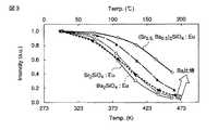
ピーク波長が約460nmの青色LED励起で蛍光体の発光波長と励起光の分離が困難な場合は、ピーク波長が約395nmの近紫外LEDにより励起を行ない、発光スペクトルの測定を実施した。具体的には、蛍光体のピーク波長が約545nm以下の際には、励起光と蛍光体の発光スペクトルの分離が困難なために、近紫外LEDにて励起を行なった。その結果を、図2に示す。Sr2SiO4:Eu蛍光体は、温度上昇に伴ない、徐々にピーク強度は低下し、130℃(403K)付近では室温の30%程度の強度となり、200℃(473K)付近では室温の5%以下の強度である。これに対し、Ba2SiO4:Eu蛍光体は、130℃付近では室温の40%程度の強度となり、200℃付近では室温の10%程度の強度である。温度特性は、Sr2SiO4:Eu蛍光体より、Ba2SiO4:Eu蛍光体のほうが良好であることが示されている。When it was difficult to separate the emission wavelength of the phosphor and the excitation light by exciting the blue LED having a peak wavelength of about 460 nm, excitation was performed with a near-ultraviolet LED having a peak wavelength of about 395 nm, and the emission spectrum was measured. Specifically, when the peak wavelength of the phosphor is about 545 nm or less, it is difficult to separate the excitation light and the emission spectrum of the phosphor, so excitation was performed with a near-ultraviolet LED. The result is shown in FIG. The peak intensity of the Sr2 SiO4 : Eu phosphor gradually decreases as the temperature rises. The intensity becomes about 30% of the room temperature near 130 ° C. (403 K), and 5% at room temperature near 200 ° C. (473 K). % Or less. On the other hand, the Ba2 SiO4 : Eu phosphor has an intensity of about 40% of room temperature near 130 ° C. and an intensity of about 10% of room temperature near 200 ° C. The temperature characteristics indicate that the Ba2 SiO4 : Eu phosphor is better than the Sr2 SiO4 : Eu phosphor.
さらに、(Sra,Bab,Caz,Euw)2SiO4蛍光体において、Ca含有量zを0に固定して二元系蛍光体を作製した。二元系蛍光体の作製に当たっては、Ba元素とSr元素との組成比を10%刻みで変化させた。得られた蛍光体の発光特性を評価したところ、Sr元素比、つまりa値が0から増加するにしたがって、ピーク波長が長波長化することが確認された。Furthermore, (Sr a, Ba b, Ca z, Eu w) in2 SiO4 phosphor, to produce a binary phosphor secure the Ca content z to zero. In producing the binary phosphor, the composition ratio of the Ba element and the Sr element was changed in increments of 10%. When the light emission characteristics of the obtained phosphor were evaluated, it was confirmed that the peak wavelength increased as the Sr element ratio, that is, the a value increased from 0.
一般に、Eu2+を発光中心元素として有する蛍光体のピーク波長の位置は、結晶格子内のEu2+位置が周りの陰イオンから受ける電場に大きく影響されて、変化することが知られている。(Sra,Bab,Caz,Euw)2SiO4蛍光体の場合も、アルカリ土類金属の組成によって発光波長が変化する。これは、混晶の結晶格子の大きさが組成によって変わり、Eu2+位置の電場が変わることが原因であると解釈される。アルカリ土類金属のイオン半径は、BaからSrと小さくなるので、結晶格子の大きさはこの順に小さくなって、Eu2+位置の電場がこの順に強くなる。その結果、Sr元素比、つまりa値が0から増加するにしたがって、発光ピーク波長が長くなる。In general, it is known that the position of the peak wavelength of a phosphor having Eu2+ as the luminescent central element changes depending on the electric field received from surrounding anions at the Eu2+ position in the crystal lattice. .(Sr a, Ba b, Ca z, Eu w) in the case of2 SiO4 phosphor, emission wavelength changes depending on the composition of the alkaline earth metals. This is interpreted to be caused by the fact that the size of the crystal lattice of the mixed crystal changes depending on the composition, and the electric field at the Eu2+ position changes. Since the ionic radius of the alkaline earth metal decreases from Ba to Sr, the size of the crystal lattice decreases in this order, and the electric field at the Eu2+ position increases in this order. As a result, the emission peak wavelength becomes longer as the Sr element ratio, that is, the a value increases from 0.
前述の種々の二元系蛍光体について、室温から200℃までの温度範囲において、温度変化にともなう発光強度の変化を評価した。その結果を、図3および図4に示す。図3は、a/(1−w):b/(1−w)=1:0〜0.5:0.5の組成を有する蛍光体の温度特性結果であり、図4は、a/(1−w):b/(1−w)=0.5:0.5〜0:1の組成を有する蛍光体の温度特性結果である。 The above-mentioned various binary phosphors were evaluated for changes in emission intensity with temperature changes in a temperature range from room temperature to 200 ° C. The results are shown in FIG. 3 and FIG. FIG. 3 is a temperature characteristic result of a phosphor having a composition of a / (1-w): b / (1-w) = 1: 0 to 0.5: 0.5, and FIG. It is a temperature characteristic result of a phosphor having a composition of (1-w): b / (1-w) = 0.5: 0.5 to 0: 1.
図3から、Sr2SiO4:Eu蛍光体からBa比が増加するにしたがって、温度特性が向上することがわかる。特に、Ba比がa/(1−w):b/(1−w)=0.5:0.5の組成である(Sr0.5,Ba0.5)2SiO4:Eu蛍光体は、温度特性が最高となる。しかしながら、a/(1−w):b/(1−w)=0.5:0.5を越えてBa比が増加した蛍光体では、Ba比が増加するにしたがって、温度特性が徐々に低下することが、図4に示されている。FIG. 3 shows that the temperature characteristics improve as the Ba ratio increases from the Sr2 SiO4 : Eu phosphor. In particular, (Sr0.5 , Ba0.5 )2 SiO4 : Eu phosphors having a Ba ratio of a / (1-w): b / (1-w) = 0.5: 0.5 have temperature characteristics. Is the best. However, in the phosphor having an increased Ba ratio exceeding a / (1-w): b / (1-w) = 0.5: 0.5, the temperature characteristics gradually increase as the Ba ratio increases. This is shown in FIG.
以上の結果から、(Sra,Bab,Caz,Euw)2SiO4蛍光体において、a/(1−w):b/(1−w)=0.8:0.2〜0.1:0.9の範囲の組成に規定することによって、Ba2SiO4:Eu蛍光体より温度特性が良好な蛍光体が得られることがわかった。Ba2SiO4:Eu蛍光体より良好な温度特性を有する(Sra,Bab,Caz,Euw)2SiO4蛍光体の存在は、本発明者らによって初めて見出されたものである。From the aboveresults, (Sr a, Ba b, Ca z, Eu w) in2 SiO4 phosphor, a / (1-w) : b / (1-w) = 0.8: 0.2~0 It was found that a phosphor having a temperature characteristic better than that of a Ba2 SiO4 : Eu phosphor can be obtained by defining the composition within a range of 0.1: 0.9. Ba2 SiO4: presence of from Eu phosphor having good temperature characteristic(Sr a, Ba b, Ca z, Eu w) 2 SiO 4 phosphor are those found for the first time by the present inventors .
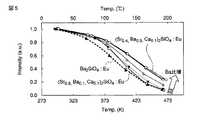
さらに、同様の製造方法によりBa−Sr−Ca比を変化させた三元系(Sra,Bab,Caz,Euw)2SiO4蛍光体を作製した。三元系蛍光体の作製に当たっては、Ca含有量(z値)を0.1に固定し、BaとSr元素の組成比を10%刻みで変化させた。得られた蛍光体の発光特性を評価したところ、Sr比、つまりa値が0から増加するにしたがって、ピーク波長が長波長化することが確認された。ただし、二元系蛍光体より、全体的に長波長のピーク波長であった。これは、z値が0.1であり、z=0の場合よりもCa組成の割合が多いことに起因するものと推測される。Furthermore, to produce ternary varying Ba-Sr-Ca ratio(Sr a, Ba b, Ca z, Eu w) of2 SiO4 phosphor by the same manufacturing method. In producing the ternary phosphor, the Ca content (z value) was fixed at 0.1, and the composition ratio of Ba and Sr elements was changed in increments of 10%. When the light emission characteristics of the obtained phosphor were evaluated, it was confirmed that the peak wavelength increased as the Sr ratio, that is, the a value increased from 0. However, the overall peak wavelength was longer than that of the binary phosphor. This is presumed to be due to the fact that the z value is 0.1 and the ratio of the Ca composition is higher than that in the case of z = 0.
前述の種々の三元系蛍光体について、室温から200℃までの温度範囲において、温度変化による発光強度の変化を評価した。その結果を、図5および図6に示す。図5は、a/(1−w):b/(1−w):z/(1−w)=0.8:0.1:0.1〜0.4:0.5:0.1の組成を有する蛍光体の温度特性結果であり、図6は、a/(1−w):b/(1−w):z/(1−w)=0.4:0.5:0.1〜0.1:0.8:0.1の組成を有する蛍光体の温度特性結果である。 The above-described various ternary phosphors were evaluated for changes in emission intensity due to temperature changes in a temperature range from room temperature to 200 ° C. The results are shown in FIG. 5 and FIG. FIG. 5 shows a / (1-w): b / (1-w): z / (1-w) = 0.8: 0.1: 0.1 to 0.4: 0.5: 0. 6 is a result of temperature characteristics of a phosphor having a composition of 1. FIG. 6 shows a / (1-w): b / (1-w): z / (1-w) = 0.4: 0.5: It is a temperature characteristic result of the fluorescent substance which has a composition of 0.1-0.1: 0.8: 0.1.
前述の図3の場合と同様に、Ba比が増加するにしたがって、温度特性が向上することが、図5からわかる。特に、a/(1−w):b/(1−w):z/(1−w)=0.4:0.5:0.1の組成である(Sr0.4,Ba0.5,Ca0.1)2SiO4:Eu蛍光体は、温度特性が最も良好となる。しかしながら、a/(1−w):b/(1−w):z/(1−w)=0.4:0.5:0.1の組成を超えてBa比が増加した組成を有する蛍光体では、Ba比が増加するに連れて温度特性が徐々に低下することが、図6に示されている。As in the case of FIG. 3 described above, it can be seen from FIG. 5 that the temperature characteristics improve as the Ba ratio increases. In particular, the composition is a / (1-w): b / (1-w): z / (1-w) = 0.4: 0.5: 0.1 (Sr0.4 , Ba0.5 , Ca0.1 The2 SiO4 : Eu phosphor has the best temperature characteristics. However, it has a composition in which the Ba ratio is increased beyond the composition of a / (1-w): b / (1-w): z / (1-w) = 0.4: 0.5: 0.1. It is shown in FIG. 6 that the temperature characteristics of the phosphor gradually decrease as the Ba ratio increases.
ただし、a/(1−w):b/(1−w):z/(1−w)=0.5:0.5:0の組成である(Sr0.5,Ba0.5)2SiO4:Eu蛍光体に匹敵した温度特性を有する三元系蛍光体は、存在しない。これは、図3および図4と図5および図6との比較から、次のように説明される。すなわち、三元系蛍光体の中で最も優れた温度特性を有するa/(1−w):b/(1−w):z/(1−w)=0.4:0.5:0.1の組成である(Sr0.4,Ba0.5,Ca0.1)2SiO4:Eu蛍光体は、温度上昇に伴なって、徐々にピーク強度が低下する。130℃(403K)付近では室温の60%程度の強度となり、200℃(473K)付近では室温の20%程度の強度である。これに対して、(Sr0.5,Ba0.5)2SiO4:Eu蛍光体は130℃付近では室温の80%程度の強度となり、200℃付近では室温の40%程度の強度であることからわかる。したがって、Ca比(z値)が増加すると、温度特性は低下するものと推測される。However, the composition is a / (1-w): b / (1-w): z / (1-w) = 0.5: 0.5: 0 (Sr0.5 , Ba0.5 )2 SiO4 : There are no ternary phosphors having temperature characteristics comparable to Eu phosphors. This is explained as follows from the comparison between FIG. 3 and FIG. 4 and FIG. 5 and FIG. That is, a / (1-w): b / (1-w): z / (1-w) = 0.4: 0.5: 0 having the most excellent temperature characteristics among the ternary phosphors. The peak intensity of the (Sr0.4 , Ba0.5 , Ca0.1 )2 SiO4 : Eu phosphor having a composition of .1 gradually decreases with increasing temperature. In the vicinity of 130 ° C. (403 K), the strength is about 60% of the room temperature, and in the vicinity of 200 ° C. (473 K), the strength is about 20% of the room temperature. In contrast, the (Sr0.5 , Ba0.5 )2 SiO4 : Eu phosphor has an intensity of about 80% of room temperature near 130 ° C., and an intensity of about 40% of room temperature near 200 ° C. Therefore, when the Ca ratio (z value) increases, it is estimated that the temperature characteristics deteriorate.
以上の結果から、(Sra,Bab,Caz,Euw)2SiO4蛍光体において、a/(1−w):b/(1−w):z/(1−w)=0.7:0.2:0.1〜0.2:0.7:0.1の範囲に組成を規定することによって、Ba2SiO4:Eu蛍光体より温度特性が良好な蛍光体が得られることがわかった。From the aboveresults, (Sr a, Ba b, Ca z, Eu w) in2 SiO4 phosphor, a / (1-w) : b / (1-w): z / (1-w) = 0 By defining the composition within the range of 7: 0.2: 0.1 to 0.2: 0.7: 0.1, a phosphor having better temperature characteristics than the Ba2 SiO4 : Eu phosphor can be obtained. I found out that
良好な温度特性が得られる理由は、次のように推測される。一般的に、蛍光体は温度が上昇すると発光効率が低下すること(温度消光)が知られている。上述のように組成が規定されたユーロピウム付活正ケイ酸アルカリ土類蛍光体は、温度が上昇したときの発光効率の低下が少なく、消光温度が高められる。温度消光に影響を及ぼす因子としては、発光中心イオンの大きさとこれが置換する蛍光体母体イオンの大きさとの違い、および蛍光体母体の結晶格子安定性などが挙げられる。上述の蛍光体においては、発光中心イオンはEuイオンであり、母材は(Sra,Bab,Caz)2SiO4で表わされる組成の正ケイ酸アルカリ土類化合物である。The reason why good temperature characteristics can be obtained is presumed as follows. In general, it is known that phosphors have lower luminous efficiency (temperature quenching) when the temperature rises. As described above, the europium-activated alkaline earth silicate phosphor having a defined composition has little decrease in light emission efficiency when the temperature rises, and the quenching temperature is increased. Factors affecting temperature quenching include the difference between the size of the luminescent center ion and the size of the phosphor host ion that it replaces, and the crystal lattice stability of the phosphor host. In the phosphor described above, the luminescent center ion is Eu ion, which is a base material(Sr a, Ba b, Ca z) alkaline earth ortho-silicate compound having a composition represented by2 SiO4.
(Sra,Bab,Caz,Euw)2SiO4蛍光体の格子定数を求めたところ、上述した組成範囲は、まさにBa2SiO4→Sr2SiO4結晶構造の変局点付近の組成であることが判明した。すなわち、こうした組成範囲では、格子定数の変化が大きいことになる。(Sra,Bab,Caz,Euw)2SiO4蛍光体の組成変化に伴なうSr2SiO4結晶の(hkl)面指数、(400)、(020)、(004)の格子面間隔の変化を、下記表1にまとめる。It was determined for(Sr a, Ba b, Ca z, Eu w) 2 lattice constant of SiO4 phosphor, the above-mentioned composition range, very near the inflection point of Ba2 SiO4 → Sr2 SiO4 crystal structure It turned out to be a composition. That is, in such a composition range, the change in lattice constant is large.(Sr a, Ba b, Ca z, Eu w) 2 composition change of SiO4 phosphor accompanied Sr2 SiO4 crystal (hkl) plane index grating (400), (020), (004) Table 1 below summarizes the change in the surface spacing.
蛍光体の格子定数は、以下の手法により求めた。まず、蛍光体サンプルについて、粉末X線回折分析法(X−ray diffractometry:XRD)により回折パターンを測定した。測定には、マック・サイエンス社(ブルーカー・エイエックスエス(株))M18XHF22−SRA等を用いた。得られた回折パターンを、JCPDS(Joint Committee on Powder Diffraction Standards)カードにおける該当するカードパターンと比較した。Sr2SiO4結晶相は(#39−1256)のカードパターンと比較し、Ba2SiO4結晶相は(#26−1403))のカードパターンと比較して、(hkl)面指数に一致すると推測されるピークより格子面間隔を求めた。具体的には、Sr2SiO4結晶相では(400)、(020)、(004)の格子面間隔に一致すると推測されるピークより格子面間隔を求めた。Ba2SiO4結晶相では、(400)、(040)、(002)の格子面間隔に一致すると推測されるピークより格子面間隔を求めた。こうして得られた格子面間隔から、単位格子の体積を計算した。The lattice constant of the phosphor was determined by the following method. First, a diffraction pattern of the phosphor sample was measured by powder X-ray diffraction analysis (XRD). For the measurement, Mac Science Co., Ltd. (Blue Car AXS Co., Ltd.) M18XHF22 -SRA or the like was used. The obtained diffraction pattern was compared with the corresponding card pattern in a JCPDS (Joint Committee on Powder Diffraction Standards) card. When the Sr2 SiO4 crystal phase is compared with the card pattern of (# 39-1256) and the Ba2 SiO4 crystal phase is compared with the card pattern of (# 26-1403), it matches the (hkl) plane index. The lattice spacing was determined from the estimated peak. Specifically, in the Sr2 SiO4 crystal phase, the lattice plane spacing was obtained from the peak estimated to coincide with the lattice spacing of (400), (020), (004). In the Ba2 SiO4 crystal phase, the lattice plane spacing was obtained from the peak estimated to coincide with the lattice spacing of (400), (040), (002). From the lattice spacing obtained in this way, the volume of the unit cell was calculated.
各元素の含有量を分析するにあたっては、まず、合成した蛍光体をアルカリ融解した。得られた融解液を、例えばエスアイアイ・ナノテクノロジー社 SPS1200AR等により内部標準のICP発光分光法にて分析を行なって、各元素の含有量を得た。
上記表1で測定した格子面間隔に基づいて、(Sra,Bab,Caz,Euw)2SiO4蛍光体の組成変化と、これに伴なう単位格子の体積変化との関係を求めた。その結果を、図7に示す。図示するように、b/(1−w)=0.5から0.6付近で体積が大きく増加していることが示されている。可能性として、この体積の急な増加が確認される組成が起因して、消光温度が高められたものと推測される。Based on the lattice spacing, measured in the above Table1, (Sr a, Ba b , Ca z, Eu w) the composition change of2 SiO4 phosphor, to which the relationship between the volume change accompanying the unit cell Asked. The result is shown in FIG. As shown in the figure, it is shown that the volume greatly increases in the vicinity of b / (1−w) = 0.5 to 0.6. As a possibility, the extinction temperature is presumed to be increased due to the composition in which the sudden increase in volume is confirmed.
上述したような組成の蛍光体粒子の表面には、シリコーン樹脂、エポキシ樹脂、フッ素樹脂、テトラエトキシシラン(TEOS)、シリカ、ケイ酸亜鉛、ケイ酸アルミニウム、カルシウムポリフォスフェート、シリコーンオイル、およびシリコーングリースから選択される少なくとも一種からなる表層材を配置することができる。これによって、蛍光体の防湿性が高められる。 On the surface of the phosphor particles having the composition as described above, silicone resin, epoxy resin, fluororesin, tetraethoxysilane (TEOS), silica, zinc silicate, aluminum silicate, calcium polyphosphate, silicone oil, and silicone A surface layer material made of at least one selected from grease can be disposed. This improves the moisture resistance of the phosphor.
ケイ酸亜鉛およびケイ酸アルミニウムは、例えばZnO・cSiO2(1≦c≦4)、およびAl2O3・dSiO2(1≦d≦10)でそれぞれ表わされる。表層材は蛍光体粒子表面が完全に覆われている必要はなく、その一部が露出していてもよい。蛍光体粒子の表面に、上述したような材質からなる表層材が存在していれば、その効果が得られる。表層材は、その分散液または溶液を用いて蛍光体粒子表面に配置することができる。分散液または溶液中に粒子を所定時間浸漬した後、加熱等により乾燥させることによって表層材が配置される。蛍光体としての本来の機能を損なうことなく、防湿性向上という表層材の効果を得るために、表層材は、蛍光体粒子の0.1〜5%程度の体積割合で存在することが好ましい。Zinc silicate and aluminum silicate are represented by, for example, ZnO · cSiO2 (1 ≦ c ≦ 4) and Al2 O3 · dSiO2 (1 ≦ d ≦ 10), respectively. The surface layer material does not need to be completely covered with the surface of the phosphor particles, and a part thereof may be exposed. If a surface layer material made of the above-described material is present on the surface of the phosphor particles, the effect can be obtained. The surface layer material can be disposed on the surface of the phosphor particles using the dispersion or solution. After immersing the particles in the dispersion or solution for a predetermined time, the surface layer material is disposed by drying by heating or the like. In order to obtain the effect of the surface material of improving the moisture resistance without impairing the original function as the phosphor, the surface material is preferably present in a volume ratio of about 0.1 to 5% of the phosphor particles.
上記一般式(1)で表わされる組成を有する蛍光体は、例えば、波長440nm〜480nmの青色領域に発光ピークを有する発光素子と組み合わせて発光装置を作製することができる。発光素子としては、青色LEDおよびレーザーダイオードのいずれを用いてもよい。波長360nm〜440nmの近紫外線から紫色領域に発光ピークを有する発光素子もまた、用いることができる。発光素子の種類によらず、色ずれが少なく、発光特性の優れた発光装置を得ることができる。 For example, the phosphor having the composition represented by the general formula (1) can be combined with a light emitting element having a light emission peak in a blue region having a wavelength of 440 nm to 480 nm to produce a light emitting device. Either a blue LED or a laser diode may be used as the light emitting element. A light-emitting element having a light emission peak in the violet region from near ultraviolet rays having a wavelength of 360 nm to 440 nm can also be used. Regardless of the type of light-emitting element, a light-emitting device with little color shift and excellent light-emitting characteristics can be obtained.
上述のように組成が規定された蛍光体は、温度特性が良好であるので、ジャンクション温度の高い発光素子を組み合わせることによって、その効果が特に発揮される。こうした組み合わせによって得られるのが、本発明の実施形態にかかる発光装置である。 Since the phosphor whose composition is defined as described above has good temperature characteristics, the effect is particularly exhibited by combining a light emitting element having a high junction temperature. The light emitting device according to the embodiment of the present invention is obtained by such a combination.
上記一般式(1)で表わされる組成を有する蛍光体は、青色蛍光体および赤色蛍光体と組み合わせて使用することができる。例えば、青色領域の光源を使用する場合には、上記一般式(1)で表わされる組成の蛍光体と赤色蛍光体とを組み合わせることによって、色温度の低い白色発光装置が得られる。また、近紫外領域の光源を使用する場合には、上記一般式(1)で表わされる組成の蛍光体に加えて、青色蛍光体および赤色蛍光体と組み合わせることによって白色発光装置が得られる。 The phosphor having the composition represented by the general formula (1) can be used in combination with a blue phosphor and a red phosphor. For example, when a blue light source is used, a white light emitting device having a low color temperature can be obtained by combining a phosphor having a composition represented by the general formula (1) and a red phosphor. When a light source in the near ultraviolet region is used, a white light emitting device can be obtained by combining with a blue phosphor and a red phosphor in addition to the phosphor having the composition represented by the general formula (1).
青色蛍光体としては、例えば、BaMgAl10O17:Eu蛍光体や(Ca,Sr,Ba)5(PO4)3Cl:Eu蛍光体などを用いることができる。また、赤色蛍光体としては、例えば(Srx,Bay,Caz,Euw)2SiO4蛍光体や3.5MgO・0.5MgF2・GeO2:Mn蛍光体や(Ba,Sr,Ca)2Si5N8:Eu蛍光体、(Sr,Ca)SiN2:Eu蛍光体、(Sr,Ca)AlSiN3:Eu蛍光体などを用いることができる。特に、(Ba,Sr,Ca)2Si5N8:Eu蛍光体や(Sr,Ca)AlSiN3:Eu蛍光体などの窒化物蛍光体が好ましい。こうした窒化物蛍光体は、温度特性が良好であるので、色ずれが少なく、発光特性の優れたより好ましい発光装置が得られる。As the blue phosphor, for example, BaMgAl10 O17 : Eu phosphor, (Ca, Sr, Ba)5 (PO4 )3 Cl: Eu phosphor, or the like can be used. Further, as the red phosphor, for example,(Sr x, Ba y, Ca z, Eu w) 2 SiO 4 phosphor and3.5MgO · 0.5MgF 2 · GeO 2: Mn phosphor and (Ba, Sr, Ca )2 Si5 N8 : Eu phosphor, (Sr, Ca) SiN2 : Eu phosphor, (Sr, Ca) AlSiN3 : Eu phosphor, and the like can be used. In particular, nitride phosphors such as (Ba, Sr, Ca)2 Si5 N8 : Eu phosphor and (Sr, Ca) AlSiN3 : Eu phosphor are preferable. Since such a nitride phosphor has good temperature characteristics, a more preferable light-emitting device with less color shift and excellent light-emitting characteristics can be obtained.
図8には、本発明の一実施形態にかかる発光装置の断面を示す。 In FIG. 8, the cross section of the light-emitting device concerning one Embodiment of this invention is shown.
図示する発光装置は、樹脂ステム200はリードフレームを成形してなるリード201およびリード202と、これに一体成形されてなる樹脂部203とを有する。樹脂部203は、上部開口部が底面部より広い凹部205を有しており、この凹部の側面には反射面204が設けられる。反射面204は、樹脂部203の凹部の側面に、アルミナなどの部材を塗布して作製することができ、発光した光の取り出しを高める作用を有する。 In the illustrated light emitting device, the
凹部205の略円形底面中央部には、発光チップ206がAgペースト等によりマウントされている。発光チップ206としては、360nmを越え500nm以下の波長領域に主発光ピークを有し、ジャンクション温度が125℃以上のものが用いられる。例えば、GaAs系、GaN系等の半導体発光ダイオード等を用いることが可能である。発光チップ206の電極(図示せず)は、Auなどからなるボンディングワイヤ207および208によって、リード201およびリード202にそれぞれ接続されている。なお、リード201および202の配置は、適宜変更することができる。 A
樹脂部203の凹部205内には、蛍光体210が分散された樹脂層211からなる蛍光体層209が配置される。樹脂層211としては、例えばシリコーン樹脂の硬化物を用いることができ、蛍光体210は、この樹脂層211中に、例えば5wt%以上50wt%以下の割合で分散することができる。蛍光体210の少なくとも一部は、上述したように組成が規定されたユーロピウム付活正ケイ酸アルカリ土類蛍光体である。蛍光体は、有機材料である樹脂や無機材料であるガラスなど種々のバインダーにより、付着させることができる。 A
有機材料のバインダーとしては、上述したシリコーン樹脂の他にエポキシ樹脂、アクリル樹脂など耐光性に優れた透明樹脂が適している。無機材料のバインダーとしてはアルカリ土類ホウ酸塩等を使用した低融点ガラス等、粒径の大きな蛍光体を付着させるために超微粒子のシリカ、アルミナ等、沈殿法により得られるアルカリ土類リン酸塩等が適している。これらのバインダーは、単独でも2種以上を組み合わせて用いてもよい。 As the binder for the organic material, a transparent resin excellent in light resistance such as an epoxy resin and an acrylic resin is suitable in addition to the above-described silicone resin. Low-melting glass using alkaline earth borate or the like as a binder for inorganic materials, such as ultrafine silica, alumina, etc., for attaching phosphors with large particle diameter, alkaline earth phosphate obtained by precipitation method Salt etc. are suitable. These binders may be used alone or in combination of two or more.
また、蛍光体層に使用される蛍光体には、必要に応じて表面にコーティング処理を施すことができる。この表面コーティングにより、蛍光体が熱、湿度、紫外線等の外的要因から劣化が防止される。さらに、蛍光体の分散性を調整することが可能となり、蛍光体層の設計を容易に行なうことができる。 The phosphor used in the phosphor layer can be coated on the surface as necessary. This surface coating prevents the phosphor from being deteriorated by external factors such as heat, humidity, and ultraviolet rays. Further, the dispersibility of the phosphor can be adjusted, and the phosphor layer can be easily designed.
発光チップ206としては、n型電極とp型電極とを同一面上に有するフリップチップ型のものを用いることも可能である。この場合には、ワイヤの断線や剥離、ワイヤによる光吸収等のワイヤに起因した問題を解消して、信頼性の高い高輝度な半導体発光装置が得られる。また、発光チップ206にn型基板を用いて、次のような構成とすることもできる。具体的には、n型基板の裏面にn型電極を形成し、基板上の半導体層上面にはp型電極を形成して、n型電極またはp型電極をリードにマウントする。p型電極またはn型電極は、ワイヤにより他方のリードに接続することができる。発光チップ206のサイズ、凹部205の寸法および形状は、適宜変更することができる。 As the
図9には、本発明の他の実施形態にかかる発光装置の断面図を示す。図示する発光装置は、樹脂ステム100と、その上にマウントされた半導体発光素子106Fと、この半導体発光素子106Fを覆う封止体111とを有する。封止樹脂ステム100は、リードフレームから形成されたリード101、102と、これと一体的に成型されてなる樹脂部103とを有する。リード101、102は、それぞれの一端が近接対向するように配置されている。リード101、102の他端は、互いに反対方向に延在し、樹脂部103から外部に導出されている。 FIG. 9 shows a cross-sectional view of a light emitting device according to another embodiment of the present invention. The illustrated light-emitting device includes a
樹脂部103には開口部105が設けられ、開口部の底面には、保護用ツェナー・ダイオード106Eが接着剤107によってマウントされている。保護用ツェナー・ダイオード106Eの上には、半導体発光素子106Fが実装されている。すなわち、リード101の上にダイオード106Eがマウントされている。ダイオード106Eからリード102にワイヤ109が接続されている。なお、半導体発光素子106Fは、360nmを越え500nm以下の波長領域に主発光ピークを有し、ジャンクション温度が125℃以上である。 An
半導体発光素子106Fは、樹脂部103の内壁面に取り囲まれており、この内壁面は光取り出し方向に向けて傾斜し、光を反射する反射面104として作用する。開口部105内に充填された封止体111は、蛍光体110を含有している。半導体発光素子106Fは、保護用ツェナー・ダイオード106Eの上に積層されている。蛍光体110の少なくとも一部は、上述したように組成が規定されたユーロピウム付活正ケイ酸アルカリ土類蛍光体である。 The semiconductor
以下に、発光装置のチップ周辺部分について詳細に説明する。図10に示されるように、保護用ダイオード106Eは、n型シリコン基板150の表面にp型領域152が形成されたプレーナ構造を有する。p型領域152にはp側電極154が形成され、基板150の裏面にはn側電極156が形成されている。このn側電極156に対向して、ダイオード106Eの表面にもn側電極158が形成されている。こうした2つのn側電極156と158とは、ダイオード106Eの側面に設けられた配線層160によって接続される。さらに、p側電極154およびn側電極158が設けられたダイオード106Eの表面には、高反射膜162が形成されている。高反射膜162は、発光素子106Fから放出される光に対して高い反射率を有する膜である。 Hereinafter, a chip peripheral portion of the light emitting device will be described in detail. As shown in FIG. 10, the protective diode 106 </ b> E has a planar structure in which a p-
半導体発光素子106Fにおいては、バッファ層122、n型コンタクト層123、n型クラッド層132、活性層124、p型クラッド層125、およびp型コンタクト層126が、透光性基板138の上に順次積層されている。さらに、n側電極127がn型コンタクト層123の上に形成され、p側電極128がp型コンタクト層126の上に形成されている。活性層124から放出される光は、透光性基板138を透過して取り出される。 In the semiconductor
このような構造の発光素子106Fは、バンプを介してダイオード106Eにフリップ・チップ・マウントされている。具体的には、バンプ142によって、発光素子106Fのp側電極128がダイオード106Eのn側電極158に電気的に接続されている。また、バンプ144によって、発光素子106Fのn側電極127が、ダイオード106Eのp側電極154に電気的に接続されている。ダイオード106Eのp側電極154には、ワイヤ109がボンディングされ、このワイヤ109はリード102に接続されている。 The
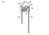
図11には、砲弾型の発光装置の例を示す。半導体発光素子51は、リード50’にマウント材52を介して実装され、プレディップ材54で覆われる。ここで用いられる半導体発光素子51は、360nmを越え500nm以下の波長領域に主発光ピークを有し、ジャンクション温度が125℃以上である。ワイヤ53により、リード50が半導体発光素子51に接続され、キャスティング材55で封入されている。プレディップ材54中には、蛍光体が含有され、その少なくとも一部は、上述したように組成が規定されたユーロピウム付活正ケイ酸アルカリ土類蛍光体である。 FIG. 11 shows an example of a bullet-type light emitting device. The semiconductor
上記一般式(1)で表わされる組成を有する蛍光体は、温度特性が良好であるので、ジャンクション温度の高い発光素子と組み合わせることによって、色ずれが少なく、優れた発光特性を有する発光装置が得られる。 Since the phosphor having the composition represented by the general formula (1) has good temperature characteristics, a light emitting device having excellent light emission characteristics with little color shift is obtained by combining with a light emitting element having a high junction temperature. It is done.
以下、実施例および比較例を示して本発明をさらに詳細に説明するが、本発明はその趣旨を超えない限り、以下の実施例に限定されるものではない。 EXAMPLES Hereinafter, although an Example and a comparative example are shown and this invention is demonstrated further in detail, this invention is not limited to a following example, unless the meaning is exceeded.
(Sr0.45,Ba0.45,Eu0.1)2SiO4蛍光体を調製した。原料粉末としては、SrCO3粉末11.96g、BaCO3粉末15.98g、SiO2粉末5.71g、およびEu2O3粉末3.17gを用意した。さらに、結晶成長剤として、0.3gのNH4Clを添加して、ボールミルで均一に混合した。(Sr0.45 , Ba0.45 , Eu0.1 )2 SiO4 phosphor was prepared. As raw material powders, 11.96 g of SrCO3 powder, 15.98 g of BaCO3 powder, 5.71 g of SiO2 powder, and 3.17 g of Eu2 O3 powder were prepared. Further, 0.3 g of NH4 Cl was added as a crystal growth agent and mixed uniformly with a ball mill.
得られた混合原料を焼成容器に収容し、以下の焼成条件で焼成した。まず、N2/H2の還元性雰囲気中、1000℃〜1600℃で3〜7時間焼成して、一次焼成品を得た。これを粉砕して再び坩堝に収容し、炉内に配置して、炉内を真空で窒素置換した。さらに、水素濃度5%以上99%未満のN2/H2の還元性雰囲気中、1000℃〜1600℃で2〜6時間焼成して、二次焼成品を得た。The obtained mixed raw material was accommodated in a firing container and fired under the following firing conditions. First, firing was performed at 1000 ° C. to 1600 ° C. for 3 to 7 hours in a reducing atmosphere of N2 / H2 to obtain a primary fired product. This was pulverized and again stored in a crucible, placed in a furnace, and the inside of the furnace was purged with nitrogen under vacuum. Furthermore, it was baked at 1000 ° C. to 1600 ° C. for 2 to 6 hours in a reducing atmosphere of N2 / H2 having a hydrogen concentration of 5% or more and less than 99% to obtain a secondary baked product.
得られた二次焼成品を水中で粉砕、篩後、吸引ろ過により脱水した。最後に、乾燥機中150℃で乾燥し、さらに篩を通して、No.1の蛍光体を合成した。得られた蛍光体をICP発光分光法により定量分析を実施した結果、ほぼ仕込みどおりの組成であることを確認した。 The obtained secondary fired product was pulverized in water, sieved, and dehydrated by suction filtration. Finally, it was dried in a dryer at 150 ° C., passed through a sieve, 1 phosphor was synthesized. As a result of quantitative analysis of the obtained phosphor by ICP emission spectroscopy, it was confirmed that the composition was almost as prepared.
さらに、下記表2に示すように各構成元素の含有量を変化させて、No.2〜10の蛍光体を作製した。No.9の蛍光体にはSrが含有されず、No.10の蛍光体にはBaが含有されない。
No.1の(Sr0.45,Ba0.45,Eu0.1)2SiO4蛍光体と、市販のCaAlSiN3:Eu蛍光体を混合し、シリコーン樹脂に分散させて樹脂混合物を調製した。この樹脂混合物とLEDチップと支持部材とを用いて、白色LED発光装置を作製した。LEDチップは、ジャンクション温度が180℃であり、ピーク波長が465nmである。支持部材は、Cu製のカップ状で、側面内壁には光反射率の高いアルミナが塗布されており、外部との電気的接続を保つ機能を備えている。LEDチップは、Cu製支持部材の底面にはんだ接合して、フリップチップ型白色LED発光装置を作製した。No. 1 (Sr0.45 , Ba0.45 , Eu0.1 )2 SiO4 phosphor and a commercially available CaAlSiN3 : Eu phosphor were mixed and dispersed in a silicone resin to prepare a resin mixture. Using this resin mixture, the LED chip, and the support member, a white LED light emitting device was produced. The LED chip has a junction temperature of 180 ° C. and a peak wavelength of 465 nm. The support member is in the shape of a cup made of Cu, and the side wall is coated with alumina having a high light reflectivity, and has a function of maintaining electrical connection with the outside. The LED chip was soldered to the bottom surface of the Cu support member to produce a flip chip type white LED light emitting device.
この白色LED発光装置の熱抵抗は33℃/Wであった。この白色LED装置を実施例1とする。 The white LED light-emitting device had a thermal resistance of 33 ° C./W. This white LED device is referred to as Example 1.
色温度は4200Kとなるように、蛍光体の混合割合を調整した。実施例1の白色LED発光装置を環境温度35℃において、投入電力3.8Wで駆動した。駆動直後の発光スペクトルを、図12に示す。図12のスペクトルにおいては、500nm以上600nm以下、具体的には、540nm近傍に主発光ピークが示されている。このときの色度値は、x=0.372、y=0.372であった。 The mixing ratio of the phosphors was adjusted so that the color temperature was 4200K. The white LED light emitting device of Example 1 was driven at an input power of 3.8 W at an environmental temperature of 35 ° C. The emission spectrum immediately after driving is shown in FIG. In the spectrum of FIG. 12, a main emission peak is shown in the range of 500 nm to 600 nm, specifically, around 540 nm. The chromaticity values at this time were x = 0.372 and y = 0.372.
さらに、実施例1の白色LED発光装置を1時間駆動させて、発光スペクトルを測定した。その結果を、図13に示す。このときの色度値はx=0.365、y=0.314であり、色温度は約3920Kに変化していた。図12のスペクトルと同様、図13のスペクトルにおいても、500nm以上600nm以下、具体的には、530nm近傍に主発光ピークが示されている。1時間駆動させることによって、(Sr0.45,Ba0.45,Eu0.1)2SiO4蛍光体部分のピーク強度高さは、駆動直後より低下するものの、57%は保たれることが図12と図13との比較から確認された。Furthermore, the white LED light-emitting device of Example 1 was driven for 1 hour, and the emission spectrum was measured. The result is shown in FIG. The chromaticity values at this time were x = 0.365, y = 0.314, and the color temperature was changed to about 3920K. Similar to the spectrum of FIG. 12, the main emission peak is also shown in the spectrum of FIG. 13 in the range of 500 nm to 600 nm, specifically near 530 nm. By driving for 1 hour, the peak intensity height of the (Sr0.45 , Ba0.45 , Eu0.1 )2 SiO4 phosphor portion is lower than that immediately after driving, but 57% is maintained. It was confirmed from the comparison.
次に、No.9の(Ba0.9,Eu0.1)2SiO4蛍光体と市販の赤色窒化物蛍光体CaAlSiN3:Eu蛍光体とを混合し、シリコーン樹脂に分散させて樹脂混合物を調製した。この樹脂混合物を用いる以外は前述と同様にして、比較例1の白色LED発光装置を作製した。この白色LED発光装置の熱抵抗は34℃/Wであった。色温度は4200Kとなるように蛍光体の混合割合を調整した。Next, no. 9 (Ba0.9 , Eu0.1 )2 SiO4 phosphor and a commercially available red nitride phosphor CaAlSiN3 : Eu phosphor were mixed and dispersed in a silicone resin to prepare a resin mixture. A white LED light-emitting device of Comparative Example 1 was produced in the same manner as described above except that this resin mixture was used. The thermal resistance of this white LED light-emitting device was 34 ° C./W. The mixing ratio of the phosphors was adjusted so that the color temperature was 4200K.
比較例1の白色LED発光装置を環境温度35℃において、投入電力3.8Wで駆動した。駆動直後の発光スペクトルを、図14に示す。このときの色度値は、x=0.372、y=0.372であった。図14のスペクトルにおいては、(Ba0.9,Eu0.1)2SiO4蛍光体による発光は、515nm近傍に主発光ピークが示されている。The white LED light-emitting device of Comparative Example 1 was driven at an ambient temperature of 35 ° C. with an input power of 3.8 W. The emission spectrum immediately after driving is shown in FIG. The chromaticity values at this time were x = 0.372 and y = 0.372. In the spectrum of FIG. 14, the main emission peak is shown in the vicinity of 515 nm for the light emission by the (Ba0.9 , Eu0.1 )2 SiO4 phosphor.
さらに、比較例1の白色LED発光装置を1時間駆動させて、発光スペクトルを測定した。その結果を、図15に示す。このときの色度値はx=0.449、y=0.271であり、色温度は約1700Kに変化していた。図14と同様に図15のスペクトルにおいても、(Ba0.9,Eu0.1)2SiO4蛍光体による発光は、510nm近傍に主発光ピークが示されている。1時間駆動させることによって、(Ba0.9,Eu0.1)2SiO4蛍光体部分のピーク強度高さは、駆動直後の20%まで低下することが、図14と図15との比較から確認された。Furthermore, the white LED light-emitting device of Comparative Example 1 was driven for 1 hour, and the emission spectrum was measured. The result is shown in FIG. The chromaticity values at this time were x = 0.449 and y = 0.271, and the color temperature was changed to about 1700K. Similarly to FIG. 14, in the spectrum of FIG. 15, light emission by the (Ba0.9 , Eu0.1 )2 SiO4 phosphor shows a main emission peak in the vicinity of 510 nm. It was confirmed from the comparison between FIG. 14 and FIG. 15 that the peak intensity height of the (Ba0.9 , Eu0.1 )2 SiO4 phosphor portion decreased to 20% immediately after driving by driving for 1 hour. .
実施例1と比較例1との比較から、次のことが明らかである。いずれの白色LED発光装置においても、長時間駆動させた後には、LEDチップ近傍の温度が上昇する。実施例1の白色LED発光装置においては、用いた蛍光体の温度特性が良好なので、長時間駆動させても、発光ピーク強度は57%程度維持される。このため、ピーク強度の減少に起因した色度値や色温度のずれも小さい。 From the comparison between Example 1 and Comparative Example 1, the following is clear. In any white LED light emitting device, the temperature in the vicinity of the LED chip rises after being driven for a long time. In the white LED light-emitting device of Example 1, since the temperature characteristics of the phosphor used are good, the emission peak intensity is maintained at about 57% even when driven for a long time. For this reason, deviations in chromaticity values and color temperatures due to a decrease in peak intensity are also small.
これに対して、比較例1の白色LED発光装置で用いられた蛍光体は、温度特性が乏しいため、長時間駆動した後には、発光ピーク強度が20%まで大きく減少している。その結果、色度および色温度のずれも大きい。 On the other hand, since the phosphor used in the white LED light emitting device of Comparative Example 1 has poor temperature characteristics, the emission peak intensity is greatly reduced to 20% after being driven for a long time. As a result, the deviations in chromaticity and color temperature are also large.
さらに、下記表3に示すように発光素子と蛍光体とを組み合わせて、実施例2〜8、および比較例2の発光装置を作製した。実施例2〜8の発光装置においては、No.2〜8のいずれかの蛍光体を含む蛍光体混合物を用い、比較例2においては、No.10の蛍光体を含む蛍光体混合物を用いた。 Furthermore, as shown in Table 3 below, light emitting devices of Examples 2 to 8 and Comparative Example 2 were fabricated by combining light emitting elements and phosphors. In the light emitting devices of Examples 2 to 8, No. A phosphor mixture containing any one of the phosphors 2 to 8 was used. A phosphor mixture containing 10 phosphors was used.
いずれにおいても、発光装置の色温度が4200Kとなるように、蛍光体の混合割合を調整し、シリコーン樹脂に分散させた。発光素子としてはジャンクション温度が180℃のLEDチップを使用した。LEDチップは、前述と同様のCu製支持部材の底面にはんだ接合して、フリップチップ型白色LED発光装置を作製した。
各白色LED発光装置を環境温度25℃において、投入電力3.0Wで駆動し、駆動直後の色度値、色温度、および発光ピーク強度を調べた。さらに、同様の発光装置を同様の条件で1時間駆動させて、駆動直後の色度値、色温度、および発光ピーク強度を調べた。駆動直後および1時間駆動後のピーク強度から、ピーク強度維持率を求め、色度値および色温度とともに、下記表4にまとめる。
上記表4に示されるように、実施例の発光装置においては、いずれも用いた蛍光体の温度特性が良好なので、1時間駆動させても、発光ピーク強度の低下は30%程度にとどまる。このため、ピーク強度の減少に起因した色度値や色温度のずれも小さい。 As shown in Table 4 above, since the temperature characteristics of the phosphors used in all of the light emitting devices of the examples are good, even when driven for 1 hour, the decrease in emission peak intensity is only about 30%. For this reason, deviations in chromaticity values and color temperatures due to a decrease in peak intensity are also small.
これに対して、比較例2の白色LED発光装置で用いられた蛍光体は、温度特性が乏しいため、長時間駆動した後には、発光ピーク強度が25%まで大きく減少している。その結果、色度および色温度のずれも大きい。 On the other hand, since the phosphor used in the white LED light emitting device of Comparative Example 2 has poor temperature characteristics, the emission peak intensity greatly decreases to 25% after being driven for a long time. As a result, the deviations in chromaticity and color temperature are also large.
本発明の実施形態にかかる発光装置は、照明用光源、LEDディスプレイ、パソコンや携帯電話機等のバックライト光源、信号機、照明スイッチ、車載用ストップランプ、各種センサーおよび各種インジケータ等、各種照明装置や各種表示装置などに利用することができる。 A light emitting device according to an embodiment of the present invention includes a lighting source, an LED display, a backlight source such as a personal computer and a mobile phone, a traffic light, a lighting switch, a vehicle-mounted stop lamp, various sensors, various indicators, and various lighting devices and various types. It can be used for display devices.
200…樹脂ステム; 201…リード; 202…リード; 203…樹脂部
204…反射面; 205…凹部; 206…発光チップ
207…ボンディングワイヤ; 208…ボンディングワイヤ; 209…蛍光体層
210…蛍光体; 211…樹脂層; 100…樹脂ステム; 101…リード
102…リード; 103…樹脂部; 104…反射面; 105…開口部
106E…ツェナー・ダイオード; 106F…半導体発光素子; 107…接着剤
109…ボンディングワイヤ; 110…蛍光体; 111…封止体
122…バッファ層; 123…n型コンタクト層; 124…活性層
125…p型クラッド層; 126…p型コンタクト層; 127…n側電極
128…p側電極; 132…n型クラッド層; 138…透光性基板
142…バンプ; 144…バンプ; 150…n型シリコン基板
152…p型領域; 154…p側電極; 156…n側電極; 158…n側電極
160…配線層; 162…高反射膜; 50…リード; 50’…リード
51…半導体発光素子; 52…マウント材; 53…ボンディングワイヤ
54…プレディップ材; 55…キャスティング材。DESCRIPTION OF
Claims (10)
Translated fromJapanese前記発光素子から発せられる光を受ける蛍光体を含む蛍光体層とを具備する発光装置であって、
前記発光素子のジャンクション温度は125℃以上であり、
前記蛍光体の少なくとも一部は、前記発光素子が放つ光を吸収して500nm以上600nm以下の波長領域に主発光ピークを有し、かつ下記一般式(1)で表わされる組成を有することを特徴とする発光装置。
(Sra,Bab,Caz,Euw)2SiO4 (1)
ここで、上記一般式(1)中、a、b、zおよびwは、下記の関係式(2)〜(6)を満たす値である。
a+b+z+w=1 (2)
0.1≦a/(1−w)≦0.8 (3)
0.2≦b/(1−w)≦0.9 (4)
0≦z/(1−w)≦0.2 (5)
0.005≦w≦0.2 (6)A light emitting element that emits light having a main emission peak in a wavelength region of more than 360 nm and less than or equal to 500 nm;
A light emitting device comprising a phosphor layer containing a phosphor that receives light emitted from the light emitting element,
The junction temperature of the light emitting element is 125 ° C. or higher,
At least a part of the phosphor absorbs light emitted from the light emitting element, has a main emission peak in a wavelength region of 500 nm to 600 nm, and has a composition represented by the following general formula (1). A light emitting device.
(Sr a, Ba b, Ca z, Eu w) 2 SiO 4 (1)
Here, in the general formula (1), a, b, z, and w are values that satisfy the following relational expressions (2) to (6).
a + b + z + w = 1 (2)
0.1 ≦ a / (1-w) ≦ 0.8 (3)
0.2 ≦ b / (1-w) ≦ 0.9 (4)
0 ≦ z / (1-w) ≦ 0.2 (5)
0.005 ≦ w ≦ 0.2 (6)
混合原料を容器に収容し、N2/H2またはAr/H2の還元性雰囲気中で熱処理して一次焼成品を得る工程と、
前記一次焼成品を粉砕して容器に収容する工程と、
前記粉砕された一次焼成品が収容された容器を炉内に配置し、不活性ガスで置換する工程と、
前記一次焼成品を、水素濃度5%以上100%未満のN2/H2またはAr/H2の還元性雰囲気中で熱処理して、二次焼成品を得る工程と
を具備することを特徴とする蛍光体の製造方法。A method for producing a phosphor used in the light emitting device according to claim 1,
Storing the mixed raw material in a container and heat-treating in a reducing atmosphere of N2 / H2 or Ar / H2 to obtain a primary fired product;
Crushing the primary fired product and storing it in a container;
Placing a container containing the pulverized primary fired product in a furnace and replacing with an inert gas;
And a step of heat-treating the primary fired product in a reducing atmosphere of N2 / H2 or Ar / H2 having a hydrogen concentration of 5% or more and less than 100% to obtain a secondary fired product. A method for manufacturing a phosphor.
Priority Applications (1)
| Application Number | Priority Date | Filing Date | Title |
|---|---|---|---|
| JP2006197292AJP2008028042A (en) | 2006-07-19 | 2006-07-19 | Light emitting device |
Applications Claiming Priority (1)
| Application Number | Priority Date | Filing Date | Title |
|---|---|---|---|
| JP2006197292AJP2008028042A (en) | 2006-07-19 | 2006-07-19 | Light emitting device |
Publications (1)
| Publication Number | Publication Date |
|---|---|
| JP2008028042Atrue JP2008028042A (en) | 2008-02-07 |
Family
ID=39118389
Family Applications (1)
| Application Number | Title | Priority Date | Filing Date |
|---|---|---|---|
| JP2006197292APendingJP2008028042A (en) | 2006-07-19 | 2006-07-19 | Light emitting device |
Country Status (1)
| Country | Link |
|---|---|
| JP (1) | JP2008028042A (en) |
Cited By (9)
| Publication number | Priority date | Publication date | Assignee | Title |
|---|---|---|---|---|
| JP2008024791A (en)* | 2006-07-19 | 2008-02-07 | Toshiba Corp | Phosphor, phosphor manufacturing method and light emitting device |
| JP2009203273A (en)* | 2008-02-26 | 2009-09-10 | Sharp Corp | Fluorescent substance for light-emitting device and light-emitting device using the same |
| JP2009209332A (en)* | 2008-03-06 | 2009-09-17 | Sharp Corp | Phosphor for light emitting device and light emitting device using the same |
| JPWO2009128468A1 (en)* | 2008-04-17 | 2011-08-04 | 株式会社東芝 | White light emitting device, backlight, liquid crystal display device and lighting device |
| JP2012044053A (en)* | 2010-08-20 | 2012-03-01 | Toshiba Corp | Light-emitting device |
| JP2016136587A (en)* | 2015-01-23 | 2016-07-28 | 日亜化学工業株式会社 | Light emitting device |
| WO2017135688A1 (en)* | 2016-02-02 | 2017-08-10 | 엘지이노텍(주) | Light-emitting element and light-emitting element package comprising same |
| JP2017183734A (en)* | 2009-09-18 | 2017-10-05 | ソラア インコーポレーテッドSoraa Inc. | Power light emitting diode and method using current density operation |
| US10553754B2 (en) | 2009-09-18 | 2020-02-04 | Soraa, Inc. | Power light emitting diode and method with uniform current density operation |
Citations (8)
| Publication number | Priority date | Publication date | Assignee | Title |
|---|---|---|---|---|
| JPH0321691A (en)* | 1989-06-20 | 1991-01-30 | Dainippon Ink & Chem Inc | Ferroelectric liquid crystal composition |
| JP2004501512A (en)* | 2000-05-15 | 2004-01-15 | ゼネラル・エレクトリック・カンパニイ | White light emitting phosphor blend for LED elements |
| JP2004505470A (en)* | 2000-07-28 | 2004-02-19 | パテント−トロイハント−ゲゼルシヤフト フユール エレクトリツシエ グリユーラムペン ミツト ベシユレンクテル ハフツング | Illumination unit with at least one LED as light source |
| JP2004115633A (en)* | 2002-09-25 | 2004-04-15 | Matsushita Electric Ind Co Ltd | Silicate phosphor and light emitting device using the same |
| JP2005277877A (en)* | 2004-03-25 | 2005-10-06 | Noritsu Koki Co Ltd | Scanner light source unit |
| WO2006031023A1 (en)* | 2004-09-15 | 2006-03-23 | Seoul Semiconductor Co., Ltd. | Luminous device with heat pipe and method of manufacturing heat pipe lead for luminous device |
| JP2006128701A (en)* | 2004-10-29 | 2006-05-18 | Ledengin Inc | High power LED package with universal bond pad and connection structure |
| JP2006124422A (en)* | 2004-10-26 | 2006-05-18 | Toyoda Gosei Co Ltd | Improved silicate phosphor and LED lamp using the same |
- 2006
- 2006-07-19JPJP2006197292Apatent/JP2008028042A/enactivePending
Patent Citations (8)
| Publication number | Priority date | Publication date | Assignee | Title |
|---|---|---|---|---|
| JPH0321691A (en)* | 1989-06-20 | 1991-01-30 | Dainippon Ink & Chem Inc | Ferroelectric liquid crystal composition |
| JP2004501512A (en)* | 2000-05-15 | 2004-01-15 | ゼネラル・エレクトリック・カンパニイ | White light emitting phosphor blend for LED elements |
| JP2004505470A (en)* | 2000-07-28 | 2004-02-19 | パテント−トロイハント−ゲゼルシヤフト フユール エレクトリツシエ グリユーラムペン ミツト ベシユレンクテル ハフツング | Illumination unit with at least one LED as light source |
| JP2004115633A (en)* | 2002-09-25 | 2004-04-15 | Matsushita Electric Ind Co Ltd | Silicate phosphor and light emitting device using the same |
| JP2005277877A (en)* | 2004-03-25 | 2005-10-06 | Noritsu Koki Co Ltd | Scanner light source unit |
| WO2006031023A1 (en)* | 2004-09-15 | 2006-03-23 | Seoul Semiconductor Co., Ltd. | Luminous device with heat pipe and method of manufacturing heat pipe lead for luminous device |
| JP2006124422A (en)* | 2004-10-26 | 2006-05-18 | Toyoda Gosei Co Ltd | Improved silicate phosphor and LED lamp using the same |
| JP2006128701A (en)* | 2004-10-29 | 2006-05-18 | Ledengin Inc | High power LED package with universal bond pad and connection structure |
Cited By (11)
| Publication number | Priority date | Publication date | Assignee | Title |
|---|---|---|---|---|
| JP2008024791A (en)* | 2006-07-19 | 2008-02-07 | Toshiba Corp | Phosphor, phosphor manufacturing method and light emitting device |
| JP2009203273A (en)* | 2008-02-26 | 2009-09-10 | Sharp Corp | Fluorescent substance for light-emitting device and light-emitting device using the same |
| JP2009209332A (en)* | 2008-03-06 | 2009-09-17 | Sharp Corp | Phosphor for light emitting device and light emitting device using the same |
| JPWO2009128468A1 (en)* | 2008-04-17 | 2011-08-04 | 株式会社東芝 | White light emitting device, backlight, liquid crystal display device and lighting device |
| JP2014013943A (en)* | 2008-04-17 | 2014-01-23 | Toshiba Corp | White light-emitting device, backlight, liquid crystal display unit, and luminaire |
| JP2017183734A (en)* | 2009-09-18 | 2017-10-05 | ソラア インコーポレーテッドSoraa Inc. | Power light emitting diode and method using current density operation |
| US10553754B2 (en) | 2009-09-18 | 2020-02-04 | Soraa, Inc. | Power light emitting diode and method with uniform current density operation |
| JP2012044053A (en)* | 2010-08-20 | 2012-03-01 | Toshiba Corp | Light-emitting device |
| US8471458B2 (en) | 2010-08-20 | 2013-06-25 | Kabushiki Kaisha Toshiba | Light emitting device |
| JP2016136587A (en)* | 2015-01-23 | 2016-07-28 | 日亜化学工業株式会社 | Light emitting device |
| WO2017135688A1 (en)* | 2016-02-02 | 2017-08-10 | 엘지이노텍(주) | Light-emitting element and light-emitting element package comprising same |
Similar Documents
| Publication | Publication Date | Title |
|---|---|---|
| JP4314279B2 (en) | Phosphor, method for manufacturing the same, and light emitting device | |
| JP5361199B2 (en) | Phosphor and light emitting device | |
| JP4413955B2 (en) | Phosphor and light emitting device | |
| JP5190475B2 (en) | Phosphor and light emitting device using the same | |
| JP4199267B2 (en) | Phosphor, method for manufacturing the same, and light emitting device | |
| JP4869317B2 (en) | Red phosphor and light emitting device using the same | |
| JP5421205B2 (en) | Light emitting device | |
| JP5127965B2 (en) | Phosphor and light emitting device using the same | |
| JP5134788B2 (en) | Method for manufacturing phosphor | |
| JP4529349B2 (en) | Nitride-based phosphor and light emitting device | |
| JP5129283B2 (en) | Phosphor, phosphor manufacturing method, light emitting device, and light emitting module | |
| JP5791034B2 (en) | Light emitting device | |
| JP2008028042A (en) | Light emitting device | |
| JP4825923B2 (en) | Red phosphor and light emitting device using the same | |
| JP2009035673A (en) | Phosphor and light emitting device | |
| JP4760082B2 (en) | Light emitting device, phosphor for light emitting element, and method for manufacturing the same | |
| JP5325959B2 (en) | Phosphor and light emitting device using the same | |
| JP5326182B2 (en) | Light emitting device, phosphor for light emitting element, and method for manufacturing the same | |
| JP4492189B2 (en) | Light emitting device | |
| JP5066204B2 (en) | Phosphor and light emitting device | |
| KR20120063923A (en) | Alkali-earth phosporus nitride system phosphor, manufacturing method thereof and light emitting devices using the same | |
| US8901591B2 (en) | Light-emitting device | |
| JP2013047347A (en) | Phosphor and light-emitting device using the same | |
| JP5646567B2 (en) | Method for manufacturing phosphor | |
| JP2013157615A (en) | Light emitting device module |
Legal Events
| Date | Code | Title | Description |
|---|---|---|---|
| A621 | Written request for application examination | Free format text:JAPANESE INTERMEDIATE CODE: A621 Effective date:20080926 | |
| A977 | Report on retrieval | Free format text:JAPANESE INTERMEDIATE CODE: A971007 Effective date:20110128 | |
| A131 | Notification of reasons for refusal | Free format text:JAPANESE INTERMEDIATE CODE: A131 Effective date:20111122 | |
| A521 | Request for written amendment filed | Free format text:JAPANESE INTERMEDIATE CODE: A523 Effective date:20120118 | |
| A02 | Decision of refusal | Free format text:JAPANESE INTERMEDIATE CODE: A02 Effective date:20120321 |