JP2008010876A - FinFET device structure and manufacturing method thereof - Google Patents
FinFET device structure and manufacturing method thereofDownload PDFInfo
- Publication number
- JP2008010876A JP2008010876AJP2007168478AJP2007168478AJP2008010876AJP 2008010876 AJP2008010876 AJP 2008010876AJP 2007168478 AJP2007168478 AJP 2007168478AJP 2007168478 AJP2007168478 AJP 2007168478AJP 2008010876 AJP2008010876 AJP 2008010876A
- Authority
- JP
- Japan
- Prior art keywords
- fin
- silicon substrate
- bulk silicon
- channel region
- layer
- Prior art date
- Legal status (The legal status is an assumption and is not a legal conclusion. Google has not performed a legal analysis and makes no representation as to the accuracy of the status listed.)
- Granted
Links
Images


Classifications
- H—ELECTRICITY
- H10—SEMICONDUCTOR DEVICES; ELECTRIC SOLID-STATE DEVICES NOT OTHERWISE PROVIDED FOR
- H10D—INORGANIC ELECTRIC SEMICONDUCTOR DEVICES
- H10D30/00—Field-effect transistors [FET]
- H10D30/01—Manufacture or treatment
- H10D30/021—Manufacture or treatment of FETs having insulated gates [IGFET]
- H10D30/024—Manufacture or treatment of FETs having insulated gates [IGFET] of fin field-effect transistors [FinFET]
- H—ELECTRICITY
- H10—SEMICONDUCTOR DEVICES; ELECTRIC SOLID-STATE DEVICES NOT OTHERWISE PROVIDED FOR
- H10D—INORGANIC ELECTRIC SEMICONDUCTOR DEVICES
- H10D30/00—Field-effect transistors [FET]
- H10D30/60—Insulated-gate field-effect transistors [IGFET]
- H10D30/62—Fin field-effect transistors [FinFET]
- H10D30/6211—Fin field-effect transistors [FinFET] having fin-shaped semiconductor bodies integral with the bulk semiconductor substrates
Landscapes
- Insulated Gate Type Field-Effect Transistor (AREA)
- Thin Film Transistor (AREA)
Abstract
Translated fromJapaneseDescription
Translated fromJapanese本発明は半導体デバイスの分野に関し、特に、フィン(Fin)FETデバイスの構造およびその製造方法に関する。The present invention relates to the field of semiconductor devices, and more particularly to the structure of a FinFET device and a method for manufacturing the same.
フィンFET(FinFET、フィン型電界効果トランジスタとも一般に呼ばれる)は、小型で、高いパフォーマンスのデバイスを提供する新興の技術である。フィンFET構造はシリコン(フィン)の狭い隔離されたバーを、フィンの側面のゲートとともに含む。従来のフィンFET構造はシリコン・オン・インシュレータ(SOI)基板上に形成される。しかし、SOI基板上に形成されたフィンFETは浮遊ボディ効果の影響を免れない。SOI基板上のフィンFETの浮遊ボディはそのデバイスの履歴の関数である電荷を格納する(ボディ電荷格納効果)。従って、浮遊ボディのフィンFETは予測したり制御したりするのが難しく、時によって変化する閾値電圧に悩まされることにある。このボディ電荷格納効果が、動的な副次的Vt漏洩およびVtミスマッチを、幾何学的に同一の隣接するデバイス間に生じてしまう。バルク・シリコン基板上で製造されるフィンFETは浮遊ボディ効果の影響を受けないが、ソース/ドレインからバルク・シリコン基板までの非常に増大する容量に悩まされる。このソース/ドレインから基板までの増大する容量は寄生効果であり、パフォーマンス(性能や速度)を低下させてしまう。FinFET (FinFET, also commonly referred to as fin-type field effect transistor) is an emerging technology that provides small, high performance devices. The FinFET structure includes a narrow isolated bar of silicon (fin) with a gate on the side of the fin. A conventional finFET structure is formed on a silicon-on-insulator (SOI) substrate. However, the fin FET formed on the SOI substrate is subject to the influence of the floating body effect. The floating body of the FinFET on the SOI substrate stores a charge that is a function of the history of the device (body charge storage effect). Thus, floating body finFETs are difficult to predict and control and suffer from threshold voltages that vary from time to time. This body charge storage effect causes dynamic collateral Vt leakage and Vt mismatch between geometrically identical adjacent devices. FinFETs fabricated on bulk silicon substrates are not affected by the floating body effect, but suffer from very increasing capacitance from the source / drain to the bulk silicon substrate. This increased capacitance from the source / drain to the substrate is a parasitic effect, which degrades performance (performance and speed).
従って、浮遊ボディ効果がなく、寄生容量の少ないフィンFETデバイスおよびその製造方法のニーズがある。Accordingly, there is a need for a FinFET device that does not have a floating body effect and has low parasitic capacitance, and a method for manufacturing the same.
本発明の第1の側面は、バルク・シリコン基板上に形成されたシリコン・ボディを有するフィンFET(電界効果型トランジスタ)と、前記シリコン・ボディと前記バルク・シリコン基板との間のボディ・コンタクトと、前記シリコン・ボディ中に形成され、かつ前記フィンの下方の誘電体層によって前記バルク・シリコン基板から絶縁された第1および第2のソース/ドレインとを含む構造である。A first aspect of the present invention is a fin FET (field effect transistor) having a silicon body formed on a bulk silicon substrate, and a body contact between the silicon body and the bulk silicon substrate. And first and second sources / drains formed in the silicon body and insulated from the bulk silicon substrate by a dielectric layer below the fins.
本発明の第2の側面は、バルク・シリコン基板の上面に平行な第1の方向に延びる単結晶シリコンのフィンであって、第1および第2のソース/ドレイン間のチャネル領域を有する前記フィンと、前記バルク・シリコン基板の前記上面に平行で前記第1の方向とは異なる第2の方向に延び、かつ前記チャネル領域の上方で交叉する導電性のゲート電極と、前記ゲート電極および前記フィン間のゲート誘電体と、前記バルク・シリコン基板と直接に物理的および電気的にコンタクトする、前記フィンの前記チャネル領域の少なくとも一部と、前記第1のソース/ドレインの少なくとも一部と前記バルク・シリコン基板との間、および前記第2のソース/ドレインの少なくとも一部と前記バルク・シリコン基板との間の誘電体層とを含む構造である。A second aspect of the present invention is a single crystal silicon fin extending in a first direction parallel to an upper surface of a bulk silicon substrate, the fin having a channel region between the first and second source / drain. A conductive gate electrode extending in a second direction different from the first direction parallel to the upper surface of the bulk silicon substrate and crossing over the channel region; and the gate electrode and the fin A gate dielectric therebetween, at least a portion of the channel region of the fin in direct physical and electrical contact with the bulk silicon substrate, at least a portion of the first source / drain and the bulk A structure including a dielectric layer between the silicon substrate and at least a portion of the second source / drain and the bulk silicon substrate; .
本発明の第3の側面は、バルク・シリコン基板の上面にシリコンのフィンを形成するステップと、
前記フィンの両側の側壁にゲート誘電体を形成するステップと、前記フィンのチャネル領域の上方のゲート電極であって、前記ゲート電極が前記フィンの前記両側の側壁上の前記ゲート誘電体層と直接に物理的にコンタクトするような前記ゲート電極を形成するステップと、前記チャネル領域の第1の側の前記フィン中に第1のソース/ドレインを形成し、かつ前記チャネル領域の第2の側の前記フィン中に第2のソース/ドレインを形成するステップと、ボイドを生じるために、前記第1および第2のソース/ドレインの少なくとも一部の下方から前記バルク・シリコン基板の一部を除去するステップと、前記ボイドを誘電体材料で以って充填するステップとを含む方法である。A third aspect of the present invention includes forming silicon fins on the top surface of the bulk silicon substrate;
Forming a gate dielectric on sidewalls on both sides of the fin; and a gate electrode above the channel region of the fin, wherein the gate electrode is directly on the gate dielectric layer on the sidewalls on both sides of the fin. Forming a gate electrode in physical contact with the channel region, forming a first source / drain in the fin on the first side of the channel region, and a second side of the channel region. Forming a second source / drain in the fin and removing a portion of the bulk silicon substrate from below at least a portion of the first and second source / drain to create voids; And filling the void with a dielectric material.
本発明の特徴を特許請求の範囲に示す。しかし、本発明そのものは、以下の詳細な説明を参照し、添付図面と関連して読むとき、もっともよく理解できよう。The features of the invention are set forth in the appended claims. The invention itself, however, will best be understood when read in conjunction with the following detailed description and in conjunction with the accompanying drawings.
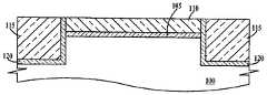
図1ないし図6は、本発明の実施例によるフィンFETの初期の製造ステップを示す断面図である。図1では、バルク・シリコン基板100上に形成されるのがパッド酸化シリコン層105であり、そのパッド酸化シリコン層105上に形成されるのがパッド窒化シリコン層110である。バルク・シリコン基板100が単結晶シリコンのモノリシック・ブロックとして画成される。パッド酸化シリコン層105およびパッド窒化シリコン層110を横断するように形成されるのが誘電体STI(シャロー・トレンチ・アイソレーション)115である。STI115の両側および底部に設けられるが上面には設けられない任意選択の誘電体のライナー120が図示される。パッド酸化シリコン層105およびパッド窒化シリコン層110中に開孔をフォトリソグラフィ技術で画成し、パッド層105、110によって保護されていないバルク・シリコン基板100中にトレンチを(例えば、反応性イオン・エッチング(RIE)によって)エッチング(食刻)し、そのトレンチを誘電体で以ってバックフィル(埋め戻し)し、STIの上面がパッド酸化シリコン層105の上面と同一平面になるように化学的物理的研磨(CMP)を行うことによってSTI115を形成することができる。1 to 6 are cross-sectional views showing initial manufacturing steps of a fin FET according to an embodiment of the present invention. In FIG. 1, a pad
一実施例では、パッド酸化シリコン層105はバルク・シリコン基板100の熱酸化により形成され、約5nmないし約20nmの厚さとする。一実施例では、パッド窒化シリコン層110は化学的気相蒸着(CVD)により形成され、約50nmないし約500nmの厚さとする。一実施例では、STI115はテトラエトキシシラン(TEOS)や高密度プラズマ(HDP)酸化物のようなCVD酸化物である。一実施例では、ライナー120は50nm未満の酸化シリコン、窒化シリコン、あるいは窒化シリコン下の酸化シリコンの二重層である。一実施例ではSTI115は約50nmおよび約500nmの間の厚さである。パッド窒化シリコン層110が選択的に酸化するために除去され、STI115がパッド酸化シリコン層105の上面とほぼ同一平面になるように平坦化される。In one embodiment, pad
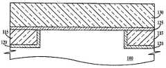
図2では、エッチング・ストップ層125がSTI115およびもし存在するときのライナー120の露出したエッジ(端部)の上方に付着される。そしてマンドレル層130がそのエッチング・ストップ層125の上方に付着される。一例では、エッチング・ストップ層125はCVD酸化シリコンを含み、その厚さが約2nmないし約10nmである。一例では、マンドレル層130は上述したCVD酸化物であり、その厚さが約100nmないし約500nmである。マンドレル層130の厚さが、その後形成されるシリコンのフィン(ひれ)の高さ(現在のバルク・シリコン基板100とエッチング・ストップ層125との界面から上方)を決める。In FIG. 2, an
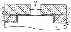
図3では、トレンチ135がマンドレル層130およびエッチング・ストップ層125を貫通するようにエッチングされ、トレンチ135の底部のバルク・シリコン基板100を露出する。一例では、トレンチ135の幅「W」が約20nmないし約100nmである。幅「W」は、その後形成されるシリコンのフィン(その後、側壁に酸化物があればそれよりも狭い)の幅を画成(規定)する。In FIG. 3, the
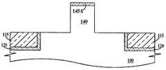
図4では、キャップ145で覆われる単結晶シリコンのフィン140がトレンチ135の中に形成される。フィン140はマンドレル層130の上面の上方まで選択的エピタキシャル成長によって形成してもよく、その後平坦化および凹部RIE(反応性イオン・エッチング)を施してもよい。一例では、フィン140の上部はマンドレル層130の上面から下方に約20nmから約100nmの間凹ませられる。一例では、キャップ145が、その凹みを覆うだけの十分な厚さの窒化シリコンのCVD付着(化学的蒸着)により形成されてキャップ145の上面がマンドレル層130の上面と同一面になるようにし、その後CMPを施してもよい。代替例では、ポリシリコンのフィンが単結晶シリコンのフィンの代わりに形成されてもよい。In FIG. 4, a single
図5では、マンドレル130(図4参照)が除去される。一例では、マンドレル層130が酸化物であり、キャップ145およびエッチング・ストップ層125が窒化シリコンであるとき、窒化シリコンより早く酸化物をエッチングするように選択的に作用するRIEで以ってマンドレルが除去される。代替例として、マンドレル層130がウエット・エッチング・プロセス(すなわち、マンドレル層130が酸化シリコンであるときフッ化水素酸水溶液)によって除去されてもよい。それから酸化シリコンよりも早く窒化シリコンをエッチングするように選択的に作用するRIEで以ってエッチング・ストップ層125が除去され、キャップ145(図4)は薄くなってキャップ145Aとなる。In FIG. 5, the mandrel 130 (see FIG. 4) is removed. In one example, when the
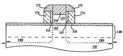
図6では、ゲート誘電体層150がフィン140の側壁に形成される。この現在の例では、ゲート誘電体層150が熱成長する酸化シリコンであり、従って露出したバルク・シリコン基板100の薄い領域もまた酸化される。代替例として、ゲート誘電体層150が付着(蒸着)されてもよい。付着されるゲート誘電体層150の例は、K(絶縁定数)の高い材料であってよい。その例として、以下に限定されるものではないが、Ta2O5、BaTiO3、HfO2、ZrO2、Al2O3などの金属酸化物、またはHfSixOy、HfSixOyNzなどの金属シリケート、或いはそれらの層を組み合わせたものを含んでいてもよい。Kの高い絶縁材料は約10よりも上の相対誘電率を有する。一例では、ゲート誘電体層150の厚さが約0.5nmと約20nmの間である。In FIG. 6, a gate
次に、ゲート155がフィン140を跨ぐように形成され、キャッピング層160がその上に形成されるがゲート155の側壁には形成されない(図7参照)。一例では、ゲート155は、ドープされたポリシリコン、もしくはドープされないポリシリコン、または高濃度のシリサイド(ケイ化物)を有する金属シリサイドの層を含み、フィン140の側壁を覆うに足るだけの厚さである。一例では、キャッピング層160が窒化シリコンであり、約100nmおよび約500nmの間の厚さである。Next, the
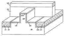
図7は図6に示す構造の3次元等角図である。図7では、ゲート155およびキャッピング層145Aがフィン140を横切る。一例では、フィン140およびゲート155が互いに直交する。一例では、フィン140およびゲート155がフィンの結晶面により定義される角度で交叉してもよい。一例では、ゲート155およびキャッピング層160が、ゲートのブランケットCVD付着、次いでCMP、次いでキャッピング層のブランケットCVD付着、次いでそのゲートおよびキャッピング層を画成するためのフォトリソグラフィック・プロセスおよびエッチング・プロセスにより形成される。FIG. 7 is a three-dimensional isometric view of the structure shown in FIG. In FIG. 7,
図8は図7に示した構造にその後の製造ステップを加えた構造の3次元等角図である。図8では、ソース/ドレイン180がイオン注入により形成され、それから第1の保護層165がフィン140およびゲート155の露出した側壁上に形成され、第2の保護層170がゲート155の側壁上の第1の保護層165の上方に形成され、そしてスペーサ175が第1および第2の保護層165および170の上部エッジ(上端)にキャッピング層160に隣接して形成される。第1および第2の保護層165および170ならびにスペーサ175を形成するには、その一例として以下のことを行う。
(1)第1の保護層165であるブランケット層を形成するために窒化シリコンのブランケットCVD付着を行い、
(2)第1の保護層165であるブランケット層の上方に第2の保護層170であるブランケット層を形成するためにCVD酸化物(前述)のブランケット付着を行い、
(3)キャッピング層160を露出するためにCVD酸化物のCMPを行い、
(4)キャッピング層160の上面の下方のCVD酸化物を凹ませるようにRIE凹部エッチングを行い、
(5)スペーサ175を形成するためにブランケットCVD窒化シリコン付着を行い、次いでスペーサRIEを行い、そして
(6)スペーサ175によって保護されない全てのCVD酸化物を除去するためにRIEを行う。FIG. 8 is a three-dimensional isometric view of the structure shown in FIG. 7 with subsequent manufacturing steps added. In FIG. 8, source /
(1) Perform blanket CVD deposition of silicon nitride to form a blanket layer which is the first
(2) In order to form a blanket layer that is the second
(3) CMP of CVD oxide to expose the
(4) RIE recess etching is performed so that the CVD oxide below the upper surface of the
(5) Perform blanket CVD silicon nitride deposition to form
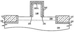
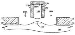
図9は図8の構造の上面図であり、図10、図11、図12および図13は図8に示す構造の、図9上の線10−10、線11−11、線12−12および線13−13に沿う断面図である。図11、図12および図13では、ソース/ドレイン180の境界を小破線で示していることに留意されたい。図10および図13では、バルク・シリコン基板100とフィン140の界面を大破線で示しているが、この界面はフィンがエピタキシャル成長されたので検出することができず、参照目的で示している。また図10および図13では、チャネル領域185がフィン140中の、ゲート155の下方にある。FIG. 9 is a top view of the structure of FIG. 8, and FIGS. 10, 11, 12, and 13 are lines 10-10, 11-11, and 12-12 on the structure of FIG. And FIG. 13 is a cross-sectional view taken along line 13-13. Note that in FIGS. 11, 12 and 13, the boundaries of the source /
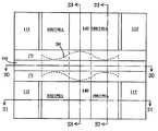
図14は図9の構造に追加処理した後の構造の上面図であり、図15、図16、図17および図18は夫々、図10、図11、図12および図13に示す構造に追加処理した後の構造の、図14上の線15−15、線16−16、線17−17および線18−18に沿う断面図である。図15および図18は夫々図10および図13と同一である。図14、図16および図17では、トレンチ190がバルク・シリコン基板100中に深さ「D」だけエッチングされているが、これはバルク・シリコン基板100が露出されている場合に酸化シリコンおよび窒化シリコンよりも早くシリコンをエッチングするように選択的に作用するRIEを用いるなどして得られる(図9、図11および図12参照)。一例で、「D」は約50nmないし約250nmである。一例で、「D」はSTI115の厚さ(或いはもしライナー120が存在するならSTI115およびライナー120の厚さ)の約半分である。フィン140はキャッピング層145A、ゲート誘電体層150および第1の保護層165によってエッチングから保護され、一方でゲート155は第1および第2の保護層165および170ならびにキャッピング層160およびスペーサ175によってエッチングから保護される。14 is a top view of the structure after addition processing to the structure of FIG. 9, and FIGS. 15, 16, 17, and 18 are added to the structures shown in FIGS. 10, 11, 12, and 13, respectively. FIG. 17 is a cross-sectional view of the structure after processing, taken along line 15-15, line 16-16, line 17-17, and line 18-18 on FIG. 15 and 18 are the same as FIGS. 10 and 13, respectively. In FIGS. 14, 16 and 17, the
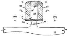
図19は図14の構造に追加処理した後の構造の上面図であり、図20、図21、図22および図23は夫々、図15、図16、図17および図18に示す構造に追加処理した後の構造の、図19上の線20−20、線21−21、線22−22および線23−23に沿う断面図である。図20は図15と同一である。図19、図21、図22および図23では、シリコンのウエット・エッチングが行われてきて、トレンチ190(図16および図17参照)を拡張し、トレンチ190Aを形成するとともにソース/ドレイン180中のフィン140をアンダーカットし、シリコンのぺデスタル195を残す。このぺデスタル195がフィン140をバルク・シリコン基板100にチャネル領域185で結合する。ぺデスタル195は図19に破線で示すエッジ200を有する。アンダーカットの量に依って、ソース/ドレイン180は完全にまたは部分的にアンダーカットされ、ぺデスタル195の断面積が変化する。チャネル領域185はアンダーカットされてもされなくてもよい。一例として、チャネル領域185が部分的にアンダーカットされ、ソース/ドレイン(図23には図示せず)が完全にアンダーカットされて、図23には存在しない。バルク・シリコン基板100の一部およびフィン140がアンダーカット・プロセスで除去される。このアンダーカットは、例えば硝酸およびフッ化水素酸の混合物中でウエット・エッチングすることによって、またはCF4またはSF4を用いるRIEによって等方性で行われてもよい。代替例では、アンダーカットが異方性で行われてもよい。これはシリコンの[001]結晶面を[001]結晶面よりも早くエッチングする水酸化カリウムまたは水酸化テトラメチルアンモニウムなど強い塩基の水溶液またはアルコール溶液でウエット・エッチングすることによって行われる。ぺデスタル195はチャネル領域185とバルク・シリコン基板100の間の導電性ボディ・コンタクトを提供し、浮遊ボディ効果をなくすことができる。FIG. 19 is a top view of the structure after addition processing to the structure of FIG. 14, and FIGS. 20, 21, 22, and 23 are added to the structures shown in FIGS. 15, 16, 17, and 18, respectively. FIG. 20 is a cross-sectional view of the structure after processing, taken along line 20-20, line 21-21, line 22-22, and line 23-23 on FIG. FIG. 20 is the same as FIG. 19, 21, 22 and 23, wet etching of silicon has been performed to expand trench 190 (see FIGS. 16 and 17) to form
図24は図19の構造に追加処理した後の構造の上面図であり、図25、図26、図27および図28は夫々、図20、図21、図22および図23に示す構造に追加処理した後の構造の、図24上の線25−25、線26−26、線27−27および線28−28に沿う断面図である。図24、図25、図26、図27および図28では、誘電体層205が付着され、トレンチ190Aのアンダーカット領域の充填(図示)または部分充填(図示せず)を行う。誘電体層205の上面はキャッピング層160の上面と同一平面上にある。一実施例では、誘電体層205はコンフォーマルなCVD酸化付着(TEOSまたはHDPなど)とそれに続くCMPにより形成される。アンダーカット領域190Aを完全に充填せず、ボイド(空隙)を残していてもよい。誘電体層205の残りがそのようなボイドを封止するからである。ソース/ドレイン180の下方のフィン140とバルク・シリコン基板100との間の距離「T」(図28参照)は、完全に充填されていようがボイドを含んでいようが、フィン140およびバルク・シリコン基板100間の寄生容量を大きく減じる。一実施例で「T」は、約50nmおよび約250nmの間である。24 is a top view of the structure after the addition processing to the structure of FIG. 19, and FIGS. 25, 26, 27, and 28 are added to the structures shown in FIGS. 20, 21, 22, and 23, respectively. FIG. 25 is a cross-sectional view of the structure after processing, taken along lines 25-25, 26-26, 27-27, and 28-28 on FIG. In FIGS. 24, 25, 26, 27, and 28, a
誘電体層205、キャッピング層145Aおよび160、ソース/ドレイン180およびゲート155まで貫通するコンタクト・バイア・ホールを形成することによって、(図示しないが従来よく知られている)接点即ちコンタクトがフィンFETに形成されても良い。次に、ワイヤリングのレベルを形成し、そして誘電体層を介在させるといった標準的な処理が行われて、本発明の実施例によるフィンFETデバイスを含む集積回路チップが完成される。By forming contact via holes that penetrate to the
このように、本発明の実施例は、浮遊ボディ効果なしに寄生容量を減じたフィンFETデバイスおよびその製造方法を提供する。Thus, embodiments of the present invention provide a finFET device with reduced parasitic capacitance without a floating body effect and a method of manufacturing the same.
以上のとおり、本発明を理解するために本発明の実施例を説明してきた。本発明が個別に記載した特定の実施例に限定されないこと、そして本発明の範囲から逸脱することなく種々の変形例、再構成例、代替例が可能であることは当業者に明らかであろう。特許請求の範囲が本発明の真の趣旨および範囲内にあるようなそのような全ての変形や変更を包含することを意図している。As described above, the embodiments of the present invention have been described in order to understand the present invention. It will be apparent to those skilled in the art that the present invention is not limited to the specific embodiments described individually and that various modifications, reconfigurations, and alternatives are possible without departing from the scope of the invention. . It is intended that the appended claims cover all such variations and modifications as fall within the true spirit and scope of this invention.
100 バルク・シリコン基板
105 パッド酸化シリコン層
110 パッド窒化シリコン層
115 STI
120 ライナー
125 エッチング・ストップ層
130 マンドレル層
135 トレンチ
140 フィン
145 キャップ
145A キャッピング層
150 ゲート誘電体層
155 ゲート
160 キャッピング層
165 第1の保護層
170 第2の保護層
175 スペーサ
180 ソース/ドレイン
185 チャネル領域
190 トレンチ
190A トレンチ
195 ペデスタル
200 エッジ
205 誘電体100
120
Claims (9)
Translated fromJapanese前記シリコン・ボディと前記バルク・シリコン基板との間のボディ・コンタクトと、
前記シリコン・ボディ中に形成され、かつ前記フィンFETの下方の誘電体層によって前記バルク・シリコン基板から絶縁された第1および第2のソース/ドレインと
を含む構造。A fin FET (field effect transistor) having a silicon body formed on a bulk silicon substrate;
A body contact between the silicon body and the bulk silicon substrate;
A structure comprising first and second sources / drains formed in the silicon body and insulated from the bulk silicon substrate by a dielectric layer below the finFET.
請求項1に記載の構造。The body contact includes a pedestal of the bulk silicon substrate that contacts the channel region of the fin FET between the first and second sources / drains and below the gate electrode of the fin FET. The structure of claim 1.
前記バルク・シリコン基板の前記上面に平行で前記第1の方向とは異なる第2の方向に延び、かつ前記チャネル領域の上方で交叉する導電性のゲート電極と、
前記ゲート電極および前記フィン間のゲート誘電体と、
前記バルク・シリコン基板と直接に物理的および電気的にコンタクトする、前記フィンの前記チャネル領域の少なくとも一部と、
前記第1のソース/ドレインの少なくとも一部と前記バルク・シリコン基板との間、および前記第2のソース/ドレインの少なくとも一部と前記バルク・シリコン基板との間の誘電体層と
を含む構造。A single crystal silicon fin extending in a first direction parallel to the top surface of the bulk silicon substrate, the fin having a channel region between the first and second source / drain;
A conductive gate electrode extending in a second direction different from the first direction parallel to the top surface of the bulk silicon substrate and intersecting above the channel region;
A gate dielectric between the gate electrode and the fin;
At least a portion of the channel region of the fin in direct physical and electrical contact with the bulk silicon substrate;
A structure including at least a portion of the first source / drain and the bulk silicon substrate and a dielectric layer between at least a portion of the second source / drain and the bulk silicon substrate. .
請求項3に記載の構造。Further including voids in the dielectric layer;
The structure of claim 3.
前記フィンの両側の側壁にゲート誘電体層を形成するステップと、
前記フィンのチャネル領域の上方のゲート電極であって、前記ゲート電極が前記フィンの前記両側の側壁上の前記ゲート誘電体層と直接に物理的にコンタクトするような前記ゲート電極を形成するステップと、
前記チャネル領域の第1の側の前記フィン中に第1のソース/ドレインを形成し、かつ前記チャネル領域の第2の側の前記フィン中に第2のソース/ドレインを形成するステップと、
ボイドを生じるために、前記第1および第2のソース/ドレインの少なくとも一部の下方から前記バルク・シリコン基板の一部を除去するステップと、
前記ボイドを誘電体材料で以って充填するステップと
を含む方法。Forming silicon fins on the top surface of the bulk silicon substrate;
Forming a gate dielectric layer on sidewalls on both sides of the fin;
Forming a gate electrode above the channel region of the fin, wherein the gate electrode is in direct physical contact with the gate dielectric layer on the sidewalls on both sides of the fin; ,
Forming a first source / drain in the fin on the first side of the channel region and forming a second source / drain in the fin on the second side of the channel region;
Removing a portion of the bulk silicon substrate from below at least a portion of the first and second source / drains to create voids;
Filling the void with a dielectric material.
前記フィンの両側の前記バルク・シリコン基板の中ではあるが、前記ゲート電極の下方ではないところにトレンチを形成するように第1のエッチングを行うステップと、
前記トレンチの両側を横方向にエッチングすることによって前記フィンをアンダーカットするように第2のエッチングを行うステップと
を含む、請求項5に記載の方法。Removing the portion of the bulk silicon substrate comprising:
Performing a first etch to form a trench in the bulk silicon substrate on both sides of the fin, but not under the gate electrode;
Performing a second etch to undercut the fin by laterally etching both sides of the trench.
請求項6に記載の方法。The second etch removes a layer from the bottom surface of the fin in a region of the fin exposed by the second etch;
The method of claim 6.
前記バルク・シリコン基板の前記上面にマンドレル層を形成するステップと、
前記バルク・シリコン基板の上面がトレンチの上部で露出された状態で、前記マンドレル層の中に前記トレンチをエッチングするステップと、
前記トレンチをシリコンで以って充填するステップと
を含む、請求項5に記載の方法。Forming the silicon fin comprises:
Forming a mandrel layer on the top surface of the bulk silicon substrate;
Etching the trench into the mandrel layer with the top surface of the bulk silicon substrate exposed at the top of the trench;
Filling the trench with silicon.
請求項5に記載の方法。The void extends below a portion of the channel region;
The method of claim 5.
Applications Claiming Priority (2)
| Application Number | Priority Date | Filing Date | Title |
|---|---|---|---|
| US11/427,486US7517764B2 (en) | 2006-06-29 | 2006-06-29 | Bulk FinFET device |
| US11/427,486 | 2006-06-29 |
Related Child Applications (1)
| Application Number | Title | Priority Date | Filing Date |
|---|---|---|---|
| JP2013025314ADivisionJP5648933B2 (en) | 2006-06-29 | 2013-02-13 | FinFET device structure and manufacturing method thereof |
Publications (2)
| Publication Number | Publication Date |
|---|---|
| JP2008010876Atrue JP2008010876A (en) | 2008-01-17 |
| JP5259990B2 JP5259990B2 (en) | 2013-08-07 |
Family
ID=38875688
Family Applications (2)
| Application Number | Title | Priority Date | Filing Date |
|---|---|---|---|
| JP2007168478AExpired - Fee RelatedJP5259990B2 (en) | 2006-06-29 | 2007-06-27 | FinFET device structure and manufacturing method thereof |
| JP2013025314AActiveJP5648933B2 (en) | 2006-06-29 | 2013-02-13 | FinFET device structure and manufacturing method thereof |
Family Applications After (1)
| Application Number | Title | Priority Date | Filing Date |
|---|---|---|---|
| JP2013025314AActiveJP5648933B2 (en) | 2006-06-29 | 2013-02-13 | FinFET device structure and manufacturing method thereof |
Country Status (4)
| Country | Link |
|---|---|
| US (4) | US7517764B2 (en) |
| JP (2) | JP5259990B2 (en) |
| CN (1) | CN101097956B (en) |
| TW (1) | TWI399856B (en) |
Cited By (3)
| Publication number | Priority date | Publication date | Assignee | Title |
|---|---|---|---|---|
| KR20210053169A (en)* | 2019-10-31 | 2021-05-11 | 타이완 세미콘덕터 매뉴팩쳐링 컴퍼니 리미티드 | Non-conformal capping layer and method forming same |
| EP4199108A1 (en) | 2021-12-14 | 2023-06-21 | United Semiconductor Japan Co., Ltd. | Semiconductor device and method of manufacturing semiconductor device |
| US12046660B2 (en) | 2019-10-31 | 2024-07-23 | Taiwan Semiconductor Manufacturing Company, Ltd. | Non-conformal capping layer and method forming same |
Families Citing this family (109)
| Publication number | Priority date | Publication date | Assignee | Title |
|---|---|---|---|---|
| US7384838B2 (en)* | 2005-09-13 | 2008-06-10 | International Business Machines Corporation | Semiconductor FinFET structures with encapsulated gate electrodes and methods for forming such semiconductor FinFET structures |
| US7510939B2 (en)* | 2006-01-31 | 2009-03-31 | International Business Machines Corporation | Microelectronic structure by selective deposition |
| US7663185B2 (en)* | 2006-05-27 | 2010-02-16 | Taiwan Semiconductor Manufacturing Co, Ltd | FIN-FET device structure formed employing bulk semiconductor substrate |
| US7517764B2 (en)* | 2006-06-29 | 2009-04-14 | International Business Machines Corporation | Bulk FinFET device |
| US7648915B2 (en)* | 2007-01-12 | 2010-01-19 | Micron Technology, Inc. | Methods of forming semiconductor constructions, and methods of recessing materials within openings |
| US8980756B2 (en) | 2007-07-30 | 2015-03-17 | Micron Technology, Inc. | Methods for device fabrication using pitch reduction |
| US8012839B2 (en) | 2008-02-29 | 2011-09-06 | Chartered Semiconductor Manufacturing, Ltd. | Method for fabricating a semiconductor device having an epitaxial channel and transistor having same |
| DE102008030864B4 (en)* | 2008-06-30 | 2010-06-17 | Advanced Micro Devices, Inc., Sunnyvale | Semiconductor device as a double-gate and tri-gate transistor, which are constructed on a solid substrate and method for producing the transistor |
| KR101168468B1 (en)* | 2008-07-14 | 2012-07-26 | 에스케이하이닉스 주식회사 | Method for fabricating semiconductor device |
| US8153493B2 (en)* | 2008-08-28 | 2012-04-10 | Taiwan Semiconductor Manufacturing Company, Ltd. | FinFET process compatible native transistor |
| US8227867B2 (en)* | 2008-12-23 | 2012-07-24 | International Business Machines Corporation | Body contacted hybrid surface semiconductor-on-insulator devices |
| US7871873B2 (en)* | 2009-03-27 | 2011-01-18 | Global Foundries Inc. | Method of forming fin structures using a sacrificial etch stop layer on bulk semiconductor material |
| US8124507B2 (en)* | 2009-06-24 | 2012-02-28 | Panasonic Corporation | Semiconductor device and method for fabricating the same |
| CN101995713B (en)* | 2009-08-21 | 2012-08-01 | 北京京东方光电科技有限公司 | TFT-LCD array substrate and manufacturing method thereof |
| JP2011066362A (en)* | 2009-09-18 | 2011-03-31 | Toshiba Corp | Semiconductor device |
| US8946028B2 (en)* | 2009-10-06 | 2015-02-03 | International Business Machines Corporation | Merged FinFETs and method of manufacturing the same |
| US8101486B2 (en) | 2009-10-07 | 2012-01-24 | Globalfoundries Inc. | Methods for forming isolated fin structures on bulk semiconductor material |
| US8445340B2 (en)* | 2009-11-19 | 2013-05-21 | Taiwan Semiconductor Manufacturing Company, Ltd. | Sacrificial offset protection film for a FinFET device |
| CN102117829B (en)* | 2009-12-30 | 2012-11-21 | 中国科学院微电子研究所 | Fin type transistor structure and manufacturing method thereof |
| US8362572B2 (en)* | 2010-02-09 | 2013-01-29 | Taiwan Semiconductor Manufacturing Co., Ltd. | Lower parasitic capacitance FinFET |
| CN102157554A (en)* | 2010-02-12 | 2011-08-17 | 中国科学院微电子研究所 | Fin transistor structure and fabrication method thereof |
| US8174055B2 (en)* | 2010-02-17 | 2012-05-08 | Globalfoundries Inc. | Formation of FinFET gate spacer |
| US8263451B2 (en) | 2010-02-26 | 2012-09-11 | Taiwan Semiconductor Manufacturing Company, Ltd. | Epitaxy profile engineering for FinFETs |
| US9312179B2 (en)* | 2010-03-17 | 2016-04-12 | Taiwan-Semiconductor Manufacturing Co., Ltd. | Method of making a finFET, and finFET formed by the method |
| CN101986435B (en)* | 2010-06-25 | 2012-12-19 | 中国科学院上海微系统与信息技术研究所 | Manufacturing method of metal oxide semiconductor (MOS) device structure for preventing floating body and self-heating effect |
| WO2012015022A1 (en)* | 2010-07-30 | 2012-02-02 | 京セラ株式会社 | Composite substrate, electronic component, method for producing composite substrate, and method for manufacturing electronic component |
| CN102456734B (en)* | 2010-10-29 | 2015-06-10 | 中国科学院微电子研究所 | Semiconductor structure and manufacturing method thereof |
| CN102569074B (en)* | 2010-12-08 | 2014-07-02 | 中国科学院微电子研究所 | Preparation method of gate-all-around field effect transistor |
| US9240350B2 (en)* | 2011-05-16 | 2016-01-19 | Varian Semiconductor Equipment Associates, Inc. | Techniques for forming 3D structures |
| US8597994B2 (en) | 2011-05-23 | 2013-12-03 | GlobalFoundries, Inc. | Semiconductor device and method of fabrication |
| JP5325932B2 (en)* | 2011-05-27 | 2013-10-23 | 株式会社東芝 | Semiconductor device and manufacturing method thereof |
| CN102842595B (en)* | 2011-06-20 | 2015-12-02 | 中国科学院微电子研究所 | Semiconductor device and method for manufacturing the same |
| US8643108B2 (en) | 2011-08-19 | 2014-02-04 | Altera Corporation | Buffered finFET device |
| US9637810B2 (en) | 2011-09-30 | 2017-05-02 | Intel Corporation | Tungsten gates for non-planar transistors |
| US9202699B2 (en) | 2011-09-30 | 2015-12-01 | Intel Corporation | Capping dielectric structure for transistor gates |
| EP2761662B1 (en) | 2011-09-30 | 2022-02-02 | Sony Group Corporation | Tungsten gates for non-planar transistors |
| CN103918083A (en) | 2011-10-01 | 2014-07-09 | 英特尔公司 | Source/drain contacts for non-planar transistors |
| US9087915B2 (en) | 2011-12-06 | 2015-07-21 | Intel Corporation | Interlayer dielectric for non-planar transistors |
| CN103165428B (en)* | 2011-12-14 | 2015-12-09 | 中芯国际集成电路制造(上海)有限公司 | Make the method for semiconductor device |
| DE112011105979B4 (en) | 2011-12-20 | 2022-09-15 | Intel Corporation | Semiconductor device with isolated semiconductor body parts and manufacturing method |
| CN103177963B (en)* | 2011-12-21 | 2016-02-17 | 中芯国际集成电路制造(上海)有限公司 | A kind of manufacture method of FinFET |
| US9117877B2 (en) | 2012-01-16 | 2015-08-25 | Globalfoundries Inc. | Methods of forming a dielectric cap layer on a metal gate structure |
| US8659097B2 (en)* | 2012-01-16 | 2014-02-25 | Taiwan Semiconductor Manufacturing Company, Ltd. | Control fin heights in FinFET structures |
| US8466012B1 (en) | 2012-02-01 | 2013-06-18 | International Business Machines Corporation | Bulk FinFET and SOI FinFET hybrid technology |
| CN103311111B (en)* | 2012-03-16 | 2015-12-16 | 中芯国际集成电路制造(上海)有限公司 | The formation method of fin transistor |
| CN103367147A (en)* | 2012-03-29 | 2013-10-23 | 中芯国际集成电路制造(上海)有限公司 | Manufacturing method of fin type semiconductor device |
| CN103378005B (en)* | 2012-04-23 | 2016-04-20 | 中芯国际集成电路制造(上海)有限公司 | The manufacture method of multiple gate field effect transistor fin structure |
| US8853750B2 (en) | 2012-04-27 | 2014-10-07 | International Business Machines Corporation | FinFET with enhanced embedded stressor |
| US8921218B2 (en) | 2012-05-18 | 2014-12-30 | Taiwan Semiconductor Manufacturing Company, Ltd. | Metal gate finFET device and method of fabricating thereof |
| US8470714B1 (en)* | 2012-05-22 | 2013-06-25 | United Microelectronics Corp. | Method of forming fin structures in integrated circuits |
| CN102683418B (en)* | 2012-05-22 | 2014-11-26 | 清华大学 | FINFET dynamic random access memory unit and processing method thereof |
| CN103515234B (en)* | 2012-06-25 | 2016-12-21 | 中芯国际集成电路制造(上海)有限公司 | The method forming FinFET |
| US9018713B2 (en) | 2012-06-25 | 2015-04-28 | International Business Machines Corporation | Plural differential pair employing FinFET structure |
| US9024387B2 (en) | 2012-06-25 | 2015-05-05 | International Business Machines Corporation | FinFET with body contact |
| US9142400B1 (en) | 2012-07-17 | 2015-09-22 | Stc.Unm | Method of making a heteroepitaxial layer on a seed area |
| US8741701B2 (en) | 2012-08-14 | 2014-06-03 | International Business Machines Corporation | Fin structure formation including partial spacer removal |
| US8993402B2 (en)* | 2012-08-16 | 2015-03-31 | International Business Machines Corporation | Method of manufacturing a body-contacted SOI FINFET |
| CN103594497A (en)* | 2012-08-16 | 2014-02-19 | 中国科学院微电子研究所 | Semiconductor device and method for manufacturing the same |
| CN103681331B (en)* | 2012-09-10 | 2016-06-29 | 中芯国际集成电路制造(上海)有限公司 | Fin field effect pipe and forming method thereof |
| US9240352B2 (en) | 2012-10-24 | 2016-01-19 | Globalfoundries Inc. | Bulk finFET well contacts with fin pattern uniformity |
| US9263585B2 (en) | 2012-10-30 | 2016-02-16 | Globalfoundries Inc. | Methods of forming enhanced mobility channel regions on 3D semiconductor devices, and devices comprising same |
| US8697536B1 (en) | 2012-11-27 | 2014-04-15 | International Business Machines Corporation | Locally isolated protected bulk finfet semiconductor device |
| CN103855026B (en)* | 2012-12-06 | 2017-04-19 | 中国科学院微电子研究所 | Finfet and manufacturing method thereof |
| US9362406B2 (en)* | 2012-12-12 | 2016-06-07 | Taiwan Semiconductor Manufacturing Company Limited | Faceted finFET |
| US8716156B1 (en) | 2013-02-01 | 2014-05-06 | Globalfoundries Inc. | Methods of forming fins for a FinFET semiconductor device using a mandrel oxidation process |
| US8906759B2 (en)* | 2013-02-25 | 2014-12-09 | International Business Machines Corporation | Silicon nitride gate encapsulation by implantation |
| US8963258B2 (en) | 2013-03-13 | 2015-02-24 | Taiwan Semiconductor Manufacturing Company | FinFET with bottom SiGe layer in source/drain |
| US8940602B2 (en) | 2013-04-11 | 2015-01-27 | International Business Machines Corporation | Self-aligned structure for bulk FinFET |
| US8912609B2 (en) | 2013-05-08 | 2014-12-16 | International Business Machines Corporation | Low extension resistance III-V compound fin field effect transistor |
| US8816428B1 (en)* | 2013-05-30 | 2014-08-26 | International Business Machines Corporation | Multigate device isolation on bulk semiconductors |
| US20140374838A1 (en)* | 2013-06-21 | 2014-12-25 | Taiwan Semiconductor Manufacturing Company, Ltd. | FinFETs with Nitride Liners and Methods of Forming the Same |
| US9385233B2 (en) | 2013-06-26 | 2016-07-05 | Globalfoundries Inc. | Bulk finFET with partial dielectric isolation featuring a punch-through stopping layer under the oxide |
| CN104282571B (en)* | 2013-07-09 | 2016-12-28 | 中国科学院微电子研究所 | Fin-type field effect transistor and manufacturing method thereof |
| CN104425346A (en)* | 2013-09-10 | 2015-03-18 | 中国科学院微电子研究所 | Method for manufacturing fin on insulator |
| US9324841B2 (en) | 2013-10-09 | 2016-04-26 | Globalfoundries Inc. | Methods for preventing oxidation damage during FinFET fabrication |
| US9093561B2 (en)* | 2013-11-21 | 2015-07-28 | GlobalFoundries, Inc. | Modified, etch-resistant gate structure(s) facilitating circuit fabrication |
| KR102145262B1 (en)* | 2013-12-16 | 2020-08-18 | 인텔 코포레이션 | Dual strained cladding layers for semiconductor devices |
| US9224841B2 (en) | 2014-01-23 | 2015-12-29 | Globalfoundries Inc. | Semiconductor fins on a trench isolation region in a bulk semiconductor substrate and a method of forming the semiconductor fins |
| US20150214331A1 (en)* | 2014-01-30 | 2015-07-30 | Globalfoundries Inc. | Replacement metal gate including dielectric gate material |
| US9570554B2 (en)* | 2014-04-04 | 2017-02-14 | International Business Machines Corporation | Robust gate spacer for semiconductor devices |
| US9093478B1 (en) | 2014-04-11 | 2015-07-28 | International Business Machines Corporation | Integrated circuit structure with bulk silicon FinFET and methods of forming |
| TWI538108B (en)* | 2014-05-08 | 2016-06-11 | 林崇榮 | Non-volatile memory with resistive element and manufacturing method thereof |
| CN105097533B (en)* | 2014-05-12 | 2018-06-29 | 中芯国际集成电路制造(上海)有限公司 | The forming method of semiconductor structure |
| US9548358B2 (en) | 2014-05-19 | 2017-01-17 | International Business Machines Corporation | Dual fill silicon-on-nothing field effect transistor |
| US9312364B2 (en)* | 2014-05-27 | 2016-04-12 | International Business Machines Corporation | finFET with dielectric isolation after gate module for improved source and drain region epitaxial growth |
| US20150372107A1 (en)* | 2014-06-18 | 2015-12-24 | Stmicroelectronics, Inc. | Semiconductor devices having fins, and methods of forming semiconductor devices having fins |
| US10347766B2 (en)* | 2014-09-02 | 2019-07-09 | Taiwan Semiconductor Manufacturing Co., Ltd. | Semiconductor device and method of fabricating the same |
| KR102150942B1 (en) | 2014-12-01 | 2020-09-03 | 삼성전자주식회사 | Semiconductor device including fin FET |
| TWI682466B (en)* | 2015-01-28 | 2020-01-11 | 聯華電子股份有限公司 | Manufacturing method of an oxide layer, manufacturing method of a semiconductor structure using the same and semiconductor structure manufactured thereby |
| US9525036B2 (en) | 2015-03-19 | 2016-12-20 | Samsung Electronics Co., Ltd. | Semiconductor device having gate electrode with spacers on fin structure and silicide layer filling the recess |
| CN105633157B (en)* | 2015-03-31 | 2019-07-30 | 中国科学院微电子研究所 | Semiconductor device and method of manufacturing the same |
| CN106298522B (en)* | 2015-05-20 | 2019-11-05 | 中芯国际集成电路制造(上海)有限公司 | The forming method of semiconductor structure |
| US10084085B2 (en) | 2015-06-11 | 2018-09-25 | Taiwan Semiconductor Manufacturing Co., Ltd. | Fin field effect transistor (FinFET) device structure with stop layer and method for forming the same |
| US9564489B2 (en)* | 2015-06-29 | 2017-02-07 | Taiwan Semiconductor Manufacturing Company, Ltd. | Multiple gate field-effect transistors having oxygen-scavenged gate stack |
| CN104966669A (en)* | 2015-07-22 | 2015-10-07 | 上海华力微电子有限公司 | Totally-surrounding gate structure manufacturing method |
| CN106549053B (en) | 2015-09-17 | 2021-07-27 | 联华电子股份有限公司 | Semiconductor structure and method of making the same |
| US9779959B2 (en)* | 2015-09-17 | 2017-10-03 | Taiwan Semiconductor Manufacturing Co., Ltd. | Structure and formation method of semiconductor device structure |
| US10020304B2 (en)* | 2015-11-16 | 2018-07-10 | Taiwan Semiconductor Manufacturing Co., Ltd. | Fin field effect transistor, semiconductor device and fabricating method thereof |
| US9620360B1 (en)* | 2015-11-27 | 2017-04-11 | International Business Machines Corporation | Fabrication of semiconductor junctions |
| US10903372B2 (en)* | 2015-12-11 | 2021-01-26 | Intel Corporation | Metal-oxide-polysilicon tunable resistor for flexible circuit design and method of fabricating same |
| US10217707B2 (en)* | 2016-09-16 | 2019-02-26 | International Business Machines Corporation | Trench contact resistance reduction |
| US9773893B1 (en) | 2016-09-26 | 2017-09-26 | International Business Machines Corporation | Forming a sacrificial liner for dual channel devices |
| KR102575366B1 (en) | 2016-11-09 | 2023-09-05 | 삼성전자주식회사 | Semiconductor device and method for fabricating the same |
| US9972621B1 (en)* | 2017-04-10 | 2018-05-15 | Globalfoundries Inc. | Fin structure in sublitho dimension for high performance CMOS application |
| US10629730B2 (en)* | 2018-05-25 | 2020-04-21 | International Business Machines Corporation | Body contact in Fin field effect transistor design |
| US10461154B1 (en)* | 2018-06-21 | 2019-10-29 | International Business Machines Corporation | Bottom isolation for nanosheet transistors on bulk substrate |
| KR102516879B1 (en) | 2018-08-17 | 2023-03-31 | 삼성전자주식회사 | Semiconductor devices with various line widths and method for manufacturing the same |
| US10896971B2 (en)* | 2019-02-25 | 2021-01-19 | International Business Machines Corporation | Vertical transistor with body contact fabrication |
| CN112271216B (en)* | 2020-09-18 | 2023-04-07 | 宁波大学 | Three-input FinFET with series operation function |
Citations (7)
| Publication number | Priority date | Publication date | Assignee | Title |
|---|---|---|---|---|
| JPH04162727A (en)* | 1990-10-26 | 1992-06-08 | Fujitsu Ltd | Manufacturing method of semiconductor device |
| JPH05167043A (en)* | 1991-04-26 | 1993-07-02 | Canon Inc | Semiconductor device having improved insulated gate transistor |
| JPH10209264A (en)* | 1997-01-17 | 1998-08-07 | Sony Corp | Method for isolating element of semiconductor device, semiconductor device and its manufacturing method |
| JP2001148479A (en)* | 1999-10-12 | 2001-05-29 | Samsung Electronics Co Ltd | Semiconductor device having partial SOI structure and method of manufacturing the same |
| JP2004281782A (en)* | 2003-03-17 | 2004-10-07 | Toshiba Corp | Semiconductor device and manufacturing method thereof |
| JP2004336052A (en)* | 2003-05-02 | 2004-11-25 | Samsung Electronics Co Ltd | Semiconductor device and method of manufacturing the same |
| JP2005252268A (en)* | 2004-03-05 | 2005-09-15 | Samsung Electronics Co Ltd | Manufacturing method of semiconductor device including buried oxide film and semiconductor device including the same |
Family Cites Families (20)
| Publication number | Priority date | Publication date | Assignee | Title |
|---|---|---|---|---|
| JP2768719B2 (en)* | 1988-11-21 | 1998-06-25 | 株式会社日立製作所 | Semiconductor device and semiconductor storage device |
| US5384710A (en)* | 1990-03-13 | 1995-01-24 | National Semiconductor Corporation | Circuit level netlist generation |
| US6376286B1 (en)* | 1999-10-20 | 2002-04-23 | Advanced Micro Devices, Inc. | Field effect transistor with non-floating body and method for forming same on a bulk silicon wafer |
| US6662350B2 (en)* | 2002-01-28 | 2003-12-09 | International Business Machines Corporation | FinFET layout generation |
| US7335545B2 (en)* | 2002-06-07 | 2008-02-26 | Amberwave Systems Corporation | Control of strain in device layers by prevention of relaxation |
| EP1519420A2 (en)* | 2003-09-25 | 2005-03-30 | Interuniversitaire Microelectronica Centrum vzw ( IMEC) | Multiple gate semiconductor device and method for forming same |
| US6960804B1 (en)* | 2003-08-04 | 2005-11-01 | Hussman Corporation | Semiconductor device having a gate structure surrounding a fin |
| US7095065B2 (en)* | 2003-08-05 | 2006-08-22 | Advanced Micro Devices, Inc. | Varying carrier mobility in semiconductor devices to achieve overall design goals |
| US7388258B2 (en)* | 2003-12-10 | 2008-06-17 | International Business Machines Corporation | Sectional field effect devices |
| US7105390B2 (en)* | 2003-12-30 | 2006-09-12 | Intel Corporation | Nonplanar transistors with metal gate electrodes |
| US7268058B2 (en)* | 2004-01-16 | 2007-09-11 | Intel Corporation | Tri-gate transistors and methods to fabricate same |
| US6989308B2 (en)* | 2004-03-11 | 2006-01-24 | International Business Machines Corporation | Method of forming FinFET gates without long etches |
| KR100626372B1 (en)* | 2004-04-09 | 2006-09-20 | 삼성전자주식회사 | Semiconductor device having field effect transistor and manufacturing method thereof |
| US7101763B1 (en)* | 2005-05-17 | 2006-09-05 | International Business Machines Corporation | Low capacitance junction-isolation for bulk FinFET technology |
| US7279375B2 (en)* | 2005-06-30 | 2007-10-09 | Intel Corporation | Block contact architectures for nanoscale channel transistors |
| KR100849186B1 (en)* | 2006-04-28 | 2008-07-30 | 주식회사 하이닉스반도체 | Method for manufacturing semiconductor device using lsoi process |
| KR100764360B1 (en)* | 2006-04-28 | 2007-10-08 | 주식회사 하이닉스반도체 | Semiconductor device and manufacturing method thereof |
| US7422960B2 (en)* | 2006-05-17 | 2008-09-09 | Micron Technology, Inc. | Method of forming gate arrays on a partial SOI substrate |
| US7517764B2 (en)* | 2006-06-29 | 2009-04-14 | International Business Machines Corporation | Bulk FinFET device |
| US7485520B2 (en)* | 2007-07-05 | 2009-02-03 | International Business Machines Corporation | Method of manufacturing a body-contacted finfet |
- 2006
- 2006-06-29USUS11/427,486patent/US7517764B2/enactiveActive
- 2007
- 2007-04-16CNCN2007100965809Apatent/CN101097956B/enactiveActive
- 2007-06-15TWTW096121647Apatent/TWI399856B/ennot_activeIP Right Cessation
- 2007-06-27JPJP2007168478Apatent/JP5259990B2/ennot_activeExpired - Fee Related
- 2007-10-24USUS11/923,121patent/US20080042219A1/ennot_activeAbandoned
- 2008
- 2008-02-11USUS12/028,916patent/US7667248B2/enactiveActive
- 2008-06-05USUS12/133,440patent/US7863122B2/enactiveActive
- 2013
- 2013-02-13JPJP2013025314Apatent/JP5648933B2/enactiveActive
Patent Citations (7)
| Publication number | Priority date | Publication date | Assignee | Title |
|---|---|---|---|---|
| JPH04162727A (en)* | 1990-10-26 | 1992-06-08 | Fujitsu Ltd | Manufacturing method of semiconductor device |
| JPH05167043A (en)* | 1991-04-26 | 1993-07-02 | Canon Inc | Semiconductor device having improved insulated gate transistor |
| JPH10209264A (en)* | 1997-01-17 | 1998-08-07 | Sony Corp | Method for isolating element of semiconductor device, semiconductor device and its manufacturing method |
| JP2001148479A (en)* | 1999-10-12 | 2001-05-29 | Samsung Electronics Co Ltd | Semiconductor device having partial SOI structure and method of manufacturing the same |
| JP2004281782A (en)* | 2003-03-17 | 2004-10-07 | Toshiba Corp | Semiconductor device and manufacturing method thereof |
| JP2004336052A (en)* | 2003-05-02 | 2004-11-25 | Samsung Electronics Co Ltd | Semiconductor device and method of manufacturing the same |
| JP2005252268A (en)* | 2004-03-05 | 2005-09-15 | Samsung Electronics Co Ltd | Manufacturing method of semiconductor device including buried oxide film and semiconductor device including the same |
Cited By (5)
| Publication number | Priority date | Publication date | Assignee | Title |
|---|---|---|---|---|
| KR20210053169A (en)* | 2019-10-31 | 2021-05-11 | 타이완 세미콘덕터 매뉴팩쳐링 컴퍼니 리미티드 | Non-conformal capping layer and method forming same |
| KR102412763B1 (en)* | 2019-10-31 | 2022-06-27 | 타이완 세미콘덕터 매뉴팩쳐링 컴퍼니 리미티드 | Non-conformal capping layer and method forming same |
| US11437491B2 (en) | 2019-10-31 | 2022-09-06 | Taiwan Semiconductor Manufacturing Company, Ltd. | Non-conformal capping layer and method forming same |
| US12046660B2 (en) | 2019-10-31 | 2024-07-23 | Taiwan Semiconductor Manufacturing Company, Ltd. | Non-conformal capping layer and method forming same |
| EP4199108A1 (en) | 2021-12-14 | 2023-06-21 | United Semiconductor Japan Co., Ltd. | Semiconductor device and method of manufacturing semiconductor device |
Also Published As
| Publication number | Publication date |
|---|---|
| CN101097956B (en) | 2012-06-27 |
| JP5648933B2 (en) | 2015-01-07 |
| US7517764B2 (en) | 2009-04-14 |
| TWI399856B (en) | 2013-06-21 |
| US7863122B2 (en) | 2011-01-04 |
| US20080001187A1 (en) | 2008-01-03 |
| JP5259990B2 (en) | 2013-08-07 |
| US20080233699A1 (en) | 2008-09-25 |
| TW200807717A (en) | 2008-02-01 |
| US7667248B2 (en) | 2010-02-23 |
| JP2013123077A (en) | 2013-06-20 |
| US20080142891A1 (en) | 2008-06-19 |
| US20080042219A1 (en) | 2008-02-21 |
| CN101097956A (en) | 2008-01-02 |
Similar Documents
| Publication | Publication Date | Title |
|---|---|---|
| JP5648933B2 (en) | FinFET device structure and manufacturing method thereof | |
| KR102688159B1 (en) | A semiconductor device | |
| US7879659B2 (en) | Methods of fabricating semiconductor devices including dual fin structures | |
| KR100487567B1 (en) | Method for fabricating a finfet in a semiconductor device | |
| KR100584776B1 (en) | Active structure formation method, device isolation method and transistor formation method of semiconductor device | |
| TWI509736B (en) | Semiconductor structure and method of forming same | |
| KR101093931B1 (en) | A DDR circuit comprising a method of forming field effect transistors, a plurality of field effect transistors, and a plurality of individual memory cells | |
| US8859389B2 (en) | Methods of making fins and fin field effect transistors (FinFETs) | |
| KR20080099485A (en) | Transistor of semiconductor device and manufacturing method thereof | |
| KR20180007356A (en) | Semiconductor device | |
| JP2006049627A (en) | Semiconductor device and manufacturing method thereof | |
| US7833861B2 (en) | Semiconductor device having recess channel structure and method for manufacturing the same | |
| JP2009021503A (en) | Semiconductor device and manufacturing method thereof | |
| US7348641B2 (en) | Structure and method of making double-gated self-aligned finFET having gates of different lengths | |
| KR100618904B1 (en) | Semiconductor device including FIFNFT and manufacturing method | |
| KR20240137421A (en) | Integrated circuit device | |
| CN116072675A (en) | Semiconductor structure and forming method thereof | |
| US7250347B2 (en) | Double-gate FETs (Field Effect Transistors) | |
| KR20100078964A (en) | Semiconductor device and method of manufacturing the same | |
| KR20070101435A (en) | Semiconductor device and manufacturing method thereof | |
| CN116314028A (en) | Semiconductor structures and methods of forming them | |
| CN115036370A (en) | Semiconductor structure and method of forming the same | |
| JP2009252814A (en) | Method of manufacturing semiconductor device, and semiconductor device |
Legal Events
| Date | Code | Title | Description |
|---|---|---|---|
| A621 | Written request for application examination | Free format text:JAPANESE INTERMEDIATE CODE: A621 Effective date:20100323 | |
| A977 | Report on retrieval | Free format text:JAPANESE INTERMEDIATE CODE: A971007 Effective date:20121108 | |
| A131 | Notification of reasons for refusal | Free format text:JAPANESE INTERMEDIATE CODE: A131 Effective date:20121113 | |
| RD12 | Notification of acceptance of power of sub attorney | Free format text:JAPANESE INTERMEDIATE CODE: A7432 Effective date:20121127 | |
| A521 | Request for written amendment filed | Free format text:JAPANESE INTERMEDIATE CODE: A821 Effective date:20121127 | |
| A521 | Request for written amendment filed | Free format text:JAPANESE INTERMEDIATE CODE: A523 Effective date:20130213 | |
| TRDD | Decision of grant or rejection written | ||
| A01 | Written decision to grant a patent or to grant a registration (utility model) | Free format text:JAPANESE INTERMEDIATE CODE: A01 Effective date:20130409 | |
| RD14 | Notification of resignation of power of sub attorney | Free format text:JAPANESE INTERMEDIATE CODE: A7434 Effective date:20130409 | |
| A61 | First payment of annual fees (during grant procedure) | Free format text:JAPANESE INTERMEDIATE CODE: A61 Effective date:20130425 | |
| FPAY | Renewal fee payment (event date is renewal date of database) | Free format text:PAYMENT UNTIL: 20160502 Year of fee payment:3 | |
| R150 | Certificate of patent or registration of utility model | Ref document number:5259990 Country of ref document:JP Free format text:JAPANESE INTERMEDIATE CODE: R150 Free format text:JAPANESE INTERMEDIATE CODE: R150 | |
| LAPS | Cancellation because of no payment of annual fees |