JP2008010859A - Semiconductor device - Google Patents
Semiconductor deviceDownload PDFInfo
- Publication number
- JP2008010859A JP2008010859AJP2007147089AJP2007147089AJP2008010859AJP 2008010859 AJP2008010859 AJP 2008010859AJP 2007147089 AJP2007147089 AJP 2007147089AJP 2007147089 AJP2007147089 AJP 2007147089AJP 2008010859 AJP2008010859 AJP 2008010859A
- Authority
- JP
- Japan
- Prior art keywords
- wiring
- analog
- power supply
- wiring portion
- digital
- Prior art date
- Legal status (The legal status is an assumption and is not a legal conclusion. Google has not performed a legal analysis and makes no representation as to the accuracy of the status listed.)
- Pending
Links
- 239000004065semiconductorSubstances0.000titleclaimsabstractdescription243
- 239000000758substrateSubstances0.000claimsdescription108
- 239000003990capacitorSubstances0.000claimsdescription3
- 229910000679solderInorganic materials0.000description41
- 230000000903blocking effectEffects0.000description11
- 238000010586diagramMethods0.000description11
- 230000000694effectsEffects0.000description10
- 238000000034methodMethods0.000description8
- 230000004048modificationEffects0.000description8
- 238000012986modificationMethods0.000description8
- 239000002184metalSubstances0.000description7
- 239000004020conductorSubstances0.000description6
- 230000008878couplingEffects0.000description6
- 238000010168coupling processMethods0.000description6
- 238000005859coupling reactionMethods0.000description6
- 230000002829reductive effectEffects0.000description5
- 238000005516engineering processMethods0.000description3
- 238000007789sealingMethods0.000description3
- 230000000087stabilizing effectEffects0.000description3
- 230000005540biological transmissionEffects0.000description2
- 230000036961partial effectEffects0.000description2
- 230000008569processEffects0.000description2
- 239000011347resinSubstances0.000description2
- 229920005989resinPolymers0.000description2
- 230000002441reversible effectEffects0.000description2
- 230000008054signal transmissionEffects0.000description2
- 230000002238attenuated effectEffects0.000description1
- 239000002131composite materialSubstances0.000description1
- 238000011109contaminationMethods0.000description1
- 230000001771impaired effectEffects0.000description1
- 230000002452interceptive effectEffects0.000description1
- 239000000463materialSubstances0.000description1
- 230000007246mechanismEffects0.000description1
- 238000004806packaging method and processMethods0.000description1
- 230000002093peripheral effectEffects0.000description1
- 230000009467reductionEffects0.000description1
- 230000003252repetitive effectEffects0.000description1
Images


Classifications
- H—ELECTRICITY
- H01—ELECTRIC ELEMENTS
- H01L—SEMICONDUCTOR DEVICES NOT COVERED BY CLASS H10
- H01L2224/00—Indexing scheme for arrangements for connecting or disconnecting semiconductor or solid-state bodies and methods related thereto as covered by H01L24/00
- H01L2224/01—Means for bonding being attached to, or being formed on, the surface to be connected, e.g. chip-to-package, die-attach, "first-level" interconnects; Manufacturing methods related thereto
- H01L2224/10—Bump connectors; Manufacturing methods related thereto
- H01L2224/15—Structure, shape, material or disposition of the bump connectors after the connecting process
- H01L2224/16—Structure, shape, material or disposition of the bump connectors after the connecting process of an individual bump connector
- H01L2224/161—Disposition
- H01L2224/16151—Disposition the bump connector connecting between a semiconductor or solid-state body and an item not being a semiconductor or solid-state body, e.g. chip-to-substrate, chip-to-passive
- H01L2224/16221—Disposition the bump connector connecting between a semiconductor or solid-state body and an item not being a semiconductor or solid-state body, e.g. chip-to-substrate, chip-to-passive the body and the item being stacked
- H01L2224/16225—Disposition the bump connector connecting between a semiconductor or solid-state body and an item not being a semiconductor or solid-state body, e.g. chip-to-substrate, chip-to-passive the body and the item being stacked the item being non-metallic, e.g. insulating substrate with or without metallisation
- H—ELECTRICITY
- H01—ELECTRIC ELEMENTS
- H01L—SEMICONDUCTOR DEVICES NOT COVERED BY CLASS H10
- H01L2924/00—Indexing scheme for arrangements or methods for connecting or disconnecting semiconductor or solid-state bodies as covered by H01L24/00
- H01L2924/15—Details of package parts other than the semiconductor or other solid state devices to be connected
- H01L2924/151—Die mounting substrate
- H01L2924/153—Connection portion
- H01L2924/1531—Connection portion the connection portion being formed only on the surface of the substrate opposite to the die mounting surface
- H01L2924/15311—Connection portion the connection portion being formed only on the surface of the substrate opposite to the die mounting surface being a ball array, e.g. BGA
- H—ELECTRICITY
- H01—ELECTRIC ELEMENTS
- H01L—SEMICONDUCTOR DEVICES NOT COVERED BY CLASS H10
- H01L2924/00—Indexing scheme for arrangements or methods for connecting or disconnecting semiconductor or solid-state bodies as covered by H01L24/00
- H01L2924/19—Details of hybrid assemblies other than the semiconductor or other solid state devices to be connected
- H01L2924/191—Disposition
- H01L2924/19101—Disposition of discrete passive components
- H01L2924/19105—Disposition of discrete passive components in a side-by-side arrangement on a common die mounting substrate
- H—ELECTRICITY
- H01—ELECTRIC ELEMENTS
- H01L—SEMICONDUCTOR DEVICES NOT COVERED BY CLASS H10
- H01L2924/00—Indexing scheme for arrangements or methods for connecting or disconnecting semiconductor or solid-state bodies as covered by H01L24/00
- H01L2924/30—Technical effects
- H01L2924/301—Electrical effects
- H01L2924/3011—Impedance
Landscapes
- Semiconductor Integrated Circuits (AREA)
Abstract
Description
Translated fromJapanese本発明は、半導体装置に関し、特に、アナログ半導体素子とディジタル半導体素子を有する半導体装置に適用して有効な技術に関する。 The present invention relates to a semiconductor device, and more particularly to a technique effective when applied to a semiconductor device having an analog semiconductor element and a digital semiconductor element.
GPS(Global Positioning System )や無線LAN(Local Area Network)等の携帯用電子機器では、無線技術と高密度実装技術を両立する必要がある。そのため、アナログ半導体素子とディジタル半導体素子を近接させて実装する、あるいは同一パッケージ内に実装するという要求が高まっている。アナログ半導体素子とディジタル半導体素子を同一基板に実装して一つのモジュールに集積する技術、及びその基板のグランプレーンにEB
G(ElectromagneticBandGap)配線を採用する技術について非特許文献1に記載がある。In portable electronic devices such as GPS (Global Positioning System) and wireless LAN (Local Area Network), it is necessary to achieve both wireless technology and high-density mounting technology. For this reason, there is an increasing demand for mounting analog semiconductor elements and digital semiconductor elements close to each other or in the same package. A technology for mounting analog semiconductor elements and digital semiconductor elements on the same substrate and integrating them in one module, and EB on the ground plane of the substrate
Non-Patent Document 1 describes a technique that employs G (Electromagnetic Band Gap) wiring.
また、信号用貫通導体とこの信号用貫通導体を取り囲むように開口が形成された接地用導体層との間に生じる電磁カップリングによる特性インピーダンスの不整合の影響を軽減する技術がある(例えば、特許文献1参照)。 Further, there is a technique for reducing the influence of mismatch of characteristic impedance due to electromagnetic coupling generated between the signal through conductor and the grounding conductor layer in which an opening is formed so as to surround the signal through conductor (for example, Patent Document 1).
また、信号用配線導体と信号用貫通導体との接続部における特性インピーダンスの不整合を緩和し、さらに信号用配線導体の間でのノイズ干渉を防止する技術がある(例えば、特許文献2参照)。
ディジタル半導体素子は「0」と「1」を扱うため、そこから出る電源ノイズは広帯域に及び、その周波数も高速化に伴いRF(Radio Frequency)帯域へと延びてきている。しかし、アナログRF信号の要求するノイズ帯域は極めて低い(例えば、GPSでは−120dBm)。このアナログRF信号の送受信と、ディジタル半導体素子からでるノイズの干渉とによって、アナログ半導体素子とディジタル半導体素子の電源を共有し、かつ両者の近接した実装は困難なことが課題である。 Since the digital semiconductor element handles “0” and “1”, the power noise generated from the digital semiconductor element extends over a wide band, and the frequency of the noise increases to the RF (Radio Frequency) band as the speed increases. However, the noise band required by the analog RF signal is extremely low (for example, -120 dBm for GPS). Due to the transmission / reception of the analog RF signal and the interference of noise generated from the digital semiconductor element, it is difficult to share the power sources of the analog semiconductor element and the digital semiconductor element and to mount them close to each other.
すなわち、ディジタル半導体素子からの電源ノイズのアナログ半導体素子への干渉があるため、ディジタル半導体素子とアナログ半導体素子の電源を共有電源として、かつ高密度実装のための近接実装を実現するのは困難である。 In other words, since power supply noise from digital semiconductor elements interferes with analog semiconductor elements, it is difficult to realize proximity mounting for high-density mounting using the power sources of digital semiconductor elements and analog semiconductor elements as a shared power supply. is there.
上記のEBG配線を採用して、アナログ半導体素子とディジタル半導体素子の間のノイズ結合の低減を図っても、ノイズ遮断の効果は両素子の配置、EGB配線の周囲の構造などに依存する。特に、モジュール構造全体として高密度実装を実現し、しかもノイズ結合を問題のないレベルに低減するにはアナログ半導体素子とディジタル半導体素子の配置及びEGB配線の周囲の構造に工夫を要する。 Even if the above-described EBG wiring is employed to reduce noise coupling between the analog semiconductor element and the digital semiconductor element, the effect of noise blocking depends on the arrangement of both elements, the structure around the EGB wiring, and the like. In particular, it is necessary to devise the arrangement of analog semiconductor elements and digital semiconductor elements and the structure around the EGB wiring in order to realize high-density mounting as the entire module structure and reduce noise coupling to a level where there is no problem.
本発明の目的は、半導体装置においてディジタル半導体素子とアナログ半導体素子の電源の共有化を図るとともに、高密度実装を実現することができる技術を提供することにある。 SUMMARY OF THE INVENTION An object of the present invention is to provide a technique capable of sharing power sources of a digital semiconductor element and an analog semiconductor element and realizing high-density mounting in a semiconductor device.
また、本発明の他の目的は、半導体装置において信号の品質を確保し、電源の安定化を図ることができる技術を提供することにある。 Another object of the present invention is to provide a technique capable of ensuring signal quality and stabilizing a power supply in a semiconductor device.
本発明の前記ならびにその他の目的と新規な特徴は、本明細書の記述および添付図面から明らかになるであろう。 The above and other objects and novel features of the present invention will be apparent from the description of this specification and the accompanying drawings.
本願において開示される発明のうち、代表的なものの概要を簡単に説明すれば、以下のとおりである。 Of the inventions disclosed in this application, the outline of typical ones will be briefly described as follows.
すなわち、本発明は、ディジタル半導体素子と、アナログ半導体素子と、ディジタル半導体素子とアナログ半導体素子が搭載された配線基板と、配線基板に接続された外部端子とを有しており、配線基板は、2つの異なったインピーダンスを有する配線パターンを単位配線パターンとしてこの単位配線パターンが平面上に複数配置されてなるEBG配線部と、グランド配線部と、EBG配線部の一方の端に接続されたディジタル素子用電源配線部と、EBG配線部の他方の端に接続されたアナログ素子用電源配線部とを有している。さらに、ディジタル半導体素子用のグランド接続端子とアナログ半導体素子用のグランド接続端子は配線基板のグランド配線部に接続され、ディジタル半導体素子用の電源接続端子は配線基板のディジタル素子用電源配線部に接続され、アナログ半導体素子用の電源接続端子は配線基板のアナログ素子用電源配線部に接続されているものである。 That is, the present invention has a digital semiconductor element, an analog semiconductor element, a wiring board on which the digital semiconductor element and the analog semiconductor element are mounted, and an external terminal connected to the wiring board. A digital element connected to one end of an EBG wiring portion, a ground wiring portion, and an EBG wiring portion in which a plurality of unit wiring patterns are arranged on a plane using wiring patterns having two different impedances as unit wiring patterns Power supply wiring section and an analog element power supply wiring section connected to the other end of the EBG wiring section. In addition, the ground connection terminal for the digital semiconductor element and the ground connection terminal for the analog semiconductor element are connected to the ground wiring part of the wiring board, and the power connection terminal for the digital semiconductor element is connected to the power supply wiring part for the digital element of the wiring board. The power connection terminal for the analog semiconductor element is connected to the analog element power wiring portion of the wiring board.
また、本発明は、ディジタル半導体素子と、アナログ半導体素子と、ディジタル半導体素子とアナログ半導体素子が搭載された配線基板と、配線基板に接続された外部端子とを有しており、配線基板は、2つの異なった面積の配線パターンの組み合わせからなる単位配線パターンが平面上に規則的に複数配置されてなるEBG配線部と、グランド配線部と、EBG配線部の一方の端に接続されたディジタル素子用電源配線部と、EBG配線部の他方の端に接続されたアナログ素子用電源配線部とを有している。さらに、ディジタル半導体素子用のグランド接続端子とアナログ半導体素子用のグランド接続端子は配線基板のグランド配線部に接続され、ディジタル半導体素子用の電源接続端子は配線基板のディジタル素子用電源配線部に接続され、アナログ半導体素子用の電源接続端子は、配線基板のアナログ素子用電源配線部に接続されているものである。 The present invention also includes a digital semiconductor element, an analog semiconductor element, a wiring board on which the digital semiconductor element and the analog semiconductor element are mounted, and an external terminal connected to the wiring board. A digital element connected to one end of an EBG wiring portion, a ground wiring portion, and an EBG wiring portion in which a plurality of unit wiring patterns composed of combinations of wiring patterns having two different areas are regularly arranged on a plane Power supply wiring section and an analog element power supply wiring section connected to the other end of the EBG wiring section. In addition, the ground connection terminal for the digital semiconductor element and the ground connection terminal for the analog semiconductor element are connected to the ground wiring part of the wiring board, and the power connection terminal for the digital semiconductor element is connected to the power supply wiring part for the digital element of the wiring board. The analog semiconductor element power supply connection terminal is connected to the analog element power supply wiring portion of the wiring board.
また、本発明は、ディジタル半導体素子と、アナログ半導体素子と、ディジタル半導体素子とアナログ半導体素子が搭載された配線基板と、配線基板に接続された外部端子とを有しており、配線基板は、2つの異なったインピーダンスを有する配線パターンを単位配線パターンとして単位配線パターンが平面上に複数配置されてなるEBG配線部をグランド用と電源用で2つ有している。さらに、グランド用の第1のEBG配線部は、一方の端がディジタル素子用グランド配線部に接続され、他方の端がアナログ素子用グランド配線部に接続され、電源用の第2のEBG配線部は、一方の端がディジタル素子用電源配線部に接続され、他方の端がアナログ素子用電源配線部に接続されている。さらに、ディジタル半導体素子用のグランド接続端子は配線基板のディジタル素子用グランド配線部に接続され、アナログ半導体素子用のグランド接続端子は配線基板のアナログ素子用グランド配線部に接続され、ディジタル半導体素子用の電源接続端子は配線基板のディジタル素子用電源配線部に接続され、アナログ半導体素子用の電源接続端子は配線基板のアナログ素子用電源配線部に接続されているものである。 The present invention also includes a digital semiconductor element, an analog semiconductor element, a wiring board on which the digital semiconductor element and the analog semiconductor element are mounted, and an external terminal connected to the wiring board. Two EBG wiring portions each having a plurality of unit wiring patterns arranged on a plane using two wiring patterns having different impedances as a unit wiring pattern are provided for a ground and a power supply. Further, the first EBG wiring portion for ground has one end connected to the ground wiring portion for digital element, the other end connected to the ground wiring portion for analog element, and the second EBG wiring portion for power supply. One end is connected to the power wiring portion for the digital element, and the other end is connected to the power wiring portion for the analog element. Further, the ground connection terminal for the digital semiconductor element is connected to the ground wiring part for the digital element of the wiring board, and the ground connection terminal for the analog semiconductor element is connected to the ground wiring part for the analog element of the wiring board. The power supply connection terminal is connected to the digital element power supply wiring portion of the wiring board, and the analog semiconductor element power supply connection terminal is connected to the analog element power supply wiring portion of the wiring board.
本願において開示される発明のうち、代表的なものによって得られる効果を簡単に説明すれば、以下のとおりである。 Of the inventions disclosed in the present application, effects obtained by typical ones will be briefly described as follows.
EBG配線部の一端にプリント基板のアナログ素子用電源配線部が接続され、かつ他端にディジタル素子用電源配線部が接続され、さらにそれぞれの素子用グランド接続端子が共通のグランド配線部に接続されるとともに、アナログ素子用電源配線部とEBG配線部との間に両者をセパレートするグランド配線部が配置されていることにより、アナログ半導体素子への電源ノイズ干渉を低減しつつ高密度実装の実現を図ることができる。 One end of the EBG wiring portion is connected to the power supply wiring portion for the analog element of the printed circuit board, the other end is connected to the power supply wiring portion for the digital element, and each element ground connection terminal is connected to the common ground wiring portion. In addition, the ground wiring part that separates the power supply wiring part for the analog element and the EBG wiring part is disposed, thereby realizing high-density mounting while reducing power supply noise interference to the analog semiconductor element. Can be planned.
以下の実施の形態では特に必要なとき以外は同一または同様な部分の説明を原則として繰り返さない。 In the following embodiments, the description of the same or similar parts will not be repeated in principle unless particularly necessary.
さらに、以下の実施の形態では便宜上その必要があるときは、複数のセクションまたは実施の形態に分割して説明するが、特に明示した場合を除き、それらはお互いに無関係なものではなく、一方は他方の一部または全部の変形例、詳細、補足説明などの関係にある。 Further, in the following embodiment, when it is necessary for the sake of convenience, the description will be divided into a plurality of sections or embodiments, but they are not irrelevant to each other unless otherwise specified. The other part or all of the modifications, details, supplementary explanations, and the like are related.
また、以下の実施の形態において、要素の数など(個数、数値、量、範囲などを含む)に言及する場合、特に明示した場合および原理的に明らかに特定の数に限定される場合などを除き、その特定の数に限定されるものではなく、特定の数以上でも以下でも良いものとする。 Also, in the following embodiments, when referring to the number of elements (including the number, numerical value, quantity, range, etc.), particularly when clearly indicated and when clearly limited to a specific number in principle, etc. Except, it is not limited to the specific number, and it may be more or less than the specific number.
以下、本発明の実施の形態を図面に基づいて詳細に説明する。なお、実施の形態を説明するための全図において、同一の機能を有する部材には同一の符号を付し、その繰り返しの説明は省略する。 Hereinafter, embodiments of the present invention will be described in detail with reference to the drawings. Note that components having the same function are denoted by the same reference symbols throughout the drawings for describing the embodiments, and the repetitive description thereof will be omitted.
(実施の形態1)
図1は本発明の実施の形態1の半導体装置の構造の一例を示す断面図、図2は図1に示す半導体装置における部品の実装レイアウトの一例を示す平面図、図3は図1に示す半導体装置のパッケージ基板における内部配線の引き回しの一例を示す構造図である。また、図4は図1に示す半導体装置のパッケージ基板に設けられたアナログ素子用電源配線部とディジタル素子用電源配線部の構造の一例を示す平面図、図5は図1の半導体装置のパッケージ基板に設けられたグランド配線部の構造の一例を示す平面図、図6は図1の半導体装置のパッケージ基板に設けられたEBG配線部の構造の一例を示す平面図、図7は図1の半導体装置の外部端子の配置状態の一例を示す裏面図である。さらに、図8は本発明の実施の形態1の半導体装置における周波数と電源ノイズの関係の一例を示す特性図、図9は図1に示す半導体装置のパッケージ基板に設けられたEBG配線部と単位配線パターンの構造の一例を示す平面図、図10及び図11はそれぞれ変形例のEBG配線部と単位配線パターンの構造を示す平面図である。(Embodiment 1)
1 is a cross-sectional view showing an example of the structure of the semiconductor device according to the first embodiment of the present invention, FIG. 2 is a plan view showing an example of a component mounting layout in the semiconductor device shown in FIG. 1, and FIG. 3 is shown in FIG. It is a structural diagram showing an example of routing of internal wiring in a package substrate of a semiconductor device. 4 is a plan view showing an example of the structure of the analog element power supply wiring portion and the digital element power supply wiring portion provided on the package substrate of the semiconductor device shown in FIG. 1, and FIG. 5 is a package of the semiconductor device of FIG. FIG. 6 is a plan view showing an example of the structure of the EBG wiring portion provided on the package substrate of the semiconductor device of FIG. 1, and FIG. 7 is a plan view showing the structure of the ground wiring portion provided on the substrate. It is a back view which shows an example of the arrangement | positioning state of the external terminal of a semiconductor device. 8 is a characteristic diagram showing an example of the relationship between the frequency and the power supply noise in the semiconductor device according to the first embodiment of the present invention. FIG. 9 is an EBG wiring portion provided on the package substrate of the semiconductor device shown in FIG. A plan view showing an example of the structure of the wiring pattern, and FIGS. 10 and 11 are plan views showing the structures of the EBG wiring portion and the unit wiring pattern of the modification, respectively.
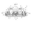
本実施の形態1の半導体装置は、図1に示すように、配線基板上にアナログ半導体素子であるアナログチップ101と、ディジタル半導体素子であるディジタルチップ102が実装された半導体パッケージである。本実施の形態1では前記半導体パッケージの一例として、配線基板であるパッケージ基板51上にアナログ系のアナログチップ101と、ディジタル系のディジタルチップ102が混載された樹脂封止型のSIP(System In Package)10を取り上げて説明する。 As shown in FIG. 1, the semiconductor device of the first embodiment is a semiconductor package in which an
パッケージ基板51の主面上に実装されたアナログチップ101は、例えば、RFタイプのものであり、図23に示すように、例えばアンテナ94が接続されて電波の送受信を行う。他方、同じくパッケージ基板51の主面上に実装されたディジタルチップ102は、例えば、マイクロプロセッサ等であり、種々の処理の制御を行う。 The
図1に示すように、アナログチップ101及びディジタルチップ102は、それぞれの主面をパッケージ基板51側に向けてバンプ(接続端子)20を介してパッケージ基板51にフリップチップ接続されている。さらに、パッケージ基板51上で、アナログチップ101及びディジタルチップ102は封止用樹脂によって形成された封止体30によって封止されている。 As shown in FIG. 1, the
また、SIP10のパッケージ基板51の裏面には、図7に示すように、複数の外部端子である半田ボール71が格子状に配置されて設けられており、SIP10はBGA(Ball Grid Array)タイプの半導体パッケージでもある。なお、複数の半田ボール71のそれぞれは、アナログチップ101及びディジタルチップ102それぞれの接続端子に対応してこれらとパッケージ基板51の内部配線を介して電気的に接続されている。したがって、アナログチップ101及びディジタルチップ102は、それぞれに対応して電気的に接続された半田ボール71を介して外部との信号のやり取りを行っている。 Further, as shown in FIG. 7,
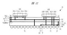
本実施の形態1のSIP10では、図3に示すように、そのパッケージ基板51の内部に、2つの異なったインピーダンスを有する配線パターンを図9に示すような単位セル(単位配線パターン)52cとしてこの単位セル52cが平面上に複数配置されてなるEBG配線部52が形成されている。さらに、EBG配線部52の一方の端に接続されたディジタル用電源配線部(ディジタル素子用電源配線部)54Dと、EBG配線部52の反対側の他方の端に接続されたアナログ用電源配線部(アナログ素子用電源配線部)54Aと、グランド配線部53とが形成されている。なお、ディジタル用電源配線部54Dとアナログ用電源配線部54Aは、同一配線層に配置されている。 In the
すなわち、ディジタル用電源配線部54Dとアナログ用電源配線部54AがEBG配線部52を介して電気的に接続されており、その際、ディジタル用電源配線部54Dは、EBG配線部52の一端でEBG接続用ビア(ビア配線)61を介してEBG配線部52と接続し、一方、アナログ用電源配線部54Aは、EBG配線部52の反対側の他端で同じくEBG接続用ビア61を介してEBG配線部52と接続している。つまり、ディジタル用電源配線部54Dとアナログ用電源配線部54Aは、EBG配線部52の両端に配置されたビア配線(EBG接続用ビア61)によってそれぞれ直流的に接続されているが、特定の高周波帯域で遮断される。 That is, the digital power
また、図3に示すように、グランド配線層(G)であるグランド配線部53は、アナログ用電源配線部54AとEBG配線部52の間に配置されており、さらにアナログ用電源配線部54Aは、EBG配線部52に対してアナログチップ101により近接して配置されている。すなわち、アナログ用電源配線部54AとEBG配線部52の間に両者をセパレートするグランド配線部53が配置され、さらにアナログチップ101は、アナログ用電源配線部54Aの近くに配置されている。アナログ用電源配線部54AとEBG配線部52の間にグランド配線部53が配置されていることにより、アナログ用電源配線部54AとEBG配線部52との間の電気結合を抑えてノイズ電力の漏れを防止することができる。 As shown in FIG. 3, the
次に、図4は電源層(V)を示すものである。図4に示すように、ディジタル用電源配線部54Dとアナログ用電源配線部54Aとは同一配線層に配置されており、その際、ディジタル用電源配線部54Dの方がアナログ用電源配線部54Aよりも面積が大きい。これは、ディジタルチップ102の方が高速処理でノイズの発生量も多いためであり、電源配線部の面積を大きくして電源の安定化を図ることができる。 Next, FIG. 4 shows a power supply layer (V). As shown in FIG. 4, the digital power
さらに、ディジタル用電源配線部54Dとアナログ用電源配線部54Aの間には、長さT以上の間隔が形成されており、これにより、電源ノイズの干渉を抑えることができる。Tは、例えば1mmであり、Tが1mmより小さいと両側の電気結合による電源ノイズの干渉を抑えることが困難になる。 Further, an interval of a length T or more is formed between the digital power
また、ディジタル用電源配線部54Dの外側の端部には複数のEBG接続用ビア61が接続されており、さらに、内側の端部及び中央付近には、複数のディジタル電源接続用ビア(ビア配線)64が接続されている。一方、アナログ用電源配線部54Aの外側の端部には複数のEBG接続用ビア61が接続されている。 A plurality of EBG connection vias 61 are connected to the outer end of the digital power
次に、図5はグランド層(G)を示すものである。図5に示すように、グランド配線部53は、パッケージ基板51とほぼ同じ面積(大きさ)で形成された大面積パターンであり、この大面積パターンには複数のアンチパッド(穴)62と、アンチパッド(穴)63が形成されている。EBG接続用ビア61はアンチパッド62の領域を通り、よってグランド配線部53とは接続せずにグランド配線部53の上下層を接続する。同様に、ディジタル電源接続用ビア64はアンチパッド63の領域を通りグランド配線部53とは接続せずにグランド配線部53の上下層を接続する。複数のEBG接続用ビアホールアンチパッド62は、グランド配線部53の両端に形成され、電源接続用ビアホールアンチパッド63は、EBG接続用ビアホールアンチパッド62より内側に形成されている。なお、図5
,図6ではアンチパッド62,63内のビア61,64は見やすさのため省略してある。Next, FIG. 5 shows a ground layer (G). As shown in FIG. 5, the
In FIG. 6, the
次に、図6はEBG層(V(EBG))を示すものである。図6に示すように、EBG配線部52には、その両端に複数のEBG接続用ビア61が形成され、さらに、EBG接続用ビア61の内側に複数の電源接続用ビアホールアンチパッド63が形成されている。すなわち、本実施の形態1のSIP10のパッケージ基板51では、EBG配線部52がパッケージ基板51の平面方向全体に亘ってパッケージ基板51とほぼ同面積で形成されており、さらに、EBG配線部52の両端にディジタル用電源配線部54Dまたはアナログ用電源配線部54Aに接続されるEBG接続用ビア61が接続されているため、EBGパターンを可能な限り長い距離で用いて電源ノイズのノイズ遮断効果を高めることができる。 Next, FIG. 6 shows an EBG layer (V (EBG)). As shown in FIG. 6, a plurality of EBG connection vias 61 are formed at both ends of the
以上により、ディジタル用電源配線部54DとEBG配線部52とがEBG配線部52の一端でEBG接続用ビア61を介して接続しており、他方、アナログ用電源配線部54AとEBG配線部52とがEBG配線部52の他端でEBG接続用ビア61を介して接続している。その際、EBG接続用ビア61は、グランド配線部53のアンチパッド62の領域を通ってグランド配線部53の上下の配線層を接続している。 As described above, the digital power
さらに、ディジタル用電源配線部54Dとこれに対応する図7に示す外部端子である半田ボール71は、グランド配線部53に形成された電源接続用ビアホールアンチパッド63及びEBG配線部52に形成されたアンチパッド63を通るディジタル電源接続用ビア64を介して直接接続されている。すなわち、ディジタル用電源配線部54Dは、EBG配線部52を介さず、ディジタル電源接続用ビア64を介して直接半田ボール71に接続されており、一方、アナログ用電源配線部54Aは、EBG配線部52を介して半田ボール71に接続されている。したがって、SIP10が図22に示すプリント基板80に実装された際には、SIP10のディジタル用電源配線部54Dは、ディジタル電源接続用ビア64と半田ボール71を介してプリント基板80の電源層である電源配線部82に接続される。 Furthermore, the digital power
なお、図3のP部に示すように、SIP10では、ディジタル用電源配線部54Dへの給電は、半田ボール71からディジタル電源接続用ビア64を通じて給電され、また、アナログ用電源配線部54Aへの給電は、ディジタル用電源配線部54Dを通った後、端部のEBG接続用ビア61を介してEBG配線部52に伝わり、EBG配線部52を端から端まで通った後、反対側の端部のEBG接続用ビア61を介してアナログ用電源配線部54Aに給電されることでなされる。 As shown in part P of FIG. 3, in the
また、ディジタルチップ102のグランド接続端子22Dと、アナログチップ101のグランド接続端子22Aは、それぞれ同一のグランド配線層(G)であるグランド配線部53に接続されている。 Further, the
すなわち、ディジタルチップ102のグランド接続端子とアナログチップ101のグランド接続端子は、共用のグランド配線部53に接続されている。 That is, the ground connection terminal of the
さらに、ディジタルチップ102の電源接続端子21Dは、ディジタル用電源配線部54Dに接続され、他方、アナログチップ101の電源接続端子21Aは、アナログ用電源配線部54Aに接続されている。 Furthermore, the power
次に、EBG配線部52の構造とその特性について説明する。 Next, the structure and characteristics of the
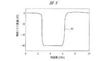
EBG配線部52は、図9に示すように、2つの異なったインピーダンスを有する配線パターンを単位セル(単位配線パターン)52cとして、この単位セル52cが平面上に周期的または規則的に複数配置されてなるものである。例えば、単位セル52cが、2つの異なった面積(大きさ)の第1配線パターン52aと第2配線パターン52bとから構成され、複数の単位セル52cが周期的または規則的に配置されることにより、電源の通過特性に図8に示すバンドギャップ(ある特定の周波数帯域で電源ノイズを遮断する特性)60を有するものである。図8に示すバンドギャップ60の例では、おおよそ周波数が3〜6GHzの範囲で電源が遮断され、電力すなわちエネルギはディジタル用電源配線部54Dからアナログ用電源配線部54Aに−60dBと減衰し伝わらない。 As shown in FIG. 9, the
次に遮断周波数(バンドギャップ)60が生じるメカニズムを説明する。EBG配線部52で電源の遮断が起こるのは、EBGパターンにおいて図9に示すように電源層に隙間(スリット)52dが形成されており、この隙間52dにより、EBG電源層を流れる電流の腹となる共振周波数では共振モードが立てない。逆に節となる共振はモードが立てる。この2つは周波数が異なるため、その結果として通過できる周波数と通過できない周波数が発生する。これら周波数の設定は、EBGパターンの物理的寸法、異なる比誘電率の材料または単位セル52cのインピーダンスと伝達時間の組み合わせで選択的に設定可能である。 Next, a mechanism for generating the cutoff frequency (band gap) 60 will be described. In the
例えば、図9に示すEBG配線部52のEBGパターンでは、大きな四角形の第1配線パターン52aと、小さな四角形の第2配線パターン52bを組み合わせた配線パターンを単位セル(単位配線パターン)52cとして、この単位セル52cを周期的または規則的に配置している。大きな四角形の第1配線パターン52aはグランド層に対して低いインピーダンスを持ち、一方、小さな四角形の第2配線パターン52bはグランド層に対して高いインピーダンスを持つため、インピーダンスの異なる2つの配線パターンを周期的に配置した構造である。 For example, in the EBG pattern of the
また、図10に示す変形例は、EBG配線部52における2つの異なった面積の配線パターンのうち、第2配線パターン52bをL字形に形成するものであり、これにより、L字形の第2配線パターン52bを隣接する単位セル52cに接続することが可能になる。その結果、第2配線パターン52bのインダクタンスを大きくすることができ、図9の単位セル52cと同じ面積でさらに大きなインピーダンスを持たすことが可能になる。したがって、図10に示すEBG配線部52の場合、図9に示すEBG配線部52と同じ面積であっても遮断する周波数を変えることができる。もしくは、図10に示すEBG配線部52では、図9に示すEBG配線部52と同じ周波数においても、より小さい面積で遮断特性を実現することができる。 Further, in the modification shown in FIG. 10, the
また、図11に示す変形例のEBG配線部52では、L字形の第2配線パターン52bをさらに長くすることで、図10のEBG配線部52で得られる効果をさらに増やすことが可能になる。 Further, in the
次に、SIP10では、図2及び図3に示すように、デカップリングキャパシタンス(コンデンサ素子)103が、アナログ用電源配線部54Aとグランド配線部53との間に接続されている。すなわち、パッケージ基板51上に、アナログ用電源配線部54Aとグランド配線部53とを電気的に接続するアナログ用デカップリングキャパシタンス103が搭載されている。これにより、アナログの電源の強化及び安定化を図ることができる。さらに、パッケージ基板51上には、ディジタル用電源配線部54Dとグランド配線部53とを電気的に接続するデカップリングキャパシタンス104が搭載されている。 Next, in the
本実施の形態1のSIP10によれば、パッケージ基板51上にアナログ系のアナログチップ101と、ディジタル系のディジタルチップ102が混載された半導体装置において、電源干渉を低減しつつ、高密度実装の実現を図ることができる。すなわち、SIP10においては、パッケージ基板51のEBG配線部52の一端にアナログ用電源配線部54Aが接続され、かつ他端にディジタル用電源配線部54Dが接続されているとともに、それぞれの素子用グランド接続端子が共通のグランド配線部53に接続されている。さらに、アナログ用電源配線部54AとEBG配線部52との間に両者をセパレートするグランド配線部53が設けられているとともに、アナログ用電源配線部54AがEBG配線部52から遠い位置に配置されている。 According to the
したがって、アナログ用電源配線部54AとEBG配線部52の間にグランド配線部53が設けられ、かつアナログ用電源配線部54AがEBG配線部52から遠い位置に配置されたことでEBGとアナログ用電源配線部54Aとの電気結合を抑えノイズの漏れを防ぐことができる。さらに、EBG配線部52をパッケージ基板51の大きさと同程度に最大限長く使用することが可能になるため、ノイズを遮断する特性をより向上させることができる。 Accordingly, the
その結果、SIP(半導体装置)10においてアナログチップ101への電源ノイズ干渉を低減しつつ高密度実装の実現を図ることができる。 As a result, in the SIP (semiconductor device) 10, it is possible to realize high-density mounting while reducing power supply noise interference to the
さらに、アナログチップ101への電源干渉を低減できるため、SIP10の信号の品質を確保できるとともに、電源の安定化を図ることができる。 Furthermore, since power supply interference to the
本実施の形態は、パッケージ基板51におけるEBG配線部52を含む配線パターンの変更のみで実現が可能なため、余分な部品を必要とせず低コストで電源干渉の低減化と高密度実装の実現化を図ることができる。 Since this embodiment can be realized only by changing the wiring pattern including the
なお、本実施の形態のSIP10では、上述のようにパッケージ基板の大きさに迫る長さのEBG配線部が介在することにより最大限の効果を得ている。一方、必要なノイズ遮断の効果を得るのに充分な長さのEBGパターンを介在されば良いので、パッケージ基板の部分的な領域のみをEBG配線部にする構造でも発明の効果を発揮できる。 In the
(実施の形態2)
図12は本発明の実施の形態2の半導体装置のパッケージ基板における内部配線の引き回しの一例を示す構造図である。(Embodiment 2)
FIG. 12 is a structural diagram showing an example of the routing of internal wiring in the package substrate of the semiconductor device according to the second embodiment of the present invention.
本実施の形態2のSIP(半導体装置)10は、ディジタル用電源配線部54Dをパッケージ基板51の裏面に近い側に配置したものである。すなわち、ディジタル用電源配線部54DをEBG配線部52と半田ボール71の間に配置したものである。これにより、ディジタル用電源配線部54Dの配線層を含む層において、アナログ用電源配線部54Aの直下に対応する領域にディジタル信号用の配線を形成することが可能になり、配線使用率を向上できる。 In the SIP (semiconductor device) 10 according to the second embodiment, the digital power
なお、ディジタル用電源配線部54Dをパッケージ基板51の裏面に近い側に配置したことで、ディジタル電源接続用ビア64を短くしてディジタル用電源配線部54Dを半田ボール71と最短で接続することができる。これにより、低インピーダンスでプリント基板80(図22参照)に接続することができ、ディジタルノイズを低減することができる。 Since the digital power
また、アナログ用電源配線部54Aの配線層を含む層において、ディジタル用電源配線部54Dの直上に対応する領域にアナログ信号用の配線を形成することが可能になり、前記同様、配線使用率を向上できる。 In addition, in the layer including the wiring layer of the analog power
なお、ディジタル用電源配線部54Dは、半田ボール71に低インピーダンスで接続されているため、EBGの遮断効果に影響を及ぼすことはない。したがって、本実施の形態2のSIP10も、実施の形態1のSIP10と同様の効果を得ることができる。 Since the digital power
(実施の形態3)
図13は本発明の実施の形態3の半導体装置のパッケージ基板における内部配線の引き回しの一例を示す構造図である。(Embodiment 3)
FIG. 13 is a structural diagram showing an example of the routing of internal wiring in the package substrate of the semiconductor device according to the third embodiment of the present invention.
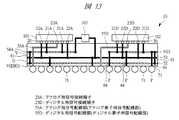
本実施の形態3のSIP(半導体装置)10は、アナログチップ101とディジタルチップ102それぞれの信号配線を示したものである。アナログ用信号配線部(アナログ素子用信号配線部)55Aは、アナログ用電源配線部54Aまたはグランド配線部53に隣接して引き回されてアナログチップ101と半田ボール71とを接続している。例えば、アナログ用信号配線部55Aは、アナログチップ101とアナログ用電源配線部54Aの間においてアナログ用電源配線部54Aに沿って配置され、さらにアナログチップ101用の信号接続端子であるアナログ用信号接続端子23Aとアナログ信号用の半田ボール71とを接続している。 The SIP (semiconductor device) 10 of the third embodiment shows signal wirings of the
このように、アナログ用信号配線部55Aをアナログ用電源配線部54Aまたはグランド配線部53に隣接して配置することにより、アナログ信号のリターン電流をアナログ用電源配線部54Aまたはグランド配線部53に流すことができる。すなわち、アナログ用信号配線部55AをEBG配線部52に隣接させると、アナログ信号のリターン電流がEBG層を流れることになり、特定の周波数で信号が伝搬できないことになる。このことを避けるためにアナログ用信号配線部55AをEBG配線部52に隣接させずにアナログ用電源配線部54Aまたはグランド配線部53に隣接させる。 As described above, by arranging the analog
同様に、ディジタル用信号配線部(ディジタル素子用信号配線部)55Dは、ディジタルチップ102とディジタル用電源配線部54Dの間においてディジタル用電源配線部54Dに沿って配置され、さらにディジタルチップ102用の信号接続端子であるディジタル用信号接続端子23Dとディジタル信号用の半田ボール71とを接続している。アナログ信号の場合と同様に、ディジタル信号のリターン電流をEBG層ではなくディジタル用電源配線部54Dまたはグランド配線部53に流すことができる。 Similarly, a digital signal wiring portion (digital element signal wiring portion) 55D is disposed along the digital power
なお、図13に図示したSIP10の、信号配線部55Aが接続された半田ボールの隣に位置する半田ボールを、EBG配線部52とビアで接続し、この半田ボールをアナログ信号用の接続端子と対を成す電源接続端子とする変形が可能である。この変形によれば、SIPの外部に接続する回路装置に至るまで、信号経路と近接したリターン経路を形成することが可能で、これによりノイズ混入を更に低下することができる。 Note that the solder ball located next to the solder ball to which the
(実施の形態4)
図14は本発明の実施の形態4の半導体装置のパッケージ基板に設けられたアナログ素子用電源配線部とディジタル素子用電源配線部の構造の一例を示す平面図、図15は本発明の実施の形態4の半導体装置のパッケージ基板に設けられたグランド配線部の構造の一例を示す平面図である。さらに、図16は本発明の実施の形態4の半導体装置のパッケージ基板に設けられたEBG配線部の構造の一例を示す平面図、図17は本発明の実施の形態4の半導体装置の外部端子の配置状態の一例を示す裏面図である。(Embodiment 4)
FIG. 14 is a plan view showing an example of the structure of the analog element power supply wiring portion and the digital element power supply wiring portion provided on the package substrate of the semiconductor device according to the fourth embodiment of the present invention, and FIG. 15 shows an embodiment of the present invention. FIG. 25 is a plan view showing an example of a structure of a ground wiring portion provided on a package substrate of a semiconductor device according to
本実施の形態4は、EBG配線部52の変形例の構造を示すものである。図14は電源層(V)を示しており、アナログ用電源配線部54Aの面積が実施の形態1に比べて小さくなり、一方、ディジタル用電源配線部54Dの面積が大きくなった場合の構造を示すものである。このようにアナログ用電源配線部54Aの面積が小さくなった場合でも、アナログ用電源配線部54Aにおいて引き出し配線56を介してEBG接続用ビア61と接続することで、アナログ用電源配線部54AとEBG接続用ビア61とを確実に接続することができる。 The fourth embodiment shows a structure of a modified example of the
すなわち、面積が小さくなったアナログ用電源配線部54Aにおいて、幅の狭い引き出し配線56を形成し、この引き出し配線56にEBG接続用ビア61を接続することで、アナログ用電源配線部54AとEBG配線部52とを引き出し配線56及びEBG接続用ビア61を介して確実に接続することができる。なお、引き出し配線56は、例えば、EBG配線部52の単位セル52cの小さい面積の第2配線パターン52bと同等の幅程度の引き出し用の配線である。 That is, in the analog power
一方、ディジタル用電源配線部54Dは実施の形態1より大きな面積となっているため、ディジタル用電源配線部54Dにより多くのディジタル電源接続用ビア64を接続し、これらディジタル電源接続用ビア64を、図15のグランド配線層(G)に示すグランド配線部53の電源接続用ビアホールアンチパッド63及び図16のEBG層(V(EBG))に示すEBG配線部52の電源接続用ビアホールアンチパッド63に通して、図17に示す外部端子である半田ボール71に直接接続している。 On the other hand, since the digital power
このようにディジタル側では、より多くのディジタル電源接続用ビア64を介してディジタル用電源配線部54Dと半田ボール71を接続しているため、ディジタルチップ102から発生するノイズを小さくすることができる。 In this way, on the digital side, the digital power
これにより、消費電力が大きく、かつ高いクロック周波数を有するディジタルチップ102であってもEBG配線部52により電源ノイズを遮断することができる。 As a result, even the
その結果、ディジタルチップ102のディジタル回路の給電インピーダンスを低下させて、SIP(半導体装置)10の信号の品質をさらに向上できる。 As a result, the power supply impedance of the digital circuit of the
なお、図14に示すようにディジタル用電源配線部54Dとアナログ用電源配線部54Aの間には、T以上の間隔が必要である。例えば、T=1mmである。これにより、ディジタル電源ノイズがディジタル用電源配線部54Dからアナログ用電源配線部54Aに直接干渉することを阻止できる。 As shown in FIG. 14, an interval of T or more is required between the digital power
(実施の形態5)
図18は本発明の実施の形態5の半導体装置のパッケージ基板に設けられたアナログ素子用電源配線部とディジタル素子用電源配線部の構造の一例を示す平面図、図19は本発明の実施の形態5の半導体装置のパッケージ基板のグランド配線部に設けられた第1のEBG配線部の構造の一例を示す平面図である。さらに、図20は本発明の実施の形態5の半導体装置のパッケージ基板に設けられた第2のEBG配線部の構造の一例を示す平面図、図21は本発明の実施の形態5の半導体装置の外部端子の配置状態の一例を示す裏面図である。(Embodiment 5)
FIG. 18 is a plan view showing an example of the structure of the analog element power supply wiring portion and the digital element power supply wiring portion provided on the package substrate of the semiconductor device according to the fifth embodiment of the present invention, and FIG. FIG. 38 is a plan view showing an example of a structure of a first EBG wiring portion provided in a ground wiring portion of a package substrate of a semiconductor device according to mode 5. 20 is a plan view showing an example of the structure of the second EBG wiring portion provided on the package substrate of the semiconductor device according to the fifth embodiment of the present invention. FIG. 21 is a semiconductor device according to the fifth embodiment of the present invention. It is a reverse view which shows an example of the arrangement | positioning state of this external terminal.
図18〜図21に示す本実施の形態5は、EBG配線部52の他の変形例の構造を示すものであり、図18に示す電源層(V)に対してEBGパターンをグランド用とディジタル用で2つ有するものである。すなわち、図20に示すEBG層(V(EBG))の電源用EBG配線部(第2のEBG配線部)58に加えて、図19に示すグランド層(G)であるグランド配線部53にもグランド用EBG配線部(第1のEBG配線部)57を形成したものである。 The fifth embodiment shown in FIGS. 18 to 21 shows the structure of another modified example of the
このようにグランド配線部53にもグランド用EBG配線部57を形成したことにより、EBG層の電源用EBG配線部58と対になるため、ノイズ遮断の効果をより大きくすることができる。 Since the ground
(実施の形態6)
図22は本発明の実施の形態6の半導体装置の実装状態における内部配線の引き回しの一例を示す構造図である。(Embodiment 6)
FIG. 22 is a structural diagram showing an example of internal wiring routing in the mounted state of the semiconductor device according to the sixth embodiment of the present invention.
本実施の形態6は、SIP10のプリント基板80への実装時の配線の接続について説明するものである。SIP10のグランド配線部53はプリント基板80のグランド配線部81に接続され、かつディジタル用電源配線部54Dはプリント基板80の電源配線部82に接続される。ただし、アナログ用電源配線部54Aは直接半田ボール71に接続されておらず、必ずEBG配線部52を介して接続されている。 In the sixth embodiment, connection of wiring when mounting the
アナログ用電源配線部54Aが、EBG配線部52を介することなく、半田ボール71に接続された構造では、ディジタル用電源配線部54Dとグランド配線部53の間に誘起された電源ノイズが、プリント基板80の電源配線部82とグランド配線部81の間に伝搬され、電源配線部82からアナログ用電源配線部54Aに伝搬してしまう。すなわちSIP10内のEBG配線部52によるノイズの低減の効果を損ねてしまう。これを避けるため、アナログ用電源配線部54Aは、必ずEBG配線部52を介して半田ボール71に接続されている。 In the structure in which the analog power
なお、プリント基板80上にはオンボードデカップリングキャパシタンス105が搭載されているため、このオンボードデカップリングキャパシタンス105によりプリント基板80でのノイズ低減が図られている。 Since the on-
(実施の形態7)
図23は本発明の実施の形態7の半導体装置の使用例の一例を示すブロック図であり、SIP10をディジタルカメラ90に組み込んだ例の構成を示すものである。(Embodiment 7)
FIG. 23 is a block diagram showing an example of a usage example of the semiconductor device according to the seventh embodiment of the present invention, and shows a configuration of an example in which the
ディジタルカメラ90に組み込まれたEBGパターン内蔵のSIP10において、レンズ92を通って撮像素子91で撮影されたイメージ情報をSIP10内のディジタル処理部であるディジタルチップ102で処理し、さらに表示部93で表示する。一方、プリンタやパーソナルコンピュータ、インターネットのwebサーバにアンテナ94を介して通信するためのアナログ処理をRF部であるアナログチップ101で処理する。双方の処理が行われる際に、主にディジタルチップ102から発生される電源ノイズをノイズ遮断手段95によって遮断する。実施の形態1〜7においてこのノイズ遮断手段95がパッケージ基板51に形成されたEBG配線部52(グランド用EBG配線部57及び電源用EBG配線部58も含む)である。 In the
(実施の形態8)
図24は本発明の実施の形態8の半導体装置の断面図を示す。本実施の形態8の半導体装置は、アナログチップ101とディジタルチップ102とが積層された構造を有する。アナログチップ101は、その主面がパッケージ基板51の側に向けられ、パッケージ基板51にフリップチップ接続される。ディジタルチップ102はアナログチップ101の上に、主面を外側にして積層される。(Embodiment 8)
FIG. 24 is a sectional view of the semiconductor device according to the eighth embodiment of the present invention. The semiconductor device according to the eighth embodiment has a structure in which an
パッケージ基板51の内部には、半田ボール71が2次元アレイ状に配置された面に近い層から順に、電源配線部54、EBG配線部52、グランド配線部53がある。更にその上の層の中心領域には、アナログチップ用電源配線部54Aが設けられる。アナログチップ101のグランド接続端子はグランド配線部53にビアホール65を介して接続される。またアナログチップ101の電源接続端子はアナログ用電源配線部54Aにビアホール66を介して接続される。電源配線部54と外部接続用の半田ボール71とはビアホール接続される。その電源配線部54とEBG配線部52とはビアホール61Dで接続される。EBG配線部52とアナログチップ用電源配線部54Aとは、EBG配線部52のビアホール61Dの位置とは反対の端部に位置するビアホール61Aで接続される。 Inside the
一方、パッケージ基板51のEBG配線部52と同じ深さの層の端の領域には、ディジタルチップ用電源配線部54Dが設けられる。ディジタルチップ用電源配線部54Dは電願配線部54とビアホール64で接続され、さらにディジタルチップ用電源配線部54Dは電源接続用パッド72Pとビアホール67で接続される。またグランド層53はグランド接続用パッド73Pとビアホール69により接続される。電源配線部54に直接繋がるビアホール61Dにも別の電源接続用パッド72P′が接続されている。これら電源接続用パッド72P、72P′及びグランド接続用パッド73Pとディジタルチップ102とが、それぞれボンンディングワイヤ72、73で接続される。なお図では省略したが、上記の電源配線及びグランドの配線の他に信号の配線等が存在する。さらに、これらアナログチップ及びディジタルチップは封止用樹脂(図では省略)で封止されてパッケージ基板51と一体化されている。 On the other hand, in the region of the end of the layer having the same depth as the
本実施の形態8の半導体装置では、アナログ用電源配線部54Aには、EBG配線部52を介して給電がなされる。また、アナログ用電源配線部54AとEBG配線部52の間にグランド配線部53の層が存在する。これら2点は、図3などを参照して説明した実施の形態1と類似であり、ディジタルチップとアナログチップとの間のノイズ遮断の上で実施の形態1の半導体装置と同様な効果が得られる。 In the semiconductor device of the eighth embodiment, power is supplied to the analog power
(実施の形態9)
図25は本発明の実施の形態9の半導体装置の断面を示す。この半導体装置では、パッケージ基板51のグランド配線部53の層から上の、ディジタルチップ102に至る部分の構造は、実施の形態8の半導体装置と全く変わりがない。(Embodiment 9)
FIG. 25 shows a cross section of the semiconductor device according to the ninth embodiment of the present invention. In this semiconductor device, the structure from the layer of the
図26(a) は実施の形態9の半導体装置のパッケージ基板51のアナログ用電源配線部54Aが存在する層の平面図である。図26(b) はグランド配線部53が存在する層の平面図である。図26(d) はパッケージ基板裏面の平面図である。これらの平面図は、実施の形態8の半導体装置でも共通となる。 FIG. 26A is a plan view of a layer in which the analog power
図26(c) は、実施の形態9の半導体装置のパッケージ基板51のEBG配線部52が存在する面の平面図である。図26(a) 〜図26(d) 、及び図25で示されるとおり、EBG配線部52はパッケージ基板51の中程の領域にのみ形成され、右左の両端近くの領域には、それぞれ一様な金属層でなるディジタルチップ用電源配線部54D1、及び54D2が形成される。ディジタルチップ用電源配線部54D1はEBG配線部52に接している。別の言葉で述べると、両者の境界位置54Tでは、一様な金属膜からEBGパターンの金属膜へとパターンが変化する。EBG配線部52から分離されたディジタルチップ用電源配線部54D2は、ビアホール64により外部からの電源供給のための半田ボール712に接続され、またビアホール67によりディジタルチップ102に電源を繋ぐためのパッド72Pにも接続されている。ディジタルチップ用電源配線部54D1は、ディジタルチップ102に電源を繋ぐための別のパッド72P′、及び外部からの電源供給のための別の半田ボール711にビアホール61Dにより接続されている。更に、EBG配線部52は、ディジタルチップ用電源配線部54D1に接している側と逆の端部近くにあるビアホール61Aによりアナログチップ用電源配線部54Aに接続されている。図26(b) にはビアホール67,61A,61Dがそれぞれグランド配線部53と非接触に通過するようにグランド配線部53に設けられたアンチパッド68,62A,62Dが示される。これにより、アナログチップ101への電源の供給経路が形成される。 FIG. 26C is a plan view of the surface on which the
本実施の形態9においても、アナログチップ用電源配線部はグランド層により隔離されて配置されるとともに、ディジタルチップへの電源供給経路との間にEBG配線部が介在する構成となっている。よって、電源供給経路を介したディジタルチップとアナログチップ間のノイズ漏洩の防止の点で実施の形態8の半導体装置と同等な効果を得ることができる。 Also in the ninth embodiment, the analog chip power supply wiring portion is arranged isolated by the ground layer, and the EBG wiring portion is interposed between the power supply path to the digital chip. Therefore, an effect equivalent to that of the semiconductor device of the eighth embodiment can be obtained in terms of preventing noise leakage between the digital chip and the analog chip via the power supply path.
(実施の形態10)
図27は実施の形態10の半導体装置の断面を示す。本実施の形態10の半導体装置はアナログチップ101、ディジタルチップ102の積層順が実施の形態8もしくは実施の形態9の半導体装置と逆になっている。ディジタルチップ102は、その主面がパッケージ基板51の側に向けられ、パッケージ基板51にフリップチップ接続される。アナログチップ101はそのディジタルチップ102の上に、主面を外側にして積層される。(Embodiment 10)
FIG. 27 shows a cross section of the semiconductor device of the tenth embodiment. In the semiconductor device of the tenth embodiment, the stacking order of the
図28(a) は実施の形態10のパッケージ基板51の個別電源層の平面図、図28(b) はグランド層の平面図、図28(c) はEBG層の平面図、図28(d) はパッケージ基板裏面の平面図である。 28A is a plan view of the individual power supply layer of the
これらの図面が示すように、パッケージ基板51の個別電源層にはアナログチップ用電源配線部54A1、ディジタル用電源配線部54D、もう一つのアナログチップ用電源配線部54A2が互いに分離して並ぶ。中央のディジタル用電源配線部54Dは基板裏面の半田ボール713とビアホール64により接続されており、これにより外部から電源が供給される。ディジタルチップ102の電源用バンプはディジタル用電源配線部54Dに繋がるビアホール67に接続される。またディジタルチップ102のグランド用バンプはグランド層のグランド配線部53に繋がるビアホール69に接続される。アナログチップ用電源配線部54A1と54A2には外部から直接ではなく、ディジタル用電源配線部54Dを介して電源が供給される。すなわち、EBG配線部52の中央部分がビアホール61によりディジタル用電源配線部54Dに接続され、EBG配線部52の両端部はビアホール611と612によりアナログチップ用電源配線部54A1,54A2にそれぞれ接続される。図28(b) に示すとおり、基板のほぼ全面を占めるグランド配線部53にはこれらのビアホール61,611,612が通過するアンチパッド62が設けられる。アナログチップ用電源配線部54A1,54A2には電源用パッド72Pがそれぞれ接続され、また、グランド層とグランド用パッド73Pとはビアホール66により接続される。電源用パッド72Pとアナログチップ101の間をボンディングワイヤ72で接続し、グランド用パッド73Pとアナログチップ101の間をボンディングワイヤ73で接続することでアナログチップ101への給電経路が完成する。 As shown in these drawings, an analog chip power supply wiring portion 54A1, a digital power
本実施の形態10では、アナログチップにいたる電源供給経路に、パッケージ基板の長さの概ね半分の有効長をもつEBGパターンが介在し、またEBG配線部はグランド配線部により隔離された位置に配置される。この構造により、ディジタルチップとアナログチップの間のノイズ漏洩が有効に防止される。 In the tenth embodiment, an EBG pattern having an effective length approximately half the length of the package substrate is interposed in the power supply path leading to the analog chip, and the EBG wiring portion is arranged at a position isolated by the ground wiring portion. Is done. With this structure, noise leakage between the digital chip and the analog chip is effectively prevented.
(実施の形態11)
図29は実施の形態11の半導体装置の断面を示す。本実施の形態11の半導体装置はフリップチップ接続により基板に積層されたディジタルチップの上に、さらにアナログチップをフリップチップ接続により積層したものである。パッケージ基板51の内部の各層の構造は実施の形態10のパッケージ基板51と変わりがない。同一部分には同一符号を付しているので図27、図28(a) 〜図28(d) の説明をも参照されたい。(Embodiment 11)
FIG. 29 shows a cross section of the semiconductor device of the eleventh embodiment. In the semiconductor device according to the eleventh embodiment, an analog chip is further laminated by flip-chip connection on a digital chip laminated on a substrate by flip-chip connection. The structure of each layer inside the
ディジタルチップ102の下面には半田ボールが配列しており、パッケージ基板51の上面に配列するパッドに圧着接続される。そのうち中程に位置する半田ボールのいくつかはディジタルチップ102の内部の回路に給電するための接続バンプであり、パッケージ基板51のディジタル配線部54Dにつながるビアホール67の先端のパッド、あるいはグランド配線部53につながるビアホール69の先端のパッドにそれぞれ接続される。 Solder balls are arranged on the lower surface of the
一方、ディジタルチップ102の周辺部には複数の貫通ビアホールが形成され、アナログチップ101とパッケージ基板51との間の電気接続がこれらの貫通ビアホールを介して行われる。半田ボール311がアナログチップ用電源配線部54A1から伸びたビアホール66の先端に接続されるので、貫通ビアホール301は電源VCCにつながる。同様に半田ボール313がアナログチップ用電源配線部54A2から伸びたビアホールの先端に接続されるので、貫通ビアホール303も電源VCCにつながる。一方、半田ボール312はグランド配線部53から伸びたビアホール65の先端に接続されるので、貫通ビアホール302はグランドVSSにつながる。半田ボール314はグランド配線部53から伸びた別のビアホールに接続されるので、貫通ビアホール304もグランドVSSにつながる。これらの貫通ビアホール301〜304のそれぞれの他端のパッドとアナログチップ101のパッドとは半田ボール351〜354によりそれぞれ接続され、これによりアナログチップ101への給電経路が形成される。なお、図29でも電源供給のための配線以外の配線は省略している。実際の半導体装置には、信号伝達の配線が存在する。好ましい例では、ディジタルチップとパッケージ基板との間の信号の伝達も、アナログチップに形成された貫通ビアホールを利用した信号経路を用いる。 On the other hand, a plurality of through via holes are formed in the peripheral portion of the
本実施の形態11でも、実施の形態10と同様にディジタルチップとアナログチップの間のノイズ漏洩が有効に防止される。 In the eleventh embodiment, as in the tenth embodiment, noise leakage between the digital chip and the analog chip is effectively prevented.
(実施の形態12)
図30は実施の形態12の半導体装置の断面を示す。本実施の形態12の半導体装置はアナログチップを搭載する基板とディジタルチップを搭載する基板とを有し、全体で複合パッケージ構造となっている。(Embodiment 12)
FIG. 30 shows a cross section of the semiconductor device of the twelfth embodiment. The semiconductor device of the twelfth embodiment has a substrate on which an analog chip is mounted and a substrate on which a digital chip is mounted, and has a composite package structure as a whole.
外部への接続用の半田ボールアレイを備えた基板51Dはグランド層53Dと電源層54Dを備える。電源層54Dは半田ボール713にビアホール64Dで接続されており、これにより、外部からディジタルチップ用の電源電圧VCCDが印加される。グランド層53Dは半田ボール714と接続され、これにより、グランド電圧VSSDが与えられる。ディジタルチップ102は基板51Dにフリップチップ接続されて電源層54Dとグランド層53Dに繋がり、これにより、電源の供給を受ける。また供給される電源の安定化のためのデカップリングキャパシタンス104が電源層54Dとグランド層53Dの間に接続される。 A
基板51Aは、その下側から順にEBG層52と、グランド層53Aと、電源層54Aとを備える。いずれの層も基板51Aのほぼ端から端に渡って形成されている。基板51Aは金属ピン321及び322により基板51Dに固定されている。これら金属ピンはアナログチップ101へ電源を供給する経路の一部になっている。すなわち基板51AのEBG層52の一方の端部は基板51Dの電源層54Dと、ビアホール64A、金属ピン321及びビアホール64Dを介して接続される。さらにEBG層52の他方の端部と電源層54Aはビアホール61を介して接続される。また、基板51Aのグランド層53Aはビアホール65A、金属ピン322及びビアホール65Dを介して基板51Dのクランド層53Dと接続される。アナログチップ101は基板51Dにフリップチップ接続されて電源層54Dとグランド層53Dに繋がり、これにより、電源の供給を受ける。電源層54Dとグランド層53Dの間に、電源安定化のためのデカップリングキャパシタンス103が接続される。 The
以上によるアナログチップ101への電源供給経路には、EBG層52が介在するので、他の実施の形態と同様にアナログチップとディジタルチップ間のノイズ遮断がなされる。 Since the
(実施の形態13)
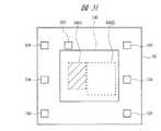
図31は実施の形態13の半導体装置の平面図、図32は同半導体装置の断面図である。本実施の形態13の半導体装置では、アナログ集積回路とディジタル集積化路の両方を形成した半導体チップを用いる。(Embodiment 13)
FIG. 31 is a plan view of the semiconductor device according to the thirteenth embodiment, and FIG. 32 is a cross-sectional view of the semiconductor device. In the semiconductor device of the thirteenth embodiment, a semiconductor chip in which both an analog integrated circuit and a digital integrated path are formed is used.
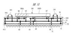
半導体チップ100の一部領域100Aにはアナログ集積回路が形成される。以下では、これをアナログ部100Aと呼ぶ。また、これと隣接する別の領域100Dにはディジタル集積回路が形成される。以下ではこれをディジタル部100Dと呼ぶ。アナログ部100Aとディジタル部100Dは、それぞれ別の電源用バンプおよびグランド用バンプを備え、これらにより個別に給電可能な構造となっている。 An analog integrated circuit is formed in a
パッケージ基板51の構造は先に図3を用いて説明した実施の形態1のパッケージ基板と基本的に変わりがない。すなわちパッケージ基板51の下から順にEBG配線部52、グランド配線部53を備える。さらにその上の層の一部領域がアナログ用電源配線部54Aであり、別の領域がディジタル用電源配線部54Dである。EBG配線部52の一方の端とアナログ用電源配線部54Aがビアホール612を介して接続される。EBG配線部52の他方の端とディジタル用配線部54Dがビアホール61を介して接続される。半導体チップ100のディジタル部100Dの電源用バンプはディジタル用電源配線部54Dとビア67を介して接続され、グランド用バンプはグランド配線部53とビアホール65を介して接続される。半導体チップ100のアナログ部100Aの電源用バンプはアナログ用電源配線部54Aとビア66を介して接続される。電源供給用の半田ボール71とデジタル用電源配線部54Dがビア64を介して接続されており、グランド用の半田ボールとグランド配線部52が接続されている。 The structure of the
以上により、アナログ部100Aに至る電源供給経路の途中にはEBG配線部が介在し、これにより、ディジタル部100Dとアナログ部100Aとは直流的に接続されても特定高周波領域で遮断される。よってアナログ部とディジタル部の間のノイズ遮断の効果が得られる。 As described above, the EBG wiring portion is interposed in the middle of the power supply path leading to the
以上、本発明者によってなされた発明を発明の実施の形態に基づき具体的に説明したが、本発明は前記発明の実施の形態に限定されるものではなく、その要旨を逸脱しない範囲で種々変更可能であることは言うまでもない。 As mentioned above, the invention made by the present inventor has been specifically described based on the embodiments of the invention. However, the present invention is not limited to the embodiments of the invention, and various modifications can be made without departing from the scope of the invention. It goes without saying that it is possible.
例えば、前記実施の形態1〜7においては、半導体装置がBGAタイプの場合について説明したが、前記半導体装置の外部端子は半田ボール71に限らず、ランド等であってもよい。したがって、前記半導体装置は、LGA(Land Grid Array)等であってもよい。 For example, in the first to seventh embodiments, the case where the semiconductor device is the BGA type has been described. However, the external terminal of the semiconductor device is not limited to the
本発明は、アナログ半導体素子とディジタル半導体素子を有する電子装置に好適である。 The present invention is suitable for an electronic device having an analog semiconductor element and a digital semiconductor element.
10 SIP(半導体装置)
20 バンプ(接続端子)
21A アナログ用電源接続端子
21D ディジタル用電源接続端子
22A アナログ用グランド接続端子
22D ディジタル用グランド接続端子
23A アナログ用信号接続端子
23D ディジタル用信号接続端子
30 封止体
51 パッケージ基板(配線基板)
52 EBG配線部
52a 第1配線パターン
52b 第2配線パターン
52c 単位セル(単位配線パターン)
52d 隙間
53 グランド配線部
54A アナログ用電源配線部(アナログ素子用電源配線部)
54D ディジタル用電源配線部(ディジタル素子用電源配線部)
55A アナログ用信号配線部(アナログ素子用信号配線部)
55D ディジタル用信号配線部(ディジタル素子用信号配線部)
56 引き出し配線
57 グランド用EBG配線部(第1のEBG配線部)
58 電源用EBG配線部(第2のEBG配線部)
60 バンドギャップ
61 EBG接続用ビア(ビア配線)
62 EBG接続用ビアホールアンチパッド
63 電源接続用ビアホールアンチパッド
64 ディジタル電源接続用ビア(ビア配線)
71 半田ボール(外部端子)
80 プリント基板
81 グランド配線部
82 電源配線部
90 ディジタルカメラ
91 撮像素子
92 レンズ
93 表示部
94 アンテナ
95 ノイズ遮断手段
100 半導体チップ
101 アナログチップ(アナログ半導体素子)
102 ディジタルチップ(ディジタル半導体素子)
103 アナログ用デカップリングキャパシタンス(コンデンサ素子)
104 ディジタル用デカップリングキャパシタンス
105 オンボードデカップリングキャパシタンス10 SIP (semiconductor device)
20 Bump (connection terminal)
21A Analog
52
54D Digital power supply wiring section (digital element power supply wiring section)
55A Analog signal wiring section (analog element signal wiring section)
55D Digital signal wiring section (digital element signal wiring section)
56
58 EBG wiring section for power supply (second EBG wiring section)
60
62 Via hole antipad for
71 Solder balls (external terminals)
DESCRIPTION OF
102 Digital chip (digital semiconductor device)
103 Decoupling capacitance for analog (capacitor element)
104
Claims (23)
Translated fromJapanese電源接続端子及びグランド接続端子が接続されたアナログ半導体素子と、
前記ディジタル半導体素子と前記アナログ半導体素子が搭載された配線基板と、
前記配線基板に接続された複数の外部端子とを有し、
前記配線基板は、2つの異なったインピーダンスを有する配線パターンを単位配線パターンとして前記単位配線パターンが平面上に複数配置されてなるEBG配線部と、グランド配線部と、前記EBG配線部の一方の端に接続されたディジタル素子用電源配線部と、前記EBG配線部の他方の端に接続されたアナログ素子用電源配線部とを有し、
前記ディジタル半導体素子用の前記グランド接続端子と前記アナログ半導体素子用の前記グランド接続端子は、前記配線基板の前記グランド配線部に接続され、
前記ディジタル半導体素子用の前記電源接続端子は、前記配線基板の前記ディジタル素子用電源配線部に接続され、
前記アナログ半導体素子用の前記電源接続端子は、前記配線基板の前記アナログ素子用電源配線部に接続されていることを特徴とする半導体装置。A digital semiconductor element to which a power connection terminal and a ground connection terminal are connected;
An analog semiconductor element to which a power connection terminal and a ground connection terminal are connected;
A wiring board on which the digital semiconductor element and the analog semiconductor element are mounted;
A plurality of external terminals connected to the wiring board;
The wiring board includes an EBG wiring portion in which a plurality of unit wiring patterns are arranged on a plane using wiring patterns having two different impedances as a unit wiring pattern, a ground wiring portion, and one end of the EBG wiring portion. A power wiring portion for a digital element connected to a power wiring portion for an analog element connected to the other end of the EBG wiring portion,
The ground connection terminal for the digital semiconductor element and the ground connection terminal for the analog semiconductor element are connected to the ground wiring portion of the wiring board,
The power supply connection terminal for the digital semiconductor element is connected to the power supply wiring portion for the digital element of the wiring board,
The power supply connection terminal for the analog semiconductor element is connected to the analog element power supply wiring portion of the wiring board.
電源接続端子及びグランド接続端子が接続されたアナログ半導体素子と、
前記ディジタル半導体素子と前記アナログ半導体素子が搭載された配線基板と、
前記配線基板に接続された複数の外部端子とを有し、
前記配線基板は、2つの異なった面積の配線パターンの組み合わせからなる単位配線パターンが平面上に規則的に複数配置されてなるEBG配線部と、グランド配線部と、前記EBG配線部の一方の端に接続されたディジタル素子用電源配線部と、前記EBG配線部の他方の端に接続されたアナログ素子用電源配線部とを有し、
前記ディジタル半導体素子用の前記グランド接続端子と前記アナログ半導体素子用の前記グランド接続端子は、前記配線基板の前記グランド配線部に接続され、
前記ディジタル半導体素子用の前記電源接続端子は、前記配線基板の前記ディジタル素子用電源配線部に接続され、
前記アナログ半導体素子用の前記電源接続端子は、前記配線基板の前記アナログ素子用電源配線部に接続されていることを特徴とする半導体装置。A digital semiconductor element to which a power connection terminal and a ground connection terminal are connected;
An analog semiconductor element to which a power connection terminal and a ground connection terminal are connected;
A wiring board on which the digital semiconductor element and the analog semiconductor element are mounted;
A plurality of external terminals connected to the wiring board;
The wiring board includes an EBG wiring portion in which a plurality of unit wiring patterns each including a combination of wiring patterns having different areas are regularly arranged on a plane, a ground wiring portion, and one end of the EBG wiring portion. A power wiring portion for a digital element connected to a power wiring portion for an analog element connected to the other end of the EBG wiring portion,
The ground connection terminal for the digital semiconductor element and the ground connection terminal for the analog semiconductor element are connected to the ground wiring portion of the wiring board,
The power supply connection terminal for the digital semiconductor element is connected to the power supply wiring portion for the digital element of the wiring board,
The power supply connection terminal for the analog semiconductor element is connected to the analog element power supply wiring portion of the wiring board.
電源接続端子及びグランド接続端子が接続されたアナログ半導体素子と、
前記ディジタル半導体素子と前記アナログ半導体素子が搭載された配線基板と、
前記配線基板に接続された複数の外部端子とを有し、
前記配線基板は、2つの異なったインピーダンスを有する配線パターンを単位配線パターンとして前記単位配線パターンが平面上に複数配置されてなるEBG配線部をグランド用と電源用で2つ有し、
前記グランド用の第1のEBG配線部は、一方の端がディジタル素子用グランド配線部に接続され、他方の端がアナログ素子用グランド配線部に接続され、
前記電源用の第2のEBG配線部は、一方の端がディジタル素子用電源配線部に接続され、他方の端がアナログ素子用電源配線部に接続され、
前記ディジタル半導体素子用の前記グランド接続端子は、前記配線基板のディジタル素子用グランド配線部に接続され、
前記アナログ半導体素子用の前記グランド接続端子は、前記配線基板のアナログ素子用グランド配線部に接続され、
前記ディジタル半導体素子用の前記電源接続端子は、前記配線基板のディジタル素子用電源配線部に接続され、
前記アナログ半導体素子用の前記電源接続端子は、前記配線基板のアナログ素子用電源配線部に接続されていることを特徴とする半導体装置。A digital semiconductor element to which a power connection terminal and a ground connection terminal are connected;
An analog semiconductor element to which a power connection terminal and a ground connection terminal are connected;
A wiring board on which the digital semiconductor element and the analog semiconductor element are mounted;
A plurality of external terminals connected to the wiring board;
The wiring board has two EBG wiring portions for a ground and a power source in which a plurality of unit wiring patterns are arranged on a plane using a wiring pattern having two different impedances as a unit wiring pattern,
The first EBG wiring portion for the ground has one end connected to the digital element ground wiring portion, and the other end connected to the analog element ground wiring portion,
The second EBG wiring portion for power supply has one end connected to the power wiring portion for digital element and the other end connected to the power wiring portion for analog element.
The ground connection terminal for the digital semiconductor element is connected to a digital element ground wiring portion of the wiring board,
The ground connection terminal for the analog semiconductor element is connected to the analog element ground wiring portion of the wiring board,
The power supply connection terminal for the digital semiconductor element is connected to a power supply wiring portion for the digital element of the wiring board,
The power supply connection terminal for the analog semiconductor element is connected to an analog element power supply wiring portion of the wiring board.
前記配線基板にフリップチップ接続により搭載されるディジタル半導体素子と、
前記ディジタル半導体素子にさらに積層されるアナログ半導体素子とを有し、
前記配線基板には、2つの異なったインピーダンスを有する配線パターンを単位配線パターンとして前記単位配線パターンが平面上に複数配置されてなるEBG配線部と、グランド配線部と、前記EBG配線部の中央にビア配線により接続されたディジタル素子用電源配線部と、前記EBG配線部の両端にそれぞれビア配線により接続された複数のアナログ素子用電源配線部を有し、
前記ディジタル半導体素子の電源接続端子が前記ディジタル素子用電源配線部に、また前記ディジタル半導体素子のグランド接続端子が前記グランド配線部に、それぞれフリップチップ接続により電気接続され、
前記アナログ半導体素子の複数の電源接続端子と前記複数のアナログ素子用電源配線部とが、及び前記アナログ半導体素子のグランド接続端子と前記グランド配線部とがそれぞれ接続されていることを特徴とする半導体装置。A wiring board having a plurality of external terminals;
A digital semiconductor element mounted on the wiring board by flip chip connection;
An analog semiconductor element further stacked on the digital semiconductor element,
In the wiring board, two wiring patterns having different impedances are used as unit wiring patterns, and a plurality of the unit wiring patterns are arranged on a plane, an EBG wiring section, a ground wiring section, and a center of the EBG wiring section. A power wiring portion for digital elements connected by via wiring, and a plurality of power wiring portions for analog elements respectively connected by via wiring at both ends of the EBG wiring portion;
The power connection terminal of the digital semiconductor element is electrically connected to the power supply wiring part for the digital element, and the ground connection terminal of the digital semiconductor element is electrically connected to the ground wiring part by flip chip connection, respectively.
A plurality of power supply connection terminals of the analog semiconductor element and the plurality of power supply wiring portions for analog elements, and a ground connection terminal of the analog semiconductor element and the ground wiring portion are connected to each other. apparatus.
前記第1の配線基板に搭載されたディジタル半導体素子と
前記第1の配線基板に積層された第2の配線基板と、
前記第2の配線基板に搭載されたアナログ半導体素子とを有し、
前記第1の配線基板には、前記外部端子の一つと前記ディジタル半導体素子の電源端子との電気接続を行う第1の電源配線部と、前記外部端子の他の一つと前記ディジタル半導体素子のグランド端子との電気接続を行う第1のグランド配線部を有し、
前記第2の配線基板には、一端が前記第1の配線基板の第1の電源端子に接続され、2つの異なったインピーダンスを有する配線パターンを単位配線パターンとして前記単位配線パターンが平面上に複数配置されてなるEBG配線部と、前記第1の配線基板の第1のグランド端子に接続された第2のグランド配線部と、前記EGB配線部の他端と接続された第2の電源配線部を有し、
前記第2の電源配線部と前記アナログ半導体素子の電源接続端子とが電気接続され、前記第2のグランド配線部と前記アナログ半導体素子のグランド接続端子とが電気接続されることを特徴とする半導体装置A first wiring board having a plurality of external terminals;
A digital semiconductor element mounted on the first wiring board; a second wiring board stacked on the first wiring board;
An analog semiconductor element mounted on the second wiring board;
The first wiring board includes a first power supply wiring portion that electrically connects one of the external terminals and the power supply terminal of the digital semiconductor element, and the other one of the external terminals and the ground of the digital semiconductor element. A first ground wiring portion for electrical connection with the terminal;
One end of the second wiring board is connected to the first power supply terminal of the first wiring board, and a plurality of unit wiring patterns are formed on a plane using two wiring patterns having different impedances as unit wiring patterns. An EBG wiring portion arranged, a second ground wiring portion connected to the first ground terminal of the first wiring board, and a second power wiring portion connected to the other end of the EGB wiring portion Have
The second power supply wiring portion and a power connection terminal of the analog semiconductor element are electrically connected, and the second ground wiring portion and a ground connection terminal of the analog semiconductor element are electrically connected. apparatus
前記半導体チップを搭載し、かつ外部接続端子を備える配線基板とを有し、
前記配線基板には、
2つの異なったインピーダンスを有する配線パターンを単位配線パターンとして前記単位配線パターンが平面上に複数配置されてなるEBG配線部と、
グランド配線部と、
前記EBG配線部の一方の端に接続されたディジタル部用電源配線部と、
前記EBG配線部の他方の端に接続されたアナログ部用電源配線部とを有し、
前記ディジタル部用の前記グランド接続端子と前記アナログ部用の前記グランド接続端子は、前記配線基板の前記グランド配線部に接続され、
前記ディジタル部用の前記電源接続端子は、前記配線基板の前記ディジタル部用電源配線部に接続され、
前記アナログ部用の前記電源接続端子は、前記配線基板の前記アナログ部用電源配線部に接続されていることを特徴とする半導体装置。An analog part in which an analog integrated circuit is formed and a digital part in which a digital integrated circuit is formed, and a power supply connection terminal and a ground connection terminal for the analog part, and a power supply connection terminal and a ground connection for the digital part A semiconductor chip with individual terminals, and
A wiring board on which the semiconductor chip is mounted and provided with external connection terminals;
In the wiring board,
An EBG wiring portion in which a plurality of the unit wiring patterns are arranged on a plane using wiring patterns having two different impedances as unit wiring patterns;
A ground wiring portion;
A power wiring section for a digital section connected to one end of the EBG wiring section;
An analog part power wiring part connected to the other end of the EBG wiring part,
The ground connection terminal for the digital part and the ground connection terminal for the analog part are connected to the ground wiring part of the wiring board,
The power supply connection terminal for the digital part is connected to the power supply wiring part for the digital part of the wiring board,
The power supply connection terminal for the analog part is connected to the power supply wiring part for the analog part of the wiring board.
Priority Applications (1)
| Application Number | Priority Date | Filing Date | Title |
|---|---|---|---|
| JP2007147089AJP2008010859A (en) | 2006-06-02 | 2007-06-01 | Semiconductor device |
Applications Claiming Priority (2)
| Application Number | Priority Date | Filing Date | Title |
|---|---|---|---|
| JP2006155136 | 2006-06-02 | ||
| JP2007147089AJP2008010859A (en) | 2006-06-02 | 2007-06-01 | Semiconductor device |
Publications (1)
| Publication Number | Publication Date |
|---|---|
| JP2008010859Atrue JP2008010859A (en) | 2008-01-17 |
Family
ID=39068735
Family Applications (1)
| Application Number | Title | Priority Date | Filing Date |
|---|---|---|---|
| JP2007147089APendingJP2008010859A (en) | 2006-06-02 | 2007-06-01 | Semiconductor device |
Country Status (1)
| Country | Link |
|---|---|
| JP (1) | JP2008010859A (en) |
Cited By (22)
| Publication number | Priority date | Publication date | Assignee | Title |
|---|---|---|---|---|
| JP2009177130A (en)* | 2008-01-21 | 2009-08-06 | Samsung Electro Mech Co Ltd | Electromagnetic bandgap structure, and printed circuit board |
| KR100914149B1 (en) | 2008-01-24 | 2009-08-28 | 한국과학기술원 | Semiconductor package substrate with double stacked electromagnetic bandgap structure around cutout |
| WO2010029770A1 (en)* | 2008-09-11 | 2010-03-18 | 日本電気株式会社 | Structure, antenna, communication device, and electronic component |
| JP2010087273A (en)* | 2008-09-30 | 2010-04-15 | Panasonic Corp | Electronic device and method for manufacturing the same |
| JP2010199550A (en)* | 2009-02-24 | 2010-09-09 | Samsung Electro-Mechanics Co Ltd | Emi noise reduction substrate using electromagnetic band gap structure |
| JP2010245136A (en)* | 2009-04-02 | 2010-10-28 | Hitachi Automotive Systems Ltd | Semiconductor device |
| JP2011040742A (en)* | 2009-08-06 | 2011-02-24 | Internatl Business Mach Corp <Ibm> | Heatsink with periodically patterned baseplate structure, and related device and method (heat sink with periodically patterned baseplate structure) |
| JP2011258910A (en)* | 2010-06-08 | 2011-12-22 | Samsung Electro-Mechanics Co Ltd | Emi noise shield board including electromagnetic bandgap structure |
| KR101176800B1 (en) | 2008-12-23 | 2012-08-27 | 한국전자통신연구원 | Arrangement Structure of Electromagnetic Bandgap for Suppressing the Noise and Improving the Signal Integrity |
| JP2013062309A (en)* | 2011-09-12 | 2013-04-04 | Renesas Electronics Corp | Semiconductor device |
| JP2014195059A (en)* | 2013-02-27 | 2014-10-09 | Shinko Electric Ind Co Ltd | Electronic apparatus |
| WO2015079831A1 (en)* | 2013-11-28 | 2015-06-04 | 株式会社日立製作所 | Multi-chip module |
| JP2015179699A (en)* | 2014-03-18 | 2015-10-08 | キヤノン株式会社 | Electronic circuit |
| KR20160065008A (en)* | 2014-11-28 | 2016-06-08 | 고꾸리츠 다이가꾸 호우징 오까야마 다이가꾸 | Printed wiring board, and method for manufacturing thereof |
| WO2016189951A1 (en)* | 2015-05-26 | 2016-12-01 | 株式会社村田製作所 | Filter device |
| JP2017062218A (en)* | 2015-09-25 | 2017-03-30 | 京セラ株式会社 | Method for inspecting printed wiring board |
| JP2017084890A (en)* | 2015-10-26 | 2017-05-18 | 京セラ株式会社 | Wiring board |
| JP2018006435A (en)* | 2016-06-28 | 2018-01-11 | 株式会社Joled | Mounting board |
| JP2018073956A (en)* | 2016-10-27 | 2018-05-10 | 京セラ株式会社 | Printed circuit board for relay |
| US10178758B2 (en) | 2014-11-28 | 2019-01-08 | National University Corporation Okayama University | Printed wiring board and method of producing the same |
| JP2020509580A (en)* | 2017-02-04 | 2020-03-26 | ▲寧▼波舜宇光▲電▼信息有限公司 | Imaging module and its molded circuit board assembly, circuit board and application |
| JP2022540468A (en)* | 2019-07-18 | 2022-09-15 | インターナショナル・ビジネス・マシーンズ・コーポレーション | Method, structure for forming 3D semiconductor memory structure |
Citations (2)
| Publication number | Priority date | Publication date | Assignee | Title |
|---|---|---|---|---|
| US20050194168A1 (en)* | 2004-03-05 | 2005-09-08 | Tonomura Samuel D. | Flip chip mmic on board performance using periodic electromagnetic bandgap structures |
| JP2006302986A (en)* | 2005-04-18 | 2006-11-02 | Hitachi Ltd | Main board for backplane bus |
- 2007
- 2007-06-01JPJP2007147089Apatent/JP2008010859A/enactivePending
Patent Citations (2)
| Publication number | Priority date | Publication date | Assignee | Title |
|---|---|---|---|---|
| US20050194168A1 (en)* | 2004-03-05 | 2005-09-08 | Tonomura Samuel D. | Flip chip mmic on board performance using periodic electromagnetic bandgap structures |
| JP2006302986A (en)* | 2005-04-18 | 2006-11-02 | Hitachi Ltd | Main board for backplane bus |
Cited By (32)
| Publication number | Priority date | Publication date | Assignee | Title |
|---|---|---|---|---|
| JP2009177130A (en)* | 2008-01-21 | 2009-08-06 | Samsung Electro Mech Co Ltd | Electromagnetic bandgap structure, and printed circuit board |
| KR100914149B1 (en) | 2008-01-24 | 2009-08-28 | 한국과학기술원 | Semiconductor package substrate with double stacked electromagnetic bandgap structure around cutout |
| JPWO2010029770A1 (en)* | 2008-09-11 | 2012-02-02 | 日本電気株式会社 | Structure, antenna, communication device, and electronic component |
| WO2010029770A1 (en)* | 2008-09-11 | 2010-03-18 | 日本電気株式会社 | Structure, antenna, communication device, and electronic component |
| US9570814B2 (en) | 2008-09-11 | 2017-02-14 | Nec Corporation | Structure, antenna, communication device and electronic component |
| JP2010087273A (en)* | 2008-09-30 | 2010-04-15 | Panasonic Corp | Electronic device and method for manufacturing the same |
| KR101176800B1 (en) | 2008-12-23 | 2012-08-27 | 한국전자통신연구원 | Arrangement Structure of Electromagnetic Bandgap for Suppressing the Noise and Improving the Signal Integrity |
| JP2010199550A (en)* | 2009-02-24 | 2010-09-09 | Samsung Electro-Mechanics Co Ltd | Emi noise reduction substrate using electromagnetic band gap structure |
| JP2010245136A (en)* | 2009-04-02 | 2010-10-28 | Hitachi Automotive Systems Ltd | Semiconductor device |
| JP2011040742A (en)* | 2009-08-06 | 2011-02-24 | Internatl Business Mach Corp <Ibm> | Heatsink with periodically patterned baseplate structure, and related device and method (heat sink with periodically patterned baseplate structure) |
| JP2011258910A (en)* | 2010-06-08 | 2011-12-22 | Samsung Electro-Mechanics Co Ltd | Emi noise shield board including electromagnetic bandgap structure |
| JP2013062309A (en)* | 2011-09-12 | 2013-04-04 | Renesas Electronics Corp | Semiconductor device |
| JP2014195059A (en)* | 2013-02-27 | 2014-10-09 | Shinko Electric Ind Co Ltd | Electronic apparatus |
| WO2015079831A1 (en)* | 2013-11-28 | 2015-06-04 | 株式会社日立製作所 | Multi-chip module |
| JP2015179699A (en)* | 2014-03-18 | 2015-10-08 | キヤノン株式会社 | Electronic circuit |
| US9929455B2 (en) | 2014-03-18 | 2018-03-27 | Canon Kabushiki Kaisha | Electronic circuit |
| JP2019134185A (en)* | 2014-11-28 | 2019-08-08 | 国立大学法人 岡山大学 | Printed wiring board and manufacturing method of the same |
| KR102162594B1 (en)* | 2014-11-28 | 2020-10-07 | 교세라 가부시키가이샤 | Printed wiring board, and method for manufacturing thereof |
| KR20160065008A (en)* | 2014-11-28 | 2016-06-08 | 고꾸리츠 다이가꾸 호우징 오까야마 다이가꾸 | Printed wiring board, and method for manufacturing thereof |
| US10178758B2 (en) | 2014-11-28 | 2019-01-08 | National University Corporation Okayama University | Printed wiring board and method of producing the same |
| JP2016111314A (en)* | 2014-11-28 | 2016-06-20 | 国立大学法人 岡山大学 | Printed-circuit board and manufacturing method thereof |
| WO2016189951A1 (en)* | 2015-05-26 | 2016-12-01 | 株式会社村田製作所 | Filter device |
| JP2017062218A (en)* | 2015-09-25 | 2017-03-30 | 京セラ株式会社 | Method for inspecting printed wiring board |
| JP2017084890A (en)* | 2015-10-26 | 2017-05-18 | 京セラ株式会社 | Wiring board |
| JP2018006435A (en)* | 2016-06-28 | 2018-01-11 | 株式会社Joled | Mounting board |
| JP2018073956A (en)* | 2016-10-27 | 2018-05-10 | 京セラ株式会社 | Printed circuit board for relay |
| JP2020509580A (en)* | 2017-02-04 | 2020-03-26 | ▲寧▼波舜宇光▲電▼信息有限公司 | Imaging module and its molded circuit board assembly, circuit board and application |
| US11039052B2 (en) | 2017-02-04 | 2021-06-15 | Ningbo Sunny Opotech Co., Ltd. | Camera module and molding circuit board assembly, circuit board and application thereof |
| JP7104711B2 (en) | 2017-02-04 | 2022-07-21 | ▲寧▼波舜宇光▲電▼信息有限公司 | Imaging Modules and Their Molded Circuit Board Assembly, Circuit Boards and Applications |
| US11451693B2 (en) | 2017-02-04 | 2022-09-20 | Ningbo Sunny Opotech Co., Ltd. | Camera module and molding circuit board assembly, circuit board and application thereof |
| JP2022540468A (en)* | 2019-07-18 | 2022-09-15 | インターナショナル・ビジネス・マシーンズ・コーポレーション | Method, structure for forming 3D semiconductor memory structure |
| JP7442616B2 (en) | 2019-07-18 | 2024-03-04 | インターナショナル・ビジネス・マシーンズ・コーポレーション | Method of forming 3D semiconductor memory structure, structure |
Similar Documents
| Publication | Publication Date | Title |
|---|---|---|
| KR100891763B1 (en) | Semiconductor device | |
| JP2008010859A (en) | Semiconductor device | |
| US7436056B2 (en) | Electronic component package | |
| US6573600B2 (en) | Multilayer wiring substrate having differential signal wires and a general signal wire in different planes | |
| JP4897451B2 (en) | Semiconductor device | |
| CN105826300B (en) | Semiconductor device | |
| US8243465B2 (en) | Semiconductor device with additional power supply paths | |
| KR20080057190A (en) | 3D electronic packaging structure with improved grounding performance and embedded antenna | |
| JP2002083925A (en) | Integrated circuit device | |
| KR101481571B1 (en) | Semiconductor package device and manufacturing method thereof | |
| JP6602326B2 (en) | Wireless device | |
| US8253245B2 (en) | Communication device | |
| US20180053987A1 (en) | Wireless apparatus | |
| US20100213611A1 (en) | Semiconductor device | |
| CN102856304A (en) | Semiconductor chip packaging structure | |
| US20120217653A1 (en) | Semiconductor device and noise suppressing method | |
| US9252132B2 (en) | Semiconductor device and semiconductor module | |
| JP2006073625A (en) | Electronic components | |
| WO2012153835A1 (en) | Printed wiring board | |
| US6734555B2 (en) | Integrated circuit package and printed circuit board arrangement | |
| US8385084B2 (en) | Shielding structures for signal paths in electronic devices | |
| US20060076658A1 (en) | Semiconductor package structure with microstrip antennan | |
| JP2011216522A (en) | Semiconductor device | |
| JP2009246317A (en) | Semiconductor device and wiring substrate | |
| JP2009010118A (en) | Semiconductor package |
Legal Events
| Date | Code | Title | Description |
|---|---|---|---|
| A621 | Written request for application examination | Free format text:JAPANESE INTERMEDIATE CODE: A621 Effective date:20090220 | |
| A977 | Report on retrieval | Free format text:JAPANESE INTERMEDIATE CODE: A971007 Effective date:20090925 | |
| A711 | Notification of change in applicant | Free format text:JAPANESE INTERMEDIATE CODE: A712 Effective date:20100528 | |
| A131 | Notification of reasons for refusal | Free format text:JAPANESE INTERMEDIATE CODE: A131 Effective date:20120105 | |
| A02 | Decision of refusal | Free format text:JAPANESE INTERMEDIATE CODE: A02 Effective date:20120724 |