JP2008010503A - Semiconductor memory device and manufacturing method thereof - Google Patents
Semiconductor memory device and manufacturing method thereofDownload PDFInfo
- Publication number
- JP2008010503A JP2008010503AJP2006177009AJP2006177009AJP2008010503AJP 2008010503 AJP2008010503 AJP 2008010503AJP 2006177009 AJP2006177009 AJP 2006177009AJP 2006177009 AJP2006177009 AJP 2006177009AJP 2008010503 AJP2008010503 AJP 2008010503A
- Authority
- JP
- Japan
- Prior art keywords
- insulating film
- gate electrode
- semiconductor layer
- trench
- back gate
- Prior art date
- Legal status (The legal status is an assumption and is not a legal conclusion. Google has not performed a legal analysis and makes no representation as to the accuracy of the status listed.)
- Pending
Links
Images


Classifications
- H—ELECTRICITY
- H10—SEMICONDUCTOR DEVICES; ELECTRIC SOLID-STATE DEVICES NOT OTHERWISE PROVIDED FOR
- H10D—INORGANIC ELECTRIC SEMICONDUCTOR DEVICES
- H10D30/00—Field-effect transistors [FET]
- H10D30/60—Insulated-gate field-effect transistors [IGFET]
- H10D30/711—Insulated-gate field-effect transistors [IGFET] having floating bodies
- H—ELECTRICITY
- H10—SEMICONDUCTOR DEVICES; ELECTRIC SOLID-STATE DEVICES NOT OTHERWISE PROVIDED FOR
- H10D—INORGANIC ELECTRIC SEMICONDUCTOR DEVICES
- H10D30/00—Field-effect transistors [FET]
- H10D30/60—Insulated-gate field-effect transistors [IGFET]
- H10D30/62—Fin field-effect transistors [FinFET]
Landscapes
- Semiconductor Memories (AREA)
Abstract
Translated fromJapaneseDescription
Translated fromJapanese本発明は、半導体記憶装置およびその製造方法に係り、例えば、FIN型FBCメモリに関する。 The present invention relates to a semiconductor memory device and a manufacturing method thereof, for example, a FIN type FBC memory.
SOI基板上に完全空乏化FBC(FD−FBC(Full-Depletion Floating Body Cell))を製造する技術が開発されている。FD−FBCは、データ“0”とデータ“1”との信号差(電位差)を増大させるためにバックゲートを有する。バックゲートがボディのバイアスを制御し易くするために、埋込み酸化膜(BOX(Buried Oxide)層の膜厚は薄い方が好ましい(例えば、25nm以下)。 A technique for manufacturing a fully depleted FBC (FD-FBC (Full-Depletion Floating Body Cell)) on an SOI substrate has been developed. The FD-FBC has a back gate for increasing a signal difference (potential difference) between data “0” and data “1”. In order for the back gate to easily control the body bias, the buried oxide film (BOX (Buried Oxide) layer) is preferably thin (for example, 25 nm or less).
しかしながら、BOX層の膜厚は、通常、約150nmであり、50nm以下に薄膜化することは技術的に困難である。これに対処するために、FBCとしてFINFETを用いる技術が開発されている。FBCとしてFINFETを用いた場合、FINの両側面に薄いゲート絶縁膜を形成することができるので、データの信号差(電位差)を増大させることができる。この場合、BOX層の厚さはFBCの特性に影響を与えない。 However, the thickness of the BOX layer is usually about 150 nm, and it is technically difficult to reduce the thickness to 50 nm or less. In order to cope with this, a technique using FINFET as FBC has been developed. When a FINFET is used as the FBC, a thin gate insulating film can be formed on both side surfaces of the FIN, so that a data signal difference (potential difference) can be increased. In this case, the thickness of the BOX layer does not affect the characteristics of the FBC.
従来のFINFETで構成されたFBCは、2本のフロントゲートに挟まれたシリコン部分が存在していた。このシリコン部分は電気的に活性化されないため、FBCの動作に役立っていなかった。このようなシリコン部分の面積はメモリ領域の面積の30%以上を占めていたため、メモリ装置の小型化を阻害していた。
電気的に活性化されないシリコン部分を排除することによって小型化可能な半導体記憶装置を提供する。 Provided is a semiconductor memory device that can be miniaturized by eliminating a silicon portion that is not electrically activated.
本発明に係る実施形態に従った半導体記憶装置は、半導体基板と、前記半導体基板上に設けられた絶縁層と、前記絶縁層上に設けられ、電気的に浮遊状態のフローティングボディ領域、および、該フローティングボディ領域の両側にあるソース・ドレイン領域を含む複数のFIN型半導体層と、前記FIN型半導体層の第1の側面に設けられた第1のゲート絶縁膜と、前記第1の側面の反対側の前記FIN型半導体層の第2の側面に設けられた第2のゲート絶縁膜と、前記第1の側面に前記第1のゲート絶縁膜を介して設けられたフロントゲート電極と、或るFIN型半導体層の第2の側面と該第2の側面側に隣接する他のFIN型半導体層の第2の側面との間に設けられたバックゲート電極とを備え、設計可能な最小線幅をFとした場合に、前記フロントゲート電極または前記バックゲート絶縁膜のいずれかの幅がF未満であることを特徴とする。 A semiconductor storage device according to an embodiment of the present invention includes a semiconductor substrate, an insulating layer provided on the semiconductor substrate, an electrically floating floating body region provided on the insulating layer, and A plurality of FIN-type semiconductor layers including source / drain regions on both sides of the floating body region; a first gate insulating film provided on a first side surface of the FIN-type semiconductor layer; A second gate insulating film provided on a second side surface of the FIN-type semiconductor layer on the opposite side, a front gate electrode provided on the first side surface via the first gate insulating film, or And a back gate electrode provided between the second side surface of the FIN-type semiconductor layer and the second side surface of another FIN-type semiconductor layer adjacent to the second side surface, When the width is F Any of the width of the front gate electrode or the back-gate insulation film is equal to or less than F.
本発明に係る実施形態に従った半導体記憶装置の製造方法は、半導体基板上に絶縁膜を介して設けられた半導体層を有する基板を準備し、前記半導体層上にアクティブエリアを被覆するマスク材を形成し、前記マスク材を用いて、前記半導体層の素子分離領域をエッチングして第1のトレンチを形成し、前記第1のトレンチにダミー絶縁膜を充填し、前記マスク材を除去し、前記マスク材の除去によって露出された前記ダミー絶縁膜の側面に第1のスペーサを形成し、前記第1のスペーサをマスクとして用いて、前記アクティブエリアに第2のトレンチを形成し、前記ダミー絶縁膜を除去することによって前記第1のトレンチを再度形成し、前記第1および前記第2のトレンチによって規定されたFIN型半導体層の側面にそれぞれ第1および第2のゲート絶縁膜を形成し、前記第1および前記第2のトレンチにそれぞれフロントゲート電極およびバックゲート電極の材料としてのポリシリコンを充填することを具備する。 A manufacturing method of a semiconductor memory device according to an embodiment of the present invention provides a substrate having a semiconductor layer provided on a semiconductor substrate with an insulating film interposed therebetween, and a mask material that covers an active area on the semiconductor layer Forming a first trench by etching the element isolation region of the semiconductor layer using the mask material, filling the first trench with a dummy insulating film, removing the mask material, A first spacer is formed on a side surface of the dummy insulating film exposed by removing the mask material, a second trench is formed in the active area using the first spacer as a mask, and the dummy insulating film is formed. The first trench is formed again by removing the film, and the first and second trenches are defined on the side surfaces of the FIN-type semiconductor layer defined by the first and second trenches, respectively. A second gate insulating film is formed, comprising a filling of polysilicon as the material of the first and second trenches, each front gate electrode and the back gate electrode.
本発明による半導体記憶装置は、電気的に活性化されないシリコン部分を排除することによって小型化を実現することができる。 The semiconductor memory device according to the present invention can be miniaturized by eliminating the silicon portion that is not electrically activated.
以下、図面を参照して本発明に係る実施形態を説明する。本実施形態は、本発明を限定するものではない。 Embodiments according to the present invention will be described below with reference to the drawings. This embodiment does not limit the present invention.
(第1の実施形態)
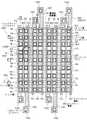
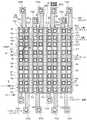
図1は、本発明に係る第1の実施形態に従ったFIN型FBCメモリの概略平面図である。FBCメモリは、SOI(Silicon On Insulator)基板上に形成される。FBCは、ソースとドレインとの間に設けられたフローティングボディFB(以下、ボディFBという)に蓄積された多数キャリアの個数によってデータ“0”またはデータ“1”を格納することができる。ソース、ドレインおよびボディFBは、SOI層に形成される。(First embodiment)
FIG. 1 is a schematic plan view of a FIN type FBC memory according to the first embodiment of the present invention. The FBC memory is formed on an SOI (Silicon On Insulator) substrate. The FBC can store data “0” or data “1” depending on the number of majority carriers accumulated in a floating body FB (hereinafter referred to as body FB) provided between the source and the drain. The source, drain and body FB are formed in the SOI layer.
本実施形態によるFBCメモリでは、2本のビット線BLが1本のソース線を共有している。ビット線BLは、ビット線コンタクトBLCを介してその下にあるドレイン(図示せず)に接続されている。ソース線SLは、ソース線コンタクトSLCを介してその下にあるソース(図2参照)に接続されている。阻止分離としてのSTI(Shallow Trench Isolation)が、隣接する2つのビット線BL間に設けられている。 In the FBC memory according to the present embodiment, two bit lines BL share one source line. The bit line BL is connected to a drain (not shown) thereunder via a bit line contact BLC. The source line SL is connected to the underlying source (see FIG. 2) via the source line contact SLC. STI (Shallow Trench Isolation) as blocking isolation is provided between two adjacent bit lines BL.
フロントゲート電極FGおよびバックゲート電極BGは、SOI層ソース線SLおよびビット線BLに対して直交するように延伸しており、隣接するボディFB間に埋め込まれている。フロントゲート電極FGは、フロントゲートコンタクトFGCと接続されている。バックゲート電極BGは、シリコン基板を介してメモリ形成領域外に設けられたバックゲートコンタクトBGCと接続されている。 The front gate electrode FG and the back gate electrode BG extend so as to be orthogonal to the SOI layer source line SL and the bit line BL, and are buried between adjacent bodies FB. The front gate electrode FG is connected to the front gate contact FGC. The back gate electrode BG is connected to a back gate contact BGC provided outside the memory formation region via a silicon substrate.
隣接するフロントゲート電極FG間には、電極間絶縁膜IEが埋め込まれている。 An interelectrode insulating film IE is buried between adjacent front gate electrodes FG.
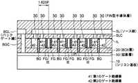
図2は、図1の2−2線に沿った断面図である。本実施形態によるFBCメモリは、シリコン基板10と、シリコン基板10上に設けられたBOX層20と、BOX層20上に設けられたFIN型半導体層30(以下、半導体層30という)とを備えている。半導体層30は、SOI基板のSOI層を用いて形成されている。半導体層30内には、ボディFBと、ボディFBの両側に設けられたソース・ドレイン領域とが設けられている。図2では、ソース領域のみが図示されている。ドレイン領域の断面は、図2に示す断面と同じ形態になるので、その図示を省略している。また、ボディFBの断面は、図2に示す断面図からソース線SL、ソース線コンタクトSLC、バックゲートコンタクトBGCおよびバックゲート線BGLを除いた形態であり、容易に推測できるので、その図示を省略する。 FIG. 2 is a cross-sectional view taken along line 2-2 of FIG. The FBC memory according to the present embodiment includes a
半導体層30の片側側面(第1の側面)には、第1のゲート絶縁膜41が形成されている。第1の側面の反対側の半導体層30の側面(第2の側面)には、第2のゲート絶縁膜42が形成されている。フロントゲート電極FGは、第1のゲート絶縁膜41を介して半導体層30の第1の側面に設けられている。隣接するフロントゲート電極FG間には、電極間絶縁膜IEが設けられている。即ち、電極間絶縁膜IEは、半導体層30の第1の側面とその半導体層30に隣接する半導体層の第1の側面との間において対向するフロントゲート電極FG間に設けられている。 A first
バックゲート電極BGは、第2のゲート絶縁膜42を介して半導体層30の第2の側面に設けられている。バックゲート電極BGは、半導体層30の第2の側面とその半導体層30に隣接する半導体層の第2の側面との間に設けられている。バックゲート電極BGは、BOX層20を貫通してシリコン基板10に達している。シリコン基板10の表面には、不純物拡散層50が設けられている。バックゲート電極BGは、拡散層50を介してバックゲートコンタクトBGCに接続されている。従って、バックゲート線BGLの電位によって、バックゲート電極BGの電位を制御することができる。 The back gate electrode BG is provided on the second side surface of the
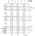
図3および図4は、本実施形態によるFIN型FBCメモリの製造方法を示す断面図である。これらの断面図は、ソース線SLに沿った断面図である。まず、図3に示すように、SOI基板を準備する。SOI基板は、シリコン基板10上にBOX層20を介して設けられた半導体層30を有する。半導体層30の膜厚は、例えば、約100nmである。半導体層30の不純物濃度は、例えば、約1×1017cm−3のP型シリコンである。この半導体層30は、そのままN型MISのチャネル領域として用いることができる。BOX層20の膜厚は、例えば、約200nmである。シリコン基板10の厚みおよびその不純物濃度は任意でよい。3 and 4 are cross-sectional views illustrating the method of manufacturing the FIN type FBC memory according to the present embodiment. These cross-sectional views are cross-sectional views along the source line SL. First, as shown in FIG. 3, an SOI substrate is prepared. The SOI substrate has a
次に、SOI基板のメモリ領域にボロンをイオン注入することによって、シリコン基板10の表面領域にP型不純物層50を形成する。このときの注入エネルギーは約130keVであり、不純物濃度は約8×1013cm−3である。続いて、半導体層30上にマスク材としてのシリコン窒化膜60を堆積する。次に、フォトリソグラフィおよびRIE(Reactive Ion Etching)を用いて、素子分離領域IA上のシリコン窒化膜60を除去する。これにより、アクティブ領域AAを被覆するハードマスクが形成される。Next, boron is ion-implanted into the memory region of the SOI substrate to form a P-
続いて、シリコン窒化膜60をマスクとして用いて、フォトリソグラフィおよびRIE(Reactive Ion Etching)で素子分離領域IAにある半導体層30を異方的にエッチングする。これにより、第1のトレンチTR1が素子分離領域IAに形成される。隣接する素子分離領域IAの間にある半導体層30はアクティブ領域AAとなる。このとき、素子分離領域IAの幅はF(Feature Size)であり、アクティブ領域AAの幅は2.25Fである。F(Feature Size)はフォトリソグラフィ技術およびエッチング技術によって形成可能な最小線幅を意味する。従って、フォトリソグラフィ技術およびエッチング技術を用いて形成可能な線幅は、全てF以上である。ただし、スペーサをマスクとして用いた場合には、F未満の線幅を実現可能である。次に、ダミー絶縁膜としてのシリコン酸化膜70を素子分離領域IAに形成されたトレンチに充填することによって、図4に示す構造が得られる。シリコン酸化膜70は、後の工程において除去されるためSTIとして残置されない。 Subsequently, using the
次に、熱燐酸溶液を用いて、シリコン窒化膜60を除去する。これにより、シリコン酸化膜70の上部側面が露出する。さらに、図5に示すように、フォトリソグラフィ技術を用いてボディ領域FBR上をフォトレジスト80で被覆する。続いて、ソース領域SRおよびドレイン領域DRにN型不純物をイオン注入する。このときのN型不純物の濃度は、約1×1015cm−3である。図5は、ソース・ドレイン形成工程における平面図である。Next, the
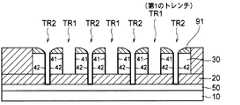
フォトレジスト80の除去後、図6に示すように、膜厚Fのシリコン窒化膜90を堆積する。続いて、RIEを用いて異方的にエッチングする。これにより、図7に示すように、シリコン窒化膜60の除去によって露出されたシリコン酸化膜70の側面に第1のスペーサ91を形成する。第1のスペーサ91の幅は、約Fである。従って、半導体層30の上面が0.25Fだけ露出される。さらに、第1のスペーサ91をマスクとして用いて、RIEで半導体層30およびBOX層20を自己整合的にエッチングする。これにより、第2のトレンチTR2が半導体層30の中間部に形成される。第2のトレンチTR2は、シリコン基板10の表面に形成された不純物拡散層50に達する。このとき、半導体層30は、細いFIN状に形成される。図8は、第2のトレンチTR2の形成後の構造を示す平面図である。図8に示すように、第2のトレンチTR2は、第1のスペーサ91およびシリコン酸化膜(ダミー絶縁膜)70に沿って延伸している。これにより、第2のトレンチTR2は、半導体層30をFIN状に分離している。 After the removal of the
次に、図8に示すように、フォトリソグラフィ技術およびエッチングを用いて、素子分離領域IAに充填されているシリコン酸化膜70を除去する。これにより、第1のトレンチTR1が再度形成される。第1および第2のトレンチTR1およびTR2の内側面では半導体層30が露出されている。この露出された半導体層30の側壁を熱酸化する。これにより、半導体層30の側面に第1のゲート絶縁膜41および第2のゲート絶縁膜42を形成する。ゲート絶縁膜41および42の膜厚は、それぞれ約6nmである。 Next, as shown in FIG. 8, the
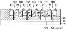
次に、ゲート絶縁膜41、42の形成時に第2のトレンチTR2の底部においてシリコン基板10上に形成されたシリコン酸化膜を除去する。続いて、図10に示すように、第1および第2のトレンチTR1およびTR2内にN型ポリシリコン120を充填する。さらに、CDE(Chemical Dry Etching)を用いてこのポリシリコン120を平坦化する。ポリシリコン120は、フロントゲート電極FGおよびバックゲート電極BGの材料となる。 Next, the silicon oxide film formed on the
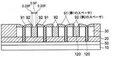
次に、膜厚0.25Fのシリコン窒化膜を堆積し、RIEを用いてこのシリコン窒化膜を異方的にエッチングする。これにより、図11に示すように、スペーサ91の側面に第2のスペーサ92を形成する。第2のスペーサ92は、第2のトレンチTR2内のポリシリコン120上に形成されている。また、このとき堆積されたシリコン窒化膜は、第1のトレンチTR1内のポリシリコン120をも被覆する。第2のスペーサ92の幅は、約0.25Fである。従って、幅0.5Fのポリシリコン120の表面が露出される。 Next, a silicon nitride film with a film thickness of 0.25F is deposited, and this silicon nitride film is anisotropically etched using RIE. Thereby, as shown in FIG. 11, the
次に、図12に示すように、第1および第2のスペーサ91および92をマスクとして用いて、RIEで第2のトレンチTR2内のポリシリコン120をBOX層20上までエッチングする。これにより、第3のトレンチTR3がポリシリコン120内に自己整合的に形成される。このとき、幅0.25Fのフロントゲート電極FGおよび幅0.25Fのバックゲート電極BGが形成される。 Next, as shown in FIG. 12, using the first and
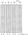
次に、図13に示すように、フォトリソグラフィおよびRIEを用いてメモリセル領域の外部のポリシリコン120を配線加工する。フロントゲート電極FGは、ポリシリコン120によってフロントゲート電極FGの延伸方向に引き伸ばされており、フロントゲートコンタクトFGCに接続されている。図13は、ポリシリコン120の配線加工後の平面図である。続いて、1000℃以上の高温アニールによって、ソース、ドレインおよび拡散層50内の不純物を活性化させる。 Next, as shown in FIG. 13, the
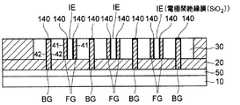
次に、チタン膜を約20nm堆積した後に、熱処理により、チタン膜とフロントゲート電極FGの側面とを反応させる。これにより、チタンポリサイド140がフロントゲート電極FGの側面に形成される。これと同時に、バックゲート電極BG上にもチタンポリサイド140が形成される。チタンポリサイド140により、フロントゲート電極FGおよびバックゲート電極BGが低抵抗化される。 Next, after depositing a titanium film with a thickness of about 20 nm, the titanium film and the side surface of the front gate electrode FG are reacted by heat treatment. Thereby, the
次に、熱燐酸溶液を用いて、第1および第2のスペーサ(SiN)91および92を除去する。次に、シリコン酸化膜を300nm以上堆積し、これをCMP等によりフロントゲート電極FGの上面が露出するまでエッチバックする。これにより、図15に示すように、第3のトレンチTR3内に電極間絶縁膜IEが形成される。 Next, the first and second spacers (SiN) 91 and 92 are removed using a hot phosphoric acid solution. Next, a silicon oxide film of 300 nm or more is deposited, and this is etched back by CMP or the like until the upper surface of the front gate electrode FG is exposed. As a result, as shown in FIG. 15, an interelectrode insulating film IE is formed in the third trench TR3.
次に、フォトリソグラフィおよびRIEを用いて、図16に示すように、半導体層30内の素子分離領域に開口160を設ける。開口160の幅は、半導体層30の幅よりも狭く形成されている。続いて、CDEを用いて、この開口160をフロントゲート電極FGおよびバックゲート電極BGに達するまでエッチングする。これにより、図17に示すように、フロントゲート電極FGおよびバックゲート電極BGを削ることなく、素子分離領域の半導体層30をエッチングすることができる。続いて、シリコン酸化膜を約300nm堆積する。このシリコン酸化膜をCMP等でエッチバックすることによって、STIが、隣接するビット線コンタクトの間に形成される。 Next, using photolithography and RIE, an
次に、層間絶縁膜ILを堆積した後、図1および図2に示すようにソース線コンタクトSLC、ビット線コンタクトBLC(図2では図示せず)、バックゲートコンタクトBGCを形成する。また、フロントゲートコンタクトFGCは、図1に示すように、ポリシリコン120からなる配線上に形成される。さらに、ソース線SL、ビット線BL、バックゲート線BGL、フロントゲート線(図示せず)等を形成する。このようにして、FIN型FBCメモリが完成する。 Next, after depositing the interlayer insulating film IL, as shown in FIGS. 1 and 2, a source line contact SLC, a bit line contact BLC (not shown in FIG. 2), and a back gate contact BGC are formed. Further, the front gate contact FGC is formed on a wiring made of
本実施形態によれば、バックゲート電極BG、フロントゲート電極FGおよび電極間絶縁膜IEは、全て自己整合的に形成され得る。これにより、バックゲート電極BG、フロントゲート電極FGおよび電極間絶縁膜IEのそれぞれの幅(ビット線BLの延伸方向の幅)は、いずれもF以下である。本実施形態では、バックゲート電極BG、フロントゲート電極FGおよび電極間絶縁膜IEのそれぞれの幅は、0.25F、0.25Fおよび0.5Fである。半導体層30の幅はFである。バックゲート電極BGおよび電極間絶縁膜IEは隣接するメモリセルと共有されている。従って、1メモリセルの幅は、0.25F/2+0.25F+0.5F/2+F=1.625Fとなる。 According to this embodiment, the back gate electrode BG, the front gate electrode FG, and the interelectrode insulating film IE can all be formed in a self-aligned manner. As a result, each of the back gate electrode BG, the front gate electrode FG, and the interelectrode insulating film IE (the width in the extending direction of the bit line BL) is F or less. In the present embodiment, the respective widths of the back gate electrode BG, the front gate electrode FG, and the interelectrode insulating film IE are 0.25F, 0.25F, and 0.5F. The width of the
ドレインの長さ(ゲート電極FG、BGの延伸方向の長さ)はF、ボディの長さはF、ソースの長さはF、並びにSTIの長さはFである。ソースおよびSTIは、隣接するメモリセルと共有されている。従って、1メモリセルの長さは、F+F+F/2+F/2=3Fとなる。よって、1つのFBCのサイズ(面積)は、図1に示すように1.625F×3F=4.875F2となる。The drain length (the length of the gate electrodes FG and BG in the extending direction) is F, the body length is F, the source length is F, and the STI length is F. The source and STI are shared with adjacent memory cells. Therefore, the length of one memory cell is F + F + F / 2 + F / 2 = 3F. Therefore, the size (area) of one FBC is 1.625F × 3F = 4.875F2 as shown in FIG.
従来、バックゲート電極BGおよびフロントゲート電極FGのそれぞれの幅がF以上であったので、1つのFBCのサイズ(面積)は、3F×3F=9F2以上であった。さらに、電気的に活性化されないシリコン部分がフロントゲート電極FG間にあったため、装置の微細化の妨げとなっていた。Conventionally, since the width of each of the back gate electrode BG and the front gate electrode FG is F or more, the size (area) of one FBC is 3F × 3F = 9F2 or more. Furthermore, since there is a silicon portion that is not electrically activated between the front gate electrodes FG, it has hindered miniaturization of the device.
本実施形態によれば、シリコン部分に代わり、フロントゲート電極FG間には、電極間絶縁膜IEが設けられている。これにより、隣接するフロントゲート電極FG間の幅を狭くすることができ、尚且つ、バックゲート電極BG、および電極間絶縁膜IEのそれぞれの幅は、F未満(0.25F、0.25Fおよび0.5F)である。従って、本実施形態では、1つのFBCのサイズを上述のように4.875F2とすることができる。本実施形態によるFIN型FBCメモリの面積は、従来のFIN型FBCメモリの面積の約54%である。このように本実施形態は、バックゲート電極BG、フロントゲート電極FGおよび電極間絶縁膜IEのそれぞれの幅をF以下にすることによってメモリ領域の微細化を可能とする。According to the present embodiment, the interelectrode insulating film IE is provided between the front gate electrodes FG instead of the silicon portion. Thereby, the width between the adjacent front gate electrodes FG can be narrowed, and the width of each of the back gate electrode BG and the interelectrode insulating film IE is less than F (0.25F, 0.25F and 0.5F). Therefore, in this embodiment, the size of one FBC can be set to 4.875F2 as described above. The area of the FIN type FBC memory according to the present embodiment is about 54% of the area of the conventional FIN type FBC memory. As described above, in the present embodiment, the memory region can be miniaturized by setting the widths of the back gate electrode BG, the front gate electrode FG, and the interelectrode insulating film IE to F or less.
本実施形態では、バックゲート電極BG、フロントゲート電極FGおよび電極間絶縁膜IEのそれぞれの幅は、いずれもF未満である。しかし、バックゲート電極BG、フロントゲート電極FGまたは電極間絶縁膜IEのいずれかの幅をF未満に形成してもよい。この場合、メモリ領域の微細化の度合いは低下するものの、FBCの面積を9F2にすることができるという効果は失われない。In the present embodiment, the respective widths of the back gate electrode BG, the front gate electrode FG, and the interelectrode insulating film IE are less than F. However, the width of any of the back gate electrode BG, the front gate electrode FG, and the interelectrode insulating film IE may be formed to be less than F. In this case, although the degree of miniaturization of the memory area is reduced, the effect that the area of the FBC can be 9F2 is not lost.
(第2の実施形態)
図18は、第2の実施形態に従ったFIN型FBCメモリの概略平面図である。第2の実施形態では、バックゲート電極BGは、シリコン基板10に接続されておらず、BOX層20上に設けられている。従って、バックゲート電極BGは、ポリシリコン120によってバックゲート電極BGの延伸方向に引き伸ばされており、フロントゲートコンタクトFGCと同じ層に形成されたバックゲートコンタクトBGCに接続されている。(Second Embodiment)
FIG. 18 is a schematic plan view of a FIN type FBC memory according to the second embodiment. In the second embodiment, the back gate electrode BG is not connected to the
図19は、図18に示す19−19線に沿った断面図である。バックゲート電極BGは、BOX層20を貫通せず、BOX層20上に設けられている。第2の実施形態のその他の構成は、第1の実施形態の構成と同様でよい。 FIG. 19 is a cross-sectional view taken along line 19-19 shown in FIG. The back gate electrode BG is provided on the
第2の実施形態によるFBCメモリの製造方法と第1の実施形態によるFBCメモリの製造方法との相違点を説明する。第2の実施形態によるFBCメモリでは、図7に示す第2のトレンチTR2形成工程において、半導体層30のエッチングをBOX層20の上面で停止させる。 Differences between the FBC memory manufacturing method according to the second embodiment and the FBC memory manufacturing method according to the first embodiment will be described. In the FBC memory according to the second embodiment, the etching of the
図13に示すポリシリコン120の加工工程では、フロントゲート電極FGだけでなくバックゲート電極BGについても、メモリセル領域の外部のポリシリコン120を配線加工する。これにより、フロントゲート電極FGおよびバックゲート電極BGの両方は、ポリシリコン120によってそれらの延伸方向に引き伸ばされる。第2の実施形態によるFBCメモリのその他の製造工程は、第1の実施形態によるFBCメモリの製造工程と同一である。 In the processing step of the
第2の実施形態では、第2のトレンチをシリコン基板10に達するほど深く形成する必要が無い。第2の実施形態は、シリコン基板10に達する深いバックゲートコンタクトBGCを形成する必要が無い。また、拡散層50を形成する必要が無い。従って、第2の実施形態によるFBCメモリは、製造することが比較的容易である。さらに、第2の実施形態は、第1の実施形態と同様の効果を得ることができる。 In the second embodiment, it is not necessary to form the second trench deep enough to reach the
10・・・シリコン基板
20・・・BOX層
30・・・FIN型半導体層
41・・・第1のゲート絶縁膜
42・・・第2のゲート絶縁膜
50・・・拡散層
FG・・・フロントゲート電極
BG・・・バックゲート電極
IE・・・電極間絶縁膜
BL・・・ビット線
SL・・・ソース線
BLC・・・ビット線コンタクト
SLC・・・ソース線コンタクトDESCRIPTION OF
Claims (5)
Translated fromJapanese前記半導体基板上に設けられた絶縁層と、
前記絶縁層上に設けられ、電気的に浮遊状態のフローティングボディ領域、および、該フローティングボディ領域の両側にあるソース・ドレイン領域を含む複数のFIN型半導体層と、
前記FIN型半導体層の第1の側面に設けられた第1のゲート絶縁膜と、
前記第1の側面の反対側の前記FIN型半導体層の第2の側面に設けられた第2のゲート絶縁膜と、
前記第1の側面に前記第1のゲート絶縁膜を介して設けられたフロントゲート電極と、
或るFIN型半導体層の第2の側面と該第2の側面側に隣接する他のFIN型半導体層の第2の側面との間に設けられたバックゲート電極とを備え、
設計可能な最小線幅をFとした場合に、前記フロントゲート電極または前記バックゲート絶縁膜のいずれかの幅がF未満であることを特徴とする半導体記憶装置。A semiconductor substrate;
An insulating layer provided on the semiconductor substrate;
A plurality of FIN type semiconductor layers provided on the insulating layer and including a floating body region in an electrically floating state and source / drain regions on both sides of the floating body region;
A first gate insulating film provided on a first side surface of the FIN-type semiconductor layer;
A second gate insulating film provided on a second side surface of the FIN-type semiconductor layer opposite to the first side surface;
A front gate electrode provided on the first side surface via the first gate insulating film;
A back gate electrode provided between a second side surface of a certain FIN type semiconductor layer and a second side surface of another FIN type semiconductor layer adjacent to the second side surface;
A semiconductor memory device, wherein the width of either the front gate electrode or the back gate insulating film is less than F, where F is the minimum line width that can be designed.
前記拡散層に接続され、メモリ形成領域外に設けられたバックゲートコンタクトとをさらに備え、
前記バックゲート電極は、前記絶縁膜を貫通して前記拡散層に接続され、該拡散層を介して前記バックゲートコンタクトに接続されていることを特徴とする請求項1に記載の半導体記憶装置。A diffusion layer formed on the surface of the semiconductor substrate;
A back gate contact connected to the diffusion layer and provided outside the memory formation region;
The semiconductor memory device according to claim 1, wherein the back gate electrode is connected to the diffusion layer through the insulating film, and is connected to the back gate contact through the diffusion layer.
前記電極間絶縁膜の幅が前記F未満であることを特徴とする請求項1または請求項2に記載の半導体記憶装置。Inter-electrode insulation provided between the front gate electrodes facing each other between the first side surface of a certain FIN type semiconductor layer and the first side surface of another FIN type semiconductor layer adjacent to the first side surface side And further comprising a membrane,
The semiconductor memory device according to claim 1, wherein a width of the interelectrode insulating film is less than the F.
前記半導体層上にアクティブエリアを被覆するマスク材を形成し、
前記マスク材を用いて、前記半導体層の素子分離領域をエッチングして第1のトレンチを形成し、
前記第1のトレンチにダミー絶縁膜を充填し、
前記マスク材を除去し、
前記マスク材の除去によって露出された前記ダミー絶縁膜の側面に第1のスペーサを形成し、
前記第1のスペーサをマスクとして用いて、前記アクティブエリアに第2のトレンチを形成し、
前記ダミー絶縁膜を除去することによって前記第1のトレンチを再度形成し、
前記第1および前記第2のトレンチによって規定されたFIN型半導体層の側面にそれぞれ第1および第2のゲート絶縁膜を形成し、
前記第1および前記第2のトレンチにそれぞれフロントゲート電極およびバックゲート電極の材料としてのポリシリコンを充填することを具備した半導体記憶装置の製造方法。Preparing a substrate having a semiconductor layer provided via an insulating film on the semiconductor substrate;
Forming a mask material covering the active area on the semiconductor layer;
Using the mask material, the element isolation region of the semiconductor layer is etched to form a first trench,
Filling the first trench with a dummy insulating film;
Removing the mask material;
Forming a first spacer on a side surface of the dummy insulating film exposed by removing the mask material;
Forming a second trench in the active area using the first spacer as a mask;
Forming the first trench again by removing the dummy insulating film;
Forming first and second gate insulating films on side surfaces of the FIN type semiconductor layer defined by the first and second trenches, respectively;
A method of manufacturing a semiconductor memory device, comprising filling the first and second trenches with polysilicon as a material for a front gate electrode and a back gate electrode, respectively.
前記第2のトレンチ内のポリシリコン上において前記第1のスペーサの側面に第2のスペーサを形成し、
前記第2のスペーサをマスクとして用いて、前記第2のトレンチ内のポリシリコンを前記絶縁膜上までエッチングすることによって、前記第2のトレンチ内のポリシリコンに第3のトレンチを形成し、
前記第3のトレンチ内に電極間絶縁膜を充填することをさらに具備したことを特徴とする請求項4に記載の半導体記憶装置の製造方法。The second trench is formed to reach the semiconductor substrate;
Forming a second spacer on a side surface of the first spacer on the polysilicon in the second trench;
Forming a third trench in the polysilicon in the second trench by etching the polysilicon in the second trench to the top of the insulating film using the second spacer as a mask;
The method of manufacturing a semiconductor memory device according to claim 4, further comprising filling an interelectrode insulating film in the third trench.
Priority Applications (2)
| Application Number | Priority Date | Filing Date | Title |
|---|---|---|---|
| JP2006177009AJP2008010503A (en) | 2006-06-27 | 2006-06-27 | Semiconductor memory device and manufacturing method thereof |
| US11/760,401US7629651B2 (en) | 2006-06-27 | 2007-06-08 | Semiconductor memory device and manufacturing method therefor |
Applications Claiming Priority (1)
| Application Number | Priority Date | Filing Date | Title |
|---|---|---|---|
| JP2006177009AJP2008010503A (en) | 2006-06-27 | 2006-06-27 | Semiconductor memory device and manufacturing method thereof |
Publications (1)
| Publication Number | Publication Date |
|---|---|
| JP2008010503Atrue JP2008010503A (en) | 2008-01-17 |
Family
ID=38872767
Family Applications (1)
| Application Number | Title | Priority Date | Filing Date |
|---|---|---|---|
| JP2006177009APendingJP2008010503A (en) | 2006-06-27 | 2006-06-27 | Semiconductor memory device and manufacturing method thereof |
Country Status (2)
| Country | Link |
|---|---|
| US (1) | US7629651B2 (en) |
| JP (1) | JP2008010503A (en) |
Cited By (9)
| Publication number | Priority date | Publication date | Assignee | Title |
|---|---|---|---|---|
| JP2013521651A (en)* | 2010-03-02 | 2013-06-10 | マイクロン テクノロジー, インク. | Floating body cell, device including floating body cell, and method for forming floating body cell. |
| US8809145B2 (en) | 2010-03-02 | 2014-08-19 | Micron Technology, Inc. | Semiconductor cells, arrays, devices and systems having a buried conductive line and methods for forming the same |
| US8980699B2 (en) | 2010-03-02 | 2015-03-17 | Micron Technology, Inc. | Thyristor-based memory cells, devices and systems including the same and methods for forming the same |
| US9129983B2 (en) | 2011-02-11 | 2015-09-08 | Micron Technology, Inc. | Memory cells, memory arrays, methods of forming memory cells, and methods of forming a shared doped semiconductor region of a vertically oriented thyristor and a vertically oriented access transistor |
| US9269795B2 (en) | 2011-07-26 | 2016-02-23 | Micron Technology, Inc. | Circuit structures, memory circuitry, and methods |
| US9361966B2 (en) | 2011-03-08 | 2016-06-07 | Micron Technology, Inc. | Thyristors |
| US9608119B2 (en) | 2010-03-02 | 2017-03-28 | Micron Technology, Inc. | Semiconductor-metal-on-insulator structures, methods of forming such structures, and semiconductor devices including such structures |
| US9646869B2 (en) | 2010-03-02 | 2017-05-09 | Micron Technology, Inc. | Semiconductor devices including a diode structure over a conductive strap and methods of forming such semiconductor devices |
| US10373956B2 (en) | 2011-03-01 | 2019-08-06 | Micron Technology, Inc. | Gated bipolar junction transistors, memory arrays, and methods of forming gated bipolar junction transistors |
Families Citing this family (14)
| Publication number | Priority date | Publication date | Assignee | Title |
|---|---|---|---|---|
| KR100843717B1 (en)* | 2007-06-28 | 2008-07-04 | 삼성전자주식회사 | Semiconductor device having floating body device and bulk body device and manufacturing method thereof |
| KR100555569B1 (en) | 2004-08-06 | 2006-03-03 | 삼성전자주식회사 | A semiconductor device having a channel region limited by an insulating film and its manufacturing method |
| FR2917896B1 (en)* | 2007-06-21 | 2009-11-06 | Commissariat Energie Atomique | FIELD EFFECT TRANSISTOR WITH ALTERNATE ELECTRICAL CONTACTS. |
| US8148776B2 (en) | 2008-09-15 | 2012-04-03 | Micron Technology, Inc. | Transistor with a passive gate |
| JP5645368B2 (en)* | 2009-04-14 | 2014-12-24 | 株式会社日立製作所 | Semiconductor device and manufacturing method thereof |
| US8664729B2 (en) | 2011-12-14 | 2014-03-04 | Taiwan Semiconductor Manufacturing Company, Ltd. | Methods and apparatus for reduced gate resistance finFET |
| KR101953240B1 (en) | 2012-09-14 | 2019-03-04 | 삼성전자 주식회사 | Fin Transistor and Semiconductor integrated circuit including the same |
| US8716094B1 (en)* | 2012-11-21 | 2014-05-06 | Global Foundries Inc. | FinFET formation using double patterning memorization |
| CN103855021B (en)* | 2012-12-04 | 2017-04-05 | 中芯国际集成电路制造(上海)有限公司 | A kind of manufacture method of FinFET |
| FR3003691B1 (en)* | 2013-03-19 | 2016-07-01 | Soitec Silicon On Insulator | FINFET WITH REAR GRILLE |
| US8703557B1 (en)* | 2013-04-15 | 2014-04-22 | Globalfoundries Inc. | Methods of removing dummy fin structures when forming finFET devices |
| US9209248B2 (en)* | 2013-08-07 | 2015-12-08 | Infineon Technologies Dresden Gmbh | Power transistor |
| CN104425601B (en)* | 2013-08-30 | 2018-02-16 | 中国科学院微电子研究所 | Semiconductor device and method for manufacturing the same |
| US9613954B2 (en) | 2014-07-08 | 2017-04-04 | International Business Machines Corporation | Selective removal of semiconductor fins |
Family Cites Families (6)
| Publication number | Priority date | Publication date | Assignee | Title |
|---|---|---|---|---|
| US6770516B2 (en)* | 2002-09-05 | 2004-08-03 | Taiwan Semiconductor Manufacturing Company | Method of forming an N channel and P channel FINFET device on the same semiconductor substrate |
| US6888199B2 (en)* | 2003-10-07 | 2005-05-03 | International Business Machines Corporation | High-density split-gate FinFET |
| US7049654B2 (en)* | 2004-03-31 | 2006-05-23 | Intel Corporation | Memory with split gate devices and method of fabrication |
| JP3964885B2 (en)* | 2004-05-19 | 2007-08-22 | 株式会社東芝 | Semiconductor device and manufacturing method thereof |
| US7564081B2 (en)* | 2005-11-30 | 2009-07-21 | International Business Machines Corporation | finFET structure with multiply stressed gate electrode |
| JP4791986B2 (en)* | 2007-03-01 | 2011-10-12 | 株式会社東芝 | Semiconductor memory device |
- 2006
- 2006-06-27JPJP2006177009Apatent/JP2008010503A/enactivePending
- 2007
- 2007-06-08USUS11/760,401patent/US7629651B2/ennot_activeExpired - Fee Related
Cited By (16)
| Publication number | Priority date | Publication date | Assignee | Title |
|---|---|---|---|---|
| US10157769B2 (en) | 2010-03-02 | 2018-12-18 | Micron Technology, Inc. | Semiconductor devices including a diode structure over a conductive strap and methods of forming such semiconductor devices |
| US9608119B2 (en) | 2010-03-02 | 2017-03-28 | Micron Technology, Inc. | Semiconductor-metal-on-insulator structures, methods of forming such structures, and semiconductor devices including such structures |
| US8841715B2 (en) | 2010-03-02 | 2014-09-23 | Micron Technology, Inc. | Floating body cell structures, devices including same, and methods for forming same |
| US8859359B2 (en) | 2010-03-02 | 2014-10-14 | Micron Technology, Inc. | Floating body cell structures, devices including same, and methods for forming same |
| US8866209B2 (en) | 2010-03-02 | 2014-10-21 | Micron Technology, Inc. | Semiconductor cells, arrays, devices and systems having a buried conductive line and methods for forming the same |
| US8980699B2 (en) | 2010-03-02 | 2015-03-17 | Micron Technology, Inc. | Thyristor-based memory cells, devices and systems including the same and methods for forming the same |
| US8809145B2 (en) | 2010-03-02 | 2014-08-19 | Micron Technology, Inc. | Semiconductor cells, arrays, devices and systems having a buried conductive line and methods for forming the same |
| US10325926B2 (en) | 2010-03-02 | 2019-06-18 | Micron Technology, Inc. | Semiconductor-metal-on-insulator structures, methods of forming such structures, and semiconductor devices including such structures |
| JP2013521651A (en)* | 2010-03-02 | 2013-06-10 | マイクロン テクノロジー, インク. | Floating body cell, device including floating body cell, and method for forming floating body cell. |
| US9646869B2 (en) | 2010-03-02 | 2017-05-09 | Micron Technology, Inc. | Semiconductor devices including a diode structure over a conductive strap and methods of forming such semiconductor devices |
| US9129983B2 (en) | 2011-02-11 | 2015-09-08 | Micron Technology, Inc. | Memory cells, memory arrays, methods of forming memory cells, and methods of forming a shared doped semiconductor region of a vertically oriented thyristor and a vertically oriented access transistor |
| US10373956B2 (en) | 2011-03-01 | 2019-08-06 | Micron Technology, Inc. | Gated bipolar junction transistors, memory arrays, and methods of forming gated bipolar junction transistors |
| US10886273B2 (en) | 2011-03-01 | 2021-01-05 | Micron Technology, Inc. | Gated bipolar junction transistors, memory arrays, and methods of forming gated bipolar junction transistors |
| US9691465B2 (en) | 2011-03-08 | 2017-06-27 | Micron Technology, Inc. | Thyristors, methods of programming thyristors, and methods of forming thyristors |
| US9361966B2 (en) | 2011-03-08 | 2016-06-07 | Micron Technology, Inc. | Thyristors |
| US9269795B2 (en) | 2011-07-26 | 2016-02-23 | Micron Technology, Inc. | Circuit structures, memory circuitry, and methods |
Also Published As
| Publication number | Publication date |
|---|---|
| US20070296014A1 (en) | 2007-12-27 |
| US7629651B2 (en) | 2009-12-08 |
Similar Documents
| Publication | Publication Date | Title |
|---|---|---|
| JP2008010503A (en) | Semiconductor memory device and manufacturing method thereof | |
| JP4031329B2 (en) | Semiconductor device and manufacturing method thereof | |
| TWI752431B (en) | Semiconductor device | |
| US7723184B2 (en) | Semiconductor device and manufacture method therefor | |
| JP4762060B2 (en) | Semiconductor memory device and manufacturing method thereof | |
| US10062581B2 (en) | Methods of forming an isolation structure and methods of manufacturing a semiconductor device including the same | |
| US7592643B2 (en) | Semiconductor device having a vertical transistor and method for manufacturing the same | |
| US8928073B2 (en) | Semiconductor devices including guard ring structures | |
| JP2006339476A (en) | Semiconductor device and manufacturing method thereof | |
| JP2004214379A (en) | Semiconductor device, dynamic semiconductor memory device, and method of manufacturing semiconductor device | |
| TW200843111A (en) | Floating body memory cell having gates favoring different conductivity type regions | |
| TW201133842A (en) | Semiconductor device and method of making the same | |
| CN108140669A (en) | Non-volatile separate gate storage unit with integrated high-K metal gate and preparation method thereof | |
| US10109634B2 (en) | Semiconductor device having air gap and method for manufacturing the same, memory cell having the same and electronic device having the same | |
| JP2012174790A (en) | Semiconductor device and manufacturing method of the same | |
| JP2009224520A (en) | Semiconductor device and method of manufacturing semiconductor device | |
| JP2008124189A (en) | Semiconductor device and manufacturing method thereof | |
| JP2009016760A (en) | Semiconductor memory device | |
| JP5736808B2 (en) | Semiconductor device and manufacturing method thereof | |
| JP4080485B2 (en) | Bit line structure and manufacturing method thereof | |
| US8748978B2 (en) | Sense-amp transistor of semiconductor device and method for manufacturing the same | |
| JP2013069770A (en) | Semiconductor device and manufacturing method of the same | |
| JP2008053274A (en) | Semiconductor device and manufacturing method thereof | |
| JP2011066052A (en) | Semiconductor device manufacturing method, and the semiconductor device | |
| JP2008288567A (en) | Semiconductor memory device and manufacturing method thereof |