JP2007536101A - Nanofiber array capillary lithography - Google Patents
Nanofiber array capillary lithographyDownload PDFInfo
- Publication number
- JP2007536101A JP2007536101AJP2007511622AJP2007511622AJP2007536101AJP 2007536101 AJP2007536101 AJP 2007536101AJP 2007511622 AJP2007511622 AJP 2007511622AJP 2007511622 AJP2007511622 AJP 2007511622AJP 2007536101 AJP2007536101 AJP 2007536101A
- Authority
- JP
- Japan
- Prior art keywords
- liquid
- substrate
- nanofeature
- nanofeatures
- nanostructure
- Prior art date
- Legal status (The legal status is an assumption and is not a legal conclusion. Google has not performed a legal analysis and makes no representation as to the accuracy of the status listed.)
- Pending
Links
- 238000001459lithographyMethods0.000titleabstractdescription4
- 239000002121nanofiberSubstances0.000titledescription5
- 238000000034methodMethods0.000claimsabstractdescription103
- 239000002086nanomaterialSubstances0.000claimsabstractdescription102
- 239000000758substrateSubstances0.000claimsabstractdescription63
- 239000007788liquidSubstances0.000claimsabstractdescription54
- 230000008020evaporationEffects0.000claimsabstractdescription5
- 238000001704evaporationMethods0.000claimsabstractdescription5
- 239000002071nanotubeSubstances0.000claimsdescription37
- 239000000463materialSubstances0.000claimsdescription21
- 230000008569processEffects0.000claimsdescription18
- 238000000059patterningMethods0.000claimsdescription11
- CSCPPACGZOOCGX-UHFFFAOYSA-NAcetoneChemical compoundCC(C)=OCSCPPACGZOOCGX-UHFFFAOYSA-N0.000claimsdescription8
- 238000005229chemical vapour depositionMethods0.000claimsdescription8
- 239000002245particleSubstances0.000claimsdescription7
- 229920000642polymerPolymers0.000claimsdescription6
- XLYOFNOQVPJJNP-UHFFFAOYSA-NwaterSubstancesOXLYOFNOQVPJJNP-UHFFFAOYSA-N0.000claimsdescription6
- 239000000853adhesiveSubstances0.000claimsdescription5
- 230000001070adhesive effectEffects0.000claimsdescription5
- 239000000725suspensionSubstances0.000claimsdescription4
- 239000004793PolystyreneSubstances0.000claimsdescription2
- 239000011859microparticleSubstances0.000claimsdescription2
- 239000000203mixtureSubstances0.000claimsdescription2
- 229920002223polystyrenePolymers0.000claimsdescription2
- OKKJLVBELUTLKV-UHFFFAOYSA-NMethanolChemical compoundOCOKKJLVBELUTLKV-UHFFFAOYSA-N0.000claims3
- 230000003247decreasing effectEffects0.000claims3
- 239000004205dimethyl polysiloxaneSubstances0.000claims3
- 235000013870dimethyl polysiloxaneNutrition0.000claims3
- CXQXSVUQTKDNFP-UHFFFAOYSA-NoctamethyltrisiloxaneChemical compoundC[Si](C)(C)O[Si](C)(C)O[Si](C)(C)CCXQXSVUQTKDNFP-UHFFFAOYSA-N0.000claims3
- 238000004987plasma desorption mass spectroscopyMethods0.000claims3
- 229920000435poly(dimethylsiloxane)Polymers0.000claims3
- 125000004432carbon atomChemical groupC*0.000claims1
- 238000004132cross linkingMethods0.000claims1
- 239000003960organic solventSubstances0.000claims1
- 239000002861polymer materialSubstances0.000claims1
- 239000011257shell materialSubstances0.000claims1
- 230000003075superhydrophobic effectEffects0.000claims1
- OKTJSMMVPCPJKN-UHFFFAOYSA-NCarbonChemical compound[C]OKTJSMMVPCPJKN-UHFFFAOYSA-N0.000abstractdescription21
- 239000002041carbon nanotubeSubstances0.000abstractdescription19
- 229910021393carbon nanotubeInorganic materials0.000abstractdescription19
- 239000000835fiberSubstances0.000abstractdescription6
- 238000009792diffusion processMethods0.000abstract1
- 238000001035dryingMethods0.000description19
- 230000015572biosynthetic processEffects0.000description14
- 238000005755formation reactionMethods0.000description14
- 238000001000micrographMethods0.000description11
- PXHVJJICTQNCMI-UHFFFAOYSA-NNickelChemical compound[Ni]PXHVJJICTQNCMI-UHFFFAOYSA-N0.000description9
- 239000003054catalystSubstances0.000description7
- 230000003197catalytic effectEffects0.000description7
- 239000012530fluidSubstances0.000description7
- 238000009736wettingMethods0.000description7
- 229910052751metalInorganic materials0.000description6
- 239000002184metalSubstances0.000description6
- 230000008859changeEffects0.000description5
- 229910052759nickelInorganic materials0.000description5
- XUIMIQQOPSSXEZ-UHFFFAOYSA-NSiliconChemical compound[Si]XUIMIQQOPSSXEZ-UHFFFAOYSA-N0.000description4
- 238000005516engineering processMethods0.000description4
- 239000011521glassSubstances0.000description4
- 230000003993interactionEffects0.000description4
- 229910052710siliconInorganic materials0.000description4
- 239000010703siliconSubstances0.000description4
- 239000002109single walled nanotubeSubstances0.000description4
- XEEYBQQBJWHFJM-UHFFFAOYSA-NIronChemical compound[Fe]XEEYBQQBJWHFJM-UHFFFAOYSA-N0.000description3
- VYPSYNLAJGMNEJ-UHFFFAOYSA-NSilicium dioxideChemical compoundO=[Si]=OVYPSYNLAJGMNEJ-UHFFFAOYSA-N0.000description3
- 238000010586diagramMethods0.000description3
- 230000000694effectsEffects0.000description3
- 239000011344liquid materialSubstances0.000description3
- 239000002904solventSubstances0.000description3
- QGZKDVFQNNGYKY-UHFFFAOYSA-NAmmoniaChemical compoundNQGZKDVFQNNGYKY-UHFFFAOYSA-N0.000description2
- XKRFYHLGVUSROY-UHFFFAOYSA-NArgonChemical compound[Ar]XKRFYHLGVUSROY-UHFFFAOYSA-N0.000description2
- IJGRMHOSHXDMSA-UHFFFAOYSA-NAtomic nitrogenChemical compoundN#NIJGRMHOSHXDMSA-UHFFFAOYSA-N0.000description2
- LFQSCWFLJHTTHZ-UHFFFAOYSA-NEthanolChemical compoundCCOLFQSCWFLJHTTHZ-UHFFFAOYSA-N0.000description2
- VGGSQFUCUMXWEO-UHFFFAOYSA-NEtheneChemical compoundC=CVGGSQFUCUMXWEO-UHFFFAOYSA-N0.000description2
- 239000005977EthyleneSubstances0.000description2
- 238000005411Van der Waals forceMethods0.000description2
- 230000004888barrier functionEffects0.000description2
- 150000001875compoundsChemical class0.000description2
- 238000010276constructionMethods0.000description2
- 238000013461designMethods0.000description2
- 239000006185dispersionSubstances0.000description2
- 238000009826distributionMethods0.000description2
- 238000000609electron-beam lithographyMethods0.000description2
- 230000005484gravityEffects0.000description2
- 230000002209hydrophobic effectEffects0.000description2
- 238000004519manufacturing processMethods0.000description2
- VNWKTOKETHGBQD-UHFFFAOYSA-NmethaneChemical compoundCVNWKTOKETHGBQD-UHFFFAOYSA-N0.000description2
- 230000006911nucleationEffects0.000description2
- 238000010899nucleationMethods0.000description2
- TWNQGVIAIRXVLR-UHFFFAOYSA-Noxo(oxoalumanyloxy)alumaneChemical compoundO=[Al]O[Al]=OTWNQGVIAIRXVLR-UHFFFAOYSA-N0.000description2
- 230000008707rearrangementEffects0.000description2
- 238000001338self-assemblyMethods0.000description2
- 235000012239silicon dioxideNutrition0.000description2
- 239000007787solidSubstances0.000description2
- 238000012360testing methodMethods0.000description2
- 230000037303wrinklesEffects0.000description2
- 1250000038212-(trimethylsilyl)ethoxymethyl groupChemical group[H]C([H])([H])[Si](C([H])([H])[H])(C([H])([H])[H])C([H])([H])C(OC([H])([H])[*])([H])[H]0.000description1
- UGFAIRIUMAVXCW-UHFFFAOYSA-NCarbon monoxideChemical compound[O+]#[C-]UGFAIRIUMAVXCW-UHFFFAOYSA-N0.000description1
- 229910017709Ni CoInorganic materials0.000description1
- 229910000990Ni alloyInorganic materials0.000description1
- 229910003267Ni-CoInorganic materials0.000description1
- 229910003262Ni‐CoInorganic materials0.000description1
- 229910004298SiO 2Inorganic materials0.000description1
- XOLBLPGZBRYERU-UHFFFAOYSA-NSnO2Inorganic materialsO=[Sn]=OXOLBLPGZBRYERU-UHFFFAOYSA-N0.000description1
- 229910001069Ti alloyInorganic materials0.000description1
- ATJFFYVFTNAWJD-UHFFFAOYSA-NTinChemical compound[Sn]ATJFFYVFTNAWJD-UHFFFAOYSA-N0.000description1
- 230000009471actionEffects0.000description1
- 230000004913activationEffects0.000description1
- 229910045601alloyInorganic materials0.000description1
- 239000000956alloySubstances0.000description1
- PNEYBMLMFCGWSK-UHFFFAOYSA-Naluminium oxideInorganic materials[O-2].[O-2].[O-2].[Al+3].[Al+3]PNEYBMLMFCGWSK-UHFFFAOYSA-N0.000description1
- 229910021529ammoniaInorganic materials0.000description1
- 229910021486amorphous silicon dioxideInorganic materials0.000description1
- 238000004458analytical methodMethods0.000description1
- 230000003466anti-cipated effectEffects0.000description1
- 229910052786argonInorganic materials0.000description1
- 238000003491arrayMethods0.000description1
- 210000004666bacterial sporeAnatomy0.000description1
- 238000005452bendingMethods0.000description1
- 229910002091carbon monoxideInorganic materials0.000description1
- 238000003889chemical engineeringMethods0.000description1
- 125000003636chemical groupChemical group0.000description1
- 229910017052cobaltInorganic materials0.000description1
- 239000010941cobaltSubstances0.000description1
- GUTLYIVDDKVIGB-UHFFFAOYSA-Ncobalt atomChemical compound[Co]GUTLYIVDDKVIGB-UHFFFAOYSA-N0.000description1
- GVPFVAHMJGGAJG-UHFFFAOYSA-Lcobalt dichlorideChemical compound[Cl-].[Cl-].[Co+2]GVPFVAHMJGGAJG-UHFFFAOYSA-L0.000description1
- 230000006378damageEffects0.000description1
- 238000000151depositionMethods0.000description1
- 230000008021depositionEffects0.000description1
- 238000001514detection methodMethods0.000description1
- 229940117927ethylene oxideDrugs0.000description1
- 238000007667floatingMethods0.000description1
- 229910002804graphiteInorganic materials0.000description1
- 239000010439graphiteSubstances0.000description1
- 239000001257hydrogenSubstances0.000description1
- 229910052739hydrogenInorganic materials0.000description1
- 125000004435hydrogen atomChemical class[H]*0.000description1
- 230000005661hydrophobic surfaceEffects0.000description1
- 238000003384imaging methodMethods0.000description1
- 230000010354integrationEffects0.000description1
- 229910052742ironInorganic materials0.000description1
- MVFCKEFYUDZOCX-UHFFFAOYSA-Niron(2+);dinitrateChemical compound[Fe+2].[O-][N+]([O-])=O.[O-][N+]([O-])=OMVFCKEFYUDZOCX-UHFFFAOYSA-N0.000description1
- 230000001788irregularEffects0.000description1
- 238000000608laser ablationMethods0.000description1
- 238000005259measurementMethods0.000description1
- 150000002739metalsChemical class0.000description1
- 239000000693micelleSubstances0.000description1
- 238000005459micromachiningMethods0.000description1
- 150000002815nickelChemical class0.000description1
- 229910052757nitrogenInorganic materials0.000description1
- 238000012856packingMethods0.000description1
- 230000000149penetrating effectEffects0.000description1
- 238000005268plasma chemical vapour depositionMethods0.000description1
- 239000000843powderSubstances0.000description1
- 238000012545processingMethods0.000description1
- 102000004169proteins and genesHuman genes0.000description1
- 108090000623proteins and genesProteins0.000description1
- 238000000197pyrolysisMethods0.000description1
- 239000010453quartzSubstances0.000description1
- 230000004044responseEffects0.000description1
- 229910052594sapphireInorganic materials0.000description1
- 239000010980sapphireSubstances0.000description1
- 238000001878scanning electron micrographMethods0.000description1
- 238000004626scanning electron microscopyMethods0.000description1
- 238000000926separation methodMethods0.000description1
- 239000000377silicon dioxideSubstances0.000description1
- 239000012798spherical particleSubstances0.000description1
- 238000005728strengtheningMethods0.000description1
- 239000004094surface-active agentSubstances0.000description1
- 238000005979thermal decomposition reactionMethods0.000description1
- 229940054870ursoDrugs0.000description1
- 238000009423ventilationMethods0.000description1
- 235000012431wafersNutrition0.000description1
Images


Classifications
- B—PERFORMING OPERATIONS; TRANSPORTING
- B82—NANOTECHNOLOGY
- B82B—NANOSTRUCTURES FORMED BY MANIPULATION OF INDIVIDUAL ATOMS, MOLECULES, OR LIMITED COLLECTIONS OF ATOMS OR MOLECULES AS DISCRETE UNITS; MANUFACTURE OR TREATMENT THEREOF
- B82B3/00—Manufacture or treatment of nanostructures by manipulation of individual atoms or molecules, or limited collections of atoms or molecules as discrete units
- B—PERFORMING OPERATIONS; TRANSPORTING
- B82—NANOTECHNOLOGY
- B82Y—SPECIFIC USES OR APPLICATIONS OF NANOSTRUCTURES; MEASUREMENT OR ANALYSIS OF NANOSTRUCTURES; MANUFACTURE OR TREATMENT OF NANOSTRUCTURES
- B82Y10/00—Nanotechnology for information processing, storage or transmission, e.g. quantum computing or single electron logic
- B—PERFORMING OPERATIONS; TRANSPORTING
- B82—NANOTECHNOLOGY
- B82Y—SPECIFIC USES OR APPLICATIONS OF NANOSTRUCTURES; MEASUREMENT OR ANALYSIS OF NANOSTRUCTURES; MANUFACTURE OR TREATMENT OF NANOSTRUCTURES
- B82Y30/00—Nanotechnology for materials or surface science, e.g. nanocomposites
- B—PERFORMING OPERATIONS; TRANSPORTING
- B82—NANOTECHNOLOGY
- B82Y—SPECIFIC USES OR APPLICATIONS OF NANOSTRUCTURES; MEASUREMENT OR ANALYSIS OF NANOSTRUCTURES; MANUFACTURE OR TREATMENT OF NANOSTRUCTURES
- B82Y40/00—Manufacture or treatment of nanostructures
- H—ELECTRICITY
- H01—ELECTRIC ELEMENTS
- H01J—ELECTRIC DISCHARGE TUBES OR DISCHARGE LAMPS
- H01J9/00—Apparatus or processes specially adapted for the manufacture, installation, removal, maintenance of electric discharge tubes, discharge lamps, or parts thereof; Recovery of material from discharge tubes or lamps
- H01J9/02—Manufacture of electrodes or electrode systems
- H01J9/022—Manufacture of electrodes or electrode systems of cold cathodes
- H01J9/025—Manufacture of electrodes or electrode systems of cold cathodes of field emission cathodes
- H—ELECTRICITY
- H01—ELECTRIC ELEMENTS
- H01J—ELECTRIC DISCHARGE TUBES OR DISCHARGE LAMPS
- H01J2201/00—Electrodes common to discharge tubes
- H01J2201/30—Cold cathodes
- H01J2201/304—Field emission cathodes
- H01J2201/30446—Field emission cathodes characterised by the emitter material
- H01J2201/30453—Carbon types
- H01J2201/30469—Carbon nanotubes (CNTs)
- H—ELECTRICITY
- H01—ELECTRIC ELEMENTS
- H01J—ELECTRIC DISCHARGE TUBES OR DISCHARGE LAMPS
- H01J2329/00—Electron emission display panels, e.g. field emission display panels
- Y—GENERAL TAGGING OF NEW TECHNOLOGICAL DEVELOPMENTS; GENERAL TAGGING OF CROSS-SECTIONAL TECHNOLOGIES SPANNING OVER SEVERAL SECTIONS OF THE IPC; TECHNICAL SUBJECTS COVERED BY FORMER USPC CROSS-REFERENCE ART COLLECTIONS [XRACs] AND DIGESTS
- Y10—TECHNICAL SUBJECTS COVERED BY FORMER USPC
- Y10S—TECHNICAL SUBJECTS COVERED BY FORMER USPC CROSS-REFERENCE ART COLLECTIONS [XRACs] AND DIGESTS
- Y10S977/00—Nanotechnology
- Y10S977/70—Nanostructure
- Y10S977/734—Fullerenes, i.e. graphene-based structures, such as nanohorns, nanococoons, nanoscrolls or fullerene-like structures, e.g. WS2 or MoS2 chalcogenide nanotubes, planar C3N4, etc.
- Y10S977/742—Carbon nanotubes, CNTs
Landscapes
- Engineering & Computer Science (AREA)
- Chemical & Material Sciences (AREA)
- Nanotechnology (AREA)
- Crystallography & Structural Chemistry (AREA)
- Physics & Mathematics (AREA)
- Manufacturing & Machinery (AREA)
- General Physics & Mathematics (AREA)
- Condensed Matter Physics & Semiconductors (AREA)
- Composite Materials (AREA)
- Materials Engineering (AREA)
- Mathematical Physics (AREA)
- Theoretical Computer Science (AREA)
- Carbon And Carbon Compounds (AREA)
Abstract
Translated fromJapaneseDescription
Translated fromJapanese 本発明はナノスケールの対象物からなる群の制御されたパターン化及び配列
(arrangement)に関係し、そして特に液体力を使用してカーボンナノチューブの緻密なカーペットの制御された配列(arrangement)に関係する。The present invention provides controlled patterning and alignment of groups of nanoscale objects
related to the arrangement, and in particular to the controlled arrangement of dense carpets of carbon nanotubes using liquid forces.
ナノスケール構造体は、電力と体積を劇的に低減するデバイスの基礎を提供し、さらに同時によりいっそうの可能性を有するゆえに、ますます重要になりつつあり、そして先行特許出願はいくつかの種々のリアルタイム(即時応答)分子特定センサーにおいてこのようなナノ構造体を有利に使用することを開示している。 Nanoscale structures are becoming increasingly important because they provide the basis of devices that dramatically reduce power and volume, and at the same time have more possibilities, and prior patent applications are becoming increasingly important. The advantageous use of such nanostructures in real-time (immediate response) molecular specific sensors.
しかしながら、多数のナノスケール構造体を事前に決められた方法で組み立てる事は周知のことだが困難である。例えば、従来のナノスケール構造体は電子ビームリソグラフィーを使用して基材をパターン化することによって配列(arrange)されるが、これは、効果的である一方、時間がかかりかつ高価である。加えて、電子ビームリソグラフィーは限られた数の特定の、硬質基材材料を使用することを要求する。 However, it is well known but difficult to assemble a large number of nanoscale structures in a predetermined manner. For example, conventional nanoscale structures are arranged by patterning a substrate using electron beam lithography, which is effective but time consuming and expensive. In addition, electron beam lithography requires the use of a limited number of specific, hard substrate materials.
これらの問題を解決するために、いくつかの最近の公開はナノチューブの群からなる「毛管現象動力(capillarity-driven)」集合を使用することを提案する。このような系では、緻密なナノチューブのマット上での液体の分散及び蒸発が基材表面上でのナノチューブの再配列(rearrangement)及びパターン化を推進している。しかしながら、毛管現象動力効果及び最終的なナノ構造体を「制御」するために、本方法は未だ根本的に基材のパターン化を当てにしている。例えば、Chakrapaniらは既にパターン化されたナノチューブ構造体に対する毛管現象動力の結果を述べている。(例えばChakrapaniら;PNAS、vol.101(12)、4009〜12頁(2004年3月3日)を参照のこと。)同様に、Liuらは、高度に制御されたカーボンナノチューブ構造体を形成するために毛管現象動力効果を推進するために「レーザーエッチング」したカーボンナノチューブ表面を使用することを論じる。(Liuら、Angew.Chemi.Int.Ed.、vol.43、1146〜49頁、(2004年)。)これらの結果の両方において、調査者は、もし単独のままにされた場合、毛管現象動力は常に不規則又は再生不可能なナノチューブ構造体を創るだろうと示唆している。このようなものとして、これらの方法は、特定の二次元のカーボンナノチューブの構成(formation)の制御された成長を確実なものとするために、時間がかかりかつ高価なリソグラフィー技術を使用することを未だに要求している。 To solve these problems, several recent publications propose to use a “capillarity-driven” set of nanotubes. In such systems, the dispersion and evaporation of the liquid on the dense nanotube mat drives the rearrangement and patterning of the nanotubes on the substrate surface. However, in order to “control” the capillarity kinetic effects and the final nanostructure, the method still relies heavily on substrate patterning. For example, Chakrapani et al. Describe the results of capillarity dynamics for already patterned nanotube structures. (See, eg, Chakrapani et al .; PNAS, vol. 101 (12), pages 4009-12 (March 3, 2004).) Similarly, Liu et al. Form highly controlled carbon nanotube structures. We will discuss the use of “laser-etched” carbon nanotube surfaces to drive capillarity power effects. (Liu et al., Angew. Chemi. Int. Ed., Vol. 43, pp. 1146-49, (2004).) In both of these results, the investigator, if left alone, was able to capillarity Power suggests that it will always create an irregular or non-renewable nanotube structure. As such, these methods use time-consuming and expensive lithographic techniques to ensure controlled growth of specific two-dimensional carbon nanotube formations. Still requesting.
従って、パターン化したナノスケール構造体を安価でかつ制御可能に形成するための改善された方法を求める要求が存在する。 Accordingly, there is a need for improved methods for forming patterned nanoscale structures inexpensively and controllably.
本発明は、恒久的なナノスケール構造体を形成するために複数の固定したナノ特徴部を制御可能に配列(arrange)しそしてパターン化するために流体の力を使用する方法に向けられる。 The present invention is directed to a method of using fluid forces to controllably arrange and pattern a plurality of fixed nanofeatures to form a permanent nanoscale structure.
ある実施態様では、本発明の方法によって製造されたナノスケール構造体の性質が使用した液体の特性によって決まる。このような実施態様では、この方法は水、エタノール及びアセトンからなる群から選択された流体の溶媒を使用する。 In one embodiment, the properties of the nanoscale structure produced by the method of the present invention depend on the properties of the liquid used. In such embodiments, the method uses a fluid solvent selected from the group consisting of water, ethanol and acetone.
別の実施態様では、本発明の方法によって製造されたナノスケール構造体の性質は、寸法、形状及び基材への結合力を含むナノ特徴部の特性によって決まる。このような実施態様では、この方法は基材に固定した10〜50nmの直径を有する複数のカーボンナノチューブを使用する。 In another embodiment, the properties of the nanoscale structures produced by the methods of the present invention are determined by the characteristics of the nanofeatures including dimensions, shape, and bond strength to the substrate. In such an embodiment, the method uses a plurality of carbon nanotubes having a diameter of 10-50 nm fixed to a substrate.
さらに別の実施態様では、本発明の方法によって製造されたナノスケール構造体の性質は液体を消散するために使用した乾燥条件によって決まる。このような実施態様では、漸進的な乾燥プロセスを確実なものにするために高い湿潤度がナノスケール特徴部の辺りで維持される。別の実施態様では、この乾燥プロセスを速めるために高い温度又は直接的な空気流がナノスケール特徴部に対して使用される。 In yet another embodiment, the nature of the nanoscale structure produced by the method of the present invention depends on the drying conditions used to dissipate the liquid. In such an embodiment, a high wetness is maintained around the nanoscale feature to ensure a gradual drying process. In another embodiment, high temperature or direct air flow is used for the nanoscale features to speed up this drying process.
さらに他の実施態様では、本発明の方法によって製造されたナノスケール構造体の性質は空間における基材の幾何学的配向(orientation)を含む基材の特性によって決まる。 In yet another embodiment, the properties of the nanoscale structures produced by the methods of the present invention depend on the properties of the substrate, including the substrate's geometric orientation in space.
さらに別の実施態様では、本発明により形成されたナノスケール構造体は溝又は完全な若しくは部分的な円形又は半円状の構造体である。 In yet another embodiment, the nanoscale structure formed according to the present invention is a groove or a complete or partial circular or semicircular structure.
さらに別の実施態様では、本発明により形成されたナノスケール構造体は5μm程の小さな寸法を有する。 In yet another embodiment, nanoscale structures formed according to the present invention have dimensions as small as 5 μm.
さらに他の実施態様では、本発明のナノスケール構造体は電界放出ディスプレイ、熱放熱器、流体力学構造体、又は(生物)組織のための微小テンプレート材料を形成するために使用される。 In yet another embodiment, the nanoscale structures of the present invention are used to form field emission displays, thermal radiators, hydrodynamic structures, or microtemplate materials for (biological) tissue.
本発明は、個々のナノスケール対象物のパターン化及び配列(arrangement)を制御するための液体又はキャピラリーのリソグラフィー(lithography)、すなわち「キャピログラフィー」として言及される技術を使用して多数のナノスケール構造体を事前に決められたパターンで組み立てる方法に向けられる。 The present invention uses a technique referred to as liquid or capillary lithography or “capillography” to control the patterning and arrangement of individual nanoscale objects. Directed to a method of assembling a scale structure in a predetermined pattern.
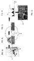
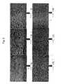
要約すると、本発明の方法は、例えばカーボンナノチューブなどのナノスケール繊維のような、基材に固定したナノスケール特徴部又はナノスケール対象物の制御されたパターンを形成するために液体の制御された分散及び蒸発を利用する。図1a及び1eの顕微鏡写真で示されるように、特に、図1aは幾何学的な再配向(reorientation)前のナノ繊維12の緻密な配列(array)を有する基材10を示し、そして図1eは幾何学的再配向後の同じナノ繊維を示す。図1bから1dは、本発明の制御されたパターン化方法の一実施態様を図解的に示す。図1bで示されるように、第一の工程で、複数の固定されたナノスケール特徴部12を有する基材10は液体材料14の液滴又は膜によって湿らされる。本プロセスの第二の工程で、図1bの矢印16で示されるように、液膜が複数の固定されたナノスケール特徴部12を覆って及び通じて(over and through)分散し(例えば図1cを参照)、図1dで示されるように、液膜14が消散し続けるにつれ、固定されたナノスケール特徴部はこの液膜によって及ぼされる毛管力によって集合的なナノ構造体18へ引き集められる。後に液膜が基材の表面から十分に消散したときに基材の表面に形成された個々のナノスケール特徴部12からなる大きな集合的構造体18の顕微鏡写真が図1eに示される。実際のサンプルでのこの形成プロセスの進行を示す顕微鏡写真が図2aから2fで提供される。(直接的な比較を提供するために図1及び2の集合群では同じ参照数詞が使用されることに留意のこと) In summary, the method of the present invention provides a controlled pattern of liquid to form a controlled pattern of nanoscale features or nanoscale objects affixed to a substrate, such as nanoscale fibers such as carbon nanotubes. Utilize dispersion and evaporation. In particular, as shown in the photomicrographs of FIGS. 1a and 1e, FIG. 1a shows a
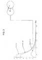
上記で論じたように、本発明の方法は個々のナノ特徴部を大きな集合的ナノ構造体へ制御可能に配列(arrange)しそしてパターン化するために流体の力を利用する。本プロセスの背後にある原理はこのナノ特徴部及び液体間の相互作用の性質に存する。例えば、対象物が液体の界面(interface)を貫くとき、これらの対象物は次式による力と関係する表面張力にさらされる。 As discussed above, the method of the present invention utilizes fluid forces to controllably arrange and pattern individual nanofeatures into large collective nanostructures. The principle behind the process resides in the nature of the interaction between this nanofeature and the liquid. For example, when objects penetrate the liquid interface, they are exposed to a surface tension that is related to a force according to:

ここでγが力であり、そしてαとθがこの対象物と液体の間の接触域を表す。これらの粒子間の距離に基づく粒子に対する力が図3にプロットされ、図3のサブセットにα及びθの図解的なダイアグラムが提供される。図3で示される力のプロットは、Ursoら、「索状液体ブリッジの破壊に関する二次元的研究」、(ケミカルエンジニアリングサイエンス57(4):677〜692、2002年2月)から引用し、この開示は参照としてここに組み込まれる。要するに、界面を貫くが、固体表面に支持されている小さい粒子、例えば本発明の固定されたナノ特徴部、に関して、この相互作用エネルギーはkT、熱エネルギーの何倍も大きい。さらに、同質の粒子に関してこの相互作用は常に引き合うことがよく知られている。例えば、〜10nm半径の水に浸した球状粒子に関して、エッジ間の分離距離が半径の2倍であるとき、引きあうエネルギーは〜100kTである。横引力を受ける2つのガラス管SEM(走査型電子顕微鏡)イメージが図4aに提供され、横力の方向を表すための矢印がそこに描かれている。この図4aで示されるSEM写真はVelveら、「横力の直接測定」(ラングミュア、9(12):3702〜3709、1993年12月)、から引用し、この開示は参照としてここに組み込まれる。この横引力の働きの図解が図4bで提供される。 Where γ is the force, and α and θ represent the contact area between the object and the liquid. The forces on the particles based on the distance between these particles are plotted in FIG. 3, and a schematic diagram of α and θ is provided in the subset of FIG. The force plot shown in FIG. 3 is taken from Urso et al., “Two-dimensional study on the destruction of cord-like liquid bridges”, (Chemical Engineering Science 57 (4): 677-692, February 2002). The disclosure is incorporated herein by reference. In short, for small particles that penetrate the interface but are supported on a solid surface, such as the immobilized nanofeatures of the present invention, this interaction energy is kT, many times greater than thermal energy. Furthermore, it is well known that this interaction is always attractive for homogeneous particles. For example, for a spherical particle immersed in water with a radius of 10 nm, when the separation distance between the edges is twice the radius, the energy to be attracted is ˜100 kT. Two glass tube SEM (scanning electron microscope) images subjected to lateral attraction are provided in FIG. 4a, where arrows are drawn to indicate the direction of the lateral force. The SEM photograph shown in FIG. 4a is taken from Velve et al., “Direct Measurement of Lateral Force” (Langmuir, 9 (12): 3702-3709, December 1993), the disclosure of which is incorporated herein by reference. . An illustration of this lateral attractive force action is provided in FIG. 4b.
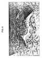
従って、複数のナノ特徴部が(そこに)配列(arrange)された基材が液体で処理されるとき、液−空気界面が生じ、この結果物は液−空気界面を貫く多数のナノ特徴部である(例えば図5aを参照)。結果として、大きな横毛管力が繊維に働く。脱濡れ又は蒸発の間に液体が後退するにつれて、これらの引力が個々のナノ特徴部が大規模なナノ構造体へ集合させていくことを次々に引き起こす(例えば図5b〜5dを参照)。リソグラフィーと関連するエッチアウト又はリフトオフプロセスとは反対に、本ナノパターン化技術は材料を切り出す又は加えることはしない、しかし表面にピン止めされた繊維を容易に撫でつける(comb)ために(ちょうど頭上の髪のように)これらの流体の力を利用する。ナノカーペット繊維は通常基板に向かって成長しそしてその土台に容易に固定されるので、キャピログラフィックパターンは自然な(概してナノチューブの長さによって与えられる高さの)シワ(corrugation)を有し、自由に浮遊する繊維(及び球体)の溶液を乾燥させた結果生じる表面フラッシュ(液体を勢いよく流す)パターンとは異なる。図6のSEM顕微鏡写真が本技術により形成されたナノ構造体の超拡大図を提供し、そしてナノ繊維の「撫でつけ」又は幾何学的再配向、及びこの幾何学的再配向の結果生じる表面のシワの両方を表している。 Thus, when a substrate having a plurality of nanofeatures arranged therein is treated with a liquid, a liquid-air interface is created, which results in a number of nanofeatures penetrating the liquid-air interface. (See, eg, FIG. 5a). As a result, a large transverse capillary force acts on the fiber. As the liquid recedes during dewetting or evaporation, these attractive forces in turn cause individual nanofeatures to assemble into large nanostructures (see, eg, FIGS. 5b-5d). Contrary to the etch-out or lift-off processes associated with lithography, the present nanopatterning technology does not cut or add material, but just to comb the fibers pinned on the surface (just overhead) Utilize the power of these fluids (like hair). Since nanocarpet fibers usually grow towards the substrate and are easily anchored to its foundation, the caprographic pattern has natural (generally the height given by the length of the nanotube) wrinkles (corrugation); This is different from the surface flush pattern that results from drying a solution of free-floating fibers (and spheres). The SEM micrograph of FIG. 6 provides a hyper-enlarged view of a nanostructure formed by the present technique, and the “striking” or geometrical reorientation of the nanofibers and the surface resulting from this geometrical reorientation Represents both wrinkles.
本技術は、大部分について恒久的にそれら(幾何学的再配向したナノ特徴部)を表面から除去することもなく、ナノ特徴部を容易に幾何学的再配向するために流体を利用するが、幾何学的再配向した後のナノ特徴部を支持する強いファンデルワールス力のために、このナノ構造体は頑丈であり、そして特に、付加的な湿潤及び乾燥プロセスによって影響を受けないことも理解される。従って、いったん本発明の幾何学的配向方法が完了すると、これらのナノ構造体が固定される。 Although this technique utilizes fluids to easily geometrically reorient nanofeatures without permanently removing them (geometrically reorientated nanofeatures) from the surface for the most part. Because of the strong van der Waals forces that support the nanofeatures after geometric reorientation, the nanostructure is robust and not particularly affected by additional wetting and drying processes. Understood. Thus, once the geometric orientation method of the present invention is complete, these nanostructures are fixed.
上記に記載された理論によっては結びつけられないが、ナノ特徴部の湿潤及び乾燥によって招かれた幾何学的再配向プロセスの間、ナノ特徴部のいくつかは径方向又は線形方向のいずれかに引張られる。加えて、いくつかの場合では流体の力がいくつかのナノ特徴部を基材から押しのけることさえあり得、基材に占有されない空隙を残したままにする。これらの集合的な線形又は径の幾何学的再配向の結果は溝状の又は反円状の構成(formation)を形成することである。基材、ナノ特徴部の特性、液体材料の特性、及び乾燥プロセスを制御することによって;個々のナノ特性のキャピログラフィック配列(arrangement)の結果生じる集合的なナノ構造体の寸法、形状及び幾何学的配向が制御可能である。本発明による種々の制御方法のまとめ、及びこれらの方法の結果として形成されるパターンが以下の表1に提供される。 While not being bound by the theory described above, during the geometric reorientation process caused by wetting and drying of the nanofeatures, some of the nanofeatures are either pulled in either the radial or linear direction. It is done. In addition, in some cases, fluid forces can even push some nanofeatures away from the substrate, leaving unoccupied voids in the substrate. The result of these collective linear or radial geometrical reorientations is to form a grooved or anti-circular formation. By controlling the substrate, nanofeature properties, liquid material properties, and drying process; the size, shape and geometry of the collective nanostructure resulting from the caprographic arrangement of individual nanofeatures The geometrical orientation can be controlled. A summary of the various control methods according to the present invention and the patterns formed as a result of these methods are provided in Table 1 below.
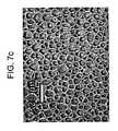
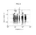
例えば、図7a〜7dは本発明の制御されたナノ構造体の特別な実施態様を種々の電子顕微鏡解像度で示し、ここでナノ構造体は半円形状をとっており、ここで「巣」ナノ構造体として言及される。図7a〜7dで示されるように、〜5μmの直径を有する「巣」ナノ構造体が本発明の制御されたキャピログラフィック方法によって形成された。しかしながら、上記で論じたように湿潤又は乾燥条件を修正することによって、このナノ特徴部の寸法及び性質、基材の幾何学的配向及び材料、これらの巣特徴部の寸法が制御可能である。図8はカーボンナノチューブで覆われた基材について多様な種々の条件を使用した一連の試験の結果を報告する。示されているように、キャピログラフィープロセスが実施される条件を変化させることによってナノ構造体の寸法が10μm未満から100μm超まで制御可能である。本プロセスからのデータに加えて、図8はまた別の群からのデータをプロットし、それらの方法により形成された特徴部がこのプロットに沿って減少(fall)するところを示す。この先行技術データは矢印及び文字(「a」はS.Liら、J.Phys.Chem. B106 9274〜9276(2002年)から;「b」はM.A. Correa−Duarteら、Nano Lettesr 4(11)2233〜2236(2004年)から;「c」はH.Liuら、Angew.Chemi.Int.Ed.43 1146〜1149(2004年)から;及び「d」はN.Chakrapaniら、PNAS101 409〜4012 (2004年)から引用)によって示される。示されるように、先行技術の方法は単一のナノ構造体の寸法を提供するだけであり、先行技術群はナノ構造体の寸法を制御可能に変化させるためプロセスを表していない。加えて、全ての先行技術結果はかなり狭い寸法分布範囲、約10μm〜約90μmに含まれる。 For example, FIGS. 7a-7d show particular embodiments of the controlled nanostructure of the present invention at various electron microscope resolutions, where the nanostructure has a semicircular shape, where “nest” nanostructures Referred to as a structure. As shown in FIGS. 7a-7d, “nest” nanostructures having a diameter of ˜5 μm were formed by the controlled capillographic method of the present invention. However, by modifying the wet or dry conditions as discussed above, the size and nature of the nanofeatures, the geometric orientation and material of the substrate, and the dimensions of these nest features can be controlled. FIG. 8 reports the results of a series of tests using a variety of different conditions on a substrate covered with carbon nanotubes. As shown, the size of the nanostructure can be controlled from less than 10 μm to more than 100 μm by changing the conditions under which the capillography process is performed. In addition to the data from this process, FIG. 8 also plots data from another group, showing the features formed by those methods fall along this plot. This prior art data includes arrows and letters ("a" from S. Li et al., J. Phys. Chem. B106 9274-9276 (2002); "b" from MA Correa-Duarte et al., Nano Letters 4 (11) From 2233 to 2236 (2004); “c” from H. Liu et al., Angew. Chemi. Int. Ed. 43 1146-11149 (2004); and “d” from N. Chakrapani et al., PNAS 101 409-4012 (2004)). As shown, the prior art methods only provide single nanostructure dimensions, and the prior art group does not represent a process for controllably changing nanostructure dimensions. In addition, all prior art results fall within a fairly narrow size distribution range, about 10 μm to about 90 μm.
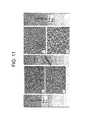
例えば、高いレベルの湿潤度を保つことがナノ特徴部の緩やかでかつ完全な再配列(rearrangement)及びパターン化を可能にし、結果としてよりおおきな巣構造を徐々にもたらし、一方で乾燥プロセスの速度を上げると巣の完全な形成を防ぐことが、見出された。加えて、「巣」の「完成」が乾燥条件によって決まるので、これらの半円状のナノ構造体の形状及び性質もまた乾燥及び湿潤条件を修正することにより制御されることが可能である。図9及び10は種々の乾燥条件下で形成された半円状のナノ構造体を示す。図9a及び9bにおいて、この乾燥は明確で完全な半円状構成(formation)がもたらされるように高い湿潤条件下でゆっくりと乾燥が行われた。対照的に、図10a及び10bでは乾燥プロセスが加速され、10aでは、表面に向けたファン(送風機)からのような、空気流れを使用し、そして10bでは、かなり高い揮発性を有する溶媒を使用する。図10a及び10bで示されるように、形成されたナノ構造体は大きな溝及び開いた辺を伴う巣を有し、巣の不完全な形成及び液体の非常に早い乾燥を示している。同様に、図11は湿潤度が増加する条件下でのナノ構造体の形成を撮影した一連の顕微鏡写真を示す。示されるように、湿潤度が増加するにつれてナノ構造体の数と密度の両方が上昇する。 For example, maintaining a high level of wetness allows gradual and complete rearrangement and patterning of the nanofeatures, resulting in a gradual result in a larger nest structure, while speeding up the drying process. It has been found that raising it prevents complete nest formation. In addition, since the “completion” of the “nest” depends on the drying conditions, the shape and properties of these semicircular nanostructures can also be controlled by modifying the drying and wetting conditions. Figures 9 and 10 show semicircular nanostructures formed under various drying conditions. In FIGS. 9a and 9b, this drying was performed slowly under high wet conditions to provide a clear and complete semicircular formation. In contrast, in FIGS. 10a and 10b, the drying process is accelerated, 10a uses an air stream, such as from a fan towards the surface, and 10b uses a solvent with a much higher volatility. To do. As shown in FIGS. 10a and 10b, the formed nanostructure has a nest with large grooves and open edges, indicating incomplete nest formation and very rapid drying of the liquid. Similarly, FIG. 11 shows a series of photomicrographs taken of nanostructure formation under conditions of increasing wetness. As shown, both the number and density of nanostructures increase as wetness increases.
しかし、単に基材の表面上のナノ構造体の配列(arrangement)及び密度を変化するだけでなく、乾燥条件はまたナノ構造体の構造を変化させる。例えば、図12a〜12cは種々の乾燥条件下での基材の上の「巣」形成の一連の顕微鏡写真を示し、図12aが最速の乾燥試料であり、図12cが最もゆっくり乾燥したものである。図12cが示すように、より慎重な乾燥プロセスは輪郭のはっきりした明確な壁を有する巣構成(formation)の創製を可能にし、一方でより早い条件ではナノチューブが輪郭のはっきりした小胞間の交差部を形成するための十分な時間が与えられない。従って、脱濡れプロセスの乾燥条件を変化させることによって、本方法により形成されたナノ構造体の数、密度、包み方(packing)及び形状が制御されることが可能である。 However, not only does the arrangement and density of the nanostructures on the surface of the substrate change, but the drying conditions also change the structure of the nanostructures. For example, FIGS. 12a-12c show a series of photomicrographs of “nest” formation on a substrate under various drying conditions, with FIG. 12a being the fastest dry sample and FIG. 12c being the slowest dry. is there. As FIG. 12c shows, a more careful drying process allows the creation of a nest formation with well-defined and well-defined walls, while in earlier conditions the nanotubes intersect between well-defined vesicles. Sufficient time is not given to form the part. Therefore, by changing the drying conditions of the dewetting process, the number, density, packing and shape of the nanostructures formed by the present method can be controlled.
さらに、巣及び溝の寸法がナノ特徴部の長さ及び構成(construction)によって決まるので、パターン又は寸法を変化させる他の方法はより大きな又はより小さなナノ特徴部を進歩的に提供することであろう。例えば、図6の顕微鏡写真で示されるように、ナノ構造体は基材の表面に向けて下向きにナノ特徴部を放射状(radial)に曲げることによって形成されるので、ナノ特徴部の長さと最終的なナノ構造体の面積との間に直接的な関係が存在する。従って、本発明の一実施態様において、本発明の方法によって形成されたナノ構造体の寸法は基材に配置(dispose)されたナノ特徴部の長さ及び直径によって制御される。このような実施態様において、寸法が可変である一連のナノ構造体を形成するために基材の種々の領域が種々の比率のナノ特徴部によって覆われてもよい。さらに、5μmほどの小ささでしかないナノ構造体が上記で論じられたが、一重壁の(single-walled)、サブミクロンナノチューブを使用することによってサブミクロン寸法のナノ構造体が形成されてもよい。 In addition, since the nest and groove dimensions are determined by the length and construction of the nanofeatures, other ways of changing the pattern or dimensions are to progressively provide larger or smaller nanofeatures. Let's go. For example, as shown in the micrograph of FIG. 6, the nanostructures are formed by bending the nanofeatures radially downward toward the surface of the substrate, so that the length and final length of the nanofeatures There is a direct relationship between the area of the typical nanostructure. Thus, in one embodiment of the present invention, the dimensions of the nanostructures formed by the method of the present invention are controlled by the length and diameter of the nanofeatures disposed on the substrate. In such embodiments, various regions of the substrate may be covered by various proportions of nanofeatures to form a series of nanostructures that are variable in size. In addition, nanostructures as small as 5 μm have been discussed above, but single-walled submicron nanotubes can be used to form submicron-sized nanostructures. Good.
最終的に、乾燥速度及び湿潤プロセスの性質は本質的にナノ特徴部にさらすために使用する液体によって決まるので、液体の性質を変化させることはナノ構造体の構成(formation)を制御するために使用されることも可能である。例えば、水よりも低い表面張力を有する界面活性剤溶液を使用することはカーボンナノチューブに関して見られるような疎水性表面へのより簡易な湿潤プロセスを可能にする。結果として、液体はナノチューブの内部に浸透することが可能であり、そして見かけ上(outward)長い距離にわたる芯(wick)となり得る。さらに、溶媒の粘度及び蒸気圧はまた、この液体がナノ特徴部を通じてどのように吸い上げられるか(wick)、毛管力がナノ特徴部に対してどれくらい強いか、そして液体がどれくらい早く乾燥するかも決定する。これらのパラメーターのいずれか一つを変化させることは形成されたナノ構造体の性質に重大な影響を持ち得る。例えば、図13はアセトンが湿潤液として使用される例を示す。このような低粘度、高蒸気圧の液体(例えばアセトン)を使用することはこれらの線形な構成(formation)の形成を加速させる。加えて、表1で述べたように、伝統的でない湿潤液、例えば表面にナノ構造体を完全に形成することに対する障壁が存在しないように長い時間表面に留まることが可能な非蒸発性液体又は液体材料中の固体の懸濁からなる液体、が使用されてもよい。このような風変わりな材料は、図14aで見られる「割れた」表面パターンのような、独特の表面構造を創製することが可能である。この例では水中のポリスチレン高分子微粒子の懸濁液が表面に適用された。図14bの高解像度イメージで見られるように、高分子微粒子が、ナノ特徴部表面に割れ(crack)状の溝を形成するように線状に一緒になって集まる。従って、表1で論じたように、ナノ特徴部がさらされる液体を変化させることもまた本発明のナノ構造体の性質を制御するために使用されてもよい。 Finally, since the drying rate and the nature of the wetting process are essentially determined by the liquid used to expose the nanofeatures, changing the properties of the liquid is necessary to control the nanostructure formation. It can also be used. For example, using a surfactant solution that has a lower surface tension than water allows a simpler wetting process to the hydrophobic surface as seen with carbon nanotubes. As a result, the liquid can penetrate into the interior of the nanotube and can appear to be a wick over long distances. In addition, the viscosity and vapor pressure of the solvent also determine how this liquid is wicked through the nanofeature, how strong the capillary force is against the nanofeature, and how quickly the liquid dries. To do. Changing any one of these parameters can have a significant impact on the properties of the nanostructure formed. For example, FIG. 13 shows an example where acetone is used as the wetting liquid. Using such a low viscosity, high vapor pressure liquid (eg, acetone) accelerates the formation of these linear formations. In addition, as described in Table 1, non-traditional wetting liquids, such as non-evaporable liquids that can remain on the surface for long periods of time so that there is no barrier to the complete formation of nanostructures on the surface or A liquid consisting of a suspension of a solid in a liquid material may be used. Such quirky materials can create unique surface structures, such as the “cracked” surface pattern seen in FIG. 14a. In this example, a suspension of polystyrene polymer particles in water was applied to the surface. As can be seen in the high resolution image of FIG. 14b, the polymer microparticles gather together in a line to form cracked grooves on the nanofeature surface. Thus, as discussed in Table 1, changing the liquid to which the nanofeature is exposed may also be used to control the properties of the nanostructures of the present invention.
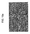
表1で論じたように、基材もまた本発明により形成されたナノ構造体を制御するために使用されることが可能である。例えば、基材は、ナノ特徴部の成長のために求められる温度に耐えることができ、そして好適なナノメカニカルデバイスを集積するための基材の特定の領域にナノ構造体を制御可能に配置(position)するための核生成領域を提供するために随意的に修正されることが可能な、任意の材料から製造されてもよい。好適な基材の例は金属化した(metallized)Si酸化物ウェハー、アルミナ、又はサファイアを含む。さらに、本出願の実施例では堅い(rigid)基材のみが考慮されるが、表1で論じたように、本発明のキャピログラフィック技術は、柔軟性のある又は湾曲した表面のような、任意の曲率の表面に適用することができる。例えば、一実施態様では、ナノ特徴部は最初は、Siのように、堅い基材の上で成長させられ、そしてその後柔軟性テープのような付着物がナノチューブの頂部に適用される。このテープの付着力は、一度適用すると、ナノチューブがテープと共に除去される程度のものである。このやり方でナノチューブは堅い基材から柔軟な基材へ移動させられ、そしてその後通常通りに扱われることが可能である。加えて、基材の成長前(pre-growth)の条件もまたそこで成長するナノ特徴部の制御されたパターン化を導くことが可能である。例えば、図15a及び15bはナノ特徴部の成長の前に基材の表面にマクロ規模の擦り傷が作られた実施態様を示す。示されるように、幾何学的再配向の間、ナノチューブは特徴部から離れて曲げられて秩序だった「巣」構成(formation)によって囲まれた深い溝を形成する。 As discussed in Table 1, substrates can also be used to control nanostructures formed according to the present invention. For example, the substrate can withstand the temperatures required for the growth of nanofeatures and the controllable placement of nanostructures in specific areas of the substrate for the integration of suitable nanomechanical devices ( It may be made from any material that can be optionally modified to provide a nucleation region for position). Examples of suitable substrates include metallized Si oxide wafers, alumina, or sapphire. Furthermore, although only rigid substrates are considered in the examples of the present application, as discussed in Table 1, the capillographic technique of the present invention is such as flexible or curved surfaces, It can be applied to any curvature surface. For example, in one embodiment, the nanofeature is initially grown on a rigid substrate, such as Si, and then a deposit such as a flexible tape is applied to the top of the nanotube. The adhesive force of this tape is such that once applied, the nanotubes are removed along with the tape. In this manner, the nanotubes can be transferred from a rigid substrate to a flexible substrate and then handled as usual. In addition, pre-growth conditions of the substrate can also lead to controlled patterning of the nanofeatures growing there. For example, FIGS. 15a and 15b show an embodiment in which macroscale scratches have been created on the surface of the substrate prior to nanofeature growth. As shown, during geometric reorientation, the nanotubes are bent away from the feature to form deep grooves surrounded by an ordered “nest” formation.
加えて、基材の実際の材料及び条件を修正することに対して、基材の幾何学的配向、及び順にそこのナノ特徴部もまたナノ構造体を修正するために使用されることが可能である。本発明のキャピログラフィー方法によって形成されるナノ構造体はナノ特徴部を新しい位置(alignment)へと引いたり押したりする流体の力によって創製されるので、重力がナノ構造体の形態についてある役割を果たす。従って、基材を垂直又は角度のついた位置に幾何学的再配向することはナノ構造体の幾何学的配向及び構造を変化させることが可能である。例えば、図16は基材が垂直な幾何学的配向に支持された試験の結果を示す。示されるように、このキャピログラフィープロセスによって形成された「巣」はナノ特徴部に対して垂直に作用する重力の結果として変形される。 In addition, while modifying the actual material and conditions of the substrate, the geometric orientation of the substrate, and in turn the nanofeatures there, can also be used to modify the nanostructure It is. Since nanostructures formed by the capillography method of the present invention are created by the force of fluid that pulls and pushes nanofeatures to new alignments, gravity plays a role in the morphology of nanostructures Fulfill. Thus, geometrical reorientation of the substrate to a vertical or angled position can change the geometric orientation and structure of the nanostructure. For example, FIG. 16 shows the results of a test where the substrate was supported in a vertical geometric orientation. As shown, the “nest” formed by this capillography process is deformed as a result of gravity acting perpendicular to the nanofeatures.
状況によっては、例えばニッケル又はコバルトのような、任意の好適な触媒金属が基材の表面の核生成領域のために使用されることが可能である。あるいは、触媒金属はCo/Ni又はTi/Ni合金のような二以上の金属の合金でもよい。金属触媒は、例えば硝酸鉄又は塩化コバルトのような、無機又は有機金属含有化合物の熱分解によって創製されることも可能である。本発明に関してこのような触媒領域を50nm以下(sub-50nm)の触媒点の制限に制御することは必須ではないが可能であり、それゆえより大きなナノ検知器の範囲内でナノ構造体の適当な配置(placement)を確実にするための適切な制御以上のものを提供するために触媒の位置で単一のナノチューブの成長の核となることが可能である。活性化を求められるナノスケールデバイスに関して、集積した電子は非触媒の又は触媒の電極を伴う触媒領域を結合することによって創製されることも可能である。ナノ構造体の成長を正確に決めそして配向(locate and orient)しかつナノ特徴部への電気的接点を作る能力は作動構造体の製造のための基礎を提供する。 In some situations, any suitable catalytic metal, such as nickel or cobalt, can be used for the nucleation region on the surface of the substrate. Alternatively, the catalytic metal may be an alloy of two or more metals such as Co / Ni or Ti / Ni alloys. Metal catalysts can also be created by thermal decomposition of inorganic or organic metal-containing compounds such as iron nitrate or cobalt chloride. In the context of the present invention, it is possible, but not essential, to control such a catalytic region to a catalytic point limit of 50 nm or less (sub-50 nm), and therefore suitable for nanostructures within a larger nanodetector. It is possible to become the core of single nanotube growth at the location of the catalyst to provide more than adequate control to ensure proper placement. For nanoscale devices that require activation, integrated electrons can also be created by combining catalytic regions with non-catalytic or catalytic electrodes. The ability to accurately determine and orient the growth of nanostructures and make electrical contacts to nanofeatures provides the basis for the fabrication of working structures.
上記で論じた実施態様にナノチューブのナノスケール構造体が示されるが、表面に固定することが可能な任意の好適なナノスケール構造体が使用されてもよいことが理解される。しかしながら、好ましい実施態様では、上記で論じたように、複数のカーボンナノチューブが利用される。カーボンナノチューブは本発明のキャピログラフィック技術で使用するためにそれら(カーボンナノチューブ)を非常に好適なものにならしめる特性の組合せを有する。例えば、ナノチューブはナノメートル規模の直径を大きなアスペクト比、良好な電気伝導性、及び弾力のある撓みと結びつける。ナノチューブの湾曲の小さい半径は、個々のナノチューブの「付着(sticking)」能力に寄与する大きなファンデルワールス力を示している。カーボンナノチューブはまた疎水性であり、ともに液体環境にあることを要求されるときに、ナノチューブの相互作用を促す。一重壁の(Single-walled)ナノチューブはまた約1TPaのヤング率を有し、これは鉄の200倍に近い強度/質量比に対応する。この高いヤング率及び大きな歪み(〜5%)に耐える能力の組合せはSWNT(Single-walled nanotube)がまた非常に高い破壊強度も有し、大きな再構築力を適用することを可能にする。 Although the nanoscale structures of nanotubes are shown in the embodiments discussed above, it is understood that any suitable nanoscale structure that can be immobilized on a surface may be used. However, in a preferred embodiment, as discussed above, multiple carbon nanotubes are utilized. Carbon nanotubes have a combination of properties that make them (carbon nanotubes) highly suitable for use in the capillographic technology of the present invention. For example, nanotubes combine nanometer-scale diameters with large aspect ratios, good electrical conductivity, and elastic deflection. The small radius of curvature of the nanotubes indicates a large van der Waals force that contributes to the “sticking” ability of individual nanotubes. Carbon nanotubes are also hydrophobic, facilitating nanotube interaction when both are required to be in a liquid environment. Single-walled nanotubes also have a Young's modulus of about 1 TPa, which corresponds to a strength / mass ratio close to 200 times that of iron. This combination of high Young's modulus and ability to withstand large strains (~ 5%) allows SWNTs (Single-walled nanotubes) to also have very high fracture strength, allowing large rebuilding forces to be applied.
例えば、化学気相付着(CVD)技術のような、任意の好適な方法が基材にナノ特徴部の緻密なマットを成長させるために使用されてもよい。図1aに示される緻密なナノ特徴部の基材のような、整列した構造体を構築するための基本技術は、Si又はSOIのような、好適な基材を使用する。適当な成長を確実なものにするため、ナノ特徴部が成長する領域はナノ特徴部の成長の核となるNi、Co、又は他の金属系の混合物又は化合物のような薄い触媒膜で覆われてもよい。支持体及び電極を形成するために利用される基材にかかわらず、化学気相付着プロセス(CVD)が触媒パターンからナノチューブを成長させるために利用される。一実施態様において、高圧力CVDプロセスが、約500〜1000℃に加熱した基材でナノチューブを創製するために、メタン、エチレン、又は一酸化炭素を純粋な形態又は水素(又はアンモニア)及びアルゴン(又は窒素)との混合で使用する。 Any suitable method may be used to grow a dense mat of nanofeatures on a substrate, such as, for example, chemical vapor deposition (CVD) techniques. The basic technique for constructing aligned structures, such as the dense nanofeature substrate shown in FIG. 1a, uses a suitable substrate, such as Si or SOI. To ensure proper growth, the area in which the nanofeatures grow is covered with a thin catalyst film such as Ni, Co, or other metal-based mixture or compound that is the core of the nanofeature growth. May be. Regardless of the substrate utilized to form the support and electrodes, a chemical vapor deposition process (CVD) is utilized to grow the nanotubes from the catalyst pattern. In one embodiment, a high pressure CVD process is used to create methane, ethylene, or carbon monoxide in pure form or hydrogen (or ammonia) and argon (to create nanotubes on a substrate heated to about 500-1000 ° C. Or mixed with nitrogen).
また、カーボンナノチューブの自己組み立てのための方法が上記で論じられたが、ナノ構造体を分析器とともに集積するときに必要になるようなCMOS電子技術でカーボンナノチューブ発信器を組み込むために、CMOS回路の処理と両立する温度、すなわち約500℃以下、でカーボンナノチューブの成長を提供することが必要なことが理解される。任意の好適な低温成長の方法が使用されるが、いくつかの方法の例として以下が含まれる:1)村上ら、(Appl. Phys. Lett. 76(13), 1776(2000)) パターン化されたニッケル系触媒上で1〜3Torrでバイアス強化マイクロ波プラズマCVDを使用して<600℃での電界放出のためのカーボンナノチューブ配列(array)を成長させる方法;2)Liら、(Appl. Phys. Lett. 79(11),1670(2001)) 100TorrでCVDを使用して570℃でガラス上で配列されていない(un align)ナノチューブを成長させる方法;3)シリコン上でのカーボンナノチューブを成長させるための低温プロセス(Choiら、J.Vac. Sci. Technol. A, 18(4), 1864(2000):付着強化層としてのTiN及び二酸化珪素で覆われたシリコン基材に配置(deposit)した触媒としての70nmニッケル膜を500〜550℃で使用する(Leeら、Chemi. Phys. Lett. 327, 277(2000));4)Zhangと飯島(Appl. Phys. Lett., 75(20), 3087(1999))Ni−Coを含む粉末触媒とともにレーザーアブレーション技術を使用して一重壁のカーボンナノチューブを約400℃で成長させる方法;5)Chenら(J. Cryst. Growth, 193, 342 (1998))グラファイトナノ繊維をニッケル基材上で350〜400℃で成長させる方法。これらの全てが参照としてここに組み込まれる。 A method for self-assembly of carbon nanotubes has also been discussed above, but in order to incorporate carbon nanotube transmitters in CMOS electronic technology as required when integrating nanostructures with analyzers, CMOS circuits It will be appreciated that it is necessary to provide carbon nanotube growth at a temperature compatible with this process, i.e., below about 500 ° C. Any suitable low temperature growth method can be used, but some examples include: 1) Murakami et al. (Appl. Phys. Lett. 76 (13), 1776 (2000)) Patterning Of growing carbon nanotube arrays for field emission at <600 ° C. using bias-enhanced microwave plasma CVD at 1-3 Torr over a modified nickel-based catalyst; 2) Li et al. (Appl. Phys. Lett. 79 (11), 1670 (2001)) A method of growing unaligned nanotubes on glass at 570 ° C. using CVD at 100 Torr; 3) Carbon nanotubes on silicon Low temperature process for growth (Choi et al., J. Vac. Sci. Technol. A, 18 (4), 1864 (2000): deposited on a silicon substrate covered with TiN and silicon dioxide as an adhesion strengthening layer 70 nm nickel film as a catalyst at 500 to 550 ° C. Used (Lee et al., Chemi. Phys. Lett. 327, 277 (2000)); 4) Zhang and Iijima (Appl. Phys. Lett., 75 (20), 3087 (1999)) Ni-Co containing powder catalyst And a method of growing single-walled carbon nanotubes at about 400 ° C. using laser ablation technology; 5) Chen et al. (J. Cryst. Growth, 193, 342 (1998)) 350 nm of graphite nanofibers on a nickel substrate. Method of growing at ~ 400 ° C. All of these are hereby incorporated by reference.
これまでに論じた実施態様において熟慮された自己組み立てナノ構造体がエチレン供給原料の基材上での熱分解から創られたカーボンナノチューブの緻密なマットから構築されてきた一方で、ナノ構造体を含むナノ特徴部は、例えば他の原子材料又はさらに例えばタンパク質のような生体分子から製造される球体又はピラミッド型のように、任意の形状であり、そして任意のプロセスによって製造され、そして自己組み立て構造体を創るために好適な任意の材料からなることが可能である。別の実施態様では、ナノ特徴部はさらに、例えば親水性又は疎水性にされること、マイナス又はプラスのいずれかに電荷されること、又は特定の化学基で誘導化されること等のような、多様な用途のために機能付加されてもよい。加えて、処理していないカーボンナノチューブのナノ構造体だけがここまで示されたが、例えば所与の印加電圧で変異誘導された電荷を増加することによって、そのままで側壁(sidewall)処理がナノチューブの電気的特性を変化させることが可能である。 While the self-assembled nanostructures contemplated in the embodiments discussed so far have been constructed from a dense mat of carbon nanotubes created from pyrolysis on an ethylene feedstock substrate, the nanostructures are The nanofeatures to include can be of any shape, such as spheres or pyramids manufactured from other atomic materials or even biomolecules such as proteins, and manufactured by any process, and self-assembled structures It can be made of any material suitable for creating a body. In another embodiment, the nanofeature is further made, for example, made hydrophilic or hydrophobic, charged negatively or positively, or derivatized with a specific chemical group, etc. Functionality may be added for various uses. In addition, only carbon nanotube nanostructures that have not been treated have been shown so far, but the sidewall treatment remains intact as it is, eg, by increasing the mutagenized charge at a given applied voltage. It is possible to change the electrical characteristics.
最終的に、上記の議論は基本的なナノ構造体の構築及び構造に焦点があたっていたが、本発明によるナノ構造体で製造された検知器のようなデバイスはまた本体(body)、内蔵型電源、及びこのデバイスの稼働に必要な任意の付加的機械又は回路も含んでもよい。例えば、ナノメカニカルデバイスの本体自身は、例えば酸化アルミニウム又はシリコンのような、ナノ構造体を閉じこめるために標準的なリソグラフィック又はMEMS技術を利用するマイクロマシニングのために好適な任意の材料から創られることが可能である。好ましい実施態様では、キャップ層が外部環境との望ましくない接触から制御されたナノ構造体を保護するように、本体はキャップ層をさらに含み、このキャップ層は任意の設計にすることが可能である。このようなキャップ層は、例えば酸化アルミニウム又はシリコンのような、任意の好適な材料から創られることが可能である。このようなキャップ層は、自己組み立てしたナノ構造体を密封するために付着した犠牲層(図示しない)での成長又は付着のような、任意の従来のMEMSプロセスによって形成されることが可能である。ここでこの犠牲層はナノ構造体自身を曝すために実質的に除去されることが可能である。あるいは、これらの支持構造体は自己組み立てナノ構造体とともに単一の付着工程で形成されることが可能である。より好ましい実施態様では、光源がナノ構造体を調査する(interrogate)又は活性化する(activate)ために使用されることが可能であるように、ナノメカニカルデバイスの基材、キャップ層、又は壁の一つは透明である。 Finally, while the above discussion focused on the construction and structure of basic nanostructures, devices such as detectors made with nanostructures according to the present invention are also A mold power supply and any additional machines or circuits necessary to operate the device may also be included. For example, the body of the nanomechanical device itself is created from any material suitable for micromachining using standard lithographic or MEMS techniques to confine the nanostructure, such as aluminum oxide or silicon, for example. It is possible. In a preferred embodiment, the body further includes a cap layer, and the cap layer can be of any design so that the cap layer protects the controlled nanostructure from unwanted contact with the external environment. . Such a cap layer can be made from any suitable material, such as, for example, aluminum oxide or silicon. Such a cap layer can be formed by any conventional MEMS process, such as growth or deposition on a sacrificial layer (not shown) deposited to seal the self-assembled nanostructure. . Here the sacrificial layer can be substantially removed to expose the nanostructure itself. Alternatively, these support structures can be formed with a self-assembly nanostructure in a single attachment step. In a more preferred embodiment, the light source can be used to interrogate or activate the nanostructure so that the substrate, cap layer, or wall of the nanomechanical device can be used. One is transparent.
他の代替的な実施態様では、本発明による制御されたナノ構造体を有するデバイスは、複数の又は平行プロセシングが一度に実施されることが出来るように、複数のナノ構造体の配列(array)を含んでもよい。この実施態様では、ナノ構造体は単一の回路又は検知機器に集積されることが可能である。ナノ構造体の配列(array)が上記で議論されるが、任意の好適な代替的なナノ構造体の配列(geometry)が利用されてもよい。このような実施態様は試料の携帯可能な検知及び分析のためのチップ上の携帯可能なナノ構造検知器デバイスを開発するために使用されることが可能である。このような実施態様では、持ち運びできる電源(図示しない)もまたデバイスに集積される。 In another alternative embodiment, a device having controlled nanostructures according to the present invention is an array of multiple nanostructures so that multiple or parallel processing can be performed at once. May be included. In this embodiment, the nanostructures can be integrated into a single circuit or sensing device. Although an array of nanostructures is discussed above, any suitable alternative nanostructure array may be utilized. Such an embodiment can be used to develop a portable nanostructure detector device on a chip for portable detection and analysis of samples. In such an embodiment, a portable power supply (not shown) is also integrated into the device.
さらに、上記の議論は本発明による実際の制御されたナノ構造体及びそれらの制御されたナノ構造体を形成する方法に向けられていたが、本発明はまた上記の図で図解的に示されたナノ構造体を含む好適なナノメカニカルデバイスにも向けられることが理解される。 Furthermore, while the above discussion has been directed to actual controlled nanostructures and methods of forming those controlled nanostructures according to the present invention, the present invention is also illustrated schematically in the above figures. It is understood that the present invention is also directed to suitable nanomechanical devices including nanostructures.
本発明の範囲はまた以下の、非限定的な例、を参照して理解される。この例は、本発明の方法により形成されたナノ構造体を変化させるために、ここで議論されたパラメーターのいくつかの働き(operation)がどのように使用されることが可能であるかを示すために提供される。 The scope of the invention is also understood with reference to the following, non-limiting examples. This example shows how several operations of the parameters discussed here can be used to change the nanostructures formed by the method of the present invention. Provided for.
例1
35μmの長さのナノチューブを、2nmのFeで金属化した石英(アモルファスSiO2、スライドガラス)基材上で約20〜30nmの直径から成長させた。それから表面を横切るファン(送風機)のブローを伴いつつ、(画像化のために)顕微鏡対象物の下に座した状態で、0.5CMC(臨界ミセル濃度、これはSDSに対して約8.2mMである)のSDSに10分間さらした。結果物であるパターンは、結合しない尾根の未完成のパターンと同様に、概して平均直径で100μmの巣(半円状)から構成(comprise)され、基材表面に達しない長い谷及び溝を効果的に形成した。この方法により形成されたナノ構造体のSEMは図10aで提供される。Example 1
35 μm long nanotubes were grown from a diameter of approximately 20-30 nm on a quartz (amorphous SiO2 , slide glass) substrate metallized with 2 nm Fe. Then, with the blow of a fan (blower) across the surface and sitting under the microscope object (for imaging), 0.5 CMC (critical micelle concentration, which is about 8.2 mM relative to SDS). For 10 minutes. The resulting pattern, similar to the unfinished pattern of unconnected ridges, is generally composed of 100 μm nests (semi-circular shape) with an average diameter, and effects long valleys and grooves that do not reach the substrate surface. Formed. An SEM of the nanostructure formed by this method is provided in FIG. 10a.
例2
25分間の晒し及び表面を横切るファンのブローは伴わなかったことを除いて、例1に記載された方法を使用した。この方法は結果として整然とした高度に多角形化した約60〜70μmの平均直径の巣をもたらした。本方法により形成したナノ構造体のSEMが図9aに提供される。Example 2
The method described in Example 1 was used, except that there was no 25 minutes exposure and no blow of fan across the surface. This method resulted in an orderly highly polygonal nest with an average diameter of about 60-70 μm. An SEM of the nanostructure formed by this method is provided in FIG. 9a.
例3
長さ4μm、かつ約35〜50nmの直径のナノチューブを2nmのNi及び2nmのTiで金属化(metallize)したSiO2上で成長させ、その後よい換気の条件下で一晩小さな体積部を純水と細菌胞子との溶液にさらした。形成したパターンは4μmの平均直径のほぼ円形の巣の高度に整然と分布したものであり、それら(巣)の間に比較的幅の広い障壁となる尾根を伴っていた(例えば、直径に対する幅の比が大きい)。本方法により形成したナノ構造体のSEMが図7a〜7dに提供される。Example 3
Nanotubes with a length of 4 μm and a diameter of about 35-50 nm were grown on SiO2 metallized with 2 nm Ni and 2 nm Ti, and then a small volume was purified with pure water overnight under good ventilation conditions. And exposed to a solution of bacterial spores. The pattern formed was a highly orderly distribution of nearly circular nests with an average diameter of 4 μm, with a ridge that was a relatively wide barrier between them (for example, Ratio is large). SEMs of the nanostructures formed by this method are provided in FIGS.
特定の実施態様及び例示的な実施態様がここで開示されたが、当業者は、文字通り又は均等論のいずれかにより以下の請求項の範囲内である、代替の制御されたナノ構造体及びナノ構造体の組合せ及びナノ構造体を製造する方法を設計することが可能でありそうするであろうことが予期される。 While specific embodiments and exemplary embodiments have been disclosed herein, those skilled in the art will recognize alternative controlled nanostructures and nanostructures that are either within the scope of the following claims, either literally or by an equivalent theory. It is anticipated that it will be possible and likely to design a combination of structures and methods of manufacturing nanostructures.
Claims (34)
Translated fromJapanese基材の少なくとも一端に固定された複数のナノ特徴部を提供すること;
該複数のナノ特徴部の少なくとも一部に、該複数のナノ特徴部の間に浸透するように十分低い表面張力を有する液体をある量で配置(dispose)すること;
液体の消散によってナノ特徴部が再配向され、再配向されたナノ特徴部から複数の反復的な(repeating)ナノ構造体を形成するように、特定の速度で該複数のナノ特徴部から液体を消散させることを含んでなる方法。A method for controllably patterning a plurality of nanofeatures, comprising the following steps:
Providing a plurality of nanofeatures secured to at least one end of the substrate;
Disposing at least a portion of the plurality of nanofeatures with an amount of a liquid having a sufficiently low surface tension to penetrate between the plurality of nanofeatures;
The liquid is dissipated from the plurality of nanofeatures at a specific rate so as to reorient the nanofeatures by liquid dissipation and form a plurality of repeating nanostructures from the reoriented nanofeatures. A method comprising dissipating.
柔軟な付着性材料をナノ特徴部の上面に適用すること;
プロセスの後工程に関しては接着材料が基材となるように、ナノ特徴部が基材から除去されるが接着材料には付着したままであるように、接着材料を剥がすこと、をさらに含んでなる請求項12に記載された方法。Prior to placing the liquid on the nanofeature, the following steps:
Applying a flexible adhesive material to the top surface of the nanofeature;
Further comprising peeling off the adhesive material so that the nanofeatures are removed from the substrate but remain attached to the adhesive material such that the adhesive material becomes the substrate with respect to subsequent steps of the process. The method according to claim 12.
Applications Claiming Priority (2)
| Application Number | Priority Date | Filing Date | Title |
|---|---|---|---|
| US56856304P | 2004-05-05 | 2004-05-05 | |
| PCT/US2005/015796WO2006041535A2 (en) | 2004-05-05 | 2005-05-05 | Capillary lithography of nanofiber arrays |
Publications (1)
| Publication Number | Publication Date |
|---|---|
| JP2007536101Atrue JP2007536101A (en) | 2007-12-13 |
Family
ID=36148756
Family Applications (1)
| Application Number | Title | Priority Date | Filing Date |
|---|---|---|---|
| JP2007511622APendingJP2007536101A (en) | 2004-05-05 | 2005-05-05 | Nanofiber array capillary lithography |
Country Status (4)
| Country | Link |
|---|---|
| US (1) | US7491628B2 (en) |
| EP (1) | EP1747576A2 (en) |
| JP (1) | JP2007536101A (en) |
| WO (1) | WO2006041535A2 (en) |
Cited By (5)
| Publication number | Priority date | Publication date | Assignee | Title |
|---|---|---|---|---|
| WO2010074365A1 (en)* | 2008-12-22 | 2010-07-01 | 한국과학기술원 | Method for arranging nanomaterials using solution evaporation |
| WO2010056933A3 (en)* | 2008-11-14 | 2010-07-29 | The University Of Akron | Hydrophobic surface coating systems and methods for metals |
| US7927666B2 (en) | 2006-06-30 | 2011-04-19 | The University Of Akron | Aligned carbon nanotube-polymer materials, systems and methods |
| US9095639B2 (en) | 2006-06-30 | 2015-08-04 | The University Of Akron | Aligned carbon nanotube-polymer materials, systems and methods |
| JP2016003180A (en)* | 2014-06-18 | 2016-01-12 | ツィンファ ユニバーシティ | Process for producing patterned carbon nanotube array and carbon nanotube element |
Families Citing this family (24)
| Publication number | Priority date | Publication date | Assignee | Title |
|---|---|---|---|---|
| DE10312628A1 (en)* | 2003-03-21 | 2004-10-07 | Friz Biochem Gmbh | Method and device for wetting a substrate with a liquid |
| CN100463111C (en)* | 2006-01-14 | 2009-02-18 | 清华大学 | Preparation method of silicon wire |
| US8846143B2 (en) | 2006-07-10 | 2014-09-30 | California Institute Of Technology | Method for selectively anchoring and exposing large numbers of nanoscale structures |
| EP2081869B1 (en) | 2006-07-10 | 2020-11-04 | California Institute of Technology | Method for selectively anchoring large numbers of nanoscale structures |
| US7959969B2 (en) | 2007-07-10 | 2011-06-14 | California Institute Of Technology | Fabrication of anchored carbon nanotube array devices for integrated light collection and energy conversion |
| US8647922B2 (en)* | 2007-11-08 | 2014-02-11 | Nanyang Technological University | Method of forming an interconnect on a semiconductor substrate |
| US8906335B2 (en)* | 2008-05-29 | 2014-12-09 | Lockheed Martin Corporation | System and method for broad-area synthesis of aligned and densely-packed carbon nanotubes |
| WO2013154750A1 (en) | 2012-04-10 | 2013-10-17 | The Trustees Of Columbia Unversity In The City Of New York | Systems and methods for biological ion channel interfaces |
| US8192685B2 (en) | 2008-11-04 | 2012-06-05 | Advanced Concepts And Technologies International, L.L.C. | Molecular separators, concentrators, and detectors preparatory to sensor operation, and methods of minimizing false positives in sensor operations |
| EP2381972A2 (en) | 2009-01-27 | 2011-11-02 | California Institute Of Technology | Drug delivery and substance transfer facilitated by nano-enhanced device having aligned carbon nanotubes protruding from device surface |
| WO2010120564A2 (en)* | 2009-03-31 | 2010-10-21 | The Regents Of The University Of Michigan | Shaping nanostructure arrays |
| US9115424B2 (en) | 2010-04-07 | 2015-08-25 | California Institute Of Technology | Simple method for producing superhydrophobic carbon nanotube array |
| WO2012031164A2 (en) | 2010-09-02 | 2012-03-08 | California Institute Of Technology | Drug delivery by carbon nanotube arrays |
| WO2012079066A2 (en) | 2010-12-10 | 2012-06-14 | California Institute Of Technology | Method for producing graphene oxide with tunable gap |
| CN103620403B (en) | 2011-01-11 | 2016-08-10 | 纽约市哥伦比亚大学理事会 | Systems and methods for monitoring single molecules using nanotubes |
| CN103380369B (en) | 2011-02-23 | 2016-12-28 | 纽约市哥伦比亚大学理事会 | Nano-pore is used to carry out the system and method for Single Molecule Detection |
| US8976507B2 (en) | 2011-03-29 | 2015-03-10 | California Institute Of Technology | Method to increase the capacitance of electrochemical carbon nanotube capacitors by conformal deposition of nanoparticles |
| CN103889595B (en)* | 2011-07-01 | 2016-06-22 | 凯博瑞奥斯技术公司 | Anisotropic reduction in the coating of conducting film |
| WO2013090844A1 (en) | 2011-12-14 | 2013-06-20 | California Institute Of Technology | Sharp tip carbon nanotube microneedle devices and their fabrication |
| WO2013158280A1 (en) | 2012-04-20 | 2013-10-24 | The Trustees Of Columbia University In The City Of New York | Systems and methods for single-molecule nucleic-acid assay platforms |
| US9349543B2 (en) | 2012-07-30 | 2016-05-24 | California Institute Of Technology | Nano tri-carbon composite systems and manufacture |
| US10006085B2 (en) | 2013-11-04 | 2018-06-26 | The Regents Of The University Of California | Nanostructured arrays on flexible polymer films |
| CN109231151A (en)* | 2018-09-26 | 2019-01-18 | 天津大学 | A kind of device and application for making self-assembly structure |
| CN110767515B (en)* | 2019-10-21 | 2020-10-27 | 北京师范大学 | A preparation method of carbon nanotube array beam with adjustable aspect ratio applied to field emission cold cathode |
Family Cites Families (89)
| Publication number | Priority date | Publication date | Assignee | Title |
|---|---|---|---|---|
| US552981A (en)* | 1896-01-14 | William bolinger | ||
| JPS525857B2 (en)* | 1972-10-23 | 1977-02-17 | ||
| US4008136A (en)* | 1974-08-09 | 1977-02-15 | Temple University | Process for the treatment of waste water by heterogeneous photosensitized oxidation |
| JPS5315152A (en)* | 1976-07-27 | 1978-02-10 | Canon Inc | Hologram |
| US4173475A (en)* | 1977-05-31 | 1979-11-06 | Bell Telephone Laboratories, Incorporated | Latent image thick refractive index recordings |
| US4330383A (en)* | 1978-07-18 | 1982-05-18 | Polymer Technology Corporation | Dimensionally stable oxygen permeable hard contact lens material and method of manufacture |
| US4260725A (en)* | 1979-12-10 | 1981-04-07 | Bausch & Lomb Incorporated | Hydrophilic contact lens made from polysiloxanes which are thermally bonded to polymerizable groups and which contain hydrophilic sidechains |
| JPS60175009A (en) | 1984-02-21 | 1985-09-09 | Nippon Sheet Glass Co Ltd | Production of plastic optical element having refractive index distribution |
| US4575373A (en)* | 1984-11-02 | 1986-03-11 | Johnson Don R | Laser adjustable intraocular lens and method of altering lens power |
| JPS61190546A (en) | 1985-02-20 | 1986-08-25 | Central Glass Co Ltd | Resin composition for optical use |
| US4787903A (en)* | 1985-07-24 | 1988-11-29 | Grendahl Dennis T | Intraocular lens |
| US4685921A (en)* | 1986-02-24 | 1987-08-11 | Peyman Gholam A | Variable refractive power, expandable intraocular lenses |
| US4790847A (en)* | 1987-05-26 | 1988-12-13 | Woods Randall L | Intraocular lens implant having eye focusing capabilities |
| US4846172A (en)* | 1987-05-26 | 1989-07-11 | Berlin Michael S | Laser-delivery eye-treatment method |
| NL8702400A (en) | 1987-10-09 | 1989-05-01 | Philips Nv | COLOR IMAGE TUBE WITH ASYMMETRICAL DEFECTION ELECTRODES. |
| US4942112A (en)* | 1988-01-15 | 1990-07-17 | E. I. Du Pont De Nemours And Company | Photopolymerizable compositions and elements for refractive index imaging |
| US4816031A (en)* | 1988-01-29 | 1989-03-28 | Pfoff David S | Intraocular lens system |
| US4921589A (en)* | 1988-12-20 | 1990-05-01 | Allied-Signal Inc. | Polysiloxane bound photosensitizer for producing singlet oxygen |
| CA2045640C (en)* | 1989-01-27 | 1999-01-05 | Bruce Andrew Cornell | Receptor membranes and ionophore gating |
| FR2646930B1 (en)* | 1989-05-12 | 1993-04-09 | Essilor Int | PROCESS FOR PRODUCING A DIFFRACTIVE ELEMENT, USABLE IN PARTICULAR IN THE MANUFACTURE OF ARTIFICIAL OPTICAL LENSES, AND LENSES THUS OBTAINED |
| JP2798468B2 (en)* | 1990-02-28 | 1998-09-17 | ホーヤ株式会社 | Contact lens material and method of manufacturing contact lens |
| US5296305A (en)* | 1990-05-11 | 1994-03-22 | Esslior International (Compagnie Generale D'optique) | Method of fabricating a lens made of transparent polymer with modulated refracting index |
| JPH05241036A (en) | 1990-08-16 | 1993-09-21 | Yasuhiro Koike | Plastic optical transmission body and production thereof |
| JPH04110110A (en)* | 1990-08-30 | 1992-04-10 | Seiko Epson Corp | Molding method of plastic lens with prism |
| US5171266A (en)* | 1990-09-04 | 1992-12-15 | Wiley Robert G | Variable power intraocular lens with astigmatism correction |
| US5066301A (en)* | 1990-10-09 | 1991-11-19 | Wiley Robert G | Variable focus lens |
| US5141678A (en)* | 1990-10-10 | 1992-08-25 | Blum Ronald D | Method for forming disposable molds for producing optical quality lenses |
| US5110339A (en)* | 1991-04-23 | 1992-05-05 | Emhart Glass Machinery Inc. | H-28 machine having an adjustable neck ring lever |
| JP3193067B2 (en) | 1991-05-23 | 2001-07-30 | 康博 小池 | Method of manufacturing lens for correcting vision |
| US5173381A (en)* | 1991-08-05 | 1992-12-22 | Queen's University | Azo polymers for reversible optical storage |
| US5444106A (en) | 1992-04-21 | 1995-08-22 | Kabi Pharmacia Ophthalmics, Inc. | High refractive index silicone compositions |
| WO1993021245A1 (en) | 1992-04-21 | 1993-10-28 | Kabi Pharmacia Ophthalmics, Inc. | High refractive index silicone compositions |
| DE69316792T2 (en)* | 1992-06-17 | 1998-05-28 | Nitto Denko Corp | A method of producing polymerization or cross-linked rate-distributed products and a method of producing a lens, lens assembly or optical fiber by this method |
| US5288293A (en)* | 1992-09-24 | 1994-02-22 | Donnell Jr Francis E O | In vivo modification of refractive power of an intraocular lens implant |
| US5443506A (en)* | 1992-11-18 | 1995-08-22 | Garabet; Antoine L. | Lens with variable optical properties |
| RU2033114C1 (en)* | 1993-04-22 | 1995-04-20 | Межотраслевой научно-технический комплекс "Микрохирургия глаза" | Artificial crystalline lens |
| US5427663A (en)* | 1993-06-08 | 1995-06-27 | British Technology Group Usa Inc. | Microlithographic array for macromolecule and cell fractionation |
| US5377176A (en)* | 1993-07-14 | 1994-12-27 | Tamarack Storage Devices | Method and apparatus for isolating data storage regions in a thick holographic storage media |
| JP3370762B2 (en)* | 1993-11-04 | 2003-01-27 | イー・アイ・デュポン・ドウ・ヌムール・アンド・カンパニー | Film composition and laminated structure containing the composition |
| JPH07281426A (en) | 1994-04-01 | 1995-10-27 | W R Grace & Co | Photosensitive resin composition for forming refractive-index modulated image |
| EP1315006A1 (en) | 1994-06-22 | 2003-05-28 | Fujitsu Limited | Method of producing optical waveguide system, optical device and optical coupler employing the same, optical network and optical circuit board |
| DE4431823A1 (en)* | 1994-09-07 | 1996-03-14 | Bayer Ag | Process for enhancing information in photoaddressable side chain polymers |
| JPH08101503A (en) | 1994-10-03 | 1996-04-16 | Nippon Paint Co Ltd | Photosensitive composition for three-dimensional hologram recording, recording medium using that and forming method of three-dimensional hologram |
| JPH08101499A (en) | 1994-10-03 | 1996-04-16 | Nippon Paint Co Ltd | Photosensitive composition for volume hologram recording, recording medium using the composition and volume hologram forming method |
| US5702846A (en)* | 1994-10-03 | 1997-12-30 | Nippon Paint Co. Ltd. | Photosensitive composition for volume hologram recording |
| JPH08101502A (en) | 1994-10-03 | 1996-04-16 | Nippon Paint Co Ltd | Photosensitive composition for three-dimensional hologram recording, recording medium using that and forming method of three-dimensional hologram |
| US5744267A (en)* | 1994-10-12 | 1998-04-28 | Arizona Board Of Regents Acting For And On Behalf Of University Of Arizona | Azo-dye-doped photorefractive polymer composites for holographic testing and image processing |
| WO1996011792A1 (en)* | 1994-10-14 | 1996-04-25 | W.K. Et Associes | Method for making an intraocular implant with a soft lens |
| FR2731081B1 (en)* | 1995-02-27 | 1997-04-11 | Essilor Int | PROCESS FOR OBTAINING A TRANSPARENT ARTICLE WITH A REFRACTION INDEX |
| US6207369B1 (en)* | 1995-03-10 | 2001-03-27 | Meso Scale Technologies, Llc | Multi-array, multi-specific electrochemiluminescence testing |
| CA2172643C (en)* | 1995-05-05 | 2000-02-15 | Kevin Curtis | Multiplex holography |
| US5943145A (en)* | 1995-05-05 | 1999-08-24 | Lucent Technologies Inc. | Phase distance multiplex holography |
| US5617020A (en)* | 1995-06-07 | 1997-04-01 | Regents Of The University Of California | Microelectromechanical-based power meter |
| JPH11508719A (en)* | 1995-07-05 | 1999-07-27 | イェンプロイ プロプライエタリー リミテッド | Optical storage device |
| US5684636A (en)* | 1995-08-24 | 1997-11-04 | Lockheed Martin Corporation | Polymer-optical liquid matrix for use as a lens element |
| US5728155A (en)* | 1996-01-22 | 1998-03-17 | Quantum Solutions, Inc. | Adjustable intraocular lens |
| US5984962A (en)* | 1996-01-22 | 1999-11-16 | Quantum Vision, Inc. | Adjustable intraocular lens |
| US5838650A (en)* | 1996-06-26 | 1998-11-17 | Lucent Technologies Inc. | Image quality compensation method and apparatus for holographic data storage system |
| US5728156A (en)* | 1996-08-06 | 1998-03-17 | Prism Opthalmics, L.L.C. | Prismatic intraocular lenses and related methods of in situ alteration of their optical characteristics |
| DE19631864A1 (en)* | 1996-08-07 | 1998-02-12 | Bayer Ag | High sensitivity photoaddressable side group polymers |
| US5777719A (en) | 1996-12-23 | 1998-07-07 | University Of Rochester | Method and apparatus for improving vision and the resolution of retinal images |
| US5948470A (en)* | 1997-04-28 | 1999-09-07 | Harrison; Christopher | Method of nanoscale patterning and products made thereby |
| US20030157414A1 (en) | 1997-11-13 | 2003-08-21 | Pradeep K. Dhal | Holographic medium and process for use thereof |
| US5981962A (en)* | 1998-01-09 | 1999-11-09 | International Business Machines Corporation | Distributed direct write lithography system using multiple variable shaped electron beams |
| JP3902883B2 (en)* | 1998-03-27 | 2007-04-11 | キヤノン株式会社 | Nanostructure and manufacturing method thereof |
| US6027623A (en)* | 1998-04-22 | 2000-02-22 | Toyo Technologies, Inc. | Device and method for electrophoretic fraction |
| US5995251A (en)* | 1998-07-16 | 1999-11-30 | Siros Technologies, Inc. | Apparatus for holographic data storage |
| US6346189B1 (en)* | 1998-08-14 | 2002-02-12 | The Board Of Trustees Of The Leland Stanford Junior University | Carbon nanotube structures made using catalyst islands |
| US6235675B1 (en)* | 1998-09-22 | 2001-05-22 | Idaho Research Foundation, Inc. | Methods of forming materials containing carbon and boron, methods of forming catalysts, filaments comprising boron and carbon, and catalysts |
| US6146227A (en)* | 1998-09-28 | 2000-11-14 | Xidex Corporation | Method for manufacturing carbon nanotubes as functional elements of MEMS devices |
| US6232706B1 (en)* | 1998-11-12 | 2001-05-15 | The Board Of Trustees Of The Leland Stanford Junior University | Self-oriented bundles of carbon nanotubes and method of making same |
| US6450642B1 (en) | 1999-01-12 | 2002-09-17 | California Institute Of Technology | Lenses capable of post-fabrication power modification |
| US7112315B2 (en)* | 1999-04-14 | 2006-09-26 | The Regents Of The University Of California | Molecular nanowires from single walled carbon nanotubes |
| KR20000074609A (en)* | 1999-05-24 | 2000-12-15 | 김순택 | Carbon nano tube field emission array and fabricating method thereof |
| US6361861B2 (en)* | 1999-06-14 | 2002-03-26 | Battelle Memorial Institute | Carbon nanotubes on a substrate |
| US6271281B1 (en)* | 1999-08-26 | 2001-08-07 | Medennium, Inc. | Homopolymers containing stable elasticity inducing crosslinkers and ocular implants made therefrom |
| US6517995B1 (en)* | 1999-09-14 | 2003-02-11 | Massachusetts Institute Of Technology | Fabrication of finely featured devices by liquid embossing |
| US6086204A (en) | 1999-09-20 | 2000-07-11 | Magnante; Peter C. | Methods and devices to design and fabricate surfaces on contact lenses and on corneal tissue that correct the eye's optical aberrations |
| US6340822B1 (en)* | 1999-10-05 | 2002-01-22 | Agere Systems Guardian Corp. | Article comprising vertically nano-interconnected circuit devices and method for making the same |
| US6401526B1 (en)* | 1999-12-10 | 2002-06-11 | The Board Of Trustees Of The Leland Stanford Junior University | Carbon nanotubes and methods of fabrication thereof using a liquid phase catalyst precursor |
| EP1261862A2 (en)* | 2000-02-22 | 2002-12-04 | California Institute of Technology | Development of a gel-free molecular sieve based on self-assembled nano-arrays |
| WO2001071411A2 (en) | 2000-03-20 | 2001-09-27 | California Institute Of Technology | Application of wavefront sensor to lenses capable of post-fabrication power modification |
| BR0110937A (en) | 2000-05-10 | 2003-03-11 | California Inst Of Techn | Phase contrast variation of a photoinduced refractive material |
| US6262464B1 (en)* | 2000-06-19 | 2001-07-17 | International Business Machines Corporation | Encapsulated MEMS brand-pass filter for integrated circuits |
| US6756795B2 (en) | 2001-01-19 | 2004-06-29 | California Institute Of Technology | Carbon nanobimorph actuator and sensor |
| AU2002251946A1 (en)* | 2001-02-14 | 2002-08-28 | Science And Technology Corporation @ Unm | Nanostructured devices for separation and analysis |
| US6766817B2 (en)* | 2001-07-25 | 2004-07-27 | Tubarc Technologies, Llc | Fluid conduction utilizing a reversible unsaturated siphon with tubarc porosity action |
| US7150801B2 (en)* | 2003-02-26 | 2006-12-19 | Mitsubishi Gas Chemical Company, Inc. | Process for producing cold field-emission cathodes |
| US7473411B2 (en)* | 2003-12-12 | 2009-01-06 | Rensselaer Polytechnic Institute | Carbon nanotube foam and method of making and using thereof |
- 2005
- 2005-05-05JPJP2007511622Apatent/JP2007536101A/enactivePending
- 2005-05-05USUS11/124,523patent/US7491628B2/ennot_activeExpired - Fee Related
- 2005-05-05EPEP05825999Apatent/EP1747576A2/ennot_activeWithdrawn
- 2005-05-05WOPCT/US2005/015796patent/WO2006041535A2/ennot_activeApplication Discontinuation
Cited By (9)
| Publication number | Priority date | Publication date | Assignee | Title |
|---|---|---|---|---|
| US7927666B2 (en) | 2006-06-30 | 2011-04-19 | The University Of Akron | Aligned carbon nanotube-polymer materials, systems and methods |
| US8535791B2 (en) | 2006-06-30 | 2013-09-17 | The University Of Akron | Aligned carbon nanotube-polymer materials, systems and methods |
| US9095639B2 (en) | 2006-06-30 | 2015-08-04 | The University Of Akron | Aligned carbon nanotube-polymer materials, systems and methods |
| WO2010056933A3 (en)* | 2008-11-14 | 2010-07-29 | The University Of Akron | Hydrophobic surface coating systems and methods for metals |
| US9670060B2 (en) | 2008-11-14 | 2017-06-06 | The University Of Akron | Hydrophobic surface coating systems and methods for metals |
| WO2010074365A1 (en)* | 2008-12-22 | 2010-07-01 | 한국과학기술원 | Method for arranging nanomaterials using solution evaporation |
| KR101054354B1 (en) | 2008-12-22 | 2011-08-05 | 한국과학기술원 | Arrangement method of nanomaterials using solution evaporation |
| US8758852B2 (en) | 2008-12-22 | 2014-06-24 | Korea Advanced Institute Of Science And Technology | Method for patterning nanomaterial using solution evaporation |
| JP2016003180A (en)* | 2014-06-18 | 2016-01-12 | ツィンファ ユニバーシティ | Process for producing patterned carbon nanotube array and carbon nanotube element |
Also Published As
| Publication number | Publication date |
|---|---|
| US20060088848A1 (en) | 2006-04-27 |
| WO2006041535A3 (en) | 2006-06-22 |
| EP1747576A2 (en) | 2007-01-31 |
| WO2006041535A2 (en) | 2006-04-20 |
| US7491628B2 (en) | 2009-02-17 |
Similar Documents
| Publication | Publication Date | Title |
|---|---|---|
| JP2007536101A (en) | Nanofiber array capillary lithography | |
| Ko et al. | Combing and bending of carbon nanotube arrays with confined microfluidic flow on patterned surfaces | |
| US7976815B2 (en) | Shape controlled growth of nanostructured films and objects | |
| Cheng et al. | Free-standing nanoparticle superlattice sheets controlled by DNA | |
| Ye et al. | Large-scale fabrication of carbon nanotube probe tips for atomic force microscopy critical dimension imaging applications | |
| Mahar et al. | Development of carbon nanotube-based sensors—a review | |
| US10138120B2 (en) | Shaping nanostructure arrays | |
| De Volder et al. | Corrugated carbon nanotube microstructures with geometrically tunable compliance | |
| US7077939B1 (en) | Method and apparatus for nanoparticle transport and detection | |
| JP5438039B2 (en) | Method of manufacturing transmission electron microscope grid, and method of manufacturing graphene sheet-carbon nanotube film composite structure used for transmission electron microscope grid | |
| US8846143B2 (en) | Method for selectively anchoring and exposing large numbers of nanoscale structures | |
| Li et al. | Engineering the spatial selectivity of surfaces at the nanoscale using particle lithography combined with vapor deposition of organosilanes | |
| US20110017921A1 (en) | Carbon nanotube film composite structure, transmission electron microscope grid using the same, and method for making the same | |
| US7834530B2 (en) | Carbon nanotube high-current-density field emitters | |
| Muradov et al. | Formation of conical carbon structures on vapor-grown carbon filaments | |
| Melechko et al. | Nanopipe fabrication using vertically aligned carbon nanofiber templates | |
| Niu et al. | Growth mechanisms and mechanical properties of 3D carbon nanotube–graphene junctions: molecular dynamic simulations | |
| Tong et al. | Toward carbon nanotube-based AFM cantilevers | |
| KR100597280B1 (en) | Method of attaching nanomaterials using Langmuir blotjet | |
| Li et al. | Hierarchical micro-and nanoscale structures on surfaces produced using a one-step pattern transfer process | |
| Tang et al. | Capillary-driven assembly of ZnO nanowire arrays into micropatterns | |
| Watson et al. | Particle adhesion measurements on insect wing membranes using atomic force microscopy | |
| Abrams et al. | Transmission electron microscope imaging of single-walled carbon nanotube interactionsand mechanics on nitride grids | |
| Gjerde | Large Scale Integration of Carbon Nanotubes in Microsystems | |
| Kjelstrup-Hansen | Integration of nanocomponents in microsystems |
Legal Events
| Date | Code | Title | Description |
|---|---|---|---|
| A621 | Written request for application examination | Free format text:JAPANESE INTERMEDIATE CODE: A621 Effective date:20080507 | |
| A131 | Notification of reasons for refusal | Free format text:JAPANESE INTERMEDIATE CODE: A131 Effective date:20110906 | |
| A02 | Decision of refusal | Free format text:JAPANESE INTERMEDIATE CODE: A02 Effective date:20120221 |