JP2007528506A - Camera device, mobile phone having camera device, and method of manufacturing camera device - Google Patents
Camera device, mobile phone having camera device, and method of manufacturing camera deviceDownload PDFInfo
- Publication number
- JP2007528506A JP2007528506AJP2006551962AJP2006551962AJP2007528506AJP 2007528506 AJP2007528506 AJP 2007528506AJP 2006551962 AJP2006551962 AJP 2006551962AJP 2006551962 AJP2006551962 AJP 2006551962AJP 2007528506 AJP2007528506 AJP 2007528506A
- Authority
- JP
- Japan
- Prior art keywords
- lens
- liquid crystal
- substrate
- camera device
- adjustable
- Prior art date
- Legal status (The legal status is an assumption and is not a legal conclusion. Google has not performed a legal analysis and makes no representation as to the accuracy of the status listed.)
- Withdrawn
Links
- 238000004519manufacturing processMethods0.000titleclaimsdescription15
- 239000004973liquid crystal related substanceSubstances0.000claimsabstractdescription99
- 230000005684electric fieldEffects0.000claimsabstractdescription18
- 239000000758substrateSubstances0.000claimsdescription69
- 229920000642polymerPolymers0.000claimsdescription46
- 239000000178monomerSubstances0.000claimsdescription34
- 238000000034methodMethods0.000claimsdescription33
- 230000010287polarizationEffects0.000claimsdescription23
- 210000002858crystal cellAnatomy0.000claimsdescription13
- 125000006850spacer groupChemical group0.000claimsdescription10
- 230000005670electromagnetic radiationEffects0.000claimsdescription9
- 230000000379polymerizing effectEffects0.000claimsdescription8
- 238000010438heat treatmentMethods0.000claimsdescription4
- 210000004027cellAnatomy0.000description22
- 239000000203mixtureSubstances0.000description13
- 238000006116polymerization reactionMethods0.000description13
- 230000008569processEffects0.000description12
- 239000007787solidSubstances0.000description12
- 239000003999initiatorSubstances0.000description10
- 230000003287optical effectEffects0.000description8
- 239000011521glassSubstances0.000description7
- 239000000853adhesiveSubstances0.000description6
- 230000001070adhesive effectEffects0.000description6
- 230000008901benefitEffects0.000description6
- 239000004642PolyimideSubstances0.000description5
- 230000000694effectsEffects0.000description5
- 239000000463materialSubstances0.000description5
- 230000007246mechanismEffects0.000description5
- 229920001721polyimidePolymers0.000description5
- 150000003254radicalsChemical class0.000description4
- 230000009471actionEffects0.000description3
- 230000015556catabolic processEffects0.000description3
- 238000006243chemical reactionMethods0.000description3
- 230000007423decreaseEffects0.000description3
- 238000006731degradation reactionMethods0.000description3
- -1diphenyliodonium hexafluoroarsenateChemical compound0.000description3
- 238000004544sputter depositionMethods0.000description3
- KWVGIHKZDCUPEU-UHFFFAOYSA-N2,2-dimethoxy-2-phenylacetophenoneChemical compoundC=1C=CC=CC=1C(OC)(OC)C(=O)C1=CC=CC=C1KWVGIHKZDCUPEU-UHFFFAOYSA-N0.000description2
- OZAIFHULBGXAKX-UHFFFAOYSA-N2-(2-cyanopropan-2-yldiazenyl)-2-methylpropanenitrileChemical compoundN#CC(C)(C)N=NC(C)(C)C#NOZAIFHULBGXAKX-UHFFFAOYSA-N0.000description2
- RTZKZFJDLAIYFH-UHFFFAOYSA-NDiethyl etherChemical compoundCCOCCRTZKZFJDLAIYFH-UHFFFAOYSA-N0.000description2
- OWYWGLHRNBIFJP-UHFFFAOYSA-NIpazineChemical compoundCCN(CC)C1=NC(Cl)=NC(NC(C)C)=N1OWYWGLHRNBIFJP-UHFFFAOYSA-N0.000description2
- 239000002841Lewis acidSubstances0.000description2
- 239000002253acidSubstances0.000description2
- MWPLVEDNUUSJAV-UHFFFAOYSA-NanthraceneChemical compoundC1=CC=CC2=CC3=CC=CC=C3C=C21MWPLVEDNUUSJAV-UHFFFAOYSA-N0.000description2
- 238000003491arrayMethods0.000description2
- 238000010538cationic polymerization reactionMethods0.000description2
- 230000000295complement effectEffects0.000description2
- 239000004020conductorSubstances0.000description2
- 150000007517lewis acidsChemical class0.000description2
- 125000001997phenyl groupChemical group[H]C1=C([H])C([H])=C(*)C([H])=C1[H]0.000description2
- 230000005855radiationEffects0.000description2
- 150000003839saltsChemical class0.000description2
- QNODIIQQMGDSEF-UHFFFAOYSA-N(1-hydroxycyclohexyl)-phenylmethanoneChemical compoundC=1C=CC=CC=1C(=O)C1(O)CCCCC1QNODIIQQMGDSEF-UHFFFAOYSA-N0.000description1
- UHFFVFAKEGKNAQ-UHFFFAOYSA-N2-benzyl-2-(dimethylamino)-1-(4-morpholin-4-ylphenyl)butan-1-oneChemical compoundC=1C=C(N2CCOCC2)C=CC=1C(=O)C(CC)(N(C)C)CC1=CC=CC=C1UHFFVFAKEGKNAQ-UHFFFAOYSA-N0.000description1
- LWRBVKNFOYUCNP-UHFFFAOYSA-N2-methyl-1-(4-methylsulfanylphenyl)-2-morpholin-4-ylpropan-1-oneChemical compoundC1=CC(SC)=CC=C1C(=O)C(C)(C)N1CCOCC1LWRBVKNFOYUCNP-UHFFFAOYSA-N0.000description1
- RIWRBSMFKVOJMN-UHFFFAOYSA-N2-methyl-1-phenylpropan-2-olChemical compoundCC(C)(O)CC1=CC=CC=C1RIWRBSMFKVOJMN-UHFFFAOYSA-N0.000description1
- ZBDNWMDSOLZKFJ-UHFFFAOYSA-N5-hydroxy-6-[4-[2-[4-(2-hydroxy-4-oxohex-5-enoxy)phenyl]propan-2-yl]phenoxy]hex-1-en-3-oneChemical groupC=1C=C(OCC(O)CC(=O)C=C)C=CC=1C(C)(C)C1=CC=C(OCC(O)CC(=O)C=C)C=C1ZBDNWMDSOLZKFJ-UHFFFAOYSA-N0.000description1
- 239000004593EpoxySubstances0.000description1
- QYKIQEUNHZKYBP-UHFFFAOYSA-NVinyl etherChemical compoundC=COC=CQYKIQEUNHZKYBP-UHFFFAOYSA-N0.000description1
- 230000002159abnormal effectEffects0.000description1
- 238000000862absorption spectrumMethods0.000description1
- 150000001252acrylic acid derivativesChemical class0.000description1
- 238000005452bendingMethods0.000description1
- 230000015572biosynthetic processEffects0.000description1
- IISBACLAFKSPIT-UHFFFAOYSA-Nbisphenol AChemical compoundC=1C=C(O)C=CC=1C(C)(C)C1=CC=C(O)C=C1IISBACLAFKSPIT-UHFFFAOYSA-N0.000description1
- 125000002091cationic groupChemical group0.000description1
- 230000001413cellular effectEffects0.000description1
- 230000008859changeEffects0.000description1
- 229920000891common polymerPolymers0.000description1
- 229920006037cross link polymerPolymers0.000description1
- 230000007547defectEffects0.000description1
- 230000001419dependent effectEffects0.000description1
- 238000000151depositionMethods0.000description1
- 230000008021depositionEffects0.000description1
- 238000010586diagramMethods0.000description1
- OZLBDYMWFAHSOQ-UHFFFAOYSA-NdiphenyliodaniumChemical classC=1C=CC=CC=1[I+]C1=CC=CC=C1OZLBDYMWFAHSOQ-UHFFFAOYSA-N0.000description1
- 238000009826distributionMethods0.000description1
- 150000002118epoxidesChemical class0.000description1
- 239000004744fabricSubstances0.000description1
- 239000012467final productSubstances0.000description1
- 239000012949free radical photoinitiatorSubstances0.000description1
- 238000001879gelationMethods0.000description1
- 238000011065in-situ storageMethods0.000description1
- AMGQUBHHOARCQH-UHFFFAOYSA-Nindium;oxotinChemical compound[In].[Sn]=OAMGQUBHHOARCQH-UHFFFAOYSA-N0.000description1
- PSGAAPLEWMOORI-PEINSRQWSA-Nmedroxyprogesterone acetateChemical compoundC([C@@]12C)CC(=O)C=C1[C@@H](C)C[C@@H]1[C@@H]2CC[C@]2(C)[C@@](OC(C)=O)(C(C)=O)CC[C@H]21PSGAAPLEWMOORI-PEINSRQWSA-N0.000description1
- 229910044991metal oxideInorganic materials0.000description1
- 150000004706metal oxidesChemical class0.000description1
- SYWIXHZXHQDFOO-UHFFFAOYSA-Nmethyl n-phenyliminocarbamateChemical compoundCOC(=O)N=NC1=CC=CC=C1SYWIXHZXHQDFOO-UHFFFAOYSA-N0.000description1
- 150000002921oxetanesChemical class0.000description1
- 238000005498polishingMethods0.000description1
- 229920000307polymer substratePolymers0.000description1
- 239000003505polymerization initiatorSubstances0.000description1
- 238000011417postcuringMethods0.000description1
- 239000000047productSubstances0.000description1
- 230000010076replicationEffects0.000description1
- 239000004065semiconductorSubstances0.000description1
- 230000035945sensitivityEffects0.000description1
- 230000035939shockEffects0.000description1
- 230000003068static effectEffects0.000description1
- 239000000126substanceSubstances0.000description1
- 229910052717sulfurInorganic materials0.000description1
- 239000011593sulfurSubstances0.000description1
- 230000002195synergetic effectEffects0.000description1
- YRHRIQCWCFGUEQ-UHFFFAOYSA-Nthioxanthen-9-oneChemical compoundC1=CC=C2C(=O)C3=CC=CC=C3SC2=C1YRHRIQCWCFGUEQ-UHFFFAOYSA-N0.000description1
- WLOQLWBIJZDHET-UHFFFAOYSA-NtriphenylsulfoniumChemical classC1=CC=CC=C1[S+](C=1C=CC=CC=1)C1=CC=CC=C1WLOQLWBIJZDHET-UHFFFAOYSA-N0.000description1
- 239000012953triphenylsulfoniumSubstances0.000description1
- 238000007740vapor depositionMethods0.000description1
- 238000005019vapor deposition processMethods0.000description1
- 125000000391vinyl groupChemical group[H]C([*])=C([H])[H]0.000description1
- 229920002554vinyl polymerPolymers0.000description1
- 238000004017vitrificationMethods0.000description1
Images


Classifications
- G—PHYSICS
- G02—OPTICS
- G02B—OPTICAL ELEMENTS, SYSTEMS OR APPARATUS
- G02B3/00—Simple or compound lenses
- G02B3/12—Fluid-filled or evacuated lenses
- G02B3/14—Fluid-filled or evacuated lenses of variable focal length
- G—PHYSICS
- G02—OPTICS
- G02B—OPTICAL ELEMENTS, SYSTEMS OR APPARATUS
- G02B3/00—Simple or compound lenses
- G02B3/12—Fluid-filled or evacuated lenses
- G—PHYSICS
- G02—OPTICS
- G02B—OPTICAL ELEMENTS, SYSTEMS OR APPARATUS
- G02B13/00—Optical objectives specially designed for the purposes specified below
- G02B13/001—Miniaturised objectives for electronic devices, e.g. portable telephones, webcams, PDAs, small digital cameras
- G02B13/0055—Miniaturised objectives for electronic devices, e.g. portable telephones, webcams, PDAs, small digital cameras employing a special optical element
- G02B13/006—Miniaturised objectives for electronic devices, e.g. portable telephones, webcams, PDAs, small digital cameras employing a special optical element at least one element being a compound optical element, e.g. cemented elements
- G—PHYSICS
- G02—OPTICS
- G02F—OPTICAL DEVICES OR ARRANGEMENTS FOR THE CONTROL OF LIGHT BY MODIFICATION OF THE OPTICAL PROPERTIES OF THE MEDIA OF THE ELEMENTS INVOLVED THEREIN; NON-LINEAR OPTICS; FREQUENCY-CHANGING OF LIGHT; OPTICAL LOGIC ELEMENTS; OPTICAL ANALOGUE/DIGITAL CONVERTERS
- G02F1/00—Devices or arrangements for the control of the intensity, colour, phase, polarisation or direction of light arriving from an independent light source, e.g. switching, gating or modulating; Non-linear optics
- G02F1/01—Devices or arrangements for the control of the intensity, colour, phase, polarisation or direction of light arriving from an independent light source, e.g. switching, gating or modulating; Non-linear optics for the control of the intensity, phase, polarisation or colour
- G02F1/13—Devices or arrangements for the control of the intensity, colour, phase, polarisation or direction of light arriving from an independent light source, e.g. switching, gating or modulating; Non-linear optics for the control of the intensity, phase, polarisation or colour based on liquid crystals, e.g. single liquid crystal display cells
- G02F1/133—Constructional arrangements; Operation of liquid crystal cells; Circuit arrangements
- G02F1/1333—Constructional arrangements; Manufacturing methods
- G02F1/133305—Flexible substrates, e.g. plastics, organic film
- G—PHYSICS
- G02—OPTICS
- G02F—OPTICAL DEVICES OR ARRANGEMENTS FOR THE CONTROL OF LIGHT BY MODIFICATION OF THE OPTICAL PROPERTIES OF THE MEDIA OF THE ELEMENTS INVOLVED THEREIN; NON-LINEAR OPTICS; FREQUENCY-CHANGING OF LIGHT; OPTICAL LOGIC ELEMENTS; OPTICAL ANALOGUE/DIGITAL CONVERTERS
- G02F1/00—Devices or arrangements for the control of the intensity, colour, phase, polarisation or direction of light arriving from an independent light source, e.g. switching, gating or modulating; Non-linear optics
- G02F1/29—Devices or arrangements for the control of the intensity, colour, phase, polarisation or direction of light arriving from an independent light source, e.g. switching, gating or modulating; Non-linear optics for the control of the position or the direction of light beams, i.e. deflection
- H—ELECTRICITY
- H04—ELECTRIC COMMUNICATION TECHNIQUE
- H04N—PICTORIAL COMMUNICATION, e.g. TELEVISION
- H04N23/00—Cameras or camera modules comprising electronic image sensors; Control thereof
- H04N23/57—Mechanical or electrical details of cameras or camera modules specially adapted for being embedded in other devices
- H—ELECTRICITY
- H04—ELECTRIC COMMUNICATION TECHNIQUE
- H04N—PICTORIAL COMMUNICATION, e.g. TELEVISION
- H04N23/00—Cameras or camera modules comprising electronic image sensors; Control thereof
- H04N23/60—Control of cameras or camera modules
- H04N23/69—Control of means for changing angle of the field of view, e.g. optical zoom objectives or electronic zooming
- G—PHYSICS
- G02—OPTICS
- G02F—OPTICAL DEVICES OR ARRANGEMENTS FOR THE CONTROL OF LIGHT BY MODIFICATION OF THE OPTICAL PROPERTIES OF THE MEDIA OF THE ELEMENTS INVOLVED THEREIN; NON-LINEAR OPTICS; FREQUENCY-CHANGING OF LIGHT; OPTICAL LOGIC ELEMENTS; OPTICAL ANALOGUE/DIGITAL CONVERTERS
- G02F1/00—Devices or arrangements for the control of the intensity, colour, phase, polarisation or direction of light arriving from an independent light source, e.g. switching, gating or modulating; Non-linear optics
- G02F1/01—Devices or arrangements for the control of the intensity, colour, phase, polarisation or direction of light arriving from an independent light source, e.g. switching, gating or modulating; Non-linear optics for the control of the intensity, phase, polarisation or colour
- G02F1/13—Devices or arrangements for the control of the intensity, colour, phase, polarisation or direction of light arriving from an independent light source, e.g. switching, gating or modulating; Non-linear optics for the control of the intensity, phase, polarisation or colour based on liquid crystals, e.g. single liquid crystal display cells
- G02F1/1313—Devices or arrangements for the control of the intensity, colour, phase, polarisation or direction of light arriving from an independent light source, e.g. switching, gating or modulating; Non-linear optics for the control of the intensity, phase, polarisation or colour based on liquid crystals, e.g. single liquid crystal display cells specially adapted for a particular application
- G—PHYSICS
- G02—OPTICS
- G02F—OPTICAL DEVICES OR ARRANGEMENTS FOR THE CONTROL OF LIGHT BY MODIFICATION OF THE OPTICAL PROPERTIES OF THE MEDIA OF THE ELEMENTS INVOLVED THEREIN; NON-LINEAR OPTICS; FREQUENCY-CHANGING OF LIGHT; OPTICAL LOGIC ELEMENTS; OPTICAL ANALOGUE/DIGITAL CONVERTERS
- G02F1/00—Devices or arrangements for the control of the intensity, colour, phase, polarisation or direction of light arriving from an independent light source, e.g. switching, gating or modulating; Non-linear optics
- G02F1/29—Devices or arrangements for the control of the intensity, colour, phase, polarisation or direction of light arriving from an independent light source, e.g. switching, gating or modulating; Non-linear optics for the control of the position or the direction of light beams, i.e. deflection
- G02F1/294—Variable focal length devices
- G—PHYSICS
- G02—OPTICS
- G02F—OPTICAL DEVICES OR ARRANGEMENTS FOR THE CONTROL OF LIGHT BY MODIFICATION OF THE OPTICAL PROPERTIES OF THE MEDIA OF THE ELEMENTS INVOLVED THEREIN; NON-LINEAR OPTICS; FREQUENCY-CHANGING OF LIGHT; OPTICAL LOGIC ELEMENTS; OPTICAL ANALOGUE/DIGITAL CONVERTERS
- G02F2203/00—Function characteristic
- G02F2203/28—Function characteristic focussing or defocussing
Landscapes
- Physics & Mathematics (AREA)
- Optics & Photonics (AREA)
- General Physics & Mathematics (AREA)
- Nonlinear Science (AREA)
- Signal Processing (AREA)
- Multimedia (AREA)
- Engineering & Computer Science (AREA)
- Mathematical Physics (AREA)
- Chemical & Material Sciences (AREA)
- Crystallography & Structural Chemistry (AREA)
- Liquid Crystal (AREA)
- Focusing (AREA)
- Lens Barrels (AREA)
- Camera Bodies And Camera Details Or Accessories (AREA)
- Studio Devices (AREA)
Abstract
Translated fromJapaneseDescription
Translated fromJapanese例えば携帯電話に用いられるようなカメラ装置に関する市場は、この10年で非常に大きくなっている。携帯電話に関する利用可能な機能の数は、市場の成長とともに絶えず増えている。利用可能な機能は、フルカラーディスプレイ、インターネット接続及びメッセージオプションを含んでいる。内蔵カメラを備えた携帯電話は、より最近の寄与の1つである。そのようなカメラ装置の他の適用分野は、例えば、ウェブカム,セキュリティ及び監視装置,デジタルスチル及びビデオカメラである。 The market for camera devices, such as those used in mobile phones, has become very large over the last decade. The number of functions available for mobile phones is constantly increasing as the market grows. Available functions include full color display, internet connection and messaging options. Mobile phones with built-in cameras are one of the more recent contributions. Other application areas of such camera devices are, for example, webcams, security and surveillance devices, digital stills and video cameras.
例えば携帯電話、ウェブカム又は低コストのデジタルカメラに用いられるような今日のカメラは、通常単焦点を有している。従って、そのようなカメラは、短距離の物体に対する焦点距離の違いにあまり影響を受けなくする手ごろな焦点深度で設計されている。しかしながら、固定された焦点は、長距離の物体に対する焦点距離の違いに関してかなり高い感度をもたらす。従って、得られる画像は、ぼやけているか又はぼやけた背景をもつことが多い。 Today's cameras, such as those used in cell phones, webcams or low cost digital cameras, usually have a single focus. Therefore, such a camera is designed with a reasonable depth of focus that is less sensitive to differences in focal length for short-range objects. However, a fixed focus provides a much higher sensitivity with respect to differences in focal length for long distance objects. Thus, the resulting image is often blurred or has a blurred background.
機械的な焦点の調節を伴うレンズは、スペース及びコストの制限のためにオプションではないことが多い。この問題を解決するための1つの取り組みは、種々の距離において鮮明な画像を可能にするオートフォーカス機能を備えたレンズを用いることである。しかしながら、今日現在、携帯電話のカメラに搭載されるコスト及びスペースの要求を満たす利用可能なオートフォーカスレンズは存在しない。商業上の成功のための非常に重要な観点は、製造の容易さである。 Lenses with mechanical focus adjustment are often not an option due to space and cost limitations. One approach to solving this problem is to use a lens with an autofocus function that allows clear images at various distances. However, as of today, there are no available autofocus lenses that meet the cost and space requirements of mobile phone cameras. A very important aspect for commercial success is ease of manufacture.
米国特許出願2002/0181126公報には、可変焦点距離を有するレンズが開示されている。この公報において説明されている1つの実施の形態によれば、レンズは、それぞれ透明電極層と配向層とを備えた凹面を持つ2つの透明基板を有している。上記凹面は、屈折率の負の異方性を持つ液晶分子により満たされるセルの体積を規定している。上記液晶は、以下の条件を満たす楕円屈折率を有している。
ne<nox,ne<noz (1)
ここで、neは異常光の屈折率であり、noxはX方向に偏光した通常光の屈折率であり、nozはZ方向に偏光した通常光の屈折率である。たいていの液晶の場合、屈折率は実際には以下の条件も満足させる。
nox=noz=no (2)
ここで、noは偏光に依存しない通常光の屈折率である。US Patent Application 2002/0181126 discloses a lens having a variable focal length. According to one embodiment described in this publication, the lens has two transparent substrates each having a concave surface with a transparent electrode layer and an alignment layer. The concave surface defines the volume of the cell filled with liquid crystal molecules having negative anisotropy of refractive index. The liquid crystal has an elliptical refractive index that satisfies the following conditions.
ne <nox , ne <noz (1)
Here, ne is the refractive index of the extraordinary light, nox is the normal light refractive index of polarized in the X-direction, noz is the refractive index of ordinary light polarized in the Z direction. For most liquid crystals, the refractive index actually satisfies the following conditions:
n ox = n oz = n o (2)
Here, no is the refractive index of the ordinary light which does not depend on polarization.
配向フィルムは、液晶分子が各配向フィルムと平行に配向されるように配されている。しかしながら、上記2つの電極の間にAC又はDC電圧が与えられると、液晶分子の配向は90°傾斜し、その場合、レンズに当たる光に対する有効屈折率neffは、以下の式に従って低下する。
neff=(ne+no)/2 (3)The alignment film is arranged so that liquid crystal molecules are aligned in parallel with each alignment film. However, when an AC or DC voltage is applied between the two electrodes, the orientation of the liquid crystal molecules is tilted by 90 °, and in this case, the effective refractive index neff for the light striking the lens decreases according to the following equation.
n eff = (n e + n o) / 2 (3)
この屈折率の低下のために、光学素子の屈折力が減少し、それによりレンズは焦点距離を大きくする。更に、可変抵抗器を用いて電圧を制御することにより、焦点距離は常に変化し得る。実質的に、上記レンズは可変焦点距離を示す。 Because of this decrease in refractive index, the optical power of the optical element is reduced, thereby increasing the focal length of the lens. Furthermore, the focal length can always change by controlling the voltage using a variable resistor. In effect, the lens exhibits a variable focal length.
US2002/0181126公報にはデバイスの製造について詳細に説明されていないが、このようなデバイスは、通常、部品一つ一つ製造され、その後1つのユニットに組み立てられる。デバイスの凹「レンズ」の表面は、いかなる表面の欠陥又は粗さもレンズの性能を大きく損なうので特に製造するのに複雑である。従って、そのような表面は、典型的にはガラスから作られ、最終的な形状に研磨される。レンズの動作のために必要な電極は、通常上記湾曲した表面の内側に与えられる。電極は、典型的には蒸着又はスパッタリングを用いて塗布される。しかしながら、急傾斜又は更には階段状の表面のために、これらの方法を用いて電極を塗布することは非常に複雑である。また、湾曲している面に配された電極を持つことは、不均一な電界を招き、これはレンズの精度に影響を及ぼす。 Although US 2002/0181126 does not describe the manufacture of devices in detail, such devices are usually manufactured one by one and then assembled into one unit. The surface of the concave “lens” of the device is particularly complex to manufacture because any surface defects or roughness greatly impair the performance of the lens. Thus, such surfaces are typically made from glass and polished to the final shape. The electrodes necessary for the operation of the lens are usually provided inside the curved surface. The electrode is typically applied using vapor deposition or sputtering. However, because of steep or even stepped surfaces, applying electrodes using these methods is very complex. Also, having an electrode placed on a curved surface leads to a non-uniform electric field, which affects the accuracy of the lens.
更に、上述したように、例えば携帯電話の用途においてサイズは重要なファクタである。従って、携帯電話の用途に関する上述の特許出願において説明されているようなレンズを用いたあらゆる試みは、カメラのレンズの完全な光路が、典型的には焦点レンズだけではなく主(primary)レンズ,コリメータレンズ及びフォトセンサアレイにも対応する必要がある点で、深刻な問題に直面するであろう。 Furthermore, as described above, size is an important factor in, for example, cellular phone applications. Thus, every attempt to use a lens as described in the above-mentioned patent application relating to mobile phone applications is such that the complete optical path of the camera lens is typically a primary lens, not just a focus lens, A serious problem will be encountered in that it also needs to accommodate collimating lenses and photosensor arrays.
従って、可変焦点距離、小型さ及び製造の容易さを与え、携帯電話における民生用のアプリケーションに適したレンズが必要である。従って、本発明の目的は、小型で、製造を容易にするカメラ装置を提供することにある。 Therefore, there is a need for a lens that provides variable focal length, small size, and ease of manufacture, and that is suitable for consumer applications in mobile phones. Therefore, an object of the present invention is to provide a camera device that is small in size and easy to manufacture.
上記目的は、後に付されている特許請求の範囲に定義されているような本発明によりかなえられる。更なる利点は、以下の説明から明らかであろう。 The above objects are met by the present invention as defined in the appended claims. Further advantages will be apparent from the following description.
本発明の1つの観点は、カメラ装置を提供する。この装置は、1つのユニットを形成する固定された構成においてフォトセンサアレイと少なくとも2つのレンズとを一体的に有している。上記フォトセンサアレイは、撮影されるべき物体が投影される映像面を一緒に形成する多数の画像素子(すなわち画素)を有している。上記レンズのうちの少なくとも第1のレンズは、調節可能な焦点距離を持ち、第1のアライメント面及び第2のアライメント面を持つ液晶セルを有している。上記アライメント面のうちの少なくとも一方は、レンズ形状(例えば凸又は凹)をしており、ポリマ体により規定されている。上記液晶セルは、異方性の屈折率を持ち、予め規定された分子の配向が引き起こされるアライメント面の間に配された液晶分子を更に有している。液晶分子の両サイドに電極のペアが更に設けられており、与えられる電界を用いて液晶分子の層の有効屈折率を制御するように動作し、液晶分子を再配向する。 One aspect of the present invention provides a camera device. This device integrally has a photosensor array and at least two lenses in a fixed configuration forming one unit. The photosensor array has a large number of image elements (ie, pixels) that together form an image plane onto which an object to be photographed is projected. At least a first lens among the lenses has a liquid crystal cell having an adjustable focal length and having a first alignment surface and a second alignment surface. At least one of the alignment surfaces has a lens shape (for example, convex or concave) and is defined by a polymer body. The liquid crystal cell further has liquid crystal molecules which have an anisotropic refractive index and are arranged between alignment surfaces which cause a predefined molecular orientation. A pair of electrodes is further provided on both sides of the liquid crystal molecules and operates to control the effective refractive index of the layer of liquid crystal molecules using an applied electric field to reorient the liquid crystal molecules.
上記レンズは、当該カメラ装置が調節可能な焦点深度を持つように固定された構成において配されている。調節可能な焦点深度は、例えば、オートフォーカス制御ユニットにより制御されるオートフォーカス装置により、又はユーザの入力により制御される手動焦点装置により利用され得る。上記オートフォーカス制御ユニットは、典型的には距離計及び制御ユニットを有している。制御ユニットは、異なる距離を異なるレンズ設定と結び付けるルックアップテーブルを含み得る。しかしながら、種々のオートフォーカス制御ユニットは関連技術においてよく知られており、従って更なる説明は省略する。 The lens is arranged in a fixed configuration so that the camera device has an adjustable depth of focus. The adjustable depth of focus can be utilized, for example, by an autofocus device controlled by an autofocus control unit, or by a manual focus device controlled by user input. The autofocus control unit typically includes a distance meter and a control unit. The control unit may include a look-up table that associates different distances with different lens settings. However, various autofocus control units are well known in the related art and are therefore not further described.
上記第1のレンズは、液晶分子の層の有効屈折率は、電界により順に制御可能であるこの層の液晶分子の配向に依存するという事実に基づいて動作する。しかしながら、屈折率は、典型的には分子の配向に依存するある偏光の光に関してのみ制御可能である。例えば、アライメント層が平行である場合には、液晶分子はネマティック相に存在し、平行な一軸配向と傾斜された配向との間において制御可能である。ほとんどの傾斜された状態では、分子は典型的にはホメオトロピック配向を持つ。すなわち、分子は90°傾斜する。 The first lens operates on the fact that the effective refractive index of a layer of liquid crystal molecules depends on the orientation of the liquid crystal molecules of this layer, which can be controlled in turn by an electric field. However, the refractive index is controllable only for light of a certain polarization, which typically depends on the orientation of the molecule. For example, when the alignment layers are parallel, the liquid crystal molecules exist in a nematic phase and can be controlled between parallel uniaxial alignment and tilted alignment. In most tilted states, the molecule typically has a homeotropic orientation. That is, the molecules are tilted 90 °.
分子の配向と平行に直線偏光された光に関してのみ屈折率の変化が経験される。この状況は、種々のやり方で対処され得る。偏光に感度の高いカメラ装置が許容できる場合又はそれが望まれる場合には、必要な偏光を与える偏光子が当該カメラ装置に設けられ得る。従って、1つの形態によれば、上記第1のレンズは、液晶分子の配向に依存する予め規定された偏光の光に対してのみ作用し、カメラ装置は、上記予め規定された偏光の光に対してのみ透明である偏光子を更に有している。この設計は、低コストで小型のカメラ装置を提供するという点で有利である。 Refractive index changes are experienced only for light that is linearly polarized parallel to the molecular orientation. This situation can be addressed in various ways. If a camera device that is sensitive to polarization is acceptable or desired, a polarizer that provides the necessary polarization may be provided in the camera device. Therefore, according to one aspect, the first lens acts only on light of a predetermined polarization that depends on the orientation of the liquid crystal molecules, and the camera device operates on the light of the predetermined polarization. It further has a polarizer that is transparent only to it. This design is advantageous in that it provides a low-cost and compact camera device.
しかしながら、上記偏光子は、典型的には衝突する光(必要とされる偏光を持たない部分)の少なくとも50%を吸収する。これは、フォトセンサアレイに実際に到達する光の量を大きく低減し、画像のより低い輝度を招く。 However, the polarizer typically absorbs at least 50% of the impinging light (the part that does not have the required polarization). This greatly reduces the amount of light that actually reaches the photosensor array, resulting in lower brightness of the image.
従って、代替の形態によれば、上記第1のレンズは、第1の液晶セルにおける分子の配向と実質的に垂直である分子の配向を持つ第2の液晶セルを更に有する。上記第1のレンズの2つの液晶セルは、反対の補完的な偏光の光に対して作用し、それにより第1のレンズはランダムな偏光光に対して作用する。各セルに関する焦点が正確に調整されると、2つのセルは共通の偏光に依存しないレンズとしての役割を果たす。 Thus, according to an alternative form, the first lens further comprises a second liquid crystal cell having a molecular orientation that is substantially perpendicular to the molecular orientation in the first liquid crystal cell. The two liquid crystal cells of the first lens act on opposite complementary polarized light, so that the first lens acts on randomly polarized light. When the focus for each cell is accurately adjusted, the two cells serve as lenses that do not depend on a common polarization.
一形態によれば、上記電極は実質的に平坦な界面、例えば平坦な基板の表面に配される。そのような場合、これらの平坦な面の1つがレンズ形状のポリマ体を支持し、電極は液晶分子の層によってだけではなく、ポリマ体によっても分離される。これにより、電極は、液晶/ポリマ界面の凸又は凹(レンズ)形状に従う必要がないが、代わりに実質的に平坦で互いに平行であり得る。これは、得られる電界が液晶分子全体にわたってより均一であるので有利である。実際には、ポリマ基板の誘電率と液晶分子の通常光及び異常光の誘電率とが同じオーダーである限り、電界の分布は非常に小さい。従って、これは、レンズ形状の面に配された電極と比較して、レンズの周囲に沿ってより均一なレンズ強度をもたらす。更に、通常用いられるスパッタリング又は蒸着プロセスは湾曲した面に対して行われるために非常に複雑であるので、平坦な電極は典型的にはより容易な製造を与える。更に1つの利点は、平坦な基板がガラス又はレンズ形状のポリマ体よりも高い温度抵抗を持つ何らかの他の材料から形成され得ることである。従って、ポリマの表面にではなく、ガラス基板に電極を与えることがより高い温度で行われ、これはより速くより正確なアプリケーションプロセスを与える。 According to one form, the electrodes are arranged on a substantially flat interface, for example the surface of a flat substrate. In such a case, one of these flat surfaces supports the lens-shaped polymer body and the electrodes are separated not only by the layer of liquid crystal molecules but also by the polymer body. Thereby, the electrodes need not follow the convex or concave (lens) shape of the liquid crystal / polymer interface, but can instead be substantially flat and parallel to each other. This is advantageous because the resulting electric field is more uniform across the liquid crystal molecules. In practice, as long as the dielectric constant of the polymer substrate and the dielectric constants of the normal light and extraordinary light of the liquid crystal molecules are in the same order, the electric field distribution is very small. This therefore results in a more uniform lens strength along the periphery of the lens compared to the electrodes placed on the lens-shaped surface. Furthermore, since commonly used sputtering or vapor deposition processes are very complex because they are performed on curved surfaces, flat electrodes typically provide easier manufacture. A further advantage is that the flat substrate can be formed from any other material that has a higher temperature resistance than a glass or lens-shaped polymer body. Thus, providing the electrodes to the glass substrate rather than to the surface of the polymer is done at a higher temperature, which gives a faster and more accurate application process.
しかしながら、電極の場所はこの場所に限定されない。代替として、一方又は両方の電極は、対応する配向層と関連して設けられてもよく、その場合には対応する液晶界面の形状に従う。 However, the location of the electrode is not limited to this location. Alternatively, one or both electrodes may be provided in association with a corresponding alignment layer, in which case it follows the shape of the corresponding liquid crystal interface.
また、セグメント化された電極(例えば中心電極部及びこの中心電極部を囲む環状電極部のような別々にアドレス可能な下位部分(sub-portion)に分割された電極)が用いられてもよく、それによりレンズは非常に正確に制御される。電極層は、サイド部分に接触している。電極又はリード部は、典型的にはリード部と伝導層との間に電気的な接触をつくる電気伝導性の材料を用いて取り付けられる。 Also, segmented electrodes (eg, electrodes divided into separately addressable sub-portions such as a central electrode portion and an annular electrode portion surrounding the central electrode portion) may be used, Thereby, the lens is controlled very precisely. The electrode layer is in contact with the side portion. The electrode or lead is typically attached using an electrically conductive material that makes electrical contact between the lead and the conductive layer.
上記カメラ装置は、調節可能な焦点深度を持つレンズに基づく調節可能な集束機能を容易にする。しかしながら、より要求の厳しいカメラの用途は調節可能な焦点深度だけではなく、調節可能な電界の深さ(例えばズーム機能)も必要とする。ズーム機能は、別々に調節可能な焦点距離を持つ2つのレンズを有するレンズ構成により与えられ得る。従って、上記カメラ装置の一形態によれば、追加の第2のレンズは、調節可能な焦点距離を持ち、第1及び第2のレンズは、当該カメラ装置が調節可能な電界の深さを持つ(すなわち、レンズが望遠鏡構成で配される)ように配される。第2のレンズは上述した第1のレンズと同様に設計されることが好ましいが、必須ではない。 The camera device facilitates an adjustable focusing function based on a lens with an adjustable depth of focus. However, more demanding camera applications require not only an adjustable depth of focus, but also an adjustable electric field depth (eg, a zoom function). The zoom function can be provided by a lens configuration having two lenses with separately adjustable focal lengths. Therefore, according to one aspect of the camera apparatus, the additional second lens has an adjustable focal length, and the first and second lenses have an electric field depth adjustable by the camera apparatus. (Ie, the lens is arranged in a telescope configuration). The second lens is preferably designed in the same manner as the first lens described above, but is not essential.
容易に理解されるように、上記カメラ装置のレンズは、多くの異なる態様で配され得る。また、多くのレンズ構成は、固定された及び/又は調節可能な焦点距離を持つ多数のレンズを有する。明らかに、任意のそのようなレンズ構成が本発明の範囲内に入っている。本発明によるカメラ装置の特徴的な機能は、一体化されたユニットにおいて互いから固定された距離に配されたレンズとフォトセンサアレイとを有しており、少なくとも1つのレンズがセル内の液晶分子を再配向することにより調節可能な焦点距離を持っていることである。 As will be readily appreciated, the lenses of the camera device can be arranged in many different ways. Many lens configurations also have a large number of lenses with fixed and / or adjustable focal lengths. Obviously, any such lens configuration is within the scope of the present invention. The characteristic function of the camera device according to the present invention includes a lens and a photosensor array arranged at a fixed distance from each other in an integrated unit, and at least one lens is a liquid crystal molecule in the cell. It has an adjustable focal length by reorienting.
本発明によるカメラ装置は、回路基板に直接実装されるアプリケーションによく適しており、非常に小型の設計を可能にする。従って、本発明の他の観点は、他の電子部品とともに上述したようなカメラ装置を支持する回路基板を提供する。 The camera device according to the present invention is well suited for applications that are directly mounted on a circuit board, allowing a very compact design. Accordingly, another aspect of the present invention provides a circuit board that supports a camera device as described above together with other electronic components.
更に本発明の一観点は、上述したようなカメラ装置を有する携帯電話を提供する。 Furthermore, one aspect of the present invention provides a mobile phone having the camera device as described above.
上記カメラ装置は、非常に合理的な製造プロセスを容易にする点で特に有利である。従って、本発明の一観点は、カメラ装置を製造する方法を提供する。この方法は、調節可能な焦点距離を持ち、液晶分子を有する第1のレンズを形成する工程を含むカメラ装置の製造方法であって、前記形成する工程が、レンズ形状のモノマ体が第1の基板上に形成されるように、前記第1の基板と型との間にモノマを配する工程と、前記モノマを重合する工程であって、それにより前記第1の基板上にレンズ形状のポリマ体を形成する当該工程と、前記ポリマ体から前記型を取り除く工程と、前記ポリマ体にアライメント層を配する工程と、アライメント層を備えた第2の基板を与える工程と、前記第1及び前記第2の基板に電極を配する工程と、前記ポリマ体と前記第2の基板との間に液晶分子の層を挟む工程であって、それにより調節可能な焦点距離を持つレンズを形成する当該工程とを有し、当該方法が、第2のレンズを与える工程と、フォトセンサアレイを与える工程と、調節可能な焦点深度が前記カメラ装置において与えられるように1つのユニットを形成する固定された構成において前記第1のレンズ、第2のレンズ及びフォトセンサアレイを配する工程とを更に有する。 The camera device is particularly advantageous in that it facilitates a very rational manufacturing process. Accordingly, one aspect of the present invention provides a method for manufacturing a camera device. This method is a manufacturing method of a camera device including a step of forming a first lens having an adjustable focal length and having liquid crystal molecules, wherein the forming step includes the step of forming the lens-shaped monomer body into the first lens body. A step of disposing a monomer between the first substrate and a mold so as to be formed on the substrate; and a step of polymerizing the monomer, whereby a lens-shaped polymer is formed on the first substrate. Forming a body, removing the mold from the polymer body, disposing an alignment layer on the polymer body, providing a second substrate with an alignment layer, the first and the Disposing an electrode on a second substrate; and sandwiching a layer of liquid crystal molecules between the polymer body and the second substrate, thereby forming a lens having an adjustable focal length. And the method Providing a second lens; providing a photosensor array; and the first lens in a fixed configuration forming a unit such that an adjustable depth of focus is provided in the camera device; And a step of arranging two lenses and a photosensor array.
一形態によれば、上記フォトセンサアレイのセンサ面は第1又は第2の基板として利用される。それにより、ポリマ体がフォトセンサアレイ上に直接設けられ得るので、カメラ装置は簡素化される。 According to one embodiment, the sensor surface of the photosensor array is used as the first or second substrate. Thereby, since the polymer body can be provided directly on the photosensor array, the camera device is simplified.
上記モノマを重合する工程は、多くの異なるやり方で行われ得る。しかしながら、1つの特に好適な手法は、光重合プロセスを用いることである。従って、一形態によれば、上記モノマを重合する工程は、モノマを電磁放射線に曝すことを含んでいる。上記電磁放射線は紫外光であることが好ましく、上記モノマは光重合プロセスを促進する光開始剤を有し得る。 The process of polymerizing the monomer can be performed in many different ways. However, one particularly suitable approach is to use a photopolymerization process. Thus, according to one aspect, the step of polymerizing the monomer includes exposing the monomer to electromagnetic radiation. The electromagnetic radiation is preferably ultraviolet light, and the monomer can have a photoinitiator that accelerates the photopolymerization process.
代替として又は組み合わせて、上記重合する工程は、モノマのポストキュアのために30℃よりも、好ましくは120℃よりも高い温度にモノマを加熱することを含んでいる。必要とされるこの特定の温度は、考慮中のモノマの種類および用いられる開始剤の種類に大きく依存する。 Alternatively or in combination, the polymerizing step comprises heating the monomer to a temperature above 30 ° C., preferably above 120 ° C. for monomer post cure. This particular temperature required is highly dependent on the type of monomer under consideration and the type of initiator used.
電磁放射線の照射が熱処理と組み合わされる場合、モノマを電磁放射線に曝すことは、レンズの形状を設定する重要な作用を有しており、レンズが型からはずされることを可能にする。しかしながら、電磁放射線のみを用いるモノマの重合は、モノマのゲル化及び/又はガラス化が反応基の移動度を低減するので100%に到達しないようである。従って、移動度を一時的に大きくし、100%に向けて重合を推し進めるために、上記示された範囲内又はそれを上回る範囲の高温でのポストキュア工程が用いられることが好ましい。 When irradiation with electromagnetic radiation is combined with heat treatment, exposing the monomer to electromagnetic radiation has an important effect of setting the shape of the lens and allows the lens to be removed from the mold. However, polymerization of monomers using only electromagnetic radiation does not appear to reach 100% because monomer gelation and / or vitrification reduces the mobility of reactive groups. Accordingly, in order to temporarily increase the mobility and drive the polymerization toward 100%, it is preferable to use a post-curing step at a high temperature within the range indicated above or above.
しかしながら、モノマは電磁放射線に曝されている間に既に加熱されている。放射線により開始される重合及び重合の間に熱により引き起こされる移動度の同時の作用は、重合の速度に対して相乗作用を持ち、従って100%に近い重合を推し進める。 However, the monomer is already heated while being exposed to electromagnetic radiation. The simultaneous action of radiation-initiated polymerization and heat-induced mobility during the polymerization has a synergistic effect on the rate of polymerization and thus drives polymerization close to 100%.
上記液晶分子の層を挟む工程は、ポリマ体と第2の基板との間の穴部(すなわちセル)に自然に生じる毛管力を利用することが好ましい。これは、他の方法ではセルを完全に充填することが幾らか難しいので有利である。 The step of sandwiching the liquid crystal molecule layer preferably uses a capillary force that naturally occurs in a hole (ie, a cell) between the polymer body and the second substrate. This is advantageous because in other methods it is somewhat difficult to completely fill the cell.
第1の基板と第2の基板との間の正しい距離及びこれらのアライメントを確実にするために、一形態は、2つの基板の間に配されるスペーサ素子を用いる。その場合、スペーサ素子は各基板に接着剤を用いて接着されることが好ましい。しかしながら、1つの特別な形態によれば、スペーサ素子は重合工程の間にポリマ体の一体化された一部として形成される。これは、例えば、スペーサ素子がレンズ形状の物体として同時に規定される好適な型の構成により実現され得る。 In order to ensure the correct distance between the first substrate and the second substrate and their alignment, one form uses spacer elements disposed between the two substrates. In that case, the spacer element is preferably bonded to each substrate using an adhesive. However, according to one particular form, the spacer elements are formed as an integral part of the polymer body during the polymerization process. This can be achieved, for example, by a suitable type of configuration in which the spacer elements are simultaneously defined as lens-shaped objects.
代替として、上記基板は、接着剤、例えばエポキシを用いて単独で互いに固定されてもよい。 Alternatively, the substrates may be secured together using an adhesive, such as an epoxy.
液晶分子の配向及び従ってレンズの有効屈折率と焦点距離とを制御するために、典型的には透明電極が各基板に配される。上記電極は、例えばITO(インジウムスズ酸化物)から形成され得る。第2の基板には、電極が典型的にはアライメント層と同じサイド、すなわち液晶分子と対向する面に配される。しかしながら、第1の基板に関しては、電極は基板自体の上に配されてもよいし、ポリマ体上に配されてもよい。電極が基板自体の上に配される場合、典型的には、電極は、ポリマ体が重合される前に基板上に設けられる。第1の基板自体が平坦であると仮定すると、電極の塗布は、典型的には湾曲したポリマの表面に塗布よりも非常に容易である。これは、蒸着及びスパッタリングのようなアプリケーションプロセスを複雑にする表面の湾曲形状及び典型的には(典型的にはガラスから形成される)基板よりも熱に敏感であるポリマの両方のためである。 In order to control the orientation of the liquid crystal molecules and thus the effective refractive index and focal length of the lens, a transparent electrode is typically disposed on each substrate. The electrode can be made of, for example, ITO (indium tin oxide). In the second substrate, electrodes are typically arranged on the same side as the alignment layer, that is, on the surface facing the liquid crystal molecules. However, with respect to the first substrate, the electrodes may be disposed on the substrate itself or on the polymer body. If the electrode is disposed on the substrate itself, typically the electrode is provided on the substrate before the polymer body is polymerized. Assuming that the first substrate itself is flat, application of the electrode is typically much easier than application to the surface of a curved polymer. This is due to both the curved shape of the surface complicating application processes such as deposition and sputtering, and polymers that are typically more sensitive to heat than the substrate (typically formed from glass). .
各基板上のアライメント層は、セル内において引き起こされる液晶分子の配向を決定する。上記アライメント層は、例えば、それぞれアライメント方向(すなわち所謂ラビング方向)を規定するラビングされたポリイミド層から形成され得る。その場合、液晶分子は対応するアライメント方向に沿って配向される。 The alignment layer on each substrate determines the alignment of the liquid crystal molecules caused in the cell. The alignment layer can be formed from, for example, a rubbed polyimide layer that defines an alignment direction (that is, a so-called rubbing direction). In that case, the liquid crystal molecules are aligned along the corresponding alignment direction.
偏光の影響を受けやすいレンズと偏光の影響を受けないレンズとの間には違いが存在する。偏光の影響を受けやすいレンズは、ある偏光の光に対してのみ制御可能である。そのようなレンズの一例は、平行なアライメント層を持ち、対応するアライメント層の方向と平行である明確な一軸分子配向を引き起こす液晶セルにより形成される。そのような分子の構成の有効屈折率neffは、分子の配向と平行に直線偏光された光に関するne及び分子の配向を横切るように直線偏光された光に関するnoに等しい。しかしながら、分子が90°傾斜している場合および従ってホメオトロピック配向を持つ場合には、全ての光がnoに等しい有効屈折率を経験する。実際には、レンズは、光の半分に関して制御不可能であり、光の他の半分に関してneとnoとの間において制御可能である。従って、屈折率に関する切替可能な範囲は、|no−ne|により制限される。There is a difference between lenses that are sensitive to polarization and lenses that are not sensitive to polarization. A lens susceptible to polarization can be controlled only for light of a certain polarization. An example of such a lens is formed by a liquid crystal cell that has a parallel alignment layer and causes a well-defined uniaxial molecular orientation that is parallel to the direction of the corresponding alignment layer. Such effective refractive index neff of the structure of the molecule is equal to no for light linearly polarized across the orientation of ne and molecular regarding parallel to linearly polarized light and the orientation of the molecules. However, the molecule if they have a case and therefore homeotropic orientation is inclined 90 °, all of the light experiences an effective refractive index equal to no. In practice, the lens is not controlled with respect to half of the light can be controlled between the ne and no with respect to the other half of the light. Therefore, switchable range for the index ofrefraction, | limited by | n o -ne.
代替として、液晶分子は、ホメオトロピック配向と「ランダムな」平行な配向との間において制御可能であり得る。上記ランダムな平行配向は、平均の分子の配向が基板の平面と平行であるが、分子が当該平面においてランダムに配向される点で特徴付けられる。そのような配向は、例えばホメオトロピック配向を引き起こすアライメント層を用いて与えられ得る。その場合、分子は、電界が与えられないとホメオトロピック配向され、十分な電界が与えられるとランダムに配向された平面状態に対して傾斜する。上記アライメント層は各基板の平面においていかなる指向性の配向も引き起こさないので、ランダムな分子の配向が確実にされる。代替として、実際には平面分子配向を引き起こすが各平面において指向性の配向を引き起こさないアライメント層を用いることにより同じ効果が実現可能である。これは、例えばラビングされていないポリイミドの層を用いて可能である。そのような層の有効屈折率は、分子がホメオトロピック配向にあると全ての光に関してnoであり、分子が各基板の平面においてランダムに配向されていると全ての光に関して(no+ne)/2である。従って、この手法は、上述した相手方に依存する偏光の半分のパワーを持つ偏光に影響を受けないレンズを与える。屈折率に関する切替可能な範囲は、|(no−ne)/2|により限定される。Alternatively, the liquid crystal molecules may be controllable between homeotropic alignment and “random” parallel alignment. The random parallel orientation is characterized in that the average molecular orientation is parallel to the plane of the substrate, but the molecules are randomly oriented in that plane. Such orientation can be provided, for example, with an alignment layer that causes homeotropic orientation. In that case, the molecules are homeotropically oriented when no electric field is applied, and tilt with respect to the randomly oriented planar state when a sufficient electric field is applied. The alignment layer does not cause any directional orientation in the plane of each substrate, thus ensuring a random molecular orientation. Alternatively, the same effect can be achieved by using an alignment layer that actually causes planar molecular orientation but does not cause directional orientation in each plane. This is possible, for example, using an unrubbed polyimide layer. The effective refractive index of such a layer, molecules are no for all light to be in homeotropic alignment, molecules randomly for all light when being oriented in the plane of the substrate (n o+ ne ) / 2. Therefore, this technique gives a lens that is not affected by polarized light having half the power of polarized light depending on the other party mentioned above. The switchable range for the refractive index is limited by | (no −ne ) / 2 |.
偏光に影響を受けないレンズを得るための更に他のやり方は、液晶分子のらせん配列を用いることである。そのような場合には、液晶混合物内のらせんのピッチが可視光の波長よりも小さいこと(<350nm)が重要である。この要求が満たされれば、液晶混合物の有効屈折率は、当該波長を上回る光に関して本質的には偏光に影響を受けない。そのようなレンズの分かりやすい説明は、同時係属の欧州特許出願03103936.5において見出される。 Yet another way to obtain a lens that is not affected by polarization is to use a helical arrangement of liquid crystal molecules. In such a case, it is important that the pitch of the helix in the liquid crystal mixture is smaller than the wavelength of visible light (<350 nm). If this requirement is met, the effective refractive index of the liquid crystal mixture is essentially unaffected by polarization for light above that wavelength. A clear description of such a lens is found in co-pending European patent application 03103936.5.
以下に、本発明によるカメラ装置の実施の形態が、添付の例示する図面を参照して更に詳細に説明される。 In the following, embodiments of the camera device according to the present invention will be described in more detail with reference to the accompanying exemplary drawings.
図1は、固体ポリマ体102と切替可能な液晶混合物101とを有する調節可能なレンズ100の断面を模式的に示している。固体ポリマ体102は永久的な屈折率を有し、上記切替可能な液晶混合物は切替可能な屈折率を有している。この目的のために、液晶分子は、レンズの最短及び最長の焦点距離を決定する2つの異なる極限状態の間で切替可能である。中間の焦点距離は、中間の分子状態を利用することにより与えられ得る。上記構成は、凹形状が切替可能な液晶より成り、凸形状がポリマ体から形成されるようにもなされ得る。また、幾つかの実施の形態は、楕円又は両凹の液晶体が形成されるように両方の基板上に配されたポリマ体を有している。そのような液晶体は、2つの光学的に活性な界面を持っており、高められた集束効果を示す。 FIG. 1 schematically shows a cross section of an
上記可変焦点レンズは、典型的にはフォトセンサアレイ(例えば、相補型金属酸化膜半導体(CMOS)撮像素子(imager))に隣接して設けられる。全体のレンズ積層体は、少なくとも更に1つのレンズを有している。図2は、CMOS撮像素子層201が最も下部である状態で互いに順に積層されたCMOS撮像素子201、可変焦点レンズ202、コリメータレンズ203及び主レンズ204を有するレンズ積層体200に関する可能な構成を模式的に示している。ここでは、CMOS撮像素子は単に一例として用いられている。多数の他のフォトセンサアレイが代わりに用いられてもよく、これは考慮中の用途に依存する。 The variable focus lens is typically provided adjacent to a photosensor array (eg, a complementary metal oxide semiconductor (CMOS) imager). The entire lens stack has at least one more lens. FIG. 2 schematically illustrates a possible configuration of the
上記液晶レンズ積層体のレンズの合計の厚さは、主に(典型的にはガラスより成る)基板の厚さにより決定され、考慮中の構成、特に(典型的にはレンズ積層体をより厚くする)ズームレンズが組み込まれているか否かに依存して0.5ないし5mmのオーダーである。上記レンズ積層体全体の合計の厚さは、4ないし10mmのオーダーであり得る。直径はケーシングを含めて約8mmであり得る。 The total lens thickness of the liquid crystal lens stack is mainly determined by the thickness of the substrate (typically made of glass), and the configuration under consideration, in particular (typically the lens stack is thicker). Yes) on the order of 0.5 to 5 mm depending on whether a zoom lens is incorporated. The total thickness of the entire lens stack may be on the order of 4 to 10 mm. The diameter can be about 8 mm including the casing.
本発明の1つの利点は、上記ポリマ体が、その場(in situ)光重合工程を含み、例えばガラス研磨技術と比較してかなり容易に得られる種々の形状及び迅速な試作を可能にする光複製(photoreplication)を用いて形成され得ることである。1つの特に注目すべき利点は、ウェハスケール加工が容易になることである。光重合は、上述したように、例えば熱により引き起こされる重合により置き換えられるか又は補完され得る。 One advantage of the present invention is that the polymer body includes an in situ photopolymerization process that allows for various shapes and rapid prototyping that can be obtained fairly easily compared to, for example, glass polishing techniques. It can be formed using photoreplication. One particularly notable advantage is that wafer scale processing is facilitated. The photopolymerization can be replaced or supplemented by, for example, heat-induced polymerization, as described above.
上記重合プロセスの結果は、液晶分子により充填されたセルに一体化され得るレンズである。また、セルの加工は、標準的な液晶ディスプレイの製造において現在用いられている通常の工程と同様である。 The result of the polymerization process is a lens that can be integrated into a cell filled with liquid crystal molecules. The processing of the cell is similar to the normal process currently used in the production of standard liquid crystal displays.
幾つかの実施の形態は、固定された焦点距離を持つレンズを有している。そのようなレンズは、上記液晶レンズ用のポリマ体と同様の重合工程を用いて有利に製造される。 Some embodiments have a lens with a fixed focal length. Such a lens is advantageously manufactured using a polymerization process similar to the polymer body for the liquid crystal lens.
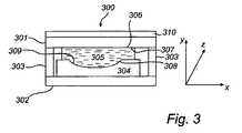
本発明による切替可能なレンズ300の一例が、図3の断面図によって示されている。このレンズ300はともにセルを形成する2つの基板301,302を有しており、これらの基板はスペーサ素子303により封止されている。上記セルは、正の異方性を持つ(ne>no)液晶混合物305と、この液晶混合物305との界面を成す凹面を持つ固体ポリマ体305とを有している。上記各基板には透明電極306,308が設けられており、上記液晶の各界面には配向層307,309が配されている。上記各配向層は、平行であり好ましくは反対のラビング方向を有しており、液晶層における一軸配向を引き起こす。この目的のために、上記液晶混合物は、ネマティック層にあるように選択されることが好ましい。説明上の理由のために、図3に3次元の座標系が示されている。この座標系を参照すると、上記基板はXZ平面に延在し、Y軸方向は光路(すなわち光軸)を規定する。平坦な配向層307はX方向にラビングされ、その場合、凹形の配向層309は反対のX軸方向にラビングされ得る。電極308は、代替として平坦な基板302の上に直接配されてもよい。An example of a
(Y軸方向に)レンズを通って進み、ラビング方向に沿って(すなわちX軸方向に沿って)直線偏光を持つ光は、液晶の異常光の屈折率neに等しい液晶の有効屈折率neffを経験する。しかしながら、液晶分子がXZ平面から傾斜している場合には、直線偏光光により経験される有効屈折率は、通常光の屈折率noに向かって徐々に変化する。液晶分子が90°傾斜している場合、及び従って液晶分子と平行である場合には、有効屈折率はnoに等しい。Travels through the (Y axis direction) lens, along a rubbing direction (i.e. along the X-axis direction) light having a linearly polarized light, the liquid crystal of the abnormal effective refractive index of the liquid crystal is equal to the refractive index ne of the light n Experienceeff . However, if the liquid crystal molecules are tilted from the XZ plane, the effective refractive index experienced by the linearly polarized light is changed gradually to the refractive index no of the ordinary light. If the liquid crystal molecules are inclined 90 °, and therefore when it is parallel to the liquid crystal molecules, the effective refractive index is equal to no.
上記有効屈折率は、
液晶が凸形状を有し、固体ポリマ体が凹形状を有する場合、レンズ形状のポリマ体と液晶の層との間に半径Rの球面上の界面(すなわち球形のレンズ面)を持つ液晶レンズの焦点距離は、
fLC=R/(neff−ni)
により与えられる。ここで、niは凹状のポリマ体の(等方性)屈折率である。When the liquid crystal has a convex shape and the solid polymer body has a concave shape, a liquid crystal lens having a spherical surface of radius R (ie, a spherical lens surface) between the lens-shaped polymer body and the liquid crystal layer. The focal length is
fLC = R / (neff −ni )
Given by. Here, ni is the (isotropic) refractive index of the concave polymer body.
しかしながら、X軸方向に沿って直線偏光されていない光は、屈折率のシフトを経験しない。従って、そのような光は、静的であり、液晶分子のいかなる傾斜にも依存しないものとしてレンズを認識する。実際には、そのような光は、常にnoに等しい屈折率を経験する。固体の凹体がnoに等しい等方性屈折率を持つ材料から形成されている場合には、そのような光は実際にはレンズを通って影響を受けることなく進む。However, light that is not linearly polarized along the X-axis direction does not experience a refractive index shift. Therefore, such light recognizes the lens as being static and independent of any tilt of the liquid crystal molecules. In fact, such light will always experience a refractive index equal to no. If the solid concave body is formed from a material having the same isotropic refractive index no, such light travels without being affected through the actually lens.
必要な偏光を与えるために、典型的にはレンズ構造体300の上に直線偏光子310が設けられる。しかしながら、通常の偏光子は、光を吸収し、正しくない偏光を持つ任意の光線を吸収することにより光を偏光する。実際にはランダムな偏光光の50%が典型的には偏光子により吸収され、かなり低減された明るさをもたらす。 A
従って、他の実施の形態によれば、上記レンズは、図4の断面図により模式的に示されているように各偏光方向に対して1つの、2つの重ね合わされた液晶セルを備えている。この目的のために、上記レンズは、配向層のラビング方向のみセル404とは異なる追加の液晶セル405を備え得る。従って、レンズは、図3に示されているレンズの全ての素子を別個に有する2つのレンズ部401,402を有する。しかしながら、上記2つのレンズ部は、1つの共通基板403を共有してもよく、好ましくは(それぞれX軸方向及びZ軸方向に)互いに垂直に配向された対応する液晶をもつべきである。原則的に、基板のサイドのうち直接的又はポリマ体を介して間接的に液晶と対向する各サイドは、4つの電極を得るような分離した電極を備え得る。中央の電極は、各電極に短配線することにより共有の共通電極として機能する。ある好適な材料の場合、共通基板403の2つの電極が単一のサイド上の1つの電極のみに取り替えられ得る。1つのセル(404又は405)の場合、電界は基板を透過する。共通電極403に配された少なくとも1つの電極は、セルの個々のスイッチングを与え、両方の偏光の光に対して正確な集束作用を可能にする。 Thus, according to another embodiment, the lens comprises two superimposed liquid crystal cells, one for each polarization direction, as schematically illustrated by the cross-sectional view of FIG. . For this purpose, the lens may comprise an additional
基本的には、全ての光は2つのレンズのうちの1つのみにより影響を及ぼされるので、垂直な分子の配向を持つ2つの重ね合わされたセルは、偏光に依存しないレンズをもたらす。しかしながら、鮮明な画像を与えるため、各レンズは、光路内の各レンズ部の異なる場所のためにわずかに異なる焦点距離を補償するようわずかに異なる曲率及び/又は屈折率の差を与えられなければならないかもしれない。 Basically, since all the light is affected by only one of the two lenses, two superimposed cells with perpendicular molecular orientation result in a polarization independent lens. However, in order to provide a clear image, each lens must be given a slightly different curvature and / or refractive index difference to compensate for slightly different focal lengths due to different locations of each lens section in the optical path. It may not be.
上述したように、好ましくはレンズはできる限り小型であるべきである。この目的のために、上記偏光に依存しないレンズは、共通基板403を取り除き、代わりに図5に示されているような設計を用いることにより更に簡素化され得る。この実施の形態によれば、レンズ500は、2つの基板502,502と、専ら1つの(共通の)固体レンズ体501とを有している。図示されている共通レンズ体501は、各液晶層504,505に凸形の界面を与える楕円形状を有している。上記レンズは各基板502,503に1つの電極、よって2つの電極のみを必要とし、これらは一緒に両方の液晶層にわたって1つの共通の電界を与える。勿論、凹形の界面が望まれる場合には、楕円形状は両凹形状に置き換えられ得る。楕円形状又は両凹形状が用いられる場合、一方の混合物の有効屈折率がポリマ体の屈折率よりも高く、他方の液晶混合物の有効屈折率がポリマ体の屈折率よりも低くなるように、2つのセルの液晶混合物は好ましくは異なるべきである。それにより、2つのレンズ部の集束作用は同じ符号及び大きさ(正又は負のいずれか一方)を持つ。勿論、代替の解決策は、1つの凹面と1つの凸面とを持つポリマ体を用いることである。それにより、両方のレンズ部に関して同じ液晶混合物が用いられる一方で、2つのレンズ部において一致する光集束作用(正又は負)を維持する。 As mentioned above, preferably the lens should be as small as possible. For this purpose, the polarization independent lens can be further simplified by removing the
図5に示されている実施の形態では、2つの電極のみが存在する。従って、各セルは個々に調整され得ない。個々のアドレスの可能性と比較して、2つのセルに関する部分的に重なる焦点を確実にするためにレンズ体501の曲面の正確な設計及び形状がより重要である。 In the embodiment shown in FIG. 5, there are only two electrodes. Therefore, each cell cannot be adjusted individually. Compared to the possibility of individual addresses, the exact design and shape of the curved surface of the
上記レンズ積層体は、例えば調節可能な焦点深度及び調節可能な電界の深さを与える多くの異なる構成を持つことが可能である。原則的に、(可動レンズを備えた)既存の構成に対して動作する任意の構成も、本明細書において述べられる液晶レンズとともに用いられ得る。液晶レンズを用いる2つの大きな利点は、組立の高さが低減され得ること及び可動部品が不要であることである。 The lens stack can have many different configurations, for example providing an adjustable depth of focus and an adjustable electric field depth. In principle, any configuration that operates on an existing configuration (with a movable lens) can also be used with the liquid crystal lenses described herein. Two major advantages of using liquid crystal lenses are that assembly height can be reduced and no moving parts are required.
調節可能な電界の深さを与えるズームレンズは少なくとも2つのレンズを要し、1つのレンズは正の屈折力を持ち、1つのレンズは負の屈折率を持ち、これらはともに望遠鏡設備(setup)を形成する。 A zoom lens providing an adjustable electric field depth requires at least two lenses, one lens having positive refractive power and one lens having a negative refractive index, both of which are telescope setups. Form.
正のレンズと負のレンズとの組み合わせは、電界の深さ及び従ってズーム力を大きく又は小さくする一方で、全ての画像の場所において光軸と平行な画像を維持する。 The combination of positive and negative lenses increases or decreases the depth of the electric field and thus the zooming power, while maintaining an image parallel to the optical axis at all image locations.
明らかに、ほとんどのレンズ積層体は、1つ(又は複数)の調節可能なレンズだけではなく、固定された焦点を持つ幾つかのレンズも有している。そのようなレンズは、上記調節可能な液晶レンズにおけるレンズ形状の物体と同様に形成され得る。 Obviously, most lens stacks have not only one (or more) adjustable lenses, but also some lenses with a fixed focus. Such a lens can be formed similarly to the lens-shaped object in the adjustable liquid crystal lens.
上述したような可変焦点レンズは、2つの連続する工程段階において製造され得る。第1の工程段階では、図6に示されているような以下の工程を含む光複製プロセスにより固体の物体が製造され得る。
1.型601が所定の位置にもたらされ、光重合された生成物をこの型から容易にはずすことができるように処理されるとともに、透明導体を支持する透明基板602が準備される。
2.基板602の上又は型601の内部に少量のモノマ603が与えられる。このモノマ603は、最終生成物の内部におけるいかなる気泡の発生をも防止するために脱気されることが好ましく、更に少量の光開始剤と混合される。
3.型601と基板602とが接合され、任意の過剰のモノマがその結果得られる穴部から押し出される。実際には、上記モノマは、型と基板との間に挟まれる。
4.その後、上記モノマは、紫外光604に曝され、重合する。紫外光604は、基板602を介して又は透明な型が用いられる場合には型601を介してモノマ603に入る。しかしながら、例えば熱を用いる代替の重合プロセスが等しく可能である。そのような場合には、光開始剤が典型的には省略されるか、又は他の好適な開始剤に取り替えられる。
5.重合されると、型のわずかな曲げにより又は衝撃パルスにより固体605は型からはずされ得る。A variable focus lens as described above can be manufactured in two successive process steps. In the first process step, a solid object can be produced by an optical replication process including the following steps as shown in FIG.
1. A
2. A small amount of
3. The
4). Thereafter, the monomer is exposed to
5). Once polymerized, solid 605 can be removed from the mold by slight bending of the mold or by shock pulses.
第2の工程段階では、上記第1の工程段階において準備された固体の物体が、図7に従って部品を完成させるために用いられる。第2の工程段階は、以下のステップを含んでいる。
1.固体レンズ体605に配向層が与えられる。この配向層は、そのような使用に好適な任意の利用可能な材料、例えばポリイミドから形成され得る。ポリイミドが用いられる場合には、その溶液が例えばスピンコートされ、高温(例えば90℃)で乾燥させた後布地を用いてラビングされる。
2.第2の透明電極を支持する第2の透明基板606は、第2の配向層を備える。ここでは、固体レンズ体605に関してと同じ材料及び使用技術(application technique)が用いられ得る。しかしながら、上記基板は、典型的にはガラスから形成されており、従って配向層の硬化のためのかなり強力な熱処理(例えば180℃)に耐性があり、より急速な硬化プロセスを可能にする。
3.その後、正しいアライメントを確実にするために接着剤とスペーサ素子607とを用いて固体レンズ体605と第2の基板606とが接合される。平行な液晶分子の配向が望まれる場合には、上記素子は各配向層と平行に接続される。しかしながら、ねじれ配向が代替として可能であり、これは互いに対して配向層を90°回転させることにより与えられる。スペーサ素子607は、分離した素子であってもよいし、基板又はポリマ体のいずれか一方に一体化されてもよい。
4.上記セルは、最後に液晶分子608で満たされ、封止される。充填は、自然に発生する毛管力のために典型的には非常に容易であり、接着剤の液滴が封止を与える。In the second process stage, the solid object prepared in the first process stage is used to complete the part according to FIG. The second process stage includes the following steps.
1. An alignment layer is provided on the
2. The second
3. Thereafter, in order to ensure correct alignment, the
4). The cell is finally filled with
2つのレンズ部を持つ偏光に影響を受けないレンズが望まれる場合には、典型的には第2の部分のための開始基板として第1の部分の基板を用いて上記各工程がもう一度繰り返される。各レンズ部のために分離した電極が必要とされる場合には、勿論当該基板は各サイドに1つの電極層を持つ必要がある。 If a polarization-insensitive lens with two lens parts is desired, the above steps are repeated once, typically using the first part substrate as the starting substrate for the second part. . If separate electrodes are required for each lens part, of course, the substrate needs to have one electrode layer on each side.
図5に示されているようなレンズが望まれる場合には、2つの型の間においてモノマが圧搾され得る。両方の型は、重合された物体を容易にはずすことができるように処理されなければならない。その後、両方のレンズの表面がアライメント層、例えば液晶層の垂直な配向を与えるように垂直にラビングされたポリイミドとともに配される。続いて、接着剤及びスペーサ素子を用いるが液晶混合物を注入するための小さな穴部を残して、それぞれ電極とラビングされたアライメント層とを備えた2つの基板の間にポリマ体が配される。その後、2つのセルが液晶で満たされ、最後に接着剤の液滴がセルを閉じるために用いられる。 If a lens as shown in FIG. 5 is desired, the monomer can be squeezed between the two molds. Both molds must be treated so that the polymerized object can be easily removed. Thereafter, the surfaces of both lenses are placed with an alignment layer, eg, a polyimide that is rubbed vertically to give a vertical orientation of the liquid crystal layer. Subsequently, a polymer body is placed between two substrates, each using an electrode and a rubbed alignment layer, using an adhesive and a spacer element, but leaving a small hole for injecting the liquid crystal mixture. The two cells are then filled with liquid crystal and finally a drop of adhesive is used to close the cell.
一般に、ポリマ体において架橋されたポリマ鎖を得ることが大いに望ましく、これは化学薬品及び熱劣化に曝された際に当該ポリマ体をより安定にする。上述したように、ポリマ体は光開始剤及び紫外光を用いて与えられ得る。しかしながら、ポリマ体を重合する代替のやり方が使用され得る。この目的のために、2つの主要な重合メカニズムが確認されている。第1の反応は、フリーラジカル光開始剤を用いるフリーラジカルにより開始される重合メカニズムにより与えられ、第2の反応は、典型的にはルイス酸の使用により開始されるカチオン重合メカニズムにより与えられる。上記フリーラジカルのメカニズムに適した限定されない種類のモノマは、(メタ)アクリレート及びビニルモノマよりなる群に含まれる。そのようなモノマの1つの例は、2,2−ビス[4−(2−ヒドロキシ−3−アクリロイルプロポキシ)フェニル]プロパン(Bis-GAA)である。上記カチオン反応メカニズムのために、エポキシド,オキセタン及びビニルエーテルモノマが用いられ得る。そのようなモノマの1つの例は、ビスフェノール−Aのジグリシドエーテルである。 In general, it is highly desirable to obtain crosslinked polymer chains in the polymer body, which makes the polymer body more stable when exposed to chemicals and thermal degradation. As described above, the polymer body can be provided using a photoinitiator and ultraviolet light. However, alternative ways of polymerizing the polymer body can be used. For this purpose, two main polymerization mechanisms have been identified. The first reaction is provided by a free radical initiated polymerization mechanism using a free radical photoinitiator, and the second reaction is typically provided by a cationic polymerization mechanism initiated by use of a Lewis acid. Non-limiting types of monomers suitable for the free radical mechanism are included in the group consisting of (meth) acrylates and vinyl monomers. One example of such a monomer is 2,2-bis [4- (2-hydroxy-3-acryloylpropoxy) phenyl] propane (Bis-GAA). For the cationic reaction mechanism, epoxides, oxetanes and vinyl ether monomers can be used. One example of such a monomer is the diglycidic ether of bisphenol-A.
上述したモノマは、全て熱重合され得る。好適な開始剤を用いると、室温に近い温度で十分である。 All of the above monomers can be thermally polymerized. With a suitable initiator, a temperature close to room temperature is sufficient.
上述したように、モノマは重合開始剤も含んでいてもよい。開始剤はフリーラジカル開始剤又は酸発生器であり得る。熱的かつ電磁的な放射(例えば紫外線の放射)により活性化され得る単一の開始剤が用いられることが好ましい。アゾビスイソブチロニトリルが1つの実現可能な例であるが、多くのアゾエステルも用いられ得る。アゾエステル開始剤は、光化学的な分解は別として、かなり低温でかなり高い分解速度を持ち、低温及び単に少し高い温度でも当該開始剤を使用可能にするという利点を有する。 As described above, the monomer may also contain a polymerization initiator. The initiator can be a free radical initiator or an acid generator. It is preferred to use a single initiator that can be activated by thermal and electromagnetic radiation (eg ultraviolet radiation). Azobisisobutyronitrile is one feasible example, but many azo esters can also be used. Azoester initiators, apart from photochemical degradation, have the advantage of having a fairly high degradation rate at fairly low temperatures, allowing the initiator to be used at low temperatures and only slightly higher temperatures.
専らより高い温度で分解する実現可能な光開始剤の例は、イルガキュア184及びダロキュア1173(ともにチバガイギー株式会社の登録商標)のようなα−ヒドロキシ−ケトン、イルガキュア907及びイルガキュア369(ともにチバガイギー株式会社の登録商標)のようなα−アミノ−ケトン、イルガキュア651(=DMPA:α,α−ジメトキシ−α−フェニル−アセトフェノン)(チバガイギー株式会社の登録商標)のようなベンジルジメチル−ケタールである。 Examples of feasible photoinitiators that decompose exclusively at higher temperatures include α-hydroxy-ketones such as Irgacure 184 and Darocur 1173 (both are registered trademarks of Ciba Geigy Corporation), Irgacure 907 and Irgacure 369 (both Ciba Geigy Corporation). Α-amino-ketone such as Irgacure 651 (= DMPA: α, α-dimethoxy-α-phenyl-acetophenone) (registered trademark of Ciba Geigy Co., Ltd.).
上述した例は、全てフリーラジカル開始剤である。あるモノマのカチオン重合に好適な酸発生器の2つの種類、ジフェニルヨードニウム塩(例えばジフェニルヨードニウムヘキサフロロヒ酸塩)及びトリフェニルスルフォニウム塩(トリフェニルスルフォニウムヘキサフロロアンチモン酸塩)が存在する。これら2つの種類は、所謂ルイス酸であり、変形例は主に対イオンのタイプに見出される。2番目の種類(トリフェニルスルフォニウム塩)では、フェニル環の量も変化し、各フェニル環は硫黄の結合を介して互いに接続されている。 The examples described above are all free radical initiators. There are two types of acid generators suitable for cationic polymerization of certain monomers, diphenyliodonium salts (eg, diphenyliodonium hexafluoroarsenate) and triphenylsulfonium salts (triphenylsulfonium hexafluoroantimonate). These two types are so-called Lewis acids, and variants are mainly found in the counterion type. In the second type (triphenylsulfonium salt), the amount of phenyl rings also changes, and each phenyl ring is connected to each other via a sulfur bond.
一般的な光酸発生器に加えて、種々の塩又は塩の混合物も実現可能である。また、開始剤の吸収スペクトル又は効率をシフトさせるために促進剤が加えられてもよい。実現可能な促進剤の例は、アントラセン又はチオキサントンを含んでいる。 In addition to common photoacid generators, various salts or mixtures of salts are also feasible. Accelerators may also be added to shift the absorption spectrum or efficiency of the initiator. Examples of possible promoters include anthracene or thioxanthone.
要するに、本発明は、調節可能な焦点深度を与える液晶をベースとするレンズを使用する例えば携帯電話に用いられるようなカメラ装置に関連している。このカメラ装置は、固定された単一的な(unitary)装置に配されたフォトセンサ201のアレイと、少なくとも2つのレンズ202,203,204とを有している。レンズのうちの少なくとも1つ202は、当該レンズにおいて調節可能な焦点距離を与える液晶層101を有している。その他のレンズ203,204は、用途に依存して固定された又は調節可能な焦点距離を持つ。一実施の形態によれば、上記カメラ装置は、少なくとも1つの追加の調節可能なレンズを有し、各レンズは、調節可能な焦点深度及び調節可能な電界の深さを与えるように配される。 In short, the present invention relates to a camera device, such as used in a mobile phone, which uses a liquid crystal based lens that provides an adjustable depth of focus. This camera device has an array of
Claims (17)
Translated fromJapanese第1のアライメント面と第2のアライメント面とを有する第1の液晶セルであって、前記アライメント面のうちの少なくとも1つがポリマ体により規定されるレンズ形状の面であり、異方性の屈折率を持ち、予め規定された分子の配向が引き起こされるように前記アライメント面の間に配された液晶分子の層を更に有する当該第1の液晶セルと、
前記液晶分子の層の両サイドに設けられ、与えられる電界によって前記液晶分子の層における屈折率を制御するように作用する電極のペアと
を有するカメラ装置であって、
前記レンズは、当該カメラ装置が調節可能な焦点深度を持つように前記固定された構成において配されている当該カメラ装置。Integrally having at least two lenses and a photosensor array in a fixed configuration forming one unit, the first of the lenses having an adjustable focal length;
A first liquid crystal cell having a first alignment surface and a second alignment surface, wherein at least one of the alignment surfaces is a lens-shaped surface defined by a polymer body, and anisotropic refraction The first liquid crystal cell having a ratio and further comprising a layer of liquid crystal molecules disposed between the alignment surfaces so as to cause a predefined molecular orientation;
A pair of electrodes provided on both sides of the liquid crystal molecule layer and acting to control a refractive index in the liquid crystal molecule layer by an applied electric field,
The camera device, wherein the lens is arranged in the fixed configuration so that the camera device has an adjustable depth of focus.
前記形成する工程は、
レンズ形状のモノマ体が第1の基板に形成されるように、前記第1の基板と型との間にモノマを配する工程と、
前記モノマを重合する工程であって、それにより前記第1の基板にレンズ形状のポリマ体を形成する当該工程と、
前記ポリマ体から前記型を取り除く工程と、
前記ポリマ体にアライメント層を配する工程と、
アライメント層を備えた第2の基板を与える工程と、
前記第1及び前記第2の基板に電極を配する工程と、
前記ポリマ体と前記第2の基板との間に液晶分子の層を挟む工程であって、それにより調節可能な焦点距離を持つレンズを形成する当該工程と
を有し、当該方法が、
第2のレンズを与える工程と、
フォトセンサアレイを与える工程と、
調節可能な焦点深度が前記カメラ装置において与えられるように1つのユニットを形成する固定された構成において前記第1のレンズ、第2のレンズ及びフォトセンサアレイを配列する工程と
を更に有する当該カメラ装置の製造方法。A method of manufacturing a camera device, comprising: forming a first lens having an adjustable focal length and having liquid crystal molecules,
The forming step includes
Disposing a monomer between the first substrate and the mold so that a lens-shaped monomer body is formed on the first substrate;
Polymerizing the monomer, thereby forming a lens-shaped polymer body on the first substrate; and
Removing the mold from the polymer body;
Arranging an alignment layer on the polymer body;
Providing a second substrate with an alignment layer;
Disposing electrodes on the first and second substrates;
A step of sandwiching a layer of liquid crystal molecules between the polymer body and the second substrate, thereby forming a lens having an adjustable focal length, and the method comprises:
Providing a second lens;
Providing a photosensor array;
Arranging the first lens, the second lens, and the photosensor array in a fixed configuration that forms a unit such that an adjustable depth of focus is provided in the camera device. Manufacturing method.
Applications Claiming Priority (2)
| Application Number | Priority Date | Filing Date | Title |
|---|---|---|---|
| EP04100449 | 2004-02-06 | ||
| PCT/IB2005/050270WO2005076069A1 (en) | 2004-02-06 | 2005-01-24 | Camera arrangement, mobile phone comprising a camera arrangement, method of manufacturing a camera arrangement |
Publications (1)
| Publication Number | Publication Date |
|---|---|
| JP2007528506Atrue JP2007528506A (en) | 2007-10-11 |
Family
ID=34833740
Family Applications (1)
| Application Number | Title | Priority Date | Filing Date |
|---|---|---|---|
| JP2006551962AWithdrawnJP2007528506A (en) | 2004-02-06 | 2005-01-24 | Camera device, mobile phone having camera device, and method of manufacturing camera device |
Country Status (6)
| Country | Link |
|---|---|
| US (1) | US20080252769A1 (en) |
| EP (1) | EP1711860A1 (en) |
| JP (1) | JP2007528506A (en) |
| KR (1) | KR20060124687A (en) |
| CN (1) | CN1914555A (en) |
| WO (1) | WO2005076069A1 (en) |
Cited By (3)
| Publication number | Priority date | Publication date | Assignee | Title |
|---|---|---|---|---|
| WO2009072748A1 (en)* | 2007-12-04 | 2009-06-11 | Hysonic.Co., Ltd. | Camera module using polymer metal composite |
| JP2009528558A (en)* | 2006-03-03 | 2009-08-06 | ユニヴェルシテ ラヴァル | Method and apparatus for generating spatially modulated electric fields and electro-optical tuning using liquid crystals |
| KR100943439B1 (en) | 2007-12-04 | 2010-02-19 | 주식회사 하이소닉 | Camera Module Using Polymer Metal Composite |
Families Citing this family (26)
| Publication number | Priority date | Publication date | Assignee | Title |
|---|---|---|---|---|
| WO2008011003A2 (en)* | 2006-07-17 | 2008-01-24 | Tessera North America, Inc. | Camera system and associated methods |
| KR101228851B1 (en) | 2005-05-20 | 2013-02-01 | 코닌클리케 필립스 일렉트로닉스 엔.브이. | Electrowetting element, lens system, electronic device and driving method |
| KR100759510B1 (en)* | 2006-03-08 | 2007-09-18 | 삼성전기주식회사 | Liquid lens |
| WO2008087486A2 (en)* | 2006-09-14 | 2008-07-24 | Tessera Technologies Hungary Kft. | Imaging system with improved image quality and associated methods |
| EP2069851A4 (en)* | 2006-09-14 | 2010-02-24 | Tessera Tech Hungary Kft | IMAGING SYSTEM WITH ASSOUPLY ASSEMBLED TOLERANCES AND ASSOCIATED METHODS |
| CN101153945A (en) | 2006-09-29 | 2008-04-02 | 鸿富锦精密工业(深圳)有限公司 | Lens module |
| CN101419323A (en)* | 2007-10-22 | 2009-04-29 | 鸿富锦精密工业(深圳)有限公司 | Mini camera module and method for producing the same |
| CN101458346B (en)* | 2007-12-11 | 2011-05-04 | 鸿富锦精密工业(深圳)有限公司 | Liquid lens |
| US8699141B2 (en) | 2009-03-13 | 2014-04-15 | Knowles Electronics, Llc | Lens assembly apparatus and method |
| US8659835B2 (en) | 2009-03-13 | 2014-02-25 | Optotune Ag | Lens systems and method |
| WO2010129460A1 (en)* | 2009-05-03 | 2010-11-11 | Lensvector Inc. | Camera module with tolerance adjustment using embedded active optics |
| CN101931742B (en)* | 2009-06-18 | 2013-04-24 | 鸿富锦精密工业(深圳)有限公司 | Image sensing module and image capture module |
| TWI426305B (en)* | 2009-06-22 | 2014-02-11 | Hon Hai Prec Ind Co Ltd | Image sensing module and image capturing module |
| JP2011180293A (en)* | 2010-02-26 | 2011-09-15 | Fujifilm Corp | Lens array |
| US20110221950A1 (en)* | 2010-03-12 | 2011-09-15 | Doeke Jolt Oostra | Camera device, wafer scale package |
| US9239494B2 (en)* | 2011-11-09 | 2016-01-19 | Lachezar Komitov | Polymer network stabilized flexoelectric polarization |
| US9715612B2 (en)* | 2012-12-26 | 2017-07-25 | Cognex Corporation | Constant magnification lens for vision system camera |
| CN103969857B (en)* | 2014-05-23 | 2017-09-15 | 豪威光电子科技(上海)有限公司 | Wafer scale zoom lens module and preparation method thereof |
| US9366879B1 (en) | 2014-12-02 | 2016-06-14 | Hutchinson Technology Incorporated | Camera lens suspension with polymer bearings |
| US9454016B1 (en) | 2015-03-06 | 2016-09-27 | Hutchinson Technology Incorporated | Camera lens suspension with integrated electrical leads |
| JP6923563B2 (en) | 2016-06-09 | 2021-08-18 | ハッチンソン テクノロジー インコーポレイテッドHutchinson Technology Incorporated | Shape memory alloy wire mounting structure with adhesive for suspension assembly |
| US11050944B2 (en) | 2018-11-29 | 2021-06-29 | Microsoft Technology Licensing, Llc | Switched polarization imaging to detect display screen |
| US10924645B2 (en) | 2018-11-29 | 2021-02-16 | Microsoft Technology Licensing, Llc | Polarization imaging to detect display screen |
| CN110867136B (en)* | 2019-11-22 | 2021-10-15 | 维沃移动通信有限公司 | Pole screen and electronic equipment |
| CN113678059B (en)* | 2020-06-30 | 2023-05-16 | 深圳市大疆创新科技有限公司 | Tripod head camera and shell and movable platform thereof |
| TWI817157B (en)* | 2021-07-07 | 2023-10-01 | 鮑威源 | Optical chamberr for outputting light beam with controlled orientation |
Family Cites Families (15)
| Publication number | Priority date | Publication date | Assignee | Title |
|---|---|---|---|---|
| US3278654A (en)* | 1958-04-25 | 1966-10-11 | Lentilles Ophtalmiques Special | Apparatus and method of producing optical and ophthalmic lenses from thermosetting resin materials |
| US2964501A (en)* | 1960-04-13 | 1960-12-13 | Titmus Optical Company Inc | Glycol carbonate addition polymers |
| US3211811A (en)* | 1964-06-29 | 1965-10-12 | Armorlite Leus Company Inc | Method and apparatus for casting thermosetting plastic lenses |
| US3605195A (en)* | 1970-08-24 | 1971-09-20 | Charles D Campbell | Mold assembly for casting plastic optical lenses |
| US3902693A (en)* | 1973-03-12 | 1975-09-02 | American Optical Corp | Mold for casting lenses |
| US4197266A (en)* | 1974-05-06 | 1980-04-08 | Bausch & Lomb Incorporated | Method for forming optical lenses |
| JPS62170934A (en)* | 1986-01-24 | 1987-07-28 | Olympus Optical Co Ltd | Liquid crystal lens |
| US5150234A (en)* | 1988-08-08 | 1992-09-22 | Olympus Optical Co., Ltd. | Imaging apparatus having electrooptic devices comprising a variable focal length lens |
| US5097352A (en)* | 1988-09-28 | 1992-03-17 | Olympus Optical Co., Ltd. | Optical system including liquid crystal devices |
| JP2612914B2 (en)* | 1988-10-19 | 1997-05-21 | オリンパス光学工業株式会社 | Optical system with multiple liquid crystal elements |
| JPH03167519A (en)* | 1989-11-27 | 1991-07-19 | Sekisui Chem Co Ltd | Production of liquid crystal lens |
| US5160749A (en)* | 1990-10-30 | 1992-11-03 | Minnesota Mining And Manufacturing Company | Three piece mold assembly for making an ocular device |
| JPH1073758A (en)* | 1996-06-07 | 1998-03-17 | Olympus Optical Co Ltd | Image forming optical system |
| US6437925B1 (en)* | 1998-06-30 | 2002-08-20 | Olympus Optical Co., Ltd. | Optical apparatus |
| JP2002094955A (en)* | 2000-02-22 | 2002-03-29 | Philips Japan Ltd | Image display and pickup device |
- 2005
- 2005-01-24JPJP2006551962Apatent/JP2007528506A/ennot_activeWithdrawn
- 2005-01-24WOPCT/IB2005/050270patent/WO2005076069A1/ennot_activeApplication Discontinuation
- 2005-01-24EPEP05702761Apatent/EP1711860A1/ennot_activeWithdrawn
- 2005-01-24USUS10/597,608patent/US20080252769A1/ennot_activeAbandoned
- 2005-01-24KRKR1020067015643Apatent/KR20060124687A/ennot_activeWithdrawn
- 2005-01-24CNCNA2005800039693Apatent/CN1914555A/enactivePending
Cited By (3)
| Publication number | Priority date | Publication date | Assignee | Title |
|---|---|---|---|---|
| JP2009528558A (en)* | 2006-03-03 | 2009-08-06 | ユニヴェルシテ ラヴァル | Method and apparatus for generating spatially modulated electric fields and electro-optical tuning using liquid crystals |
| WO2009072748A1 (en)* | 2007-12-04 | 2009-06-11 | Hysonic.Co., Ltd. | Camera module using polymer metal composite |
| KR100943439B1 (en) | 2007-12-04 | 2010-02-19 | 주식회사 하이소닉 | Camera Module Using Polymer Metal Composite |
Also Published As
| Publication number | Publication date |
|---|---|
| WO2005076069A1 (en) | 2005-08-18 |
| EP1711860A1 (en) | 2006-10-18 |
| US20080252769A1 (en) | 2008-10-16 |
| CN1914555A (en) | 2007-02-14 |
| KR20060124687A (en) | 2006-12-05 |
Similar Documents
| Publication | Publication Date | Title |
|---|---|---|
| JP2007528506A (en) | Camera device, mobile phone having camera device, and method of manufacturing camera device | |
| CN102252223B (en) | Lighting device and display device | |
| US7446830B2 (en) | Method for aligning polymer network liquid crystal | |
| US11644698B2 (en) | Electrically controllable optical element, in particular thin-film cell having an optically active surface profile, and method for the production thereof | |
| TWI250327B (en) | Reflecting board, liquid crystal device and electronic device | |
| EP2064590B1 (en) | Curvature reduction for switchable liquid crystal lens array | |
| US20110221950A1 (en) | Camera device, wafer scale package | |
| US20120113318A1 (en) | Methods of Adjustment Free Manufacture Of Focus Free Camera Modules | |
| JP5533780B2 (en) | Liquid crystal lens structure and driving method thereof | |
| CN111194425B (en) | Flexible liquid crystal cell and lens | |
| CN109328312B (en) | Active lens structure and method for manufacturing the same | |
| KR20130024863A (en) | Liquid crystal cell | |
| AU2021245170A1 (en) | Flexible, adjustable lens power liquid crystal cells and lenses | |
| CN102540316A (en) | Method of fabricating patterned retarder | |
| KR102490632B1 (en) | Liquid crystal display device having polarizing plate and method for fabricating the same | |
| JP2019501424A (en) | Electrically controllable optical element consisting of an optically isotropic liquid, in particular a lens, and its manufacturing method based on a liquid composite material | |
| CN103091927B (en) | A kind of Schema control cascade connection type liquid crystal microlens array | |
| KR102263949B1 (en) | Structure and fabrication method of active switching random-refraction device to control field of view and coherency of light | |
| KR101851780B1 (en) | Method of fabricating patterned retarder | |
| Ren et al. | 62.1: Invited Paper: Liquid Crystal and Liquid Lenses for Displays and Image Processing | |
| CN120677428A (en) | Optical laminate and image display device | |
| HK40022393A (en) | Electrically controllable optical element, in particular thin-film cell having an optically active surface profile, and method for the production thereof | |
| HK40045253B (en) | Flexible, adjustable lens power liquid crystal cells and lenses | |
| HK40045253A (en) | Flexible, adjustable lens power liquid crystal cells and lenses | |
| KR20130067878A (en) | Polymer dispersed liquid crystal lenz |
Legal Events
| Date | Code | Title | Description |
|---|---|---|---|
| A300 | Application deemed to be withdrawn because no request for examination was validly filed | Free format text:JAPANESE INTERMEDIATE CODE: A300 Effective date:20080401 |