JP2007525858A - Printed circuit device with integrated antenna and implantable sensor processing device with printed integrated circuit board antenna - Google Patents
Printed circuit device with integrated antenna and implantable sensor processing device with printed integrated circuit board antennaDownload PDFInfo
- Publication number
- JP2007525858A JP2007525858AJP2006509990AJP2006509990AJP2007525858AJP 2007525858 AJP2007525858 AJP 2007525858AJP 2006509990 AJP2006509990 AJP 2006509990AJP 2006509990 AJP2006509990 AJP 2006509990AJP 2007525858 AJP2007525858 AJP 2007525858A
- Authority
- JP
- Japan
- Prior art keywords
- printed circuit
- substrate
- sensor device
- circuit device
- coil
- Prior art date
- Legal status (The legal status is an assumption and is not a legal conclusion. Google has not performed a legal analysis and makes no representation as to the accuracy of the status listed.)
- Pending
Links
Images


Classifications
- A—HUMAN NECESSITIES
- A61—MEDICAL OR VETERINARY SCIENCE; HYGIENE
- A61B—DIAGNOSIS; SURGERY; IDENTIFICATION
- A61B5/00—Measuring for diagnostic purposes; Identification of persons
- A61B5/145—Measuring characteristics of blood in vivo, e.g. gas concentration or pH-value ; Measuring characteristics of body fluids or tissues, e.g. interstitial fluid or cerebral tissue
- A61B5/1455—Measuring characteristics of blood in vivo, e.g. gas concentration or pH-value ; Measuring characteristics of body fluids or tissues, e.g. interstitial fluid or cerebral tissue using optical sensors, e.g. spectral photometrical oximeters
- A61B5/14551—Measuring characteristics of blood in vivo, e.g. gas concentration or pH-value ; Measuring characteristics of body fluids or tissues, e.g. interstitial fluid or cerebral tissue using optical sensors, e.g. spectral photometrical oximeters for measuring blood gases
- A61B5/14556—Measuring characteristics of blood in vivo, e.g. gas concentration or pH-value ; Measuring characteristics of body fluids or tissues, e.g. interstitial fluid or cerebral tissue using optical sensors, e.g. spectral photometrical oximeters for measuring blood gases by fluorescence
- G—PHYSICS
- G01—MEASURING; TESTING
- G01N—INVESTIGATING OR ANALYSING MATERIALS BY DETERMINING THEIR CHEMICAL OR PHYSICAL PROPERTIES
- G01N21/00—Investigating or analysing materials by the use of optical means, i.e. using sub-millimetre waves, infrared, visible or ultraviolet light
- G01N21/62—Systems in which the material investigated is excited whereby it emits light or causes a change in wavelength of the incident light
- G01N21/63—Systems in which the material investigated is excited whereby it emits light or causes a change in wavelength of the incident light optically excited
- G01N21/64—Fluorescence; Phosphorescence
- A—HUMAN NECESSITIES
- A61—MEDICAL OR VETERINARY SCIENCE; HYGIENE
- A61B—DIAGNOSIS; SURGERY; IDENTIFICATION
- A61B5/00—Measuring for diagnostic purposes; Identification of persons
- A—HUMAN NECESSITIES
- A61—MEDICAL OR VETERINARY SCIENCE; HYGIENE
- A61B—DIAGNOSIS; SURGERY; IDENTIFICATION
- A61B5/00—Measuring for diagnostic purposes; Identification of persons
- A61B5/0002—Remote monitoring of patients using telemetry, e.g. transmission of vital signals via a communication network
- A61B5/0031—Implanted circuitry
- A—HUMAN NECESSITIES
- A61—MEDICAL OR VETERINARY SCIENCE; HYGIENE
- A61B—DIAGNOSIS; SURGERY; IDENTIFICATION
- A61B5/00—Measuring for diagnostic purposes; Identification of persons
- A61B5/145—Measuring characteristics of blood in vivo, e.g. gas concentration or pH-value ; Measuring characteristics of body fluids or tissues, e.g. interstitial fluid or cerebral tissue
- A61B5/14532—Measuring characteristics of blood in vivo, e.g. gas concentration or pH-value ; Measuring characteristics of body fluids or tissues, e.g. interstitial fluid or cerebral tissue for measuring glucose, e.g. by tissue impedance measurement
- A—HUMAN NECESSITIES
- A61—MEDICAL OR VETERINARY SCIENCE; HYGIENE
- A61B—DIAGNOSIS; SURGERY; IDENTIFICATION
- A61B5/00—Measuring for diagnostic purposes; Identification of persons
- A61B5/145—Measuring characteristics of blood in vivo, e.g. gas concentration or pH-value ; Measuring characteristics of body fluids or tissues, e.g. interstitial fluid or cerebral tissue
- A61B5/1455—Measuring characteristics of blood in vivo, e.g. gas concentration or pH-value ; Measuring characteristics of body fluids or tissues, e.g. interstitial fluid or cerebral tissue using optical sensors, e.g. spectral photometrical oximeters
- A61B5/1459—Measuring characteristics of blood in vivo, e.g. gas concentration or pH-value ; Measuring characteristics of body fluids or tissues, e.g. interstitial fluid or cerebral tissue using optical sensors, e.g. spectral photometrical oximeters invasive, e.g. introduced into the body by a catheter
- A—HUMAN NECESSITIES
- A61—MEDICAL OR VETERINARY SCIENCE; HYGIENE
- A61B—DIAGNOSIS; SURGERY; IDENTIFICATION
- A61B5/00—Measuring for diagnostic purposes; Identification of persons
- A61B5/68—Arrangements of detecting, measuring or recording means, e.g. sensors, in relation to patient
- A61B5/6801—Arrangements of detecting, measuring or recording means, e.g. sensors, in relation to patient specially adapted to be attached to or worn on the body surface
- A61B5/6802—Sensor mounted on worn items
- A61B5/681—Wristwatch-type devices
- G—PHYSICS
- G01—MEASURING; TESTING
- G01N—INVESTIGATING OR ANALYSING MATERIALS BY DETERMINING THEIR CHEMICAL OR PHYSICAL PROPERTIES
- G01N21/00—Investigating or analysing materials by the use of optical means, i.e. using sub-millimetre waves, infrared, visible or ultraviolet light
- G01N21/62—Systems in which the material investigated is excited whereby it emits light or causes a change in wavelength of the incident light
- G01N21/63—Systems in which the material investigated is excited whereby it emits light or causes a change in wavelength of the incident light optically excited
- G01N21/64—Fluorescence; Phosphorescence
- G01N21/6428—Measuring fluorescence of fluorescent products of reactions or of fluorochrome labelled reactive substances, e.g. measuring quenching effects, using measuring "optrodes"
- G—PHYSICS
- G01—MEASURING; TESTING
- G01N—INVESTIGATING OR ANALYSING MATERIALS BY DETERMINING THEIR CHEMICAL OR PHYSICAL PROPERTIES
- G01N21/00—Investigating or analysing materials by the use of optical means, i.e. using sub-millimetre waves, infrared, visible or ultraviolet light
- G01N21/62—Systems in which the material investigated is excited whereby it emits light or causes a change in wavelength of the incident light
- G01N21/63—Systems in which the material investigated is excited whereby it emits light or causes a change in wavelength of the incident light optically excited
- G01N21/64—Fluorescence; Phosphorescence
- G01N21/645—Specially adapted constructive features of fluorimeters
- H—ELECTRICITY
- H05—ELECTRIC TECHNIQUES NOT OTHERWISE PROVIDED FOR
- H05K—PRINTED CIRCUITS; CASINGS OR CONSTRUCTIONAL DETAILS OF ELECTRIC APPARATUS; MANUFACTURE OF ASSEMBLAGES OF ELECTRICAL COMPONENTS
- H05K1/00—Printed circuits
- H05K1/16—Printed circuits incorporating printed electric components, e.g. printed resistor, capacitor, inductor
- H05K1/165—Printed circuits incorporating printed electric components, e.g. printed resistor, capacitor, inductor incorporating printed inductors
- G—PHYSICS
- G01—MEASURING; TESTING
- G01N—INVESTIGATING OR ANALYSING MATERIALS BY DETERMINING THEIR CHEMICAL OR PHYSICAL PROPERTIES
- G01N2201/00—Features of devices classified in G01N21/00
- G01N2201/12—Circuits of general importance; Signal processing
- G01N2201/124—Sensitivity
- G01N2201/1244—Ambient light detector, e.g. for invalidating
- H—ELECTRICITY
- H05—ELECTRIC TECHNIQUES NOT OTHERWISE PROVIDED FOR
- H05K—PRINTED CIRCUITS; CASINGS OR CONSTRUCTIONAL DETAILS OF ELECTRIC APPARATUS; MANUFACTURE OF ASSEMBLAGES OF ELECTRICAL COMPONENTS
- H05K1/00—Printed circuits
- H05K1/02—Details
- H05K1/03—Use of materials for the substrate
- H05K1/0306—Inorganic insulating substrates, e.g. ceramic, glass
- H—ELECTRICITY
- H05—ELECTRIC TECHNIQUES NOT OTHERWISE PROVIDED FOR
- H05K—PRINTED CIRCUITS; CASINGS OR CONSTRUCTIONAL DETAILS OF ELECTRIC APPARATUS; MANUFACTURE OF ASSEMBLAGES OF ELECTRICAL COMPONENTS
- H05K2201/00—Indexing scheme relating to printed circuits covered by H05K1/00
- H05K2201/08—Magnetic details
- H05K2201/083—Magnetic materials
- H05K2201/086—Magnetic materials for inductive purposes, e.g. printed inductor with ferrite core
- H—ELECTRICITY
- H05—ELECTRIC TECHNIQUES NOT OTHERWISE PROVIDED FOR
- H05K—PRINTED CIRCUITS; CASINGS OR CONSTRUCTIONAL DETAILS OF ELECTRIC APPARATUS; MANUFACTURE OF ASSEMBLAGES OF ELECTRICAL COMPONENTS
- H05K2201/00—Indexing scheme relating to printed circuits covered by H05K1/00
- H05K2201/09—Shape and layout
- H05K2201/09818—Shape or layout details not covered by a single group of H05K2201/09009 - H05K2201/09809
- H05K2201/09972—Partitioned, e.g. portions of a PCB dedicated to different functions; Boundary lines therefore; Portions of a PCB being processed separately or differently
- H—ELECTRICITY
- H05—ELECTRIC TECHNIQUES NOT OTHERWISE PROVIDED FOR
- H05K—PRINTED CIRCUITS; CASINGS OR CONSTRUCTIONAL DETAILS OF ELECTRIC APPARATUS; MANUFACTURE OF ASSEMBLAGES OF ELECTRICAL COMPONENTS
- H05K2201/00—Indexing scheme relating to printed circuits covered by H05K1/00
- H05K2201/10—Details of components or other objects attached to or integrated in a printed circuit board
- H05K2201/10007—Types of components
- H05K2201/10106—Light emitting diode [LED]
- H—ELECTRICITY
- H05—ELECTRIC TECHNIQUES NOT OTHERWISE PROVIDED FOR
- H05K—PRINTED CIRCUITS; CASINGS OR CONSTRUCTIONAL DETAILS OF ELECTRIC APPARATUS; MANUFACTURE OF ASSEMBLAGES OF ELECTRICAL COMPONENTS
- H05K3/00—Apparatus or processes for manufacturing printed circuits
- H05K3/40—Forming printed elements for providing electric connections to or between printed circuits
- H05K3/403—Edge contacts; Windows or holes in the substrate having plural connections on the walls thereof
Landscapes
- Health & Medical Sciences (AREA)
- Life Sciences & Earth Sciences (AREA)
- Physics & Mathematics (AREA)
- General Health & Medical Sciences (AREA)
- Pathology (AREA)
- Engineering & Computer Science (AREA)
- Biomedical Technology (AREA)
- Heart & Thoracic Surgery (AREA)
- Medical Informatics (AREA)
- Molecular Biology (AREA)
- Surgery (AREA)
- Animal Behavior & Ethology (AREA)
- Biophysics (AREA)
- Public Health (AREA)
- Veterinary Medicine (AREA)
- Optics & Photonics (AREA)
- Chemical & Material Sciences (AREA)
- Immunology (AREA)
- Biochemistry (AREA)
- General Physics & Mathematics (AREA)
- Analytical Chemistry (AREA)
- Nuclear Medicine, Radiotherapy & Molecular Imaging (AREA)
- Spectroscopy & Molecular Physics (AREA)
- Emergency Medicine (AREA)
- Computer Networks & Wireless Communication (AREA)
- Chemical Kinetics & Catalysis (AREA)
- Microelectronics & Electronic Packaging (AREA)
- Investigating, Analyzing Materials By Fluorescence Or Luminescence (AREA)
- Measurement Of The Respiration, Hearing Ability, Form, And Blood Characteristics Of Living Organisms (AREA)
- Investigating Or Analysing Materials By Optical Means (AREA)
- Photometry And Measurement Of Optical Pulse Characteristics (AREA)
- Details Of Aerials (AREA)
- Near-Field Transmission Systems (AREA)
- Optical Communication System (AREA)
Abstract
Translated fromJapaneseDescription
Translated fromJapanese本発明は、概して、無線データ伝送のための電子装置及び方法並びに無線データ伝送装置の誘導電力供給装置に関する。より特別には、本発明は、例えば人体のような媒体のある種の特性パラメータを検知し且つ測定するための埋め込み可能な装置及び方法に関する。 The present invention relates generally to an electronic device and method for wireless data transmission and an inductive power supply apparatus for the wireless data transmission device. More particularly, the present invention relates to an implantable device and method for detecting and measuring certain characteristic parameters of a medium, such as a human body.
その開示内容が本明細書に参考として組み入れられている米国特許第5,517,313号には、蛍光指示分子を含む基質(以下、“蛍光基質”と称する)、ハイパスフィルタ及び光検知器の層状の列を含んでいる蛍光感知装置が記載されている。この装置においては、光源からの入射光が前記指示分子に蛍光を発するようにさせるために、光源好ましくは発光ダイオード(“LED”)が前記指示材料内に少なくとも部分的に配置されている。分析物は、蛍光基質内を透過せしめられて存在する分析物の量に比例した指示材料の蛍光特性を変化させる。蛍光放射は、次いで、光検知器によって検知され且つ測定され、このようにして関連する環境内に存在する分析物の量及び濃度の測定値を提供する。 US Pat. No. 5,517,313, the disclosure of which is incorporated herein by reference, includes a substrate containing a fluorescent indicator molecule (hereinafter referred to as “fluorescent substrate”), a high-pass filter, and a photodetector. A fluorescence sensing device is described that includes a layered array. In this device, a light source, preferably a light emitting diode (“LED”), is at least partially disposed within the indicator material so that incident light from the light source causes the indicator molecule to fluoresce. The analyte is permeated through the fluorescent substrate and changes the fluorescence properties of the indicator material in proportion to the amount of analyte present. Fluorescent radiation is then detected and measured by a photodetector, thus providing a measure of the amount and concentration of analyte present in the associated environment.
’313特許に開示されているタイプのセンサー装置の一つの有利な用途は、分析物の瞬間的な測定を所望のときに行うことができるように、皮下的に又は静脈内に又はその他の方法で人体に装置を埋め込むことである。例えば、麻酔状態にある患者の血液内の酸素濃度又は糖尿病患者の血液内のグルコースの濃度を測定することは望ましい。 One advantageous application of a sensor device of the type disclosed in the '313 patent is that it can be subcutaneously or intravenously or other method so that instantaneous measurement of the analyte can be performed at a desired time. Is to embed the device in the human body. For example, it may be desirable to measure the oxygen concentration in the blood of an anesthetized patient or the glucose concentration in the blood of a diabetic patient.
人体内に埋め込まれたセンサー装置の大きさ及び接近性の限度により、信頼性、製造のコストパーフォーマンス及び性能の問題から小型化の必要性を生じる商品単位の製造に関する多数の問題が存在する。例えば、データ伝送回路及び/又は電源を備えた感知装置を提供することは、人体への埋め込みに関して装置に必要とされる大きさを増大させるであろう。 Due to the size and accessibility limitations of sensor devices embedded in the human body, there are a number of problems associated with the manufacture of commodity units that result in the need for miniaturization due to reliability, manufacturing cost performance and performance issues. For example, providing a sensing device with a data transmission circuit and / or a power supply will increase the size required of the device for implantation in the human body.
データ伝送回路又は内部電源の必要性が無く人体に埋め込まれるセンサーの出力信号を処理するための処理装置が米国特許第6,400,974号によって教示されており、該特許の開示内容もまた、その全体が本明細書に参考として組み入れられている。この’974号特許は、処理回路によって発生される誘導結合RFエネルギによってセンサーに電力を供給する処理回路を教示している。この処理回路は、処理回路に対する負荷の変動として、埋め込まれたセンサーからのデータ伝送を受け取る。RFエネルギ結合及びデータ伝送は、2つのコイルすなわち埋め込まれたセンサー装置内の小さなコイル及び外部処理回路に接続された大きなコイルを提供することによって達成される。 US Pat. No. 6,400,974 teaches a processing device for processing an output signal of a sensor that is implanted in a human body without the need for a data transmission circuit or internal power supply, the disclosure of which is also The entirety of which is incorporated herein by reference. The '974 patent teaches a processing circuit that powers the sensor with inductively coupled RF energy generated by the processing circuit. The processing circuit receives data transmission from the embedded sensor as a load variation on the processing circuit. RF energy coupling and data transmission is achieved by providing two coils, a small coil in the embedded sensor device and a large coil connected to external processing circuitry.
この小さなコイルの一つの可能な実現は、プリント回路基板(PCB)に取り付けられた別個のフェライトコアを有する巻き線コイルを使用することである。このような実現は良好に機能するけれども、改良することができる。 One possible realization of this small coil is to use a wound coil with a separate ferrite core attached to a printed circuit board (PCB). Such an implementation works well, but can be improved.
例えば、PCBに対する別個の巻き線フェライトコイルの取り付けは、難しく且つ信頼性の問題を生じ、低い生産歩留まりをもたらす。 For example, the attachment of a separate wound ferrite coil to a PCB creates difficult and reliability problems and results in low production yields.
第2に、製造者からの巻き線コイルの各々は、製造誤差により特性が互いに若干異なるので、組み合わせられるアンテナの作動周波数に適正に適合するように各々のセンサーを個々に調整する必要があるかも知れない。 Secondly, each of the winding coils from the manufacturer may have slightly different characteristics due to manufacturing errors, so each sensor may need to be individually adjusted to properly match the operating frequency of the combined antenna. I don't know.
更に、巻き線コイルの物理的構造は、センサー装置の容積の変化によって著しい量のボイドスペースを生じ、これは、電子回路の必要とされるポリマー容器内に気泡の形成をもたらして欠陥品を生じさせるかも知れない。 In addition, the physical structure of the wound coil creates a significant amount of void space due to changes in the volume of the sensor device, which leads to the formation of bubbles in the required polymer container of the electronic circuit, resulting in a defective product. It may make you.
更に別の問題は、巻き線コイルのフェライトコアをPCBに対して軸線方向に整合する必要性である。PCBに取り付けられるべきコイル上に設けられた曲線からなる係留リード線の整合は、埋め込み用途のために必要な又は所望されるよりも大きなセンサーパッケージの径方向の大きさをもたらすかも知れない。 Yet another problem is the need to axially align the ferrite core of the wound coil with respect to the PCB. The alignment of the mooring lead consisting of a curve provided on the coil to be attached to the PCB may result in a larger sensor package radial dimension than is necessary or desired for an embedded application.
最後に、個々の巻き線コイルの大きさは、センサー装置パッケージの全体の大きさに対して制限を生じ、埋め込み用途のための装置の大きさを更に減少させることは常に望ましい。 Finally, the size of the individual winding coils creates a limitation on the overall size of the sensor device package, and it is always desirable to further reduce the size of the device for embedded applications.
上記の観点から、改良された埋め込み可能なセンサー装置の必要性が当該技術において依然として存在したままである。 In view of the above, there remains a need in the art for improved implantable sensor devices.
本発明の第一の特徴に従って、プリント回路装置は、フェライト材料によって実質的に形成され、主頂面及び主底面と、大きい方の寸法に沿った前記頂面と底面との間の第一及び第二の側面と、小さい方の寸法に沿った前記頂面と底面との間の第一及び第二の端面とを有する基板と、当該基板の主面に取り付けられた少なくとも1つの構成要素(集積回路(IC)チップ、別個のアナログ構成要素又はASICチップ)と、前記基板上に形成され且つコイル形状で前記基板の少なくとも1つの面上に延びている導電部材とを含んでいる。 In accordance with a first aspect of the present invention, a printed circuit device is substantially formed of a ferrite material and includes a first top surface and a bottom surface between the top surface and the bottom surface along a larger dimension. A substrate having a second side surface and first and second end surfaces between the top and bottom surfaces along the smaller dimension, and at least one component attached to the major surface of the substrate ( An integrated circuit (IC) chip, a separate analog component or ASIC chip) and a conductive member formed on the substrate and extending in a coil shape on at least one surface of the substrate.
本発明のもう一つ別の特徴によれば、蛍光センサー装置は、媒体と相互作用する蛍光指示器内に光を導入するための光源と、導入された光に応じて蛍光指示器によって発せられる光を検知し且つ検知した光に比例する信号を出力するための光検知器であって、前記蛍光指示器の応答は媒体内の分析物の存在及び量に従って変化する前記光検知器と、外部電源から電力を受け取り且つ外部処理装置に信号を伝えるためのコイルと、実質的にフェライト材料によって形成された基板と、当該基板の第一の部分に取り付けられている光源及び光検知器と、前記基板の反対側の面に近接して延びるように前記基板の第二の面上に形成されているコイルとを含んでいる。 According to another characteristic of the invention, the fluorescence sensor device is emitted by a light source for introducing light into the fluorescence indicator interacting with the medium and the fluorescence indicator in response to the introduced light. A light detector for detecting light and outputting a signal proportional to the detected light, wherein the response of the fluorescent indicator varies according to the presence and amount of the analyte in the medium; and A coil for receiving power from a power source and transmitting a signal to an external processing device; a substrate substantially formed of a ferrite material; a light source and a light detector attached to a first portion of the substrate; And a coil formed on the second surface of the substrate so as to extend close to the opposite surface of the substrate.
本発明は、添付図面と組み合わせた以下の好ましい実施形態の説明を参考にすれば更に十分に理解できるであろう。以下の好ましい実施形態は、例示のみのために提供されたものであり、本発明を限定するものではない。 The present invention will be more fully understood with reference to the following description of preferred embodiments in conjunction with the accompanying drawings. The following preferred embodiments are provided for illustration only and are not intended to limit the invention.
図1は、本発明によるセンサー装置回路基板の一つの好ましい実施形態の頂面図である。図2及び3は、センサー回路基板の側面図及び底面図である。 FIG. 1 is a top view of one preferred embodiment of a sensor device circuit board according to the present invention. 2 and 3 are a side view and a bottom view of the sensor circuit board.
本発明の好ましい実施形態に従って、センサー装置回路基板100は、実質的にフェライト材料によって形成された基板101を含んでいる。該基板は、主頂面101a及び主底面101b、前記頂面及び底面の小さい方の寸法に沿って延びている端面101e及び101f並びに前記頂面及び底面の大きい方の寸法に沿って延びている側面101c及び101dを含んでいる。該基板は、コイル部分110及び集積回路(IC)部分112に作り上げられている。IC部分112は、ICチップ、アナログ構成要素等としても良い種々の回路構成要素103及びプリント導電体結線パターン105(任意のパターンが例示のために図1に示されている)によって連結された発光ダイオード(LED)チップ104(種々の測定のために種々のLEDを使用しても良い)を含んでいる。 In accordance with a preferred embodiment of the present invention, the sensor
本発明の回路装置を好ましい実施形態と関連付けた回路“基板”として説明されているけれども、本発明は特定の形状又は構造に限定されない。他の実施形態に従って、フェライト回路装置は、電子構成要素が取り付けられるのが好ましい少なくとも1つの実質的に平らな面と、前記頂面及び底面を取り囲んでいる湾曲形状の側面とを含んでいても良い。例えば、フェライト回路装置は、実質的に楕円形又は丸い形状である実質的に平らな面を備えていても良い。もう一つ別の例においては、フェライト回路装置は、例えばフットボールの半分又は2/3に似た実質的に平らな頂面と湾曲した底面とを備えていても良い。更に他の実施形態においては、フェライトコアはロッド形状であっても良い。更に別の実施形態においては、フェライトコアは、実質的に平らな面を備えていない形状とされている。 Although the circuit device of the present invention is described as a circuit “substrate” associated with a preferred embodiment, the present invention is not limited to a particular shape or structure. According to another embodiment, the ferrite circuit device may include at least one substantially flat surface to which electronic components are preferably attached and a curved side surface surrounding the top and bottom surfaces. good. For example, a ferrite circuit device may have a substantially flat surface that is substantially elliptical or round in shape. In another example, a ferrite circuit device may have a substantially flat top surface and a curved bottom surface, similar to, for example, a football half or 2/3. In still other embodiments, the ferrite core may be rod shaped. In yet another embodiment, the ferrite core is shaped without a substantially flat surface.
また、本発明の好ましい実施形態は、基板の第1の部分にコイル部分を有し、IC部分が基板の第2の部分であるものとして記載されているけれども、本発明はこの構造に限定されない。例えば、他の実施形態に従って、回路構成要素は、コイルの頂部に取り付けられており、より厚みがあるが短いセンサーを形成しても良い。更に図6に示されたセンサーは、十分な長さのコイルを有することができた。 Also, although the preferred embodiment of the present invention has been described as having a coil portion in the first portion of the substrate and the IC portion being the second portion of the substrate, the present invention is not limited to this structure. . For example, according to other embodiments, the circuit components may be attached to the top of the coil to form a thicker but shorter sensor. Furthermore, the sensor shown in FIG. 6 could have a sufficiently long coil.
本発明の好ましい実施形態によれば、金属化されるべきフェライト基板の面又は側面以外の回路構成要素を適用されるべきフェライト基板の面は、高温で焼成される市販によって入手可能であるグレイズィングコンパウンドによって予めコーティングされてこのような金属化及び/又は構成要素の取り付けのための不活性表面領域を形成する。コイルが適用されるべきである基板の面は全て、グレイズィングコンパウンドによって予めコーティングされても良いし又はある面が予めコーティングされる一方でその他の面はコーティングされないか又はこのような面のいずれもが予めコーティングされていなくても良い。好ましいフェライト材料の配合の一つの例はカウンティス(Countis)C−48であるが、当業者は特別な用途のために理想化された特別のフェライト配合を創り出すことができる。ここで使用されている“実質的にフェライト材料から”という用語は、このような配合のいずれか或いは全てを包含している。 According to a preferred embodiment of the present invention, the surface of the ferrite substrate to which circuit components other than the surface or sides of the ferrite substrate to be metallized are applied is a commercially available glazing that is fired at high temperature. Pre-coated with a compound to form an inert surface area for such metallization and / or component attachment. All surfaces of the substrate to which the coil is to be applied may be pre-coated with glazing compound, or one surface is pre-coated while the other surface is not coated, or any such surface May not be pre-coated. One example of a preferred ferrite material formulation is Counttis C-48, although those skilled in the art can create special ferrite formulations that are ideal for special applications. As used herein, the term “substantially from a ferrite material” encompasses any or all of such formulations.
埋め込み可能なセンサー用途のためのフェライト基板の厚みは、約10ミル乃至約250ミル、好ましくは約20ミル乃至100ミルとすることができ、小型化及び電力伝送の理由のためには約30ミル(0.030インチ)であるのが最も好ましい。フェライトコアが実質的にロッド形状とされているか又はその他の湾曲面である場合には、ロッド形状又は湾曲した面の直径は、約10ミル乃至250ミル、好ましくは20ミル乃至100ミル、最も好ましくは30ミルとすることができる。同じく、他の用途のために特性を理想化するため並びに大きさ、周波数及び電力レベルのような理由により、当業者は他の厚みを使用しても良い。 The thickness of the ferrite substrate for implantable sensor applications can be about 10 mils to about 250 mils, preferably about 20 mils to 100 mils, and about 30 mils for reasons of miniaturization and power transmission. Most preferred is (0.030 inches). Where the ferrite core is substantially rod shaped or other curved surface, the diameter of the rod shaped or curved surface is about 10 mils to 250 mils, preferably 20 mils to 100 mils, most preferably Can be 30 mils. Similarly, other thicknesses may be used by those skilled in the art to idealize characteristics for other applications and for reasons such as size, frequency and power level.
コイル部分110は、フェライト基板の周りにへり包装されるのが好ましい細長いコイル106を含んでいる。コイル106は、例えば、銅、金、銀又は合金のようなあらゆる適切な導電性材料によって作られる。コイル106がプリント配線パターン105と同じタイプの材料によって作られることも可能である。図3に示されているように、コイル106の端部は、プリント回路配線パターン105に対して接触接続するフェライト基板上に形成された金属化接点107に直に接続されても良い。導電性コイル材料は、好ましくはへり包装技術を使用してフェライト基板101上に形成される。しかしながら、当該技術において知られている他の形成技術もまた使用しても良い。同じく、コイルは図1においては主面及び側面の周囲を包装されているものとして示されているけれども、主面一つだけの上に延びているか又は側面の周囲のみに延びているコイルのパターンを有することによって同じ効果を得ることができる。 The
プリント回路基板全体をフェライト材料によって作ることによって、単一の均一な基板が提供され、このようにして、センサー装置製造プロセスが標準的なプリント回路製造技術を使用して行われることが可能になる。(任意的には、誘電体の薄い層をコーティングとしてフェライトに適用しても良い。)標準的なセラミック基板を使用して利用できる全ての製造技術もまたフェライト基板と共に使用することができ、この製造技術には、厚−薄フィルム印刷抵抗及びコンデンサ、ワイヤーボンディング、表面実装技術(SMT)、フリップ−チッピング及びチップ−オン−ボードが含まれる。 By making the entire printed circuit board from ferrite material, a single uniform substrate is provided, thus allowing the sensor device manufacturing process to be performed using standard printed circuit manufacturing techniques. . (Optionally, a thin layer of dielectric may be applied to the ferrite as a coating.) All manufacturing techniques available using standard ceramic substrates can also be used with ferrite substrates. Manufacturing techniques include thick-thin film printing resistors and capacitors, wire bonding, surface mount technology (SMT), flip-chipping and chip-on-board.
更に、フェライトコア巻線コイルにおいて使用される結線取り付け作業は排除しても良い。例えば、包装されたコイル導電体106は、標準的な金属化連続面経路決定技術を使用している回路の残りの部分に接続しても良い。自動化されるべこのような技術能力は、高度な生産能力と物理特性の均一さのみならず、埋め込み用途にとって重要である信頼性を提供し且つ製造の費用効率を増す。 Further, the wire connection work used in the ferrite core winding coil may be eliminated. For example, the packaged
更に、フェライト材料のプリント回路基板全体を形成することによって、フェライトの長さを別個のフェライトコアのコイルに亘って実質的に増加しても良い。例えば、フェライトの長さは、別個のフェライトコアの巻線コイル上に5回巻き付けても良い。このことにより、別個のフェライトコアの巻線コイルと比較して、外部処理ユニット(図示せず、’974特許参照)からの電力の電力伝送効率の著しい増加が可能になる。 Further, by forming the entire printed circuit board of ferrite material, the length of the ferrite may be substantially increased across the separate ferrite core coils. For example, the ferrite length may be wound five times on a separate ferrite core winding coil. This allows a significant increase in the power transfer efficiency of power from an external processing unit (not shown, see the '974 patent) compared to a separate ferrite core winding coil.
フェライト基板の使用によって提供される付加的な利点はノイズの抑制である。フェライト基板内に形成された穴又は通路による導電体の経路の決定は、図9に示されたものと同じ方法による高周波エネルギを減衰させる役目を果たすであろう。図9においては、フェライトビーズ901が回路の結線902近辺のローパスフィルタとして使用されている。フェライトビーズ内に回路結線を通過させることによって、線902を通る電流の高周波成分の減衰がもたらされる。これと反対に、このような減衰が望ましくない場合には、コイルはフェライト基板の外部に維持されることが重要である。 An additional advantage provided by the use of a ferrite substrate is noise suppression. The determination of the conductor path by holes or passages formed in the ferrite substrate will serve to attenuate high frequency energy in the same manner as shown in FIG. In FIG. 9, a
他の回路構成要素に対するノイズの影響を緩和するためのフェライト材料基板の有利な使用は、センサー10の実施形態を参照することによって例示されており、センサーは、図6に示されているように蛍光指示分子の蛍光に基づいて作動する。センサー10は、センサー本体12と、センサー本体12の外面にコーティングされた基質層14(該基質層全体に蛍光指示分子16が分布せしめられている)と、例えば、指示分子と相互作用する波長又は波長範囲すなわち蛍光に基づくセンサーの場合には指示分子に蛍光を発生させる波長又は波長範囲に亘る放射線を含む放射線を射出するLEDと、蛍光に基づくセンサーの場合には指示分子16によって射出される蛍光に感応して指示分子の蛍光レベルを示す信号が発生されるようにした例えば光検知器のような光感知部材20とによって構成されている。センサー10は更に、電子回路を含んでいるモジュール又はハウジング66及び温度の読み取りを提供する温度センサー64を含んでいる。 An advantageous use of a ferrite material substrate to mitigate the effects of noise on other circuit components is illustrated by reference to an embodiment of
検知器20からの読み取りの正確さを最大化するために、検知器20の検知面に入射する周辺光の影響は最少化されるべきである。これを達成する一つの方法は、検知器20に対する周辺光の影響が相殺できるように高周波励起信号によってLEDを駆動することである。しかしながら、LEDを駆動するために使用される高周波信号は、不所望な回路基板上のノイズを追加するかも知れず、これは、存在する場合には、回路の残りの部分を設計する際に考慮に入れられなければならない。 In order to maximize the accuracy of reading from the
不所望な回路基板上電気的ノイズも同様に他の発生源から生じ得る。強い高周波磁場によって励起されるコイル106を有しているセンサー10は、高周波磁場によって包囲され且つ浸透されるかも知れない。この高周波信号は、例えば、センサー10のLED18内のような回路の種々の部分内に不所望な回路基板上ノイズを付加するかも知れず、これは、装置全体の作動に悪影響を及ぼすかも知れない。 Undesirable electrical noise on the circuit board can arise from other sources as well. A
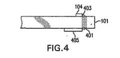
本発明によるPCBとして使用されるフェライト基板によって、他の回路構成要素に対する高周波ノイズの有害な影響は、例えば、“通路”のようなフェライト基板中で駆動リード線を経路付けすることによって実質的に緩和されても良い。図4に示されているように、本発明のこの特徴に従って、通路401がフェライト基板101内に形成されている。LED104は基板101の一方の側に取り付けられており、駆動回路405は基板101の他方の側に取り付けることができる。駆動回路405からの駆動信号導電体403は、通路401によってLED104へと経路を定められ、このようにして、LED駆動に対する高周波ノイズの影響を減らす。ノイズを濾波するために必要とされる1以上の通路を有するフェライト基板を構成しても良い。回路構成要素からのリード線は、ノイズを濾波するのに必要とされる1以上の通路によって経路を定められても良い。この1以上の回路構成要素からのリード線は、同じ通路又は異なる通路によって経路を定められても良い。 With the ferrite substrate used as a PCB according to the present invention, the detrimental effect of high frequency noise on other circuit components is substantially reduced by routing the drive leads in a ferrite substrate, such as a “passage”. It may be relaxed. As shown in FIG. 4, in accordance with this aspect of the invention, a
更に、人間(又はあらゆる他の動物)の体内に配置されている如何なる埋め込み部材、“生体適合性”材料によって作られている埋め込み部材でさえ、ある場合には、埋め込み部材が刺激を与えるという事実によって埋め込み部材が挿入される生物体内に“異物反応”を生じさせることは理解できるであろう。人体内に埋め込まれるセンサー10の場合には、“異物反応”は、繊維状カプセル封入すなわち瘢痕組織の形成であることが最も多い。グルコース(本発明によるセンサーが検知するために使用されると期待されている主要な分析物)は、このような繊維状カプセル封入によって妨害される拡散又は移動の速度を有するかも知れない。これは単に、繊維状カプセル封入を形成している細胞(瘢痕組織)が全く稠密な性質であるか又は通常の組織とは異なる代謝特性を有し得るからである。 Furthermore, any implant placed in the body of a human (or any other animal), even an implant made of a “biocompatible” material, in some cases, the fact that the implant gives a stimulus It will be understood that this causes a “foreign body reaction” in the organism into which the implant is inserted. In the case of the
この潜在的な妨害に打ち勝つか又は生物学的分析物に対する指示分子の曝露を遅らせるためには、2つの主要な方法が考えられる。おそらく最も簡単な方法である1つの方法に従って、センサー/組織境界層(指示分子がセンサー本体の表面上に直接固定されているときにセンサー本体12及び/又は指示分子自体の表面を覆っているか又は指示分子がその中に含まれているときに基質層14の表面を覆っている)が、繊維状カプセル封入の低い又は許容できるレベルが形成されるようにさせる材料によって作られる。この特性を有するものとして文献内に記載されているこのような材料の2つの例は、W.I.Goreから入手可能なPreclude(登録商標)Periocardial Membrane及びケネディによる“Tailoring Polymers for Biological Vses”(1994年2月号のChemtech第24乃至31頁)に記載されている親水性の共有結合されたポリブチレンである。 Two major approaches are conceivable to overcome this potential interference or delay the exposure of the indicator molecule to the biological analyte. According to one method, perhaps the simplest method, the sensor / tissue boundary layer (which covers the surface of the
別の方法として、特別化された生体適合性材料の幾つかの層によって構成されているセンサー/組織境界層をセンサーを覆うようにして設けることができる。図8に示されているように、例えば、このセンサー/組織境界層36は、3つの副層36a,36b,36cを含んでいても良い。組織の内殖を促進する層である副層36aは、繊維状細胞39(瘢痕組織)がその上に蓄積するときでさえ、毛細管37の貫入を許容する生体適合性材料によって作られている。ゴアテックス(登録商標)脈管移植片材料(ePTFE)、長年に亘って使用されて来たDacron(登録商標)(PET)脈管移植片材料及び(POREX Surgical Inc.,から入手可能である)高密度ポリエチレンによって作られたMEDROR生体適合材料は、その基本組成、ポアサイズ及びポア構造が組織内殖層内への組織及び脈管の内殖を促進する材料の例である。 Alternatively, a sensor / tissue boundary layer composed of several layers of specialized biocompatible material can be provided over the sensor. As shown in FIG. 8, for example, the sensor /
他方、副層36bは、組織の内殖を防止するために、組織内殖副層36aのポアサイズよりも著しく小さいポアサイズ(5マイクロメートル未満)を備えた生体適合性の層であるのが好ましい。副層36bが作られるべき現在の好ましい材料は、拡張テトラ−フルオロエチレン(ePTFE)からなるW.L.Gore,Inc.,から入手可能であるPreclude Perocardial Membrane(以前はGORE−TEX Surgical Membrane(ゴアテックス外科用膜)と呼ばれていた)である。 On the other hand, sublayer 36b is preferably a biocompatible layer with a pore size (less than 5 micrometers) significantly smaller than the pore size of tissue ingrowth sublayer 36a to prevent tissue ingrowth. A presently preferred material from which sublayer 36b is to be made is a W.M. made of expanded tetra-fluoroethylene (ePTFE). L. Gore, Inc. , Prelude Perocardial Membrane (formerly called GORE-TEX Surgical Membrane).
第3の副層36cは分子篩いとして機能する。すなわた、これは、問題となっている分析物が貫通して指示分子(センサー本体12上に直にコーティングされているか又は基質層14内に固定されている)へと届くのを許容しつつ、免疫グロブリン、プロテイン及びグリコプロテインのような分子を排除する分子量カットオフ機能を提供する。多くの公知のセルロースタイプの膜、例えば、腎臓透析濾過カートリッジリッドにおいて使用される種類のセルロースタイプの膜が、分子量カットオフ層36cのために使用されても良い。 The
以下に認められるように、図6に示されたセンサーは、全体として自蔵されていて、電気リード線が、センサーに(例えば、センサー18を駆動するための)電力を供給するためか又はセンサーからの信号を送るためにセンサー本体内へ又はセンサー本体から延びるようになされている。図2に示された電子部品の全てが図6に示されているようにモジュール66内に収容されている。 As will be appreciated, the sensor shown in FIG. 6 is self-contained as a whole and the electrical leads provide power to the sensor (eg, to drive the sensor 18) or the sensor Extending into or from the sensor body to send signals from the sensor body. All of the electronic components shown in FIG. 2 are housed in a
同じく、以下において認識されるように、図6乃至8に記載された蛍光に基づくセンサーの実施形態は、ちょうど本発明を適用することができる例である。本発明はまた、例えば、本明細書に参考として組み入れられている1999年8月28日に出願された米国特許第第69/383,148号に記載されている吸収に基づくセンサー又は屈折率に基づくセンサーのような多数の他の用途に適用されても良い。 Similarly, as will be recognized below, the fluorescence-based sensor embodiments described in FIGS. 6-8 are just examples to which the present invention can be applied. The present invention also includes an absorption based sensor or refractive index as described, for example, in US Pat. No. 69 / 383,148, filed Aug. 28, 1999, which is incorporated herein by reference. It may be applied to many other applications, such as based sensors.
以上、本発明を説明したが、本発明の精神及び範囲を逸脱することなく多くの方法で本発明を変更しても良いことは当業者にとって明らかとなるであろう。例えば、本発明を埋め込まれたセンサー装置を参考にして説明したが、本発明の原理は、回路基板上データ又は信号電力伝送機能を使用した無線伝送機能を有するあらゆるプリント回路基板に適用しても良い。このような変形例のあらゆる且つ全てのものが特許請求の範囲に包含されることを意図している。 While the invention has been described above, it will be apparent to those skilled in the art that the invention may be modified in many ways without departing from the spirit and scope of the invention. For example, although the present invention has been described with reference to an embedded sensor device, the principles of the present invention may be applied to any printed circuit board having a wireless transmission function using data on a circuit board or a signal power transmission function. good. All and all such variations are intended to be included within the scope of the claims.
Claims (25)
Translated fromJapanese実質的にフェライト材料によって形成された基板であって、頂面及び底面と、当該基板の大きい方の寸法に沿って前記頂面と底面との間に延びている第一及び第二の側面と、当該基板の小さい方の寸法に沿って前記頂面と底面との間に延びている第一及び第二の端面とを備えた前記基板と、
前記基板の主面に取り付けられた少なくとも1つの回路構成要素と、
前記基板上に形成され且つ前記主面及び側面のうちの一方の上にコイル状に延びている導電部材とを含むプリント回路装置。A printed circuit device,
A substrate substantially formed of a ferrite material, the top and bottom surfaces, and first and second side surfaces extending between the top and bottom surfaces along the larger dimension of the substrate; The substrate with first and second end surfaces extending between the top and bottom surfaces along the smaller dimension of the substrate;
At least one circuit component attached to a major surface of the substrate;
A printed circuit device comprising: a conductive member formed on the substrate and extending in a coil shape on one of the main surface and the side surface.
前記少なくとも1つの回路構成要素であるリード線が、前記基板に形成された通路によって経路を定められているプリント回路装置。The printed circuit device according to claim 1,
A printed circuit device in which a lead wire as the at least one circuit component is routed by a passage formed in the substrate.
前記少なくとも1つの回路構成要素が、発光ダイオード(LED)及び当該LEDのためのリード線を含んでいるプリント回路装置。The printed circuit device according to claim 2,
A printed circuit device wherein the at least one circuit component includes a light emitting diode (LED) and a lead for the LED.
前記LEDのための前記リード線が駆動リード線であるプリント回路装置。The printed circuit device according to claim 3,
A printed circuit device wherein the lead for the LED is a drive lead.
前記少なくとも1つの回路構成要素のリード線が、前記基板内に形成された複数の通路によって経路が定められているプリント回路装置。The printed circuit device according to claim 2,
A printed circuit device in which a lead wire of the at least one circuit component is routed by a plurality of passages formed in the substrate.
前記複数の回路構成要素のリード線が、前記基板内に形成された複数の通路によって経路が定められているプリント回路装置。The printed circuit device according to claim 5,
A printed circuit device in which the leads of the plurality of circuit components are routed by a plurality of passages formed in the substrate.
前記コイルが、前記基板に近接してへり結合によって結合されているプリント回路装置。The printed circuit device according to claim 1,
A printed circuit device in which the coil is coupled by edge coupling in proximity to the substrate.
前記コイルが、外部装置に対してデータ信号を伝送するために使用されているプリント回路装置。The printed circuit device according to claim 1,
A printed circuit device in which the coil is used to transmit a data signal to an external device.
前記コイルが、外部電源からの電力の誘導伝送のために使用されているプリント回路装置。The printed circuit device according to claim 1,
A printed circuit device in which the coil is used for inductive transmission of power from an external power source.
当該プリント回路装置が、生物の体内の定量分析物測定を行う埋め込みセンサー装置の構成要素であるプリント回路装置。The printed circuit device according to claim 1,
A printed circuit device, wherein the printed circuit device is a component of an embedded sensor device that measures a quantitative analyte in a living organism.
前記少なくとも1つの回路構成要素が発光ダイオード(LED)を含み、前記プリント回路装置が少なくとも1つの光検知器を更に含んでいるプリント回路装置。The printed circuit device according to claim 10, comprising:
The printed circuit device, wherein the at least one circuit component includes a light emitting diode (LED), and the printed circuit device further includes at least one photodetector.
実質的にフェライト材料からなるプリント回路装置を形成すること、及び
前記プリント回路装置を前記誘導コイルのためのフェライトコアとして使用することを特徴とする電子装置。An electronic device comprising an integrated circuit formed on a printed circuit device and an induction coil for data and / or power transmission,
An electronic device comprising: forming a printed circuit device substantially made of a ferrite material; and using the printed circuit device as a ferrite core for the induction coil.
媒体と相互作用する蛍光指示器内に光を導入するための光源と、
前記導入された光に応答して前記蛍光指示器によって発せられる光を検知し且つ検知した光に比例する信号を出力するための光検知器であって、前記蛍光指示器の応答は、前記媒体内の分析物の存在及び量に応じて変化するようになされた光検知器と、
外部電源からの電力を受け取り且つ外部処理装置に前記信号を送るためのコイルと、
実質的にフェライト材料によって形成された基板であって、前記光源及び前記光検知器が当該基板上に取り付けられ、前記コイルが、前記フェライト材料が前記コイルの誘導特性を増すように当該基板上に形成されている前記基板とを含む蛍光センサー装置。A fluorescence sensor device,
A light source for introducing light into the fluorescent indicator interacting with the medium;
A light detector for detecting light emitted by the fluorescent indicator in response to the introduced light and outputting a signal proportional to the detected light, wherein the response of the fluorescent indicator is the medium A light detector adapted to vary depending on the presence and amount of the analyte within,
A coil for receiving power from an external power source and sending the signal to an external processing device;
A substrate substantially formed of a ferrite material, wherein the light source and the photodetector are mounted on the substrate, and the coil is disposed on the substrate such that the ferrite material increases the inductive characteristics of the coil. A fluorescent sensor device comprising the substrate being formed.
前記光源及び前記光検知器が前記基板の第一の部分に取り付けられており、前記コイルが前記基板の第二の部分に形成されている蛍光センサー装置。The fluorescence sensor device according to claim 13,
The fluorescence sensor device, wherein the light source and the light detector are attached to a first portion of the substrate, and the coil is formed on a second portion of the substrate.
前記コイルが前記基板の反対側の面に近接して延びている蛍光センサー装置。The fluorescence sensor device according to claim 13,
A fluorescent sensor device in which the coil extends close to an opposite surface of the substrate.
前記光源が、前記基板に形成された通路によって経路が定められている蛍光センサー装置。The fluorescence sensor device according to claim 13,
A fluorescent sensor device in which the light source is routed by a passage formed in the substrate.
前記コイルが前記基板に近接してへり巻き付けによって巻き付けられている蛍光センサー装置。The fluorescence sensor device according to claim 13,
A fluorescent sensor device in which the coil is wound by edge winding close to the substrate.
前記コイルが、外部装置へのデータ信号の伝送のために使用されている蛍光センサー装置。The fluorescence sensor device according to claim 13,
A fluorescence sensor device in which the coil is used to transmit a data signal to an external device.
前記コイルが、外部電源からの電力の誘導による受け取りのために使用されている蛍光センサー装置。The fluorescence sensor device according to claim 13,
A fluorescent sensor device in which the coil is used for receiving by induction of power from an external power source.
生物の体の内部の分析物定量測定を行う埋め込み可能なセンサー装置を含んでいる蛍光センサー装置。The fluorescence sensor device according to claim 13,
A fluorescent sensor device that includes an implantable sensor device that performs an analyte quantitative measurement within the body of a living organism.
生物の体の内部の分析物定性測定を行う埋め込み可能なセンサー装置を含んでいる蛍光センサー装置。The fluorescence sensor device according to claim 13,
A fluorescence sensor device that includes an implantable sensor device that performs an analyte qualitative measurement within the body of a living organism.
前記光源が発光ダイオード(LED)を含み、前記基板が少なくとも一つの光検知器を更に含んでいる蛍光センサー装置。The fluorescence sensor device according to claim 20,
The fluorescent sensor device, wherein the light source includes a light emitting diode (LED) and the substrate further includes at least one photodetector.
回路構成要素のための導電部材の経路を定めるために、前記基板内に形成された通路を更に含んでいる蛍光センサー装置。The fluorescence sensor device according to claim 13,
A fluorescent sensor device further comprising a passage formed in the substrate for defining a path of a conductive member for a circuit component.
回路構成要素のための導電部材の経路を定めるために、前記基板内に形成された通路を更に含んでいるプリント回路装置。The printed circuit device according to claim 1,
A printed circuit device further comprising a passage formed in the substrate for defining a path of a conductive member for a circuit component.
媒体と相互作用する蛍光指示器内に光を導入するための光源と、
前記導入された光に応答して前記蛍光指示器によって発せられる光を検知し且つ検知した光に比例する信号を出力するための光検知器であって、前記蛍光指示器の応答は、前記媒体内の分析物の存在及び量に応じて変化するようになされた光検知器と、
前記光源及び前記光検知器が取り付けられている基板とを含み、
光学フィルタが、前記光検知器上に直に配置されている蛍光センサー装置。A fluorescence sensor device,
A light source for introducing light into the fluorescent indicator interacting with the medium;
A light detector for detecting light emitted by the fluorescent indicator in response to the introduced light and outputting a signal proportional to the detected light, wherein the response of the fluorescent indicator is the medium A light detector adapted to vary depending on the presence and amount of the analyte within,
A substrate on which the light source and the light detector are attached,
A fluorescence sensor device in which an optical filter is arranged directly on the photodetector.
Applications Claiming Priority (2)
| Application Number | Priority Date | Filing Date | Title |
|---|---|---|---|
| US46269503P | 2003-04-15 | 2003-04-15 | |
| PCT/US2004/011393WO2004093504A2 (en) | 2003-04-15 | 2004-04-14 | Printed circuit device with integrated antenna and implantable sensor processing system with integrated printed circuit board antenna |
Related Child Applications (1)
| Application Number | Title | Priority Date | Filing Date |
|---|---|---|---|
| JP2010210810ADivisionJP2011004427A (en) | 2003-04-15 | 2010-09-21 | Printed circuit device with integrated antenna and implantable sensor processing device with integrated printed circuit board antenna |
Publications (1)
| Publication Number | Publication Date |
|---|---|
| JP2007525858Atrue JP2007525858A (en) | 2007-09-06 |
Family
ID=33299973
Family Applications (5)
| Application Number | Title | Priority Date | Filing Date |
|---|---|---|---|
| JP2006509990APendingJP2007525858A (en) | 2003-04-15 | 2004-04-14 | Printed circuit device with integrated antenna and implantable sensor processing device with printed integrated circuit board antenna |
| JP2006509989APendingJP2006523843A (en) | 2003-04-15 | 2004-04-14 | Apparatus and method for reducing the effect of ambient light on an optical sensor |
| JP2010140820AExpired - LifetimeJP5415364B2 (en) | 2003-04-15 | 2010-06-21 | Sensor designed to reduce the influence of ambient light on the sensor |
| JP2010210810APendingJP2011004427A (en) | 2003-04-15 | 2010-09-21 | Printed circuit device with integrated antenna and implantable sensor processing device with integrated printed circuit board antenna |
| JP2013085393AExpired - Fee RelatedJP5603968B2 (en) | 2003-04-15 | 2013-04-16 | Apparatus and method for reducing the effect of ambient light on an optical sensor |
Family Applications After (4)
| Application Number | Title | Priority Date | Filing Date |
|---|---|---|---|
| JP2006509989APendingJP2006523843A (en) | 2003-04-15 | 2004-04-14 | Apparatus and method for reducing the effect of ambient light on an optical sensor |
| JP2010140820AExpired - LifetimeJP5415364B2 (en) | 2003-04-15 | 2010-06-21 | Sensor designed to reduce the influence of ambient light on the sensor |
| JP2010210810APendingJP2011004427A (en) | 2003-04-15 | 2010-09-21 | Printed circuit device with integrated antenna and implantable sensor processing device with integrated printed circuit board antenna |
| JP2013085393AExpired - Fee RelatedJP5603968B2 (en) | 2003-04-15 | 2013-04-16 | Apparatus and method for reducing the effect of ambient light on an optical sensor |
Country Status (13)
| Country | Link |
|---|---|
| US (5) | US7157723B2 (en) |
| EP (2) | EP1618768B1 (en) |
| JP (5) | JP2007525858A (en) |
| KR (5) | KR20060004942A (en) |
| CN (6) | CN104034707B (en) |
| AU (2) | AU2004230528B2 (en) |
| BR (3) | BRPI0409435A (en) |
| CA (3) | CA2522281C (en) |
| DK (2) | DK1620714T3 (en) |
| MX (2) | MXPA05011165A (en) |
| SG (3) | SG182002A1 (en) |
| TW (2) | TWI369927B (en) |
| WO (2) | WO2004093504A2 (en) |
Cited By (8)
| Publication number | Priority date | Publication date | Assignee | Title |
|---|---|---|---|---|
| US9041582B2 (en) | 2010-07-16 | 2015-05-26 | Olympus Corporation | Organism state quantity measuring apparatus |
| JP2018521823A (en)* | 2015-07-24 | 2018-08-09 | ゼヴェクス・インコーポレーテッド | Magnetic pressure sensing system for infusion pumps |
| US10952621B2 (en) | 2017-12-05 | 2021-03-23 | Cardiac Pacemakers, Inc. | Multimodal analyte sensor optoelectronic interface |
| US11089983B2 (en) | 2017-12-01 | 2021-08-17 | Cardiac Pacemakers, Inc. | Multimodal analyte sensors for medical devices |
| US11129557B2 (en) | 2017-05-31 | 2021-09-28 | Cardiac Pacemakers, Inc. | Implantable medical device with chemical sensor |
| US11439304B2 (en) | 2017-08-10 | 2022-09-13 | Cardiac Pacemakers, Inc. | Systems and methods including electrolyte sensor fusion |
| US11571151B2 (en) | 2017-08-23 | 2023-02-07 | Cardiac Pacemakers, Inc. | Implantable chemical sensor with staged activation |
| US12004853B2 (en) | 2017-07-26 | 2024-06-11 | Cardiac Pacemakers, Inc. | Systems and methods for disambiguation of posture |
Families Citing this family (180)
| Publication number | Priority date | Publication date | Assignee | Title |
|---|---|---|---|---|
| US6391005B1 (en)* | 1998-03-30 | 2002-05-21 | Agilent Technologies, Inc. | Apparatus and method for penetration with shaft having a sensor for sensing penetration depth |
| US8641644B2 (en) | 2000-11-21 | 2014-02-04 | Sanofi-Aventis Deutschland Gmbh | Blood testing apparatus having a rotatable cartridge with multiple lancing elements and testing means |
| US7344507B2 (en) | 2002-04-19 | 2008-03-18 | Pelikan Technologies, Inc. | Method and apparatus for lancet actuation |
| US8337419B2 (en)* | 2002-04-19 | 2012-12-25 | Sanofi-Aventis Deutschland Gmbh | Tissue penetration device |
| US9427532B2 (en) | 2001-06-12 | 2016-08-30 | Sanofi-Aventis Deutschland Gmbh | Tissue penetration device |
| US9226699B2 (en) | 2002-04-19 | 2016-01-05 | Sanofi-Aventis Deutschland Gmbh | Body fluid sampling module with a continuous compression tissue interface surface |
| US7749174B2 (en) | 2001-06-12 | 2010-07-06 | Pelikan Technologies, Inc. | Method and apparatus for lancet launching device intergrated onto a blood-sampling cartridge |
| US7981056B2 (en) | 2002-04-19 | 2011-07-19 | Pelikan Technologies, Inc. | Methods and apparatus for lancet actuation |
| US9795747B2 (en) | 2010-06-02 | 2017-10-24 | Sanofi-Aventis Deutschland Gmbh | Methods and apparatus for lancet actuation |
| US7041068B2 (en)* | 2001-06-12 | 2006-05-09 | Pelikan Technologies, Inc. | Sampling module device and method |
| JP4209767B2 (en)* | 2001-06-12 | 2009-01-14 | ペリカン テクノロジーズ インコーポレイテッド | Self-optimized cutting instrument with adaptive means for temporary changes in skin properties |
| EP1395185B1 (en) | 2001-06-12 | 2010-10-27 | Pelikan Technologies Inc. | Electric lancet actuator |
| US7229458B2 (en) | 2002-04-19 | 2007-06-12 | Pelikan Technologies, Inc. | Method and apparatus for penetrating tissue |
| US7297122B2 (en)* | 2002-04-19 | 2007-11-20 | Pelikan Technologies, Inc. | Method and apparatus for penetrating tissue |
| US8360992B2 (en) | 2002-04-19 | 2013-01-29 | Sanofi-Aventis Deutschland Gmbh | Method and apparatus for penetrating tissue |
| US8267870B2 (en) | 2002-04-19 | 2012-09-18 | Sanofi-Aventis Deutschland Gmbh | Method and apparatus for body fluid sampling with hybrid actuation |
| US7232451B2 (en) | 2002-04-19 | 2007-06-19 | Pelikan Technologies, Inc. | Method and apparatus for penetrating tissue |
| US7708701B2 (en) | 2002-04-19 | 2010-05-04 | Pelikan Technologies, Inc. | Method and apparatus for a multi-use body fluid sampling device |
| US7909778B2 (en) | 2002-04-19 | 2011-03-22 | Pelikan Technologies, Inc. | Method and apparatus for penetrating tissue |
| US7901362B2 (en)* | 2002-04-19 | 2011-03-08 | Pelikan Technologies, Inc. | Method and apparatus for penetrating tissue |
| US7976476B2 (en) | 2002-04-19 | 2011-07-12 | Pelikan Technologies, Inc. | Device and method for variable speed lancet |
| US7547287B2 (en) | 2002-04-19 | 2009-06-16 | Pelikan Technologies, Inc. | Method and apparatus for penetrating tissue |
| US8784335B2 (en) | 2002-04-19 | 2014-07-22 | Sanofi-Aventis Deutschland Gmbh | Body fluid sampling device with a capacitive sensor |
| US9248267B2 (en) | 2002-04-19 | 2016-02-02 | Sanofi-Aventis Deustchland Gmbh | Tissue penetration device |
| US7674232B2 (en) | 2002-04-19 | 2010-03-09 | Pelikan Technologies, Inc. | Method and apparatus for penetrating tissue |
| US8221334B2 (en) | 2002-04-19 | 2012-07-17 | Sanofi-Aventis Deutschland Gmbh | Method and apparatus for penetrating tissue |
| US9795334B2 (en) | 2002-04-19 | 2017-10-24 | Sanofi-Aventis Deutschland Gmbh | Method and apparatus for penetrating tissue |
| US7331931B2 (en) | 2002-04-19 | 2008-02-19 | Pelikan Technologies, Inc. | Method and apparatus for penetrating tissue |
| US8579831B2 (en) | 2002-04-19 | 2013-11-12 | Sanofi-Aventis Deutschland Gmbh | Method and apparatus for penetrating tissue |
| US7892183B2 (en) | 2002-04-19 | 2011-02-22 | Pelikan Technologies, Inc. | Method and apparatus for body fluid sampling and analyte sensing |
| US9314194B2 (en)* | 2002-04-19 | 2016-04-19 | Sanofi-Aventis Deutschland Gmbh | Tissue penetration device |
| US8372016B2 (en)* | 2002-04-19 | 2013-02-12 | Sanofi-Aventis Deutschland Gmbh | Method and apparatus for body fluid sampling and analyte sensing |
| US7648468B2 (en)* | 2002-04-19 | 2010-01-19 | Pelikon Technologies, Inc. | Method and apparatus for penetrating tissue |
| US8702624B2 (en) | 2006-09-29 | 2014-04-22 | Sanofi-Aventis Deutschland Gmbh | Analyte measurement device with a single shot actuator |
| US7491178B2 (en) | 2002-04-19 | 2009-02-17 | Pelikan Technologies, Inc. | Method and apparatus for penetrating tissue |
| US20040106163A1 (en)* | 2002-11-12 | 2004-06-03 | Workman Jerome James | Non-invasive measurement of analytes |
| AU2003287735A1 (en) | 2002-11-12 | 2004-06-03 | Argose, Inc. | Non-invasive measurement of analytes |
| US8574895B2 (en) | 2002-12-30 | 2013-11-05 | Sanofi-Aventis Deutschland Gmbh | Method and apparatus using optical techniques to measure analyte levels |
| US7811231B2 (en) | 2002-12-31 | 2010-10-12 | Abbott Diabetes Care Inc. | Continuous glucose monitoring system and methods of use |
| JP2007525858A (en)* | 2003-04-15 | 2007-09-06 | センサーズ・フォー・メデセン・アンド・サイエンス・インコーポレーテッド | Printed circuit device with integrated antenna and implantable sensor processing device with printed integrated circuit board antenna |
| WO2004103147A2 (en)* | 2003-05-02 | 2004-12-02 | Pelikan Technologies, Inc. | Method and apparatus for a tissue penetrating device user interface |
| DE602004028463D1 (en) | 2003-05-30 | 2010-09-16 | Pelikan Technologies Inc | METHOD AND DEVICE FOR INJECTING LIQUID |
| US7850621B2 (en) | 2003-06-06 | 2010-12-14 | Pelikan Technologies, Inc. | Method and apparatus for body fluid sampling and analyte sensing |
| US8066639B2 (en) | 2003-06-10 | 2011-11-29 | Abbott Diabetes Care Inc. | Glucose measuring device for use in personal area network |
| WO2006001797A1 (en) | 2004-06-14 | 2006-01-05 | Pelikan Technologies, Inc. | Low pain penetrating |
| US7920906B2 (en) | 2005-03-10 | 2011-04-05 | Dexcom, Inc. | System and methods for processing analyte sensor data for sensor calibration |
| US8282576B2 (en) | 2003-09-29 | 2012-10-09 | Sanofi-Aventis Deutschland Gmbh | Method and apparatus for an improved sample capture device |
| EP1680014A4 (en) | 2003-10-14 | 2009-01-21 | Pelikan Technologies Inc | METHOD AND DEVICE FOR A VARIABLE USER INTERFACE |
| WO2005065241A2 (en)* | 2003-12-24 | 2005-07-21 | Argose, Inc. | Smmr (small molecule metabolite reporters) for use as in vivo glucose biosensors |
| US8668656B2 (en) | 2003-12-31 | 2014-03-11 | Sanofi-Aventis Deutschland Gmbh | Method and apparatus for improving fluidic flow and sample capture |
| US7822454B1 (en) | 2005-01-03 | 2010-10-26 | Pelikan Technologies, Inc. | Fluid sampling device with improved analyte detecting member configuration |
| WO2005089103A2 (en) | 2004-02-17 | 2005-09-29 | Therasense, Inc. | Method and system for providing data communication in continuous glucose monitoring and management system |
| US20050234316A1 (en) | 2004-04-16 | 2005-10-20 | Sensors For Medicine And Science, Inc. | Housing for a circuit that is to be implanted in-vivo and process of making the same |
| US7375347B2 (en)* | 2004-04-26 | 2008-05-20 | Sensors For Medicine And Science, Inc. | Systems and methods for extending the useful life of optical sensors |
| WO2006011062A2 (en) | 2004-05-20 | 2006-02-02 | Albatros Technologies Gmbh & Co. Kg | Printable hydrogel for biosensors |
| WO2005120365A1 (en) | 2004-06-03 | 2005-12-22 | Pelikan Technologies, Inc. | Method and apparatus for a fluid sampling device |
| US9775553B2 (en) | 2004-06-03 | 2017-10-03 | Sanofi-Aventis Deutschland Gmbh | Method and apparatus for a fluid sampling device |
| US7334067B2 (en)* | 2004-06-03 | 2008-02-19 | Sp Controls, Inc. | Programmable controller having reduced control key set |
| US7654956B2 (en) | 2004-07-13 | 2010-02-02 | Dexcom, Inc. | Transcutaneous analyte sensor |
| US9788771B2 (en) | 2006-10-23 | 2017-10-17 | Abbott Diabetes Care Inc. | Variable speed sensor insertion devices and methods of use |
| US8652831B2 (en) | 2004-12-30 | 2014-02-18 | Sanofi-Aventis Deutschland Gmbh | Method and apparatus for analyte measurement test time |
| US20060167382A1 (en)* | 2004-12-30 | 2006-07-27 | Ajay Deshmukh | Method and apparatus for storing an analyte sampling and measurement device |
| US20090030293A1 (en)* | 2005-02-11 | 2009-01-29 | The University Court Of The University Of Glasgow | Sensing device, apparatus and system, and method for operating the same |
| US7308292B2 (en)* | 2005-04-15 | 2007-12-11 | Sensors For Medicine And Science, Inc. | Optical-based sensing devices |
| US7233711B1 (en)* | 2005-05-11 | 2007-06-19 | Hewlett Packard Development Company, L.P. | Autonomous evanescent optical nanosensor |
| EP1886126A4 (en)* | 2005-06-02 | 2010-07-28 | Glaxo Group Ltd | Inductively powered remote oxygen sensor |
| US20070194247A1 (en)* | 2005-08-31 | 2007-08-23 | Stratagene California | Compact optical module for fluorescence excitation and detection |
| US7705313B1 (en)* | 2005-10-18 | 2010-04-27 | Ric Investments, Llc | Ambient gas compensation in an optical system |
| US7766829B2 (en) | 2005-11-04 | 2010-08-03 | Abbott Diabetes Care Inc. | Method and system for providing basal profile modification in analyte monitoring and management systems |
| EP2014224A1 (en)* | 2006-03-24 | 2009-01-14 | GlucoTel Scientific Inc. | Telemedical method and device for the calibration of measured values |
| US7620438B2 (en) | 2006-03-31 | 2009-11-17 | Abbott Diabetes Care Inc. | Method and system for powering an electronic device |
| US8226891B2 (en) | 2006-03-31 | 2012-07-24 | Abbott Diabetes Care Inc. | Analyte monitoring devices and methods therefor |
| US7515822B2 (en)* | 2006-05-12 | 2009-04-07 | Microsoft Corporation | Imaging systems' direct illumination level adjusting method and system involves adjusting operation of image sensor of imaging system based on detected level of ambient illumination |
| US7809441B2 (en) | 2006-05-17 | 2010-10-05 | Cardiac Pacemakers, Inc. | Implantable medical device with chemical sensor and related methods |
| TWI302043B (en)* | 2006-06-27 | 2008-10-11 | Everlight Electronics Co Ltd | Base structure for ultra-thin light-emitting diode and manufacturing method thereof |
| CN101169340B (en)* | 2006-10-27 | 2010-12-08 | 鸿富锦精密工业(深圳)有限公司 | Motherboard light-emitting diode detection device and method |
| US20080199894A1 (en) | 2007-02-15 | 2008-08-21 | Abbott Diabetes Care, Inc. | Device and method for automatic data acquisition and/or detection |
| JP4488011B2 (en)* | 2007-02-26 | 2010-06-23 | エプソンイメージングデバイス株式会社 | Electro-optical device, semiconductor device, display device, and electronic apparatus including the same |
| US8123686B2 (en) | 2007-03-01 | 2012-02-28 | Abbott Diabetes Care Inc. | Method and apparatus for providing rolling data in communication systems |
| WO2008130895A2 (en) | 2007-04-14 | 2008-10-30 | Abbott Diabetes Care, Inc. | Method and apparatus for providing dynamic multi-stage signal amplification in a medical device |
| US7928850B2 (en) | 2007-05-08 | 2011-04-19 | Abbott Diabetes Care Inc. | Analyte monitoring system and methods |
| US8456301B2 (en) | 2007-05-08 | 2013-06-04 | Abbott Diabetes Care Inc. | Analyte monitoring system and methods |
| US8665091B2 (en) | 2007-05-08 | 2014-03-04 | Abbott Diabetes Care Inc. | Method and device for determining elapsed sensor life |
| US8461985B2 (en) | 2007-05-08 | 2013-06-11 | Abbott Diabetes Care Inc. | Analyte monitoring system and methods |
| WO2008157820A1 (en) | 2007-06-21 | 2008-12-24 | Abbott Diabetes Care, Inc. | Health management devices and methods |
| US7805174B2 (en) | 2007-09-18 | 2010-09-28 | Cardiac Pacemakers, Inc. | Implantable electro-optical sensor |
| US20090247984A1 (en)* | 2007-10-24 | 2009-10-01 | Masimo Laboratories, Inc. | Use of microneedles for small molecule metabolite reporter delivery |
| US7907061B2 (en)* | 2007-11-14 | 2011-03-15 | Intersil Americas Inc. | Proximity sensors and methods for sensing proximity |
| US8290557B2 (en)* | 2007-12-12 | 2012-10-16 | Medtronic, Inc. | Implantable optical sensor and method for use |
| US20090159801A1 (en)* | 2007-12-21 | 2009-06-25 | Newport Corporation | Fluorescence optical coatings and methods for producing same |
| US20090209883A1 (en)* | 2008-01-17 | 2009-08-20 | Michael Higgins | Tissue penetrating apparatus |
| EP2982383B1 (en) | 2008-04-10 | 2019-05-15 | Abbott Diabetes Care, Inc. | Method for sterilizing an analyte sensor |
| EP2265324B1 (en)* | 2008-04-11 | 2015-01-28 | Sanofi-Aventis Deutschland GmbH | Integrated analyte measurement system |
| US20090294277A1 (en)* | 2008-05-30 | 2009-12-03 | Abbott Diabetes Care, Inc. | Method and system for producing thin film biosensors |
| US20100004518A1 (en) | 2008-07-03 | 2010-01-07 | Masimo Laboratories, Inc. | Heat sink for noninvasive medical sensor |
| US8515509B2 (en) | 2008-08-04 | 2013-08-20 | Cercacor Laboratories, Inc. | Multi-stream emitter for noninvasive measurement of blood constituents |
| US9375169B2 (en) | 2009-01-30 | 2016-06-28 | Sanofi-Aventis Deutschland Gmbh | Cam drive for managing disposable penetrating member actions with a single motor and motor and control system |
| US9402544B2 (en) | 2009-02-03 | 2016-08-02 | Abbott Diabetes Care Inc. | Analyte sensor and apparatus for insertion of the sensor |
| US8921280B2 (en) | 2009-02-11 | 2014-12-30 | Samsung Electronics Co., Ltd. | Integrated bio-chip and method of fabricating the integrated bio-chip |
| US7935935B2 (en)* | 2009-02-27 | 2011-05-03 | Medtronic, Inc. | Radiation-based timer for implantable medical devices |
| WO2010127050A1 (en) | 2009-04-28 | 2010-11-04 | Abbott Diabetes Care Inc. | Error detection in critical repeating data in a wireless sensor system |
| WO2010138856A1 (en) | 2009-05-29 | 2010-12-02 | Abbott Diabetes Care Inc. | Medical device antenna systems having external antenna configurations |
| US8993331B2 (en) | 2009-08-31 | 2015-03-31 | Abbott Diabetes Care Inc. | Analyte monitoring system and methods for managing power and noise |
| EP3001194B1 (en) | 2009-08-31 | 2019-04-17 | Abbott Diabetes Care, Inc. | Medical devices and methods |
| US9314195B2 (en) | 2009-08-31 | 2016-04-19 | Abbott Diabetes Care Inc. | Analyte signal processing device and methods |
| US9357957B2 (en) | 2010-01-21 | 2016-06-07 | Arkray, Inc. | Measuring apparatus, measuring system, electric power supply apparatus, and electric power supply method |
| JP5663900B2 (en) | 2010-03-05 | 2015-02-04 | セイコーエプソン株式会社 | Spectroscopic sensor device and electronic device |
| WO2011111008A1 (en) | 2010-03-11 | 2011-09-15 | Ecole Polytechnique Federale De Lausanne (Epfl) | Telemetry system for sensing applications in lossy media |
| US8965476B2 (en) | 2010-04-16 | 2015-02-24 | Sanofi-Aventis Deutschland Gmbh | Tissue penetration device |
| CN107019515B (en) | 2011-02-28 | 2021-02-26 | 雅培糖尿病护理公司 | Method of displaying sensor readings and analyte monitoring device and method of operating the same |
| US8779349B2 (en)* | 2011-03-08 | 2014-07-15 | Fluke Corporation | Minimizing ambient light in a feedback circuit in pulse oximeter test instruments |
| CN103533884B (en) | 2011-03-15 | 2016-06-01 | 传感技术股份有限公司 | The integrated catalytic protection of oxidation sensitive material |
| JP5862025B2 (en)* | 2011-03-16 | 2016-02-16 | セイコーエプソン株式会社 | Optical sensor and electronic equipment |
| CN103988238B (en) | 2011-10-11 | 2017-05-10 | 传感技术股份有限公司 | Electrodynamic field strength trigger system |
| US9069536B2 (en) | 2011-10-31 | 2015-06-30 | Abbott Diabetes Care Inc. | Electronic devices having integrated reset systems and methods thereof |
| WO2013070794A2 (en) | 2011-11-07 | 2013-05-16 | Abbott Diabetes Care Inc. | Analyte monitoring device and methods |
| US9693714B2 (en)* | 2012-02-10 | 2017-07-04 | Senseonics, Incorporated | Digital ASIC sensor platform |
| WO2013147799A1 (en) | 2012-03-29 | 2013-10-03 | Advanced Bionics Ag | Implantable antenna assemblies |
| US9377351B2 (en) | 2012-04-24 | 2016-06-28 | Senseonics, Incorporated | Angle of incidence selective band pass filter for implantable chemical sensor |
| US9968306B2 (en) | 2012-09-17 | 2018-05-15 | Abbott Diabetes Care Inc. | Methods and apparatuses for providing adverse condition notification with enhanced wireless communication range in analyte monitoring systems |
| CN103411634A (en)* | 2012-11-28 | 2013-11-27 | 上海兰宝传感科技股份有限公司 | Intelligent background suppression photoelectric sensor |
| US9006014B2 (en) | 2012-12-13 | 2015-04-14 | California Institute Of Technology | Fabrication of three-dimensional high surface area electrodes |
| US11109779B2 (en) | 2012-12-28 | 2021-09-07 | Senseonics, Incorporated | Chemical modification of analyte permeable membrane for enhanced oxidative stability |
| US9427182B2 (en) | 2012-12-28 | 2016-08-30 | Senseonics, Incorporated | Analyte permeable membrane systems for oxidative and optical stability |
| EP2953542A4 (en) | 2013-02-06 | 2016-10-05 | California Inst Of Techn | IMPLANTABLE AND MINIATURIZED ELECTROCHEMICAL SENSOR DEVICES |
| US10206624B2 (en) | 2013-03-15 | 2019-02-19 | Senseonics, Incorporated | Implantation and antenna orientation of an implantable sensor |
| CN104055492A (en)* | 2013-03-18 | 2014-09-24 | 精工爱普生株式会社 | Electronic Device |
| AU2014260023B2 (en) | 2013-04-30 | 2018-12-06 | Abbott Diabetes Care Inc. | Systems, devices, and methods for energy efficient electrical device activation |
| EP3024391B1 (en)* | 2013-07-24 | 2020-07-08 | California Institute of Technology | Design and fabrication of implantable fully integrated electrochemical sensors |
| EP3035849B1 (en) | 2013-08-21 | 2019-07-31 | Senseonics, Incorporated | Drug elution for in vivo protection of bio-sensing analytes |
| US9963556B2 (en) | 2013-09-18 | 2018-05-08 | Senseonics, Incorporated | Critical point drying of hydrogels in analyte sensors |
| CN103479363B (en)* | 2013-09-30 | 2015-03-18 | 深圳市倍轻松科技股份有限公司 | Method and system for measuring oxyhemoglobin saturation in blood |
| EP3062874B1 (en) | 2013-10-31 | 2018-02-21 | Advanced Bionics AG | Headpieces and implantable cochlear stimulation systems including the same |
| EP3068303B1 (en)* | 2013-11-15 | 2022-06-08 | Senseonics, Incorporated | Fluorescence-based sensor with multiple indicator grafts |
| US20150182967A1 (en)* | 2013-12-31 | 2015-07-02 | Canon U.S. Life Sciences, Inc. | Printed circuit board designs for laminated microfluidic devices |
| US10872048B2 (en) | 2014-01-13 | 2020-12-22 | Senseonics, Incorporated | Remotely-powered sensing system with multiple sensing devices |
| US9668698B2 (en)* | 2014-04-03 | 2017-06-06 | Koninklijke Philips N.V. | Monitoring device and method for compensating non-linearity effects in vital signs monitoring |
| ES2991768T3 (en) | 2014-07-15 | 2024-12-04 | Senseonics Inc | Integrated optical filter system with low sensitivity at high angle of incidence of light for an analyte sensor |
| WO2016014987A2 (en) | 2014-07-24 | 2016-01-28 | Thomas Jefferson University | Long-term implantable monitoring system & methods of use |
| KR20160040746A (en)* | 2014-09-26 | 2016-04-15 | 에브리봇 주식회사 | Dust sensor, dust measurement apparatus, robot cleaner and control method thereof |
| ES2923584T3 (en)* | 2015-02-24 | 2022-09-28 | Hayward Ind Inc | Pool cleaners with optical detection out of water and debris |
| JP6945451B2 (en)* | 2015-04-14 | 2021-10-06 | コーニンクレッカ フィリップス エヌ ヴェKoninklijke Philips N.V. | Intravascular devices, systems and methods with a polymer jacket formed around a communication line wrapped around a core member. |
| EP3087916B1 (en)* | 2015-04-28 | 2023-09-20 | Nokia Technologies Oy | Physiological measurement sensor |
| KR101686633B1 (en)* | 2015-05-18 | 2016-12-14 | 주식회사 아이티엠반도체 | Antenna module package and method of fabricating the same |
| US10716500B2 (en) | 2015-06-29 | 2020-07-21 | Cardiac Pacemakers, Inc. | Systems and methods for normalization of chemical sensor data based on fluid state changes |
| US10448871B2 (en) | 2015-07-02 | 2019-10-22 | Masimo Corporation | Advanced pulse oximetry sensor |
| US10820844B2 (en) | 2015-07-23 | 2020-11-03 | California Institute Of Technology | Canary on a chip: embedded sensors with bio-chemical interfaces |
| DE102015117265A1 (en)* | 2015-10-09 | 2017-04-13 | Endress+Hauser Conducta Gmbh+Co. Kg | Device for monitoring a light source of an optical sensor |
| US9615427B1 (en)* | 2015-11-30 | 2017-04-04 | Texas Instruments Incorporated | Exploiting constructive interference from ambient conditions |
| WO2017173339A1 (en)* | 2016-04-01 | 2017-10-05 | The Board Of Trustees Of The University Of Illinois | Implantable medical devices for optogenetics |
| US20170290535A1 (en)* | 2016-04-08 | 2017-10-12 | Medtronic Minimed, Inc. | Analyte sensor with indicators |
| US10984519B2 (en)* | 2016-08-03 | 2021-04-20 | Panduit Corp. | Method for evaluating the optical insertion loss of a mechanical splice joint of two optical fibers |
| US10367252B2 (en)* | 2016-08-11 | 2019-07-30 | Apple Inc. | Broadband antenna |
| JP7261736B2 (en)* | 2016-08-12 | 2023-04-20 | コーニンクレッカ フィリップス エヌ ヴェ | Sensor device and method for sensing physiological information, device and method for communication with sensor device |
| DE102016115607A1 (en)* | 2016-08-23 | 2018-03-01 | B. Braun Melsungen Ag | Measuring system with reduced crosstalk for measuring fluid parameters |
| US11071478B2 (en) | 2017-01-23 | 2021-07-27 | Abbott Diabetes Care Inc. | Systems, devices and methods for analyte sensor insertion |
| US10413658B2 (en) | 2017-03-31 | 2019-09-17 | Capillary Biomedical, Inc. | Helical insertion infusion device |
| WO2019005301A1 (en) | 2017-06-30 | 2019-01-03 | Integrated Medical Sensors, Inc. | Wireless sensing platform for multi-analyte sensing |
| JP7026337B2 (en)* | 2017-08-29 | 2022-02-28 | パナソニックIpマネジメント株式会社 | Optical observation device |
| CN108254158B (en)* | 2018-01-12 | 2019-09-24 | 深圳奥比中光科技有限公司 | A kind of device and method monitoring optical element integrality |
| JP2019136442A (en)* | 2018-02-15 | 2019-08-22 | セイコーエプソン株式会社 | Biological information measurement device |
| CN108469300B (en)* | 2018-03-14 | 2021-01-29 | 业成科技(成都)有限公司 | Environment photosensitive hole packaging structure and manufacturing method thereof |
| WO2019236915A1 (en)* | 2018-06-06 | 2019-12-12 | Progenity, Inc. | Ingestible device with on-board fluorometer and related systems and methods |
| EP4218567B1 (en) | 2018-06-07 | 2025-03-12 | Abbott Diabetes Care, Inc. | Focused sterilization and sterilized sub-assemblies for analyte monitoring systems |
| CN108844634A (en)* | 2018-07-10 | 2018-11-20 | 张洋 | Color identification method |
| CN108896184B (en)* | 2018-07-10 | 2020-12-25 | 张洋 | Color recognition method |
| EP3877018A4 (en) | 2018-11-08 | 2022-08-10 | Capillary Biomedical, Inc. | LINEAR INTRODUCER WITH ROTARY DRIVE |
| CN115176155A (en) | 2019-10-25 | 2022-10-11 | 塞卡科实验室有限公司 | Indicator compounds, devices including indicator compounds, and methods of making and using the same |
| WO2021146333A1 (en) | 2020-01-13 | 2021-07-22 | Masimo Corporation | Wearable device with physiological parameters monitoring |
| US11940331B2 (en) | 2020-02-05 | 2024-03-26 | Analog Devices, Inc. | Packages for wireless temperature sensor nodes |
| EP4204066A4 (en) | 2020-08-28 | 2024-11-13 | Tandem Diabetes Care, Inc. | INSULIN INFUSION SET |
| CA3188510A1 (en) | 2020-08-31 | 2022-03-03 | Vivek S. RAO | Systems, devices, and methods for analyte sensor insertion |
| KR102829571B1 (en)* | 2020-09-18 | 2025-07-07 | 현대자동차주식회사 | Self Heat Dissipation Type Light Source Module |
| CN114271783B (en)* | 2020-09-27 | 2024-01-30 | 北京小米移动软件有限公司 | Skin detection device, method and terminal |
| JP2022063670A (en)* | 2020-10-12 | 2022-04-22 | 公立大学法人 滋賀県立大学 | Sensor device, low pressure space device and low pressure space system |
| CN112787095B (en)* | 2021-01-20 | 2024-03-01 | 深圳新源柔性科技有限公司 | Integrated antenna, manufacturing method thereof and integrated electronic device |
| EP4370022A1 (en) | 2021-07-13 | 2024-05-22 | Masimo Corporation | Wearable device with physiological parameters monitoring |
| US11786150B1 (en) | 2021-09-01 | 2023-10-17 | Integrated Medical Sensors, Inc. | Wired implantable monolithic integrated sensor circuit |
| US20230070515A1 (en)* | 2021-09-07 | 2023-03-09 | Apple Inc. | Optical Sensor having Opaque Sidewall Coating |
| JP7733359B2 (en)* | 2022-11-14 | 2025-09-03 | 株式会社村田製作所 | RFID module |
Citations (5)
| Publication number | Priority date | Publication date | Assignee | Title |
|---|---|---|---|---|
| JPS6326109A (en)* | 1986-07-18 | 1988-02-03 | Nec Corp | Line filter |
| JPH08166446A (en)* | 1994-12-13 | 1996-06-25 | Kubota Corp | transponder |
| JPH10233469A (en)* | 1997-02-18 | 1998-09-02 | Taiyo Yuden Co Ltd | Semiconductor device |
| JPH11176998A (en)* | 1997-12-08 | 1999-07-02 | Kyocera Corp | Wiring board |
| JP2002523774A (en)* | 1998-08-26 | 2002-07-30 | センサーズ・フォー・メデセン・アンド・サイエンス・インコーポレーテッド | Optical detector |
Family Cites Families (139)
| Publication number | Priority date | Publication date | Assignee | Title |
|---|---|---|---|---|
| DE1909936B1 (en)* | 1969-02-27 | 1970-06-04 | Philips Patentverwaltung | Integrated microwave system with a substrate made of non-magnetic ceramic material and method for the production of such substrates |
| JPS5599843A (en)* | 1979-01-25 | 1980-07-30 | Tdk Corp | Reception unit |
| JPS59189212U (en)* | 1983-05-18 | 1984-12-15 | 株式会社村田製作所 | chip type inductor |
| US4952035A (en)* | 1985-03-22 | 1990-08-28 | Canon Kabushiki Kaisha | Optical element and device using same |
| US5001054A (en)* | 1986-06-26 | 1991-03-19 | Becton, Dickinson And Company | Method for monitoring glucose |
| US5003622A (en)* | 1989-09-26 | 1991-03-26 | Astec International Limited | Printed circuit transformer |
| US6040194A (en)* | 1989-12-14 | 2000-03-21 | Sensor Technologies, Inc. | Methods and device for detecting and quantifying substances in body fluids |
| US5244810A (en)* | 1990-01-12 | 1993-09-14 | Gottlieb Amos J | Analytical method |
| JP2741090B2 (en)* | 1990-03-23 | 1998-04-15 | キヤノン株式会社 | Printed board |
| CN2078903U (en)* | 1990-11-07 | 1991-06-12 | 宋松源 | Automatic monitor for posture while studying and light illumination |
| US5117825A (en)* | 1990-11-09 | 1992-06-02 | John Grevious | Closed loop transmitter for medical implant |
| US5126714A (en)* | 1990-12-20 | 1992-06-30 | The United States Of America As Represented By The Secretary Of The Navy | Integrated circuit transformer |
| JPH04348258A (en)* | 1991-05-27 | 1992-12-03 | Kowa Co | Multi-channel optical measurement device |
| US5487214A (en)* | 1991-07-10 | 1996-01-30 | International Business Machines Corp. | Method of making a monolithic magnetic device with printed circuit interconnections |
| US5302393A (en)* | 1991-07-11 | 1994-04-12 | Kanegafuchi Kagaku Kogyo Kabushiki Kaisha | Method for inhibiting biological degradation of implantation polymeric material, inhibitor thereof and implantation polymeric material containing the inhibitor |
| NL9200207A (en)* | 1992-02-05 | 1993-09-01 | Nedap Nv | IMPLANTABLE BIOMEDICAL SENSOR DEVICE, IN PARTICULAR FOR MEASUREMENT OF THE GLUCOSE CONCENTRATION. |
| JPH06129985A (en)* | 1992-10-19 | 1994-05-13 | Seibutsukei Tokutei Sangyo Gijutsu Kenkyu Suishin Kiko | Vegetable and fruit internal quality judgment device |
| US5368224A (en)* | 1992-10-23 | 1994-11-29 | Nellcor Incorporated | Method for reducing ambient noise effects in electronic monitoring instruments |
| US5341805A (en)* | 1993-04-06 | 1994-08-30 | Cedars-Sinai Medical Center | Glucose fluorescence monitor and method |
| US5672881A (en)* | 1994-09-14 | 1997-09-30 | Glyko, Inc. | Charge-coupled device imaging apparatus |
| JPH08107019A (en)* | 1994-10-03 | 1996-04-23 | Tdk Corp | Coil element and its manufacture |
| US5541567A (en)* | 1994-10-17 | 1996-07-30 | International Business Machines Corporation | Coaxial vias in an electronic substrate |
| JP3359435B2 (en)* | 1994-11-04 | 2002-12-24 | 株式会社山武 | Touch keys |
| JPH08145889A (en)* | 1994-11-21 | 1996-06-07 | Shimadzu Corp | Fluorescence measurement device |
| US5517313A (en) | 1995-02-21 | 1996-05-14 | Colvin, Jr.; Arthur E. | Fluorescent optical sensor |
| US5584870A (en)* | 1995-03-09 | 1996-12-17 | Cochlear Ltd. | Implant ESD protection network |
| US5628310A (en)* | 1995-05-19 | 1997-05-13 | Joseph R. Lakowicz | Method and apparatus to perform trans-cutaneous analyte monitoring |
| US5995860A (en)* | 1995-07-06 | 1999-11-30 | Thomas Jefferson University | Implantable sensor and system for measurement and control of blood constituent levels |
| US5720771A (en)* | 1995-08-02 | 1998-02-24 | Pacesetter, Inc. | Method and apparatus for monitoring physiological data from an implantable medical device |
| US5704352A (en)* | 1995-11-22 | 1998-01-06 | Tremblay; Gerald F. | Implantable passive bio-sensor |
| US6002954A (en)* | 1995-11-22 | 1999-12-14 | The Regents Of The University Of California | Detection of biological molecules using boronate-based chemical amplification and optical sensors |
| US5833496A (en)* | 1996-02-22 | 1998-11-10 | Omega Engineering, Inc. | Connector with protection from electromagnetic emissions |
| US5801684A (en)* | 1996-02-29 | 1998-09-01 | Motorola, Inc. | Electronic device with display and display driver and method of operation of a display driver |
| US6141591A (en)* | 1996-03-06 | 2000-10-31 | Advanced Bionics Corporation | Magnetless implantable stimulator and external transmitter and implant tools for aligning same |
| US5833603A (en)* | 1996-03-13 | 1998-11-10 | Lipomatrix, Inc. | Implantable biosensing transponder |
| US6143432A (en)* | 1998-01-09 | 2000-11-07 | L. Pierre deRochemont | Ceramic composites with improved interfacial properties and methods to make such composites |
| SG54559A1 (en)* | 1996-09-13 | 1998-11-16 | Hitachi Ltd | Power transmission system ic card and information communication system using ic card |
| JPH1090405A (en)* | 1996-09-19 | 1998-04-10 | Toshiba Corp | Information processing device |
| US5963132A (en)* | 1996-10-11 | 1999-10-05 | Avid Indentification Systems, Inc. | Encapsulated implantable transponder |
| JP3692666B2 (en)* | 1996-11-22 | 2005-09-07 | 東ソー株式会社 | Fluorescence detection device |
| JPH10206331A (en)* | 1997-01-24 | 1998-08-07 | Tosoh Corp | Fluorescence detector and liquid chromatography device |
| JP3654325B2 (en)* | 1997-02-13 | 2005-06-02 | 富士写真フイルム株式会社 | Fluorescence detection device |
| US6164284A (en)* | 1997-02-26 | 2000-12-26 | Schulman; Joseph H. | System of implantable devices for monitoring and/or affecting body parameters |
| JP2988421B2 (en)* | 1997-03-24 | 1999-12-13 | 日本電気株式会社 | EMI suppression multilayer printed circuit board |
| US5894351A (en)* | 1997-05-13 | 1999-04-13 | Colvin, Jr.; Arthur E. | Fluorescence sensing device |
| US6419624B1 (en)* | 1999-10-11 | 2002-07-16 | Uromedica, Inc. | Apparatus and method for inserting an adjustable implantable genitourinary device |
| US5984875A (en)* | 1997-08-22 | 1999-11-16 | Innotek Pet Products, Inc. | Ingestible animal temperature sensor |
| US6731976B2 (en)* | 1997-09-03 | 2004-05-04 | Medtronic, Inc. | Device and method to measure and communicate body parameters |
| US6259937B1 (en)* | 1997-09-12 | 2001-07-10 | Alfred E. Mann Foundation | Implantable substrate sensor |
| US6976626B2 (en)* | 1997-09-16 | 2005-12-20 | Metrologic Instruments, Inc. | Wireless bar code symbol driven portable data terminal (PDT) system adapted for single handed operation |
| JPH11108841A (en) | 1997-09-30 | 1999-04-23 | Shimadzu Corp | Fluorescence measurement device |
| US6268161B1 (en)* | 1997-09-30 | 2001-07-31 | M-Biotech, Inc. | Biosensor |
| US6585763B1 (en)* | 1997-10-14 | 2003-07-01 | Vascusense, Inc. | Implantable therapeutic device and method |
| US6088608A (en)* | 1997-10-20 | 2000-07-11 | Alfred E. Mann Foundation | Electrochemical sensor and integrity tests therefor |
| US6305602B1 (en)* | 1997-12-01 | 2001-10-23 | Diebold, Incorporated | Light monitoring system and method for automated transaction machine |
| JPH11176675A (en)* | 1997-12-09 | 1999-07-02 | Tokin Corp | Small-sized noncontact transmitter |
| JPH11176672A (en)* | 1997-12-10 | 1999-07-02 | Tokin Corp | Small-sized noncontact transmitter |
| US6289229B1 (en)* | 1998-01-20 | 2001-09-11 | Scimed Life Systems, Inc. | Readable probe array for in vivo use |
| US6009878A (en)* | 1998-02-02 | 2000-01-04 | Medtronic, Inc. | System for locating implantable medical device |
| US6267722B1 (en)* | 1998-02-03 | 2001-07-31 | Adeza Biomedical Corporation | Point of care diagnostic systems |
| US6394952B1 (en)* | 1998-02-03 | 2002-05-28 | Adeza Biomedical Corporation | Point of care diagnostic systems |
| US6058330A (en)* | 1998-03-06 | 2000-05-02 | Dew Engineering And Development Limited | Transcutaneous energy transfer device |
| DE19811017A1 (en)* | 1998-03-13 | 1999-09-16 | Dade Behring Marburg Gmbh | New method for the determination of plasma proteins and factors of hemostasis as well as a new, implantable measuring device |
| DE19861428B4 (en)* | 1998-03-17 | 2008-01-10 | Robert Bosch Gmbh | Optical sensor |
| US6505059B1 (en)* | 1998-04-06 | 2003-01-07 | The General Hospital Corporation | Non-invasive tissue glucose level monitoring |
| US6015386A (en)* | 1998-05-07 | 2000-01-18 | Bpm Devices, Inc. | System including an implantable device and methods of use for determining blood pressure and other blood parameters of a living being |
| GB9816011D0 (en)* | 1998-07-22 | 1998-09-23 | Habib Nagy A | Monitoring treatment using implantable telemetric sensors |
| US6084665A (en)* | 1998-09-01 | 2000-07-04 | Honeywell International Inc. | Optical sensor for detecting the dew point of an atmosphere |
| US6212431B1 (en)* | 1998-09-08 | 2001-04-03 | Advanced Bionics Corporation | Power transfer circuit for implanted devices |
| US6491647B1 (en)* | 1998-09-23 | 2002-12-10 | Active Signal Technologies, Inc. | Physiological sensing device |
| US6402689B1 (en)* | 1998-09-30 | 2002-06-11 | Sicel Technologies, Inc. | Methods, systems, and associated implantable devices for dynamic monitoring of physiological and biological properties of tumors |
| PT1117328E (en)* | 1998-09-30 | 2008-12-02 | Univ North Carolina State | Methods, systems, and associated implantable devices for dynamic monitoring of tumors |
| US6201980B1 (en)* | 1998-10-05 | 2001-03-13 | The Regents Of The University Of California | Implantable medical sensor system |
| US6687515B1 (en)* | 1998-10-07 | 2004-02-03 | Denso Corporation | Wireless video telephone with ambient light sensor |
| CA2345043C (en)* | 1998-10-08 | 2009-08-11 | Minimed, Inc. | Telemetered characteristic monitor system |
| US6073050A (en)* | 1998-11-10 | 2000-06-06 | Advanced Bionics Corporation | Efficient integrated RF telemetry transmitter for use with implantable device |
| US6447448B1 (en)* | 1998-12-31 | 2002-09-10 | Ball Semiconductor, Inc. | Miniature implanted orthopedic sensors |
| US6424847B1 (en)* | 1999-02-25 | 2002-07-23 | Medtronic Minimed, Inc. | Glucose monitor calibration methods |
| US7577469B1 (en)* | 1999-03-11 | 2009-08-18 | Jack L. Aronowitz | Noninvasive transdermal systems for detecting an analyte in a biological fluid and methods |
| US6092530A (en)* | 1999-03-24 | 2000-07-25 | The B.F. Goodrich Company | Remotely interrogated implant device with sensor for detecting accretion of biological matter |
| US6475750B1 (en)* | 1999-05-11 | 2002-11-05 | M-Biotech, Inc. | Glucose biosensor |
| DE19929328A1 (en)* | 1999-06-26 | 2001-01-04 | Daimlerchrysler Aerospace Ag | Device for long-term medical monitoring of people |
| US6163377A (en)* | 1999-07-23 | 2000-12-19 | Cv Us, Inc. | Colorimeter |
| US6802811B1 (en)* | 1999-09-17 | 2004-10-12 | Endoluminal Therapeutics, Inc. | Sensing, interrogating, storing, telemetering and responding medical implants |
| US6368275B1 (en)* | 1999-10-07 | 2002-04-09 | Acuson Corporation | Method and apparatus for diagnostic medical information gathering, hyperthermia treatment, or directed gene therapy |
| US6442434B1 (en)* | 1999-10-19 | 2002-08-27 | Abiomed, Inc. | Methods and apparatus for providing a sufficiently stable power to a load in an energy transfer system |
| US6411108B1 (en)* | 1999-11-05 | 2002-06-25 | Sensor Technologies, Inc. | Noncontact signal analyzer |
| HK1039854B (en) | 1999-11-08 | 2011-07-29 | Casio Computer Co., Ltd. | Photosensor system and drive control method thereof |
| JP3455761B2 (en) | 1999-11-10 | 2003-10-14 | カシオ計算機株式会社 | Photosensor system sensitivity adjustment apparatus and sensitivity adjustment method |
| FR2802738A1 (en)* | 1999-12-15 | 2001-06-22 | Circe | TRANSPONDER READING DEVICE |
| US6400338B1 (en) | 2000-01-11 | 2002-06-04 | Destron-Fearing Corporation | Passive integrated transponder tag with unitary antenna core |
| US6415186B1 (en)* | 2000-01-14 | 2002-07-02 | Advanced Bionics Corporation | Active feed forward power control loop |
| US20020016535A1 (en)* | 2000-01-28 | 2002-02-07 | Martin W. Blake | Subcutaneous glucose measurement device |
| US6895263B2 (en)* | 2000-02-23 | 2005-05-17 | Medtronic Minimed, Inc. | Real time self-adjusting calibration algorithm |
| DE10011284B4 (en)* | 2000-03-08 | 2007-06-28 | Disetronic Licensing Ag | Apparatus for in vivo measurement of the concentration of an ingredient of a body fluid |
| WO2001075450A2 (en)* | 2000-04-04 | 2001-10-11 | The Regents Of The University Of California | Fluorescent lifetime assays for non-invasive quantification of analytes |
| JP2001308227A (en)* | 2000-04-21 | 2001-11-02 | Mitsui Chemicals Inc | Composite for electronic circuit board |
| IL163684A0 (en)* | 2000-05-31 | 2005-12-18 | Given Imaging Ltd | Measurement of electrical characteristics of tissue |
| AU2001268613A1 (en)* | 2000-06-20 | 2002-01-02 | Bruce H. Levin | Tracking surgical implements with integrated circuits |
| US20020019707A1 (en)* | 2000-06-26 | 2002-02-14 | Cohen Alan M. | Glucose metering system |
| US6400974B1 (en)* | 2000-06-29 | 2002-06-04 | Sensors For Medicine And Science, Inc. | Implanted sensor processing system and method for processing implanted sensor output |
| US20030169169A1 (en)* | 2000-08-17 | 2003-09-11 | Luc Wuidart | Antenna generating an electromagnetic field for transponder |
| JP2002082048A (en)* | 2000-09-07 | 2002-03-22 | Shimadzu Corp | Non-contact physical property measuring method and device |
| US6443891B1 (en)* | 2000-09-20 | 2002-09-03 | Medtronic, Inc. | Telemetry modulation protocol system for medical devices |
| IL138683A0 (en)* | 2000-09-25 | 2001-10-31 | Vital Medical Ltd | Apparatus and method for monitoring tissue vitality parameters |
| GB0025147D0 (en)* | 2000-10-13 | 2000-11-29 | Torsana Diabetes Diagnostics A | Optical sensor for in situ measurement of analytes |
| US6421015B1 (en)* | 2001-01-02 | 2002-07-16 | Auden Techno Corp | Planar helix antenna with two frequencies |
| US6666821B2 (en)* | 2001-01-08 | 2003-12-23 | Medtronic, Inc. | Sensor system |
| US6542777B1 (en)* | 2001-01-19 | 2003-04-01 | Advanced Bionics Corporation | Spiral shield for a flexible high-Q implantable inductively coupled device |
| AU2002255953A1 (en)* | 2001-03-27 | 2002-10-08 | Aron Z. Kain | Wireless system for measuring distension in flexible tubes |
| US6454710B1 (en)* | 2001-04-11 | 2002-09-24 | Motorola, Inc. | Devices and methods for monitoring an analyte |
| US6694158B2 (en)* | 2001-04-11 | 2004-02-17 | Motorola, Inc. | System using a portable detection device for detection of an analyte through body tissue |
| US6590497B2 (en)* | 2001-06-29 | 2003-07-08 | Hewlett-Packard Development Company, L.P. | Light sensing hidden object location system |
| US6456256B1 (en)* | 2001-08-03 | 2002-09-24 | Cardiac Pacemakers, Inc. | Circumferential antenna for an implantable medical device |
| DE10139707A1 (en)* | 2001-08-11 | 2003-02-20 | Philips Corp Intellectual Pty | circuit board |
| US7323141B2 (en)* | 2001-08-13 | 2008-01-29 | Bayer Healthcare Llc | Button layout for a testing instrument |
| JP2003057111A (en)* | 2001-08-20 | 2003-02-26 | Osaka Gas Co Ltd | Flame sensor |
| US6545483B1 (en)* | 2001-08-29 | 2003-04-08 | Sensor Technologies, Inc. | Analyzer sensor |
| EP1519678A2 (en)* | 2001-10-02 | 2005-04-06 | Alfred E. Mann Institute for Biomedical Engineering at the University of Southern California | Internal biochemical sensing device |
| US6809507B2 (en)* | 2001-10-23 | 2004-10-26 | Medtronic Minimed, Inc. | Implantable sensor electrodes and electronic circuitry |
| US6731961B2 (en)* | 2001-11-09 | 2004-05-04 | Optiscan Biomedical Corp. | Method for transforming phase spectra to absorption spectra |
| US6682490B2 (en)* | 2001-12-03 | 2004-01-27 | The Cleveland Clinic Foundation | Apparatus and method for monitoring a condition inside a body cavity |
| US20030113934A1 (en)* | 2001-12-17 | 2003-06-19 | Sung-Yun Kwon | Diagnostic sensing apparatus |
| CN1156685C (en)* | 2001-12-26 | 2004-07-07 | 中国科学院上海光学精密机械研究所 | Optical Fiber Evanescent Wave Biosensor |
| US7022072B2 (en)* | 2001-12-27 | 2006-04-04 | Medtronic Minimed, Inc. | System for monitoring physiological characteristics |
| US7050855B2 (en)* | 2002-01-29 | 2006-05-23 | Medtronic, Inc. | Medical implantable system for reducing magnetic resonance effects |
| CA2474359A1 (en)* | 2002-01-29 | 2003-08-07 | Sicel Technologies, Inc. | Implantable sensor housing and fabrication methods |
| US6806552B2 (en)* | 2002-02-21 | 2004-10-19 | Altera, Corp. | Integrated inductive circuits |
| US6957107B2 (en)* | 2002-03-13 | 2005-10-18 | Cardionet, Inc. | Method and apparatus for monitoring and communicating with an implanted medical device |
| US6864795B2 (en)* | 2002-04-18 | 2005-03-08 | Bed-Check Corporation | Apparatus for lighting a patient monitor front panel |
| CN1186660C (en)* | 2002-04-23 | 2005-01-26 | 上海交通大学 | Electromagnetic micromechanical photoswitch array |
| US7485093B2 (en)* | 2002-04-25 | 2009-02-03 | Given Imaging Ltd. | Device and method for in-vivo sensing |
| US7445010B2 (en)* | 2003-01-29 | 2008-11-04 | Torax Medical, Inc. | Use of magnetic implants to treat issue structures |
| JP2003325439A (en)* | 2002-05-15 | 2003-11-18 | Olympus Optical Co Ltd | Capsule type medical treatment device |
| DE20309539U1 (en)* | 2002-06-20 | 2003-09-04 | Schaffner Emv Ag, Luterbach | Printed circuit especially for controlling locking system of car doors consists of at least three circuit boards, one ferrite core and at least a winding around the core |
| US6772011B2 (en)* | 2002-08-20 | 2004-08-03 | Thoratec Corporation | Transmission of information from an implanted medical device |
| US7020508B2 (en)* | 2002-08-22 | 2006-03-28 | Bodymedia, Inc. | Apparatus for detecting human physiological and contextual information |
| US7134999B2 (en)* | 2003-04-04 | 2006-11-14 | Dexcom, Inc. | Optimized sensor geometry for an implantable glucose sensor |
| JP2007525858A (en)* | 2003-04-15 | 2007-09-06 | センサーズ・フォー・メデセン・アンド・サイエンス・インコーポレーテッド | Printed circuit device with integrated antenna and implantable sensor processing device with printed integrated circuit board antenna |
- 2004
- 2004-04-14JPJP2006509990Apatent/JP2007525858A/enactivePending
- 2004-04-14CNCN201410194009.0Apatent/CN104034707B/ennot_activeExpired - Fee Related
- 2004-04-14WOPCT/US2004/011393patent/WO2004093504A2/enactiveApplication Filing
- 2004-04-14CNCN2010102438031Apatent/CN101907569A/enactivePending
- 2004-04-14CACA2522281Apatent/CA2522281C/ennot_activeExpired - Lifetime
- 2004-04-14DKDK04759497.3Tpatent/DK1620714T3/enactive
- 2004-04-14BRBRPI0409435-2Apatent/BRPI0409435A/ennot_activeApplication Discontinuation
- 2004-04-14SGSG2008068249Apatent/SG182002A1/enunknown
- 2004-04-14DKDK04759498.1Tpatent/DK1618768T3/enactive
- 2004-04-14MXMXPA05011165Apatent/MXPA05011165A/enactiveIP Right Grant
- 2004-04-14WOPCT/US2004/011392patent/WO2004092713A2/enactiveApplication Filing
- 2004-04-14SGSG10201403905YApatent/SG10201403905YA/enunknown
- 2004-04-14CNCN2004800167451Apatent/CN1806168B/ennot_activeExpired - Fee Related
- 2004-04-14MXMXPA05011061Apatent/MXPA05011061A/enactiveIP Right Grant
- 2004-04-14SGSG2008088759Apatent/SG187267A1/enunknown
- 2004-04-14BRBRPI0409467-0Apatent/BRPI0409467A/ennot_activeIP Right Cessation
- 2004-04-14AUAU2004230528Apatent/AU2004230528B2/ennot_activeCeased
- 2004-04-14CACA2832827Apatent/CA2832827C/ennot_activeExpired - Lifetime
- 2004-04-14KRKR1020057019578Apatent/KR20060004942A/ennot_activeCeased
- 2004-04-14CNCN201210008635.7Apatent/CN102525483B/ennot_activeExpired - Fee Related
- 2004-04-14JPJP2006509989Apatent/JP2006523843A/enactivePending
- 2004-04-14CNCN2012102702832Apatent/CN102811556A/enactivePending
- 2004-04-14BRBR122017007546-2Apatent/BR122017007546B1/ennot_activeIP Right Cessation
- 2004-04-14EPEP04759498.1Apatent/EP1618768B1/ennot_activeExpired - Lifetime
- 2004-04-14KRKR1020117031082Apatent/KR101287928B1/ennot_activeExpired - Lifetime
- 2004-04-14KRKR1020117010212Apatent/KR101213595B1/ennot_activeExpired - Fee Related
- 2004-04-14KRKR1020057019580Apatent/KR20060013504A/ennot_activeCeased
- 2004-04-14USUS10/823,781patent/US7157723B2/ennot_activeExpired - Lifetime
- 2004-04-14EPEP04759497.3Apatent/EP1620714B1/ennot_activeExpired - Lifetime
- 2004-04-14KRKR1020117026653Apatent/KR101292167B1/ennot_activeExpired - Fee Related
- 2004-04-14AUAU2004229617Apatent/AU2004229617B2/ennot_activeCeased
- 2004-04-14CNCN2004800167184Apatent/CN1806475B/ennot_activeExpired - Fee Related
- 2004-04-14CACA2522694Apatent/CA2522694C/ennot_activeExpired - Lifetime
- 2004-04-15TWTW093110551Apatent/TWI369927B/ennot_activeIP Right Cessation
- 2004-04-15TWTW093110552Apatent/TWI305833B/ennot_activeIP Right Cessation
- 2004-04-15USUS10/824,587patent/US7800078B2/enactiveActive
- 2005
- 2005-10-21USUS11/254,731patent/US7227156B2/ennot_activeExpired - Lifetime
- 2006
- 2006-12-28USUS11/646,266patent/US7405387B2/ennot_activeExpired - Lifetime
- 2008
- 2008-07-28USUS12/180,745patent/US7755022B2/ennot_activeExpired - Lifetime
- 2010
- 2010-06-21JPJP2010140820Apatent/JP5415364B2/ennot_activeExpired - Lifetime
- 2010-09-21JPJP2010210810Apatent/JP2011004427A/enactivePending
- 2013
- 2013-04-16JPJP2013085393Apatent/JP5603968B2/ennot_activeExpired - Fee Related
Patent Citations (5)
| Publication number | Priority date | Publication date | Assignee | Title |
|---|---|---|---|---|
| JPS6326109A (en)* | 1986-07-18 | 1988-02-03 | Nec Corp | Line filter |
| JPH08166446A (en)* | 1994-12-13 | 1996-06-25 | Kubota Corp | transponder |
| JPH10233469A (en)* | 1997-02-18 | 1998-09-02 | Taiyo Yuden Co Ltd | Semiconductor device |
| JPH11176998A (en)* | 1997-12-08 | 1999-07-02 | Kyocera Corp | Wiring board |
| JP2002523774A (en)* | 1998-08-26 | 2002-07-30 | センサーズ・フォー・メデセン・アンド・サイエンス・インコーポレーテッド | Optical detector |
Cited By (8)
| Publication number | Priority date | Publication date | Assignee | Title |
|---|---|---|---|---|
| US9041582B2 (en) | 2010-07-16 | 2015-05-26 | Olympus Corporation | Organism state quantity measuring apparatus |
| JP2018521823A (en)* | 2015-07-24 | 2018-08-09 | ゼヴェクス・インコーポレーテッド | Magnetic pressure sensing system for infusion pumps |
| US11129557B2 (en) | 2017-05-31 | 2021-09-28 | Cardiac Pacemakers, Inc. | Implantable medical device with chemical sensor |
| US12004853B2 (en) | 2017-07-26 | 2024-06-11 | Cardiac Pacemakers, Inc. | Systems and methods for disambiguation of posture |
| US11439304B2 (en) | 2017-08-10 | 2022-09-13 | Cardiac Pacemakers, Inc. | Systems and methods including electrolyte sensor fusion |
| US11571151B2 (en) | 2017-08-23 | 2023-02-07 | Cardiac Pacemakers, Inc. | Implantable chemical sensor with staged activation |
| US11089983B2 (en) | 2017-12-01 | 2021-08-17 | Cardiac Pacemakers, Inc. | Multimodal analyte sensors for medical devices |
| US10952621B2 (en) | 2017-12-05 | 2021-03-23 | Cardiac Pacemakers, Inc. | Multimodal analyte sensor optoelectronic interface |
Also Published As
Similar Documents
| Publication | Publication Date | Title |
|---|---|---|
| JP2007525858A (en) | Printed circuit device with integrated antenna and implantable sensor processing device with printed integrated circuit board antenna | |
| KR100682488B1 (en) | Optical system | |
| EP3909507B1 (en) | Digital asic sensor platform | |
| HK1082364B (en) | Implantable sensor processing system with integrated printed circuit board antenna | |
| HK1036497B (en) | Optical-based sensing devices | |
| HK1121236B (en) | Optical-based sensing devices | |
| HK1154937B (en) | Optical-based sensing device |
Legal Events
| Date | Code | Title | Description |
|---|---|---|---|
| A977 | Report on retrieval | Free format text:JAPANESE INTERMEDIATE CODE: A971007 Effective date:20090717 | |
| A131 | Notification of reasons for refusal | Free format text:JAPANESE INTERMEDIATE CODE: A131 Effective date:20090730 | |
| A601 | Written request for extension of time | Free format text:JAPANESE INTERMEDIATE CODE: A601 Effective date:20091030 | |
| A602 | Written permission of extension of time | Free format text:JAPANESE INTERMEDIATE CODE: A602 Effective date:20091109 | |
| A521 | Request for written amendment filed | Free format text:JAPANESE INTERMEDIATE CODE: A523 Effective date:20100121 | |
| A02 | Decision of refusal | Free format text:JAPANESE INTERMEDIATE CODE: A02 Effective date:20100519 | |
| A521 | Request for written amendment filed | Free format text:JAPANESE INTERMEDIATE CODE: A523 Effective date:20100921 | |
| A911 | Transfer to examiner for re-examination before appeal (zenchi) | Free format text:JAPANESE INTERMEDIATE CODE: A911 Effective date:20100928 | |
| A912 | Re-examination (zenchi) completed and case transferred to appeal board | Free format text:JAPANESE INTERMEDIATE CODE: A912 Effective date:20101022 |