Movatterモバイル変換


[0]ホーム

URL:


JP2007514237A - Method and apparatus for allocating entry in branch target buffer - Google Patents

Method and apparatus for allocating entry in branch target buffer
Download PDF

Info

Publication number
JP2007514237A
JP2007514237AJP2006543824AJP2006543824AJP2007514237AJP 2007514237 AJP2007514237 AJP 2007514237AJP 2006543824 AJP2006543824 AJP 2006543824AJP 2006543824 AJP2006543824 AJP 2006543824AJP 2007514237 AJP2007514237 AJP 2007514237A
Authority
JP
Japan
Prior art keywords
instruction
branch
address
slot
btb
Prior art date
Legal status (The legal status is an assumption and is not a legal conclusion. Google has not performed a legal analysis and makes no representation as to the accuracy of the status listed.)
Pending
Application number
JP2006543824A
Other languages
Japanese (ja)
Inventor
モイヤー,ウィリアム・シー
スコット,ジェフリー・ダブリュー
Current Assignee (The listed assignees may be inaccurate. Google has not performed a legal analysis and makes no representation or warranty as to the accuracy of the list.)
NXP USA Inc
Original Assignee
NXP USA Inc
Priority date (The priority date is an assumption and is not a legal conclusion. Google has not performed a legal analysis and makes no representation as to the accuracy of the date listed.)
Filing date
Publication date
Application filed by NXP USA IncfiledCriticalNXP USA Inc
Publication of JP2007514237ApublicationCriticalpatent/JP2007514237A/en
Pendinglegal-statusCriticalCurrent

Links

Images

Classifications

Landscapes

Abstract

Translated fromJapanese

パイプライン化された処理システムにおける分岐先バッファ(BTB)(144)においてエントリを割り当てる方法(200)及び装置(100)は、命令をシーケンシャルにフェッチすること、それらの命令のうちの1つが分岐命令(215,220)であることを決定すること、その分岐命令を復号して分岐先アドレスを決定すること、パイプライン化された処理システムにおいて機能停止を引き起こすことなしに分岐先アドレスを獲得することができるかどうかを決定すること、及びBTBエントリ(144)を上記の決定に基づいて選択的に割り当てることを含む。一実施形態において、BTB(144)のエントリは、分岐命令がプリフェッチ・バッファ(102)の所定のスロット(S1)にロードされず且つ他の機能停止条件が起きない場合割り当てられる。本方法(200)及び装置(100)は、BTB(144)を用いる利点と分岐先取りを用いる利点とを組み合わせて、データ処理システムにおける機能停止条件を低減する。  A method (200) and apparatus (100) for allocating entries in a branch target buffer (BTB) (144) in a pipelined processing system includes fetching instructions sequentially, one of those instructions being a branch instruction. Determining (215, 220), decoding the branch instruction to determine the branch destination address, and obtaining the branch destination address without causing a function stop in the pipelined processing system And selectively assigning a BTB entry (144) based on the above determination. In one embodiment, an entry in BTB (144) is allocated when a branch instruction is not loaded into a given slot (S1) of prefetch buffer (102) and no other outage condition occurs. The method (200) and apparatus (100) combine the benefits of using BTB (144) with the benefits of using branch prefetching to reduce outage conditions in a data processing system.

Description

Translated fromJapanese

[発明の分野]
本発明は、一般的に、データ処理システムに関し、より詳細には分岐先バッファにおいてエントリを割り当てることに関する。
[Field of the Invention]
The present invention relates generally to data processing systems, and more particularly to allocating entries in a branch target buffer.

[関連技術]
分岐先バッファ(rachargetuffer)(BTB)は、分岐命令の実行で費やされる多数のサイクルを低減することによりプロセッサ性能を改善するため広範に用いられてきた。分岐先バッファは、最近の分岐のキャッシュとして動作し、そして分岐先アドレス(分岐宛先のアドレス)か又は分岐先(branch target)での1又はそれより多くの命令かのいずれかを分岐命令の実行前に与えることにより分岐を加速し、それは、プロセッサが分岐先アドレスで命令の実行をより迅速に始めることを可能にする。
[Related technologies]
The branch target buffer(b rach t arget b uffer) (BTB) have been used extensively for improving processor performance by reducing the number of cycles spent in the execution of the branch instruction. The branch destination buffer acts as a cache for the recent branch and executes either the branch destination address (branch destination address) or one or more instructions at the branch target. Giving ahead accelerates the branch, which allows the processor to begin executing instructions more quickly at the branch destination address.

また、分岐先取りスキームを用いて、シーケンシャル命令ストリームの中を先行して走査し、やがて現れる分岐命令をそれらの実行に先だって捜し、そして分岐の分岐先アドレスを早期に計算することにより、分岐処理を加速、動作して、分岐を取る場合に分岐命令の実行に先だって分岐先命令をフェッチすることを可能にする。  It also uses a branch prefetch scheme to scan the sequential instruction stream ahead, search for branch instructions that appear before they are executed, and compute branch destination addresses early by branching. When accelerating and operating, when taking a branch, it is possible to fetch the branch destination instruction prior to execution of the branch instruction.

分岐予測論理をBTBスキーム及び分岐先取りスキームの両方と共に用いて、分岐条件の解明の前に条件付き分岐の結果(それを取るか取らないか)の早期の予測を可能にし、こうして予測器の精度が高いとき分岐性能の増大を可能にする。  Branch prediction logic is used with both BTB and branch prefetch schemes to enable early prediction of conditional branch results (taken or not taken) prior to elucidating branch conditions, thus predictor accuracy Increases branching performance when is high.

現在の多くの分岐先バッファ設計は、命令ストリームの中で遭遇されたどの分岐命令に対しても1つのエントリを割り当てる割り当て方策を用いる。このアプローチは、非効率になりがちである。それは、取られない分岐は将来取られなさそうであり、そしてエントリをそれらに対して割り当てることが将来取られる分岐エントリに取って代わり、従って分岐先バッファのヒット率を低下させるからである。  Many current branch target buffer designs use an allocation strategy that allocates one entry for every branch instruction encountered in the instruction stream. This approach tends to be inefficient. This is because branches that are not taken are unlikely to be taken in the future, and assigning entries to them will replace the branch entries taken in the future, thus reducing the hit rate of the destination buffer.

別のアプローチは、分岐が実際に取られていることを知るまで分岐先バッファにおいてエントリを割り当てることを待つことである。それは、取られない分岐は次の実行で取られないことが高い確率で有るるからである。より大きい分岐先バッファに対して、これは、合理的アプローチである。しかしながら、分岐先バッファのサイズを最小化しなければならない低コストのシステムに対しては、新しいエントリを分岐先バッファにおいて割り当てる方法を改善することが望まれている。  Another approach is to wait to allocate an entry in the branch target buffer until it knows that the branch is actually taken. This is because there is a high probability that a branch that is not taken will not be taken in the next execution. For larger branch destination buffers, this is a reasonable approach. However, for low cost systems where the size of the branch destination buffer must be minimized, it is desirable to improve the way in which new entries are allocated in the branch destination buffer.

従って、より効率的で且つより経済性に優れる改善されたBTB設計に対する必要性が存在する。
本発明は、添付の図面により一例として示されるがそれにより限定されるものではなく、それらの図面において類似の参照番号は、類似の構成要素を示す。
Accordingly, there is a need for an improved BTB design that is more efficient and more economical.
The present invention is illustrated by way of example and not by way of limitation with reference to the accompanying drawings, in which like reference numerals indicate like components, and in which:

当業者は、図面の中の構成要素が単純且つ明瞭に示されるよう描かれており、そして必ずしも尺度通りに描かれていないことを認めるであろう。例えば、図面の中の構成要素の一部のものの寸法は、本発明の実施形態の理解を増進するのを助けるため他の構成要素に対して誇張されている場合がある。  Those skilled in the art will appreciate that the components in the drawings are drawn to be simple and clear and are not necessarily drawn to scale. For example, the dimensions of some of the components in the drawings may be exaggerated relative to other components to help improve the understanding of embodiments of the invention.

[発明の詳細な説明]
本明細書で用いられるように、用語「バス」は、複数の信号又は導体を呼ぶために用いられ、当該複数の信号又は導体は、データ、アドレス、制御、又はステータスのような1又はそれより多くの様々な種類の情報を転送するため用いられ得る。本明細書で説明される導体は、単一の導体、複数の導体、一方向性の導体、又は双方向性の導体であることに関連して示され又は説明される。しかしながら、異なる実施形態は、導体の実現を変え得る。例えば、別々の一方向性の導体が双方向性の導体よりむしろ用いられ得て、そしてその逆もあり得る。また、複数の導体は、複数の信号をシリアルに又は時分割多重化して転送する単一の導体と置換し得る。同様に、複数の信号を送る単一の導体は、これらの信号のサブセットを送る様々の異なる導体に分けられ得る。従って、多くの選択が、信号を転送するため存在する。
Detailed Description of the Invention
As used herein, the term “bus” is used to refer to multiple signals or conductors, where the multiple signals or conductors are one or more such as data, address, control, or status. It can be used to transfer many different types of information. The conductors described herein are shown or described in connection with being a single conductor, multiple conductors, unidirectional conductors, or bidirectional conductors. However, different embodiments may change the conductor realization. For example, separate unidirectional conductors can be used rather than bidirectional conductors and vice versa. Also, the multiple conductors can be replaced with a single conductor that transfers multiple signals serially or time division multiplexed. Similarly, a single conductor carrying multiple signals can be divided into a variety of different conductors carrying a subset of these signals. Thus, many choices exist for transferring signals.

用語「アサート」、又は「設定(又はセット)」及び「ニゲート」(又は、「ディアサート」又は「クリア」)は、信号、ステータス・ビット、又は類似の装置をその論理的「真」状態又は論理的「偽」状態のそれぞれにすることに言及するとき用いられる。論理的「真」状態が論理レベル「1」である場合、論理的「偽」状態は、論理レベル「0」である。そして、論理的「真」状態が論理レベル「0」である場合、論理的「偽」状態は、論理レベル「1」である。  The terms “assert”, or “set (or set)” and “negate” (or “deassert” or “clear”) refer to a signal, status bit, or similar device in its logical “true” state or Used when referring to each of the logical “false” states. If the logical “true” state is a logical level “1”, the logical “false” state is a logical level “0”. When the logical “true” state is the logical level “0”, the logical “false” state is the logical level “1”.

従って、本明細書に記載された各信号は、正又は負の論理として設計され得て、そこにおいて負論理は、信号の上のバー又は名前の後に続くアスタリスク(*)により示すことができる。負論理信号の場合、信号は、アクティブ・ローであり、そこでは論理的「真」状態は、論理レベル「0」に対応する。正論理信号の場合、信号は、アクティブ・ハイであり、そこでは論理的「真」状態は、論理レベル「1」に対応する。  Thus, each signal described herein can be designed as positive or negative logic, where the negative logic can be indicated by a bar above the signal or an asterisk (*) following the name. For negative logic signals, the signal is active low, where a logical “true” state corresponds to a logic level “0”. For a positive logic signal, the signal is active high, where a logical “true” state corresponds to a logic level “1”.

角括弧を用いて、バスの導体、又は値のビット位置を示す。例えば、「バス60[0−7]」又は「バス60の導体[0−7]」は、バス60の8個の低次側導体を示し、そして「アドレス・ビット[0−7]」又は「ADDRESS[0−7]」は、アドレス値の8個の低次ビットを示す。数字の前にある記号「$」は、その数字が16進又は基底16形式で表されていることを示す。数字の前にある記号「%」は、2値又は基底2形式で表されていることを示す。  Square brackets are used to indicate bus conductors or bit positions of values. For example, “bus 60 [0-7]” or “conductor [0-7] of bus 60” refers to the eight low-order conductors of bus 60 and “address bits [0-7]” or “ADDRESS [0-7]” indicates the eight low-order bits of the address value. The symbol “$” in front of a number indicates that the number is represented in hexadecimal or base 16 format. The symbol “%” in front of the number indicates that it is expressed in binary orbase 2 format.

本発明の一実施形態は、分岐先取り成果を利用して、当該分岐先取りの結果に基づいてBTBにおけるエントリの割り当てを条件付けすることにより改善されたBTB設計を与えようとしている。本発明の別の実施形態は、プロセッサ機能停止情報(プロセッサ・ストール情報)を利用して、BTBにおいてエントリの割り当てを実行することの推定された利点に基づいてBTBにおいてそのような割り当てを条件付けすることにより改善されたBTB設計を与えようとしている。  One embodiment of the present invention seeks to provide an improved BTB design by utilizing branch prefetch results and conditioning the assignment of entries in the BTB based on the branch prefetch results. Another embodiment of the present invention utilizes processor outage information (processor stall information) to condition such assignments at the BTB based on the estimated benefits of performing entry assignments at the BTB. Trying to give an improved BTB design.

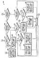
図1は、本発明の一実施形態に従ったデータ処理システム100をブロック図形式で示す。データ処理システム100は、メモリ166、バス168及びプロセッサ184を含む。データ処理システム100は、図示された構成要素以外の他の構成要素を含み得て、又は図示された構成要素より多くの又は少ない構成要素を含み得る。例えば、データ処理システム100は、任意の数のメモリ、周辺装置、又はプロセッサを含み得る。  FIG. 1 illustrates in block diagram form adata processing system 100 in accordance with one embodiment of the present invention.Data processing system 100 includesmemory 166, bus 168, andprocessor 184.Data processing system 100 may include other components than the illustrated components, or may include more or fewer components than the illustrated components. For example, thedata processing system 100 may include any number of memories, peripheral devices, or processors.

プロセッサ184は、命令レジスタ(IR)116、分岐アドレス計算器(BAC)108、プログラム・カウンタ112、マルチプレクサ(MUX)126、ラッチ160、加算器156、マルチプレクサ(MUX)154、分岐先バッファ(BTB)144、復号及び制御論理(DCL)164、命令バッファ105、比較器170、制御論理172及びプリフェッチ・バッファ102を含む。プリフェッチ・バッファ102は、命令スロットS0,S1,S2,S3,S4及びS5を含む。命令バッファ105は、プリフェッチ・バッファ102及び命令レジスタ116を含む。プロセッサ184は、例えば、マイクロプロセッサ、マイクロコントローラ、ディジタル信号プロセッサ等のようないずれのタイプのプロセッサであり得る。一実施形態においては、プロセッサ184は、プロセッサ・コアと呼ばれ得る。別の実施形態においては、プロセッサ184は、マルチプロセッサ・データ処理システムの中の多くのプロセッサのうちの1つであり得る。更に、プロセッサ184は、パイプライン化されたプロセッサであり得る。  Theprocessor 184 includes an instruction register (IR) 116, a branch address calculator (BAC) 108, aprogram counter 112, a multiplexer (MUX) 126, alatch 160, anadder 156, a multiplexer (MUX) 154, and a branch target buffer (BTB). 144, decode and control logic (DCL) 164,instruction buffer 105,comparator 170,control logic 172 andprefetch buffer 102.Prefetch buffer 102 includes instruction slots S0, S1, S2, S3, S4 and S5. Theinstruction buffer 105 includes aprefetch buffer 102 and aninstruction register 116. Theprocessor 184 can be any type of processor such as, for example, a microprocessor, microcontroller, digital signal processor, and the like. In one embodiment,processor 184 may be referred to as a processor core. In another embodiment, theprocessor 184 can be one of many processors in a multiprocessor data processing system. Further, theprocessor 184 may be a pipelined processor.

データ処理システム100の一実施形態において、プリフェッチ・バッファ102は、BAC108、DCL164、命令レジスタ116、及びバス168に結合されている。BAC108は、MUX126、プログラム・カウンタ112、プリフェッチ・バッファ102、及び命令レジスタ116に結合されている。MUX126は、プログラム・カウンタ112、BAC108、MUX154、加算器156、ラッチ160、及びバス168に結合されている。BTB144は、CTRL172、比較器170、及びMUX154に結合されている。比較器170は、MUX154、BTB144、アドレス・バス128、及びDCL164に結合されている。DCL164は、MUX126、命令レジスタ116、比較器170、プリフェッチ・バッファ102、メモリ166、及びCTRL172に結合されている。メモリ166は、バス168、及びDCL164に結合されている。  In one embodiment ofdata processing system 100,prefetch buffer 102 is coupled toBAC 108,DCL 164,instruction register 116, and bus 168. BAC 108 is coupled to MUX 126,program counter 112,prefetch buffer 102, andinstruction register 116. MUX 126 is coupled toprogram counter 112, BAC 108, MUX 154,adder 156,latch 160, and bus 168. BTB 144 is coupled toCTRL 172,comparator 170, and MUX 154.Comparator 170 is coupled to MUX 154, BTB 144,address bus 128, andDCL 164.DCL 164 is coupled to MUX 126,instruction register 116,comparator 170,prefetch buffer 102,memory 166, andCTRL 172.Memory 166 is coupled to bus 168 andDCL 164.

本発明の一実施形態において、メモリ166は、各命令が対応の命令アドレスを有する一連の命令を含む。プロセッサ184のクロック・サイクル中に、DCL164は、命令バッファ105がメモリ166からの所定数の命令を格納するため利用可能な所定数のスロットを有するかどうかを決定する。DCL164は、そのDCL164がプリフェッチ・バッファ102のサイズ、命令バッファ105の中の確保されたスロットの数、及びバス168を介してメモリから現在フェッチされている命令の数を知っていることを用いることにより命令バッファ105の中の利点可能な所定数のスロットが有るかどうかを決定することができる。所定数のスロットは、用いられているパイプライン化されたプロセッサに応じて変わり、そしてフェッチされた命令の数及びフェッチされている各命令のサイズに依存し得る。本明細書で説明される実施形態については、パイプライン化されたプロセッサがダブルワード・フェッチ・サイズを用い、所定数のスロットが2であり、且つフェッチされている命令の所定数が2であり、即ち2ワード・サイズ命令が各ダブルワード命令フェッチ中に要求されることを仮定する。代替実施形態は、本明細書で説明される実施形態以外の、異なる数のプリフェッチ・スロットを用い得て、また異なるパイプラインを用い得て、更にまた異なるフェッチ・サイズ及びメモリ・レイテンシー(待ち時間)を有し得る。  In one embodiment of the present invention,memory 166 includes a series of instructions, each instruction having a corresponding instruction address. During theprocessor 184 clock cycle, the DCL 164 determines whether theinstruction buffer 105 has a predetermined number of slots available to store a predetermined number of instructions from thememory 166. The DCL 164 uses that DCL 164 knows the size of theprefetch buffer 102, the number of reserved slots in theinstruction buffer 105, and the number of instructions currently being fetched from memory via the bus 168. Can determine whether there are a predetermined number of slots in theinstruction buffer 105 that can be advantageous. The predetermined number of slots varies depending on the pipelined processor being used and may depend on the number of instructions fetched and the size of each instruction being fetched. For the embodiments described herein, the pipelined processor uses a doubleword fetch size, the predetermined number of slots is 2, and the predetermined number of instructions being fetched is 2. That is, assume that a 2-word size instruction is required during each doubleword instruction fetch. Alternative embodiments may use a different number of prefetch slots, use different pipelines, and also have different fetch sizes and memory latencies (latencies) other than the embodiments described herein. ).

本発明の少なくとも1つの実施形態において、プリフェッチ・バッファ102を用いて、プロセッサ184による順次命令の実行に先立ってその順次命令を保持する。命令レジスタ116を用いて、実行のため復号されている現在の命令を保持する。命令が実行されるにつれ、順次命令は、プリフェッチ・バッファ・スロット0から又はデータ・バス130から導体114を介して命令レジスタ116に与えられる。これらの命令がパイプラインを通って進むにつれ、フェッチされた命令は、有効な命令が前のスロットに存在すると仮定すると、スロット1からスロット0にシフトされ、スロット2からスロット1にシフトされ、以下同様にされる。プリフェッチ・バッファ102の中の空のスロットは、バス168及びデータ・バス130を介してメモリ166からフェッチされた要求された命令で充填される。  In at least one embodiment of the invention,prefetch buffer 102 is used to hold the sequential instructions prior to execution of sequential instructions byprocessor 184.Instruction register 116 is used to hold the current instruction being decoded for execution. As instructions are executed, sequential instructions are provided to instruction register 116 fromprefetch buffer slot 0 or fromdata bus 130 viaconductor 114. As these instructions progress through the pipeline, the fetched instructions are shifted fromslot 1 toslot 0, shifted fromslot 2 toslot 1, assuming a valid instruction is in the previous slot, and so on. The same is done. Empty slots inprefetch buffer 102 are filled with requested instructions fetched frommemory 166 via bus 168 anddata bus 130.

本発明の少なくとも1つの実施形態においては、プリフェッチ・バッファ102は、命令レジスタ116からのメモリの減結合を可能にし、そして命令のFIFOとして働く。命令実行ストリームが命令の流れの変更なしで順次的なままであるある限り、命令は、順次的に要求され、プリフェッチ・バッファ102に供給され続ける。命令の流れの変更が起きるとき、順次命令ストリームは、廃棄されねばならず、そしてプリフェッチ・バッファ102は、未使用の順次命令をフラッシュされ、そして命令の流れの変更の目標位置から命令の新しいストリームで充填される。割り込み及び例外処理のような追加の事象がまた命令の流れの変更を起こさせるにも拘わらず、分岐命令をプロセッサ184で通常用いて、新しい命令ストリームへの命令の流れの変更を起こさせる。現在の命令ストリームが廃棄され、そして新しい命令ストリームが確立されたので、命令の流れの変更は、プロセッサ184での命令の正規の実行の破壊を起こす。これは、典型的には、プロセッサ184に、新しい命令ストリームが確立されるのを待ちながら1又はそれより多くのサイクルの命令の実行を停止(stall)させ、こうしてデータ処理システム100の全体的性能及び効率を低下させる。  In at least one embodiment of the present invention,prefetch buffer 102 allows decoupling of memory frominstruction register 116 and serves as an instruction FIFO. As long as the instruction execution stream remains sequential without changing the instruction flow, instructions are requested sequentially and fed to theprefetch buffer 102. When an instruction flow change occurs, the sequential instruction stream must be discarded, and theprefetch buffer 102 is flushed with unused sequential instructions and a new stream of instructions from the target position of the instruction flow change. Filled with. Although additional events such as interrupts and exception handling also cause instruction flow changes, branch instructions are typically used in theprocessor 184 to cause instruction flow changes to a new instruction stream. Since the current instruction stream has been discarded and a new instruction stream has been established, the change in instruction flow causes a disruption of the normal execution of instructions in theprocessor 184. This typically causes theprocessor 184 to stall execution of one or more cycles of instructions while waiting for a new instruction stream to be established, and thus the overall performance of thedata processing system 100. And reduce efficiency.

プリフェッチ・バッファ102の別の利点は、そのバッファのコンテンツ(中味)が、走査されて、プロセッサ184による分岐命令の実行に先立って、命令の流れの変更を生じさせ得る分岐命令の存在を決定し得ることである。実行に先立って命令ストリームを調べることにより、分岐命令はそれが実行される前の十分早期に検出され得ることが可能であり、そのためプロセッサ184に機能停止(stall)させること無しに目標命令ストリームを確立することができ、こうしてデータ処理システム100の実行効率を改善する。これは、「分岐先取り」を実行することとして知られている。機能停止条件を回避するため要求される先取りの深さは、プロセッサのパイプライン深さ及びメモリ・アクセス・レイテンシー(メモリ・アクセス待ち時間)の関数であり、そして本発明の様々な実施形態で変わり得る。  Another advantage of theprefetch buffer 102 is that the contents (content) of that buffer is scanned to determine the presence of a branch instruction that can cause an instruction flow change prior to execution of the branch instruction by theprocessor 184. Is to get. By examining the instruction stream prior to execution, the branch instruction can be detected sufficiently early before it is executed so that the target instruction stream is not stalled without causing theprocessor 184 to stall. Thus improving the execution efficiency of thedata processing system 100. This is known as performing a “branch prefetch”. The required preemption depth to avoid outage conditions is a function of processor pipeline depth and memory access latency, and will vary in various embodiments of the invention. obtain.

以下で更に説明されるであろう本発明の一実施形態においては、先取りの深さは、分岐命令が実行のため命令レジスタ116に到着する前の2つの命令に等しい。分岐先(分岐目標)(branch target)が、計算され、そしてアクセス要求が、メモリになされて、その分岐が実行のため命令レジスタに到着する前の少なくとも2命令サイクルで目標命令ストリームを獲得する場合、追加の機能停止条件がプロセッサ184に関して引き起こされないであろう。これは、分岐命令がプリフェッチ・バッファ102のスロット(S1)で検出される場合達成されることができる。それは、2つの命令が、即ちスロット0(S0)の中及び命令レジスタ116の中のそれらの命令が分岐命令より前にあるからである。この場合、分岐先が、計算され得て、そして要求が、メモリに対してなされて、目標命令を獲得し、それは、目標命令ストリームにアクセスする際に被る遅延に起因した追加の実行停止サイクルを回避するためプロセッサ184に適時に戻るであろう。  In one embodiment of the invention, which will be further described below, the prefetch depth is equal to two instructions before the branch instruction arrives at theinstruction register 116 for execution. A branch target is calculated and an access request is made to memory to obtain the target instruction stream in at least two instruction cycles before the branch arrives at the instruction register for execution , No additional outage conditions will be triggered for theprocessor 184. This can be achieved if a branch instruction is detected in slot (S1) ofprefetch buffer 102. That is because there are two instructions, namely those in slot 0 (S0) and in theinstruction register 116 before the branch instruction. In this case, the branch destination can be calculated and a request is made to the memory to obtain the target instruction, which causes an additional stop cycle due to the delay incurred in accessing the target instruction stream. It will return in a timely manner to theprocessor 184 to avoid.

全ての分岐命令がプリフェッチ・バッファ102のスロット1の中で検出可能であるわけではないことがあり得る。それは、分岐命令がスロット1をバイパスし、そして直接に命令レジスタ116に又はプリフェッチ・バッファ102のスロット0にデータ・バス130を介してロードされ得るからである。これらの条件は、命令の流れの変更が生じたとき生じ、そして目標命令ストリームは、分岐命令を新しいストリームのヘッド近くに含む。最初の2つの戻り命令が命令レジスタ116及びプリフェッチ・バッファ102のスロット0にロードされるので、それらは、プリフェッチ・バッファ102のスロット1に常駐してなく、従って、第2の目標命令ストリームが到着するのを待ちながらプロセッサ184の機能停止を回避するため十分早期に命令の流れの第2の変更の目標をフェッチする機会が存在しなかったであろう。その上、プロセッサ184が第3及び第4の命令が目標ストリームから到着するのを待ちながら命令の実行を完了した場合、命令パイプラインは、進行し、そして第3及び第4の戻り命令は、プリフェッチ・バッファ102のスロット1及びスロット2ではなくスロット0及びスロット1に配置されるであろう。分岐命令が新しい目標ストリームの第3の命令として存在する場合、その分岐命令は、スロット1に存在する機会を持たず、従って、分岐先取りのみを用いて、次の目標ストリームをフェッチし且つプロセッサ184の機能停止を回避するため不十分な時間しか使用可能でないであろう。  Not all branch instructions may be detectable inslot 1 ofprefetch buffer 102. This is because a branch instruction bypassesslot 1 and can be loaded either directly intoinstruction register 116 or intoslot 0 ofprefetch buffer 102 viadata bus 130. These conditions occur when an instruction flow change occurs and the target instruction stream contains a branch instruction near the head of the new stream. Since the first two return instructions are loaded intoinstruction register 116 andslot 0 ofprefetch buffer 102, they are not resident inslot 1 ofprefetch buffer 102, so the second target instruction stream has arrived. There would have been no opportunity to fetch the target of the second change in instruction flow sufficiently early to avoid theprocessor 184 stalling while waiting to do so. Moreover, if theprocessor 184 completes execution of instructions while waiting for the third and fourth instructions to arrive from the target stream, the instruction pipeline proceeds and the third and fourth return instructions are: It will be placed inslot 0 andslot 1 instead ofslot 1 andslot 2 ofprefetch buffer 102. If a branch instruction exists as the third instruction of the new target stream, the branch instruction has no opportunity to exist inslot 1 and therefore uses only branch prefetch to fetch the next target stream andprocessor 184. Insufficient time will be available to avoid the outage.

他の実施形態においては、分岐命令は、他の理由のためプリフェッチ・バッファ102のスロット1をヒットしないことがあり得る。例えば、統一メモリ・バス(unified memory bus)を有するデータ処理システムは、連続的ロード/ストア命令を実行しながら命令バッファ105を排出(drain)することができるであろう。命令バッファ105の中のこのロード/ストア命令を実行した後で命令レジスタ及びスロット0を充填するための後続のフェッチは、後続の分岐命令がプリフェッチ・バッファ102のスロット1で処理されないことをもたらすことができるであろう。  In other embodiments, the branch instruction may not hitslot 1 ofprefetch buffer 102 for other reasons. For example, a data processing system having a unified memory bus could drain theinstruction buffer 105 while executing sequential load / store instructions. Subsequent fetches to fill the instruction register andslot 0 after executing this load / store instruction ininstruction buffer 105 result in the subsequent branch instruction not being processed inslot 1 ofprefetch buffer 102. Will be able to.

たとえ分岐命令が追加の機能停止条件を含むことを回避するため十分早期にスロット1に到着しなくても、分岐命令がプリフェッチ・バッファ102のスロット0にある間に分岐先アドレスを計算し且つ目標命令ストリームを要求することにより分岐を部分的に加速する機会が依然としてあり得る。この場合、1又はそれより多くのサイクルの機能停止が回避されるであろう。  Even if the branch instruction does not arrive inslot 1 early enough to avoid including an additional outage condition, the branch destination address is calculated while the branch instruction is inslot 0 of theprefetch buffer 102 and the target There may still be an opportunity to partially accelerate the branch by requesting an instruction stream. In this case, outage of one or more cycles will be avoided.

たとえ分岐命令が命令バッファ105のスロット1にロードされることができても、その特定の分岐命令のため目標ストリームをフェッチし始める機会がないかも知れない。それは、異なる分岐命令がまたスロット0又は命令レジスタ116に存在することが可能であるからである。この場合、一実施形態において、命令レジスタ116の中のより早期の分岐は、たとえそのより早期の命令が分岐条件に適合しない場合実際に取られることができなくてもメモリ・アクセスに関するより高い優先度を与えられるであろう。この場合、第1の分岐のための目標命令ストリームは、廃棄されるが、しかしプリフェッチ・バッファ102のスロット1に存在(resident)する次の分岐のため目標ストリームをフェッチする機会を逸してしまうであろう。  Even if a branch instruction can be loaded intoslot 1 ofinstruction buffer 105, there may not be an opportunity to begin fetching the target stream for that particular branch instruction. This is because different branch instructions can also be present inslot 0 orinstruction register 116. In this case, in one embodiment, an earlier branch in theinstruction register 116 has a higher priority for memory access even if the earlier instruction cannot actually be taken if the branch condition does not meet the branch condition. Will be given a degree. In this case, the target instruction stream for the first branch is discarded, but misses the opportunity to fetch the target stream for the next branch present inslot 1 of theprefetch buffer 102. I will.

命令の流れの来るべき変更を十分早期に検出することができそして要求が目標ストリームをフェッチするためメモリに対してなされる場合分岐先取り技術を用いることによりプロセッサ184の機能停止条件を低減させることができることが分かることができるが、しかしそれができない場合が頻繁にある。この場合に関しては、分岐先バッファを用いて、分岐命令の目標ストリームにアクセスすることを加速する。本発明の一実施形態において、BTB144は、そのBTB144に前に格納された分岐命令のため、事前計算された目標アドレスを保持する。目標アドレスの計算は時間を必要とするので、一実施形態においては、目標アドレスは、分岐先取り技術を用いる場合より1又はそれより多くのクロック・サイクルだけ早期に要求されることができる。目標アドレスを含むBTBエントリが使用可能である場合、目標命令ストリームは、分岐がプリフェッチ・バッファ102に又は命令レジスタ116に到着する前に確立されることができる。分岐命令のアドレスを用いて、BTB144の中のルックアップを実行して、マッチング・エントリが存在するかどうかを決定することができる。マッチング・エントリが存在する場合、目標アドレスが、BTB144から獲得され、そしてメモリ要求を行って、その命令を分岐先位置(分岐目標位置)(branch target location)で獲得し得る。  An upcoming change in instruction flow can be detected early enough and reducing the outage condition ofprocessor 184 by using a branch prefetch technique when a request is made to memory to fetch the target stream. You can see that you can, but often you can't. In this case, the branch destination buffer is used to accelerate access to the target stream of the branch instruction. In one embodiment of the present invention, the BTB 144 maintains a precomputed target address for the branch instruction previously stored in that BTB 144. Since the target address calculation is time consuming, in one embodiment, the target address can be requested earlier by one or more clock cycles than when using a branch prefetch technique. If the BTB entry containing the target address is available, the target instruction stream can be established before the branch arrives at theprefetch buffer 102 or theinstruction register 116. Using the address of the branch instruction, a lookup in BTB 144 can be performed to determine if a matching entry exists. If there is a matching entry, the target address is obtained from the BTB 144 and a memory request can be made to obtain the instruction at the branch target location.

BTB144は、分岐命令の目標アドレスを格納するため限定数のエントリを含む。データ処理システム100の最高性能のため、追加のプロセッサ184の機能停止を起こすことなしにプリフェッチ・バッファ102における分岐先取りにより加速されることができるそれらの分岐は、BTB144における1つのエントリを割り当てられないで、従ってBTB144の「実効的」容量を増大する。  The BTB 144 includes a limited number of entries to store the target address of the branch instruction. For the best performance of thedata processing system 100, those branches that can be accelerated by branch prefetch in theprefetch buffer 102 without causing anadditional processor 184 outage will not be assigned one entry in the BTB 144. Thus increasing the "effective" capacity of the BTB 144.

複数の分岐命令が命令レジスタ116及びプリフェッチ・バッファ102の中に存在し得るので、復号及び制御論理164は、アクセスされるべき分岐先ストリームの選択を優先順位付けしなければならない。本発明の一実施形態において、命令レジスタの中の分岐命令は、最高位に優先順位付けされ、プリフェッチ・バッファ102のスロット0は、次の最高位に優先順位付けされ、プリフェッチ・バッファ102のスロット1がその次に高い優先順位に付けられ、以下同様に優先順位付けされる。それは、これが命令ストリームの中の命令の論理的順序を表すからである。DCL164は、こうして命令レジスタ116で始まって、プリフェッチ・バッファ102のスロット0、次いでスロット1と逆順に命令を走査する。分岐命令がより高い優先順位の位置に見つけられた場合、より低い優先順位の位置の分岐命令は、一時的に無視される。  Since multiple branch instructions may exist ininstruction register 116 andprefetch buffer 102, decode and controllogic 164 must prioritize the selection of the branch destination stream to be accessed. In one embodiment of the invention, the branch instruction in the instruction register is prioritized to the highest order,slot 0 of theprefetch buffer 102 is prioritized to the next highest order, and the slot of theprefetch buffer 102 1 is given the next highest priority, and so on. This is because it represents the logical order of instructions in the instruction stream. TheDCL 164 thus scans for instructions in reverse order starting with theinstruction register 116 inslot 0 of theprefetch buffer 102 and then inslot 1. If a branch instruction is found at a higher priority position, the lower priority position branch instruction is temporarily ignored.

DCL164が命令レジスタ116に置かれた命令が分岐命令でないと決定したとき、ロードBTB174(BTB174にロード)は、ディアサートされたままである。BTB更新は、分岐が実際に取られることを決定された後でのみ実行され、そしてこれは、分岐命令が命令レジスタ116に到着するまでに必ずしも決定されるわけではない。  WhenDCL 164 determines that the instruction placed ininstruction register 116 is not a branch instruction, load BTB 174 (load to BTB 174) remains deasserted. A BTB update is performed only after it is determined that the branch is actually taken, and this is not necessarily determined before the branch instruction arrives at theinstruction register 116.

本発明の少なくとも1つの実施形態において、DCL164はまた、条件付き分岐の成果を予測するため用いられる分岐予測論理を含む。条件付き分岐を取った成果又は取らなかった成果に関する予測に応じて、目標命令ストリームは、プリフェッチされ得て、又は、或る実施形態においては、分岐条件が実際に解決(resolve)されるまでプリフェッチされることが遅らされる。本発明の代替実施形態は、分岐予測論理をBTB144において、又はプロセッサ184における他の位置において実現し得て、又は分岐予測論理を利用しない場合も有り得る。分岐予測論理を用いないとき、或る実施形態においては、分岐先位置が、分岐条件が解決されることを待つことなしにプリフェッチされ、それは、分岐先位置をプリフェッチする目的のため分岐が取られるであろうことを予測することと等価である。  In at least one embodiment of the invention,DCL 164 also includes branch prediction logic that is used to predict the outcome of conditional branches. Depending on the prediction about the outcome taken or not taken, the target instruction stream can be prefetched or, in some embodiments, prefetched until the branch condition is actually resolved. To be delayed. Alternative embodiments of the present invention may implement branch prediction logic at BTB 144, or elsewhere inprocessor 184, or may not utilize branch prediction logic. When not using branch prediction logic, in some embodiments, the branch destination location is prefetched without waiting for the branch condition to be resolved, which is taken for the purpose of prefetching the branch destination location. Is equivalent to predicting that

本発明の一実施形態において、分岐アドレス計算器108を用いて、プリフェッチ・バッファ102の中の命令のスロット目標アドレスと、命令レジスタ116の中の命令の命令レジスタ目標アドレスとを決定し得る。例えば、クロック・サイクル中に、分岐アドレス計算器108は、プリフェッチ・バッファ102及び命令レジスタ116に格納された命令の変位フィールドと、プログラム・カウンタPC112から現在実行されている命令のアドレスとを受信する。次いで、分岐アドレス計算器108は、スロット0の中の命令のスロット0目標アドレス(S0TA)、スロット1の中の命令のスロット1目標アドレス(S1TA)、及び命令レジスタ116の中の命令の命令レジスタ目標アドレス(IRTA)を計算する。IRTA、S0TA、S1TA等のうちのいるかは、以下で更に説明される用に、DCL164が命令バッファ105に格納された命令が分岐命令であるとき選択される。  In one embodiment of the present invention,branch address calculator 108 may be used to determine the slot target address for instructions inprefetch buffer 102 and the instruction register target address for instructions ininstruction register 116. For example, during a clock cycle,branch address calculator 108 receives the instruction displacement field stored inprefetch buffer 102 andinstruction register 116 and the address of the instruction currently being executed fromprogram counter PC 112. . Thebranch address calculator 108 then selects theslot 0 target address (S0TA) for the instruction inslot 0, theslot 1 target address (S1TA) for the instruction inslot 1, and the instruction register for the instruction in theinstruction register 116. Calculate the target address (IRTA). Which of IRTA, S0TA, S1TA, etc. is selected when the instruction stored in theinstruction buffer 105 is a branch instruction forDCL 164 for further explanation below.

図1に示される本発明の少なくとも1つの実施形態の動作が、図2及び図3に示されるフロー図を参照して以下で説明されるであろう。本発明の一実施形態において、フローは、開始の長円形205で始まり、そして判断の菱形210に進んで、分岐命令がIR116にあるかどうかを決定する。この決定の結果が肯定(イエス)である場合、フローは、判断の菱形215に進み、そこで分岐命令がIR116に到着する前にプリフェッチ・バッファ102のスロット1の中に以前にプリフェッチされたかどうかが決定される。この決定の結果が肯定(イエス)である場合、フローは、判断の菱形267に進んで、分岐命令が要求されたかどうかを決定する。この決定の結果が肯定(イエス)である場合、フローは、ステップ295に進み、そこで、新しいBTB144エントリが割り当てられてなく、そして目標位置が到着するのを待つ。次いで、フローは、次のサイクルの長円形260に進んで、次のサイクルを始める。この場合、目標がプリフェッチ・バッファ102のスロット1からプリフェッチされ且つプロセッサ184に適時に到着していずれの追加の機能停止サイクルを回避し得るので、IR116の中の分岐のために新しいBTB144エントリを割り当てる必要性がない。  The operation of at least one embodiment of the invention shown in FIG. 1 will be described below with reference to the flow diagrams shown in FIGS. In one embodiment of the present invention, the flow begins with a starting oval 205 and proceeds to adecision diamond 210 to determine whether a branch instruction is in theIR 116. If the result of this determination is affirmative (yes), flow proceeds todecision diamond 215 where it is determined whether the branch instruction was previously prefetched intoslot 1 ofprefetch buffer 102 before arriving atIR 116. It is determined. If the result of this determination is affirmative (yes), flow proceeds todecision diamond 267 to determine whether a branch instruction has been requested. If the result of this determination is affirmative (yes), the flow proceeds to step 295 where a new BTB 144 entry has not been assigned and waits for the target position to arrive. The flow then proceeds to thenext cycle oval 260 to begin the next cycle. In this case, the target is prefetched fromslot 1 ofprefetch buffer 102 and arrives atprocessor 184 in time to avoid any additional outage cycles, so a new BTB 144 entry is allocated for the branch inIR 116 There is no need.

判断の菱形267に戻って、分岐先が前に要求されなかった場合、フローは、判断の菱形270に進んで、分岐命令のためのBTBヒットがあったかどうかを決定する。その決定が肯定(イエス)である場合、フローは、ステップ275に進み、そこで、BTBルックアップの結果をいずれの分岐予測論理の結果と一緒に用いて、目標位置を予測する。次いで、フローは、次のサイクルの長円形260に進む。判断の菱形270における決定がBTBヒットがなかったことである場合、フローは、判断の菱形280に進んで、プロセッサが機能停止されたかどうかを決定する。プロセッサは、マルチサイクル命令からのデータ依存性を含む任意の数の理由のため機能停止し得る。上記の決定が肯定(イエス)である場合、フローは、ステップ290に進み、そこで、目標位置は、分岐予測論理の結果に基づいてプリフェッチされ、そしてBTBエントリは、割り当てられない。この場合、プロセッサ184の機能停止は、BTBエントリを要求することなしに、分岐先位置を獲得するのに十分な時間を与え得て、従って新しいエントリを割り当てる必要性を回避する。これは、BTBの一層の効率的使用をもたらす。次いで、フローは、次のサイクルの長円形260に進む。  Returning todecision diamond 267, if a branch destination was not previously requested, flow proceeds todecision diamond 270 to determine if there was a BTB hit for the branch instruction. If the decision is affirmative (yes), flow proceeds to step 275 where the result of the BTB lookup is used along with the result of any branch prediction logic to predict the target location. The flow then proceeds to thenext cycle oval 260. If the decision atdecision diamond 270 is that there was no BTB hit, flow proceeds todecision diamond 280 to determine if the processor has been deactivated. The processor can stall for any number of reasons, including data dependencies from multi-cycle instructions. If the above decision is affirmative (yes), flow proceeds to step 290 where the target location is prefetched based on the result of the branch prediction logic and no BTB entry is assigned. In this case, the outage ofprocessor 184 may provide sufficient time to acquire the branch target location without requiring a BTB entry, thus avoiding the need to allocate a new entry. This results in a more efficient use of BTB. The flow then proceeds to thenext cycle oval 260.

判断の菱形280に戻って、プロセッサ184の機能停止がない場合、フローは、ステップ285に進み、そこで、目標位置は、分岐予測論理の結果に基づいてプリフェッチされ、そして新しいBTBエントリは、分岐が取られるよう解決される場合割り当てられる。この場合、BTBエントリの割り当ては、この特定の分岐に遭遇する次の時に改善された分岐性能を可能にする。次いで、フローは、次のサイクルの長円形260に進む。  Returning todecision diamond 280, if there is noprocessor 184 outage, the flow proceeds to step 285 where the target position is prefetched based on the result of the branch prediction logic and the new BTB entry is Assigned when resolved to be taken. In this case, BTB entry allocation allows improved branch performance the next time this particular branch is encountered. The flow then proceeds to thenext cycle oval 260.

判断の菱形215に戻って、分岐命令がプリフェッチ・バッファ102のスロット1の中にプリフェッチされなかった場合、フローは、判断の菱形220に進み、そこで、分岐命令がプリフェッチ・バッファ102のスロット0の中にプリフェッチされたかどうかの決定が行われる。その決定の結果が否定(ノー)である場合、フローは、判断の菱形225に進み、そこで、BTBヒットが生じたかどうかの決定が行われる。BTBヒットが生じなかった場合、フローは、ステップ230に進み、そこで、分岐先は、分岐予測論理の結果に基づいてプリフェッチされ、そして新しいBTBエントリは、分岐が取られるよう解決された場合割り当てられる。この場合、BTBエントリの割り当ては、この特定の分岐に遭遇する次の時に改善された分岐性能を可能にする。次いで、フローは、次のサイクルの長円形260に進む。  Returning todecision diamond 215, if the branch instruction was not prefetched intoslot 1 ofprefetch buffer 102, flow proceeds todecision diamond 220 where the branch instruction is inslot 0 ofprefetch buffer 102. A determination is made whether it has been prefetched into. If the result of the decision is negative (no), flow proceeds todecision diamond 225 where a determination is made whether a BTB hit has occurred. If no BTB hit occurred, flow proceeds to step 230 where the branch destination is prefetched based on the result of the branch prediction logic and a new BTB entry is assigned if the branch is resolved to be taken. . In this case, BTB entry allocation allows improved branch performance the next time this particular branch is encountered. The flow then proceeds to thenext cycle oval 260.

判断の菱形225によりBTBヒットが生じた決定された場合、フローは、ステップ275に進み、そして、ステップ275の動作に関して前に説明したように動作が続行される。  If thedecision diamond 225 determines that a BTB hit has occurred, the flow proceeds to step 275 and operation continues as previously described with respect to the operation ofstep 275.

判断の菱形220に戻って、分岐命令がプリフェッチ・バッファ102のスロット0の中にプリフェッチされた場合、フローは、判断の菱形222に進み、そこで、分岐先がスロット0から要求されたかどうかの決定が行われる。分岐先位置が要求された場合、フローは、判断の菱形226に進んで、プロセッサの機能停止条件があるかどうかを決定する。プロセッサの機能停止条件がある場合、フローは、ステップ295に進み、そして、ステップ295の動作に関して前に説明したように動作が続行する。プロセッサの機能停止条件がない場合、フローは、ステップ300に進み、そして、新しいBTBエントリは、分岐が取られるよう解決された場合条件付きで割り当てられ、そして、プロセッサは、目標が到着するのを待つ。判断の菱形222により分岐先位置が要求されなかったと決定された場合、フローは、判断の菱形224に進み、そこで、BTBヒットがあったかどうかの決定が行われる。BTBヒットがあった場合、フローは、ステップ275に進み、そして、ステップ275の動作に関して前に説明されたように動作が続行される。  Returning todecision diamond 220, if a branch instruction is prefetched intoslot 0 ofprefetch buffer 102, flow proceeds todecision diamond 222 where a determination is made whether a branch destination was requested fromslot 0. Is done. If a branch destination location is requested, flow proceeds todecision diamond 226 to determine if there is a processor outage condition. If there is a processor outage condition, flow proceeds to step 295 and operation continues as previously described with respect to the operation ofstep 295. If there is no processor outage condition, flow proceeds to step 300 and a new BTB entry is conditionally assigned if the branch is resolved to be taken, and the processor waits for the target to arrive. wait. If thedecision diamond 222 determines that a branch destination location was not requested, the flow proceeds to thedecision diamond 224 where a determination is made whether there was a BTB hit. If there is a BTB hit, flow proceeds to step 275 and operation continues as previously described with respect to the operation ofstep 275.

判断の菱形224によりBTBヒットがなかったと決定された場合、フローは、判断の菱形280に進んで、プロセッサ184の機能停止条件が存在するかどうかを決定し、そして、ステップ280の動作に関して前に説明したように動作が続行する。  Ifdecision diamond 224 determines that there was no BTB hit, flow proceeds todecision diamond 280 to determine if aprocessor 184 outage condition exists, and before the operation ofstep 280 Operation continues as described.

判断の菱形210に戻って、分岐がIR116の中にない場合、フローは、判断の菱形235に進み、そこで、プリフェッチ・バッファ102のスロット0の中に分岐命令があるかどうかを決定する。その決定の結果が肯定(イエス)である場合、フローは、判断の菱形265に進んで、スロット0の中の分岐命令がスロット1の中にプリフェッチされたかどうかを決定する。分岐命令がスロット1の中にプリフェッチされた場合、フローは、判断の菱形267に進み、そして、判断の菱形267の動作に関して前に説明したように動作が続行する。分岐命令がスロット1の中にプリフェッチされなかった場合、フローは、判断の菱形270に進み、そして、判断の菱形270の動作に関して前に説明したように動作が続行する。判断の菱形235における決定の結果が否定(ノー)である場合、フローは、判断の菱形240に進み、そこで、プリフェッチ・バッファ102のスロット1の中に分岐命令があるかどうかを決定する。その決定の結果が否定(ノー)である場合、フローは、分岐命令が命令バッファ105の位置の所定のサブセットの中に見つけられなかったので次のサイクルの長円形260に進む。判断の菱形240における決定の結果がプリフェッチ・バッファ102のスロット1の中に分岐命令があることである場合、一実施形態においては、フローは、判断の菱形245に進んで、BTBヒットがスロット1の中の分岐命令のため生じたかどうかを決定する。BTBヒットが生じた場合、フローは、ステップ255に進み、そしてBTBルックアップの結果及び分岐予測論理の結果を用いて、分岐先をプリフェッチする。次いで、フローは、次のサイクルの長円形260に進む。本発明の一実施形態においては、判断の菱形245の結果がBTBヒットが生じたことである場合、フローは、ステップ250に進んで、そこで、分岐先位置は、分岐予測論理に基づいてプリフェッチされ、そして新しいBTBエントリは、割り当てられない。代わりに、目標フェッチが、完了するため可能にされ、次いでフローは、次のサイクルの長円形260に進む。  Returning todecision diamond 210, if the branch is not inIR 116, flow proceeds todecision diamond 235 where it determines if there is a branch instruction inslot 0 ofprefetch buffer 102. If the result of the decision is affirmative (yes), flow proceeds todecision diamond 265 to determine if the branch instruction inslot 0 has been prefetched intoslot 1. If the branch instruction is prefetched intoslot 1, flow proceeds todecision diamond 267 and operation continues as previously described with respect to the operation ofdecision diamond 267. If the branch instruction was not prefetched intoslot 1, flow proceeds todecision diamond 270 and operation continues as previously described with respect to the operation ofdecision diamond 270. If the result of the decision atdecision diamond 235 is negative (no), flow proceeds todecision diamond 240 where it determines whether there is a branch instruction inslot 1 ofprefetch buffer 102. If the decision is negative (no), flow proceeds to thenext cycle oval 260 because the branch instruction was not found in the given subset ofinstruction buffer 105 locations. If the result of the decision atdecision diamond 240 is that there is a branch instruction inslot 1 ofprefetch buffer 102, in one embodiment, the flow proceeds todecision diamond 245 where the BTB hit isslot 1; Determine if it occurred because of a branch instruction in If a BTB hit occurs, the flow proceeds to step 255 and uses the BTB lookup result and the branch prediction logic result to prefetch the branch destination. The flow then proceeds to thenext cycle oval 260. In one embodiment of the present invention, if the result ofdecision diamond 245 is that a BTB hit has occurred, flow proceeds to step 250 where the branch destination location is prefetched based on the branch prediction logic. , And new BTB entries are not allocated. Instead, target fetching is enabled to complete, and then flow proceeds tooval 260 of the next cycle.

代替実施形態においては、図3におけるフローのステップ245が、除かれ、そしてフローは、ステップ240における「肯定(イエス)」の決定からステップ250に直接進み得る。これは、分岐先アドレスがスロット1で計算され、そして十分な時間が目標命令が到着するため使用可能であるならば目標命令ストリームがBTB144の支援無しにフェッチされるので起こり得る。  In an alternative embodiment, step 245 of the flow in FIG. 3 is removed, and the flow may proceed directly to step 250 from the “Yes” determination instep 240. This can occur because the branch destination address is calculated inslot 1 and the target instruction stream is fetched without BTB 144 assistance if sufficient time is available for the target instruction to arrive.

図2及び図3に示されるフローは、プロセッサ184のBTB144が最高の便利さを与えるため有利に動作され得る少なくとも1つのあり得る方法を表す。分岐先位置がBTB144を利用すること無しに獲得され、且つデータ処理システム100の動作に追加の遅延を招くことを依然回避し得る条件を決定することにより、より効率的な使用は、限定された容量のBTB144から生じ得る。  The flow shown in FIGS. 2 and 3 represents at least one possible method in which the BTB 144 of theprocessor 184 can be advantageously operated to provide maximum convenience. By determining the conditions where branch target locations are obtained without using BTB 144 and still can avoid incurring additional delays in the operation ofdata processing system 100, more efficient use is limited. It can result from a capacity BTB 144.

図1に示される本発明の少なくとも1つの実施形態の動作は、図4、図5、図6及び図7に示されるタイミング図、及び図2及び図3に示されるフロー図を参照して以下で説明されるであろう。図4及び図5に示されるそれぞれのタイミング図の最初のクロック・サイクルの始めに、ロードBTB174及び比較器一致信号197が、ディアサートされると仮定する。  The operation of at least one embodiment of the present invention shown in FIG. 1 is as follows with reference to the timing diagrams shown in FIGS. 4, 5, 6 and 7 and the flow diagrams shown in FIGS. Will be explained. Assume thatload BTB 174 andcomparator match signal 197 are deasserted at the beginning of the first clock cycle of the respective timing diagrams shown in FIGS.

図1に示される本発明の少なくとも1つの実施形態において、図4を参照すると、第1のクロック・サイクル中に、DCL164は、2つのスロットが命令バッファ105の中で使用可能であるかどうかを決定する。DCL164が2つのスロットが命令バッファ105、この場合、命令レジスタ116及びスロット0の中で使用可能であると決定したとき、要求信号199が、アサートされ、そしてその2つのスロット、即ち命令レジスタ116及びスロット0が、確保される。要求信号199が、DCL164からメモリ166に与えられ、そしてそれを用いて、命令がメモリ166からフェッチされることを要求する。フェッチされている初期命令に対応する命令アドレスは、プログラム・カウンタ112によりIIA123を介してMUX126に与えられる。DCL164は、MUX126を用いて、初期命令アドレス123を選択し、その初期命令アドレス123は、次いで、アドレス128上へ駆動されて、メモリ166の中のアドレス$0及びアドレス$4に配置された命令I0及びI1を要求する。  In at least one embodiment of the invention shown in FIG. 1, referring to FIG. 4, during the first clock cycle,DCL 164 determines whether two slots are available ininstruction buffer 105. decide. WhenDCL 164 determines that two slots are available ininstruction buffer 105, in this case,instruction register 116 andslot 0, request signal 199 is asserted, and the two slots,instruction register 116 andSlot 0 is reserved. Request signal 199 is provided fromDCL 164 tomemory 166 and is used to request that an instruction be fetched frommemory 166. The instruction address corresponding to the initial instruction being fetched is given to theMUX 126 by theprogram counter 112 via theIIA 123. TheDCL 164 uses theMUX 126 to select theinitial instruction address 123, which is then driven onto theaddress 128 to place the instructions located at addresses $ 0 and $ 4 in thememory 166. Request I0 and I1.

アドレス・バス128上へ駆動された命令アドレス$0は、ラッチ160、比較器170及びメモリ166に与えられる。ラッチ160は、アドレス・バス128及び加算器156に結合されていて、そのラッチ160は、アドレス・バス128上へ駆動された命令アドレスを捕捉する。次いで、加算器156は、現在の命令アドレスをダブルワード・フェッチ・サイズ$8だけ増分する。前述したように、ダブルワード・フェッチ・サイズは、本発明の異なる実施形態で変わり、そしてフェッチされている各命令のサイズに依存し得る。ラッチ160による捕捉、及び加算器156により生じるアドレス・バス128上のアドレスの増分は、全てのクロック・サイクル中に生じ、そこにおいては、アドレス・バス128上へ駆動されたアドレスがあり、そして要求が、メモリに対してなされる。増分されたアドレス、この場合、$8は、加算器156により順次命令アドレス(SIA)158として出力される。  The instruction address $ 0 driven ontoaddress bus 128 is provided to latch 160,comparator 170 andmemory 166.Latch 160 is coupled to addressbus 128 andadder 156, which latches the instruction address driven ontoaddress bus 128.Adder 156 then increments the current instruction address by a doubleword fetch size of $ 8. As previously mentioned, the doubleword fetch size varies in different embodiments of the present invention and may depend on the size of each instruction being fetched. The capture bylatch 160 and the increment of the address onaddress bus 128 caused byadder 156 occur during every clock cycle, where there is an address driven ontoaddress bus 128 and the request Is made to the memory. The incremented address, in this case $ 8, is sequentially output as an instruction address (SIA) 158 by theadder 156.

比較器170は、アドレス・バス128上へ駆動されたアドレスを受け取り、そしてそのアドレスを、もしあれば分岐先バッファ144に格納されている1つ又は複数の分岐命令アドレスと比較する。分岐先バッファ144は、メモリ166から受け取られた分岐命令のアドレスを格納するための分岐命令アドレス(BIA)スロットと、それらの分岐命令に対応する計算された目標アドレスを格納するための分岐先アドレス(BTA)と、フラグ・ビット(FB)スロットのアサートされた(有効な)又はディアサート(無効な)ビットが各分岐先アドレス・スロット及び対応の分岐先アドレス・スロットが有効な又は無効な分岐先アドレスを有するかどうかを表す当該フラグ・ビット(FB)スロットとを含む。分岐先アドレスがBTB144の中のBIAスロットにロードされ、そして対応の分岐先アドレスがBTB144の中の対応のBTAスロットにロードされるとき、関連したフラグ・ビットが、有効なBTBエントリを指示するようアサートされる。リセット時、スタートアップ時、及び分岐先アドレスがBIAスロットにないか又は対応の分岐先アドレスがBTB144の中のBTAスロットにない時、関連したフラグ・ビットは、ディアサートされる。フラグ・ビットは、BIA及びBTAが有効か又は無効かどうかを表すため、例えば、0又は1であり得る。  Comparator 170 receives the address driven ontoaddress bus 128 and compares the address, if any, to one or more branch instruction addresses stored in branch target buffer 144. Branch destination buffer 144 has branch instruction address (BIA) slots for storing addresses of branch instructions received frommemory 166, and branch destination addresses for storing calculated target addresses corresponding to those branch instructions. (BTA) and the flag bit (FB) slot asserted (valid) or deasserted (invalid) bit is valid for each branch destination address slot and the corresponding branch destination address slot is valid or invalid. And a corresponding flag bit (FB) slot indicating whether or not it has a destination address. When a branch destination address is loaded into a BIA slot in BTB 144 and a corresponding branch destination address is loaded into a corresponding BTA slot in BTB 144, the associated flag bit will indicate a valid BTB entry. Asserted. At reset, at startup, and when the branch target address is not in the BIA slot or the corresponding branch target address is not in the BTA slot in the BTB 144, the associated flag bit is deasserted. The flag bit can be, for example, 0 or 1 to indicate whether BIA and BTA are valid or invalid.

比較器170がアドレス・バス128上へ駆動されたアドレスがBTB144に格納されている分岐命令アドレスのいずれかと一致すると決定し、そして関連したフラグ・ビットが有効であるとき、BTBヒットが、生じており、そして比較器170は、比較器一致信号197をアサートする。比較器170はまた、信号180及びMUX154を用いて、BTBヒットを発生した分岐命令アドレスに対応する分岐先アドレスを選択する。選択された分岐先アドレスは、分岐先バッファ目標アドレス(BTBTA)178を用いて、MUX126に与えられる。比較器一致信号197がアサートされるので、DCL164は、BTBTA178を選択し、そして分岐先アドレスをアドレス・バス128上へ駆動する。  When thecomparator 170 determines that the address driven on theaddress bus 128 matches any of the branch instruction addresses stored in the BTB 144, and the associated flag bit is valid, a BTB hit occurs Andcomparator 170 assertscomparator match signal 197.Comparator 170 also usessignal 180 andMUX 154 to select the branch destination address corresponding to the branch instruction address that generated the BTB hit. The selected branch destination address is given to theMUX 126 using the branch destination buffer target address (BTBTA) 178. Ascomparator match signal 197 is asserted,DCL 164 selectsBTBTA 178 and drives the branch destination address ontoaddress bus 128.

比較器170がアドレス・バス128上へ駆動されたアドレスがBTB144の中のいずれの分岐命令アドレスとも一致しないこと又はアドレス・バス128上へ駆動されたアドレスがBTB144の中の分岐命令アドレスと一致することを決定するが、しかし一致されたBIAアドレスに対応するフラグ・ビットが無効であるとき、BTBミスが、生じており、そして比較器一致信号197は、比較器170によりディアサートされる。比較器一致信号197がディアサートされたとき、DCL164は、BTBTA178を、アドレス・バス128上へ駆動されるべきアドレスとして選択しない。図4に示される例においては、BTBミスは、第1のクロック・サイクル中に生じており、従って、比較器一致信号197は、ディアサートされ、そしてBTBTA178は、DCL164により選択されない。  The address on whichcomparator 170 is driven ontoaddress bus 128 does not match any branch instruction address in BTB 144 or the address driven ontoaddress bus 128 matches the branch instruction address in BTB 144 If, however, the flag bit corresponding to the matched BIA address is invalid, a BTB miss has occurred and thecomparator match signal 197 is deasserted by thecomparator 170. Whencomparator match signal 197 is deasserted,DCL 164 does not selectBTBTA 178 as an address to be driven ontoaddress bus 128. In the example shown in FIG. 4, a BTB miss has occurred during the first clock cycle, socomparator match signal 197 is deasserted andBTBTA 178 is not selected byDCL 164.

第2のクロック・サイクル中に、DCL164は、命令バッファ105の中の2つのスロットが2つの命令を格納するため使用可能であるかどうかを決定する。2つのスロットがプリフェッチ・バッファ102、この場合、スロット1及びスロット2の中で使用可能であるので、DCL164は、要求信号199をアサートし、スロット1及び2を確保し、そしてSIA158を選択する。順次命令アドレス$8は、アドレス・バス128上へ駆動され、そしてラッチ160、比較器170及びメモリ166に与えられる。ラッチ160は、アドレス・バス128上へ駆動された命令アドレスを捕捉し、そして加算器156は、その捕捉された命令アドレスを$8だけ増分し、$10の順次命令アドレスを生成する。比較器170は、BTBヒット又はBTBミスがアドレス・バス128上へ駆動されたアドレス$8ともしあればBTB144の中の有効な分岐命令アドレスとの間で生じたかどうかを決定する。この場合、アドレス・バス128上へ駆動されたアドレスとBTB144の分岐命令アドレス部分に格納されているいずれのアドレスとの間に一致がないので、BTBミスが、生じ、そして比較器一致信号197が、ディアサートされる。アドレス・バス128上へ駆動された順次命令アドレス$8に対応する命令I2及びI3は、フェッチされ、そして第4のクロック・サイクル中にバス168及びデータ・バス130を介してプリフェッチ・バッファ102に与えられる。  During the second clock cycle,DCL 164 determines whether two slots ininstruction buffer 105 are available to store two instructions. Since two slots are available in theprefetch buffer 102, in thiscase slot 1 andslot 2,DCL 164 asserts request signal 199,reserves slots 1 and 2, and selectsSIA 158. Sequential instruction address $ 8 is driven ontoaddress bus 128 and is provided to latch 160,comparator 170 andmemory 166.Latch 160 captures the instruction address driven ontoaddress bus 128 andadder 156 increments the captured instruction address by $ 8 to generate a sequential instruction address of $ 10.Comparator 170 determines whether a BTB hit or BTB miss has occurred between address $ 8 driven ontoaddress bus 128 and the valid branch instruction address in BTB 144, if any. In this case, there is no match between the address driven onto theaddress bus 128 and any address stored in the branch instruction address portion of the BTB 144, so a BTB miss occurs and thecomparator match signal 197 is Deasserted. Instructions I2 and I3 corresponding to sequential instruction address $ 8 driven ontoaddress bus 128 are fetched and intoprefetch buffer 102 via bus 168 anddata bus 130 during the fourth clock cycle. Given.

第3のクロック・サイクル中に、第1のクロック・サイクル中アドレス・バス128上へ駆動された命令アドレスに対応する命令I0及びI1は、データ・バス130上へ駆動されて、第4のクロック・サイクル中に命令レジスタ116及びプリフェッチ・バッファ102のスロット0に中にロードされる。DCL164は、プリフェッチ・バッファ102の2つのスロット、即ち、スロット3及び4が2つの命令をメモリ166から格納するため使用可能であることを決定し、そして要求信号199をアサートし、スロット3及び4を確保し、そしてSIA158を選択する。その選択された順次命令アドレス$10は、アドレス・バス128上へ駆動され、そしてラッチ160、比較器170及びメモリ166に与えられる。ラッチ160は、アドレス・バス128上へ駆動された命令アドレスを捕捉し、そして加算器156は、その捕捉された命令アドレスを増分して、$18の順次命令アドレスを生成する。比較器170は、BTBヒット又はBTBミスがアドレス・バス128上へ駆動されたアドレス$10ともしあればBTB144に格納されている分岐命令アドレスとの間に生じたかどうかを決定する。この場合、BTB144のフラグ・ビット部分の全てもフラグ・ビットが無効であるので、BTBミスが生じ、比較器一致信号197がディアサートされ、そして比較器170はBIAに対応するBTBTA178を選択しない。  During the third clock cycle, instructions I0 and I1 corresponding to the instruction address driven ontoaddress bus 128 during the first clock cycle are driven ontodata bus 130 to provide a fourth clock. • Loaded intoslot 0 ofinstruction register 116 andprefetch buffer 102 during the cycle.DCL 164 determines that two slots ofprefetch buffer 102, ie,slots 3 and 4, are available for storing two instructions frommemory 166, and asserts request signal 199,slots 3 and 4 And select SIA158. The selected sequential instruction address $ 10 is driven ontoaddress bus 128 and provided to latch 160,comparator 170 andmemory 166.Latch 160 captures the instruction address driven ontoaddress bus 128 andadder 156 increments the captured instruction address to generate a sequential instruction address of $ 18.Comparator 170 determines whether a BTB hit or BTB miss occurred between address $ 10 driven ontoaddress bus 128 and the branch instruction address stored in BTB 144, if any. In this case, since all of the flag bits of BTB 144 are invalid, a BTB miss occurs,comparator match signal 197 is deasserted, andcomparator 170 does not selectBTBTA 178 corresponding to the BIA.

第4のクロック・サイクル中に、DCL164は、プリフェッチ・バッファ102の中の2つのスロットが2つの命令をメモリ166から格納するため使用可能であるかどうかを決定する。この場合、第1の3クロック・サイクル中の3つの前のフェッチ(1フェッチ当たり2つの命令で)は、プリフェッチ・バッファ102の中の6スロットを一杯にし、又は確保してしまうので、2つのスロットは、2つの追加の命令をメモリ166から格納するため使用可能でない。従って、要求信号199はディアサートされ、追加のスロットが確保されなく、そしてDCL164はSIA158を選択する。SIA158が選択されるので、順次命令アドレス$8は、アドレス・バス128上へ駆動され、そしてラッチ160、比較器170及びメモリ166に与えられる。しかしながら、要求信号199がディアサートされるので、アドレス・バス128上へ駆動された命令アドレス$18に対応する命令は、2つのスロットがプリフェッチ・バッファ102で使用可能でないので第4のクロック・サイクル中に要求されない。比較器170は、その要求されないアドレスを受け取り、そしてその要求されないアドレスをBTB144のBIAと比較する。しかしながら、DCL164は、要求信号199がディアサートされたとき比較器170により送られたいずれの比較器一致信号197も無視する。  During the fourth clock cycle,DCL 164 determines whether two slots inprefetch buffer 102 are available to store two instructions frommemory 166. In this case, the three previous fetches (with two instructions per fetch) during the first three clock cycles will fill or reserve six slots in theprefetch buffer 102, so two The slot is not available for storing two additional instructions frommemory 166. Accordingly, request signal 199 is deasserted, no additional slots are reserved, andDCL 164 selectsSIA 158. AsSIA 158 is selected, sequential instruction address $ 8 is driven ontoaddress bus 128 and provided to latch 160,comparator 170 andmemory 166. However, because request signal 199 is deasserted, the instruction corresponding to instruction address $ 18 driven ontoaddress bus 128 is in the fourth clock cycle because two slots are not available inprefetch buffer 102. Not required during.Comparator 170 receives the unrequired address and compares the unrequired address with the BIA of BTB 144. However,DCL 164 ignores anycomparator match signal 197 sent bycomparator 170 when request signal 199 is deasserted.

第1のクロック・サイクル中に要求された命令I0は、命令レジスタ116の中にロードされ、そしてまた第1のクロック・サイクル中に要求された命令I1は、サイクル4においてスロット0の中にロードされる。第2のクロック・サイクル中にアドレス・バス128上へ駆動された命令アドレス$8に対応する命令I2及びI3は、バス168及びデータ・バス130に置かれて、第1のクロック・サイクルの始めにプリフェッチ・バッファ102のスロット0及びスロット1の中にロードされる。  The instruction I0 requested during the first clock cycle is loaded into theinstruction register 116, and the instruction I1 requested during the first clock cycle is also loaded intoslot 0 incycle 4 Is done. Instructions I2 and I3 corresponding to instruction address $ 8 driven ontoaddress bus 128 during the second clock cycle are placed on bus 168 anddata bus 130 to initiate the first clock cycle. Are loaded intoslot 0 andslot 1 ofprefetch buffer 102.

DCL164は、命令I0の演算コード176を命令レジスタ116から受け取り、そしてその命令が分岐命令であるかどうかを決定する(210)。DCL164は、分岐命令の演算コードがデータ処理システム100において用いられることを知っており、そしてその受け取られた演算コード176をプロセッサ184の演算コードと比較することができる。DCL164が命令レジスタ116の中の命令I0が分岐命令でないと決定したとき、DCL164は、スロット0の中の命令I1の演算コード190を用いて、スロット0の中にロードされた命令が分岐命令であるかどうかを決定する(235)。DCL164がスロット0の中にロードされた命令が分岐命令でないと決定したとき、DCL164は、スロット1に格納されている命令の演算コード192を用いて、分岐命令がスロット1の中にあるかどうかを決定する(240)。この場合、スロット1は、まだ有効な命令を含んでない。DCL164が命令バッファ105の中に(即ち、命令レジスタ116及びプリフェッチ・バッファ102のスロット0及び1の中に)格納されている命令のいずれの所定のサブセットの中に分岐命令がないと決定したとき、現在のサイクルは、分岐処理なしで終わり(260)、そしてプロセッサ184は、第5のクロック・サイクルを続ける。  DCL 164 receivesoperation code 176 for instruction I0 frominstruction register 116 and determines whether the instruction is a branch instruction (210). TheDCL 164 knows that the branch instruction opcode is used in thedata processing system 100 and can compare the receivedopcode 176 with theprocessor 184 opcode. When theDCL 164 determines that the instruction I0 in theinstruction register 116 is not a branch instruction, theDCL 164 uses the operation code 190 of the instruction I1 in theslot 0 and the instruction loaded into theslot 0 is a branch instruction. It is determined whether there is (235). WhenDCL 164 determines that the instruction loaded intoslot 0 is not a branch instruction,DCL 164 uses theoperation code 192 of the instruction stored inslot 1 to determine whether the branch instruction is inslot 1 Is determined (240). In this case,slot 1 does not yet contain a valid instruction. WhenDCL 164 determines that there are no branch instructions in any given subset of instructions stored in instruction buffer 105 (ie, inslots 0 and 1 ofinstruction register 116 and prefetch buffer 102) The current cycle ends without branching (260) and theprocessor 184 continues with the fifth clock cycle.

第5のクロック・サイクル中に、DCL164は、プリフェッチ・バッファ102の中の2つのスロットが2つの命令をメモリ166から格納するため使用可能であるかどうかを決定する。2つのスロット、この場合、スロット4及びスロット5が使用可能であるので、要求信号199は、アサートされ、そしてスロット4及び5は、確保される。第3のクロック・サイクル中にアドレス・バス128上へ駆動された命令アドレス$10に対応する命令I4及びI5は、バス168及びデータ・バス130上に置かれて、第6のクロック・サイクル中にプリフェッチ・バッファ102のスロット1及びスロット2の中にロードされる。第4のクロック・サイクル中に命令レジスタ116に存在する命令I0は、スロット0からの命令I1と置換される。第2のクロック・サイクル中に要求された命令I2及びI3は、スロット0及びスロット1のそれぞれの中にロードされる。命令が実行されるにつれ、後続の命令は、(命令レジスタ116に向かって)前の方の次のスロットにシフトされる。メモリからフェッチされた命令は、フェッチを実行するため要求が行われた時点に確保されたスロットの中に必ずしもロードされるわけではない。それは、プリフェッチ・バッファの中の命令が、より前の命令が実行されるにつれIRに向けて前進しているからである。代わりに、それらの命令は、それらを進める命令の進行に従って適正なスロットの中にロードされる。  During the fifth clock cycle,DCL 164 determines whether two slots inprefetch buffer 102 are available to store two instructions frommemory 166. Since two slots, in thiscase slot 4 andslot 5, are available, request signal 199 is asserted andslots 4 and 5 are reserved. Instructions I4 and I5 corresponding to instruction address $ 10 driven ontoaddress bus 128 during the third clock cycle are placed on bus 168 anddata bus 130 during the sixth clock cycle. Are loaded intoslot 1 andslot 2 ofprefetch buffer 102. Instruction I0 present ininstruction register 116 during the fourth clock cycle is replaced with instruction I1 fromslot 0. Instructions I2 and I3 requested during the second clock cycle are loaded intoslot 0 andslot 1, respectively. As the instruction is executed, subsequent instructions are shifted (toward the instruction register 116) to the previous next slot. Instructions fetched from memory are not necessarily loaded into slots reserved at the time a request is made to perform a fetch. This is because the instructions in the prefetch buffer are progressing towards the IR as earlier instructions are executed. Instead, those instructions are loaded into the appropriate slots as the instructions progress to advance them.

命令レジスタ116、スロット0及びスロット1の中にロードされた命令I1、I2及びI3の演算コード176、190、192は、DCL164に与えられる。DCL164は、命令レジスタ116に格納された命令I1の演算コード176を受け取り、そしてその命令が分岐命令であるかどうかを決定する(210)。DCL164が命令レジスタ116にロードされた命令I1が分岐命令でないと決定したとき、DCL164は、演算コード190を用いて、スロット0の中の命令I2が分岐命令であるかどうかを決定する(235)。  Theoperation codes 176, 190, and 192 of the instructions I1, I2, and I3 loaded in theinstruction register 116,slot 0, andslot 1 are provided to theDCL 164.DCL 164 receivesoperation code 176 of instruction I1 stored ininstruction register 116 and determines whether the instruction is a branch instruction (210). WhenDCL 164 determines that instruction I1 loaded intoinstruction register 116 is not a branch instruction,DCL 164 uses operation code 190 to determine whether instruction I2 inslot 0 is a branch instruction (235). .

DCL164がスロット0の中にロードされた命令が分岐命令であると決定したとき、重複する分岐先フェッチングを阻止するため、DCL164は、スロット0の中の分岐命令がスロット1からスロット0に与えられたかどうかを決定する(265)。DCL164がスロット0の中の分岐命令がスロット1から命令レジスタ116に与えられたと決定したとき、DCL164は、分岐先がスロット1から要求されたかどうかを決定する(267)。DCL164がスロット0の中の分岐命令の分岐先がスロット1から要求されたことを決定したとき、BTB144の中の新しいエントリは、スロット0の中の分岐命令のため割り当てられなく、そしてロードBTB174が、アサートされる(295)。この場合、分岐命令は、実行のため命令レジスタ116に到着する前の十分に早いときに復号され、そのため分岐先が、メモリからフェッチされ、そしてプロセッサ184に機能停止させて目標命令が到着するのを待たせること無しに実行のためプロセッサに戻るよう到着することができる。この場合、この分岐のためのBTBエントリを割り当てることにとって利点は無い。それは、分岐命令が命令レジスタにおける実行を完了する前にメモリがスロット1から行われた目標フェッチ要求に応答するのに十分な時間が使用可能であるからである。  WhenDCL 164 determines that the instruction loaded intoslot 0 is a branch instruction,DCL 164 is given a branch instruction inslot 0 fromslot 1 to slot 0 to prevent duplicate branch destination fetching. It is determined whether or not (265). WhenDCL 164 determines that the branch instruction inslot 0 has been provided to instruction register 116 fromslot 1,DCL 164 determines whether the branch destination is requested from slot 1 (267). WhenDCL 164 determines that the branch destination of the branch instruction inslot 0 is requested fromslot 1, the new entry in BTB 144 is not allocated because of the branch instruction inslot 0, and loadBTB 174 is Are asserted (295). In this case, the branch instruction is decoded sufficiently early before it arrives at theinstruction register 116 for execution so that the branch destination is fetched from memory and the target instruction arrives with theprocessor 184 stalled. Can arrive back to the processor for execution without waiting. In this case, there is no advantage to assigning a BTB entry for this branch. This is because sufficient time is available for the memory to respond to the target fetch request made fromslot 1 before the branch instruction completes execution in the instruction register.

スロット0の中の分岐命令が図4の場合のようにスロット1から与えられなかったとき(265)、DCL164は、BTBヒットを示す比較器一致信号197がアサートされたかどうか、即ちBTBヒットがあったかどうかを決定する(270)。DCL164が比較器一致信号197がアサートされたことを決定したとき、スロット0の中の分岐命令の目標アドレス及び分岐命令アドレスは、それらが既に存在するので分岐先バッファ144に置かれなく、そしてBTBTA178が、DCL164により選択されて、アドレス・バス128上に駆動される(275)。この場合、分岐命令の目標は、分岐命令がスロット0の中に直接ロードされたのでスロット1からプリフェッチされることができなかった。全ての分岐命令がスロット1を通るわけではない。それは、メモリから到着する命令は、命令レジスタに最も近い次の使用可能な空の位置に置かれるからである。プロセッサがスロット0を空にし、そして分岐命令がメモリから到着する1対の命令のうちの第1の命令である場合、それは、到着しだいスロット0の中に置かれ、そして到着する上記1対のうちの第2の命令が、スロット1の中に置かれるであろう。プロセッサがIR及びスロット0の両方を空にした場合(即ち、実行されるままの状態にある更なる命令が無い。)、戻った1対の命令は、IR及びスロット0の中に置かれ、そして分岐命令の位置に拘わらず、それは、スロット1の中にロードされないであろう。  When the branch instruction inslot 0 is not provided fromslot 1 as in FIG. 4 (265),DCL 164 determines whethercomparator match signal 197 indicating a BTB hit was asserted, that is, if there was a BTB hit. A decision is made (270). WhenDCL 164 determines thatcomparator match signal 197 is asserted, the target address and branch instruction address of the branch instruction inslot 0 are not placed in branch target buffer 144 because they already exist, andBTBTA 178 Are selected byDCL 164 and driven onto address bus 128 (275). In this case, the target of the branch instruction could not be prefetched fromslot 1 because the branch instruction was loaded directly intoslot 0. Not all branch instructions go throughslot 1. This is because instructions arriving from memory are placed in the next available empty location closest to the instruction register. If the processor emptiesslot 0 and the branch instruction is the first of a pair of instructions arriving from memory, it is placed inslot 0 as soon as it arrives and the pair of arriving Our second instruction will be placed inslot 1. If the processor empties both IR and slot 0 (ie, there are no further instructions left to be executed), the returned pair of instructions is placed in IR andslot 0; And regardless of the location of the branch instruction, it will not be loaded intoslot 1.

DCL164が比較器一致信号197がディアサートされた(BTBミス)ことを決定したとき(それは、図4におけるケースである。)、DCL164は、そのDCL164における機能停止信号に関する条件がアサートされたかどうかを決定する(280)。DCL164における機能停止信号に関する条件は、プロセッサ184が例えば1つの命令の前の命令への実行依存性に関連した理由のため機能停止してしまったかどうかを指示する。DCL164がそのDCL164における機能停止信号に関する条件がアサートされたことを決定したとき(それは図4におけるケースである。)、分岐アドレス計算器108は、スロット0の中の分岐命令の変位、及びプログラム・カウンタ112の出力を用いて、スロット0目標アドレス(S0TA)124を発生し、そのスロット0目標アドレス(S0TA)124を用いて、分岐命令の目標アドレスをプリフェッチする。次いで、DCL164は、MUX126を用いてS0TA124を選択して、分岐先アドレス$30をアドレス・バス128上へ駆動する(285)。次いで、S0TA124に対応する目標命令は、第7のクロック・サイクル中にバス168及びデータ・バスを介して戻される。この場合、BTBの中のエントリは、それが取られるよう解決される場合分岐のため割り当てられ、それにより分岐命令の後続の遭遇の際に、分岐アドレス計算器108がS0TA値を発生するのを待つこと無しに、BTBヒットが生じ得て、そして分岐先フェッチが1サイクル早くに行われ得る。  When theDCL 164 determines that thecomparator match signal 197 has been deasserted (BTB miss) (which is the case in FIG. 4), theDCL 164 determines whether the condition for the outage signal in thatDCL 164 has been asserted. Determine (280). The condition for the outage signal in theDCL 164 indicates whether theprocessor 184 has died for a reason related to, for example, an execution dependency of an instruction on a previous instruction. When aDCL 164 determines that the condition for the outage signal in thatDCL 164 has been asserted (which is the case in FIG. 4), thebranch address calculator 108 determines the branch instruction displacement inslot 0 and the program The output of thecounter 112 is used to generate aslot 0 target address (S0TA) 124, and theslot 0 target address (S0TA) 124 is used to prefetch the target address of the branch instruction. TheDCL 164 then selects theS0TA 124 using theMUX 126 and drives the branch destination address $ 30 onto the address bus 128 (285). The target instruction corresponding toS0TA 124 is then returned via bus 168 and the data bus during the seventh clock cycle. In this case, an entry in the BTB is allocated for a branch if it is resolved to be taken so that upon subsequent encounter of the branch instruction, thebranch address calculator 108 will generate a SOTA value. Without waiting, a BTB hit can occur and a branch destination fetch can occur one cycle earlier.

DCL164が機能停止信号に関する条件がアサートされたことを決定したとき、分岐命令の目標アドレス及び分岐命令アドレスが、後続のクロック・サイクル中に分岐先バッファ144の中にロードされない(290)。それは、BTB144にロードすることが別の機能停止条件の存在に起因してプロセッサ184におけるいずれのサイクル・セービングをもたらさないからである。この機能停止条件は、メモリ166がいずれの追加の機能停止サイクルを導入することなしに、分岐先命令をプロセッサ184に戻す機会を与え、従って、BTBエントリが、割り当てられことが必要でない。この条件は、図4に存在しない。次いで、プロセッサ184は、次のサイクルに進む。  When theDCL 164 determines that the condition for the outage signal has been asserted, the branch instruction target address and branch instruction address are not loaded into the branch target buffer 144 during a subsequent clock cycle (290). That is because loading the BTB 144 does not result in any cycle savings in theprocessor 184 due to the presence of another outage condition. This outage condition givesmemory 166 the opportunity to return the branch target instruction toprocessor 184 without introducing any additional outage cycles, and therefore no BTB entry needs to be allocated. This condition does not exist in FIG. Theprocessor 184 then proceeds to the next cycle.

第6のクロック・サイクル中に、第5のクロック・サイクル中にスロット0の中であった分岐命令I2が、命令レジスタ116の中にロードされ、命令I3が、スロット1からスロット0の中にロードされ、命令I4が、データ・バス130からスロット1の中にロードされ、そして命令I5が、データ・バス130からスロット2の中にロードされる。DCL164は、演算コード176を用いて、命令レジスタ116の中の命令I2が分岐命令であるかどうかを決定する(210)。DCL164が命令レジスタ116の中の命令が分岐命令であることを決定したとき、DCL164は、命令レジスタ116の中の分岐命令がスロット1の中にプリフェッチされたかどうかを決定する(215)。DCL164が命令レジスタ116の中の分岐命令がスロット1の中にプリフェッチされなかったが、しかしスロット0の中にプリフェッチされたことを決定したとき(220)、DCL164は、分岐先がスロット0から要求されたかどうかを決定する(222)。分岐先がサイクル5においてスロット0から要求されたので、DCL164は、プロセッサを機能停止するかどうかを決定する(226)。図4のケースにおいては、プロセッサ機能停止条件が、存在しない。ひとたびDCL164が分岐命令が取られた分岐命令であることを決定すると、分岐命令アドレス及び命令レジスタ116の中の分岐命令の分岐先アドレスは、ラインPC110及びIRTA120のそれぞれを介してBTB144の中の使用可能なスロットの中にロードされ、そしてロードされたエントリと関連したBTB144の中のフラグ・ビットが、アサートされる(300)。制御回路172は、ライン173を用いて、BTB144の中のどのスロットが分岐命令アドレス及び分岐先アドレスを格納するため用いられるかを決定する。BTB144は、ここで、命令I2に対応する分岐命令アドレス及び命令T0に対応する分岐先アドレスを含む。  During the sixth clock cycle, branch instruction I2 that was inslot 0 during the fifth clock cycle is loaded intoinstruction register 116, and instruction I3 is loaded fromslot 1 intoslot 0. When loaded, instruction I4 is loaded intoslot 1 fromdata bus 130 and instruction I5 is loaded intoslot 2 fromdata bus 130.DCL 164 usesoperation code 176 to determine whether instruction I2 ininstruction register 116 is a branch instruction (210). WhenDCL 164 determines that the instruction ininstruction register 116 is a branch instruction,DCL 164 determines whether the branch instruction ininstruction register 116 has been prefetched into slot 1 (215). WhenDCL 164 determines that the branch instruction ininstruction register 116 was not prefetched intoslot 1 but was prefetched into slot 0 (220),DCL 164 requested that the branch destination be fromslot 0. It is determined whether it has been done (222). Since the branch destination was requested fromslot 0 incycle 5,DCL 164 determines whether to deactivate the processor (226). In the case of FIG. 4, there is no processor function stop condition. OnceDCL 164 determines that the branch instruction has been taken, the branch instruction address and branch destination address of the branch instruction ininstruction register 116 are used in BTB 144 vialines PC 110 andIRTA 120, respectively. A flag bit in BTB 144 that is loaded into the possible slot and associated with the loaded entry is asserted (300).Control circuit 172 usesline 173 to determine which slot in BTB 144 is used to store the branch instruction address and branch destination address. Here, the BTB 144 includes a branch instruction address corresponding to the instruction I2 and a branch destination address corresponding to the instruction T0.

第7のクロック・サイクル中に、分岐先アドレス$30に対応し且つ第5のクロック・サイクル中に要求された命令T0及びT1は、データ・バス130上に戻される。第6のクロック・サイクル中に、命令I2が取られた分岐命令として復号されたので、分岐命令が復号された後で且つ分岐先命令が命令バッファ105の中にロードされる前に命令レジスタ116、スロット0、スロット1等の中にロードされたいずれの命令は、重要でないと考えられ、そして第7のクロック・サイクル中にDCL164により復号されず、それは、プロセッサ184における機能停止条件、及びI3、I4及びI5が、フラッシュ・アウト(flush out)されることをもたらす。  During the seventh clock cycle, the instructions T0 and T1 corresponding to the branch destination address $ 30 and requested during the fifth clock cycle are returned on thedata bus 130. During the sixth clock cycle, instruction I2 was decoded as a taken branch instruction, soinstruction register 116 after the branch instruction is decoded and before the branch target instruction is loaded intoinstruction buffer 105. , Any instruction loaded intoslot 0,slot 1, etc., is considered insignificant and is not decoded byDCL 164 during the seventh clock cycle, which is an outage condition inprocessor 184, and I3 , I4 and I5 result in being flushed out.

第8のクロック・サイクル中に、メモリ166の中の分岐先アドレスに対応する命令T0及びT1は、命令レジスタ116、及びプリフェッチ・バッファ102のスロット0のそれぞれにロードされる。同様に、第9のクロック・サイクル中に、スロット0からの命令T1は、IR116等の中にロードされ、そしてDCL164は、前のクロック・サイクルに関して前述した動作を実行する。  During the eighth clock cycle, instructions T0 and T1 corresponding to the branch destination address inmemory 166 are loaded intoinstruction register 116 andslot 0 ofprefetch buffer 102, respectively. Similarly, during the ninth clock cycle, instruction T1 fromslot 0 is loaded intoIR 116, etc., andDCL 164 performs the operations described above with respect to the previous clock cycle.

図1に示される本発明の一実施形態においては、図5を参照すると、追加の命令は、メモリ166にロードされ済みである。BTB144は、BIAスロットにロードされた分岐先アドレス$8、対応のBTAスロットにロードされた分岐先アドレス$30、及び図4の例に示されるようにアサートされた関連のフラグ・ビットを有する。第1のクロック・サイクル中(図5参照)に、DCL164は、2つのスロットが命令バッファ105において使用可能であるかどうかを決定する。DCL164が、2つのスロット、この場合、命令レジスタ116及びスロット0が命令バッファ105において使用可能であると決定したとき、要求信号199が、アサートされ、そして命令レジスタ116及びスロット0が、確保される。設定された現在のクロック・サイクル中にフェッチされている初期命令に対応する命令アドレスは、プログラム・カウンタ112によりIIA123を介してMUX126に与えられる。DCL164は、MUX126を用いて、初期命令アドレスを選択し、次いでその初期命令アドレスは、アドレス・バス128上へ駆動されて、メモリ166の中のアドレス$0及びアドレス$4に配置された命令I0及びI1を要求する。  In one embodiment of the invention shown in FIG. 1, with reference to FIG. 5, additional instructions have been loaded intomemory 166. The BTB 144 has a branch destination address $ 8 loaded into the BIA slot, a branch destination address $ 30 loaded into the corresponding BTA slot, and an associated flag bit asserted as shown in the example of FIG. During the first clock cycle (see FIG. 5),DCL 164 determines whether two slots are available ininstruction buffer 105. WhenDCL 164 determines that two slots, in this case,instruction register 116 andslot 0 are available ininstruction buffer 105, request signal 199 is asserted andinstruction register 116 andslot 0 are reserved. . The instruction address corresponding to the initial instruction fetched during the set current clock cycle is provided by theprogram counter 112 to theMUX 126 via theIIA 123.DCL 164 usesMUX 126 to select an initial instruction address, which is then driven ontoaddress bus 128 to locate instruction I0 located at address $ 0 and address $ 4 inmemory 166. And I1 are requested.

アドレス・バス128上へ駆動された命令アドレス$0は、ラッチ160、比較器170及びメモリ166に与えられる。ラッチ160は、アドレス・バス128上へ駆動された命令アドレスを捕捉し、そして加算器156は、その捕捉された命令アドレスを$8だけ増分する。その増分されたアドレス$8は、加算器156により順次命令アドレス158として出力される。  The instruction address $ 0 driven ontoaddress bus 128 is provided to latch 160,comparator 170 andmemory 166.Latch 160 captures the instruction address driven ontoaddress bus 128 andadder 156 increments the captured instruction address by $ 8. The incremented address $ 8 is sequentially output as aninstruction address 158 by theadder 156.

比較器170は、アドレス・バス128上へ駆動されたアドレスを受け取って、そしてそのアドレスをBTB144に格納されている分岐命令アドレスと比較する。図5に示される例に関して、比較器170は、サイクル1においてアドレス・バス128上へ駆動された命令アドレスがBTB144の中の分岐命令アドレスと一致しないことを決定し、そして比較器一致信号197をディアサートする。比較器一致信号197がディアサートされるので、DCL164は、BTBTA178を、アドレス・バス128上へ駆動されるべき命令アドレスとして選択しない。  Comparator 170 receives the address driven ontoaddress bus 128 and compares the address to the branch instruction address stored in BTB 144. For the example shown in FIG. 5,comparator 170 determines that the instruction address driven ontoaddress bus 128 incycle 1 does not match the branch instruction address in BTB 144, and providescomparator match signal 197. Deassert. Becausecomparator match signal 197 is deasserted,DCL 164 does not selectBTBTA 178 as the instruction address to be driven ontoaddress bus 128.

第2のクロック・サイクル中に、DCL164は、命令バッファ105の2つのスロットが2つの命令を格納するため使用可能であるかどうかを決定する。2つのスロットが、この場合、スロット1及びスロット2が、プリフェッチ・バッファ102において使用可能であるので、DCL164は、要求信号199をアサートし、スロット1及び2を確保し、そしてSIA158を選択する。順次命令アドレス$8が、アドレス・バス128上へ駆動され、そしてラッチ160、比較器170及びメモリ166に与えられる。ラッチ160は、アドレス・バス128上へ駆動された命令アドレスを捕捉し、そして加算器156は、その捕捉された命令アドレスを$8だけ増分し、$10の順次命令アドレスを生成する。  During the second clock cycle,DCL 164 determines whether two slots ofinstruction buffer 105 are available to store two instructions. Since two slots, in this case,slot 1 andslot 2 are available in theprefetch buffer 102,DCL 164 asserts request signal 199,reserves slots 1 and 2, and selectsSIA 158. Sequential instruction address $ 8 is driven ontoaddress bus 128 and is provided to latch 160,comparator 170 andmemory 166.Latch 160 captures the instruction address driven ontoaddress bus 128 andadder 156 increments the captured instruction address by $ 8 to generate a sequential instruction address of $ 10.

比較器170は、アドレス・バス128上へ駆動されたアドレスを、BTB144の中のBIAスロットにある分岐命令アドレス$8と比較し、そしてBTBヒットが生じたことを決定する。BTBヒットに応答して、比較器170は、比較器一致信号197をアサートする。次いで、比較器170は、分岐命令アドレス、この場合$30を選択する。な、この分岐命令アドレス$30は、信号180及びMUX154を用いてBTBヒットを発生した分岐命令アドレスに対応する。この選択された分岐命令アドレスは、分岐先分岐バッファ目標アドレス(BTBTA)178を用いてMUX126に与えられる。  Comparator 170 compares the address driven ontoaddress bus 128 with branch instruction address $ 8 in the BIA slot in BTB 144 and determines that a BTB hit has occurred. In response to the BTB hit, thecomparator 170 asserts acomparator match signal 197. Thecomparator 170 then selects the branch instruction address, in this case $ 30. The branch instruction address $ 30 corresponds to the branch instruction address at which the BTB hit is generated using thesignal 180 and theMUX 154. The selected branch instruction address is given to theMUX 126 using the branch target branch buffer target address (BTBTA) 178.

第3のクロック・サイクル中に、第4のクロック・サイクル中にアドレス・バス128上へ駆動された命令アドレスに対応する命令I0及びI1は、データ・バス130上へ駆動されて、第4のクロック・サイクル中に命令レジスタ116及びプリフェッチ・バッファ102のスロット0の中にロードされる。DCL164は、プリフェッチ・バッファ102の2つのスロット、即ちスロット3及び4が2つの命令をメモリ166から格納するため使用可能であることを決定し、要求信号199をアサートし、そしてスロット3及び4を確保する。比較器一致信号197がアサートされたので、DCL164は、BTBTA178を選択し、そして分岐命令アドレス$30をアドレス・バス128上へ駆動する。  During the third clock cycle, instructions I0 and I1 corresponding to the instruction address driven ontoaddress bus 128 during the fourth clock cycle are driven ontodata bus 130 to It is loaded intoslot 0 of theinstruction register 116 andprefetch buffer 102 during the clock cycle.DCL 164 determines that two slots ofprefetch buffer 102,slots 3 and 4, are available to store two instructions frommemory 166, asserts request signal 199, andslots 3 and 4 Secure. Because thecomparator match signal 197 was asserted,DCL 164 selectsBTBTA 178 and drives branch instruction address $ 30 ontoaddress bus 128.

アドレス・バス128上へ駆動される上記の選択された分岐先バッファ目標アドレス$30は、ラッチ160、比較器170及びメモリ166に与えられる。ラッチ160は、アドレス・バス128上へ駆動された命令アドレスを捕捉し、そして加算器156は、遅延されたその命令アドレスを$8だけ増分し、$38の順次命令アドレスを生成する。比較器170は、アドレス・バス128上へ駆動されたアドレス$30とBTB144に格納された分岐命令アドレスとを比較し、そしてBTBミスが生じたことを決定する。BTBミスに応答して、比較器170は、比較器一致信号197をディアサートし、そしてBTBTA178を選択しない。  The selected branch target buffer target address $ 30 driven ontoaddress bus 128 is provided to latch 160,comparator 170 andmemory 166.Latch 160 captures the instruction address driven ontoaddress bus 128 andadder 156 increments the delayed instruction address by $ 8 to generate a sequential instruction address of $ 38.Comparator 170 compares address $ 30 driven ontoaddress bus 128 with the branch instruction address stored in BTB 144 and determines that a BTB miss has occurred. In response to the BTB miss,comparator 170 deassertscomparator match signal 197 and does not selectBTBTA 178.

第4のクロック・サイクル中に、DCL164は、プリフェッチ・バッファ102の中の2つのスロットが2つの命令をメモリ166から格納するため使用可能であるかどうかを決定する。この場合、1つのスロットのみがプリフェッチ・バッファ102において使用可能であるので、要求信号199は、ディアサートされ、追加のスロットが確保されなくて、そしてDCL164は、SIA158を選択する。しかしながら、メモリ166におけるアドレス$34の後の追加の命令が、図5の例において示されていないので、アドレス・バス128上へ駆動された命令アドレス及びクロック・サイクル4の後の対応の命令について実行される動作は、更に詳細には説明しない。  During the fourth clock cycle,DCL 164 determines whether two slots inprefetch buffer 102 are available to store two instructions frommemory 166. In this case, since only one slot is available in theprefetch buffer 102, the request signal 199 is deasserted, no additional slots are reserved, and theDCL 164 selects theSIA 158. However, since the additional instruction after address $ 34 inmemory 166 is not shown in the example of FIG. 5, for the instruction address driven ontoaddress bus 128 and the corresponding instruction afterclock cycle 4 The operations performed will not be described in further detail.

第5のクロック・サイクル中に、第3のクロック・サイクル中にアドレス・バス128上へ駆動された分岐命令アドレス$30に対応する命令T0及びT1は、データ・バス130上へ駆動されて、第6のクロック・サイクル中にプリフェッチ・バッファ102のスロット0及びスロット1の中にロードされる。第4のクロック・サイクル中にスロット0にあった命令I1は、命令レジスタ116の中にロードされる。第4のクロック・サイクル中にデータ・バス130上にあった命令I2及びI3は、スロット0及びスロット1のそれぞれの中にロードされる。第6のクロック・サイクル中に、分岐命令I2は、実行のため命令レジスタ116の中にロードされる。第7のクロック・サイクル中に、新しい目標ストリームが確立されてしまい、そしてプロセッサ184の機能停止無しでT0の実行を始める。次いで、DCL164は、前のクロック・サイクルにおける上記で説明した図4及び図5の動作を実行する。  During the fifth clock cycle, instructions T0 and T1 corresponding to branch instruction address $ 30 driven ontoaddress bus 128 during the third clock cycle are driven ontodata bus 130, Loaded intoslot 0 andslot 1 ofprefetch buffer 102 during the sixth clock cycle. Instruction I1, which was inslot 0 during the fourth clock cycle, is loaded intoinstruction register 116. Instructions I2 and I3 that were ondata bus 130 during the fourth clock cycle are loaded intoslot 0 andslot 1, respectively. During the sixth clock cycle, branch instruction I2 is loaded intoinstruction register 116 for execution. During the seventh clock cycle, a new target stream has been established and begins to execute T0 withoutprocessor 184 stalling.DCL 164 then performs the operations of FIGS. 4 and 5 described above in the previous clock cycle.

本発明の一実施形態においては、図4に示されるコードのシーケンス及びタイミング図は、図4にリストされたコードのセグメントを含むループの第1回の繰り返しとして見ることができる。図5は、図4に示される同じループの全ての後続の繰り返しとして見ることができ、そこにおいては、分岐命令アドレス$8及び分岐先アドレス$30のためのBTBエントリが、図4に示されるループの第1回繰り返し中にロードされた。図4においてDCL164を介して、先取り分岐スキームを用いることが依然1サイクルを要することを検出することにより、BTBエントリを選択的に割り当てることにより、機能停止サイクルが、ループの全ての後続の繰り返しで回復されることができる。  In one embodiment of the present invention, the code sequence and timing diagram shown in FIG. 4 can be viewed as the first iteration of a loop that includes segments of the code listed in FIG. FIG. 5 can be viewed as all subsequent iterations of the same loop shown in FIG. 4, where BTB entries for branch instruction address $ 8 and branch destination address $ 30 are shown in FIG. Loaded during the first iteration of the loop. By selectively assigning the BTB entry by detecting that using the prefetch branch scheme still requires one cycle, viaDCL 164 in FIG. 4, the outage cycle can be performed on all subsequent iterations of the loop. Can be recovered.

図1に示される本発明の一実施形態において、図6を参照すると、第1のクロック・サイクル中に、DCL164は、2つのスロットが命令バッファ105において使用可能であるかどうかを決定する。DCL164が2つのスロットが命令バッファ105、この場合命令レジスタ116及びスロット0において使用可能であることを決定したとき、要求信号199が、アサートされ、そして2つのスロット、即ち命令レジスタ116及びスロット0が、確保される。要求信号199が、DCL164からメモリ166に与えられ、そしてその要求信号199を用いて、命令がメモリ166からフェッチされることを要求する。フェッチされている初期命令に対応する命令アドレスが、プログラム・カウンタ112によりIIA123を介してMUX126に与えられる。DCL164は、MUX126を用いて、初期命令アドレス123を選択し、次いで、その初期命令アドレス123は、アドレス・バス128上へ駆動されて、メモリ166の中のアドレス$0及びアドレス$4に位置された命令I0及びI1を要求する。  In one embodiment of the invention shown in FIG. 1, referring to FIG. 6, during the first clock cycle,DCL 164 determines whether two slots are available ininstruction buffer 105. WhenDCL 164 determines that two slots are available ininstruction buffer 105, in thiscase instruction register 116 andslot 0, request signal 199 is asserted, and two slots,instruction register 116 andslot 0, are Secured. A request signal 199 is provided from theDCL 164 to thememory 166 and uses the request signal 199 to request that an instruction be fetched from thememory 166. The instruction address corresponding to the initial instruction being fetched is provided by theprogram counter 112 to theMUX 126 via theIIA 123.DCL 164 usesMUX 126 to selectinitial instruction address 123 which is then driven ontoaddress bus 128 and located at address $ 0 and address $ 4 inmemory 166. Request I0 and I1.

アドレス・バス128上へ駆動された命令アドレス$0は、ラッチ160、比較器170及びメモリ166に与えられる。アドレス・バス128及び加算器156に結合されているラッチ160は、アドレス・バス128上へ駆動された命令アドレスを捕捉する。次いで、加算器156は、現在の命令アドレスをダブルワード・フェッチ・サイズ$8だけ増分する。前述したように、ダブルワード・フェッチ・サイズは、本発明の異なる実施形態において変わり得て、そしてフェッチされている各命令のサイズに依存する。  The instruction address $ 0 driven ontoaddress bus 128 is provided to latch 160,comparator 170 andmemory 166. Alatch 160 coupled to theaddress bus 128 andadder 156 captures the instruction address driven onto theaddress bus 128.Adder 156 then increments the current instruction address by a doubleword fetch size of $ 8. As previously mentioned, the doubleword fetch size can vary in different embodiments of the invention and depends on the size of each instruction being fetched.

比較器170は、アドレス・バス128上へ駆動された命令アドレスを受け取って、そしてその命令アドレスを、あるならば分岐先バッファ144に格納されている1つ又は複数の命令アドレスと比較する。図6に示される例においては、BTBミスが、第1のクロック・サイクル中に生じてしまい、従って、比較器一致信号197が、ディアサートされ、そしてBTBTA178は、DCL164により選択されない。  Comparator 170 receives the instruction address driven ontoaddress bus 128 and compares the instruction address, if any, with one or more instruction addresses stored in branch target buffer 144. In the example shown in FIG. 6, a BTB miss has occurred during the first clock cycle, so thecomparator match signal 197 is deasserted andBTBTA 178 is not selected byDCL 164.

第2のクロック・サイクル中に、DCL164は、命令バッファ105の2つのスロットが2つの命令を格納するため使用可能であるかどうかを決定する。2つのスロットがプリフェッチ・バッファ102、この場合スロット1及びスロット2において使用可能であるので、DCL164は、要求信号199をアサートし、スロット1及び2を確保し、そしてSIA158を選択する。順次命令アドレス$8が、アドレス・バス128上へ駆動され、そしてラッチ160、比較器170及びメモリ166に与えられる。ラッチ160は、アドレス・バス128上へ駆動された命令アドレスを捕捉し、そして加算器156は、その捕捉された命令アドレスを$8だけ増分し、$10の順次命令アドレスを生成する。比較器170は、BTBヒットか又はBTBミスかがアドレス・バス128上へ駆動された命令アドレスとあるならばBTB144の中の有効な分岐先アドレスとの間で生じたかどうかを決定する。この場合、アドレス・バス128上へ駆動されたアドレスとBTB144の分岐命令アドレス部分に格納されているいずれのアドレスとの間に一致が存在しないので、BTBミスが、生じており、そして比較器一致信号197は、ディアサートされる。アドレス・バス128上へ駆動された順次命令アドレス$8に対応する命令I2及びI3は、フェッチされ、そして第4のクロック・サイクル中にバス168及びデータ・バス130を介してプリフェッチ・バッファ102に与えられる。  During the second clock cycle,DCL 164 determines whether two slots ofinstruction buffer 105 are available to store two instructions. Since two slots are available in theprefetch buffer 102, in thiscase slot 1 andslot 2,DCL 164 asserts request signal 199,reserves slots 1 and 2, and selectsSIA 158. Sequential instruction address $ 8 is driven ontoaddress bus 128 and is provided to latch 160,comparator 170 andmemory 166.Latch 160 captures the instruction address driven ontoaddress bus 128 andadder 156 increments the captured instruction address by $ 8 to generate a sequential instruction address of $ 10.Comparator 170 determines whether a BTB hit or BTB miss has occurred between a valid branch target address in BTB 144 if there is an instruction address driven ontoaddress bus 128. In this case, there is no match between the address driven onaddress bus 128 and any address stored in the branch instruction address portion of BTB 144, so a BTB miss has occurred and the comparator match.Signal 197 is deasserted. Instructions I2 and I3 corresponding to sequential instruction address $ 8 driven ontoaddress bus 128 are fetched and intoprefetch buffer 102 via bus 168 anddata bus 130 during the fourth clock cycle. Given.

第3のクロック・サイクル中に、第1のクロック・サイクル中にアドレス・バス128上へ駆動された命令アドレスに対応する命令I0及びI1は、データ・バス130上へ駆動されて、第4のクロック・サイクル中に命令レジスタ116及びプリフェッチ・バッファ102のスロット0の中にロードされる。DCL164は、プリフェッチ・バッファ102の2つのスロット、即ちスロット3及び4が2つの命令をメモリ166から格納するため使用可能であるかどうかを決定し、そして要求信号199をアサートし、スロット3及び4を確保し、そしてSIA158を選択する。その選択された順次命令アドレス$10は、アドレス・バス128上へ駆動され、そしてラッチ160、比較器170及びメモリ166に与えられる。ラッチ160は、アドレス・バス128上へ駆動された命令アドレスを捕捉し、そして加算器156は、その捕捉された命令アドレスを増分し、$18の順次命令アドレスを生成する。比較器170は、BTBヒットか又はBTBミスがアドレス・バス128上へ駆動された命令アドレスとあるならばBTB144に格納されている分岐命令アドレスとの間で生じたかどうかを決定する。図6の例においては、BTBミスが生じており、比較器一致信号197がディアサートされ、そして比較器170は、BIAに対応するBTBTA178を選択しない。  During the third clock cycle, instructions I0 and I1 corresponding to the instruction address driven ontoaddress bus 128 during the first clock cycle are driven ontodata bus 130 to provide a fourth It is loaded intoslot 0 of theinstruction register 116 andprefetch buffer 102 during the clock cycle.DCL 164 determines whether two slots ofprefetch buffer 102,slots 3 and 4, are available to store two instructions frommemory 166, and asserts request signal 199,slots 3 and 4 And select SIA158. The selected sequential instruction address $ 10 is driven ontoaddress bus 128 and provided to latch 160,comparator 170 andmemory 166.Latch 160 captures the instruction address driven ontoaddress bus 128, andadder 156 increments the captured instruction address to generate a sequential instruction address of $ 18.Comparator 170 determines whether a BTB hit or BTB miss occurred between the instruction address driven ontoaddress bus 128 and the branch instruction address stored in BTB 144. In the example of FIG. 6, a BTB miss has occurred, thecomparator match signal 197 is deasserted, and thecomparator 170 does not select theBTBTA 178 corresponding to the BIA.

第4のクロック・サイクル中に、DCL164は、プリフェッチ・バッファ102の中の2つのスロットが2つの命令をメモリ166から格納するため使用可能であるかどうかを決定する。この場合、第1の3クロック・サイクル中の3つの前のフェッチ(1フェッチ当たり2命令で)がプリフェッチ・バッファ102の中の6つのスロットを一杯にし、又は確保してしまうので、2つのスロットは、2つの追加の命令をメモリ166から格納するため使用可能でない。従って、要求信号199が、ディアサートされ、追加のスロットが、確保されなく、そしてDCL164は、SIA158を選択する。SIA158が選択されるので、順次命令アドレス$18は、アドレス・バス128上へ駆動され、そしてラッチ160、比較器170及びメモリ166に与えられる。しかしながら、要求信号199がディアサートされるので、アドレス・バス128上へ駆動された命令アドレス$18に対応する命令は、2つのスロットがプリフェッチ・バッファ102において使用可能でないので、第4のクロック・サイクル中に要求されない。比較器170は、要求されかったアドレスを受け取って、そしてその要求されなかったアドレスをBTB144のBIAと比較する。しかしながら、DCL164は、要求信号199がディアサートされたとき比較器170により送られたいずれの比較器一致信号197も無視する。  During the fourth clock cycle,DCL 164 determines whether two slots inprefetch buffer 102 are available to store two instructions frommemory 166. In this case, two slots since the three previous fetches (with two instructions per fetch) during the first three clock cycles fill or reserve six slots in theprefetch buffer 102. Are not available to store two additional instructions frommemory 166. Accordingly, request signal 199 is deasserted, no additional slots are reserved, andDCL 164 selectsSIA 158. AsSIA 158 is selected, sequential instruction address $ 18 is driven ontoaddress bus 128 and provided to latch 160,comparator 170 andmemory 166. However, because request signal 199 is deasserted, the instruction corresponding to instruction address $ 18 driven ontoaddress bus 128 has a fourth clock cycle since two slots are not available inprefetch buffer 102. Not required during cycle.Comparator 170 receives the unrequested address and compares the unrequested address to the BIA of BTB 144. However,DCL 164 ignores anycomparator match signal 197 sent bycomparator 170 when request signal 199 is deasserted.

サイクル4において、第1のクロック・サイクル中に要求された命令I0は、命令レジスタ116の中にロードされ、そしてまた第1のクロック・サイクル中に要求された命令I1は、スロット0の中にロードされる。第2のクロック・サイクル中にアドレス・バス128上へ駆動された命令アドレス$8に対応する命令I2及びI3は、バス168及びデータ・バス130上に置かれて、第5のクロック・サイクルの始めにプリフェッチ・バッファ102のスロット0及びスロット1の中にロードされる。  Incycle 4, the instruction I0 requested during the first clock cycle is loaded into theinstruction register 116, and the instruction I1 requested during the first clock cycle is also inslot 0. Loaded. Instructions I2 and I3, which correspond to instruction address $ 8 driven ontoaddress bus 128 during the second clock cycle, are placed on bus 168 anddata bus 130 to provide a fifth clock cycle. First, it is loaded intoslot 0 andslot 1 of theprefetch buffer 102.

DCL164は、命令I0の演算コード176を命令レジスタ116から受け取って、そしてその命令が分岐命令であるかどうかを決定する(210)。DCL164は、データ処理システム100で用いられる分岐命令の演算コードを知っており、そしてその受け取られた演算コード176をプロセッサ184の演算コードと比較することができる。DCL164が命令レジスタ116の中の命令I1が分岐命令でないことを決定したとき、DCL164は、スロット0の中の命令I1の演算コード190を用いて、スロット0の中にロードされた命令が分岐命令であるかどうかを決定する(235)。DCL164がスロット0の中にロードされた命令が分岐命令でないことを決定したとき、DCL164は、スロット1の中に格納された命令の演算コード192を用いて、スロット1の中に分岐命令があるかどうかを決定する(240)。この場合、スロット1は、まだ有効な命令を含まない。DCL164が命令バッファ105に(即ち、命令レジスタ116の中及びプリフェッチ・バッファ102のスロット0及び1の中に)格納されている命令のいずれの所定のサブセットの中に分岐命令がないことを決定したとき、現在のサイクルは、分岐処理無しで終わり(260)、そしてプロセッサ184は、第5のクロック・サイクルに進む。  DCL 164 receivesoperation code 176 of instruction I0 frominstruction register 116 and determines whether the instruction is a branch instruction (210). TheDCL 164 knows the operation code of the branch instruction used in thedata processing system 100 and can compare the receivedoperation code 176 with the operation code of theprocessor 184. WhenDCL 164 determines that instruction I1 ininstruction register 116 is not a branch instruction,DCL 164 uses operation code 190 of instruction I1 inslot 0 to cause the instruction loaded intoslot 0 to be a branch instruction. It is determined whether it is (235). WhenDCL 164 determines that the instruction loaded intoslot 0 is not a branch instruction,DCL 164 uses theoperation code 192 of the instruction stored inslot 1 to have a branch instruction inslot 1 Is determined (240). In this case,slot 1 does not yet contain a valid instruction.DCL 164 has determined that there are no branch instructions in any given subset of instructions stored in instruction buffer 105 (ie, ininstruction register 116 and inslots 0 and 1 of prefetch buffer 102). When the current cycle ends without branching (260),processor 184 proceeds to the fifth clock cycle.

図6に示される例においては、命令I0は、2クロック・サイクルの実行を要求するマルチサイクル命令であり、そして命令I1は、命令I0の結果へのデータ依存性を有する。このデータ依存性に起因して、プロセッサ184の機能停止が起きて、命令I1の実行の前に命令I0の完了を可能にする。命令I1は、こうして、サイクル5を越えた追加のサイクルの間に命令レジスタ116に保持される。  In the example shown in FIG. 6, instruction I0 is a multi-cycle instruction that requires execution of two clock cycles, and instruction I1 has a data dependency on the result of instruction I0. Due to this data dependency, theprocessor 184 stops functioning, allowing the completion of the instruction I0 before the execution of the instruction I1. Instruction I1 is thus held ininstruction register 116 for an additional cycle beyondcycle 5.

第5のクロック・サイクルの始めに、第2のクロック・サイクル中にアドレス・バス128上へ駆動された命令アドレス$8に対応する命令I2及びI3は、バス168及びデータ・バス130から捕捉され、そしてプリフェッチ・バッファ102のスロット1及びスロット2の中にロードされる。第3のクロック・サイクル中にアドレス・バス128上へ駆動された命令アドレス$10に対応する命令I4及びI5は、バス168及びデータ・バス130上に置かれて、第6のクロック・サイクル中にプリフェッチ・バッファ102のスロット2及びスロット3の中にロードされる。第4のクロック・サイクル中に命令レジスタ116に存在する命令I0は、スロット0からの命令I1と置換される。第2のクロック・サイクル中に要求された命令I2及びI3は、スロット0及びスロット1のそれぞれにロードされる。命令I0は、この場合1つの追加サイクルの実行を要求し、そして命令I0とI1との間のデータ依存性に起因して、サイクル5は、図6において脇にアスタリスクを付したI1により示される、命令の復号のための機能停止サイクルとなる。  At the beginning of the fifth clock cycle, instructions I2 and I3 corresponding to instruction address $ 8 driven ontoaddress bus 128 during the second clock cycle are captured from bus 168 anddata bus 130. , And loaded intoslot 1 andslot 2 ofprefetch buffer 102. Instructions I4 and I5 corresponding to instruction address $ 10 driven ontoaddress bus 128 during the third clock cycle are placed on bus 168 anddata bus 130 during the sixth clock cycle. Are loaded intoslot 2 andslot 3 ofprefetch buffer 102. Instruction I0 present ininstruction register 116 during the fourth clock cycle is replaced with instruction I1 fromslot 0. Instructions I2 and I3 requested during the second clock cycle are loaded intoslot 0 andslot 1, respectively. Instruction I0 in this case requires execution of one additional cycle, and due to the data dependency between instructions I0 and I1,cycle 5 is indicated by I1 with an asterisk on the side in FIG. This is a function stop cycle for instruction decoding.

命令レジスタ116、スロット0及びスロット1の中にロードされた命令I1、I2及びI3の演算コード176、190、192は、DCL164に与えられる。DCL164は、命令レジスタ116に格納されている命令I1の演算コード176を受け取り、そしてその命令が分岐命令であるかどうかを決定する(210)。DCL164が命令レジスタ116に配置された命令I1が分岐命令でないことを決定したとき、DCL164は、演算コード190を用いて、スロット0の中の命令I2が分岐命令かどうかを決定する(235)。  Theoperation codes 176, 190, and 192 of the instructions I1, I2, and I3 loaded in theinstruction register 116,slot 0, andslot 1 are provided to theDCL 164.DCL 164 receivesoperation code 176 of instruction I1 stored ininstruction register 116 and determines whether the instruction is a branch instruction (210). WhenDCL 164 determines that instruction I1 located ininstruction register 116 is not a branch instruction,DCL 164 uses operation code 190 to determine whether instruction I2 inslot 0 is a branch instruction (235).

DCL164がスロット0の中にロードされた命令が分岐命令であると決定したとき、重複の分岐先フェッチイングを回避するため、DCL164は、スロット0の中の分岐命令がスロット1からスロット0に与えられたかどうかを決定する(265)。DCL164がスロット0の中の分岐命令がスロット1から命令レジスタ116に与えられなかったことを決定したとき、DCL164は、I2に関してBTB144ヒットがあったかどうかを決定する(270)。  WhenDCL 164 determines that the instruction loaded intoslot 0 is a branch instruction,DCL 164 gives the branch instruction inslot 0 fromslot 1 to slot 0 to avoid duplicate branch destination fetching. It is determined whether it has been made (265). WhenDCL 164 determines that the branch instruction inslot 0 has not been provided to instruction register 116 fromslot 1,DCL 164 determines whether there has been a BTB 144 hit for I2 (270).

DCL164が比較器一致信号197がディアサートされた(BTBミス)ことを決定したとき(それは、図6におけるケースである。)、DCL164は、DCL164における機能停止信号に関する条件がアサートされたかどうかを決定する(280)。DCL164における機能停止信号に関する条件は、プロセッサ184が例えば1つの命令の前の命令に対する依存性と関連した理由のため機能停止したかどうかを指示する。この場合、マルチサイクル命令I0と命令I1との間のデータ依存性に起因したプロセッサ184の機能停止が存在する。DCL164がDCL164における機能停止信号に関する条件がアサートされたことを決定したとき(それは、図6におけるケースである。)、分岐アドレス計算器108は、スロット0の中の分岐命令の変位及びプログラム・カウンタ112の出力を用いて、スロット0目標アドレス(S0TA)124を発生し、次いで、そのスロット0目標アドレス(S0TA)124を用いて、分岐命令の目標アドレスをプリフェッチする。次いで、DCL164は、MUX126を用いてS0TA124を選択して、分岐先アドレス$30をアドレス・バス128上へ駆動する。次いで、S0TA124に対応する目標命令は、第7のクロック・サイクル中にバス168及びデータ・バスを介して戻される。DCL164が機能停止信号に関する条件がアサートされたことを決定したとき、分岐命令の目標アドレス及び分岐命令アドレスは、後続のクロック・サイクル中に分岐先バッファ144の中にロードされない(290)。それは、BTB144にロードすることが別の機能停止条件の存在に起因してプロセッサ184におけるいずれのサイクル・セービングをもたらさないからである。  When theDCL 164 determines that thecomparator match signal 197 has been deasserted (BTB miss) (which is the case in FIG. 6), theDCL 164 determines whether the condition for the outage signal in theDCL 164 has been asserted. (280). The condition for the outage signal in theDCL 164 indicates whether theprocessor 184 has died for a reason associated with, for example, the dependency of one instruction on the previous instruction. In this case, there is a malfunction of theprocessor 184 due to the data dependency between the multi-cycle instruction I0 and the instruction I1. WhenDCL 164 determines that the condition for the out-of-function signal inDCL 164 has been asserted (which is the case in FIG. 6),branch address calculator 108 determines the branch instruction displacement inslot 0 and the program counter. The output of 112 is used to generate aslot 0 target address (S0TA) 124, and then theslot 0 target address (S0TA) 124 is used to prefetch the target address of the branch instruction.DCL 164 then selectsS0TA 124 usingMUX 126 to drive branch destination address $ 30 ontoaddress bus 128. The target instruction corresponding toS0TA 124 is then returned via bus 168 and the data bus during the seventh clock cycle. WhenDCL 164 determines that the condition for the outage signal has been asserted, the branch instruction target address and branch instruction address are not loaded into branch target buffer 144 during the subsequent clock cycle (290). That is because loading the BTB 144 does not result in any cycle savings in theprocessor 184 due to the presence of another outage condition.

この場合、分岐命令は、実行のため命令レジスタ116に到着する前の十分早くに復号され、そのため分岐先は、追加のプロセッサ184の機能停止を引き起こして目標命令が到着するのを待つことなしに、メモリからフェッチされ、そして実行のためプロセッサに戻るよう到着することができる。プロセッサ184に存在する機能停止条件に起因して、分岐先フェッチが、追加の機能停止サイクルを招くことなしに、S0TA124を用いてスロット0からなされ得る。この場合、この分岐のためBTBエントリを割り当てることにとって利点はない。それは、分岐命令が命令レジスタにおける実行を完了する前にスロット0からなされた目標フェッチ要求に応答するのに十分な時間がメモリに対して使用可能であるからである。この機能停止条件は、メモリ166がいずれの追加の機能停止サイクルを導入することなしに分岐先命令をプロセッサ184に戻す機会を与え、従って、BTBエントリが割り当てられることが必要でない。次いで、プロセッサ184は、次のサイクルに進む。  In this case, the branch instruction is decoded sufficiently early before it arrives at theinstruction register 116 for execution, so that the branch destination does not cause theadditional processor 184 to stop functioning and wait for the target instruction to arrive. Can be fetched from memory and returned to the processor for execution. Due to the outage condition present in theprocessor 184, a branch destination fetch can be made fromslot 0 usingS0TA 124 without incurring an additional outage cycle. In this case, there is no advantage to assigning a BTB entry for this branch. This is because sufficient time is available to the memory to respond to the target fetch request made fromslot 0 before the branch instruction completes execution in the instruction register. This outage condition provides the opportunity formemory 166 to return the branch target instruction toprocessor 184 without introducing any additional outage cycles, and therefore no BTB entry needs to be allocated. Theprocessor 184 then proceeds to the next cycle.

第6のクロック・サイクル中に、第5のクロック・サイクル中にスロット0の中にあった分岐命令I2は、スロット0の中に留まり、命令I3は、スロット1の中に留まり、命令I4は、データ・バス130からスロット2の中にロードされ、そして命令I5は、データ・バス130からスロット3の中にロードされる。  During the sixth clock cycle, branch instruction I2 that was inslot 0 during the fifth clock cycle remains inslot 0, instruction I3 remains inslot 1, and instruction I4 is , Loaded fromdata bus 130 intoslot 2 and instruction I5 is loaded fromdata bus 130 intoslot 3.

第7のクロック・サイクル中に、第5及び第6のクロック・サイクル中にスロット0の中にあった分岐命令I2は、命令レジスタ116の中にロードされ、命令I3は、スロット1からスロット0の中にロードされ、命令I4は、スロット2からスロット1の中にロードされ、そして命令I5は、スロット4からスロット3の中にロードされる。目標命令T0及びT1は、メモリ166から戻され、そしてクロック8においてデータ・バス130上に置かれて、命令バッファ105の中にロードされる。DCL164は、演算コード176を用いて、命令レジスタ116の中の命令I2が分岐命令であるかどうかを決定する(210)。DCL164が命令レジスタ116の中の命令が分岐命令であることを決定したとき、DCL164は、命令レジスタ116の中の分岐命令がスロット1の中にプリフェッチされたかどうかを決定する(215)。DCL164が命令レジスタ116の中の分岐命令がスロット1の中にプリフェッチされなかったが、しかしスロット0の中にプリフェッチされたことを決定したとき(220)、DCL164は、分岐先がスロット0から要求されたかどうかを決定する(222)。分岐先がサイクル5においてスロット0から要求されたので、DCL164は、プロセッサ184がデータ依存性のような別の条件のため機能停止されたかどうかを決定する(226)。図6のケースにおいては、プロセッサの機能停止条件が、存在した。ひとたびDCL164がこのことを決定すると、BTB144の更新は、実行されず、そしてプロセッサ184は、目標命令が到着するのを待つ(300)。  During the seventh clock cycle, branch instruction I2, which was inslot 0 during the fifth and sixth clock cycles, is loaded intoinstruction register 116, and instruction I3 is loaded fromslot 1 toslot 0. Instruction I4 is loaded fromslot 2 intoslot 1 and instruction I5 is loaded fromslot 4 intoslot 3. Target instructions T0 and T1 are returned frommemory 166 and placed ondata bus 130 atclock 8 and loaded intoinstruction buffer 105.DCL 164 usesoperation code 176 to determine whether instruction I2 ininstruction register 116 is a branch instruction (210). WhenDCL 164 determines that the instruction ininstruction register 116 is a branch instruction,DCL 164 determines whether the branch instruction ininstruction register 116 has been prefetched into slot 1 (215). WhenDCL 164 determines that the branch instruction ininstruction register 116 was not prefetched intoslot 1 but was prefetched into slot 0 (220),DCL 164 requested that the branch destination be fromslot 0. It is determined whether it has been done (222). Since the branch destination was requested fromslot 0 incycle 5,DCL 164 determines whetherprocessor 184 has been stalled due to another condition such as data dependency (226). In the case of FIG. 6, there was a processor stop condition. OnceDCL 164 determines this, the update of BTB 144 is not performed andprocessor 184 waits for the target instruction to arrive (300).

第7のクロック・サイクル中に、第5のクロック・サイクル中に要求された分岐先アドレス$30に対応する命令T0及びT1は、データ・バス130上に戻される。第7のクロック・サイクル中に命令I2が取られた分岐命令として復号されるので、分岐命令に続き且つ命令バッファ105の中にロードされたいずれの順次命令は、重要でないと考えられ、そして第7のクロック・サイクル中DCL164により復号されなく、その結果I3、I4及びI5が第8のクロック・サイクルにおいてフラッシュ・アウトされることをもたらす。  During the seventh clock cycle, instructions T0 and T1 corresponding to the branch destination address $ 30 requested during the fifth clock cycle are returned on thedata bus 130. Since the instruction I2 is decoded as a branch instruction taken during the seventh clock cycle, any sequential instruction following the branch instruction and loaded into theinstruction buffer 105 is considered insignificant and the first Not decoded byDCL 164 during seven clock cycles, resulting in I3, I4 and I5 being flushed out in the eighth clock cycle.

第8のクロック・サイクル中に、メモリ166の中の分岐先アドレスに対応する命令T0及びT1は、命令レジスタ116及びプリフェッチ・バッファ102のスロット0のそれぞれの中にロードされる。同様に、第9のクロック・サイクル中に、スロット0からの命令T1は、IR116等にロードされ、そしてDCL164は、前のクロック・サイクルに関して前述した動作を実行する。  During the eighth clock cycle,instructions T 0 andT 1 corresponding to the branch destination address inmemory 166 are loaded into each ofslot 0 ofinstruction register 116 andprefetch buffer 102. Similarly, during the ninth clock cycle, instruction T1 fromslot 0 is loaded intoIR 116, etc., andDCL 164 performs the operations described above with respect to the previous clock cycle.

図1に示される本発明の一実施形態において、図7を参照すると、第1のクロック・サイクル中に、DCL164は、2つのスロットが命令バッファ105において使用可能であるかどうかを決定する。DCL164が2つのスロット、この場合命令レジスタ116及びスロット0において使用可能であることを決定したとき、要求信号199が、アサートされ、そして2つのスロット、即ち命令レジスタ116及びスロット0が、確保される。要求信号199は、DCL164からメモリ166に与えられ、そしてその要求信号199を用いて、命令がメモリ166からフェッチされることを要求する。フェッチされている初期命令に対応する命令アドレスは、プログラム・カウンタ112によりIIA123を介してMUX126に与えられる。DCL164は、MUX126を用いて、初期命令アドレス123を選択し、次いでその初期命令アドレス123は、アドレス・バス128上へ駆動されて、メモリ166の中のアドレス$0及びアドレス$4に位置された命令I0及びI1を要求する。  In one embodiment of the invention shown in FIG. 1 and referring to FIG. 7, during the first clock cycle,DCL 164 determines whether two slots are available ininstruction buffer 105. WhenDCL 164 determines that it is available in two slots, in thiscase instruction register 116 andslot 0, request signal 199 is asserted and two slots,instruction register 116 andslot 0, are reserved. . Request signal 199 is provided fromDCL 164 tomemory 166 and uses request signal 199 to request that an instruction be fetched frommemory 166. The instruction address corresponding to the initial instruction being fetched is given to theMUX 126 by theprogram counter 112 via theIIA 123.DCL 164 usesMUX 126 to selectinitial instruction address 123, which was then driven ontoaddress bus 128 and located at address $ 0 and address $ 4 inmemory 166. Request instructions I0 and I1.

アドレス・バス128上へ駆動された命令アドレス$0は、ラッチ160、比較器170及びメモリ166に与えられる。アドレス・バス128及び加算器156に結合されているラッチ160は、アドレス・バス128上へ駆動された命令アドレスを捕捉する。次いで、加算器156は、現在の命令アドレスをダブルワード・フェッチ・サイズ$8だけ増分する。前述したように、ダブルワード・フェッチ・サイズは、本発明の異なる実施形態において変わり得て、そしてフェッチされている各命令のサイズに依存する。ラッチ160による捕捉、及び加算器156によるアドレス・バス128上のアドレスの増分は、アドレス・バス128上へ駆動されたアドレスが存在し且つ要求がメモリに対してなされる場合全てのクロック・サイクル中で生じる。増分されたアドレス、この場合$8は、加算器156により順次命令アドレスSIA158として出力される。  The instruction address $ 0 driven ontoaddress bus 128 is provided to latch 160,comparator 170 andmemory 166. Alatch 160 coupled to theaddress bus 128 andadder 156 captures the instruction address driven onto theaddress bus 128.Adder 156 then increments the current instruction address by a doubleword fetch size of $ 8. As previously mentioned, the doubleword fetch size can vary in different embodiments of the invention and depends on the size of each instruction being fetched. Capture bylatch 160 and incrementing of the address onaddress bus 128 byadder 156 occurs during every clock cycle if there is an address driven ontoaddress bus 128 and the request is made to memory. It occurs in. The incremented address, $ 8 in this case, is sequentially output as the instruction address SIA158 by theadder 156.

比較器170は、アドレス・バス128上へ駆動されたアドレスを受け取り、そしてそのアドレスを、あるならば分岐先バッファ144に格納されている1又は複数の分岐命令アドレスと比較する。  Comparator 170 receives the address driven onaddress bus 128 and compares the address, if any, with one or more branch instruction addresses stored in branch target buffer 144.

比較器170が、アドレス・バス128上へ駆動されたアドレスがBTB144の中のいずれの分岐命令アドレスに一致しないことを、又はアドレス・バス128上へ駆動されたアドレスがBTB144の中の分岐命令アドレスに一致するがしかし一致したBIAアドレスに対応するフラグ・ビットが無効であることを決定したとき、BTBミスが、生じており、そして比較器一致信号197が、比較器170によりディアサートされる。比較器一致信号197がディアサートされたとき、DCL164は、BTBTA178をアドレス・バス128上へ駆動されるべきアドレスとして選択しない。図7に示される例においては、BTBミスは、第1のクロック・サイクル中に生じており、従って、比較器一致信号197は、ディアサートされ、そしてBTBTA178は、DCL164により選択されない。  Comparator 170 indicates that the address driven onaddress bus 128 does not match any branch instruction address in BTB 144, or the address driven onaddress bus 128 is a branch instruction address in BTB 144. However, when it is determined that the flag bit corresponding to the matched BIA address is invalid, a BTB miss has occurred and thecomparator match signal 197 is deasserted by thecomparator 170. Whencomparator match signal 197 is deasserted,DCL 164 does not selectBTBTA 178 as an address to be driven ontoaddress bus 128. In the example shown in FIG. 7, a BTB miss has occurred during the first clock cycle, socomparator match signal 197 is deasserted andBTBTA 178 is not selected byDCL 164.

第2のクロック・サイクル中に、DCL164は、命令バッファ105の2つのスロットが2つの命令を格納するため使用可能であるかどうかを決定する。2つのスロット、この場合スロット1及びスロット2がプリフェッチ・バッファ102において使用可能であるので、DCL164は、要求信号199をアサートし、スロット1及び2を確保し、そしてSIA158を選択する。順次命令アドレス$8が、アドレス・バス128上へ駆動され、そしてラッチ160、比較器170及びメモリ166に与えられる。ラッチ160は、アドレス・バス128上へ駆動された命令アドレスを捕捉し、そして加算器156は、その捕捉された命令アドレスを$8だけ増分し、$10の順次命令アドレスを生成する。比較器170は、BTBヒットか又はBTBミスがアドレス・バス128上へ駆動されたアドレス$8とあるならばBTB144の中の有効な分岐命令アドレスとの間で生じたかどうかを決定する。この場合、アドレス・バス128上へ駆動されたアドレスとBTB144の分岐命令アドレス部分に格納されたいずれのアドレスとの間に一致が存在しないので、BTBミスが、生じており、そして比較器一致信号197が、ディアサートされる。アドレス・バス128上へ駆動された順次命令アドレス$8に対応する命令I2及びI3が、第4のクロック・サイクル中に、フェッチされ、そしてバス168及びデータ・バス130を介してプリフェッチ・バッファ102に与えられる。  During the second clock cycle,DCL 164 determines whether two slots ofinstruction buffer 105 are available to store two instructions. Since two slots, in thiscase slot 1 andslot 2, are available in theprefetch buffer 102,DCL 164 asserts request signal 199,reserves slots 1 and 2, and selectsSIA 158. Sequential instruction address $ 8 is driven ontoaddress bus 128 and is provided to latch 160,comparator 170 andmemory 166.Latch 160 captures the instruction address driven ontoaddress bus 128 andadder 156 increments the captured instruction address by $ 8 to generate a sequential instruction address of $ 10.Comparator 170 determines whether a BTB hit or BTB miss has occurred between the valid branch instruction address in BTB 144 if there is an address $ 8 driven ontoaddress bus 128. In this case, there is no match between the address driven onto theaddress bus 128 and any address stored in the branch instruction address portion of the BTB 144, so a BTB miss has occurred and thecomparator match signal 197 is deasserted. Instructions I2 and I3 corresponding to sequential instruction address $ 8 driven ontoaddress bus 128 are fetched during the fourth clock cycle andprefetch buffer 102 via bus 168 anddata bus 130. Given to.

第3のクロック・サイクル中に、第1のクロック・サイクル中にアドレス・バス128上へ駆動された命令アドレスに対応する命令I0及びI1は、データ・バス130上へ駆動されて、第4のクロック・サイクル中に命令レジスタ116及びプリフェッチ・バッファ102のスロット0の中にロードされる。DCL164は、2つのスロット、即ち、プリフェッチ・バッファ102のスロット3及び4が2つの命令をメモリ166から格納するため使用可能であることを決定し、そして要求信号199をアサートし、スロット3及び4を確保し、そしてSIA158を選択する。その選択された順次命令アドレス$10は、アドレス・バス128上へ駆動され、そしてラッチ160、比較器170及びメモリ166に与えられる。ラッチ160は、アドレス・バス128上へ駆動された命令アドレスを捕捉し、そして加算器156は、その捕捉された命令アドレスを増分し、$18の順次命令アドレスを生成する。比較器170は、BTBヒットか又はBTBミスかがアドレス・バス128上へ駆動されたアドレス$10と、あるならばBTB144に格納された分岐命令アドレスとの間に発生したかどうかを決定する。図7に示されるケースにおいて、BTBミスが生じ、比較器一致信号197が、ディアサートされ、そして比較器170が、BIAに対応するBTBTA178を選択しない。  During the third clock cycle, instructions I0 and I1 corresponding to the instruction address driven ontoaddress bus 128 during the first clock cycle are driven ontodata bus 130 to provide a fourth It is loaded intoslot 0 of theinstruction register 116 andprefetch buffer 102 during the clock cycle.DCL 164 determines that two slots, ie,slots 3 and 4 ofprefetch buffer 102, are available for storing two instructions frommemory 166, and asserts request signal 199,slots 3 and 4 And select SIA158. The selected sequential instruction address $ 10 is driven ontoaddress bus 128 and is provided to latch 160,comparator 170 andmemory 166.Latch 160 captures the instruction address driven ontoaddress bus 128, andadder 156 increments the captured instruction address to generate a sequential instruction address of $ 18.Comparator 170 determines whether a BTB hit or BTB miss occurred between address $ 10 driven ontoaddress bus 128 and, if any, the branch instruction address stored in BTB 144. In the case shown in FIG. 7, a BTB miss occurs,comparator match signal 197 is deasserted, andcomparator 170 does not selectBTBTA 178 corresponding to the BIA.

第4のクロック・サイクル中に、DCL164は、プリフェッチ・バッファ102の中の2つのスロットが2つの命令をメモリ166から格納するため使用可能であるかどうかを決定する。この場合、第1の3クロック・サイクル中の3つの前のフェッチ(1フェッチ当たり2つの命令で)は、プリフェッチ・バッファ102の中の6スロットを一杯にし、又は確保してしまうので、2つのスロットは、2つの追加の命令をメモリ166から格納するため使用可能でない。従って、要求信号199は、ディアサートされ、そして追加のスロットが確保されない。DCL164は、要求信号199がディアサートされたとき比較器170により送られたいずれの比較器一致信号197も無視する。  During the fourth clock cycle,DCL 164 determines whether two slots inprefetch buffer 102 are available to store two instructions frommemory 166. In this case, the three previous fetches (with two instructions per fetch) during the first three clock cycles will fill or reserve six slots in theprefetch buffer 102, so two The slot is not available for storing two additional instructions frommemory 166. Thus, the request signal 199 is deasserted and no additional slots are reserved.DCL 164 ignores anycomparator match signal 197 sent bycomparator 170 when request signal 199 is deasserted.

サイクル4において、第1のクロック・サイクル中に要求された命令I0は、命令レジスタ116の中にロードされ、そしてまた第1のクロック・サイクル中に要求された命令I1は、スロット0の中にロードされる。第2のクロック・サイクル中にアドレス・バス128上へ駆動された命令アドレス$8に対応する命令I2及びI3は、バス168及びデータ・バス130上に置かれて、第5のクロック・サイクルの始めにプリフェッチ・バッファ102のスロット0及びスロット1の中にロードされる。  Incycle 4, the instruction I0 requested during the first clock cycle is loaded into theinstruction register 116, and the instruction I1 requested during the first clock cycle is also inslot 0. Loaded. Instructions I2 and I3, which correspond to instruction address $ 8 driven ontoaddress bus 128 during the second clock cycle, are placed on bus 168 anddata bus 130 to provide a fifth clock cycle. First, it is loaded intoslot 0 andslot 1 of theprefetch buffer 102.

第5のクロック・サイクル中に、DCL164は、命令I1の演算コード176を命令レジスタ116から受け取り、そしてその命令が分岐命令であるかどうかを決定する(210)。DCL164が命令レジスタ116の中の命令I1が分岐命令でないことを決定したとき、DCL164は、スロット0の中の命令の演算コード190を用いて、スロット0の中にロードされた命令が分岐命令であるかどうかを決定する(235)。DCL164がスロット0の中にロードされた命令が分岐命令でないことを決定したとき、DCL164は、スロット1に格納された命令の演算コード192を用いて、スロット1の中に分岐命令があるかどうかを決定する(240)。この場合、スロット1は、分岐命令を含まない。DCL164がプリフェッチ・バッファ102のスロット1の中に分岐命令があることを決定したとき、BTB144における新しいエントリは、スロット1の中の分岐命令に関して割り当てられない(250)。この場合、分岐命令は、実行のため命令レジスタ116に到着する前の十分早くに復号され、そのため分岐先は、プロセッサ184の機能停止を引き起こして目標命令が到着するのを待つことなしに、メモリからフェッチされ、そして実行のためプロセッサに戻るよう到着することができる。この場合、この分岐のためBTBエントリを割り当てることにとって利点はない。それは、分岐命令が命令レジスタにおける実行を完了する前にスロット1からなされた目標フェッチ要求にメモリが応答するのに十分な時間が使用可能であるからである。  During the fifth clock cycle,DCL 164 receivesoperation code 176 for instruction I1 frominstruction register 116 and determines whether the instruction is a branch instruction (210). When theDCL 164 determines that the instruction I1 in theinstruction register 116 is not a branch instruction, theDCL 164 uses the operation code 190 of the instruction in theslot 0 and the instruction loaded into theslot 0 is a branch instruction. It is determined whether there is (235). WhenDCL 164 determines that the instruction loaded intoslot 0 is not a branch instruction,DCL 164 uses theoperation code 192 of the instruction stored inslot 1 to determine whether there is a branch instruction inslot 1 Is determined (240). In this case,slot 1 does not include a branch instruction. WhenDCL 164 determines that there is a branch instruction inslot 1 ofprefetch buffer 102, a new entry in BTB 144 is not allocated for the branch instruction in slot 1 (250). In this case, the branch instruction is decoded sufficiently early before it arrives at theinstruction register 116 for execution, so that the branch target causes theprocessor 184 to stop functioning without waiting for the target instruction to arrive. And can arrive back to the processor for execution. In this case, there is no advantage to assigning a BTB entry for this branch. This is because sufficient time is available for the memory to respond to the target fetch request made fromslot 1 before the branch instruction completes execution in the instruction register.

分岐アドレス計算器108は、スロット1の中の分岐命令の変位及びプログラム・カウンタ112の出力を用いて、スロット1の目標アドレス(S1TA)122を発生し、そのスロット1の目標アドレス(S1TA)122を用いて、分岐命令の目標アドレスをプリフェッチする。DCL164は、MUX126を用いて、SITA122を選択して、クロック・サイクル6において分岐命令アドレス$30をアドレス・バス128上へ駆動する。次いで、SITA122に対応する目標命令は、第8のクロック・サイクル中にバス168及びデータ・バスを介して戻される。  Thebranch address calculator 108 generates a target address (S1TA) 122 for theslot 1 using the displacement of the branch instruction in theslot 1 and the output of theprogram counter 112, and the target address (S1TA) 122 for theslot 1. Is used to prefetch the target address of the branch instruction.DCL 164 usesMUX 126 to selectSITA 122 to drive branch instruction address $ 30 ontoaddress bus 128 inclock cycle 6. The target instruction corresponding toSITA 122 is then returned via bus 168 and the data bus during the eighth clock cycle.

第6のクロック・サイクル中に、第5のクロック・サイクル中にスロット0の中にあった命令I2は、命令レジスタ116の中にロードされ、分岐命令I3は、スロット1からスロット0の中にロードされ、命令I4は、データ・バス130からスロット1の中にロードされ、そして命令I5は、データ・バス130からスロット2の中にロードされる。  During the sixth clock cycle, instruction I2, which was inslot 0 during the fifth clock cycle, is loaded intoinstruction register 116, and branch instruction I3 is loaded fromslot 1 intoslot 0. When loaded, instruction I4 is loaded intoslot 1 fromdata bus 130 and instruction I5 is loaded intoslot 2 fromdata bus 130.

第7のクロック・サイクル中に、分岐命令I3は、IR116の中に上昇移動し、そして後続の命令は、プリフェッチ・バッファ102の中に上昇移動する。
DCL164は、演算コード176を用いて、命令レジスタ116の中の命令I3が分岐命令であるかどうかを決定する(210)。DCL164が命令レジスタ116の中の命令が分岐命令であることを決定したとき、DCL164は、命令レジスタ116の中の分岐命令がスロット1の中にプリフェッチされたかどうかを決定する(215)。DCL164が命令レジスタ116の中の分岐命令がスロット1の中にプリフェッチされたことを決定したとき、DCL164は、分岐先がスロット1から要求されたかどうかを決定する(267)。分岐先がサイクル6においてスロット1から要求されたので、DCL164は、BTBエントリがロードされるべきでないと判断し、そして目標命令が到着するのを待つ(295)。
During the seventh clock cycle, branch instruction I 3 moves up intoIR 116 and subsequent instructions move up intoprefetch buffer 102.
DCL 164 usesoperation code 176 to determine whether instruction I3 ininstruction register 116 is a branch instruction (210). WhenDCL 164 determines that the instruction ininstruction register 116 is a branch instruction,DCL 164 determines whether the branch instruction ininstruction register 116 has been prefetched into slot 1 (215). WhenDCL 164 determines that the branch instruction ininstruction register 116 has been prefetched intoslot 1,DCL 164 determines whether the branch destination is requested from slot 1 (267). Since the branch destination was requested fromslot 1 incycle 6,DCL 164 determines that the BTB entry should not be loaded and waits for the target instruction to arrive (295).

第7のクロック・サイクル中に、命令I3が、取られた分岐命令として復号されるので、分岐命令が復号された後でしかし分岐先命令が命令バッファ105の中にロードされる前に命令レジスタ116、スロット0、スロット1等の中にロードされたいずれの命令は、重要でないと考えられ、そしてフラッシュ・アウトされる。第8のクロック・サイクル中に、分岐先アドレス$30に対応し且つ第6のクロック・サイクル中に要求された分岐先命令T0及びT1は、データ・バス130上へ戻され、そしてデータ・バス130を介して命令レジスタ116及びプリフェッチ・バッファ102のスロット0のそれぞれの中にロードされる。同様に、第9のクロック・サイクル中に、スロット0からの命令T1は、IR116等の中にロードされ、そしてDCL164は、前のクロック・サイクルに関して前述した動作を実行する。  During the seventh clock cycle, instruction I3 is decoded as a branch instruction taken, so that the instruction register after the branch instruction is decoded but before the branch target instruction is loaded intoinstruction buffer 105 Any instructions loaded into 116,slot 0,slot 1, etc. are considered insignificant and are flushed out. During the eighth clock cycle, the branch destination instructions T0 and T1 corresponding to the branch destination address $ 30 and requested during the sixth clock cycle are returned onto thedata bus 130 and thedata bus 130 is loaded into each ofslot 0 ofinstruction register 116 andprefetch buffer 102 via 130. Similarly, during the ninth clock cycle, instruction T1 fromslot 0 is loaded intoIR 116, etc., andDCL 164 performs the operations described above with respect to the previous clock cycle.

本発明が特定の伝導性タイプ又は電位の極性に関して説明されたが、当業者は、伝導性タイプ及び電位の極性を逆にし得ることを認めるであろう。
明細書においては、この発明は、特定の実施形態に関して説明した。しかしながら、当業者は、添付の特許請求の範囲から逸脱することなしに様々な変更及び変化を行うことができることを認めるであろう。例えば、メモリ166は、1又はそれより多くのコンピュータ・ハード・ディスク、フロッピー・ディスク(登録商標)、3.5インチ・ディスク、コンピュータ記憶テープ、磁気ドラム、スタティック・ランダム・アクセス・メモリ(SRAM)セル、ダイナミック・ランダム・アクセス・メモリ(DRAM)セル、電気的消去可能(EEPROM、EPROM、フラッシュ)セル、不揮発性セル、強誘電体又は強磁性体メモリ、コンパクト・ディスク(CD)、レーザ・ディスク、光ディスク、及びいずれの類似のコンピュータ可読媒体を含み得る。また、ブロック図は、図示されたブロック以外の別のブロックを含み得て、そしてより多い又はより少ないブロックを有し又は異なって配置され得る。また、フロー図は、異なって配置され、より多い又はより少ないステップを含み得て、又は複数のステップ、又は互いに同時に実行されることができる複数のステップに分離されることができるステップを有し得る。従って、本明細書及び図面は、限定的意味よりむしろ例示と考えるべきであり、そして全てのそのような変更は、本発明の範囲内に含まれることを意図している。
Although the present invention has been described in terms of a particular conductivity type or polarity of potential, those skilled in the art will recognize that the conductivity type and potential polarity can be reversed.
In the specification, the invention has been described with reference to specific embodiments. However, one of ordinary skill in the art appreciates that various modifications and changes can be made without departing from the scope of the appended claims. For example, thememory 166 includes one or more computer hard disks, floppy disks, 3.5 inch disks, computer storage tapes, magnetic drums, static random access memory (SRAM). Cell, dynamic random access memory (DRAM) cell, electrically erasable (EEPROM, EPROM, flash) cell, non-volatile cell, ferroelectric or ferromagnetic memory, compact disk (CD), laser disk , Optical discs, and any similar computer readable media. The block diagram may also include other blocks other than the illustrated blocks, and may have more or fewer blocks or be arranged differently. Also, the flow diagram has steps that may be arranged differently, may include more or fewer steps, or may be separated into multiple steps or multiple steps that may be performed simultaneously with each other obtain. The specification and drawings are, accordingly, to be regarded in an illustrative rather than a restrictive sense, and all such modifications are intended to be included within the scope of the present invention.

便益、他の利点及び問題の解法は、特定の実施形態に関して説明されたのものである。しかしながら、便益、利点、及びより顕著に生じる又は成る解法は、特許請求の範囲のいずれか又はその全ての臨界的、必要な、又は本質的特徴又は構成要素と解釈すべきでない。本明細書で用いられるように、用語「備える」、「備えている」、又はそれらのいずれの他の別の表現は、非排他的包含をカバーし、それにより構成要素のリストを備えるプロセス、方法、物品、又は装置は、それらの構成要素のみを含むのではなく、明示的にリストされない構成要素又はそのようなプロセス、方法、物品又は装置に本来的である構成要素を含み得る。  Benefits, other advantages, and solutions to problems have been described with regard to specific embodiments. However, benefits, advantages, and more prominent or resulting solutions should not be construed as critical, necessary, or essential features or components of any or all of the claims. As used herein, the term “comprising”, “comprising”, or any other alternative expression thereof covers non-exclusive inclusions, thereby providing a list of components, A method, article, or device may not include only those components, but may include components that are not explicitly listed or components that are native to such a process, method, article, or device.

図1は、本発明の一実施形態に従ったデータ処理システムをブロック図形式で示す。FIG. 1 illustrates in block diagram form a data processing system in accordance with one embodiment of the present invention.図2は、本発明の方法の一実施形態をフロー図形式で示す。FIG. 2 illustrates in flow diagram form one embodiment of the method of the present invention.図3は、本発明の方法の一実施形態をフロー図形式で示す。FIG. 3 illustrates, in flow diagram form, one embodiment of the method of the present invention.図4は、本発明の一実施形態に従ったデータ処理システムのタイミング図を示す。FIG. 4 shows a timing diagram of a data processing system according to an embodiment of the present invention.図5は、本発明の一実施形態に従ったデータ処理システムのタイミング図を示す。FIG. 5 shows a timing diagram of a data processing system according to an embodiment of the present invention.図6は、本発明の一実施形態に従ったデータ処理システムのタイミング図を示す。FIG. 6 shows a timing diagram of a data processing system according to an embodiment of the present invention.図7は、本発明の一実施形態に従ったデータ処理システムのタイミング図を示す。FIG. 7 shows a timing diagram of a data processing system according to one embodiment of the present invention.

Claims (10)

Translated fromJapanese
パイプライン化された処理システムにおける分岐先バッファ(BTB)においてエントリを割り当てる方法であって、
命令を複数の命令からフェッチするステップと、
前記複数の命令のうちの1つが分岐命令であることを決定するステップと、
前記分岐命令を復号して、分岐先アドレスを決定するステップと、
前記パイプライン化された処理システムにおいて更なる機能停止を引き起こすことなしに前記分岐先アドレス位置を獲得することができるかどうかを決定するステップと、
BTBエントリを前記の決定に基づいて選択的に割り当てるステップと
を備える方法。
A method of allocating entries in a branch target buffer (BTB) in a pipelined processing system comprising:
Fetching instructions from multiple instructions;
Determining that one of the plurality of instructions is a branch instruction;
Decoding the branch instruction to determine a branch destination address;
Determining whether the branch destination address location can be obtained without causing further outage in the pipelined processing system;
Selectively assigning BTB entries based on said determination.
前記分岐先アドレス位置を獲得することができるかどうかを決定する前記ステップが、複数のスロットを有するプリフェッチ・バッファの所定のスロットを調べて前記分岐命令を識別するステップを備える請求項1記載の方法。  The method of claim 1, wherein the step of determining whether the branch destination address location can be acquired comprises examining a predetermined slot of a prefetch buffer having a plurality of slots to identify the branch instruction. . 前記分岐命令に対応する分岐先アドレスを前記BTBの所定のエントリにロードするステップを更に備える請求項2記載の方法。  3. The method according to claim 2, further comprising the step of loading a branch destination address corresponding to the branch instruction into a predetermined entry of the BTB. 前記BTBエントリの中の前記分岐先アドレスを用いて目標命令をプリフェッチするステップを更に備える請求項1記載の方法。  The method of claim 1, further comprising prefetching a target instruction using the branch destination address in the BTB entry. 機能停止条件が前記パイプライン化された処理システムに存在することを決定するステップと、
BTBエントリが前記停止条件のため割り当てられないであろうことを決定するステップと、
前記分岐命令がメモリ位置からフェッチされるのを待つステップと
を更に備える請求項1記載の方法。
Determining that an outage condition exists in the pipelined processing system;
Determining that a BTB entry will not be allocated due to the stop condition;
The method of claim 1, further comprising waiting for the branch instruction to be fetched from a memory location.
前記決定するステップが更に、前記分岐命令がプリフェッチ・バッファの所定のスロットに割り当てられなかったこと及び他の停止条件が起きないであろうことを決定するステップを更に備える請求項1記載の方法。  The method of claim 1, wherein the determining step further comprises the step of determining that the branch instruction has not been assigned to a predetermined slot of a prefetch buffer and that no other stop condition will occur. 複数のスロットを有し、命令を格納するプリフェッチ・バッファと、
複数のエントリを有する分岐先バッファ(BTB)と、
前記プリフェッチ・バッファ及び前記BTBに結合された制御論理ユニットと、を備え、
前記制御論理ユニットは、前記分岐命令が前記プリフェッチ・バッファの前記複数のスロットのうちの所定のスロットで検出されなかった場合、前記BTBの前記複数のエントリのうちの1つのエントリを割り当てて、分岐命令の分岐先アドレスを受け取るようにする、データ処理システム。
A prefetch buffer having a plurality of slots for storing instructions;
A branch destination buffer (BTB) having a plurality of entries;
A control logic unit coupled to the prefetch buffer and the BTB;
The control logic unit allocates one entry of the plurality of entries of the BTB and branches when the branch instruction is not detected in a predetermined slot of the plurality of slots of the prefetch buffer. A data processing system that receives the branch address of an instruction.
前記複数のスロットのうちの前記所定のスロットが、命令レジスタの入力に結合された出力を有する第1のスロットであることを特徴とする請求項7記載のデータ処理システム。  8. The data processing system of claim 7, wherein the predetermined slot of the plurality of slots is a first slot having an output coupled to an input of an instruction register. 先入れ先出し置換アルゴリズムを用いて、前記BTBをロードする請求項7記載のデータ処理システム。  8. The data processing system of claim 7, wherein the BTB is loaded using a first-in first-out replacement algorithm. 前記BTBの前記複数のエントリの各エントリが、前記分岐命令のアドレスに関連したアドレス値を格納する第1ビット・フィールド、及び分岐先アドレスを格納する第2ビット・フィールドを含む請求項7記載のデータ処理システム。  8. Each entry of the plurality of entries of the BTB includes a first bit field for storing an address value associated with an address of the branch instruction, and a second bit field for storing a branch destination address. Data processing system.
JP2006543824A2003-12-152004-11-12 Method and apparatus for allocating entry in branch target bufferPendingJP2007514237A (en)

Applications Claiming Priority (2)

Application NumberPriority DateFiling DateTitle
US10/736,393US7096348B2 (en)2003-12-152003-12-15Method and apparatus for allocating entries in a branch target buffer
PCT/US2004/037627WO2005060458A2 (en)2003-12-152004-11-12Method and apparatus for allocating entries in a branch target buffer

Publications (1)

Publication NumberPublication Date
JP2007514237Atrue JP2007514237A (en)2007-05-31

Family

ID=34653891

Family Applications (1)

Application NumberTitlePriority DateFiling Date
JP2006543824APendingJP2007514237A (en)2003-12-152004-11-12 Method and apparatus for allocating entry in branch target buffer

Country Status (5)

CountryLink
US (1)US7096348B2 (en)
JP (1)JP2007514237A (en)
KR (1)KR101089052B1 (en)
TW (1)TWI358663B (en)
WO (1)WO2005060458A2 (en)

Families Citing this family (21)

* Cited by examiner, † Cited by third party
Publication numberPriority datePublication dateAssigneeTitle
US7225318B2 (en)*2003-10-082007-05-29Intel CorporationDynamic prefetch in continuous burst read operation
US7437543B2 (en)*2005-04-192008-10-14International Business Machines CorporationReducing the fetch time of target instructions of a predicted taken branch instruction
US9304773B2 (en)*2006-03-212016-04-05Freescale Semiconductor, Inc.Data processor having dynamic control of instruction prefetch buffer depth and method therefor
US7827392B2 (en)*2006-06-052010-11-02Qualcomm IncorporatedSliding-window, block-based branch target address cache
US7917731B2 (en)*2006-08-022011-03-29Qualcomm IncorporatedMethod and apparatus for prefetching non-sequential instruction addresses
US20080040591A1 (en)*2006-08-112008-02-14Moyer William CMethod for determining branch target buffer (btb) allocation for branch instructions
US20080040590A1 (en)*2006-08-112008-02-14Lea Hwang LeeSelective branch target buffer (btb) allocaiton
US7640422B2 (en)*2006-08-162009-12-29Qualcomm IncorporatedSystem for reducing number of lookups in a branch target address cache by storing retrieved BTAC addresses into instruction cache
US8276058B2 (en)*2007-02-082012-09-25The Jellyvision Lab, Inc.Method of automatically populating and generating flowerchart cells
US7895422B2 (en)*2008-02-292011-02-22Freescale Semiconductor, Inc.Selective postponement of branch target buffer (BTB) allocation
US7937573B2 (en)*2008-02-292011-05-03Freescale Semiconductor, Inc.Metric for selective branch target buffer (BTB) allocation
US8458170B2 (en)*2008-06-302013-06-04Yahoo! Inc.Prefetching data for document ranking
US8205068B2 (en)*2008-07-292012-06-19Freescale Semiconductor, Inc.Branch target buffer allocation
US8533441B2 (en)*2008-08-122013-09-10Freescale Semiconductor, Inc.Method for managing branch instructions and a device having branch instruction management capabilities
US8127115B2 (en)*2009-04-032012-02-28International Business Machines CorporationGroup formation with multiple taken branches per group
WO2014108754A1 (en)2013-01-112014-07-17Freescale Semiconductor, Inc.A method of establishing pre-fetch control information from an executable code and an associated nvm controller, a device, a processor system and computer program products
CN105975252B (en)*2016-04-292018-10-09龙芯中科技术有限公司A kind of implementation method, device and the processor of the assembly line of process instruction
GB2551548B (en)*2016-06-222019-05-08Advanced Risc Mach LtdRegister restoring branch instruction
GB201701841D0 (en)*2017-02-032017-03-22Univ EdinburghBranch target buffer for a data processing apparatus
GB201802815D0 (en)2018-02-212018-04-04Univ EdinburghBranch target buffer arrangement for instruction prefetching
CN109634666B (en)*2018-12-112022-11-15华夏芯(北京)通用处理器技术有限公司 A method of fusing BTB under the prefetch mechanism

Citations (4)

* Cited by examiner, † Cited by third party
Publication numberPriority datePublication dateAssigneeTitle
JPS62224829A (en)*1986-03-251987-10-02Nec CorpInstruction cache control system
JPH08234980A (en)*1995-02-271996-09-13Mitsubishi Electric Corp Branch prediction system using branch target buffer
JPH08241198A (en)*1995-03-061996-09-17Fujitsu Ltd Branch instruction processing method
JPH08320788A (en)*1995-05-241996-12-03Mitsubishi Electric Corp Pipeline processor

Family Cites Families (9)

* Cited by examiner, † Cited by third party
Publication numberPriority datePublication dateAssigneeTitle
US5701448A (en)*1995-12-151997-12-23Cyrix CorporationDetecting segment limit violations for branch target when the branch unit does not supply the linear address
US5996071A (en)1995-12-151999-11-30Via-Cyrix, Inc.Detecting self-modifying code in a pipelined processor with branch processing by comparing latched store address to subsequent target address
JPH10133874A (en)*1996-11-011998-05-22Mitsubishi Electric Corp Branch prediction mechanism for superscalar processor
EP0855645A3 (en)*1996-12-312000-05-24Texas Instruments IncorporatedSystem and method for speculative execution of instructions with data prefetch
US5986071A (en)*1997-06-161999-11-16City Of HopeMethod for C-terminal degradation of peptides and proteins
US6157988A (en)*1997-08-012000-12-05Micron Technology, Inc.Method and apparatus for high performance branching in pipelined microsystems
US6154833A (en)*1997-08-112000-11-28Intel CorporationSystem for recovering from a concurrent branch target buffer read with a write allocation by invalidating and then reinstating the instruction pointer
US6157998A (en)*1998-04-032000-12-05Motorola Inc.Method for performing branch prediction and resolution of two or more branch instructions within two or more branch prediction buffers
US6308322B1 (en)*1999-04-062001-10-23Hewlett-Packard CompanyMethod and apparatus for reduction of indirect branch instruction overhead through use of target address hints

Patent Citations (4)

* Cited by examiner, † Cited by third party
Publication numberPriority datePublication dateAssigneeTitle
JPS62224829A (en)*1986-03-251987-10-02Nec CorpInstruction cache control system
JPH08234980A (en)*1995-02-271996-09-13Mitsubishi Electric Corp Branch prediction system using branch target buffer
JPH08241198A (en)*1995-03-061996-09-17Fujitsu Ltd Branch instruction processing method
JPH08320788A (en)*1995-05-241996-12-03Mitsubishi Electric Corp Pipeline processor

Also Published As

Publication numberPublication date
TW200535693A (en)2005-11-01
WO2005060458A3 (en)2005-11-03
KR20070001081A (en)2007-01-03
KR101089052B1 (en)2011-12-02
US20050132173A1 (en)2005-06-16
TWI358663B (en)2012-02-21
WO2005060458A2 (en)2005-07-07
US7096348B2 (en)2006-08-22

Similar Documents

PublicationPublication DateTitle
US7096348B2 (en)Method and apparatus for allocating entries in a branch target buffer
US8069336B2 (en)Transitioning from instruction cache to trace cache on label boundaries
JP3875738B2 (en) Method for accessing tags and data arrays separated in a load / store unit with a load buffer and apparatus having the arrays
JP5357017B2 (en) Fast and inexpensive store-load contention scheduling and transfer mechanism
US6065103A (en)Speculative store buffer
US7937573B2 (en)Metric for selective branch target buffer (BTB) allocation
US5941981A (en)System for using a data history table to select among multiple data prefetch algorithms
US8806141B2 (en)List based prefetch
US6076151A (en)Dynamic memory allocation suitable for stride-based prefetching
US6564313B1 (en)System and method for efficient instruction prefetching based on loop periods
US9632788B2 (en)Buffering instructions of a single branch, backwards short loop within a virtual loop buffer
US6189089B1 (en)Apparatus and method for retiring instructions in excess of the number of accessible write ports
US7447883B2 (en)Allocation of branch target cache resources in dependence upon program instructions within an instruction queue
CN101495962A (en)Method and apparatus for prefetching non-sequential instruction addresses
JP2006228241A (en) Processor and method for scheduling instruction operations in a processor
EP1364283A2 (en)Cyclic prefetching of data and program code from memory
US7895422B2 (en)Selective postponement of branch target buffer (BTB) allocation
US7725659B2 (en)Alignment of cache fetch return data relative to a thread
TWI809580B (en)Microprocessor and method for issuing load/store instruction
WO2018059337A1 (en)Apparatus and method for processing data
EP2159701A1 (en)Cash control device and cash control method
EP1685481B1 (en)Methods of optimized memory access in a digital signal processor architecture
US20080250211A1 (en)Cache control method, cache device, and microcomputer
US20070239939A1 (en)Apparatus for Performing Stream Prefetch within a Multiprocessor System
CN119759425A (en)Processor, chip and computer equipment

Legal Events

DateCodeTitleDescription
A621Written request for application examination

Free format text:JAPANESE INTERMEDIATE CODE: A621

Effective date:20071015

A131Notification of reasons for refusal

Free format text:JAPANESE INTERMEDIATE CODE: A131

Effective date:20100929

A02Decision of refusal

Free format text:JAPANESE INTERMEDIATE CODE: A02

Effective date:20110301


[8]ページ先頭

©2009-2025 Movatter.jp