JP2007507903A - Adjustable self-aligned air gap dielectric for low capacitance wiring - Google Patents
Adjustable self-aligned air gap dielectric for low capacitance wiringDownload PDFInfo
- Publication number
- JP2007507903A JP2007507903AJP2006534155AJP2006534155AJP2007507903AJP 2007507903 AJP2007507903 AJP 2007507903AJP 2006534155 AJP2006534155 AJP 2006534155AJP 2006534155 AJP2006534155 AJP 2006534155AJP 2007507903 AJP2007507903 AJP 2007507903A
- Authority
- JP
- Japan
- Prior art keywords
- interconnect
- layer
- air gap
- insulating layer
- semiconductor device
- Prior art date
- Legal status (The legal status is an assumption and is not a legal conclusion. Google has not performed a legal analysis and makes no representation as to the accuracy of the status listed.)
- Granted
Links
- 125000006850spacer groupChemical group0.000claimsabstractdescription45
- 239000004065semiconductorSubstances0.000claimsdescription47
- VYPSYNLAJGMNEJ-UHFFFAOYSA-NSilicium dioxideChemical compoundO=[Si]=OVYPSYNLAJGMNEJ-UHFFFAOYSA-N0.000claimsdescription24
- 238000000151depositionMethods0.000claimsdescription23
- 238000000034methodMethods0.000claimsdescription19
- 239000010949copperSubstances0.000claimsdescription17
- RYGMFSIKBFXOCR-UHFFFAOYSA-NCopperChemical compound[Cu]RYGMFSIKBFXOCR-UHFFFAOYSA-N0.000claimsdescription15
- 229910052802copperInorganic materials0.000claimsdescription15
- 238000009413insulationMethods0.000claimsdescription14
- WFKWXMTUELFFGS-UHFFFAOYSA-NtungstenChemical compound[W]WFKWXMTUELFFGS-UHFFFAOYSA-N0.000claimsdescription14
- 229910052721tungstenInorganic materials0.000claimsdescription14
- 239000010937tungstenSubstances0.000claimsdescription14
- 229910052581Si3N4Inorganic materials0.000claimsdescription12
- 239000012212insulatorSubstances0.000claimsdescription12
- HQVNEWCFYHHQES-UHFFFAOYSA-Nsilicon nitrideChemical compoundN12[Si]34N5[Si]62N3[Si]51N64HQVNEWCFYHHQES-UHFFFAOYSA-N0.000claimsdescription12
- 238000005530etchingMethods0.000claimsdescription11
- 235000012239silicon dioxideNutrition0.000claimsdescription11
- 239000000377silicon dioxideSubstances0.000claimsdescription11
- HBMJWWWQQXIZIP-UHFFFAOYSA-Nsilicon carbideChemical compound[Si+]#[C-]HBMJWWWQQXIZIP-UHFFFAOYSA-N0.000claimsdescription7
- 229910010271silicon carbideInorganic materials0.000claimsdescription7
- 238000001465metallisationMethods0.000claimsdescription6
- 229910017052cobaltInorganic materials0.000claimsdescription5
- 239000010941cobaltSubstances0.000claimsdescription5
- GUTLYIVDDKVIGB-UHFFFAOYSA-Ncobalt atomChemical compound[Co]GUTLYIVDDKVIGB-UHFFFAOYSA-N0.000claimsdescription5
- 229910052751metalInorganic materials0.000claimsdescription5
- 239000002184metalSubstances0.000claimsdescription5
- 230000008569processEffects0.000claimsdescription5
- OKTJSMMVPCPJKN-UHFFFAOYSA-NCarbonChemical compound[C]OKTJSMMVPCPJKN-UHFFFAOYSA-N0.000claimsdescription4
- 229910052799carbonInorganic materials0.000claimsdescription4
- 230000009977dual effectEffects0.000claimsdescription4
- 229910052782aluminiumInorganic materials0.000claimsdescription3
- XAGFODPZIPBFFR-UHFFFAOYSA-NaluminiumChemical compound[Al]XAGFODPZIPBFFR-UHFFFAOYSA-N0.000claimsdescription3
- PCHJSUWPFVWCPO-UHFFFAOYSA-NgoldChemical compound[Au]PCHJSUWPFVWCPO-UHFFFAOYSA-N0.000claimsdescription3
- 239000010931goldSubstances0.000claimsdescription3
- 229910052737goldInorganic materials0.000claimsdescription3
- PXGOKWXKJXAPGV-UHFFFAOYSA-NFluorineChemical compoundFFPXGOKWXKJXAPGV-UHFFFAOYSA-N0.000claims1
- 239000011737fluorineSubstances0.000claims1
- 229910052731fluorineInorganic materials0.000claims1
- 239000003989dielectric materialSubstances0.000description9
- 230000004888barrier functionEffects0.000description8
- 239000000463materialSubstances0.000description5
- QVGXLLKOCUKJST-UHFFFAOYSA-Natomic oxygenChemical compound[O]QVGXLLKOCUKJST-UHFFFAOYSA-N0.000description4
- 229910052760oxygenInorganic materials0.000description4
- 239000001301oxygenSubstances0.000description4
- XUIMIQQOPSSXEZ-UHFFFAOYSA-NSiliconChemical compound[Si]XUIMIQQOPSSXEZ-UHFFFAOYSA-N0.000description3
- 239000006117anti-reflective coatingSubstances0.000description3
- 238000000231atomic layer depositionMethods0.000description3
- 238000005229chemical vapour depositionMethods0.000description3
- 230000007423decreaseEffects0.000description3
- 239000011521glassSubstances0.000description3
- 239000011148porous materialSubstances0.000description3
- 229910052710siliconInorganic materials0.000description3
- 239000010703siliconSubstances0.000description3
- 229910004298SiO 2Inorganic materials0.000description2
- 239000004020conductorSubstances0.000description2
- 238000005516engineering processMethods0.000description2
- 238000012986modificationMethods0.000description2
- 230000004048modificationEffects0.000description2
- 239000005360phosphosilicate glassSubstances0.000description2
- 238000005240physical vapour depositionMethods0.000description2
- 238000001020plasma etchingMethods0.000description2
- 239000002243precursorSubstances0.000description2
- 239000000758substrateSubstances0.000description2
- -1SiCOHChemical compound0.000description1
- 239000011248coating agentSubstances0.000description1
- 238000000576coating methodMethods0.000description1
- 238000010276constructionMethods0.000description1
- 238000011109contaminationMethods0.000description1
- RYGMFSIKBFXOCR-IGMARMGPSA-Ncopper-64Chemical compound[64Cu]RYGMFSIKBFXOCR-IGMARMGPSA-N0.000description1
- 230000007812deficiencyEffects0.000description1
- 230000008021depositionEffects0.000description1
- 238000009792diffusion processMethods0.000description1
- 229910052739hydrogenInorganic materials0.000description1
- 239000001257hydrogenSubstances0.000description1
- 125000004435hydrogen atomChemical class[H]*0.000description1
- 238000002513implantationMethods0.000description1
- 230000006872improvementEffects0.000description1
- 239000000203mixtureSubstances0.000description1
- 150000004767nitridesChemical class0.000description1
- 230000000149penetrating effectEffects0.000description1
- 230000009467reductionEffects0.000description1
- 150000003376siliconChemical class0.000description1
Images


Classifications
- H—ELECTRICITY
- H01—ELECTRIC ELEMENTS
- H01L—SEMICONDUCTOR DEVICES NOT COVERED BY CLASS H10
- H01L21/00—Processes or apparatus adapted for the manufacture or treatment of semiconductor or solid state devices or of parts thereof
- H01L21/02—Manufacture or treatment of semiconductor devices or of parts thereof
- H01L21/04—Manufacture or treatment of semiconductor devices or of parts thereof the devices having potential barriers, e.g. a PN junction, depletion layer or carrier concentration layer
- H01L21/18—Manufacture or treatment of semiconductor devices or of parts thereof the devices having potential barriers, e.g. a PN junction, depletion layer or carrier concentration layer the devices having semiconductor bodies comprising elements of Group IV of the Periodic Table or AIIIBV compounds with or without impurities, e.g. doping materials
- H01L21/28—Manufacture of electrodes on semiconductor bodies using processes or apparatus not provided for in groups H01L21/20 - H01L21/268
- H01L21/283—Deposition of conductive or insulating materials for electrodes conducting electric current
- H—ELECTRICITY
- H01—ELECTRIC ELEMENTS
- H01L—SEMICONDUCTOR DEVICES NOT COVERED BY CLASS H10
- H01L21/00—Processes or apparatus adapted for the manufacture or treatment of semiconductor or solid state devices or of parts thereof
- H01L21/70—Manufacture or treatment of devices consisting of a plurality of solid state components formed in or on a common substrate or of parts thereof; Manufacture of integrated circuit devices or of parts thereof
- H01L21/71—Manufacture of specific parts of devices defined in group H01L21/70
- H01L21/768—Applying interconnections to be used for carrying current between separate components within a device comprising conductors and dielectrics
- H01L21/76801—Applying interconnections to be used for carrying current between separate components within a device comprising conductors and dielectrics characterised by the formation and the after-treatment of the dielectrics, e.g. smoothing
- H01L21/76829—Applying interconnections to be used for carrying current between separate components within a device comprising conductors and dielectrics characterised by the formation and the after-treatment of the dielectrics, e.g. smoothing characterised by the formation of thin functional dielectric layers, e.g. dielectric etch-stop, barrier, capping or liner layers
- H01L21/76831—Applying interconnections to be used for carrying current between separate components within a device comprising conductors and dielectrics characterised by the formation and the after-treatment of the dielectrics, e.g. smoothing characterised by the formation of thin functional dielectric layers, e.g. dielectric etch-stop, barrier, capping or liner layers in via holes or trenches, e.g. non-conductive sidewall liners
- H—ELECTRICITY
- H01—ELECTRIC ELEMENTS
- H01L—SEMICONDUCTOR DEVICES NOT COVERED BY CLASS H10
- H01L21/00—Processes or apparatus adapted for the manufacture or treatment of semiconductor or solid state devices or of parts thereof
- H01L21/02—Manufacture or treatment of semiconductor devices or of parts thereof
- H01L21/04—Manufacture or treatment of semiconductor devices or of parts thereof the devices having potential barriers, e.g. a PN junction, depletion layer or carrier concentration layer
- H01L21/34—Manufacture or treatment of semiconductor devices or of parts thereof the devices having potential barriers, e.g. a PN junction, depletion layer or carrier concentration layer the devices having semiconductor bodies not provided for in groups H01L21/18, H10D48/04 and H10D48/07, with or without impurities, e.g. doping materials
- H—ELECTRICITY
- H01—ELECTRIC ELEMENTS
- H01L—SEMICONDUCTOR DEVICES NOT COVERED BY CLASS H10
- H01L21/00—Processes or apparatus adapted for the manufacture or treatment of semiconductor or solid state devices or of parts thereof
- H01L21/70—Manufacture or treatment of devices consisting of a plurality of solid state components formed in or on a common substrate or of parts thereof; Manufacture of integrated circuit devices or of parts thereof
- H01L21/71—Manufacture of specific parts of devices defined in group H01L21/70
- H01L21/76—Making of isolation regions between components
- H01L21/764—Air gaps
- H—ELECTRICITY
- H01—ELECTRIC ELEMENTS
- H01L—SEMICONDUCTOR DEVICES NOT COVERED BY CLASS H10
- H01L21/00—Processes or apparatus adapted for the manufacture or treatment of semiconductor or solid state devices or of parts thereof
- H01L21/70—Manufacture or treatment of devices consisting of a plurality of solid state components formed in or on a common substrate or of parts thereof; Manufacture of integrated circuit devices or of parts thereof
- H01L21/71—Manufacture of specific parts of devices defined in group H01L21/70
- H01L21/768—Applying interconnections to be used for carrying current between separate components within a device comprising conductors and dielectrics
- H01L21/76801—Applying interconnections to be used for carrying current between separate components within a device comprising conductors and dielectrics characterised by the formation and the after-treatment of the dielectrics, e.g. smoothing
- H01L21/76802—Applying interconnections to be used for carrying current between separate components within a device comprising conductors and dielectrics characterised by the formation and the after-treatment of the dielectrics, e.g. smoothing by forming openings in dielectrics
- H01L21/76807—Applying interconnections to be used for carrying current between separate components within a device comprising conductors and dielectrics characterised by the formation and the after-treatment of the dielectrics, e.g. smoothing by forming openings in dielectrics for dual damascene structures
- H01L21/76811—Applying interconnections to be used for carrying current between separate components within a device comprising conductors and dielectrics characterised by the formation and the after-treatment of the dielectrics, e.g. smoothing by forming openings in dielectrics for dual damascene structures involving multiple stacked pre-patterned masks
- H—ELECTRICITY
- H01—ELECTRIC ELEMENTS
- H01L—SEMICONDUCTOR DEVICES NOT COVERED BY CLASS H10
- H01L21/00—Processes or apparatus adapted for the manufacture or treatment of semiconductor or solid state devices or of parts thereof
- H01L21/70—Manufacture or treatment of devices consisting of a plurality of solid state components formed in or on a common substrate or of parts thereof; Manufacture of integrated circuit devices or of parts thereof
- H01L21/71—Manufacture of specific parts of devices defined in group H01L21/70
- H01L21/768—Applying interconnections to be used for carrying current between separate components within a device comprising conductors and dielectrics
- H01L21/76801—Applying interconnections to be used for carrying current between separate components within a device comprising conductors and dielectrics characterised by the formation and the after-treatment of the dielectrics, e.g. smoothing
- H01L21/7682—Applying interconnections to be used for carrying current between separate components within a device comprising conductors and dielectrics characterised by the formation and the after-treatment of the dielectrics, e.g. smoothing the dielectric comprising air gaps
- H—ELECTRICITY
- H01—ELECTRIC ELEMENTS
- H01L—SEMICONDUCTOR DEVICES NOT COVERED BY CLASS H10
- H01L23/00—Details of semiconductor or other solid state devices
- H01L23/52—Arrangements for conducting electric current within the device in operation from one component to another, i.e. interconnections, e.g. wires, lead frames
- H01L23/522—Arrangements for conducting electric current within the device in operation from one component to another, i.e. interconnections, e.g. wires, lead frames including external interconnections consisting of a multilayer structure of conductive and insulating layers inseparably formed on the semiconductor body
- H01L23/5222—Capacitive arrangements or effects of, or between wiring layers
- H—ELECTRICITY
- H01—ELECTRIC ELEMENTS
- H01L—SEMICONDUCTOR DEVICES NOT COVERED BY CLASS H10
- H01L23/00—Details of semiconductor or other solid state devices
- H01L23/52—Arrangements for conducting electric current within the device in operation from one component to another, i.e. interconnections, e.g. wires, lead frames
- H01L23/522—Arrangements for conducting electric current within the device in operation from one component to another, i.e. interconnections, e.g. wires, lead frames including external interconnections consisting of a multilayer structure of conductive and insulating layers inseparably formed on the semiconductor body
- H01L23/532—Arrangements for conducting electric current within the device in operation from one component to another, i.e. interconnections, e.g. wires, lead frames including external interconnections consisting of a multilayer structure of conductive and insulating layers inseparably formed on the semiconductor body characterised by the materials
- H01L23/5329—Insulating materials
- H01L23/53295—Stacked insulating layers
- H—ELECTRICITY
- H01—ELECTRIC ELEMENTS
- H01L—SEMICONDUCTOR DEVICES NOT COVERED BY CLASS H10
- H01L2924/00—Indexing scheme for arrangements or methods for connecting or disconnecting semiconductor or solid-state bodies as covered by H01L24/00
- H01L2924/0001—Technical content checked by a classifier
- H01L2924/0002—Not covered by any one of groups H01L24/00, H01L24/00 and H01L2224/00
Landscapes
- Engineering & Computer Science (AREA)
- Physics & Mathematics (AREA)
- Condensed Matter Physics & Semiconductors (AREA)
- General Physics & Mathematics (AREA)
- Computer Hardware Design (AREA)
- Microelectronics & Electronic Packaging (AREA)
- Power Engineering (AREA)
- Manufacturing & Machinery (AREA)
- Internal Circuitry In Semiconductor Integrated Circuit Devices (AREA)
Abstract
Translated fromJapaneseDescription
Translated fromJapanese本発明は、半導体デバイスに関し、特に、半導体デバイスにおける低静電容量配線のための調節可能な自己整合型エアーギャップ誘電体に関する。 The present invention relates to semiconductor devices, and more particularly to adjustable self-aligned air gap dielectrics for low capacitance wiring in semiconductor devices.
半導体チップにおける回路部品の大きさが減少し続けているために、次の技術的数世代にわたり、技術業界が直面する多くの相互接続配線の課題がある。これらの課題の中には、回路配線間の誘電体材料における望ましくない静電容量の問題がある。相互接続部の静電容量を低減するために追求されている一つの方法は、多孔性誘電体を用いることである。しかし、これらの材料は、一般に機械的強度及び熱伝導率が低いため、チップを作成し、チップの動作中に熱を放散することが、一層困難になる。次の技術的数世代におけるもう一つの課題は、ワイヤライン幅が電子の平均自由行程に近づき始めるにつれて、銅配線の抵抗率が上昇し始めるという予測から来るものである。この抵抗率の上昇は、銅の表面及び界面の粗さによって悪化する。デュアル・ダマシンのトレンチ及びバイアの側壁もまた、隣接する多孔性誘電体領域におけるボイドと交差して、銅の抵抗率上昇に寄与することになる。 As the size of circuit components in semiconductor chips continues to decrease, there are many interconnect wiring challenges facing the technology industry over the next few technical generations. Among these challenges is an undesirable capacitance problem in the dielectric material between circuit wires. One approach that has been pursued to reduce the capacitance of the interconnect is to use a porous dielectric. However, these materials generally have low mechanical strength and thermal conductivity, making it more difficult to make chips and dissipate heat during chip operation. Another challenge in the next few technical generations comes from the prediction that the resistivity of copper interconnects will begin to rise as the wireline width begins to approach the mean free path of electrons. This increase in resistivity is exacerbated by the roughness of the copper surface and interface. Dual damascene trench and via sidewalls will also intersect voids in adjacent porous dielectric regions and contribute to increased copper resistivity.
65nmのライン幅世代に予測される付加的な課題は、続けられている厚さの縮小及び適合性改善の要求を満たすために、物理気相成長法(PVD)による又はスパッタリングされた障壁に代えて、化学気相成長法(CVD)又は原子層成長法(ALD)による障壁を作用する必要がある、ということである。用いられる多孔性の低k誘電体材料が開放セル型、すなわち、接続した孔を持つものである場合には、CVD又はALDの先駆体は誘電体の中に拡散して、その低k特性を劣化させることになる。また、多孔性低k誘電体材料の孔の最大サイズによっては、薄いライナーでは、隣接する誘電体材料の中への銅の拡散を防ぐほどの連続的な被覆を形成することが出来ないことがある。例えば、幾つかの現行の多孔性低k材料は、65nm技術のノードにおいて、障壁を約50Åとする必要がある場合に、依然として200Åの最大孔のサイズを有する。 An additional challenge expected for the 65 nm linewidth generation is to replace physical vapor deposition (PVD) or sputtered barriers to meet ongoing thickness reduction and compatibility improvement requirements. Therefore, it is necessary to act a barrier by chemical vapor deposition (CVD) or atomic layer deposition (ALD). If the porous low-k dielectric material used is an open cell type, i.e. one with connected pores, the CVD or ALD precursor diffuses into the dielectric and reduces its low-k properties. It will deteriorate. Also, depending on the maximum pore size of the porous low-k dielectric material, a thin liner may not be able to form a continuous coating that prevents copper diffusion into the adjacent dielectric material. is there. For example, some current porous low-k materials still have a maximum pore size of 200 mm when the barrier needs to be about 50 mm at a 65 nm technology node.
従って、従来技術の問題及び欠陥に留意して、本発明の目的は、半導体デバイスにおいて用いるための低静電容量を有する誘電体を提供することである。 Thus, in light of the problems and deficiencies of the prior art, it is an object of the present invention to provide a dielectric having a low capacitance for use in semiconductor devices.
本発明の別の目的は、半導体回路において銅のライン幅が減少するのに伴って、多孔性に関する問題を生じることがない低静電容量誘電体を提供することである。 Another object of the present invention is to provide a low capacitance dielectric that does not cause porosity problems as the copper linewidth decreases in semiconductor circuits.
本発明のさらに別の目的は、半導体回路において銅のライン幅が減少するのに伴って、低静電容量誘電体が銅の抵抗率の上昇に寄与しないようにすることである。 Yet another object of the present invention is to prevent low capacitance dielectrics from contributing to an increase in copper resistivity as the copper linewidth decreases in semiconductor circuits.
本発明のさらに別の目的は、導体ライナーの形成工程と両立できる低静電容量誘電体を提供することである。 Yet another object of the present invention is to provide a low capacitance dielectric that is compatible with the process of forming a conductor liner.
当業者には明らかであろう上述の及び他の目的は、調節可能で自己整合型の低静電容量集積回路のエアーギャップ構造に関する本発明により達成される。一態様においては、本発明は、相互接続層上で第二相互接続部に隣接する第一相互接続部と、該第一相互接続部及び該第二相互接続部の隣接する側部に沿って形成されたスペーサと、該第一相互接続部と該第二相互接続部との間に形成されたエアーギャップとを含む半導体デバイスを提供する。エアーギャップは、第一相互接続部及び第二相互接続部の少なくとも一方の上面より上方で、かつ、該第一相互接続部及び該第二相互接続部の少なくとも一方の下面より下方に延び、スペーサ間の距離が該エアーギャップの幅を定める。エアーギャップは、第一相互接続部及び第二相互接続部の隣接する側部に自己整合することができる。 The above and other objects, which will be apparent to those skilled in the art, are achieved by the present invention relating to an air gap structure of an adjustable, self-aligned low capacitance integrated circuit. In one aspect, the invention includes a first interconnect adjacent to a second interconnect on the interconnect layer, and along the first interconnect and adjacent sides of the second interconnect. A semiconductor device is provided that includes a formed spacer and an air gap formed between the first interconnect and the second interconnect. The air gap extends above the upper surface of at least one of the first interconnect portion and the second interconnect portion, and extends downward from the lower surface of at least one of the first interconnect portion and the second interconnect portion. The distance between them defines the width of the air gap. The air gap can be self-aligned to adjacent sides of the first interconnect and the second interconnect.
半導体デバイスは、さらに、第一相互接続部及び第二相互接続部の少なくとも一方の下に、下方のバイア絶縁体層上に位置させられたエッチング停止層をさらに含み、エアーギャップが該第一相互接続部及び該第二相互接続部の少なくとも一方の下面より下方に、該エッチング停止層の厚さに相当する距離だけ延びることが好ましい。 The semiconductor device further includes an etch stop layer positioned over the lower via insulator layer below at least one of the first interconnect and the second interconnect, wherein an air gap is the first interconnect. It is preferable that a distance corresponding to the thickness of the etching stopper layer extends below the lower surface of at least one of the connection portion and the second interconnection portion.
第一相互接続部及び第二相互接続部の側部に隣接するスペーサは、二酸化シリコン又は窒化シリコンを含み、エッチング停止層は炭化シリコンを含み、下方のバイア絶縁体層が二酸化シリコン又はフッ素化二酸化シリコンを含むことが好ましい。 The spacers adjacent to the sides of the first interconnect and the second interconnect include silicon dioxide or silicon nitride, the etch stop layer includes silicon carbide, and the lower via insulator layer includes silicon dioxide or fluorinated dioxide. It is preferable to include silicon.
半導体デバイスは、相互接続層及びエアーギャップの上方に少なくとも一つの絶縁層を含んで、該エアーギャップが該絶縁層の中に延びるようになっていることが好ましい。相互接続層及びエアーギャップの上方の少なくとも一つの絶縁層は、相互接続部のキャップ層として窒化シリコン又は窒化シリコン・カーボンを含み、該キャップ層の絶縁層として二酸化シリコン又はフッ素化二酸化シリコンを含むことができる。 The semiconductor device preferably includes at least one insulating layer above the interconnect layer and the air gap such that the air gap extends into the insulating layer. At least one insulating layer above the interconnect layer and the air gap includes silicon nitride or silicon nitride carbon as the cap layer of the interconnect, and includes silicon dioxide or fluorinated silicon dioxide as the insulating layer of the cap layer. Can do.
半導体デバイスは、さらに、エアーギャップの上部の両側に自己整合された二酸化シリコン又は窒化シリコンのハードマスク・スペーサと、相互接続層、該エアーギャップ、及び該ハードマスク・スペーサの上方の絶縁層とを含むことができる。エアーギャップは、ハードマスク・スペーサの間に、及び、絶縁層の中に上方に延びる。 The semiconductor device further includes a silicon dioxide or silicon nitride hard mask spacer self-aligned on both sides of the top of the air gap, an interconnect layer, the air gap, and an insulating layer above the hard mask spacer. Can be included. The air gap extends between the hard mask spacers and into the insulating layer.
第一相互接続部及び第二相互接続部は、ダマシン又はデュアル・ダマシン・プロセスによって形成することができ、銅、アルミニウム、タングステン、又は金を含んでよい。第一相互接続部及び第二相互接続部の各々の上には、選択的タングステン層又は選択的リン化コバルト・タングステン層で構成される選択的金属堆積層があってよい。 The first interconnect and the second interconnect can be formed by a damascene or dual damascene process and may include copper, aluminum, tungsten, or gold. Over each of the first interconnect and the second interconnect may be a selective metal deposition layer comprised of a selective tungsten layer or a selective cobalt phosphide tungsten layer.
半導体デバイスは、さらに、第一相互接続部及び第二相互接続部の一方の下に、少なくとも一つの下方のバイア絶縁体層の上に位置させられたエッチング停止層を含み、該下方のバイア絶縁体の下方には、第二相互接続層を含むことができる。少なくとも一つの下方のバイア絶縁体層と第二相互接続層との間には、選択的タングステン層又は選択的リン化コバルト・タングステン層で構成される選択的金属堆積層が配置されてよい。 The semiconductor device further includes an etch stop layer positioned over at least one lower via insulator layer under one of the first interconnect and the second interconnect, the lower via insulation. Below the body may include a second interconnect layer. A selective metal deposition layer comprised of a selective tungsten layer or a selective cobalt phosphide tungsten layer may be disposed between the at least one lower via insulator layer and the second interconnect layer.
別の態様においては、本発明は、半導体デバイスにおける相互接続層上の一対の相互接続部間にエアーギャップを形成する方法を提供し、この方法は、半導体デバイスの複数の絶縁層を堆積するステップと、第一ハードマスク絶縁層を該複数の絶縁層上に堆積するステップと、該第一ハードマスク絶縁層の一部を除去して、相互接続部が形成されるべき離間した該複数の絶縁層の最上部領域を露出させるステップとを含む。この方法は、次いで、第二ハードマスク絶縁層を、第一ハードマスク絶縁層及び複数の絶縁層の最上部の露出領域の上に堆積するステップと、該第一ハードマスク絶縁層上の該第二ハードマスク絶縁層の一部を除去して、相互接続部が形成されるべき複数の絶縁層の最上部領域を露出させるステップとを含む。このステップは、相互接続部が形成されるべき複数の絶縁層の最上部領域に隣接して第二ハードマスク・スペーサを残すようにする。この方法は、さらに、第一ハードマスク絶縁層及び第二ハードマスク・スペーサを用いて、下方の複数の絶縁層の少なくとも一つをエッチングして、相互接続部の開口部を形成するステップと、コンフォーマル絶縁層を堆積して、該相互接続部の開口部の側壁にスペーサを形成するステップと、該コンフォーマル絶縁層スペーサに隣接して導電性金属を堆積して、該相互接続部の開口部に相互接続部を形成するステップとを含む。この方法は、次いで、相互接続部とコンフォーマル絶縁層スペーサとの間の第一ハードマスク絶縁層及び下方の複数の絶縁層の一部をエッチングし、該相互接続部及び該コンフォーマル絶縁層スペーサに隣接して第二ハードマスク・スペーサを残すようにして、該相互接続部の少なくとも一方の下方に延びるエアーギャップを形成するステップが続き、その後、少なくとも一つの絶縁層を、該エアーギャップ上と、該相互接続部及び該コンフォーマル絶縁層スペーサ上に堆積して、該エアーギャップを密閉するステップを行う。 In another aspect, the present invention provides a method of forming an air gap between a pair of interconnects on an interconnect layer in a semiconductor device, the method comprising depositing a plurality of insulating layers of the semiconductor device. Depositing a first hard mask insulation layer on the plurality of insulation layers; removing a portion of the first hard mask insulation layer to provide a plurality of spaced apart insulations in which an interconnect is to be formed Exposing the top region of the layer. The method then deposits a second hard mask insulating layer over the first hard mask insulating layer and the top exposed region of the plurality of insulating layers; and the first hard mask insulating layer on the first hard mask insulating layer. Removing a portion of the two hard mask insulating layers to expose the top regions of the plurality of insulating layers in which the interconnects are to be formed. This step leaves a second hard mask spacer adjacent to the top region of the plurality of insulating layers in which the interconnects are to be formed. The method further includes etching at least one of the plurality of underlying insulating layers using the first hard mask insulating layer and the second hard mask spacer to form an opening of the interconnect portion; Depositing a conformal insulating layer to form spacers on the sidewalls of the interconnect openings; depositing a conductive metal adjacent to the conformal insulating layer spacers to open the interconnect openings; Forming an interconnect in the part. The method then etches a portion of the first hard mask insulating layer and the underlying plurality of insulating layers between the interconnect and the conformal insulating layer spacer, the interconnect and the conformal insulating layer spacer. Followed by forming an air gap extending below at least one of the interconnects, leaving a second hard mask spacer adjacent to the substrate, after which at least one insulating layer is disposed on the air gap. Depositing on the interconnect and the conformal insulating layer spacer to seal the air gap.
半導体デバイスの複数の絶縁層を堆積するステップは、半導体デバイスの第一絶縁キャップ層を堆積するステップと、第二絶縁層を該第一絶縁キャップ層上に堆積するステップと、第三絶縁層のエッチング停止層を該第二絶縁層上に堆積するステップと、第四絶縁層を該第三絶縁エッチング停止層上に堆積するステップとを含むことができる。このような場合には、第一ハードマスク絶縁層の一部を除去するステップが、相互接続部が形成されるべき第四絶縁層の領域を露出させる。このことはまた、相互接続部とコンフォーマル絶縁層スペーサとの間に、第一ハードマスク絶縁層と、第四絶縁層と、第三絶縁エッチング停止層とのエッチングされた部分をもたらして、該相互接続部及び該コンフォーマル絶縁層スペーサに隣接して第二ハードマスク・スペーサを残すようにして、該相互接続部の少なくとも一方の下方に延びるエアーギャップを形成する。 Depositing a plurality of insulating layers of the semiconductor device includes depositing a first insulating cap layer of the semiconductor device, depositing a second insulating layer on the first insulating cap layer, and a third insulating layer. Depositing an etch stop layer on the second insulation layer and depositing a fourth insulation layer on the third insulation etch stop layer may be included. In such a case, the step of removing a portion of the first hard mask insulating layer exposes a region of the fourth insulating layer where the interconnect is to be formed. This also provides an etched portion of the first hard mask insulation layer, the fourth insulation layer, and the third insulation etch stop layer between the interconnect and the conformal insulation layer spacer, An air gap is formed extending below at least one of the interconnects, leaving a second hard mask spacer adjacent to the interconnect and the conformal insulating layer spacer.
相互接続部上の少なくとも一つの絶縁層は、該相互接続部のための第五絶縁キャップ層と、該キャップ層の上方の第六絶縁層とを含み、エアーギャップが、該第五絶縁キャップ層を完全に貫通し、該第六絶縁層の一部の中まで延びるようにすることができる。 At least one insulating layer on the interconnect includes a fifth insulating cap layer for the interconnect and a sixth insulating layer above the cap layer, and an air gap is provided on the fifth insulating cap layer. Can extend completely through and part of the sixth insulating layer.
新規であると考えられる本発明の特徴、及び、本発明に特有の要素が、添付の特許請求の範囲に具体的に述べられる。図面は例示目的のために過ぎず、縮尺通りに描かれたものではない。しかし、本発明自体は、その構成及び動作方法の両方について、添付の図面に関連する詳細な説明を参照することにより、最もよく理解されるであろう。 The features of the invention believed to be novel and the elements unique to the invention are set forth with particularity in the appended claims. The drawings are for illustrative purposes only and are not drawn to scale. The invention itself, however, will be best understood by reference to the detailed description taken in conjunction with the accompanying drawings, both in its construction and method of operation.
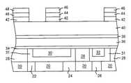
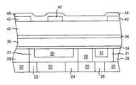
ここで、本発明の好ましい実施形態を説明するために、同じ参照数字が本発明の同じ特徴を指す、図1ないし図12を参照する。第一の実施形態においては、図1は、既存の銅相互接続部の配線層上に堆積された誘電体スタックを示す。既存の配線層は、タングステン・スタッド22、24、26を収容する基板誘電体層20を有し、その上にはTaN/Ta障壁層31内に銅線30、32を収容する誘電体層28が堆積されている。誘電体層は同じ組成であってもよいし、そうでなくてもよく、例えば、誘電体層20はリンシリケート・ガラス(PSG)であり、誘電体層28はドーピングされていないシリコン・ガラス(USG)、又は、シリコン、炭素、酸素、及び水素を含有するガラス(例えば、メソレート SiOx、SiCOH)であってよい。誘電体スタックは、底部から順に、例えば窒化シリコンSi3N4のようなキャップ層34、例えばUSG又はフッ素化シリコン・ガラス(FSG)のような良好な機械的特性及び熱伝導率を持つ絶縁体層36、例えばSiCのようなエッチング停止層38、例えばSiCOHのような良好な機械的特性及び熱伝導率を持つ誘電体(低k)材料の層40、及び、例えば炭化シリコンSiCのような第一ハードマスク層42で構成される。エッチング停止層38は、下方の絶縁層36に比べて高いエッチング速度比を有し、絶縁層40は該エッチング停止層38に比べて高いエッチング速度比を有する。次に、反射防止コーティング(ARC)層44及びレジスト層46が加えられ、図2に示すように、トレンチ・パターン開口部が像形成され、その後、ハードマスク層42がARC及びレジスト開口部を通してエッチングされる。次に、図3に示すように、例えば二酸化シリコンSiO2又はSi3N4のような第二ハードマスク層48が堆積される。その後バイア・レジスト層50が加えられ、図4に示すように、バイア・レジスト・パターン開口部を生成するように像形成される。次いで、図5に示すように、第二ハードマスク層48及びバイア開口部52、54がパターンの開口部を通してキャップ層34に至るまでエッチングされ、次いで、バイア・レジスト50が剥離される。To illustrate the preferred embodiment of the present invention, reference is now made to FIGS. 1-12, wherein like reference numerals refer to like features of the present invention. In a first embodiment, FIG. 1 shows a dielectric stack deposited on a wiring layer of an existing copper interconnect. The existing wiring layer has a substrate
図6は、ブランケット指向性除去エッチングが第一ハードマスク層42の上面より上方にある第二ハードマスク層48においてのみ行われる状態を示しており、これは、バイアの露光により露出される領域を除いて、該第一ハードマスク層42の縁の全域に隣接する該第二ハードマスク層スペーサ48a、48b、48cが残され、したがって、バイア52の側壁にはスペーサが形成されない状態を示す。その結果、スペーサ48a及び48bは自己整合してトレンチ/配線/バイア開口部56に隣接して配置され、スペーサ48cはバイア開口部54に隣接する。スペーサのサイズは、第一及び第二ハードマスク層のそれぞれの厚さによって決定される。次いで、バイア開口部52及び54を接合するトレンチ58が、エッチング停止層38に至るまでエッチッングされる。 FIG. 6 shows a state where the blanket directional removal etching is performed only in the second
次に、例えば、SiO2又はSi3N4のような第二絶縁体層60のコンフォーマルな堆積が、図7に示すように、既存構造の露出層上とバイア開口部52、54の中、及び、トレンチ56、58に加えられる。次いで、別のエッチングが、ハードマスク層42、48及びエッチング停止層38の上方の絶縁層60の部分のブランケット指向性除去のため、及び、バイア開口部52、54、トレンチ56の底部における絶縁体60の部分、並びに、バイア開口部52及び54の下方のキャップ層34の部分の除去のために実行される。このステップは、バイア開口部52、54及びトレンチ56、58をライニングする第二スペーサ60を残存させる。これらの第二スペーサは、トレンチ開口部56、58及びバイア開口部52、54の大きさを減少させているので、初めに形成するときには、トレンチ及びバイアの露光においては、スペーサ幅の約2倍だけ大きくエッチングするように露出する必要があることに注意すべきである。Next, a conformal deposition of a
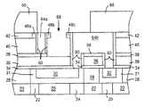
図9に示すように、トレンチ及びバイアが、初めに障壁(TaN/Taのような)及びシード層62により完全にライニングされ、次いで、銅64により充填され、その後、余分な材料が化学機械研磨法(CMP)によって除去されるように、通常の障壁・シード層法及び銅堆積法を用いてデュアル・ダマシン構造を充填する。銅の代わりに、アルミニウム、タングステン又は金などの他の導電材料を用いてもよい。図10は、エアーギャップ誘電体を受け取る領域だけを露出させるために用いるレジスト遮蔽マスク66を示す。層42、40及び38のSiC、SiCOH、SiCが露出された部分は、酸素プラズマへの露出、酸素反応性イオンエッチング(RIE)又は酸素注入によって劣化され、この後に、希釈HFエッチングが続き、図示のように、マスクされていない最小間隔の線64aと64bとの間に、張出し部48b、48cを持った空間68が形成される。例えば、超臨界CO2が、希釈HFの搬送媒体になり、酸素劣化膜を除去する。次いで、例えば、窒化シリコン又は窒化シリコン・カーボンのような絶縁性窒化物キャップ層70、及び、二酸化シリコン又はFSGの絶縁層72が加えられ、これらが、図11に示すように、エアーギャップ層68を完全に充填することなく閉鎖する。このように、エアーギャップ68は、相互接続層の上方で、キャップ層70を完全に貫通し、絶縁層72を部分的に通って延びる。エアーギャップ68の異質な充填物は、張出し部48bと48cとの間の開口部を最小にすることによって低減できる。或いは、表面張力特性のゆえに選ばれるスピン・オン型誘電体層を加えて、エアーギャップ68を充填されないままにしておくことができる。As shown in FIG. 9, the trenches and vias are first fully lined with a barrier (such as TaN / Ta) and
図11に示す半導体デバイスの構造においては、(先のトレンチ開口部56を充填する)相互接続ワイヤ64aは、(先のトレンチ58及びバイア開口部52、54を充填する)同じ相互接続層上の相互接続ワイヤ64bから間隔をおき、かつ、隣接している。スペーサ60b及び60cが、ワイヤ64aと64bとの間の隣接する側部に沿って形成され、エアーギャップ68の幅を減らして、実際のエアーギャップ誘電体幅が、ワイヤ64a、64bのプリントされた距離の間隔より小さくなるようにする。相互接続部64aと64bとの間に形成されたエアーギャップ誘電体68はまた、ワイヤの上面74a、74bより上方に、及び、ワイヤの下面76a、76bより下方に延びる。このように形成されたエアーギャップ68は、相互接続ワイヤ64a、64bの隣接する側部に自己整合する。 In the semiconductor device structure shown in FIG. 11, the
図12に完成型で示す別の実施形態は、窒化シリコンSi3N4キャップ層34及び70が、銅ワイヤ30、32、64a、64bの上で、自己整合型金属キャップ層34’及び70’と置き換えられたことを除いては、上述のものと同様なプロセスの順序を用いている。これは選択的金属堆積プロセスによって加えることができ、金属キャップ層は選択的タングステン又は選択的リン化コバルト・タングステン層を含むことができる。自己整合型金属キャップ層70’が用いられる場所では、絶縁層72が単独でエアーギャップ68の上部を封鎖する。Another embodiment, shown in complete form in FIG. 12, is that silicon nitride Si3 N4 cap layers 34 and 70 are self-aligned metal cap layers 34 ′ and 70 ′ over
このように、本発明は、自己整合型で調節可能なエアーギャップ誘電体を提供して、隣接し、かつ、緊密な間隔を持つ導電ワイヤ間又はバイア間の静電容量を低減する。隣接する銅線の上方及び下方のエアーギャップの高さは、フリンジ容量をなくし、構造の実効電気抵抗(k)が増加するように選択することができる。採用されるのに好ましいバイア誘電体は、比較的良好な機械的特性及び熱伝導率を持ったUSG又はFSGなどの酸化物である。犠牲トレンチ誘電体及びエッチング停止層を用いてエアーギャップを生成することができ、これらは、より高い熱伝導率及び機械的強度を持つ材料で作られていてよい。ブロックマスクを用いて、チップ上の、最小間隔で、低い静電容量を必要とする領域だけがエアーギャップを得るようすることができる。このことは、チップの熱伝導係数及び機械的安定性を最大にする。トレンチ及びバイアが酸化物又は窒化物スペーサによって定められるので、ライナー/障壁の先駆体が多孔性の低k誘電体に入り込むことに関する問題がなくなり、同様に、誘電体のCu汚染をもたらす障壁の完全性の問題、及び、Cuの抵抗率の増加をもたらす側壁の粗さの問題もなくなる。 Thus, the present invention provides a self-aligned and adjustable air gap dielectric to reduce the capacitance between adjacent and closely spaced conductive wires or vias. The height of the air gap above and below adjacent copper wires can be selected to eliminate the fringe capacitance and increase the effective electrical resistance (k) of the structure. Preferred via dielectrics to be employed are oxides such as USG or FSG with relatively good mechanical properties and thermal conductivity. Sacrificial trench dielectrics and etch stop layers can be used to create air gaps, which may be made of materials with higher thermal conductivity and mechanical strength. Using a block mask, only the areas on the chip that require low capacitance with minimal spacing can obtain an air gap. This maximizes the thermal conductivity coefficient and mechanical stability of the chip. Since the trenches and vias are defined by oxide or nitride spacers, there is no problem with liner / barrier precursors penetrating porous low-k dielectrics, as well as barrier integrity that leads to dielectric Cu contamination. And the problem of sidewall roughness which leads to an increase in Cu resistivity is also eliminated.
本発明は、特定の好ましい実施形態に関連して具体的に説明されているが、多くの代替的手法、修正及び変形が、前述の説明からみて、当業者にとって自明であろうことは明らかである。従って、添付の特許請求の範囲が、それらの代替的手法、修正及び変形を、本発明の真の範囲及び精神に入るものとして包含することが意図されている。 Although the invention has been described with particular reference to certain preferred embodiments, it is evident that many alternatives, modifications and variations will be apparent to those skilled in the art in view of the foregoing description. is there. Accordingly, the appended claims are intended to cover such alternatives, modifications and variations as fall within the true scope and spirit of this invention.
Claims (20)
Translated fromJapanese前記第一相互接続部及び前記第二相互接続部の隣接する側部に沿って形成されたスペーサと、
前記第一相互接続部と前記第二相互接続部との間に形成されたエアーギャップと、
を含み、前記エアーギャップが、前記第一相互接続部及び前記第二相互接続部の少なくとも一方の上面より上方で、かつ、前記第一相互接続部及び前記第二相互接続部の少なくとも一方の下面より下方に延び、前記スペーサ間の距離が前記エアーギャップの幅を定める、半導体デバイス。A first interconnect adjacent to the second interconnect on the interconnect layer;
Spacers formed along adjacent sides of the first interconnect and the second interconnect;
An air gap formed between the first interconnect and the second interconnect;
The air gap is above the upper surface of at least one of the first interconnect portion and the second interconnect portion, and the lower surface of at least one of the first interconnect portion and the second interconnect portion A semiconductor device that extends further downward and the distance between the spacers defines the width of the air gap.
半導体デバイスの複数の絶縁層を堆積するステップと、
第一ハードマスク絶縁層を前記複数の絶縁層上に堆積するステップと、
前記第一ハードマスク絶縁層の一部を除去して、相互接続部が形成されるべき離間した前記複数の絶縁層の最上部領域を露出させるステップと、
第二ハードマスク絶縁層を、前記第一ハードマスク絶縁層及び前記複数の絶縁層の最上部の露出領域の上に堆積するステップと、
前記第一ハードマスク絶縁層上の前記第二ハードマスク絶縁層の一部を除去して、相互接続部が形成されるべき複数の絶縁層の最上部領域を露出させ、前記相互接続部が形成されるべき前記複数の絶縁層の最上部領域に隣接して第二ハードマスク・スペーサは残すようにするステップと、
前記第一ハードマスク絶縁層及び前記第二ハードマスク・スペーサを用いて、下方の複数の絶縁層の少なくとも一つをエッチングして、相互接続部の開口部を形成するステップと、
コンフォーマル絶縁層を堆積して、前記相互接続部の開口部の側壁にスペーサを形成するステップと、
前記コンフォーマル絶縁層スペーサに隣接して導電性金属を堆積して、前記相互接続部の開口部に相互接続部を形成するステップと、
前記相互接続部と前記コンフォーマル絶縁層スペーサとの間の前記第一ハードマスク絶縁層及び前記下方の複数の絶縁層の一部をエッチングし、前記相互接続部及び前記コンフォーマル絶縁層スペーサに隣接して第二ハードマスク・スペーサを残すようにして、前記相互接続部の少なくとも一方の下方に延びるエアーギャップを形成するステップと、
少なくとも一つの絶縁層を、前記エアーギャップ上と、前記相互接続部及び前記コンフォーマル絶縁層スペーサ上に堆積して、前記エアーギャップを密閉するステップと、
を含む方法。A method of forming an air gap between a pair of interconnects on an interconnect layer in a semiconductor device,
Depositing a plurality of insulating layers of a semiconductor device;
Depositing a first hard mask insulating layer on the plurality of insulating layers;
Removing a portion of the first hard mask insulation layer to expose the top regions of the plurality of spaced apart insulation layers in which interconnects are to be formed;
Depositing a second hard mask insulating layer over the first hard mask insulating layer and an uppermost exposed region of the plurality of insulating layers;
A part of the second hard mask insulating layer on the first hard mask insulating layer is removed to expose the uppermost regions of the plurality of insulating layers where the interconnects are to be formed, thereby forming the interconnects Leaving a second hard mask spacer adjacent to a top region of the plurality of insulating layers to be done;
Etching at least one of the plurality of lower insulating layers using the first hard mask insulating layer and the second hard mask spacer to form an opening of the interconnect;
Depositing a conformal insulating layer to form spacers on the sidewalls of the interconnect openings;
Depositing a conductive metal adjacent to the conformal insulating layer spacer to form an interconnect in the opening of the interconnect; and
Etching a portion of the first hard mask insulating layer and the plurality of lower insulating layers between the interconnect and the conformal insulating layer spacer and adjacent to the interconnect and the conformal insulating layer spacer Forming an air gap extending below at least one of the interconnects, leaving a second hard mask spacer, and
Depositing at least one insulating layer on the air gap and on the interconnect and the conformal insulating layer spacer to seal the air gap;
Including methods.
前記第一ハードマスク絶縁層の一部を除去する前記ステップが、相互接続部が形成されるべき前記第四絶縁層の領域を露出させ、
前記相互接続部と前記コンフォーマル絶縁層スペーサとの間には、前記第一ハードマスク絶縁層と、前記第四絶縁層と、前記第三絶縁エッチング停止層とのエッチングされた部分があり、前記相互接続部及び前記コンフォーマル絶縁層スペーサに隣接して前記第二ハードマスク・スペーサを残すようにして、前記相互接続部の少なくとも一方の下方に延びる前記エアーギャップを形成する、
請求項17に記載の方法。Depositing a plurality of insulating layers of a semiconductor device, depositing a first insulating cap layer of the semiconductor device, depositing a second insulating layer on the first insulating cap layer, and a third insulating layer Depositing an etch stop layer on the second insulating layer; and depositing a fourth insulating layer on the third insulating etch stop layer;
The step of removing a portion of the first hard mask insulating layer exposes a region of the fourth insulating layer in which an interconnect is to be formed;
Between the interconnect portion and the conformal insulating layer spacer is an etched portion of the first hard mask insulating layer, the fourth insulating layer, and the third insulating etching stop layer, Forming the air gap extending below at least one of the interconnects, leaving the second hard mask spacer adjacent to the interconnect and the conformal insulating layer spacer;
The method of claim 17.
The at least one insulating layer on the interconnect includes a fifth insulating cap layer for the interconnect and a sixth insulating layer above the cap layer, and the air gap is the fifth insulating. 20. The method of claim 19, wherein the method extends completely through a cap layer and into a portion of the sixth insulating layer.
Applications Claiming Priority (3)
| Application Number | Priority Date | Filing Date | Title |
|---|---|---|---|
| US10/605,440 | 2003-09-30 | ||
| US10/605,440US7071532B2 (en) | 2003-09-30 | 2003-09-30 | Adjustable self-aligned air gap dielectric for low capacitance wiring |
| PCT/US2004/032404WO2005034200A2 (en) | 2003-09-30 | 2004-09-30 | Adjustable self-aligned air gap dielectric for low capacitance wiring |
Publications (2)
| Publication Number | Publication Date |
|---|---|
| JP2007507903Atrue JP2007507903A (en) | 2007-03-29 |
| JP5004585B2 JP5004585B2 (en) | 2012-08-22 |
Family
ID=34375676
Family Applications (1)
| Application Number | Title | Priority Date | Filing Date |
|---|---|---|---|
| JP2006534155AExpired - Fee RelatedJP5004585B2 (en) | 2003-09-30 | 2004-09-30 | Method for forming an air gap between a pair of interconnects on an interconnect layer in a semiconductor device |
Country Status (8)
| Country | Link |
|---|---|
| US (2) | US7071532B2 (en) |
| EP (1) | EP1668692B1 (en) |
| JP (1) | JP5004585B2 (en) |
| KR (1) | KR100800360B1 (en) |
| CN (1) | CN100466219C (en) |
| AT (1) | ATE547809T1 (en) |
| TW (1) | TWI319903B (en) |
| WO (1) | WO2005034200A2 (en) |
Families Citing this family (194)
| Publication number | Priority date | Publication date | Assignee | Title |
|---|---|---|---|---|
| KR100579846B1 (en)* | 2003-12-11 | 2006-05-12 | 동부일렉트로닉스 주식회사 | Metal wiring layer of semiconductor device and manufacturing method thereof |
| DE102004003337A1 (en)* | 2004-01-22 | 2005-08-18 | Infineon Technologies Ag | Plasma enhanced chemical vapor deposition method, silicon-oxygen-nitrogen containing material and layer assembly |
| KR20050114784A (en)* | 2004-06-01 | 2005-12-07 | 동부아남반도체 주식회사 | Method for forming cu interconnection of semiconductor device |
| DE102004050391B4 (en)* | 2004-10-15 | 2007-02-08 | Infineon Technologies Ag | Method for producing a layer arrangement and layer arrangement |
| KR100632653B1 (en)* | 2005-04-22 | 2006-10-12 | 주식회사 하이닉스반도체 | Bit line formation method of semiconductor device |
| US7629225B2 (en)* | 2005-06-13 | 2009-12-08 | Infineon Technologies Ag | Methods of manufacturing semiconductor devices and structures thereof |
| EP1744359A1 (en)* | 2005-07-12 | 2007-01-17 | ST Microelectronics Crolles 2 SAS | Interconnect structure having cavities in its dielectric portion |
| KR100672731B1 (en)* | 2005-10-04 | 2007-01-24 | 동부일렉트로닉스 주식회사 | Metal wiring formation method of semiconductor device |
| CN1996589B (en)* | 2005-12-31 | 2010-10-13 | 上海集成电路研发中心有限公司 | Structure of the Damascus using the gas filling to reduce the dielectric constant and its making method |
| EP2005468A1 (en) | 2006-03-30 | 2008-12-24 | Koninklijke Philips Electronics N.V. | Improving control of localized air gap formation in an interconnect stack |
| US7951723B2 (en)* | 2006-10-24 | 2011-05-31 | Taiwan Semiconductor Manufacturing Company, Ltd. | Integrated etch and supercritical CO2 process and chamber design |
| WO2008056295A1 (en)* | 2006-11-09 | 2008-05-15 | Nxp B.V. | A semiconductor device and a method of manufacturing thereof |
| US7973409B2 (en)* | 2007-01-22 | 2011-07-05 | International Business Machines Corporation | Hybrid interconnect structure for performance improvement and reliability enhancement |
| US20080185722A1 (en)* | 2007-02-05 | 2008-08-07 | Chung-Shi Liu | Formation process of interconnect structures with air-gaps and sidewall spacers |
| DE102007020269A1 (en)* | 2007-04-30 | 2008-11-06 | Advanced Micro Devices, Inc., Sunnyvale | Semiconductor structure with an electrical connection and method for its production |
| KR100854860B1 (en)* | 2007-06-27 | 2008-08-28 | 주식회사 하이닉스반도체 | Manufacturing Method of Memory Device |
| US20090072409A1 (en)* | 2007-09-14 | 2009-03-19 | International Business Machines Corporation | Interconnect Structures Incorporating Air-Gap Spacers |
| US20090075470A1 (en)* | 2007-09-14 | 2009-03-19 | International Business Machines Corporation | Method for Manufacturing Interconnect Structures Incorporating Air-Gap Spacers |
| US8476758B2 (en)* | 2008-01-09 | 2013-07-02 | International Business Machines Corporation | Airgap-containing interconnect structure with patternable low-k material and method of fabricating |
| US8108820B2 (en)* | 2008-09-11 | 2012-01-31 | International Business Machines Corporation | Enhanced conductivity in an airgapped integrated circuit |
| JP5491077B2 (en)* | 2009-06-08 | 2014-05-14 | キヤノン株式会社 | Semiconductor device and manufacturing method of semiconductor device |
| US8519540B2 (en)* | 2009-06-16 | 2013-08-27 | International Business Machines Corporation | Self-aligned dual damascene BEOL structures with patternable low- K material and methods of forming same |
| US8659115B2 (en)* | 2009-06-17 | 2014-02-25 | International Business Machines Corporation | Airgap-containing interconnect structure with improved patternable low-K material and method of fabricating |
| US8163658B2 (en)* | 2009-08-24 | 2012-04-24 | International Business Machines Corporation | Multiple patterning using improved patternable low-k dielectric materials |
| US8003516B2 (en)* | 2009-08-26 | 2011-08-23 | International Business Machines Corporation | BEOL interconnect structures and related fabrication methods |
| US7790601B1 (en)* | 2009-09-17 | 2010-09-07 | International Business Machines Corporation | Forming interconnects with air gaps |
| US8202783B2 (en) | 2009-09-29 | 2012-06-19 | International Business Machines Corporation | Patternable low-k dielectric interconnect structure with a graded cap layer and method of fabrication |
| US8637395B2 (en)* | 2009-11-16 | 2014-01-28 | International Business Machines Corporation | Methods for photo-patternable low-k (PPLK) integration with curing after pattern transfer |
| US8367540B2 (en)* | 2009-11-19 | 2013-02-05 | International Business Machines Corporation | Interconnect structure including a modified photoresist as a permanent interconnect dielectric and method of fabricating same |
| US8642252B2 (en) | 2010-03-10 | 2014-02-04 | International Business Machines Corporation | Methods for fabrication of an air gap-containing interconnect structure |
| US8896120B2 (en) | 2010-04-27 | 2014-11-25 | International Business Machines Corporation | Structures and methods for air gap integration |
| US8357609B2 (en)* | 2010-05-04 | 2013-01-22 | Globalfoundries Inc. | Dual damascene-like subtractive metal etch scheme |
| US8241992B2 (en) | 2010-05-10 | 2012-08-14 | International Business Machines Corporation | Method for air gap interconnect integration using photo-patternable low k material |
| US8373271B2 (en) | 2010-05-27 | 2013-02-12 | International Business Machines Corporation | Interconnect structure with an oxygen-doped SiC antireflective coating and method of fabrication |
| US9324576B2 (en) | 2010-05-27 | 2016-04-26 | Applied Materials, Inc. | Selective etch for silicon films |
| US8497203B2 (en) | 2010-08-13 | 2013-07-30 | International Business Machines Corporation | Semiconductor structures and methods of manufacture |
| US10283321B2 (en) | 2011-01-18 | 2019-05-07 | Applied Materials, Inc. | Semiconductor processing system and methods using capacitively coupled plasma |
| US8999856B2 (en) | 2011-03-14 | 2015-04-07 | Applied Materials, Inc. | Methods for etch of sin films |
| US9064815B2 (en) | 2011-03-14 | 2015-06-23 | Applied Materials, Inc. | Methods for etch of metal and metal-oxide films |
| US8890318B2 (en) | 2011-04-15 | 2014-11-18 | International Business Machines Corporation | Middle of line structures |
| US8900988B2 (en) | 2011-04-15 | 2014-12-02 | International Business Machines Corporation | Method for forming self-aligned airgap interconnect structures |
| US9054160B2 (en) | 2011-04-15 | 2015-06-09 | International Business Machines Corporation | Interconnect structure and method for fabricating on-chip interconnect structures by image reversal |
| US8822137B2 (en) | 2011-08-03 | 2014-09-02 | International Business Machines Corporation | Self-aligned fine pitch permanent on-chip interconnect structures and method of fabrication |
| US20130062732A1 (en) | 2011-09-08 | 2013-03-14 | International Business Machines Corporation | Interconnect structures with functional components and methods for fabrication |
| US8808563B2 (en) | 2011-10-07 | 2014-08-19 | Applied Materials, Inc. | Selective etch of silicon by way of metastable hydrogen termination |
| CN103137545B (en)* | 2011-11-25 | 2015-08-05 | 中芯国际集成电路制造(上海)有限公司 | Semiconductor device and forming method thereof |
| CN103165519B (en)* | 2011-12-08 | 2016-07-27 | 中芯国际集成电路制造(上海)有限公司 | A kind of manufacture method of semiconductor device |
| CN103178000B (en)* | 2011-12-20 | 2014-11-05 | 中芯国际集成电路制造(上海)有限公司 | Semiconductor device and forming method thereof |
| US9087753B2 (en) | 2012-05-10 | 2015-07-21 | International Business Machines Corporation | Printed transistor and fabrication method |
| US9267739B2 (en) | 2012-07-18 | 2016-02-23 | Applied Materials, Inc. | Pedestal with multi-zone temperature control and multiple purge capabilities |
| US9373517B2 (en) | 2012-08-02 | 2016-06-21 | Applied Materials, Inc. | Semiconductor processing with DC assisted RF power for improved control |
| KR101921465B1 (en) | 2012-08-22 | 2018-11-26 | 삼성전자 주식회사 | Semiconductor device and method for fabricating the same |
| US9034770B2 (en) | 2012-09-17 | 2015-05-19 | Applied Materials, Inc. | Differential silicon oxide etch |
| US9023734B2 (en) | 2012-09-18 | 2015-05-05 | Applied Materials, Inc. | Radical-component oxide etch |
| US9390937B2 (en) | 2012-09-20 | 2016-07-12 | Applied Materials, Inc. | Silicon-carbon-nitride selective etch |
| US9132436B2 (en) | 2012-09-21 | 2015-09-15 | Applied Materials, Inc. | Chemical control features in wafer process equipment |
| US8847401B2 (en) | 2012-10-31 | 2014-09-30 | International Business Machines Corporation | Semiconductor structure incorporating a contact sidewall spacer with a self-aligned airgap and a method of forming the semiconductor structure |
| US8969212B2 (en) | 2012-11-20 | 2015-03-03 | Applied Materials, Inc. | Dry-etch selectivity |
| US8980763B2 (en) | 2012-11-30 | 2015-03-17 | Applied Materials, Inc. | Dry-etch for selective tungsten removal |
| US9111877B2 (en) | 2012-12-18 | 2015-08-18 | Applied Materials, Inc. | Non-local plasma oxide etch |
| US8921234B2 (en) | 2012-12-21 | 2014-12-30 | Applied Materials, Inc. | Selective titanium nitride etching |
| US10256079B2 (en) | 2013-02-08 | 2019-04-09 | Applied Materials, Inc. | Semiconductor processing systems having multiple plasma configurations |
| US9362130B2 (en) | 2013-03-01 | 2016-06-07 | Applied Materials, Inc. | Enhanced etching processes using remote plasma sources |
| US9040422B2 (en) | 2013-03-05 | 2015-05-26 | Applied Materials, Inc. | Selective titanium nitride removal |
| US20140271097A1 (en) | 2013-03-15 | 2014-09-18 | Applied Materials, Inc. | Processing systems and methods for halide scavenging |
| US9493879B2 (en) | 2013-07-12 | 2016-11-15 | Applied Materials, Inc. | Selective sputtering for pattern transfer |
| US9773648B2 (en) | 2013-08-30 | 2017-09-26 | Applied Materials, Inc. | Dual discharge modes operation for remote plasma |
| US9576809B2 (en) | 2013-11-04 | 2017-02-21 | Applied Materials, Inc. | Etch suppression with germanium |
| US9520303B2 (en) | 2013-11-12 | 2016-12-13 | Applied Materials, Inc. | Aluminum selective etch |
| US9159671B2 (en) | 2013-11-19 | 2015-10-13 | International Business Machines Corporation | Copper wire and dielectric with air gaps |
| US9245762B2 (en) | 2013-12-02 | 2016-01-26 | Applied Materials, Inc. | Procedure for etch rate consistency |
| US9287095B2 (en) | 2013-12-17 | 2016-03-15 | Applied Materials, Inc. | Semiconductor system assemblies and methods of operation |
| US9287134B2 (en) | 2014-01-17 | 2016-03-15 | Applied Materials, Inc. | Titanium oxide etch |
| US9293568B2 (en) | 2014-01-27 | 2016-03-22 | Applied Materials, Inc. | Method of fin patterning |
| US9396989B2 (en) | 2014-01-27 | 2016-07-19 | Applied Materials, Inc. | Air gaps between copper lines |
| US9385028B2 (en) | 2014-02-03 | 2016-07-05 | Applied Materials, Inc. | Air gap process |
| US9499898B2 (en) | 2014-03-03 | 2016-11-22 | Applied Materials, Inc. | Layered thin film heater and method of fabrication |
| US9299575B2 (en) | 2014-03-17 | 2016-03-29 | Applied Materials, Inc. | Gas-phase tungsten etch |
| US9299537B2 (en) | 2014-03-20 | 2016-03-29 | Applied Materials, Inc. | Radial waveguide systems and methods for post-match control of microwaves |
| US9299538B2 (en) | 2014-03-20 | 2016-03-29 | Applied Materials, Inc. | Radial waveguide systems and methods for post-match control of microwaves |
| US9903020B2 (en) | 2014-03-31 | 2018-02-27 | Applied Materials, Inc. | Generation of compact alumina passivation layers on aluminum plasma equipment components |
| US9269590B2 (en) | 2014-04-07 | 2016-02-23 | Applied Materials, Inc. | Spacer formation |
| US9309598B2 (en) | 2014-05-28 | 2016-04-12 | Applied Materials, Inc. | Oxide and metal removal |
| US9406523B2 (en) | 2014-06-19 | 2016-08-02 | Applied Materials, Inc. | Highly selective doped oxide removal method |
| US9378969B2 (en) | 2014-06-19 | 2016-06-28 | Applied Materials, Inc. | Low temperature gas-phase carbon removal |
| US9425096B2 (en) | 2014-07-14 | 2016-08-23 | Qualcomm Incorporated | Air gap between tungsten metal lines for interconnects with reduced RC delay |
| US9425058B2 (en) | 2014-07-24 | 2016-08-23 | Applied Materials, Inc. | Simplified litho-etch-litho-etch process |
| US9496167B2 (en) | 2014-07-31 | 2016-11-15 | Applied Materials, Inc. | Integrated bit-line airgap formation and gate stack post clean |
| US9378978B2 (en) | 2014-07-31 | 2016-06-28 | Applied Materials, Inc. | Integrated oxide recess and floating gate fin trimming |
| US9159606B1 (en)* | 2014-07-31 | 2015-10-13 | Applied Materials, Inc. | Metal air gap |
| US9659753B2 (en) | 2014-08-07 | 2017-05-23 | Applied Materials, Inc. | Grooved insulator to reduce leakage current |
| US9553102B2 (en) | 2014-08-19 | 2017-01-24 | Applied Materials, Inc. | Tungsten separation |
| US9355856B2 (en) | 2014-09-12 | 2016-05-31 | Applied Materials, Inc. | V trench dry etch |
| US9368364B2 (en) | 2014-09-24 | 2016-06-14 | Applied Materials, Inc. | Silicon etch process with tunable selectivity to SiO2 and other materials |
| US9355862B2 (en) | 2014-09-24 | 2016-05-31 | Applied Materials, Inc. | Fluorine-based hardmask removal |
| US9613822B2 (en) | 2014-09-25 | 2017-04-04 | Applied Materials, Inc. | Oxide etch selectivity enhancement |
| US9966240B2 (en) | 2014-10-14 | 2018-05-08 | Applied Materials, Inc. | Systems and methods for internal surface conditioning assessment in plasma processing equipment |
| US9355922B2 (en) | 2014-10-14 | 2016-05-31 | Applied Materials, Inc. | Systems and methods for internal surface conditioning in plasma processing equipment |
| US9431294B2 (en)* | 2014-10-28 | 2016-08-30 | GlobalFoundries, Inc. | Methods of producing integrated circuits with an air gap |
| US11637002B2 (en) | 2014-11-26 | 2023-04-25 | Applied Materials, Inc. | Methods and systems to enhance process uniformity |
| US9299583B1 (en) | 2014-12-05 | 2016-03-29 | Applied Materials, Inc. | Aluminum oxide selective etch |
| US10573496B2 (en) | 2014-12-09 | 2020-02-25 | Applied Materials, Inc. | Direct outlet toroidal plasma source |
| US10224210B2 (en) | 2014-12-09 | 2019-03-05 | Applied Materials, Inc. | Plasma processing system with direct outlet toroidal plasma source |
| US9502258B2 (en) | 2014-12-23 | 2016-11-22 | Applied Materials, Inc. | Anisotropic gap etch |
| US9343272B1 (en) | 2015-01-08 | 2016-05-17 | Applied Materials, Inc. | Self-aligned process |
| US11257693B2 (en) | 2015-01-09 | 2022-02-22 | Applied Materials, Inc. | Methods and systems to improve pedestal temperature control |
| US9373522B1 (en) | 2015-01-22 | 2016-06-21 | Applied Mateials, Inc. | Titanium nitride removal |
| US9449846B2 (en) | 2015-01-28 | 2016-09-20 | Applied Materials, Inc. | Vertical gate separation |
| US9728437B2 (en) | 2015-02-03 | 2017-08-08 | Applied Materials, Inc. | High temperature chuck for plasma processing systems |
| US20160225652A1 (en) | 2015-02-03 | 2016-08-04 | Applied Materials, Inc. | Low temperature chuck for plasma processing systems |
| US9881805B2 (en) | 2015-03-02 | 2018-01-30 | Applied Materials, Inc. | Silicon selective removal |
| US9691645B2 (en) | 2015-08-06 | 2017-06-27 | Applied Materials, Inc. | Bolted wafer chuck thermal management systems and methods for wafer processing systems |
| US9741593B2 (en) | 2015-08-06 | 2017-08-22 | Applied Materials, Inc. | Thermal management systems and methods for wafer processing systems |
| US9349605B1 (en) | 2015-08-07 | 2016-05-24 | Applied Materials, Inc. | Oxide etch selectivity systems and methods |
| US10504700B2 (en) | 2015-08-27 | 2019-12-10 | Applied Materials, Inc. | Plasma etching systems and methods with secondary plasma injection |
| CN108369923B (en) | 2015-09-23 | 2023-03-14 | 英特尔公司 | Maskless air gap to prevent via punch-through |
| KR102334736B1 (en)* | 2015-12-03 | 2021-12-03 | 삼성전자주식회사 | Semiconductor device and method for manufacturing the semiconductor device |
| US9905463B2 (en) | 2015-12-15 | 2018-02-27 | International Business Machines Corporation | Self-aligned low dielectric constant gate cap and a method of forming the same |
| KR102616823B1 (en)* | 2015-12-16 | 2023-12-22 | 삼성전자주식회사 | Semiconductor Devices |
| US9349687B1 (en) | 2015-12-19 | 2016-05-24 | International Business Machines Corporation | Advanced manganese/manganese nitride cap/etch mask for air gap formation scheme in nanocopper low-K interconnect |
| US10504754B2 (en) | 2016-05-19 | 2019-12-10 | Applied Materials, Inc. | Systems and methods for improved semiconductor etching and component protection |
| US10522371B2 (en) | 2016-05-19 | 2019-12-31 | Applied Materials, Inc. | Systems and methods for improved semiconductor etching and component protection |
| US9865484B1 (en) | 2016-06-29 | 2018-01-09 | Applied Materials, Inc. | Selective etch using material modification and RF pulsing |
| US9859212B1 (en) | 2016-07-12 | 2018-01-02 | International Business Machines Corporation | Multi-level air gap formation in dual-damascene structure |
| US10032711B2 (en) | 2016-07-25 | 2018-07-24 | International Business Machines Corporation | Integrating metal-insulator-metal capacitors with air gap process flow |
| US10629473B2 (en) | 2016-09-09 | 2020-04-21 | Applied Materials, Inc. | Footing removal for nitride spacer |
| US10062575B2 (en) | 2016-09-09 | 2018-08-28 | Applied Materials, Inc. | Poly directional etch by oxidation |
| US9786553B1 (en) | 2016-09-16 | 2017-10-10 | International Business Machines Corporation | Advanced BEOL interconnect structure containing uniform air gaps |
| US10062585B2 (en) | 2016-10-04 | 2018-08-28 | Applied Materials, Inc. | Oxygen compatible plasma source |
| US9721789B1 (en) | 2016-10-04 | 2017-08-01 | Applied Materials, Inc. | Saving ion-damaged spacers |
| US9934942B1 (en) | 2016-10-04 | 2018-04-03 | Applied Materials, Inc. | Chamber with flow-through source |
| US10546729B2 (en) | 2016-10-04 | 2020-01-28 | Applied Materials, Inc. | Dual-channel showerhead with improved profile |
| US10062579B2 (en) | 2016-10-07 | 2018-08-28 | Applied Materials, Inc. | Selective SiN lateral recess |
| US9947549B1 (en) | 2016-10-10 | 2018-04-17 | Applied Materials, Inc. | Cobalt-containing material removal |
| US9768034B1 (en) | 2016-11-11 | 2017-09-19 | Applied Materials, Inc. | Removal methods for high aspect ratio structures |
| US10163696B2 (en) | 2016-11-11 | 2018-12-25 | Applied Materials, Inc. | Selective cobalt removal for bottom up gapfill |
| US10242908B2 (en) | 2016-11-14 | 2019-03-26 | Applied Materials, Inc. | Airgap formation with damage-free copper |
| US10026621B2 (en) | 2016-11-14 | 2018-07-17 | Applied Materials, Inc. | SiN spacer profile patterning |
| US10566206B2 (en) | 2016-12-27 | 2020-02-18 | Applied Materials, Inc. | Systems and methods for anisotropic material breakthrough |
| US10431429B2 (en) | 2017-02-03 | 2019-10-01 | Applied Materials, Inc. | Systems and methods for radial and azimuthal control of plasma uniformity |
| US10403507B2 (en) | 2017-02-03 | 2019-09-03 | Applied Materials, Inc. | Shaped etch profile with oxidation |
| US10043684B1 (en) | 2017-02-06 | 2018-08-07 | Applied Materials, Inc. | Self-limiting atomic thermal etching systems and methods |
| US10319739B2 (en) | 2017-02-08 | 2019-06-11 | Applied Materials, Inc. | Accommodating imperfectly aligned memory holes |
| US10943834B2 (en) | 2017-03-13 | 2021-03-09 | Applied Materials, Inc. | Replacement contact process |
| US9911652B1 (en) | 2017-03-29 | 2018-03-06 | International Business Machines Corporation | Forming self-aligned vias and air-gaps in semiconductor fabrication |
| US10319649B2 (en) | 2017-04-11 | 2019-06-11 | Applied Materials, Inc. | Optical emission spectroscopy (OES) for remote plasma monitoring |
| US11276590B2 (en) | 2017-05-17 | 2022-03-15 | Applied Materials, Inc. | Multi-zone semiconductor substrate supports |
| JP7176860B6 (en) | 2017-05-17 | 2022-12-16 | アプライド マテリアルズ インコーポレイテッド | Semiconductor processing chamber to improve precursor flow |
| US11276559B2 (en) | 2017-05-17 | 2022-03-15 | Applied Materials, Inc. | Semiconductor processing chamber for multiple precursor flow |
| US10497579B2 (en) | 2017-05-31 | 2019-12-03 | Applied Materials, Inc. | Water-free etching methods |
| US10049891B1 (en) | 2017-05-31 | 2018-08-14 | Applied Materials, Inc. | Selective in situ cobalt residue removal |
| US10920320B2 (en) | 2017-06-16 | 2021-02-16 | Applied Materials, Inc. | Plasma health determination in semiconductor substrate processing reactors |
| US10541246B2 (en) | 2017-06-26 | 2020-01-21 | Applied Materials, Inc. | 3D flash memory cells which discourage cross-cell electrical tunneling |
| US10727080B2 (en) | 2017-07-07 | 2020-07-28 | Applied Materials, Inc. | Tantalum-containing material removal |
| US10541184B2 (en) | 2017-07-11 | 2020-01-21 | Applied Materials, Inc. | Optical emission spectroscopic techniques for monitoring etching |
| US10354889B2 (en) | 2017-07-17 | 2019-07-16 | Applied Materials, Inc. | Non-halogen etching of silicon-containing materials |
| US10170336B1 (en) | 2017-08-04 | 2019-01-01 | Applied Materials, Inc. | Methods for anisotropic control of selective silicon removal |
| US10043674B1 (en) | 2017-08-04 | 2018-08-07 | Applied Materials, Inc. | Germanium etching systems and methods |
| US10297458B2 (en) | 2017-08-07 | 2019-05-21 | Applied Materials, Inc. | Process window widening using coated parts in plasma etch processes |
| US10629478B2 (en)* | 2017-08-22 | 2020-04-21 | International Business Machines Corporation | Dual-damascene formation with dielectric spacer and thin liner |
| US10128086B1 (en) | 2017-10-24 | 2018-11-13 | Applied Materials, Inc. | Silicon pretreatment for nitride removal |
| US10283324B1 (en) | 2017-10-24 | 2019-05-07 | Applied Materials, Inc. | Oxygen treatment for nitride etching |
| US10256112B1 (en) | 2017-12-08 | 2019-04-09 | Applied Materials, Inc. | Selective tungsten removal |
| US10903054B2 (en) | 2017-12-19 | 2021-01-26 | Applied Materials, Inc. | Multi-zone gas distribution systems and methods |
| US11328909B2 (en) | 2017-12-22 | 2022-05-10 | Applied Materials, Inc. | Chamber conditioning and removal processes |
| US10854426B2 (en) | 2018-01-08 | 2020-12-01 | Applied Materials, Inc. | Metal recess for semiconductor structures |
| US10679870B2 (en) | 2018-02-15 | 2020-06-09 | Applied Materials, Inc. | Semiconductor processing chamber multistage mixing apparatus |
| US10964512B2 (en) | 2018-02-15 | 2021-03-30 | Applied Materials, Inc. | Semiconductor processing chamber multistage mixing apparatus and methods |
| TWI766433B (en) | 2018-02-28 | 2022-06-01 | 美商應用材料股份有限公司 | Systems and methods to form airgaps |
| US10593560B2 (en) | 2018-03-01 | 2020-03-17 | Applied Materials, Inc. | Magnetic induction plasma source for semiconductor processes and equipment |
| US10319600B1 (en) | 2018-03-12 | 2019-06-11 | Applied Materials, Inc. | Thermal silicon etch |
| US10497573B2 (en) | 2018-03-13 | 2019-12-03 | Applied Materials, Inc. | Selective atomic layer etching of semiconductor materials |
| US10573527B2 (en) | 2018-04-06 | 2020-02-25 | Applied Materials, Inc. | Gas-phase selective etching systems and methods |
| US10490406B2 (en) | 2018-04-10 | 2019-11-26 | Appled Materials, Inc. | Systems and methods for material breakthrough |
| US10699879B2 (en) | 2018-04-17 | 2020-06-30 | Applied Materials, Inc. | Two piece electrode assembly with gap for plasma control |
| US10886137B2 (en) | 2018-04-30 | 2021-01-05 | Applied Materials, Inc. | Selective nitride removal |
| US10319629B1 (en)* | 2018-05-08 | 2019-06-11 | International Business Machines Corporation | Skip via for metal interconnects |
| US11469189B2 (en)* | 2018-06-29 | 2022-10-11 | Intel Corporation | Inductor and transmission line with air gap |
| US10872778B2 (en) | 2018-07-06 | 2020-12-22 | Applied Materials, Inc. | Systems and methods utilizing solid-phase etchants |
| US10755941B2 (en) | 2018-07-06 | 2020-08-25 | Applied Materials, Inc. | Self-limiting selective etching systems and methods |
| US10672642B2 (en) | 2018-07-24 | 2020-06-02 | Applied Materials, Inc. | Systems and methods for pedestal configuration |
| US10892198B2 (en) | 2018-09-14 | 2021-01-12 | Applied Materials, Inc. | Systems and methods for improved performance in semiconductor processing |
| US11049755B2 (en) | 2018-09-14 | 2021-06-29 | Applied Materials, Inc. | Semiconductor substrate supports with embedded RF shield |
| US11062887B2 (en) | 2018-09-17 | 2021-07-13 | Applied Materials, Inc. | High temperature RF heater pedestals |
| US11417534B2 (en) | 2018-09-21 | 2022-08-16 | Applied Materials, Inc. | Selective material removal |
| US11682560B2 (en) | 2018-10-11 | 2023-06-20 | Applied Materials, Inc. | Systems and methods for hafnium-containing film removal |
| US11121002B2 (en) | 2018-10-24 | 2021-09-14 | Applied Materials, Inc. | Systems and methods for etching metals and metal derivatives |
| US11437242B2 (en) | 2018-11-27 | 2022-09-06 | Applied Materials, Inc. | Selective removal of silicon-containing materials |
| US11721527B2 (en) | 2019-01-07 | 2023-08-08 | Applied Materials, Inc. | Processing chamber mixing systems |
| US10920319B2 (en) | 2019-01-11 | 2021-02-16 | Applied Materials, Inc. | Ceramic showerheads with conductive electrodes |
| CN112885773B (en)* | 2019-11-29 | 2024-10-22 | 长鑫存储技术有限公司 | Semiconductor structure and manufacturing method thereof |
| US11289371B2 (en) | 2020-01-23 | 2022-03-29 | International Business Machines Corporation | Top vias with selectively retained etch stops |
| US20210265205A1 (en)* | 2020-02-25 | 2021-08-26 | Tokyo Electron Limited | Dielectric etch stop layer for reactive ion etch (rie) lag reduction and chamfer corner protection |
| CN111501025B (en)* | 2020-04-23 | 2022-05-27 | 北京北方华创微电子装备有限公司 | Deposition apparatus |
Citations (4)
| Publication number | Priority date | Publication date | Assignee | Title |
|---|---|---|---|---|
| JPH11126820A (en)* | 1997-08-21 | 1999-05-11 | Matsushita Electron Corp | Semiconductor device and its manufacture |
| FR2784230A1 (en)* | 1998-10-05 | 2000-04-07 | St Microelectronics Sa | Air insulation formation between IC metallization level conductors, to produce intra- and inter-metal insulation comprises depositing and eliminating polycrystalline germanium to form air-filled interconnection spaces |
| JP2001110745A (en)* | 1999-10-13 | 2001-04-20 | Applied Materials Inc | Method for manufacturing semiconductor integrated circuit |
| US6413852B1 (en)* | 2000-08-31 | 2002-07-02 | International Business Machines Corporation | Method of forming multilevel interconnect structure containing air gaps including utilizing both sacrificial and placeholder material |
Family Cites Families (20)
| Publication number | Priority date | Publication date | Assignee | Title |
|---|---|---|---|---|
| US5117276A (en)* | 1989-08-14 | 1992-05-26 | Fairchild Camera And Instrument Corp. | High performance interconnect system for an integrated circuit |
| JPH0722583A (en)* | 1992-12-15 | 1995-01-24 | Internatl Business Mach Corp <Ibm> | Multilayer circuit device |
| US5324683A (en)* | 1993-06-02 | 1994-06-28 | Motorola, Inc. | Method of forming a semiconductor structure having an air region |
| US6281585B1 (en)* | 1997-06-30 | 2001-08-28 | Philips Electronics North America Corporation | Air gap dielectric in self-aligned via structures |
| US6184121B1 (en)* | 1997-07-10 | 2001-02-06 | International Business Machines Corporation | Chip interconnect wiring structure with low dielectric constant insulator and methods for fabricating the same |
| US6333255B1 (en)* | 1997-08-21 | 2001-12-25 | Matsushita Electronics Corporation | Method for making semiconductor device containing low carbon film for interconnect structures |
| US6242336B1 (en)* | 1997-11-06 | 2001-06-05 | Matsushita Electronics Corporation | Semiconductor device having multilevel interconnection structure and method for fabricating the same |
| US6211561B1 (en)* | 1998-11-16 | 2001-04-03 | Conexant Systems, Inc. | Interconnect structure and method employing air gaps between metal lines and between metal layers |
| US6150232A (en)* | 1999-02-05 | 2000-11-21 | Chartered Semiconductor Manufacturing Ltd. | Formation of low k dielectric |
| US6177329B1 (en)* | 1999-04-15 | 2001-01-23 | Kurt Pang | Integrated circuit structures having gas pockets and method for forming integrated circuit structures having gas pockets |
| US6211057B1 (en)* | 1999-09-03 | 2001-04-03 | Taiwan Semiconductor Manufacturing Company | Method for manufacturing arch air gap in multilevel interconnection |
| US6200900B1 (en)* | 1999-10-08 | 2001-03-13 | National Semiconductor Corporation | Method for formation of an air gap in an integrated circuit architecture |
| KR20010063852A (en)* | 1999-12-24 | 2001-07-09 | 박종섭 | A method for forming a self aligned contact of semiconductor device |
| US6815329B2 (en)* | 2000-02-08 | 2004-11-09 | International Business Machines Corporation | Multilayer interconnect structure containing air gaps and method for making |
| US6329279B1 (en)* | 2000-03-20 | 2001-12-11 | United Microelectronics Corp. | Method of fabricating metal interconnect structure having outer air spacer |
| US6423629B1 (en)* | 2000-05-31 | 2002-07-23 | Kie Y. Ahn | Multilevel copper interconnects with low-k dielectrics and air gaps |
| US6472266B1 (en)* | 2001-06-18 | 2002-10-29 | Taiwan Semiconductor Manufacturing Company | Method to reduce bit line capacitance in cub drams |
| DE10140754A1 (en) | 2001-08-20 | 2003-03-27 | Infineon Technologies Ag | Circuit arrangement and method for manufacturing a circuit arrangement |
| US7138329B2 (en)* | 2002-11-15 | 2006-11-21 | United Microelectronics Corporation | Air gap for tungsten/aluminum plug applications |
| US6838354B2 (en)* | 2002-12-20 | 2005-01-04 | Freescale Semiconductor, Inc. | Method for forming a passivation layer for air gap formation |
- 2003
- 2003-09-30USUS10/605,440patent/US7071532B2/ennot_activeExpired - Lifetime
- 2004
- 2004-09-20TWTW093128432Apatent/TWI319903B/ennot_activeIP Right Cessation
- 2004-09-30ATAT04809842Tpatent/ATE547809T1/enactive
- 2004-09-30KRKR1020067004177Apatent/KR100800360B1/ennot_activeExpired - Fee Related
- 2004-09-30WOPCT/US2004/032404patent/WO2005034200A2/enactiveApplication Filing
- 2004-09-30CNCNB2004800274275Apatent/CN100466219C/ennot_activeExpired - Fee Related
- 2004-09-30EPEP04809842Apatent/EP1668692B1/ennot_activeExpired - Lifetime
- 2004-09-30JPJP2006534155Apatent/JP5004585B2/ennot_activeExpired - Fee Related
- 2006
- 2006-05-05USUS11/418,921patent/US7358148B2/ennot_activeExpired - Fee Related
Patent Citations (5)
| Publication number | Priority date | Publication date | Assignee | Title |
|---|---|---|---|---|
| JPH11126820A (en)* | 1997-08-21 | 1999-05-11 | Matsushita Electron Corp | Semiconductor device and its manufacture |
| FR2784230A1 (en)* | 1998-10-05 | 2000-04-07 | St Microelectronics Sa | Air insulation formation between IC metallization level conductors, to produce intra- and inter-metal insulation comprises depositing and eliminating polycrystalline germanium to form air-filled interconnection spaces |
| JP2001110745A (en)* | 1999-10-13 | 2001-04-20 | Applied Materials Inc | Method for manufacturing semiconductor integrated circuit |
| US6413852B1 (en)* | 2000-08-31 | 2002-07-02 | International Business Machines Corporation | Method of forming multilevel interconnect structure containing air gaps including utilizing both sacrificial and placeholder material |
| US20020127844A1 (en)* | 2000-08-31 | 2002-09-12 | International Business Machines Corporation | Multilevel interconnect structure containing air gaps and method for making |
Also Published As
| Publication number | Publication date |
|---|---|
| WO2005034200A2 (en) | 2005-04-14 |
| US20050067673A1 (en) | 2005-03-31 |
| CN1856872A (en) | 2006-11-01 |
| US7071532B2 (en) | 2006-07-04 |
| US20060202302A1 (en) | 2006-09-14 |
| TW200520154A (en) | 2005-06-16 |
| KR20060072129A (en) | 2006-06-27 |
| EP1668692B1 (en) | 2012-02-29 |
| ATE547809T1 (en) | 2012-03-15 |
| KR100800360B1 (en) | 2008-02-04 |
| JP5004585B2 (en) | 2012-08-22 |
| EP1668692A2 (en) | 2006-06-14 |
| TWI319903B (en) | 2010-01-21 |
| US7358148B2 (en) | 2008-04-15 |
| CN100466219C (en) | 2009-03-04 |
| EP1668692A4 (en) | 2007-05-09 |
| WO2005034200A3 (en) | 2005-09-29 |
Similar Documents
| Publication | Publication Date | Title |
|---|---|---|
| JP5004585B2 (en) | Method for forming an air gap between a pair of interconnects on an interconnect layer in a semiconductor device | |
| US7037851B2 (en) | Methods for selective integration of airgaps and devices made by such methods | |
| US7078352B2 (en) | Methods for selective integration of airgaps and devices made by such methods | |
| US8383507B2 (en) | Method for fabricating air gap interconnect structures | |
| US6984577B1 (en) | Damascene interconnect structure and fabrication method having air gaps between metal lines and metal layers | |
| US20040232552A1 (en) | Air gap dual damascene process and structure | |
| CN100392853C (en) | Non-porous metal interconnect structure and method of forming same | |
| US20070120263A1 (en) | Conductor track arrangement and associated production method | |
| JP2009194286A (en) | Semiconductor device and manufacturing method thereof | |
| JP2003309173A (en) | Semiconductor device and manufacturing method thereof | |
| JP2006019480A (en) | Method for manufacturing semiconductor apparatus | |
| JP2010171072A (en) | Semiconductor device and process of fabricating the same | |
| JPH11317446A (en) | Semiconductor device and manufacturing method thereof | |
| CN119650518B (en) | Method for preparing semiconductor structure and semiconductor structure | |
| JP3887175B2 (en) | Semiconductor device and manufacturing method thereof | |
| JP4878434B2 (en) | Semiconductor device and manufacturing method thereof | |
| US20070194405A1 (en) | Dielectric material with reduced dielectric constant and methods of manufacturing the same | |
| JP4086811B2 (en) | Method for forming a porous organic dielectric layer | |
| CN113707602B (en) | Method for forming semiconductor structure and semiconductor structure | |
| JP2005129937A (en) | Low K integrated circuit interconnection structure | |
| JP2024523801A (en) | Subtractive metal etch for improved back-end interconnect and cross-point isolation | |
| JP4383262B2 (en) | Semiconductor device and manufacturing method thereof | |
| US20010048162A1 (en) | Semiconductor device having a structure of a multilayer interconnection unit and manufacturing method thereof | |
| TWI381444B (en) | Method for fabricating an opening | |
| JP4967207B2 (en) | Manufacturing method of semiconductor device |
Legal Events
| Date | Code | Title | Description |
|---|---|---|---|
| A621 | Written request for application examination | Free format text:JAPANESE INTERMEDIATE CODE: A621 Effective date:20070816 | |
| A977 | Report on retrieval | Free format text:JAPANESE INTERMEDIATE CODE: A971007 Effective date:20100805 | |
| A131 | Notification of reasons for refusal | Free format text:JAPANESE INTERMEDIATE CODE: A131 Effective date:20110906 | |
| A521 | Request for written amendment filed | Free format text:JAPANESE INTERMEDIATE CODE: A523 Effective date:20111121 | |
| A131 | Notification of reasons for refusal | Free format text:JAPANESE INTERMEDIATE CODE: A131 Effective date:20120104 | |
| A521 | Request for written amendment filed | Free format text:JAPANESE INTERMEDIATE CODE: A523 Effective date:20120329 | |
| TRDD | Decision of grant or rejection written | ||
| A01 | Written decision to grant a patent or to grant a registration (utility model) | Free format text:JAPANESE INTERMEDIATE CODE: A01 Effective date:20120424 | |
| A01 | Written decision to grant a patent or to grant a registration (utility model) | Free format text:JAPANESE INTERMEDIATE CODE: A01 | |
| A61 | First payment of annual fees (during grant procedure) | Free format text:JAPANESE INTERMEDIATE CODE: A61 Effective date:20120522 | |
| FPAY | Renewal fee payment (event date is renewal date of database) | Free format text:PAYMENT UNTIL: 20150601 Year of fee payment:3 | |
| R150 | Certificate of patent or registration of utility model | Ref document number:5004585 Country of ref document:JP Free format text:JAPANESE INTERMEDIATE CODE: R150 Free format text:JAPANESE INTERMEDIATE CODE: R150 | |
| R250 | Receipt of annual fees | Free format text:JAPANESE INTERMEDIATE CODE: R250 | |
| R250 | Receipt of annual fees | Free format text:JAPANESE INTERMEDIATE CODE: R250 | |
| R250 | Receipt of annual fees | Free format text:JAPANESE INTERMEDIATE CODE: R250 | |
| LAPS | Cancellation because of no payment of annual fees |