JP2007311558A - Vapor growth apparatus and method for manufacturing vapor growth substrate - Google Patents
Vapor growth apparatus and method for manufacturing vapor growth substrateDownload PDFInfo
- Publication number
- JP2007311558A JP2007311558AJP2006139229AJP2006139229AJP2007311558AJP 2007311558 AJP2007311558 AJP 2007311558AJP 2006139229 AJP2006139229 AJP 2006139229AJP 2006139229 AJP2006139229 AJP 2006139229AJP 2007311558 AJP2007311558 AJP 2007311558A
- Authority
- JP
- Japan
- Prior art keywords
- semiconductor substrate
- vapor phase
- phase growth
- susceptor
- source gas
- Prior art date
- Legal status (The legal status is an assumption and is not a legal conclusion. Google has not performed a legal analysis and makes no representation as to the accuracy of the status listed.)
- Abandoned
Links
Images


Classifications
- C—CHEMISTRY; METALLURGY
- C23—COATING METALLIC MATERIAL; COATING MATERIAL WITH METALLIC MATERIAL; CHEMICAL SURFACE TREATMENT; DIFFUSION TREATMENT OF METALLIC MATERIAL; COATING BY VACUUM EVAPORATION, BY SPUTTERING, BY ION IMPLANTATION OR BY CHEMICAL VAPOUR DEPOSITION, IN GENERAL; INHIBITING CORROSION OF METALLIC MATERIAL OR INCRUSTATION IN GENERAL
- C23C—COATING METALLIC MATERIAL; COATING MATERIAL WITH METALLIC MATERIAL; SURFACE TREATMENT OF METALLIC MATERIAL BY DIFFUSION INTO THE SURFACE, BY CHEMICAL CONVERSION OR SUBSTITUTION; COATING BY VACUUM EVAPORATION, BY SPUTTERING, BY ION IMPLANTATION OR BY CHEMICAL VAPOUR DEPOSITION, IN GENERAL
- C23C16/00—Chemical coating by decomposition of gaseous compounds, without leaving reaction products of surface material in the coating, i.e. chemical vapour deposition [CVD] processes
- C23C16/44—Chemical coating by decomposition of gaseous compounds, without leaving reaction products of surface material in the coating, i.e. chemical vapour deposition [CVD] processes characterised by the method of coating
- C23C16/458—Chemical coating by decomposition of gaseous compounds, without leaving reaction products of surface material in the coating, i.e. chemical vapour deposition [CVD] processes characterised by the method of coating characterised by the method used for supporting substrates in the reaction chamber
- C23C16/4582—Rigid and flat substrates, e.g. plates or discs
- C23C16/4583—Rigid and flat substrates, e.g. plates or discs the substrate being supported substantially horizontally
- C23C16/4584—Rigid and flat substrates, e.g. plates or discs the substrate being supported substantially horizontally the substrate being rotated
- C—CHEMISTRY; METALLURGY
- C30—CRYSTAL GROWTH
- C30B—SINGLE-CRYSTAL GROWTH; UNIDIRECTIONAL SOLIDIFICATION OF EUTECTIC MATERIAL OR UNIDIRECTIONAL DEMIXING OF EUTECTOID MATERIAL; REFINING BY ZONE-MELTING OF MATERIAL; PRODUCTION OF A HOMOGENEOUS POLYCRYSTALLINE MATERIAL WITH DEFINED STRUCTURE; SINGLE CRYSTALS OR HOMOGENEOUS POLYCRYSTALLINE MATERIAL WITH DEFINED STRUCTURE; AFTER-TREATMENT OF SINGLE CRYSTALS OR A HOMOGENEOUS POLYCRYSTALLINE MATERIAL WITH DEFINED STRUCTURE; APPARATUS THEREFOR
- C30B23/00—Single-crystal growth by condensing evaporated or sublimed materials
- C30B23/02—Epitaxial-layer growth
- C—CHEMISTRY; METALLURGY
- C30—CRYSTAL GROWTH
- C30B—SINGLE-CRYSTAL GROWTH; UNIDIRECTIONAL SOLIDIFICATION OF EUTECTIC MATERIAL OR UNIDIRECTIONAL DEMIXING OF EUTECTOID MATERIAL; REFINING BY ZONE-MELTING OF MATERIAL; PRODUCTION OF A HOMOGENEOUS POLYCRYSTALLINE MATERIAL WITH DEFINED STRUCTURE; SINGLE CRYSTALS OR HOMOGENEOUS POLYCRYSTALLINE MATERIAL WITH DEFINED STRUCTURE; AFTER-TREATMENT OF SINGLE CRYSTALS OR A HOMOGENEOUS POLYCRYSTALLINE MATERIAL WITH DEFINED STRUCTURE; APPARATUS THEREFOR
- C30B25/00—Single-crystal growth by chemical reaction of reactive gases, e.g. chemical vapour-deposition growth
- C30B25/02—Epitaxial-layer growth
Landscapes
- Chemical & Material Sciences (AREA)
- Engineering & Computer Science (AREA)
- Materials Engineering (AREA)
- Metallurgy (AREA)
- Organic Chemistry (AREA)
- Crystallography & Structural Chemistry (AREA)
- General Chemical & Material Sciences (AREA)
- Chemical Kinetics & Catalysis (AREA)
- Mechanical Engineering (AREA)
- Chemical Vapour Deposition (AREA)
Abstract
Translated fromJapaneseDescription
Translated fromJapanese本発明は、気相成長装置および気相成長基板の製造方法に関する。 The present invention relates to a vapor phase growth apparatus and a method for manufacturing a vapor phase growth substrate.
半導体発光素子および半導体レーザ素子などの光半導体装置は化学気相成長装置、例えばMOCVD(Metal Organic Chemical Vapor Deposition)装置を用いてクラッド層や発光層などの材質の異なった複数の半導体薄膜を順次成長させることにより製造される。 Optical semiconductor devices such as semiconductor light-emitting elements and semiconductor laser elements are grown using a chemical vapor deposition apparatus, such as a MOCVD (Metal Organic Chemical Vapor Deposition) apparatus, to sequentially grow multiple semiconductor thin films of different materials such as cladding layers and light-emitting layers. Manufactured.
従来、結晶成長面を下側にして半導体基板をサセプタ上に配置するフェースダウン方式の気相成長装置が知られている(例えば、特許文献1または特許文献2参照。)。 Conventionally, there is known a face-down type vapor phase growth apparatus in which a semiconductor substrate is disposed on a susceptor with a crystal growth surface facing down (see, for example, Patent Document 1 or Patent Document 2).
特許文献1に開示された気相成長装置は、半導体基板の結晶成長面を下向きにして保持するとともに、半導体基板を公転させながら自転させている。これにより、半導体基板の温度均一性や薄膜の膜厚均一性を向上させている。 The vapor phase growth apparatus disclosed in Patent Document 1 holds the semiconductor substrate with its crystal growth surface facing downward and rotates the semiconductor substrate while revolving. Thereby, the temperature uniformity of the semiconductor substrate and the film thickness uniformity of the thin film are improved.
しかしながら、特許文献1に開示された気相成長装置は、反応生成物が部材上に堆積すると半導体基板の結晶成長面との間に生じる段差に起因して、半導体基板の外周部に結晶欠陥が発生するという問題がある。 However, the vapor phase growth apparatus disclosed in Patent Document 1 has crystal defects in the outer peripheral portion of the semiconductor substrate due to a step generated between the crystal growth surface of the semiconductor substrate when the reaction product is deposited on the member. There is a problem that occurs.
その結果、半導体基板の外周部の結晶欠陥を防止するために、反応生成物が堆積した部材を定期的に交換しなければならないという問題がある。 As a result, there is a problem that the member on which the reaction product is deposited must be periodically replaced in order to prevent crystal defects on the outer peripheral portion of the semiconductor substrate.
特許文献2に開示された気相成長装置は、回転する板状のサセプタに、複数の半導体基板を周方向に配し、且つ成長面をガス流路側に向けて支持し、サセプタの直径方向に原料ガスを流し、半導体基板の結晶成長面を原料ガスの流れ方向に対して傾けて設置している。 In the vapor phase growth apparatus disclosed in
半導体基板の結晶成長面を原料ガスの流れ方向に対して平行にセットすると、上流側から供給された原料ガスはそのほとんどがサセプタより上流側で分解してしまう。
しかし、半導体基板を傾けることにより、上流側では原料ガスが半導体基板の結晶成長面に当たりにくくなるため、成長する半導体薄膜の膜厚が減少し、上流側での原料の消費が減少する。
下流側では原料ガスが半導体基板の結晶成長面に当たりやすくなるとともに、上流側での原料の消費が減少して未分解の原料ガスが多く供給されるようになるので、成長する半導体薄膜の膜厚が厚くなる。これにより、半導体薄膜の膜厚の面内均一性を向上させている。If the crystal growth surface of the semiconductor substrate is set parallel to the flow direction of the source gas, most of the source gas supplied from the upstream side is decomposed upstream from the susceptor.
However, tilting the semiconductor substrate makes it difficult for the source gas to hit the crystal growth surface of the semiconductor substrate on the upstream side, thereby reducing the thickness of the growing semiconductor thin film and reducing the consumption of the source on the upstream side.
Since the source gas tends to hit the crystal growth surface of the semiconductor substrate on the downstream side, the consumption of the source material on the upstream side is reduced and more undecomposed source gas is supplied, so the film thickness of the growing semiconductor thin film Becomes thicker. Thereby, the in-plane uniformity of the film thickness of the semiconductor thin film is improved.
然しながら、特許文献2に開示された気相成長装置は、半導体薄膜の膜厚均一性向上のために半導体基板を傾けるものであり、半導体基板が公転しながら自転している場合には半導体基板を傾ける必要は生じない。また、サセプタやホルダなどの部材上に堆積する反応生成物の影響については何ら開示していない。
本発明は、反応生成物の堆積による部材交換頻度が低い気相成長装置および気相成長基板の製造方法を提供する。 The present invention provides a vapor phase growth apparatus and a method for producing a vapor phase growth substrate with a low frequency of member replacement due to deposition of reaction products.
本発明の一態様の気相成長装置は、容器と、前記容器に収納された半導体基板をフェースダウンで原料ガスの流れ方向に対して傾けて周方向に配設するとともに、前記半導体基板を公転可能に保持する保持手段と、前記半導体基板を結晶成長面と反対側から加熱する加熱手段と、前記半導体基板に前記原料ガスを前記保持手段の公転中心部から外周部に向かって放射状に供給するガス供給手段とを具備することを特徴としている。 A vapor phase growth apparatus according to an embodiment of the present invention includes a container and a semiconductor substrate housed in the container that are disposed face-down in a circumferential direction with respect to the flow direction of the source gas, and the semiconductor substrate is revolved. Holding means for holding the substrate, heating means for heating the semiconductor substrate from the side opposite to the crystal growth surface, and supplying the source gas to the semiconductor substrate in a radial manner from the center of revolution of the holding means toward the outer periphery. And a gas supply means.
また、本発明の一態様の気相成長基板の成長方法は、容器内に複数の半導体基板をフェースダウンで原料ガスの流れ方向に対して傾けて収納する工程と、前記半導体基板を公転させながら所定の温度に加熱し、前記原料ガスを前記公転中心部から外周部に向かって放射状に供給して、前記半導体基板上に半導体膜を形成する工程とを具備することを特徴としている。 The method for growing a vapor phase growth substrate according to one embodiment of the present invention includes a step of housing a plurality of semiconductor substrates in a container in a tilted manner with respect to a flow direction of a source gas in a container, and revolving the semiconductor substrates. Heating to a predetermined temperature, and supplying the source gas radially from the revolution center portion toward the outer peripheral portion to form a semiconductor film on the semiconductor substrate.
本発明によれば、反応生成物の堆積による部材交換頻度が低い気相成長装置および気相成長基板の製造方法が得られる。 ADVANTAGE OF THE INVENTION According to this invention, the manufacturing method of the vapor phase growth apparatus and vapor phase growth board | substrate with low member replacement frequency by deposition of a reaction product are obtained.
以下、本発明の実施例について図面を参照しながら説明する。 Embodiments of the present invention will be described below with reference to the drawings.
本発明の実施例1に係る気相成長装置について図1乃至図5を用いて説明する。図1は本実施例の気相成長装置の構成を示す断面図、図2はサセプタを示す図で、図2(a)はその平面図、図2(b)は図2(a)のA−A線に沿って切断し矢印方向に眺めた断面図、図3はホルダを示す図で、図3(a)はその平面図、図3(b)は図3(a)のB−B線に沿って切断し矢印方向に眺めた断面図である。 A vapor phase growth apparatus according to Embodiment 1 of the present invention will be described with reference to FIGS. FIG. 1 is a cross-sectional view showing the configuration of the vapor phase growth apparatus of the present embodiment, FIG. 2 is a view showing a susceptor, FIG. 2 (a) is a plan view thereof, and FIG. 2 (b) is A in FIG. Sectional view cut along line A and viewed in the direction of the arrow, FIG. 3 is a view showing the holder, FIG. 3A is a plan view thereof, and FIG. 3B is BB of FIG. It is sectional drawing which cut | disconnected along the line and looked at the arrow direction.
図4は外周リングを示す図で、図4(a)はその平面図、図4(b)は図4(a)のC−C線に沿って切断し矢印方向に眺めた断面図、図5は傾斜して公転しながら自転する半導体基板を示す図で、図5(a)はその平面図、図5(b)は図5(a)のD−D線に沿って切断し矢印方向に眺めた断面図である。 FIG. 4 is a view showing the outer ring, FIG. 4 (a) is a plan view thereof, FIG. 4 (b) is a cross-sectional view taken along the line CC of FIG. 5 is a view showing a semiconductor substrate that rotates while revolving with inclination, FIG. 5A is a plan view thereof, and FIG. 5B is a cross-sectional view taken along the line DD in FIG. 5A. FIG.
図1に示すように、本実施例の気相成長装置10は内部を減圧可能に構成された容器11と、容器11に収納された複数の半導体基板12をフェースダウンで原料ガスの流れ27a、27b方向に対して傾けて周方向に配設するとともに、半導体基板12をそれぞれ自転および公転可能に保持するためのホルダ13、サセプタ14、外周リング15(保持手段)と、半導体基板12を結晶成長面と反対側から加熱するヒータ16(加熱手段)と、原料ガスを半導体基板12にサセプタ14の中心部から外周部に向かって放射状に供給するノズル17(ガス供給手段)と、を具備している。 As shown in FIG. 1, a vapor
容器11は、半導体基板12上に半導体薄膜を形成するための処理室であり、例えば水冷ジャケット構造のステンレス製容器で、底部にガス流入口18と、底部の両側にガス排気口19a、19bと、サセプタ14を回転して半導体基板12を公転させる回転軸20を保持し、容器11内部の気密を維持するための気密シール部(図示せず)が設けられている。 The container 11 is a processing chamber for forming a semiconductor thin film on the
ガス流入口18は、配管21を介して半導体薄膜を形成するための原料ガスを供給するガス制御装置22に連通されている。
ガス排気口19a、19bはガス排気管(図示せず)を介して排気装置(図示せず)に連通されている。排気されたガスは除害装置(図示せず)により処理された後に、大気中に排出される。The
The
ヒータ16は、例えば炭化珪素(SiC)で被覆されたリング状のカーボン製ヒータで、サセプタ14の上方に半導体基板12の裏面と対向するように配置されている。
ヒータ16の上方に配置された熱遮蔽板23は、ヒータ16の熱が直接容器11の天板を加熱するのを防止するとともに、サセプタ14側へ熱を反射させて半導体基板12の加熱効率を高めるように機能している。The
The
半導体基板12の温度は、ヒータ16に設けられたほぞ状の孔(図示せず)に絶縁部材(図示せず)を介して嵌入された熱電対16aにより間接的にモニターされる。
熱電対が検出したヒータ16の温度は、温度調節器24に入力される。温度調節器24は、熱電対16aの検出した温度と温度目標値とが等しくなるようにサイリスタ25を駆動してヒータ16の加熱電力を制御している。
従って、半導体基板12の温度は、ヒータ16の温度を適正に変更することにより制御される。The temperature of the
The temperature of the
Therefore, the temperature of the
ノズル17から放出されたガスは、サセプタ14とガス整流板26との間をサセプタ14の中心部から外周部に向かって放射状に流れ、層状のガス流れ27a、27bを生成する。 The gas released from the
回転軸20は、例えばステンレス製のシャフトで、下部に連結された回転手段(図示せず)によりサセプタ14を水平方向に回転し、半導体基板12を公転させている。
ガス整流板26は回転軸20に取り付けられており、サセプタ14と連動して回転している。The rotating
The
外周リング15は、サセプタ14の外周に同軸的に配置され、筒状の支持部28上に固定されている。 The outer
ホルダ13の外周部側面には歯車状の第1溝(図示せず)が形成され、外周リング15の内周側面には歯車状の第1溝と歯合する歯車状の第2溝(図示せず)が形成されている。 A gear-shaped first groove (not shown) is formed on the outer peripheral side surface of the
サセプタ14が回転すると、ホルダ13が歯車状の第1および第2溝の歯合により回転し、半導体基板12を自転させることができる。
ホルダ13の第1溝の歯数と外周リング15の第2溝の歯数との比が1:nの場合に、サセプタ14が1回転する間に、ホルダ13がn回転する。When the
When the ratio between the number of teeth of the first groove of the
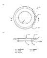
具体的には、図2に示すように、サセプタ14は、例えば炭化珪素(SiC)が被覆されたカーボン材で、外周部14aが中央部14bに対して所定の角度θ傾いた傘状をしており、外周部14aと中央部14bとの境には段差14cが形成されている。 Specifically, as shown in FIG. 2, the
サセプタ14の外周部14aには、ホルダ13を装着するための複数の第1貫通孔40が周方向に配設されている。 A plurality of first through
図3に示すように、ホルダ13は、例えば炭化珪素(SiC)が被覆されたカーボン材で、内側面がテーパ状の第2貫通孔41が形成された筒状の胴部42と、側面に歯車状の第1溝43が形成された鍔状の外周部44と、胴部42の下面に内部に向かって僅かに突出した爪45を有している。 As shown in FIG. 3, the
半導体基板12は、ホルダ13の第2貫通孔41内に収納され、爪45で保持されている。ホルダ13の胴部42はサセプタ14の第1貫通孔40に嵌合し、半導体基板12の結晶成長面がサセプタ14の外周部14aの傾斜面と一致するように位置している。 The
図4に示すように、外周リング15は、例えば炭化珪素(SiC)が被覆された炭素材で、内周側面に歯車状の第1溝と歯合する歯車状の第2溝46が形成されたリングで、サセプタ14の周りに同軸的に配置されている。 As shown in FIG. 4, the outer
これにより、図5に示すように、ホルダ13、サセプタ14、外周リング15を有する保持手段により、半導体基板12を原料ガス流れ27a、27b方向に対して傾けて、自転および公転させることが可能である。 As a result, as shown in FIG. 5, the holding means having the
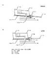
図6は気相成長中の半導体基板12の外周部におけるガス流れを従来例と比較して示す図で、図6(a)が本実施例の場合、図6(b)が従来例の場合である。 FIG. 6 is a diagram showing the gas flow in the outer peripheral portion of the
従来例の場合を先に説明する。図6(b)に示すように、気相成長によりホルダ52およびサセプタ53の原料ガス流れ側の面上に反応生成物54a、54bが堆積し、基板12とホルダ52上に堆積した反応生成物54aとの間に段差55が形成される。段差55は、気相成長を繰り返すにつれ反応生成物54aが蓄積されて大きくなる。 The case of the conventional example will be described first. As shown in FIG. 6B,
段差55が大きくなるにつれ、段差55が障害となり原料ガス流れに乱れが生じ、半導体基板12の外周部に十分到達することができなくなる。 As the
その結果、半導体基板12の外周部では、原料ガスの組成が変化し、半導体基板12の外周部に所謂ハッチと呼ばれる結晶欠陥が発生する。 As a result, the composition of the source gas changes in the outer peripheral portion of the
一方、図6(a)に示すように、本実施例でも気相成長によりホルダ13およびサセプタ14の原料ガス流れ側の面上に反応生成物50a、50bが堆積し、基板12とホルダ13上に堆積した反応生成物50aとの間に段差51が形成されることは同様である。 On the other hand, as shown in FIG. 6A, also in this embodiment,
しかし、半導体基板12が原料ガス流れ方向に対して角度θだけ傾斜しているので、その分、原料ガス流れの乱れが抑えられ、原料ガスは半導体基板12の外周部に到達しやすくなる。 However, since the
その結果、半導体基板12の外周部における原料ガスの組成の変化が抑制され、半導体基板12の外周部に所謂ハッチと呼ばれる結晶欠陥の発生を防止することができる。 As a result, a change in the composition of the source gas at the outer peripheral portion of the
図7は得られた気相成長基板を従来例と比較して示す図で、図7(a)が本実施例の場合、図7(b)が従来例の場合である。 FIG. 7 is a view showing the obtained vapor phase growth substrate in comparison with the conventional example. FIG. 7A shows the case of this embodiment, and FIG. 7B shows the case of the conventional example.
図7(a)に示すように、本実施例では外周部に結晶欠陥のない気相成長基板60が得られる。
一方、図7(b)に示すように、従来例では外周部に、幅Wが3mm程度の、所謂ハッチと呼ばれる結晶欠陥61を有する気相成長基板62が得られる。As shown in FIG. 7A, in this embodiment, a vapor
On the other hand, as shown in FIG. 7B, in the conventional example, a vapor
図8は反応性生物が堆積したホルダおよびサセプタの交換頻度を従来例と比較して示す図である。 FIG. 8 is a diagram showing the exchange frequency of the holder and susceptor on which reactive organisms are deposited in comparison with the conventional example.
図8に示すように、実験によれば、従来例では、段差55が300μm程度になると半導体基板12の外周全体に幅3mm程度の結晶欠陥の発生がみられるようになった。
従って、1回の気相成長における反応生成物54a、54bの厚さが、例えば3μm程度なので、気相成長を10回繰り返すと段差54が300μm程度に達し、ホルダ52、サセプタ53の交換が必要になる。As shown in FIG. 8, according to the experiment, in the conventional example, when the
Accordingly, the thickness of the
一方、本実施例では半導体基板12を、例えば10°程度傾けた場合に、段差51が600μm程度になるまでは、半導体基板12に結晶欠陥の発生がみられなかった。
従って、1回の気相成長における反応生成物50a、50bの厚さが、例えば3μm程度なので、気相成長を20回繰り返し段差51が600μm程度に達したときに、ホルダ13、サセプタ14を交換すればよい。On the other hand, in this example, when the
Therefore, since the thickness of the
従って、本実施例は従来例に比べて、反応生成物が堆積したホルダ13、サセプタ14の交換頻度を減らすことが可能である。 Therefore, in the present embodiment, the replacement frequency of the
図9は本実施例の気相成長装置10を用いた気相成長基板70の製造工程を示すフローチャート、図10は気相成長基板70およびそれを用いた光半導体装置84の構造を示す断面図である。
本実施例は、GaAs基板上にInGaAlP系の発光層を含む半導体薄膜を成長し、可視発光ダイオードを製造する場合の例である。FIG. 9 is a flowchart showing a manufacturing process of the vapor
In this embodiment, a visible light emitting diode is manufactured by growing a semiconductor thin film including an InGaAlP light emitting layer on a GaAs substrate.
図9に示すように、はじめに容器11内に半導体基板12をガス流れ方向に対して10°傾いたサセプタ14に基板を載せたホルダ13をセットし(ステップS01)、サセプタ14を回転させ、半導体基板12を、例えば10rpmで公転させながら50rpmで自転させる(ステップS02)。 As shown in FIG. 9, first, a
次に、キャリアガスとして水素ガスとGaAs基板からAsの揮発を抑制するためにアルシン(AsH3)ガスを流しながら、ヒータ16により半導体基板12を半導体薄膜の成長温度に加熱する(ステップS03)。 Next, the
次に、原料ガスとして、III族ガスのトリメチルガリウム(TMG)、トリメチルアルミニウム(TMA)、トリメチルインジウム(TMI)、V族ガスのアルシン、フォスヒン(PH3)、p型ドーパントガスのジメチル亜鉛(DMZ)、n型ドーパントガスのシラン(SiH4)を適宜流しながら、GaAs基板上にGaAsバッファ層からキャップ層までを順次成長させる(ステップS04)。 Next, as source gases, group III gas trimethylgallium (TMG), trimethylaluminum (TMA), trimethylindium (TMI), group V gas arsine, phosphine (PH3), p-type dopant gas dimethylzinc (DMZ) Then, the GaAs buffer layer to the cap layer are sequentially grown on the GaAs substrate while appropriately flowing n-type dopant gas silane (SiH4) (step S04).
即ち、図10(a)に示すように、n−GaAs基板71上に、n−GaAsバッファ層72と、n−InAlPとn−InGaAlPを交互に積層した光反射層73と、n−InAlPクラッド層74と、InGaPとInGaAlPを交互に積層したMQW(Multiple Quantum Well)活性層75と、p―InAlPクラッド層76と、p―GaAlAs電流拡散層77と、p―InGaAlP耐湿層78と、p―GaAsコンタクト層79と、n―InGaAlP電流ブロック層80と、InGaAlPキャップ層81を順次積層して気相成長基板70を形成する。 That is, as shown in FIG. 10A, on an n-GaAs substrate 71, an n-
次に、気相成長基板70を冷却して、容器11から気相成長基板70を取り出し(ステップ05)、同一ホルダ13およびサセプタ14を使用して所定回数、例えば20回気相成長を行なったかをチェックする。
所定回数に達していない場合に、ステップS01へ戻り、同一ホルダ13およびサセプタ14を使用して気相成長を繰り返す。
一方、所定回数に達した場合に、ホルダ13およびサセプタ14を反応生成物が堆積していないホルダ13およびサセプタ14と交換する。Next, the vapor
If the predetermined number of times has not been reached, the process returns to step S01, and vapor phase growth is repeated using the
On the other hand, when the predetermined number of times is reached, the
次に、更に気相成長を続けるか否かがチェックされ、気相成長を続ける場合に、交換したホルダ13およびサセプタ14を使用して気相成長を繰り返す。一方、気相成長を続けない場合に、気相成長基板70の製造を終了する。 Next, whether or not to continue the vapor phase growth is checked, and when the vapor phase growth is continued, the vapor phase growth is repeated using the replaced
次に、図10(b)に示すように、得られた気相成長基板70にp側電極82およびn側電極83が形成され、光半導体装置84が製造される。
即ち、気相成長基板70のキャップ層81をエッチングにより除去し、中央部にのみ電流ブロック層80を残置して電流ブロック層80をエッチングにより除去した後、コンタクト層79上にp側電極82を形成し、p側電極82が形成されていないコンタクト層79をエッチングにより除去する。また、n−GaAs基板71の裏面にはn側電極83を形成する。Next, as shown in FIG. 10B, the p-
That is, the cap layer 81 of the vapor
次に、p側電極82およびn側電極83が形成された気相成長基板70をダイサーによりダイシングして、個々のチップに分割することにより、例えばサイズが300μm角の光半導体装置84が得られる。 Next, the vapor
図11は気相成長基板70の膜厚分布を従来例1および従来例2と比較して示す図で、図11(a)が本実施例の場合、図11(b)が従来例1の場合、図11(c)が従来例2の場合である。 FIG. 11 is a view showing the film thickness distribution of the vapor
図11に示すように、本実施例は、半導体基板12が原料ガスの流れ方向に対して傾斜していても半導体基板12を公転させながら自転させているので、膜厚均一性を損なうこと無く、従来例1および従来例2と同様に膜厚均一性の高い半導体薄膜を成長させることができる。 As shown in FIG. 11, in this embodiment, even when the
以上説明したように、本実施例の気相成長装置10は、半導体基板12をフェースダウンで原料ガスの流れ方向に対して傾けるとともに、半導体基板12を公転させながら自転させている。 As described above, the vapor
その結果、ホルダ13およびサセプタ14上に堆積した反応性生物と半導体基板12の結晶成長面との間の段差51による原料ガスの流れの乱れが抑制され、半導体基板12の外周部に結晶欠陥61が生じるのを遅延させることができる。
従って、反応生成物が堆積した部材の交換頻度を低くすることができ、稼働率の高い気相成長装置10が得られる。As a result, the disturbance of the flow of the source gas due to the
Therefore, the replacement frequency of the member on which the reaction product is deposited can be reduced, and the vapor
ここでは、半導体基板12の傾斜角度θが10°の場合について説明したが、一般に5°乃至15°程度が適当である。 Here, the case where the inclination angle θ of the
図12は本発明の実施例2に係る気相成長装置90の構成の要部を示す断面図である。本実施例において、上記実施例1と同一の構成部分には同一符号を付してその説明は省略し、異なる部分についてのみ説明する。 FIG. 12 is a cross-sectional view showing the main part of the configuration of the vapor
本実施例が実施例1と異なる点は、半導体基板の結晶成長面に対向するガス整流板が半導体基板側に傾斜していることにある。 This embodiment differs from the first embodiment in that the gas rectifying plate facing the crystal growth surface of the semiconductor substrate is inclined toward the semiconductor substrate.
即ち、図12に示すように、本実施例の気相成長装置90は、外周部91aが中央部91bに対して角度θ2だけ半導体基板12側に傾斜したガス整流板91を具備している。 That is, as shown in FIG. 12, the vapor
外周部91aが傾斜したガス整流板91により、原料ガスの下流側の流路が狭くなり、原料ガスは半導体基板12の結晶成長面に向かうので、半導体基板12の傾斜角度θを実質的に大きくしたことになる。
即ち、基板半導体基板12の傾斜角度θは、近似的にサセプタ14の外周部14aの傾斜角度θ1とガス整流板91の外周部91aの傾斜角度θ2の和で表わすことができる。The
That is, the inclination angle θ of the
その結果、半導体基板12の外周部に対する原料ガス流れの乱れを更に抑制することが可能である。 As a result, it is possible to further suppress the disturbance of the raw material gas flow with respect to the outer peripheral portion of the
以上説明したように、本実施例に係る気相成長装置90は、外周部91aが傾斜したガス整流板91を具備している。その結果、半導体基板12の傾斜角度θを実質的に大きくすることができる利点がある。 As described above, the vapor
従って、半導体基板12の目的の傾斜角度θを得るのに、ガス整流板91の外周部91aの傾斜角度θ2を大きくして、サセプタ14の外周部14aの傾斜角度θ1を小さくすることもできる。 Therefore, in order to obtain the target tilt angle θ of the
10、90 気相成長装置
11 容器
12 半導体基板
13、52 ホルダ
14、53 サセプタ
14a、44、91a 外周部
14b、91b 中央部
14c、51、55 段差
15 外周リング
16 ヒータ
16a 熱電対
17 ノズル
18 ガス流入口
19a、19b ガス排気口
20 回転軸
21 配管
22ガス制御装置
23 熱遮蔽板
24 温度調節器
25 サイリスタ
26、91 ガス整流板
27a、27b ガス流れ
28 支持部
40 第1貫通孔
41 第2貫通孔
42 胴部
43 第1溝
45 爪
46 第2溝
50a、50b、54a、54b 反応生成物
70 気相成長基板
82 p側電極
83 n側電極
84 光半導体装置
10, 90 Vapor growth apparatus 11
Claims (5)
Translated fromJapanese前記容器に収納された半導体基板をフェースダウンで原料ガスの流れ方向に対して傾けて周方向に配設するとともに、前記半導体基板を公転可能に保持する保持手段と、
前記半導体基板を結晶成長面と反対側から加熱する加熱手段と、
前記半導体基板に前記原料ガスを前記保持手段の公転中心部から外周部に向かって放射状に供給するガス供給手段と、
を具備することを特徴とする気相成長装置。A container,
The semiconductor substrate housed in the container is disposed in the circumferential direction inclined face-down with respect to the flow direction of the source gas, and holding means for holding the semiconductor substrate in a revolving manner,
Heating means for heating the semiconductor substrate from the side opposite to the crystal growth surface;
Gas supply means for supplying the source gas to the semiconductor substrate radially from the revolution center portion of the holding means toward the outer periphery;
A vapor phase growth apparatus comprising:
中央部に対して所定の角度傾いた傾斜面を有する外周部に第1貫通孔が周方向に配設された傘状のサセプタと、
前記第1貫通孔に嵌合し、鍔状の外周部側面に歯車状の第1溝が形成され、内部にすり鉢状の第2貫通孔が形成され、前記半導体基板を前記第2貫通孔内に収納するホルダと、
内周側面に前記歯車状の第1溝と歯合する歯車状の第2溝が形成され、前記サセプタの外周に同軸的に配置された外周リングと、
を具備することを特徴とする請求項2に記載の気相成長装置。The holding means is
An umbrella-shaped susceptor in which a first through hole is disposed in a circumferential direction on an outer peripheral portion having an inclined surface inclined at a predetermined angle with respect to a central portion;
A gear-shaped first groove is formed on a side surface of the bowl-shaped outer peripheral portion, fitted into the first through-hole, and a mortar-shaped second through-hole is formed therein, and the semiconductor substrate is placed in the second through-hole. A holder for storing in,
A gear-shaped second groove that meshes with the gear-shaped first groove is formed on an inner peripheral side surface, and an outer peripheral ring disposed coaxially on the outer periphery of the susceptor;
The vapor phase growth apparatus according to claim 2, comprising:
前記半導体基板を公転させながら所定の温度に加熱し、前記原料ガスを前記公転中心部から外周部に向かって放射状に供給して、前記半導体基板上に半導体膜を形成する工程と、
を具備することを特徴とする気相成長基板の製造方法。Storing a plurality of semiconductor substrates in a container inclined face-down with respect to the flow direction of the source gas;
Heating the semiconductor substrate to a predetermined temperature while revolving, supplying the source gas radially from the revolution center to the outer periphery, and forming a semiconductor film on the semiconductor substrate;
A method for producing a vapor phase growth substrate, comprising:
Priority Applications (3)
| Application Number | Priority Date | Filing Date | Title |
|---|---|---|---|
| JP2006139229AJP2007311558A (en) | 2006-05-18 | 2006-05-18 | Vapor growth apparatus and method for manufacturing vapor growth substrate |
| TW096114053ATW200746269A (en) | 2006-05-18 | 2007-04-20 | Vapor phase growth apparatus and method for vapor phase growth |
| US11/750,589US20070266932A1 (en) | 2006-05-18 | 2007-05-18 | Vapor phase growth apparatus and method for vapor phase growth |
Applications Claiming Priority (1)
| Application Number | Priority Date | Filing Date | Title |
|---|---|---|---|
| JP2006139229AJP2007311558A (en) | 2006-05-18 | 2006-05-18 | Vapor growth apparatus and method for manufacturing vapor growth substrate |
Publications (1)
| Publication Number | Publication Date |
|---|---|
| JP2007311558Atrue JP2007311558A (en) | 2007-11-29 |
Family
ID=38710835
Family Applications (1)
| Application Number | Title | Priority Date | Filing Date |
|---|---|---|---|
| JP2006139229AAbandonedJP2007311558A (en) | 2006-05-18 | 2006-05-18 | Vapor growth apparatus and method for manufacturing vapor growth substrate |
Country Status (3)
| Country | Link |
|---|---|
| US (1) | US20070266932A1 (en) |
| JP (1) | JP2007311558A (en) |
| TW (1) | TW200746269A (en) |
Cited By (1)
| Publication number | Priority date | Publication date | Assignee | Title |
|---|---|---|---|---|
| TWI468637B (en)* | 2010-12-06 | 2015-01-11 | Beijing Nmc Co Ltd | A hot plate and a substrate processing apparatus to which the hot plate is applied |
Families Citing this family (298)
| Publication number | Priority date | Publication date | Assignee | Title |
|---|---|---|---|---|
| JP4379585B2 (en)* | 2003-12-17 | 2009-12-09 | 信越半導体株式会社 | Vapor phase growth apparatus and epitaxial wafer manufacturing method |
| KR101486377B1 (en)* | 2007-08-31 | 2015-01-26 | 엘지전자 주식회사 | METHOD AND APPARATUS FOR SUPPORTING POST-BROWSING IN MOBILE USE OF DIGITAL CONTENT |
| US9394608B2 (en) | 2009-04-06 | 2016-07-19 | Asm America, Inc. | Semiconductor processing reactor and components thereof |
| JP5341706B2 (en) | 2009-10-16 | 2013-11-13 | 株式会社ニューフレアテクノロジー | Semiconductor manufacturing apparatus and semiconductor manufacturing method |
| US20130023129A1 (en) | 2011-07-20 | 2013-01-24 | Asm America, Inc. | Pressure transmitter for a semiconductor processing environment |
| US10714315B2 (en) | 2012-10-12 | 2020-07-14 | Asm Ip Holdings B.V. | Semiconductor reaction chamber showerhead |
| DE102012110836A1 (en)* | 2012-11-12 | 2014-02-27 | Osram Opto Semiconductors Gmbh | Optoelectronic semiconductor chip and method for producing optoelectronic semiconductor chips |
| US20160376700A1 (en) | 2013-02-01 | 2016-12-29 | Asm Ip Holding B.V. | System for treatment of deposition reactor |
| CN105164309B (en)* | 2013-05-01 | 2019-04-12 | 应用材料公司 | Injection and Vent Design for Controlling Epitaxy Chamber Flow |
| DE102013114203A1 (en)* | 2013-12-17 | 2015-06-18 | Osram Opto Semiconductors Gmbh | Wafer carrier, reactor and method for temperature measurement |
| US11015245B2 (en) | 2014-03-19 | 2021-05-25 | Asm Ip Holding B.V. | Gas-phase reactor and system having exhaust plenum and components thereof |
| US10858737B2 (en) | 2014-07-28 | 2020-12-08 | Asm Ip Holding B.V. | Showerhead assembly and components thereof |
| US10941490B2 (en) | 2014-10-07 | 2021-03-09 | Asm Ip Holding B.V. | Multiple temperature range susceptor, assembly, reactor and system including the susceptor, and methods of using the same |
| US10276355B2 (en) | 2015-03-12 | 2019-04-30 | Asm Ip Holding B.V. | Multi-zone reactor, system including the reactor, and method of using the same |
| US10458018B2 (en) | 2015-06-26 | 2019-10-29 | Asm Ip Holding B.V. | Structures including metal carbide material, devices including the structures, and methods of forming same |
| US10211308B2 (en) | 2015-10-21 | 2019-02-19 | Asm Ip Holding B.V. | NbMC layers |
| US11139308B2 (en) | 2015-12-29 | 2021-10-05 | Asm Ip Holding B.V. | Atomic layer deposition of III-V compounds to form V-NAND devices |
| US10529554B2 (en) | 2016-02-19 | 2020-01-07 | Asm Ip Holding B.V. | Method for forming silicon nitride film selectively on sidewalls or flat surfaces of trenches |
| US10343920B2 (en) | 2016-03-18 | 2019-07-09 | Asm Ip Holding B.V. | Aligned carbon nanotubes |
| US10190213B2 (en) | 2016-04-21 | 2019-01-29 | Asm Ip Holding B.V. | Deposition of metal borides |
| US10367080B2 (en) | 2016-05-02 | 2019-07-30 | Asm Ip Holding B.V. | Method of forming a germanium oxynitride film |
| US11453943B2 (en) | 2016-05-25 | 2022-09-27 | Asm Ip Holding B.V. | Method for forming carbon-containing silicon/metal oxide or nitride film by ALD using silicon precursor and hydrocarbon precursor |
| US10612137B2 (en) | 2016-07-08 | 2020-04-07 | Asm Ip Holdings B.V. | Organic reactants for atomic layer deposition |
| US9859151B1 (en) | 2016-07-08 | 2018-01-02 | Asm Ip Holding B.V. | Selective film deposition method to form air gaps |
| KR102532607B1 (en) | 2016-07-28 | 2023-05-15 | 에이에스엠 아이피 홀딩 비.브이. | Substrate processing apparatus and method of operating the same |
| US9887082B1 (en) | 2016-07-28 | 2018-02-06 | Asm Ip Holding B.V. | Method and apparatus for filling a gap |
| US9812320B1 (en) | 2016-07-28 | 2017-11-07 | Asm Ip Holding B.V. | Method and apparatus for filling a gap |
| US10643826B2 (en) | 2016-10-26 | 2020-05-05 | Asm Ip Holdings B.V. | Methods for thermally calibrating reaction chambers |
| US11532757B2 (en) | 2016-10-27 | 2022-12-20 | Asm Ip Holding B.V. | Deposition of charge trapping layers |
| US10714350B2 (en) | 2016-11-01 | 2020-07-14 | ASM IP Holdings, B.V. | Methods for forming a transition metal niobium nitride film on a substrate by atomic layer deposition and related semiconductor device structures |
| KR102546317B1 (en) | 2016-11-15 | 2023-06-21 | 에이에스엠 아이피 홀딩 비.브이. | Gas supply unit and substrate processing apparatus including the same |
| KR102762543B1 (en) | 2016-12-14 | 2025-02-05 | 에이에스엠 아이피 홀딩 비.브이. | Substrate processing apparatus |
| US11447861B2 (en) | 2016-12-15 | 2022-09-20 | Asm Ip Holding B.V. | Sequential infiltration synthesis apparatus and a method of forming a patterned structure |
| US11581186B2 (en) | 2016-12-15 | 2023-02-14 | Asm Ip Holding B.V. | Sequential infiltration synthesis apparatus |
| KR102700194B1 (en) | 2016-12-19 | 2024-08-28 | 에이에스엠 아이피 홀딩 비.브이. | Substrate processing apparatus |
| US10269558B2 (en) | 2016-12-22 | 2019-04-23 | Asm Ip Holding B.V. | Method of forming a structure on a substrate |
| US10867788B2 (en) | 2016-12-28 | 2020-12-15 | Asm Ip Holding B.V. | Method of forming a structure on a substrate |
| US11390950B2 (en) | 2017-01-10 | 2022-07-19 | Asm Ip Holding B.V. | Reactor system and method to reduce residue buildup during a film deposition process |
| US10468261B2 (en) | 2017-02-15 | 2019-11-05 | Asm Ip Holding B.V. | Methods for forming a metallic film on a substrate by cyclical deposition and related semiconductor device structures |
| US10529563B2 (en) | 2017-03-29 | 2020-01-07 | Asm Ip Holdings B.V. | Method for forming doped metal oxide films on a substrate by cyclical deposition and related semiconductor device structures |
| KR102457289B1 (en) | 2017-04-25 | 2022-10-21 | 에이에스엠 아이피 홀딩 비.브이. | Method for depositing a thin film and manufacturing a semiconductor device |
| US10892156B2 (en) | 2017-05-08 | 2021-01-12 | Asm Ip Holding B.V. | Methods for forming a silicon nitride film on a substrate and related semiconductor device structures |
| US10770286B2 (en) | 2017-05-08 | 2020-09-08 | Asm Ip Holdings B.V. | Methods for selectively forming a silicon nitride film on a substrate and related semiconductor device structures |
| US10886123B2 (en) | 2017-06-02 | 2021-01-05 | Asm Ip Holding B.V. | Methods for forming low temperature semiconductor layers and related semiconductor device structures |
| US12040200B2 (en) | 2017-06-20 | 2024-07-16 | Asm Ip Holding B.V. | Semiconductor processing apparatus and methods for calibrating a semiconductor processing apparatus |
| US11306395B2 (en) | 2017-06-28 | 2022-04-19 | Asm Ip Holding B.V. | Methods for depositing a transition metal nitride film on a substrate by atomic layer deposition and related deposition apparatus |
| KR20190009245A (en) | 2017-07-18 | 2019-01-28 | 에이에스엠 아이피 홀딩 비.브이. | Methods for forming a semiconductor device structure and related semiconductor device structures |
| US11374112B2 (en)* | 2017-07-19 | 2022-06-28 | Asm Ip Holding B.V. | Method for depositing a group IV semiconductor and related semiconductor device structures |
| US10541333B2 (en) | 2017-07-19 | 2020-01-21 | Asm Ip Holding B.V. | Method for depositing a group IV semiconductor and related semiconductor device structures |
| US11018002B2 (en) | 2017-07-19 | 2021-05-25 | Asm Ip Holding B.V. | Method for selectively depositing a Group IV semiconductor and related semiconductor device structures |
| US10590535B2 (en) | 2017-07-26 | 2020-03-17 | Asm Ip Holdings B.V. | Chemical treatment, deposition and/or infiltration apparatus and method for using the same |
| TWI815813B (en) | 2017-08-04 | 2023-09-21 | 荷蘭商Asm智慧財產控股公司 | Showerhead assembly for distributing a gas within a reaction chamber |
| US10770336B2 (en) | 2017-08-08 | 2020-09-08 | Asm Ip Holding B.V. | Substrate lift mechanism and reactor including same |
| US10692741B2 (en) | 2017-08-08 | 2020-06-23 | Asm Ip Holdings B.V. | Radiation shield |
| US11769682B2 (en) | 2017-08-09 | 2023-09-26 | Asm Ip Holding B.V. | Storage apparatus for storing cassettes for substrates and processing apparatus equipped therewith |
| US11139191B2 (en) | 2017-08-09 | 2021-10-05 | Asm Ip Holding B.V. | Storage apparatus for storing cassettes for substrates and processing apparatus equipped therewith |
| US11830730B2 (en) | 2017-08-29 | 2023-11-28 | Asm Ip Holding B.V. | Layer forming method and apparatus |
| KR102491945B1 (en) | 2017-08-30 | 2023-01-26 | 에이에스엠 아이피 홀딩 비.브이. | Substrate processing apparatus |
| US11295980B2 (en) | 2017-08-30 | 2022-04-05 | Asm Ip Holding B.V. | Methods for depositing a molybdenum metal film over a dielectric surface of a substrate by a cyclical deposition process and related semiconductor device structures |
| US11056344B2 (en) | 2017-08-30 | 2021-07-06 | Asm Ip Holding B.V. | Layer forming method |
| KR102401446B1 (en) | 2017-08-31 | 2022-05-24 | 에이에스엠 아이피 홀딩 비.브이. | Substrate processing apparatus |
| KR102630301B1 (en) | 2017-09-21 | 2024-01-29 | 에이에스엠 아이피 홀딩 비.브이. | Method of sequential infiltration synthesis treatment of infiltrateable material and structures and devices formed using same |
| US10844484B2 (en) | 2017-09-22 | 2020-11-24 | Asm Ip Holding B.V. | Apparatus for dispensing a vapor phase reactant to a reaction chamber and related methods |
| US10658205B2 (en) | 2017-09-28 | 2020-05-19 | Asm Ip Holdings B.V. | Chemical dispensing apparatus and methods for dispensing a chemical to a reaction chamber |
| US10403504B2 (en) | 2017-10-05 | 2019-09-03 | Asm Ip Holding B.V. | Method for selectively depositing a metallic film on a substrate |
| US10923344B2 (en) | 2017-10-30 | 2021-02-16 | Asm Ip Holding B.V. | Methods for forming a semiconductor structure and related semiconductor structures |
| US10910262B2 (en) | 2017-11-16 | 2021-02-02 | Asm Ip Holding B.V. | Method of selectively depositing a capping layer structure on a semiconductor device structure |
| US11022879B2 (en) | 2017-11-24 | 2021-06-01 | Asm Ip Holding B.V. | Method of forming an enhanced unexposed photoresist layer |
| WO2019103613A1 (en) | 2017-11-27 | 2019-05-31 | Asm Ip Holding B.V. | A storage device for storing wafer cassettes for use with a batch furnace |
| CN111344522B (en) | 2017-11-27 | 2022-04-12 | 阿斯莫Ip控股公司 | Including clean mini-environment device |
| US10872771B2 (en) | 2018-01-16 | 2020-12-22 | Asm Ip Holding B. V. | Method for depositing a material film on a substrate within a reaction chamber by a cyclical deposition process and related device structures |
| TWI799494B (en) | 2018-01-19 | 2023-04-21 | 荷蘭商Asm 智慧財產控股公司 | Deposition method |
| KR102695659B1 (en) | 2018-01-19 | 2024-08-14 | 에이에스엠 아이피 홀딩 비.브이. | Method for depositing a gap filling layer by plasma assisted deposition |
| US11018047B2 (en) | 2018-01-25 | 2021-05-25 | Asm Ip Holding B.V. | Hybrid lift pin |
| USD880437S1 (en) | 2018-02-01 | 2020-04-07 | Asm Ip Holding B.V. | Gas supply plate for semiconductor manufacturing apparatus |
| US11081345B2 (en) | 2018-02-06 | 2021-08-03 | Asm Ip Holding B.V. | Method of post-deposition treatment for silicon oxide film |
| WO2019158960A1 (en) | 2018-02-14 | 2019-08-22 | Asm Ip Holding B.V. | A method for depositing a ruthenium-containing film on a substrate by a cyclical deposition process |
| US10896820B2 (en) | 2018-02-14 | 2021-01-19 | Asm Ip Holding B.V. | Method for depositing a ruthenium-containing film on a substrate by a cyclical deposition process |
| US10731249B2 (en) | 2018-02-15 | 2020-08-04 | Asm Ip Holding B.V. | Method of forming a transition metal containing film on a substrate by a cyclical deposition process, a method for supplying a transition metal halide compound to a reaction chamber, and related vapor deposition apparatus |
| KR102636427B1 (en) | 2018-02-20 | 2024-02-13 | 에이에스엠 아이피 홀딩 비.브이. | Substrate processing method and apparatus |
| US10975470B2 (en) | 2018-02-23 | 2021-04-13 | Asm Ip Holding B.V. | Apparatus for detecting or monitoring for a chemical precursor in a high temperature environment |
| US11473195B2 (en) | 2018-03-01 | 2022-10-18 | Asm Ip Holding B.V. | Semiconductor processing apparatus and a method for processing a substrate |
| US11629406B2 (en) | 2018-03-09 | 2023-04-18 | Asm Ip Holding B.V. | Semiconductor processing apparatus comprising one or more pyrometers for measuring a temperature of a substrate during transfer of the substrate |
| US11114283B2 (en) | 2018-03-16 | 2021-09-07 | Asm Ip Holding B.V. | Reactor, system including the reactor, and methods of manufacturing and using same |
| KR102646467B1 (en) | 2018-03-27 | 2024-03-11 | 에이에스엠 아이피 홀딩 비.브이. | Method of forming an electrode on a substrate and a semiconductor device structure including an electrode |
| US11230766B2 (en) | 2018-03-29 | 2022-01-25 | Asm Ip Holding B.V. | Substrate processing apparatus and method |
| US11088002B2 (en) | 2018-03-29 | 2021-08-10 | Asm Ip Holding B.V. | Substrate rack and a substrate processing system and method |
| KR102501472B1 (en) | 2018-03-30 | 2023-02-20 | 에이에스엠 아이피 홀딩 비.브이. | Substrate processing method |
| KR102600229B1 (en) | 2018-04-09 | 2023-11-10 | 에이에스엠 아이피 홀딩 비.브이. | Substrate supporting device, substrate processing apparatus including the same and substrate processing method |
| TWI811348B (en) | 2018-05-08 | 2023-08-11 | 荷蘭商Asm 智慧財產控股公司 | Methods for depositing an oxide film on a substrate by a cyclical deposition process and related device structures |
| US12025484B2 (en) | 2018-05-08 | 2024-07-02 | Asm Ip Holding B.V. | Thin film forming method |
| US12272527B2 (en) | 2018-05-09 | 2025-04-08 | Asm Ip Holding B.V. | Apparatus for use with hydrogen radicals and method of using same |
| KR20190129718A (en) | 2018-05-11 | 2019-11-20 | 에이에스엠 아이피 홀딩 비.브이. | Methods for forming a doped metal carbide film on a substrate and related semiconductor device structures |
| KR102596988B1 (en) | 2018-05-28 | 2023-10-31 | 에이에스엠 아이피 홀딩 비.브이. | Method of processing a substrate and a device manufactured by the same |
| TWI840362B (en) | 2018-06-04 | 2024-05-01 | 荷蘭商Asm Ip私人控股有限公司 | Wafer handling chamber with moisture reduction |
| US11718913B2 (en) | 2018-06-04 | 2023-08-08 | Asm Ip Holding B.V. | Gas distribution system and reactor system including same |
| US11286562B2 (en) | 2018-06-08 | 2022-03-29 | Asm Ip Holding B.V. | Gas-phase chemical reactor and method of using same |
| KR102568797B1 (en) | 2018-06-21 | 2023-08-21 | 에이에스엠 아이피 홀딩 비.브이. | Substrate processing system |
| US10797133B2 (en) | 2018-06-21 | 2020-10-06 | Asm Ip Holding B.V. | Method for depositing a phosphorus doped silicon arsenide film and related semiconductor device structures |
| TWI873894B (en) | 2018-06-27 | 2025-02-21 | 荷蘭商Asm Ip私人控股有限公司 | Cyclic deposition methods for forming metal-containing material and films and structures including the metal-containing material |
| KR102854019B1 (en) | 2018-06-27 | 2025-09-02 | 에이에스엠 아이피 홀딩 비.브이. | Periodic deposition method for forming a metal-containing material and films and structures comprising the metal-containing material |
| US10612136B2 (en) | 2018-06-29 | 2020-04-07 | ASM IP Holding, B.V. | Temperature-controlled flange and reactor system including same |
| KR102686758B1 (en) | 2018-06-29 | 2024-07-18 | 에이에스엠 아이피 홀딩 비.브이. | Method for depositing a thin film and manufacturing a semiconductor device |
| US10755922B2 (en) | 2018-07-03 | 2020-08-25 | Asm Ip Holding B.V. | Method for depositing silicon-free carbon-containing film as gap-fill layer by pulse plasma-assisted deposition |
| US10388513B1 (en) | 2018-07-03 | 2019-08-20 | Asm Ip Holding B.V. | Method for depositing silicon-free carbon-containing film as gap-fill layer by pulse plasma-assisted deposition |
| US11053591B2 (en) | 2018-08-06 | 2021-07-06 | Asm Ip Holding B.V. | Multi-port gas injection system and reactor system including same |
| US10883175B2 (en) | 2018-08-09 | 2021-01-05 | Asm Ip Holding B.V. | Vertical furnace for processing substrates and a liner for use therein |
| US11430674B2 (en) | 2018-08-22 | 2022-08-30 | Asm Ip Holding B.V. | Sensor array, apparatus for dispensing a vapor phase reactant to a reaction chamber and related methods |
| KR102707956B1 (en) | 2018-09-11 | 2024-09-19 | 에이에스엠 아이피 홀딩 비.브이. | Method for deposition of a thin film |
| US11024523B2 (en) | 2018-09-11 | 2021-06-01 | Asm Ip Holding B.V. | Substrate processing apparatus and method |
| US11049751B2 (en) | 2018-09-14 | 2021-06-29 | Asm Ip Holding B.V. | Cassette supply system to store and handle cassettes and processing apparatus equipped therewith |
| CN110970344B (en) | 2018-10-01 | 2024-10-25 | Asmip控股有限公司 | Substrate holding apparatus, system comprising the same and method of using the same |
| US11232963B2 (en) | 2018-10-03 | 2022-01-25 | Asm Ip Holding B.V. | Substrate processing apparatus and method |
| KR102592699B1 (en) | 2018-10-08 | 2023-10-23 | 에이에스엠 아이피 홀딩 비.브이. | Substrate support unit and apparatuses for depositing thin film and processing the substrate including the same |
| KR102546322B1 (en) | 2018-10-19 | 2023-06-21 | 에이에스엠 아이피 홀딩 비.브이. | Substrate processing apparatus and substrate processing method |
| KR102605121B1 (en) | 2018-10-19 | 2023-11-23 | 에이에스엠 아이피 홀딩 비.브이. | Substrate processing apparatus and substrate processing method |
| USD948463S1 (en) | 2018-10-24 | 2022-04-12 | Asm Ip Holding B.V. | Susceptor for semiconductor substrate supporting apparatus |
| US12378665B2 (en) | 2018-10-26 | 2025-08-05 | Asm Ip Holding B.V. | High temperature coatings for a preclean and etch apparatus and related methods |
| US11087997B2 (en) | 2018-10-31 | 2021-08-10 | Asm Ip Holding B.V. | Substrate processing apparatus for processing substrates |
| KR102748291B1 (en) | 2018-11-02 | 2024-12-31 | 에이에스엠 아이피 홀딩 비.브이. | Substrate support unit and substrate processing apparatus including the same |
| US11572620B2 (en) | 2018-11-06 | 2023-02-07 | Asm Ip Holding B.V. | Methods for selectively depositing an amorphous silicon film on a substrate |
| US11031242B2 (en) | 2018-11-07 | 2021-06-08 | Asm Ip Holding B.V. | Methods for depositing a boron doped silicon germanium film |
| US10818758B2 (en) | 2018-11-16 | 2020-10-27 | Asm Ip Holding B.V. | Methods for forming a metal silicate film on a substrate in a reaction chamber and related semiconductor device structures |
| US10847366B2 (en) | 2018-11-16 | 2020-11-24 | Asm Ip Holding B.V. | Methods for depositing a transition metal chalcogenide film on a substrate by a cyclical deposition process |
| US12040199B2 (en) | 2018-11-28 | 2024-07-16 | Asm Ip Holding B.V. | Substrate processing apparatus for processing substrates |
| US11217444B2 (en) | 2018-11-30 | 2022-01-04 | Asm Ip Holding B.V. | Method for forming an ultraviolet radiation responsive metal oxide-containing film |
| KR102636428B1 (en) | 2018-12-04 | 2024-02-13 | 에이에스엠 아이피 홀딩 비.브이. | A method for cleaning a substrate processing apparatus |
| US11158513B2 (en) | 2018-12-13 | 2021-10-26 | Asm Ip Holding B.V. | Methods for forming a rhenium-containing film on a substrate by a cyclical deposition process and related semiconductor device structures |
| TWI874340B (en) | 2018-12-14 | 2025-03-01 | 荷蘭商Asm Ip私人控股有限公司 | Method of forming device structure, structure formed by the method and system for performing the method |
| TWI866480B (en) | 2019-01-17 | 2024-12-11 | 荷蘭商Asm Ip 私人控股有限公司 | Methods of forming a transition metal containing film on a substrate by a cyclical deposition process |
| KR102727227B1 (en) | 2019-01-22 | 2024-11-07 | 에이에스엠 아이피 홀딩 비.브이. | Semiconductor processing device |
| CN111524788B (en) | 2019-02-01 | 2023-11-24 | Asm Ip私人控股有限公司 | Method for forming topologically selective films of silicon oxide |
| TWI873122B (en) | 2019-02-20 | 2025-02-21 | 荷蘭商Asm Ip私人控股有限公司 | Method of filling a recess formed within a surface of a substrate, semiconductor structure formed according to the method, and semiconductor processing apparatus |
| KR102626263B1 (en) | 2019-02-20 | 2024-01-16 | 에이에스엠 아이피 홀딩 비.브이. | Cyclical deposition method including treatment step and apparatus for same |
| TWI845607B (en) | 2019-02-20 | 2024-06-21 | 荷蘭商Asm Ip私人控股有限公司 | Cyclical deposition method and apparatus for filling a recess formed within a substrate surface |
| TWI838458B (en) | 2019-02-20 | 2024-04-11 | 荷蘭商Asm Ip私人控股有限公司 | Apparatus and methods for plug fill deposition in 3-d nand applications |
| TWI842826B (en) | 2019-02-22 | 2024-05-21 | 荷蘭商Asm Ip私人控股有限公司 | Substrate processing apparatus and method for processing substrate |
| KR102858005B1 (en) | 2019-03-08 | 2025-09-09 | 에이에스엠 아이피 홀딩 비.브이. | Method for Selective Deposition of Silicon Nitride Layer and Structure Including Selectively-Deposited Silicon Nitride Layer |
| US11742198B2 (en) | 2019-03-08 | 2023-08-29 | Asm Ip Holding B.V. | Structure including SiOCN layer and method of forming same |
| KR102782593B1 (en) | 2019-03-08 | 2025-03-14 | 에이에스엠 아이피 홀딩 비.브이. | Structure Including SiOC Layer and Method of Forming Same |
| JP2020167398A (en) | 2019-03-28 | 2020-10-08 | エーエスエム・アイピー・ホールディング・ベー・フェー | Door openers and substrate processing equipment provided with door openers |
| KR102809999B1 (en) | 2019-04-01 | 2025-05-19 | 에이에스엠 아이피 홀딩 비.브이. | Method of manufacturing semiconductor device |
| KR20200123380A (en) | 2019-04-19 | 2020-10-29 | 에이에스엠 아이피 홀딩 비.브이. | Layer forming method and apparatus |
| KR20200125453A (en) | 2019-04-24 | 2020-11-04 | 에이에스엠 아이피 홀딩 비.브이. | Gas-phase reactor system and method of using same |
| KR20200130121A (en) | 2019-05-07 | 2020-11-18 | 에이에스엠 아이피 홀딩 비.브이. | Chemical source vessel with dip tube |
| US11289326B2 (en) | 2019-05-07 | 2022-03-29 | Asm Ip Holding B.V. | Method for reforming amorphous carbon polymer film |
| KR20200130652A (en) | 2019-05-10 | 2020-11-19 | 에이에스엠 아이피 홀딩 비.브이. | Method of depositing material onto a surface and structure formed according to the method |
| JP7612342B2 (en) | 2019-05-16 | 2025-01-14 | エーエスエム・アイピー・ホールディング・ベー・フェー | Wafer boat handling apparatus, vertical batch furnace and method |
| JP7598201B2 (en) | 2019-05-16 | 2024-12-11 | エーエスエム・アイピー・ホールディング・ベー・フェー | Wafer boat handling apparatus, vertical batch furnace and method |
| USD975665S1 (en) | 2019-05-17 | 2023-01-17 | Asm Ip Holding B.V. | Susceptor shaft |
| USD947913S1 (en) | 2019-05-17 | 2022-04-05 | Asm Ip Holding B.V. | Susceptor shaft |
| USD935572S1 (en) | 2019-05-24 | 2021-11-09 | Asm Ip Holding B.V. | Gas channel plate |
| USD922229S1 (en) | 2019-06-05 | 2021-06-15 | Asm Ip Holding B.V. | Device for controlling a temperature of a gas supply unit |
| KR20200141002A (en) | 2019-06-06 | 2020-12-17 | 에이에스엠 아이피 홀딩 비.브이. | Method of using a gas-phase reactor system including analyzing exhausted gas |
| KR20200141931A (en) | 2019-06-10 | 2020-12-21 | 에이에스엠 아이피 홀딩 비.브이. | Method for cleaning quartz epitaxial chambers |
| KR20200143254A (en) | 2019-06-11 | 2020-12-23 | 에이에스엠 아이피 홀딩 비.브이. | Method of forming an electronic structure using an reforming gas, system for performing the method, and structure formed using the method |
| USD944946S1 (en) | 2019-06-14 | 2022-03-01 | Asm Ip Holding B.V. | Shower plate |
| USD931978S1 (en) | 2019-06-27 | 2021-09-28 | Asm Ip Holding B.V. | Showerhead vacuum transport |
| KR20210005515A (en) | 2019-07-03 | 2021-01-14 | 에이에스엠 아이피 홀딩 비.브이. | Temperature control assembly for substrate processing apparatus and method of using same |
| JP7499079B2 (en) | 2019-07-09 | 2024-06-13 | エーエスエム・アイピー・ホールディング・ベー・フェー | Plasma device using coaxial waveguide and substrate processing method |
| CN112216646A (en) | 2019-07-10 | 2021-01-12 | Asm Ip私人控股有限公司 | Substrate supporting assembly and substrate processing device comprising same |
| KR20210010307A (en) | 2019-07-16 | 2021-01-27 | 에이에스엠 아이피 홀딩 비.브이. | Substrate processing apparatus |
| KR102860110B1 (en) | 2019-07-17 | 2025-09-16 | 에이에스엠 아이피 홀딩 비.브이. | Methods of forming silicon germanium structures |
| KR20210010816A (en) | 2019-07-17 | 2021-01-28 | 에이에스엠 아이피 홀딩 비.브이. | Radical assist ignition plasma system and method |
| US11643724B2 (en) | 2019-07-18 | 2023-05-09 | Asm Ip Holding B.V. | Method of forming structures using a neutral beam |
| KR20210010817A (en) | 2019-07-19 | 2021-01-28 | 에이에스엠 아이피 홀딩 비.브이. | Method of Forming Topology-Controlled Amorphous Carbon Polymer Film |
| TWI839544B (en) | 2019-07-19 | 2024-04-21 | 荷蘭商Asm Ip私人控股有限公司 | Method of forming topology-controlled amorphous carbon polymer film |
| TWI851767B (en) | 2019-07-29 | 2024-08-11 | 荷蘭商Asm Ip私人控股有限公司 | Methods for selective deposition utilizing n-type dopants and/or alternative dopants to achieve high dopant incorporation |
| CN112309899A (en) | 2019-07-30 | 2021-02-02 | Asm Ip私人控股有限公司 | Substrate processing apparatus |
| CN112309900A (en) | 2019-07-30 | 2021-02-02 | Asm Ip私人控股有限公司 | Substrate processing apparatus |
| US12169361B2 (en) | 2019-07-30 | 2024-12-17 | Asm Ip Holding B.V. | Substrate processing apparatus and method |
| US11227782B2 (en) | 2019-07-31 | 2022-01-18 | Asm Ip Holding B.V. | Vertical batch furnace assembly |
| US11587815B2 (en) | 2019-07-31 | 2023-02-21 | Asm Ip Holding B.V. | Vertical batch furnace assembly |
| US11587814B2 (en) | 2019-07-31 | 2023-02-21 | Asm Ip Holding B.V. | Vertical batch furnace assembly |
| CN112323048B (en) | 2019-08-05 | 2024-02-09 | Asm Ip私人控股有限公司 | Liquid level sensor for chemical source container |
| CN112342526A (en) | 2019-08-09 | 2021-02-09 | Asm Ip私人控股有限公司 | Heater assembly including cooling device and method of using same |
| USD965044S1 (en) | 2019-08-19 | 2022-09-27 | Asm Ip Holding B.V. | Susceptor shaft |
| USD965524S1 (en) | 2019-08-19 | 2022-10-04 | Asm Ip Holding B.V. | Susceptor support |
| JP2021031769A (en) | 2019-08-21 | 2021-03-01 | エーエスエム アイピー ホールディング ビー.ブイ. | Production apparatus of mixed gas of film deposition raw material and film deposition apparatus |
| USD949319S1 (en) | 2019-08-22 | 2022-04-19 | Asm Ip Holding B.V. | Exhaust duct |
| USD979506S1 (en) | 2019-08-22 | 2023-02-28 | Asm Ip Holding B.V. | Insulator |
| KR20210024423A (en) | 2019-08-22 | 2021-03-05 | 에이에스엠 아이피 홀딩 비.브이. | Method for forming a structure with a hole |
| USD940837S1 (en) | 2019-08-22 | 2022-01-11 | Asm Ip Holding B.V. | Electrode |
| USD930782S1 (en) | 2019-08-22 | 2021-09-14 | Asm Ip Holding B.V. | Gas distributor |
| KR20210024420A (en) | 2019-08-23 | 2021-03-05 | 에이에스엠 아이피 홀딩 비.브이. | Method for depositing silicon oxide film having improved quality by peald using bis(diethylamino)silane |
| US11286558B2 (en) | 2019-08-23 | 2022-03-29 | Asm Ip Holding B.V. | Methods for depositing a molybdenum nitride film on a surface of a substrate by a cyclical deposition process and related semiconductor device structures including a molybdenum nitride film |
| KR102806450B1 (en) | 2019-09-04 | 2025-05-12 | 에이에스엠 아이피 홀딩 비.브이. | Methods for selective deposition using a sacrificial capping layer |
| KR102733104B1 (en) | 2019-09-05 | 2024-11-22 | 에이에스엠 아이피 홀딩 비.브이. | Substrate processing apparatus |
| US11562901B2 (en) | 2019-09-25 | 2023-01-24 | Asm Ip Holding B.V. | Substrate processing method |
| CN112593212B (en) | 2019-10-02 | 2023-12-22 | Asm Ip私人控股有限公司 | Method for forming topologically selective silicon oxide film by cyclic plasma enhanced deposition process |
| TWI846953B (en) | 2019-10-08 | 2024-07-01 | 荷蘭商Asm Ip私人控股有限公司 | Substrate processing device |
| TW202128273A (en) | 2019-10-08 | 2021-08-01 | 荷蘭商Asm Ip私人控股有限公司 | Gas injection system, reactor system, and method of depositing material on surface of substratewithin reaction chamber |
| KR20210042810A (en) | 2019-10-08 | 2021-04-20 | 에이에스엠 아이피 홀딩 비.브이. | Reactor system including a gas distribution assembly for use with activated species and method of using same |
| TWI846966B (en) | 2019-10-10 | 2024-07-01 | 荷蘭商Asm Ip私人控股有限公司 | Method of forming a photoresist underlayer and structure including same |
| US12009241B2 (en) | 2019-10-14 | 2024-06-11 | Asm Ip Holding B.V. | Vertical batch furnace assembly with detector to detect cassette |
| TWI834919B (en) | 2019-10-16 | 2024-03-11 | 荷蘭商Asm Ip私人控股有限公司 | Method of topology-selective film formation of silicon oxide |
| US11637014B2 (en) | 2019-10-17 | 2023-04-25 | Asm Ip Holding B.V. | Methods for selective deposition of doped semiconductor material |
| KR102845724B1 (en) | 2019-10-21 | 2025-08-13 | 에이에스엠 아이피 홀딩 비.브이. | Apparatus and methods for selectively etching films |
| KR20210050453A (en) | 2019-10-25 | 2021-05-07 | 에이에스엠 아이피 홀딩 비.브이. | Methods for filling a gap feature on a substrate surface and related semiconductor structures |
| US11646205B2 (en) | 2019-10-29 | 2023-05-09 | Asm Ip Holding B.V. | Methods of selectively forming n-type doped material on a surface, systems for selectively forming n-type doped material, and structures formed using same |
| KR20210054983A (en) | 2019-11-05 | 2021-05-14 | 에이에스엠 아이피 홀딩 비.브이. | Structures with doped semiconductor layers and methods and systems for forming same |
| US11501968B2 (en) | 2019-11-15 | 2022-11-15 | Asm Ip Holding B.V. | Method for providing a semiconductor device with silicon filled gaps |
| KR102861314B1 (en) | 2019-11-20 | 2025-09-17 | 에이에스엠 아이피 홀딩 비.브이. | Method of depositing carbon-containing material on a surface of a substrate, structure formed using the method, and system for forming the structure |
| CN112951697B (en) | 2019-11-26 | 2025-07-29 | Asmip私人控股有限公司 | Substrate processing apparatus |
| US11450529B2 (en) | 2019-11-26 | 2022-09-20 | Asm Ip Holding B.V. | Methods for selectively forming a target film on a substrate comprising a first dielectric surface and a second metallic surface |
| CN120432376A (en) | 2019-11-29 | 2025-08-05 | Asm Ip私人控股有限公司 | Substrate processing apparatus |
| CN112885692B (en) | 2019-11-29 | 2025-08-15 | Asmip私人控股有限公司 | Substrate processing apparatus |
| JP7527928B2 (en) | 2019-12-02 | 2024-08-05 | エーエスエム・アイピー・ホールディング・ベー・フェー | Substrate processing apparatus and substrate processing method |
| KR20210070898A (en) | 2019-12-04 | 2021-06-15 | 에이에스엠 아이피 홀딩 비.브이. | Substrate processing apparatus |
| KR20210078405A (en) | 2019-12-17 | 2021-06-28 | 에이에스엠 아이피 홀딩 비.브이. | Method of forming vanadium nitride layer and structure including the vanadium nitride layer |
| KR20210080214A (en) | 2019-12-19 | 2021-06-30 | 에이에스엠 아이피 홀딩 비.브이. | Methods for filling a gap feature on a substrate and related semiconductor structures |
| JP7730637B2 (en) | 2020-01-06 | 2025-08-28 | エーエスエム・アイピー・ホールディング・ベー・フェー | Gas delivery assembly, components thereof, and reactor system including same |
| JP7636892B2 (en) | 2020-01-06 | 2025-02-27 | エーエスエム・アイピー・ホールディング・ベー・フェー | Channeled Lift Pins |
| US11993847B2 (en) | 2020-01-08 | 2024-05-28 | Asm Ip Holding B.V. | Injector |
| KR20210093163A (en) | 2020-01-16 | 2021-07-27 | 에이에스엠 아이피 홀딩 비.브이. | Method of forming high aspect ratio features |
| KR102675856B1 (en) | 2020-01-20 | 2024-06-17 | 에이에스엠 아이피 홀딩 비.브이. | Method of forming thin film and method of modifying surface of thin film |
| TWI889744B (en) | 2020-01-29 | 2025-07-11 | 荷蘭商Asm Ip私人控股有限公司 | Contaminant trap system, and baffle plate stack |
| TW202513845A (en) | 2020-02-03 | 2025-04-01 | 荷蘭商Asm Ip私人控股有限公司 | Semiconductor structures and methods for forming the same |
| KR20210100010A (en) | 2020-02-04 | 2021-08-13 | 에이에스엠 아이피 홀딩 비.브이. | Method and apparatus for transmittance measurements of large articles |
| US11776846B2 (en) | 2020-02-07 | 2023-10-03 | Asm Ip Holding B.V. | Methods for depositing gap filling fluids and related systems and devices |
| KR20210103956A (en) | 2020-02-13 | 2021-08-24 | 에이에스엠 아이피 홀딩 비.브이. | Substrate processing apparatus including light receiving device and calibration method of light receiving device |
| TW202146691A (en) | 2020-02-13 | 2021-12-16 | 荷蘭商Asm Ip私人控股有限公司 | Gas distribution assembly, shower plate assembly, and method of adjusting conductance of gas to reaction chamber |
| TWI855223B (en) | 2020-02-17 | 2024-09-11 | 荷蘭商Asm Ip私人控股有限公司 | Method for growing phosphorous-doped silicon layer |
| CN113410160A (en) | 2020-02-28 | 2021-09-17 | Asm Ip私人控股有限公司 | System specially used for cleaning parts |
| KR20210113043A (en) | 2020-03-04 | 2021-09-15 | 에이에스엠 아이피 홀딩 비.브이. | Alignment fixture for a reactor system |
| KR20210116240A (en) | 2020-03-11 | 2021-09-27 | 에이에스엠 아이피 홀딩 비.브이. | Substrate handling device with adjustable joints |
| US11876356B2 (en) | 2020-03-11 | 2024-01-16 | Asm Ip Holding B.V. | Lockout tagout assembly and system and method of using same |
| KR102775390B1 (en) | 2020-03-12 | 2025-02-28 | 에이에스엠 아이피 홀딩 비.브이. | Method for Fabricating Layer Structure Having Target Topological Profile |
| US12173404B2 (en) | 2020-03-17 | 2024-12-24 | Asm Ip Holding B.V. | Method of depositing epitaxial material, structure formed using the method, and system for performing the method |
| KR102755229B1 (en) | 2020-04-02 | 2025-01-14 | 에이에스엠 아이피 홀딩 비.브이. | Thin film forming method |
| TWI887376B (en) | 2020-04-03 | 2025-06-21 | 荷蘭商Asm Ip私人控股有限公司 | Method for manufacturing semiconductor device |
| TWI888525B (en) | 2020-04-08 | 2025-07-01 | 荷蘭商Asm Ip私人控股有限公司 | Apparatus and methods for selectively etching silcon oxide films |
| US11821078B2 (en) | 2020-04-15 | 2023-11-21 | Asm Ip Holding B.V. | Method for forming precoat film and method for forming silicon-containing film |
| KR20210128343A (en) | 2020-04-15 | 2021-10-26 | 에이에스엠 아이피 홀딩 비.브이. | Method of forming chromium nitride layer and structure including the chromium nitride layer |
| US11996289B2 (en) | 2020-04-16 | 2024-05-28 | Asm Ip Holding B.V. | Methods of forming structures including silicon germanium and silicon layers, devices formed using the methods, and systems for performing the methods |
| KR20210130646A (en) | 2020-04-21 | 2021-11-01 | 에이에스엠 아이피 홀딩 비.브이. | Method for processing a substrate |
| CN113555279A (en) | 2020-04-24 | 2021-10-26 | Asm Ip私人控股有限公司 | Methods of forming vanadium nitride-containing layers and structures comprising the same |
| KR20210132612A (en) | 2020-04-24 | 2021-11-04 | 에이에스엠 아이피 홀딩 비.브이. | Methods and apparatus for stabilizing vanadium compounds |
| KR102866804B1 (en) | 2020-04-24 | 2025-09-30 | 에이에스엠 아이피 홀딩 비.브이. | Vertical batch furnace assembly comprising a cooling gas supply |
| KR20210132600A (en) | 2020-04-24 | 2021-11-04 | 에이에스엠 아이피 홀딩 비.브이. | Methods and systems for depositing a layer comprising vanadium, nitrogen, and a further element |
| TW202208671A (en) | 2020-04-24 | 2022-03-01 | 荷蘭商Asm Ip私人控股有限公司 | Methods of forming structures including vanadium boride and vanadium phosphide layers |
| KR102783898B1 (en) | 2020-04-29 | 2025-03-18 | 에이에스엠 아이피 홀딩 비.브이. | Solid source precursor vessel |
| KR20210134869A (en) | 2020-05-01 | 2021-11-11 | 에이에스엠 아이피 홀딩 비.브이. | Fast FOUP swapping with a FOUP handler |
| JP7726664B2 (en) | 2020-05-04 | 2025-08-20 | エーエスエム・アイピー・ホールディング・ベー・フェー | Substrate processing system for processing a substrate |
| KR102788543B1 (en) | 2020-05-13 | 2025-03-27 | 에이에스엠 아이피 홀딩 비.브이. | Laser alignment fixture for a reactor system |
| TW202146699A (en) | 2020-05-15 | 2021-12-16 | 荷蘭商Asm Ip私人控股有限公司 | Method of forming a silicon germanium layer, semiconductor structure, semiconductor device, method of forming a deposition layer, and deposition system |
| KR20210143653A (en) | 2020-05-19 | 2021-11-29 | 에이에스엠 아이피 홀딩 비.브이. | Substrate processing apparatus |
| KR102795476B1 (en) | 2020-05-21 | 2025-04-11 | 에이에스엠 아이피 홀딩 비.브이. | Structures including multiple carbon layers and methods of forming and using same |
| KR20210145079A (en) | 2020-05-21 | 2021-12-01 | 에이에스엠 아이피 홀딩 비.브이. | Flange and apparatus for processing substrates |
| TWI873343B (en) | 2020-05-22 | 2025-02-21 | 荷蘭商Asm Ip私人控股有限公司 | Reaction system for forming thin film on substrate |
| KR20210146802A (en) | 2020-05-26 | 2021-12-06 | 에이에스엠 아이피 홀딩 비.브이. | Method for depositing boron and gallium containing silicon germanium layers |
| TWI876048B (en) | 2020-05-29 | 2025-03-11 | 荷蘭商Asm Ip私人控股有限公司 | Substrate processing device |
| TW202212620A (en) | 2020-06-02 | 2022-04-01 | 荷蘭商Asm Ip私人控股有限公司 | Apparatus for processing substrate, method of forming film, and method of controlling apparatus for processing substrate |
| TW202208659A (en) | 2020-06-16 | 2022-03-01 | 荷蘭商Asm Ip私人控股有限公司 | Method for depositing boron containing silicon germanium layers |
| TW202218133A (en) | 2020-06-24 | 2022-05-01 | 荷蘭商Asm Ip私人控股有限公司 | Method for forming a layer provided with silicon |
| TWI873359B (en) | 2020-06-30 | 2025-02-21 | 荷蘭商Asm Ip私人控股有限公司 | Substrate processing method |
| US12431354B2 (en) | 2020-07-01 | 2025-09-30 | Asm Ip Holding B.V. | Silicon nitride and silicon oxide deposition methods using fluorine inhibitor |
| TWI757781B (en)* | 2020-07-06 | 2022-03-11 | 大陸商蘇州雨竹機電有限公司 | Chemical vapor deposition reaction chamber and substrate carrier device thereof |
| TW202202649A (en) | 2020-07-08 | 2022-01-16 | 荷蘭商Asm Ip私人控股有限公司 | Substrate processing method |
| KR20220010438A (en) | 2020-07-17 | 2022-01-25 | 에이에스엠 아이피 홀딩 비.브이. | Structures and methods for use in photolithography |
| KR20220011092A (en) | 2020-07-20 | 2022-01-27 | 에이에스엠 아이피 홀딩 비.브이. | Method and system for forming structures including transition metal layers |
| TWI878570B (en) | 2020-07-20 | 2025-04-01 | 荷蘭商Asm Ip私人控股有限公司 | Method and system for depositing molybdenum layers |
| US12322591B2 (en) | 2020-07-27 | 2025-06-03 | Asm Ip Holding B.V. | Thin film deposition process |
| KR20220021863A (en) | 2020-08-14 | 2022-02-22 | 에이에스엠 아이피 홀딩 비.브이. | Method for processing a substrate |
| US12040177B2 (en) | 2020-08-18 | 2024-07-16 | Asm Ip Holding B.V. | Methods for forming a laminate film by cyclical plasma-enhanced deposition processes |
| TW202228863A (en) | 2020-08-25 | 2022-08-01 | 荷蘭商Asm Ip私人控股有限公司 | Method for cleaning a substrate, method for selectively depositing, and reaction system |
| US11725280B2 (en) | 2020-08-26 | 2023-08-15 | Asm Ip Holding B.V. | Method for forming metal silicon oxide and metal silicon oxynitride layers |
| TW202229601A (en) | 2020-08-27 | 2022-08-01 | 荷蘭商Asm Ip私人控股有限公司 | Method of forming patterned structures, method of manipulating mechanical property, device structure, and substrate processing system |
| TW202217045A (en) | 2020-09-10 | 2022-05-01 | 荷蘭商Asm Ip私人控股有限公司 | Methods for depositing gap filing fluids and related systems and devices |
| USD990534S1 (en) | 2020-09-11 | 2023-06-27 | Asm Ip Holding B.V. | Weighted lift pin |
| KR20220036866A (en) | 2020-09-16 | 2022-03-23 | 에이에스엠 아이피 홀딩 비.브이. | Silicon oxide deposition method |
| USD1012873S1 (en) | 2020-09-24 | 2024-01-30 | Asm Ip Holding B.V. | Electrode for semiconductor processing apparatus |
| TWI889903B (en) | 2020-09-25 | 2025-07-11 | 荷蘭商Asm Ip私人控股有限公司 | Semiconductor processing method |
| US12009224B2 (en) | 2020-09-29 | 2024-06-11 | Asm Ip Holding B.V. | Apparatus and method for etching metal nitrides |
| KR20220045900A (en) | 2020-10-06 | 2022-04-13 | 에이에스엠 아이피 홀딩 비.브이. | Deposition method and an apparatus for depositing a silicon-containing material |
| CN114293174A (en) | 2020-10-07 | 2022-04-08 | Asm Ip私人控股有限公司 | Gas supply unit and substrate processing apparatus including the same |
| TW202229613A (en) | 2020-10-14 | 2022-08-01 | 荷蘭商Asm Ip私人控股有限公司 | Method of depositing material on stepped structure |
| TW202232565A (en) | 2020-10-15 | 2022-08-16 | 荷蘭商Asm Ip私人控股有限公司 | Method of manufacturing semiconductor device, and substrate treatment apparatus using ether-cat |
| TW202217037A (en) | 2020-10-22 | 2022-05-01 | 荷蘭商Asm Ip私人控股有限公司 | Method of depositing vanadium metal, structure, device and a deposition assembly |
| TW202223136A (en) | 2020-10-28 | 2022-06-16 | 荷蘭商Asm Ip私人控股有限公司 | Method for forming layer on substrate, and semiconductor processing system |
| TW202229620A (en) | 2020-11-12 | 2022-08-01 | 特文特大學 | Deposition system, method for controlling reaction condition, method for depositing |
| TW202229795A (en) | 2020-11-23 | 2022-08-01 | 荷蘭商Asm Ip私人控股有限公司 | A substrate processing apparatus with an injector |
| TW202235649A (en) | 2020-11-24 | 2022-09-16 | 荷蘭商Asm Ip私人控股有限公司 | Methods for filling a gap and related systems and devices |
| TW202235675A (en) | 2020-11-30 | 2022-09-16 | 荷蘭商Asm Ip私人控股有限公司 | Injector, and substrate processing apparatus |
| US12255053B2 (en) | 2020-12-10 | 2025-03-18 | Asm Ip Holding B.V. | Methods and systems for depositing a layer |
| TW202233884A (en) | 2020-12-14 | 2022-09-01 | 荷蘭商Asm Ip私人控股有限公司 | Method of forming structures for threshold voltage control |
| US11946137B2 (en) | 2020-12-16 | 2024-04-02 | Asm Ip Holding B.V. | Runout and wobble measurement fixtures |
| TW202232639A (en) | 2020-12-18 | 2022-08-16 | 荷蘭商Asm Ip私人控股有限公司 | Wafer processing apparatus with a rotatable table |
| TW202242184A (en) | 2020-12-22 | 2022-11-01 | 荷蘭商Asm Ip私人控股有限公司 | Precursor capsule, precursor vessel, vapor deposition assembly, and method of loading solid precursor into precursor vessel |
| TW202226899A (en) | 2020-12-22 | 2022-07-01 | 荷蘭商Asm Ip私人控股有限公司 | Plasma treatment device having matching box |
| TW202231903A (en) | 2020-12-22 | 2022-08-16 | 荷蘭商Asm Ip私人控股有限公司 | Transition metal deposition method, transition metal layer, and deposition assembly for depositing transition metal on substrate |
| USD981973S1 (en) | 2021-05-11 | 2023-03-28 | Asm Ip Holding B.V. | Reactor wall for substrate processing apparatus |
| USD980813S1 (en) | 2021-05-11 | 2023-03-14 | Asm Ip Holding B.V. | Gas flow control plate for substrate processing apparatus |
| USD1023959S1 (en) | 2021-05-11 | 2024-04-23 | Asm Ip Holding B.V. | Electrode for substrate processing apparatus |
| USD980814S1 (en) | 2021-05-11 | 2023-03-14 | Asm Ip Holding B.V. | Gas distributor for substrate processing apparatus |
| CN113584583A (en)* | 2021-07-07 | 2021-11-02 | 无锡吴越半导体有限公司 | Self-revolution base embedding structure based on vapor phase epitaxy reaction mechanism |
| USD990441S1 (en) | 2021-09-07 | 2023-06-27 | Asm Ip Holding B.V. | Gas flow control plate |
| USD1060598S1 (en) | 2021-12-03 | 2025-02-04 | Asm Ip Holding B.V. | Split showerhead cover |
Family Cites Families (3)
| Publication number | Priority date | Publication date | Assignee | Title |
|---|---|---|---|---|
| US3696779A (en)* | 1969-12-29 | 1972-10-10 | Kokusai Electric Co Ltd | Vapor growth device |
| US3783822A (en)* | 1972-05-10 | 1974-01-08 | J Wollam | Apparatus for use in deposition of films from a vapor phase |
| US4100879A (en)* | 1977-02-08 | 1978-07-18 | Grigory Borisovich Goldin | Device for epitaxial growing of semiconductor periodic structures from gas phase |
- 2006
- 2006-05-18JPJP2006139229Apatent/JP2007311558A/ennot_activeAbandoned
- 2007
- 2007-04-20TWTW096114053Apatent/TW200746269A/enunknown
- 2007-05-18USUS11/750,589patent/US20070266932A1/ennot_activeAbandoned
Cited By (1)
| Publication number | Priority date | Publication date | Assignee | Title |
|---|---|---|---|---|
| TWI468637B (en)* | 2010-12-06 | 2015-01-11 | Beijing Nmc Co Ltd | A hot plate and a substrate processing apparatus to which the hot plate is applied |
Also Published As
| Publication number | Publication date |
|---|---|
| TW200746269A (en) | 2007-12-16 |
| US20070266932A1 (en) | 2007-11-22 |
Similar Documents
| Publication | Publication Date | Title |
|---|---|---|
| JP2007311558A (en) | Vapor growth apparatus and method for manufacturing vapor growth substrate | |
| US20140326186A1 (en) | Metal-organic vapor phase epitaxy system and process | |
| JP4546700B2 (en) | Apparatus for depositing a crystal layer from a gas phase on a crystal substrate | |
| US5304247A (en) | Apparatus for depositing compound semiconductor crystal | |
| US8152923B2 (en) | Gas treatment systems | |
| US20120070577A1 (en) | Film-forming apparatus and film-forming method | |
| JP4840832B2 (en) | Vapor phase growth apparatus, vapor phase growth method, and semiconductor device manufacturing method | |
| WO2012087002A2 (en) | Chemical vapor deposition apparatus and method for manufacturing light-emitting devices using same | |
| JP5042966B2 (en) | Tray, vapor phase growth apparatus and vapor phase growth method | |
| JP2011222592A (en) | Vapor phase deposition apparatus and vapor phase deposition method | |
| US20150000596A1 (en) | Mocvd gas diffusion system with gas inlet baffles | |
| US20120017832A1 (en) | Vapor deposition apparatus and susceptor | |
| JP6257437B2 (en) | Crystal growth equipment | |
| JP5143689B2 (en) | Vapor phase growth apparatus and semiconductor device manufacturing method | |
| JP2012243861A (en) | Film growth device and light-emitting diode | |
| JP2009249651A (en) | Vapor deposition apparatus and vapor deposition method | |
| JP2009032783A (en) | Vapor growth apparatus and method for manufacturing semiconductor device | |
| JP5490597B2 (en) | Vapor growth apparatus, method for producing epitaxial growth layer, and susceptor for vapor growth | |
| JP4341647B2 (en) | Chemical vapor deposition equipment | |
| JP5184410B2 (en) | Cover plate unit and vapor phase growth apparatus including the same | |
| JP5493062B2 (en) | Metalorganic vapor phase epitaxy system | |
| JP2012084581A (en) | Vapor phase epitaxial growth device | |
| JP2009032785A (en) | Vapor growth apparatus and method for manufacturing semiconductor device | |
| JP2013171972A (en) | Vapor phase growth apparatus and vapor phase growth method | |
| JP7002730B2 (en) | Vapor deposition equipment |
Legal Events
| Date | Code | Title | Description |
|---|---|---|---|
| A621 | Written request for application examination | Free format text:JAPANESE INTERMEDIATE CODE: A621 Effective date:20080813 | |
| A762 | Written abandonment of application | Free format text:JAPANESE INTERMEDIATE CODE: A762 Effective date:20091215 |