JP2007305267A - Semiconductor memory device - Google Patents
Semiconductor memory deviceDownload PDFInfo
- Publication number
- JP2007305267A JP2007305267AJP2006135025AJP2006135025AJP2007305267AJP 2007305267 AJP2007305267 AJP 2007305267AJP 2006135025 AJP2006135025 AJP 2006135025AJP 2006135025 AJP2006135025 AJP 2006135025AJP 2007305267 AJP2007305267 AJP 2007305267A
- Authority
- JP
- Japan
- Prior art keywords
- bit
- index
- circuit
- data
- error
- Prior art date
- Legal status (The legal status is an assumption and is not a legal conclusion. Google has not performed a legal analysis and makes no representation as to the accuracy of the status listed.)
- Pending
Links
Images


Classifications
- H—ELECTRICITY
- H03—ELECTRONIC CIRCUITRY
- H03M—CODING; DECODING; CODE CONVERSION IN GENERAL
- H03M13/00—Coding, decoding or code conversion, for error detection or error correction; Coding theory basic assumptions; Coding bounds; Error probability evaluation methods; Channel models; Simulation or testing of codes
- H03M13/03—Error detection or forward error correction by redundancy in data representation, i.e. code words containing more digits than the source words
- H03M13/05—Error detection or forward error correction by redundancy in data representation, i.e. code words containing more digits than the source words using block codes, i.e. a predetermined number of check bits joined to a predetermined number of information bits
- H03M13/13—Linear codes
- H03M13/15—Cyclic codes, i.e. cyclic shifts of codewords produce other codewords, e.g. codes defined by a generator polynomial, Bose-Chaudhuri-Hocquenghem [BCH] codes
- H03M13/151—Cyclic codes, i.e. cyclic shifts of codewords produce other codewords, e.g. codes defined by a generator polynomial, Bose-Chaudhuri-Hocquenghem [BCH] codes using error location or error correction polynomials
- H03M13/152—Bose-Chaudhuri-Hocquenghem [BCH] codes
- G—PHYSICS
- G06—COMPUTING OR CALCULATING; COUNTING
- G06F—ELECTRIC DIGITAL DATA PROCESSING
- G06F11/00—Error detection; Error correction; Monitoring
- G06F11/07—Responding to the occurrence of a fault, e.g. fault tolerance
- G06F11/08—Error detection or correction by redundancy in data representation, e.g. by using checking codes
- G06F11/10—Adding special bits or symbols to the coded information, e.g. parity check, casting out 9's or 11's
- G06F11/1008—Adding special bits or symbols to the coded information, e.g. parity check, casting out 9's or 11's in individual solid state devices
- G06F11/1068—Adding special bits or symbols to the coded information, e.g. parity check, casting out 9's or 11's in individual solid state devices in sector programmable memories, e.g. flash disk
- H—ELECTRICITY
- H03—ELECTRONIC CIRCUITRY
- H03M—CODING; DECODING; CODE CONVERSION IN GENERAL
- H03M13/00—Coding, decoding or code conversion, for error detection or error correction; Coding theory basic assumptions; Coding bounds; Error probability evaluation methods; Channel models; Simulation or testing of codes
- H03M13/03—Error detection or forward error correction by redundancy in data representation, i.e. code words containing more digits than the source words
- H03M13/05—Error detection or forward error correction by redundancy in data representation, i.e. code words containing more digits than the source words using block codes, i.e. a predetermined number of check bits joined to a predetermined number of information bits
- H03M13/13—Linear codes
- H03M13/15—Cyclic codes, i.e. cyclic shifts of codewords produce other codewords, e.g. codes defined by a generator polynomial, Bose-Chaudhuri-Hocquenghem [BCH] codes
- H03M13/151—Cyclic codes, i.e. cyclic shifts of codewords produce other codewords, e.g. codes defined by a generator polynomial, Bose-Chaudhuri-Hocquenghem [BCH] codes using error location or error correction polynomials
- H03M13/1575—Direct decoding, e.g. by a direct determination of the error locator polynomial from syndromes and subsequent analysis or by matrix operations involving syndromes, e.g. for codes with a small minimum Hamming distance
Landscapes
- Physics & Mathematics (AREA)
- Mathematical Physics (AREA)
- Engineering & Computer Science (AREA)
- Theoretical Computer Science (AREA)
- General Physics & Mathematics (AREA)
- Algebra (AREA)
- Pure & Applied Mathematics (AREA)
- Probability & Statistics with Applications (AREA)
- Quality & Reliability (AREA)
- General Engineering & Computer Science (AREA)
- For Increasing The Reliability Of Semiconductor Memories (AREA)
- Read Only Memory (AREA)
Abstract
Translated fromJapaneseDescription
Translated fromJapaneseこの発明は、半導体記憶装置に係り、特にオンチップのエラー検出訂正システムに関する。 The present invention relates to a semiconductor memory device, and more particularly to an on-chip error detection and correction system.
電気的書き換え可能な不揮発性半導体メモリであるフラッシュメモリは、書き換え回数の増加に従ってエラー率が大きくなる。特に、大容量化と微細化が進むと、エラー率は上昇する。このため、フラッシュメモリチップ内に或いはこれを制御するメモリコントローラにECC(Error Correcting Code)回路を搭載することが行われる(例えば、特許文献1参照)。 A flash memory that is an electrically rewritable nonvolatile semiconductor memory has an error rate that increases as the number of rewrites increases. In particular, the error rate increases as the capacity and the miniaturization increase. For this reason, an ECC (Error Correcting Code) circuit is mounted in the flash memory chip or in a memory controller that controls the flash memory chip (see, for example, Patent Document 1).
フラッシュメモリを利用するホストデバイス側で、フラッシュメモリで生じたエラーを検出し訂正するECCシステムを持つようにすると、エラー率が増えた場合にホストデバイスの負荷が大きいものとなる。例えば、2ビットエラー訂正可能なECCシステムは、計算規模が大きなものとなることが知られている(例えば、特許文献2参照)。 If the host device using the flash memory has an ECC system that detects and corrects an error occurring in the flash memory, the load on the host device increases when the error rate increases. For example, it is known that an ECC system capable of correcting 2-bit errors has a large calculation scale (see, for example, Patent Document 2).
従ってホストデバイスの負荷増大を抑えると共にエラー率増大に対処するためには、フラッシュメモリ内に2ビットエラー訂正可能なECCシステムを搭載することが望まれる。その場合に要求されることは、ECCシステムの演算速度を高速化して、フラッシュメモリの読み出しや書き込み速度の犠牲を抑えることである。
この発明は、データの信頼性及び経済性に応じてエラー訂正可能ビット数を変更可能とした半導体記憶装置を提供することを目的とする。 An object of the present invention is to provide a semiconductor memory device in which the number of bits capable of error correction can be changed in accordance with data reliability and economy.
この発明の一態様による半導体記憶装置は、エラー検出訂正システムを備えた半導体記憶装置であって、
前記エラー検出訂正システムは、BCHコードを用いて2ビットエラー訂正を行う第1の動作モードと、1ビットエラー訂正を行う第2の動作モードとが、システムの主要部を共用して切り換え可能に設定される。A semiconductor memory device according to an aspect of the present invention is a semiconductor memory device including an error detection and correction system,
The error detection and correction system can switch between a first operation mode in which 2-bit error correction is performed using a BCH code and a second operation mode in which 1-bit error correction is performed by sharing the main part of the system. Is set.
この発明によると、データの信頼性及び経済性に応じてエラー訂正可能ビット数を変更可能とした半導体記憶装置を提供することができる。 According to the present invention, it is possible to provide a semiconductor memory device in which the number of error-correctable bits can be changed in accordance with data reliability and economy.
実施の形態の説明に先立って、この発明の概要を説明する。 Prior to the description of the embodiments, the outline of the present invention will be described.
半導体メモリのセルアレイの微細化と大容量化が進むと、データの信頼性を確保するために、エラー検出訂正システム(ECCシステム)が不可欠になる。しかし、ECCシステム搭載のためには、データ領域の他に検査ビット領域が必要であり、強力なECCシステムを実現するためには、それだけ検査ビット領域を大きく確保することが必要となる。 As miniaturization and increase in capacity of a cell array of a semiconductor memory progress, an error detection and correction system (ECC system) becomes indispensable to ensure data reliability. However, in order to mount an ECC system, a check bit area is required in addition to the data area, and in order to realize a powerful ECC system, it is necessary to secure a large check bit area.
即ち、データの信頼性を確保するためには、それだけ余分な検査ビット領域をとらなければならず、その分データ領域が狭くなり、エラー訂正時間が長くかかることになる。即ち、データの信頼性と、データ領域効率及びエラー訂正速度とは互いに相反する要素となる。 That is, in order to ensure the reliability of data, it is necessary to take an extra check bit area, and accordingly, the data area becomes narrower, and the error correction time takes longer. That is, data reliability, data area efficiency, and error correction speed are mutually contradictory elements.
例えば、2ビットエラー訂正可能なBCHコードシステム(2EC−BCHシステム)では、例えば128の情報ビットに対して、16の検査ビットを形成して、メモリセルに記憶する。このとき、2EC−BCHシステムのためにメモリに余分に必要とする領域は、16/128=0.125倍、即ちデータ保存に必要な領域に対して12.5%増となる。 For example, in a BCH code system capable of correcting 2-bit errors (2EC-BCH system), for example, 16 check bits are formed for 128 information bits and stored in a memory cell. At this time, the extra area required for the memory for the 2EC-BCH system is 16/128 = 0.125 times, that is, an increase of 12.5% relative to the area required for data storage.
データの信頼性よりデータ保存量を優先するとすれば、ECCシステムを搭載しないか、エラー訂正可能数を減らせばよいが、データの信頼性によってはこのような選択は出来ない場合もある。そこで、メモリの使用状況によって必要な信頼性と経済性との兼ね合いでECC効率(エラー訂正率)を選択できるようなシステムを本来のECCシステムの規模や処理速度を損なうことなく構築できる方法が望まれる。 If the data storage amount is prioritized over the data reliability, the ECC system may not be installed or the number of error corrections may be reduced, but such a selection may not be possible depending on the data reliability. Therefore, it is desirable to have a method capable of constructing a system capable of selecting the ECC efficiency (error correction rate) in accordance with the required reliability and economy depending on the memory usage state without impairing the scale and processing speed of the original ECC system. It is.
この発明では、メモリの使用状況に応じてエラー訂正率を選択可能とする。具体的には例えば、2EC−BCHシステムを搭載し、使用状況に応じてこれを、1ビットエラー訂正2ビットエラー警告のパリティチェックコードシステム(1EC−2EWシステム)として切り換えられるようにする。言い換えれば、2EC−BCHシステムの主要な回路要素をそのまま使用し、2ビットエラー訂正を行う第1の動作モードから、1ビットエラー訂正を行う第2の動作モードに切り換えられるようにした。 In the present invention, the error correction rate can be selected in accordance with the use state of the memory. More specifically, for example, a 2EC-BCH system is installed, and this can be switched as a parity check code system (1EC-2EW system) for 1-bit error correction and 2-bit error warning according to the use situation. In other words, the main circuit elements of the 2EC-BCH system are used as they are, and the first operation mode for performing 2-bit error correction can be switched to the second operation mode for performing 1-bit error correction.
具体的なメモリシステムに着目すると、次の二つの態様が考えられる。 Focusing on a specific memory system, the following two modes can be considered.
第1は、あるデータ領域について、2EC−BCHシステムを適用するか、1EC−2EWシステムを適用するかのモード切り換えを可能とする。即ち、保存データに高信頼性が要求される場合は、2EC−BCHシステムを適用して、エラー訂正可能ビット数を増やす。信頼性よりも保存データ量がより要求される場合には、1EC−2EWシステムを適用し、チェックビット領域をより小さくしてその分データビット領域を大きくする。これにより、2EC−BCHシステムの場合よりエラー訂正の時間も短くできる。この様に一つのデータ領域に、異なるECCシステムを切り換えて適用可能にする。 First, it is possible to switch modes for applying a 2EC-BCH system or a 1EC-2EW system for a certain data area. That is, when high reliability is required for the stored data, the 2EC-BCH system is applied to increase the number of error correctable bits. When the amount of stored data is required more than the reliability, the 1EC-2EW system is applied, the check bit area is further reduced, and the data bit area is increased accordingly. As a result, the time for error correction can be shortened compared to the case of the 2EC-BCH system. In this way, different ECC systems can be switched and applied to one data area.
第2は、2EC−BCHシステムを適用する第1のデータ領域と、1EC−2EWシステムを適用する第2のデータ領域とを併存させる。即ちメモリは、二つ以上の要求信頼度が異なるデータ領域を持って構成され、各データ領域へのアクセスの際に信頼度に合ったECCのエラー訂正可能ビット数を選択して動作させるものとする。 Second, the first data area to which the 2EC-BCH system is applied and the second data area to which the 1EC-2EW system is applied coexist. That is, the memory is configured to have two or more data areas having different required reliability levels, and operates by selecting the number of ECC error-correctable bits that match the reliability levels when accessing each data area. To do.
以上において例えば、要求信頼度が高いデータ領域には2値データ記憶方式を適用し、信頼度よりもデータ保存量が要求されるデータ領域には、多値データ記憶方式を適用することは有効である。 In the above, for example, it is effective to apply the binary data storage method to a data area having a high required reliability and to apply the multi-value data storage method to a data area that requires a data storage amount higher than the reliability. is there.
以下、図面を参照して、この発明の実施の形態を説明する。 Embodiments of the present invention will be described below with reference to the drawings.
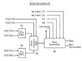
図1は、BCHコードを用いた2ビットエラー訂正3ビット以上エラー警告(2EC−EW)の動作モード(或いはシステム)を基本とし、これをパリティチェックコードを用いた1ビットエラー訂正2ビットエラー警告(1EC−2EW)の動作モード(或いはシステム)への切り換え可能としたメモリシステムの概要を示す。 FIG. 1 is based on the operation mode (or system) of 2
二つの動作モード(或いはシステム)は、回路要素の主要部を共用して、データ入力の切り換えやサブシステムのショートカットにより切り換えられる。以下の説明では、1EC−2EWの動作モード(或いはシステム)、2EC−EWの動作モード(或いはシステム)をそれぞれ単に、1ECシステム、2ECシステムという場合がある。 The two operation modes (or systems) can be switched by switching the data input or sub-system shortcut, sharing the main part of the circuit elements. In the following description, the operation mode (or system) of 1EC-2EW and the operation mode (or system) of 2EC-EW may be simply referred to as 1EC system and 2EC system, respectively.
メモリコア10aは、1EC−2EWシステム適用領域であり、メモリコア10bは、2EC−EWシステム適用領域である。即ちここでは、メモリコア10a,10bが一つのチップ内に別々に用意されて、これが用途に応じて使い分けられる場合を想定している。但しこれに限定されるわけではなく、メモリコア10a,10bが一体の領域であって、この一体のメモリ領域に対して1EC−2EWシステムと2EC−EWシステムとが選択的に適用されるものとしてもよい。 The
エンコード部11では、記憶すべきデータとの関係で、そのデータのエラーを検出するに必要な検査ビット(チェックビット)を生成する。2ECシステムの場合、データ多項式f(x)x16をコード生成多項式g(x)で割って、その剰余多項式r(x)の係数として16ビットのチェックビットを求める。1ECシステムの場合は、データ多項式f(x)x16をコード生成多項式h(x)で割って、その剰余多項式t(x)の係数として9ビットのチェックビットを求める。The
求められたチェックビットが情報ビットと共にメモリコア10a,10bのセルアレイに選択的に書き込まれる。 The obtained check bits are selectively written into the cell arrays of the
多項式ν(x)(2ECシステムの場合)或いはξ(x)(1ECシステムの場合)で表されるメモリコア回路10a,10bからの読み出しデータは、デコード部即ちシンドローム演算部12でエラーの有無を判定するためのシンドローム計算が行われる。2ECシステムの場合、二つの8次の原始多項式m1(x),m3(x)での剰余計算によるシンドロームが求められる。Read data from the
1ECシステムの場合は、ここでは、m3(x)での剰余を求める計算に代わって、m0(x)での剰余を求める計算、即ちメモリから読み出した128+9ビットのパリティを求める計算となるように、入力と出力の切り換えが行われる。In the case of the 1EC system, instead of the calculation for obtaining the remainder at m3 (x), the calculation for obtaining the remainder at m0 (x), that is, the calculation for obtaining 128 + 9-bit parity read from the memory. Thus, switching between input and output is performed.
得られたシンドロームに基づきエラー位置検索を行うエラー位置検索部13は、2段階のインデックス演算部13a,13bと、エラー訂正部14のサブシステムに分けられている。2ECシステムの場合に、本来の多項式の変数xに対してx=ασ1yなる変換変数yを導入して、エラー位置対応のインデックスynを求めるのが、最初の演算部13aであり、以下これを“ynロケータ(locator)”という。その演算結果に基づいて実際のエラービット位置iを求めるのが、次の演算部13bであり、以下これを“iロケータ”という。The error
これらサブシステムとしてのロケータは、計算規模を小さくするために、255を法とする加算を、17を法とする加算と15を法とする加算の並列処理として実現する。エラー訂正部14ではエラー位置のビットデータが反転される。 These locators as subsystems realize addition modulo 255 as parallel processing of
1ECシステムの場合、ynロケータ13aは、不要になる。そこでこの部分を非活性化してショートカットするため、この部分の駆動信号CLKをVssに固定すると同時に、次段への出力をインデックス“0”固定として、次段が誤った計算をしないようにする。iロケータ13bの部分は、入力の一方が“0”固定されて加算器から実質的にはデコーダになること以外、回路的な変更はない。For 1EC system,y n
2ECシステム及び1ECシステムの詳細を説明する前に、この実施の形態が適用されるメモリコアの具体構成を説明する。 Before describing the details of the 2EC system and the 1EC system, a specific configuration of a memory core to which this embodiment is applied will be described.
図2は、通常のNANDフラッシュメモリで用いられているのと同じメモリコアの構成を示している。このメモリコア回路は、セルアレイ1、センスアンプ回路2及びロウデコーダ3を有する。セルアレイ1は、直列接続されたメモリセルM0−M31を有するNANDセルユニット(NANDストリング)を配列して構成されている。NANDセルユニットNUの一端は選択ゲートトランジスタS1を介してビット線BLe(BLo)に、他端は選択ゲートトランジスタS2を介して共通ソース線CELSRCに接続されている。 FIG. 2 shows the same memory core configuration as that used in a normal NAND flash memory. The memory core circuit includes a
メモリセルの制御ゲートは、ワード線WL0−WL31に接続され、選択ゲートトランジスタS1,S2のゲートは選択ゲート線SGD,SGSに接続されている。ワード線WL0−WL31と選択ゲート線SGD,SGSを選択駆動するのがロウデコーダ3である。 The control gates of the memory cells are connected to the word lines WL0 to WL31, and the gates of the selection gate transistors S1 and S2 are connected to the selection gate lines SGD and SGS. The
センスアンプ回路2は、同時書き込み及び読み出しを行う1ページ分のセンスユニットSAを有する。各センスユニットSAには、ビット線選択回路4により、隣接するビット線BLe,BLoのいずれかが選択されて接続される。これにより、一つのワード線WLiと複数の偶数番ビット線BLe(或いは複数の奇数番ビット線BLo)により同時に選択されるメモリセルの集合が、同時に書き込み/読み出しが行われる1ページ(1セクタ)となる。非選択側のビット線は所定電位を与えたシールド線として利用することにより、選択ビット線間の干渉を防止することができる。 The
ワード線WL0−WL31を共有するNANDセルユニットの集合は、データ消去の単位とするブロックを構成し、図のようにビット線の方向に複数のブロックBLK0−BLKnが配置される。 A set of NAND cell units sharing the word lines WL0 to WL31 constitutes a block as a unit of data erasure, and a plurality of blocks BLK0 to BLKn are arranged in the bit line direction as shown in the figure.
図3は、この発明が適用される、別の動作原理によるNAND型フラッシュメモリのメモリコアを示している。メモリセルアレイ1は、センスアンプ2を挟んで配置されたセルアレイ1a,1bに分けられている。センスアンプ回路2には、電流検出型の差動センスアンプが用いられ、セルアレイ1a,1bの一方から選択された“情報セル”と他方から選択された“参照セル”との間でセル電流差を検出してデータセンスする方式としている。 FIG. 3 shows a memory core of a NAND flash memory according to another operation principle to which the present invention is applied. The
セルアレイ1aには、一つのビット線BLに、複数の情報セルNANDストリング,T−NANDと、少なくとも一つの参照セルNANDストリングR−NANDとが接続されている。セルアレイ1bには、セルアレイ1a側のビット線BLと対をなすビット線BBLに、複数の情報セルNANDストリング,C−NANDと、少なくとも一つの参照セルNANDストリングR−NANDとが接続されている。 In the cell array 1a, a plurality of information cell NAND strings T-NAND and at least one reference cell NAND string R-NAND are connected to one bit line BL. In the cell array 1b, a plurality of information cell NAND strings C-NAND and at least one reference cell NAND string R-NAND are connected to a bit line BBL paired with the bit line BL on the cell array 1a side.
情報セルT−cell,C−cellと参照セルR−cellとは同じメモリセル構造を有する。そして、セルアレイ1a,1bの一方から情報セルT−cell(またはC−cell)が選択されたときに、他方からは参照セルR−cellが選択される。 The information cells T-cell and C-cell and the reference cell R-cell have the same memory cell structure. When the information cell T-cell (or C-cell) is selected from one of the cell arrays 1a and 1b, the reference cell R-cell is selected from the other.
情報セルNANDストリングT−NAND,C−NAND及び参照セルNANDストリングR−NANDは、ビット線と直交する方向に複数個配列されて、セルブロックを構成する。セルブロックには共通に、ワード線TWL,CWL,RWLが配設される。 A plurality of information cell NAND strings T-NAND and C-NAND and reference cell NAND strings R-NAND are arranged in a direction orthogonal to the bit lines to constitute a cell block. The word lines TWL, CWL, and RWL are commonly provided in the cell blocks.
図4は、センスアンプSAUに接続される情報セルNANDストリングT−NAND(またはC−NAND)と参照セルNANDストリングR−NANDの具体構成を示している。それぞれ、複数個の直列接続された、電気的書き換え可能な不揮発性メモリセルM0−M31と、選択ゲートトランジスタSG1,SG2とを有する。同じ不揮発性メモリセルM0−M31を用いているが、情報セルNANDストリングT−NAND(またはC−NAND)ではこれらが情報セルT−cell(またはC−cell)として、また参照セルNANDストリングR−NANDでは参照セルR−cellとして用いられる。 FIG. 4 shows a specific configuration of the information cell NAND string T-NAND (or C-NAND) and the reference cell NAND string R-NAND connected to the sense amplifier SAU. Each has a plurality of non-volatile memory cells M0 to M31 connected in series and electrically rewritable, and select gate transistors SG1 and SG2. Although the same nonvolatile memory cells M0 to M31 are used, in the information cell NAND string T-NAND (or C-NAND), these are used as the information cell T-cell (or C-cell) and the reference cell NAND string R- In NAND, it is used as a reference cell R-cell.
図5は、4値記憶を行う場合のメモリセルのデータレベル(しきい値レベル)分布を示している。情報セルT−cell,C−cellには、4つのデータレベルL0,L1,L2,L3のいずれか一つが書かれる。参照セルR−cellには、例えばデータレベルL0とL1の間に設定された参照レベルLrが書かれる。 FIG. 5 shows the data level (threshold level) distribution of the memory cells when performing quaternary storage. Any one of four data levels L0, L1, L2, and L3 is written in the information cells T-cell and C-cell. In the reference cell R-cell, for example, a reference level Lr set between the data levels L0 and L1 is written.
4つのデータレベルL0−L3のビット割付は、情報セルT−cellとC−cellの間で異なる。例えば、4値データを上位ビットHBと下位ビットLBで(HB,LB)で表すものとして、セルアレイ1a側の情報セルT−cellでは、L0=(1,0),L1=(1,1),L2=(0,1),L3=(0,0)とされ、セルアレイ1b側の情報セルC−cellでは、L0=(0,0),L1=(0,1),L2=(1,1),L3=(1,0)とされる。 The bit allocation of the four data levels L0 to L3 is different between the information cells T-cell and C-cell. For example, assuming that the quaternary data is represented by (HB, LB) with the upper bit HB and the lower bit LB, in the information cell T-cell on the cell array 1a side, L0 = (1, 0), L1 = (1, 1) , L2 = (0, 1), L3 = (0, 0), and in the information cell C-cell on the cell array 1b side, L0 = (0, 0), L1 = (0, 1), L2 = (1 , 1), L3 = (1, 0).
図5には、読み出し時、情報セルT−cell,C−cellに読み出すべきデータに応じて与えられる読み出し電圧R1,R2,R3及び参照セルR−cellに与えられる読み出し電圧Rrを示している。また、書き込み時、情報セルT−cell,C−cellに書き込むべきデータに応じて与えられる書き込みベリファイ電圧P1,P2,P3及び参照セルR−cellに与えられる書き込みベリファイ電圧Prを示している。 FIG. 5 shows the read voltages R1, R2, and R3 given according to the data to be read to the information cells T-cell and C-cell and the read voltage Rr given to the reference cell R-cell at the time of reading. In addition, write verify voltages P1, P2, and P3 given according to data to be written to the information cells T-cell and C-cell at the time of writing and a write verify voltage Pr given to the reference cell R-cell are shown.
この様な4値データ記憶方式は、例えば画像データ等、大きなデータ保存量(大きなデータ領域)が要求される場合に好ましい。従ってこの方式では、チェックビット領域が小さい1ECシステムとする。これに対して、データの高い信頼性が要求される場合には、2値データ記憶方式とすることが好ましく、またチェックビット領域が大きい2ECシステムを適用する。 Such a four-value data storage method is preferable when a large data storage amount (large data area) is required, such as image data. Therefore, in this method, a 1EC system having a small check bit area is assumed. On the other hand, when high data reliability is required, a binary data storage method is preferable, and a 2EC system having a large check bit area is applied.
次に、2EC−EWシステムと1EC−2EWシステムの詳細を説明する。この実施の形態では、2EC−BCHシステムを1ECにも対応できるようするので、まず基本となる2EC−BCHシステムを説明する。 Next, details of the 2EC-EW system and the 1EC-2EW system will be described. In this embodiment, since the 2EC-BCH system can be adapted to 1EC, the basic 2EC-BCH system will be described first.
(2ECシステムのデータエンコーディング)
128ビットの情報データの2ビットエラーを検出訂正するに必要な2EC−BCHコードは、ガロア体GF(28)であり、使用するビット長は、28−1=255であり、チェックビットとしては16ビットが必要となる。(Data encoding of 2EC system)
The 2EC-BCH code necessary for detecting and correcting the 2-bit error in the 128-bit information data is Galois field GF (28 ), and the bit length to be used is 28 −1 = 255. Requires 16 bits.
ガロア体GF(28)の原始根をαとすると、これを根とする対応するGF(2)上の8次の原始多項式はm1(x)は、数1のように表される。即ち、αのべき乗とm1(x)によるxのべき乗の既約多項式がお互いに対応するGF(256)の要素となる。また、αの3乗を根とする8次の既約多項式としてm1(x)と互いに素な数1に示す多項式m3(x)を用いる。When the primitive root of the Galois field GF (28) and alpha, which 8-order primitive polynomial over GF (2) corresponding to the root m1 (x) is expressed as

これらの二つの原始多項式をもとに、2ビットエラー訂正可能なECCが構成される。書き込むべきデータに基づいてチェックビットを生成するには、コード生成多項式として、数2のようなm1(x)とm3(x)の積多項式g(x)を作る。Based on these two primitive polynomials, an ECC capable of 2-bit error correction is constructed. In order to generate check bits based on data to be written, a product polynomial g (x) of m1 (x) and m3 (x) as shown in
データとして利用できるビット数は、239ビットであり、これらをa16からa254としたとき、数3のような238次の情報多項式f(x)を作る。The number of bits that can be used as data is 239 bits, when they were froma 16 anda 254, making the
実際にはデータとして用いるのは、239ビット中例えば128ビットであり、このとき111ビットの係数は“0” に固定して対応する次数の項がない情報多項式となる。239の項数の情報多項式f(x)のうち、その係数を“0”に固定する111項として、どの次数を選ぶかによって、後述するデコード時のシンドローム計算の計算量が異なるのでこの選択のしかたが重要となる。 Actually, for example, 128 bits out of 239 bits are used as data. At this time, the coefficient of 111 bits is fixed to “0” and becomes an information polynomial having no corresponding degree term. Of the 239 term information polynomials f (x), the calculation amount of syndrome calculation at the time of decoding differs depending on which order is selected as the 111 term for which the coefficient is fixed to “0”. How is it important.
情報多項式f(x)からチェックビットを作るには、f(x)x16なる多項式をコード生成多項式g(x)で割った、数4に示すような15次の剰余多項式r(x)を求める。To make the check bits from an information polynomial f (x), divided by f(x) encodingx 16 becomes polynomial generator polynomial g (x), the
この剰余多項式r(x)の係数b15〜b0をチェックビットとして用いる。即ち、239から選ばれた128の係数ai(143)〜ai(16)を“情報ビット”とし、b15〜b0の16ビットを“チェックビット”として、下記数5に示す計144ビットがメモリに記憶させる“データビット”となる。The coefficients b15 to b0 of the remainder polynomial r (x) are used as check bits. That is, 128 coefficients ai (143) to ai (16) selected from 239 are set as “information bits”, and 16 bits b15 to b0 are set as “check bits”. The bit is a “data bit” to be stored in the memory.
ai(k)はメモリに外部から書き込むデータであり、このデータをもとに内部でチェックビットbjが作られ同時に書き込まれる。ai (k) is data to be written to the memory from the outside. Based on this data, check bits bj are internally created and written simultaneously.
(2ECシステムのデータデコーディング)
次に、メモリに記憶させた144ビットのデータからエラーを検出し2ビットのエラーまでを修正する方法について説明する。(Data decoding of 2EC system)
Next, a method of detecting an error from 144-bit data stored in the memory and correcting up to a 2-bit error will be described.
f(x)x16なる254次のデータ多項式の係数をメモリに記憶させてエラーが生じたとすれば、そのエラーも254次多項式で表される。このエラー多項式をe(x)とすれば、メモリから読み出したデータは、数6のような構造の多項式ν(x)になる。If the coefficients of f (x) x16 becomes 254 order data polynomial by storing in memory that an error occurs, the error is also expressed in 254-degree polynomial. Assuming that this error polynomial is e (x), the data read from the memory becomes a polynomial ν (x) having a structure as shown in
この数6のエラー多項式e(x)の係数が“1”の項がエラーとなる。即ち、e(x)を検出することがエラー検出と訂正を行なうことに相当する。 The term in which the coefficient of the error polynomial e (x) in
第一段階として、読み出しデータ多項式ν(x)を原始多項式m1(x),m3(x)で割って各々の剰余をS1(x),S3(x)とする。数7に示すように、これは、e(x)をm1(x),m3(x)で割った剰余に等しいことは、ν(x)の構造から明らかである。As a first step, the read data polynomial ν (x) is divided by the primitive polynomials m1 (x) and m3 (x), and the remainders are defined as S1 (x) and S3 (x). As shown in
この剰余S1(x)とS3(x)をシンドローム(syndrome)多項式という。The remainders S1 (x) and S3 (x) are referred to as syndrome polynomials.
2ビットのエラーがiとjビットにあるとすれば、エラー多項式は、e(x)=xi+xjである。この実施の形態においては、GF(256)の要素であるm1(x)=0の根αの指数(インデックス)に関するGF(256)内の計算でiとjを求める。If there are 2-bit errors in i and j bits, the error polynomial is e (x) = xi + xj . In this embodiment, i and j are obtained by calculation in GF (256) regarding the index (index) of the root α of m1 (x) = 0, which is an element of GF (256).
xnのm1(x)での剰余をpn(x)としたとき、αn=pn(α)である。下記数8に示すように、エラーの次数の対応するαi,αjのそれぞれをX1,X2とし、シンドロームS1(x),S3(x)に対してS1(α)とS3(α3)に対応する指数をσ1,σ3として、S1(α)とS3(α3)をそれぞれS1とS3とする。When the remainder of xn at m1 (x) ispn (x), αn = pn (α). As shown in the following
m3(α3)=0であることから、次の数9の関係式が得られる。Since m3 (α3 ) = 0, the following
第二段階として未知数X1とX2を根とする多項式ΛR(x)を考えると、数10のように、積X1X2がS1とS3で表現できるので、係数がsyndrome多項式から計算できる。Considering a polynomial ΛR (x) whose roots are unknowns X1 and X2 as the second stage, since the product X1 X2 can be expressed by S1 and S3 as shown in
第三段階としてΛR(x)のGF(256)での根となるαnを見つければ、X1,X2=αnからエラービット位置iやjがαnのnとして求められる。即ち、ΛR(αn)=0を、n=0〜254で探索してヒットした指数nがエラービットとなる。If αn that is the root of ΛR (x) at GF (256) is found as a third step, error bit positions i and j are obtained asn of αn from X1 , X2 = αn . In other words, the index n hit by searching for ΛR (αn ) = 0 withn = 0 to 254 becomes an error bit.
下記数11に示すように、1ビットエラーの時は、X1=S1,X13=S3=S13となり、エラー位置がS1からわかる。エラーがないときにはS1=S3=0となる。3ビット以上のエラーでその位置が計算出来ないときにはS1,S3の一方のみが0となるか、解となるnが存在しない。As shown in the following
(エラー位置検索)
エラー位置の検索は、ΛR(x)=0 となる根x=αnのインデックスnを求めることである。そのために、数10に示すΛR(x)を変形してインデックス関係だけでnを求めることが出来るようにする。具体的に、ΛR(x)=0を解くことは、これにx=ασ1yなる変数変換を施すことにより、下記数12の変数yを求めることと等価になる。(Error location search)
The search for the error position is to obtain the index n of the root x = αn such that ΛR (x) = 0. For this purpose, ΛR (x) shown in
この式を用いることより、変数計算から決まる指数とシンドローム計算から決まる指数とを直接比較して、一致する変数を見つけることができる。具体的には、数12を解くために、yにαnを代入して、下記数13のインデックスynを求める。By using this equation, it is possible to directly compare the index determined from the variable calculation and the index determined from the syndrome calculation to find a matching variable. More specifically, to solve the
そして、下記数14のように、シンドローム計算で求まるインデックスσ3−3σ1と変数計算から決まるインデックスynとを比較して、一致したnがエラー位置対応のyのインデックスということになる。Then, as in the following
この変数yのインデックスを本来の変数xのインデックスに戻すためには、下記数15のように、ασ1をyに掛ければよい。In order to return the index of the variable y to the original index of the variable x, ασ1 may be multiplied by y as shown in the following
数15のαのインデックスσ1+nが、エラー位置に対応するxのインデックスであり、このxに対して、ΛR(x)=0となる。The index σ1 + n of α in
図19は、インデックスnとynの対応関係をまとめたものである。nの順にynを並べたものと、ynの順にnを並べたものを合わせて示したが、後者はyn=0の場合を除いて同一のynに二つのnが対応することを示している。なお、nが85と170では対応するynはない(即ちガロア体の要素0に対応する)。またynの値が全ての255の剰余にわたっていないことが分かる。対応するynがない場合にはΛR(x)に解が存在しない。Figure 19 summarizes the correspondence between index n and yn. n and that arranged yn in the order of, showed together that arranged n the order of yn, that the two n corresponding to the
エラー位置検索で必要な計算はインデックスの合同式を解くことであり、二つの合同式を解く必要がある。はじめにシンドロームのインデックスからy2+y+1=αynのynを求める。次にこのynに対応するy=αnのインデックスnを対応関係で見つけたあと、x=ασ1yによってxのインデックスiを合同式を解いて求める。The calculation required for the error position search is to solve a congruence formula of indexes, and it is necessary to solve two congruence formulas. First determine they n ofy 2 + y + 1 = α yn from the index of the syndrome. Then after finding the index n of y = alphan corresponding to the yn in correspondence to the index i of x by x = alpha.sigma.1 y determined by solving the congruence.
合同式はいずれもGF(256)であるので255を法としたものである。この計算はまともに行なうと、255×255の規模の比較を行うことに相当し回路規模が大きくなる。そこで次のように計算を並列化する。 Since the congruence formulas are all GF (256), 255 is modulo. If this calculation is performed properly, it corresponds to the comparison of the scale of 255 × 255, and the circuit scale becomes large. Therefore, the calculation is parallelized as follows.
255を互いに素である二つの因子(整数)に分けて、これらを法とする二つの合同式に分離して、これらの合同式を同時に満たす数はもともとの合同式も満たすことを利用する。具体的に、255の二つの因子はできる限り差が小さいものとすることが好ましく、255=17×15によって、17と15をそれぞれ法とする合同式を同時に解く。 255 is divided into two factors (integers) that are relatively prime and separated into two congruence equations modulo these, and the fact that the number satisfying these congruence equations simultaneously satisfies the original congruence equation is also used. Specifically, it is preferable that the difference between the two factors of 255 is as small as possible, and a congruence equation modulo 17 and 15 is solved simultaneously by 255 = 17 × 15.
まず、ynを求めるには、数16の合同式を用いる。即ち、15倍したインデックス間の17を法とした加減算と、17倍したインデックス間の15を法とした加減算とを同時並行させる。First, inorder to obtain yn, the congruence formula of
次に、インデックスiを求めるには、数17の合同式を用いる。ここでも、15倍したインデックス間の17を法とした加減算と、17倍したインデックス間の15を法とした加減算とを同時並行させる。 Next, in order to obtain the index i, the congruence formula of
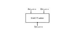
図1では、数16の加減算を並列的に行うのが、エラー位置検索部13内のynロケータ13aであり、数17の加減算を並列的に行うのが、iロケータ13bである。In Figure 1, the
次に、以上の2EC−BCHシステムに併用される1ビットエラー訂正2ビットエラー警告(1EC−2EW)システムを説明する。 Next, a 1-bit error correction 2-bit error warning (1EC-2EW) system used in combination with the above 2EC-BCH system will be described.
(1ECシステムのデータエンコーディング)
1ECシステムでは、2ECシステムの場合と同じ8次の原始多項式m1(x)と、αの0乗すなわち1を根とする1次の既約多項式としてm1(x)と互いに素な多項式m0(x)=x+1を用いる。(Data encoding of 1EC system)
In 1EC systems, a primitive polynomialm 1 (x) the same 8-order as in 2EC systems, polynomial disjoint andm 1 0 power i.e. 1 α as first-order irreducible polynomial rooted (x) mUse 0 (x) = x + 1.
これらの多項式を用いて、データにチェックビットを付加してエンコードする方法は、まず数18に示す、m1(x)とm0(x)の積多項式h(x)を作る。The encoding method using these polynomials with check bits added to the data first creates a product polynomial h (x) of m1 (x) and m0 (x) as shown in
データとして利用できるビット数は239ビットであり、これらをa16からa254として、数19に示す情報多項式f(x)を作る。The number of bits that can be utilized as data is 239 bits, these asa 254 froma 16, making shown in
2ECシステムの場合と同様、実際にデータとして使うビットは、128とし、111ビットの係数は0固定する。情報データ多項式からチェックビットを作るには、数20に示すように、f(x)x16なる多項式をh(x)で割った8次の剰余多項式t(x)の係数をc8〜c0として、これらの係数をチェックビットとして用いる。As in the case of the 2EC system, the number of bits actually used as data is 128, and the coefficient of 111 bits is fixed to zero. To make the check bits from the information data polynomial, as shown in several 20,
すなわち、下記数21に示すように、239から選ばれた128の係数ai(143)〜ai(16)と、c8〜c0の9ビットの計137ビットがメモリに記憶させるデータとなる。ai(k)がメモリに外部から書き込むデータでありこのデータをもとに内部でチェックビットcjが作られ同時に書き込まれる。That is, as shown in the following
数21に示すように、1ECシステムでは、2ECシステムで用いられるチェックビットのうち、b15〜b9は固定ビット“0”として、計128+9ビットがメモリに記憶される。即ち、b15〜b9の固定ビットはメモリには記憶させないので、2ECシステムに比べて、チェックビット領域は半分近く減少する。As shown in
(1ECシステムのデータデコーディング)
254次多項式の係数をメモリに記憶させてエラーが生じたとすれば、このエラーも254次多項式で表される。これをe(x)とすれば、メモリから読み出したデータは、数22のような多項式ξ(x)になる。(1EC system data decoding)
If an error occurs when the coefficient of the 254th order polynomial is stored in the memory, this error is also expressed by the 254th order polynomial. If this is assumed to be e (x), the data read from the memory becomes a polynomial ξ (x) as shown in
エラー多項式e(x)に含まれる多項式の次数を検出することがエラー検出と訂正を行なうことに相当する。第一段階として、数23に示すように、ξ(x)をm1(x),m0(x)で割って各々の剰余をS1(x),parityとする。Detecting the degree of the polynomial included in the error polynomial e (x) corresponds to performing error detection and correction. As a first step, as shown in
1ビットエラーの多項式をe(x)=xiとして、GF(256)の要素であるm1(x)の根αの指数(インデックス)計算でiを求めると、これがエラー位置になる。xnのm1(x)での剰余をpn(x)とするとき、αn=pn(α)であり、数24に示すように、エラーの次数の対応するαi をX1とし、シンドロームS1(x)に対してS1(α)に対応するインデックスをσ1として、S1(α)をS1とすると、S1=X1,parity=e(1)=1という関係が得られる。Assuming that a 1-bit error polynomial is e (x) = xi,i is obtained as an error position by calculating the index (index) of the root α of m1 (x) which is an element of GF (256). When the remainder of xn at m1 (x) is pn (x), αn = pn (α), and as shown in
parityはe(x)がゼロも含めて偶数個の項を含むときは0となり、特に2ビットエラーでは、parity=1+1=0となる。 The parity is 0 when e (x) includes an even number of terms including zero, and particularly for a 2-bit error, parity = 1 + 1 = 0.
第二段階として、X1=S1をインデックスについて解く。これは255を法とする合同式n≡σ1を満たすnを見つけることであり、これを満たすn=iがエラービットとなる。As a second step, X1 = S1 is solved for the index. This is to find n that satisfies the congruence formula n≡σ1 modulo 255, and n = i that satisfies this becomes an error bit.
このエラー検索に2ECのシステムをそのまま利用するので、255を互いに素である因数17と15に分けて、次の数25の合同式を満たすインデックスを求める。 Since the 2EC system is used as it is for this error search, 255 is divided into
この方法は、2ECシステムの場合と同じであり、図1ではエラー位置検索回路13のiロケータ13bの部分がその計算を行う。インデックスの和を計算する必要はないが、ゼロとの和を取る計算として実行できる。 This method is the same as in the case of the 2EC system. In FIG. 1, the
解の結果の判断は、数26のようになる。 The determination of the result of the solution is as shown in
ここまで、2ECシステムと、これと併用される1ECシステムの概要を説明したが、以下にはそれぞれのシステムの詳細な計算手法及び、2ECシステムと1ECシステムの切り換え手法の詳細を説明する。 Up to this point, the outline of the 2EC system and the 1EC system used in combination with the 2EC system has been described. In the following, detailed calculation methods of each system and details of the switching method between the 2EC system and the 1EC system will be described.
239の情報ビット全てを使用しないこの実施の形態のシステムでは、使用しないビットの選択がシンドローム計算等の計算量を決めることになる。デコードではシンドローム多項式の計算の後エラー位置を検索する演算などを行なうので、計算時間を短くするためにも計算量を出来るだけ少なくしたい。これは、情報多項式f(x)の中から、例えば最適な128個の項(次数)の選択を行なうことにより可能となる。 In the system of this embodiment that does not use all 239 information bits, selection of unused bits determines the amount of calculation such as syndrome calculation. In decoding, calculation of the syndrome polynomial is performed, and an operation for searching for an error position is performed. Therefore, in order to shorten the calculation time, it is desirable to reduce the calculation amount as much as possible. This is made possible by selecting, for example, the optimum 128 terms (orders) from the information polynomial f (x).
シンドローム多項式は同時に並列に計算を行なう。各多項式の各次数の係数の計算は“1”のパリティチェックであるので、どの次数の係数の計算もバラツキなくほぼ同じ時間で行なわれれば計算量は減る。 Syndrome polynomials are calculated in parallel at the same time. Since the calculation of the coefficient of each order of each polynomial is a parity check of “1”, the calculation amount is reduced if the calculation of the coefficient of any order is performed in substantially the same time without variation.
そのための選択の一つの方法は、シンドローム計算に用いられる7次の剰余多項式pn(x)とp3n(x)の係数が“1”の総和を、各nについて求め、総和の数の少ない方から必要なデータビット数だけのnを選択することである。2ECシステムであれば、最初の16個を検査ビットとしてx0〜x15の係数を使うので固定し、17個目以降の選択に係数の“1”の総和の昇順選択をする。One method of selection for this purpose is to obtain the sum of the coefficients of the seventh-order remainder polynomials pn (x) and p3n (x) “1” used for the syndrome calculation for each n, and the number of sums is small. Is to select n as many as the required number of data bits. If 2EC system, because it uses the coefficients of x0 ~x15 to secure the first 16 as check bits, the ascending selection of the sum of "1" of the coefficient selection of 17 onwards.
また、同じ総和の数のグループ内で選択が終了する際には、係数“1”がpn(x)とp3n(x)内で各次数の項の間に均等に分布するnを基準に同じ次数項での“1”の重なりが少ない順に選択する。すなわち基準となるnのpn(x),p3n(x)の係数“1”の次数での項の係数の総和が少ない順に選択する。Further, when selection is completed within the group of the same total number, the coefficient “1” is based on n that is evenly distributed between the terms of the respective orders in pn (x) and p3n (x). Are selected in ascending order of overlap of "1" in the same order term. That is, selection is made in the order of the sum of the coefficients of the terms in the order of the coefficient “1” of the reference n of pn (x) and p3n (x).
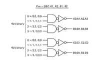
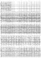
このような選択方法で選んだ254次のデータ多項式f(x)x16で144ビットデータを扱う場合に使用する、144個の次数nを、図6に示す。FIG. 6 shows 144 orders n used when 144-bit data is handled by the 254th order data polynomial f (x) ×16 selected by such a selection method.
この選択方法は必ずしもパリティチェックを行なう多項式の各次数の係数“1”の数の最大のものを最も少なくするとは限らないが、全ての組合せの中から計算ステップが最小となるものを探索する様な大規模な計算を必要としないでシンドローム計算回路規模を減らしかつ、シンドローム計算のステップ数を減らす簡便な方法ではある。 This selection method does not necessarily reduce the maximum number of coefficients “1” of each degree of the polynomial for which parity check is performed, but searches for a combination having the minimum calculation step from all combinations. This is a simple method for reducing the syndrome calculation circuit scale and reducing the number of steps of the syndrome calculation without requiring a large-scale calculation.
図7は、2ECシステムの場合のコード生成多項式g(x)の剰余rn(x)であって、選択されたxnの剰余rn(x)の各次数での係数が“1”であるnの表である。FIG. 7 shows the remainder rn (x) of the code generator polynomial g (x) in the case of the 2EC system, and the coefficient in each order of the remainder rn (x) of the selected xn is “1”. It is a table of some n.
例えば、x15の係数が“1”であるrn(x)の次数nは、図のm=15の列の係数“1”の数が1から62の欄に書かれている17,18,22,…,245,249,250である。チェックビットのx15の係数に相当するb15は情報データ多項式f(x)x16の中のこの選択されたn次の項の係数のパリティチェックの結果として得られる。For example, the order n of rn (x) in which the coefficient of x15 is “1” is the number of coefficients “1” in the column of m = 15 in the figure in the
図8は、1ECシステムの場合のコード生成多項式h(x)の剰余tn(x)であって、選択されたxnの剰余tn(x)の各次数での係数が“1”であるnの表である。例えばx8の係数が“1”であるtn(x)のnは表のm=8の列の係数1の数の欄の値が1から66に書かれている18,25,26,…,249,250,253のnである。FIG. 8 shows the remainder tn (x) of the code generation polynomial h (x) in the case of the 1EC system, and the coefficient in each order of the remainder tn (x) of the selected xn is “1”. It is a table of some n. For example n oft n (x) coefficientsx 8 is "1" is written from the value of the number of columns of rows of the
チェックビットのx9の係数に相当するc8は情報データの多項式f(x)x16の中のこの選択されたn次の項の係数のパリティチェックの結果として得られる。The c8 corresponding to the coefficient of check bit x9 is obtained as a result of the parity check of the coefficient of this selected n-th order term in the polynomial f (x) x16 of the information data.
この実施の形態では、エンコード部11において、図7に示したg(x)の剰余テーブルと図8のh(x)の剰余テーブルとで、チェックビットを生成するためのパリティチェック回路の入力部を切り換えることになる。 In this embodiment, in the
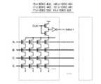
図9は、図1のエンコード部11における、情報データ多項式f(x)x16から、g(x)またはh(x)の剰余としてチェックビットを計算する際のパリティ・チェッカ・ラダー(parity checker ladder,以下PCLと略称する)21とその入力回路22である。FIG. 9 shows a parity checker ladder (parity checker) used when calculating a check bit as a remainder of g (x) or h (x) from the information data polynomial f (x) x16 in the
“1EC”は生成多項式h(x)を使用する1ECシステムの場合に“H”とするモード選択信号、“2EC”は生成多項式g(x)を使用する2ECシステムの場合に“H”とするモード選択信号である。 “1EC” is a mode selection signal that is “H” in the case of a 1EC system that uses the generator polynomial h (x), and “2EC” is “H” that is in the case of a 2EC system that uses the generator polynomial g (x). Mode selection signal.
16個の4ビットPCL21は、チェックビットを表す多項式の各次数の係数の値を計算するためのXOR回路の集合で、生成多項式によるxnの剰余のテーブルに従って各次数で入力を選択してそのパリティを計算する。The 16 4-
入力回路22は、クロックCLKでプリチャージされたノード20と、入力信号(記憶すべきデータ)である情報データ多項式の128個の係数信号ai(0)〜ai(127)をインバータで反転した信号をゲート入力としてノード20を放電するためのトランジスタMN1とを有する。どの係数を放電信号として選択するかは2ECシステムと1ECシステムの場合で異なるので、モード選択信号2ECと1ECで選択されるトランジスタMN3とMN2を、トランジスタMN1とノード20との間に介在させている。The
2ECシステムの場合は、チェックビット多項式は15次、1ECの場合は8次であるので、m=0〜8次までの4ビットPCL21は、1EC,2EC共用である。従ってこの範囲では、入力信号をモード選択信号1ECと2ECで切り換える。即ちこれらのパリティチェック回路群の入力回路22は、2ECと1ECとでその構成が変更される。 In the case of the 2EC system, the check bit polynomial is of the 15th order and in the case of 1EC is the 8th order, so the 4-
m=9〜15次は2ECシステムの場合のみ入力が有効で、1ECのときは入力固定状態即ち、プリチャージ状態から変化せずに働かないようにされる。 For m = 9 to 15th order, the input is effective only in the case of the 2EC system, and in the case of 1EC, the input is fixed, i.e., the precharge state is kept unchanged.
図10は、4ビットPCL21の一例を示す。2ECについての場合が主構成であり、これの初段入力が図9で説明した切り換え回路で1ECと2ECとで切り替わる。2ECの場合、図7に示すように、xmのm=11,5,2は、パリティチェックするビット数が最大の72個であるので、ここではこの場合を例として示す。各mについて、図7の表からnを選択し、係数anを用いてパリティチェックを行なう。FIG. 10 shows an example of the 4-
入力の数が4の剰余系のいずれに属するかによって用いるパリティ・チェッカ(PC)を組合せる。すなわち4で割り切れれば4ビットPCのみで、1が余れば2ビットPCの一方の入力端子をVdd にしたもの(すなわちインバータ)を加え、2が余れば2ビットPCを加え、3が余れば4ビットPCのひとつの入力端子をVdd にしたものを加える。 A parity checker (PC) to be used is combined depending on which of the 4 residue systems the number of inputs belongs to. That is, if it is divisible by 4, only 4-bit PC is added. If 1 is left, one input terminal of 2 bits PC is set to Vdd (ie, an inverter), and if 2 is left, 2-bit PC is added and 3 is If there is a remainder, a 4-bit PC having one input terminal set to Vdd is added.
m=11,5,2の例では、72入力であるので、初段は4ビットPCを18個、2段目は18入力となり4ビットPCを4個と2ビットPCを1個、3段目は5入力となるので4ビットPCを1個とインバータ、4段目は2入力なので2ビットPCで構成される。 In the example of m = 11, 5 and 2, since there are 72 inputs, the first stage has 18 4-bit PCs, the second stage has 18 inputs, 4 4-bit PCs and 1 2-bit PC, 3rd stage Since it has 5 inputs, it has one 4-bit PC and an inverter, and since the fourth stage has 2 inputs, it consists of 2-bit PC.
図11(a),(b)は、2ビットPCの回路構成とその回路記号である。これは、2ビットの信号a,bをXOR回路とXNOR回路でロジック演算して、“1”の数が偶数のときに出力ノードEPに“1”(even-parity)を出力する。 FIGS. 11A and 11B show the circuit configuration of a 2-bit PC and its circuit symbol. This is a logic operation of the 2-bit signals a and b by the XOR circuit and the XNOR circuit, and outputs “1” (even-parity) to the output node EP when the number of “1” is an even number.
図12(a),(b)は、4ビットPCの回路構成とその回路記号を示している。これは、4ビットの信号a,b,c,dを、二つずつのXOR回路とXNOR回路でロジック演算して、“1”の数が偶数であるときに、出力ノードEPに“1”を出力する。 FIGS. 12A and 12B show the circuit configuration of 4-bit PC and its circuit symbol. This is because four-bit signals a, b, c and d are logically operated by two XOR circuits and two XNOR circuits, and when the number of “1” is an even number, “1” is output to the output node EP. Is output.
次に、読み出しデータのエラー検出のためのデコード部、即ちシンドローム演算部12の詳細を説明する。 Next, details of the decoding unit for detecting errors in the read data, that is, the
図13はシンドローム多項式S1(x)の計算で使用する7次の剰余多項式pn(x)の選択されたnでの各次数の係数“1”のnの表である。例えばx7の係数が“1”であるpn(x)の次数nは、表のm=7の列の係数1の数の1から56の欄に書かれている7,11,12,…,237,242,245である。シンドローム多項式S1(x)のx7の係数はデータ多項式ν(x)の中のこの選択されたn次の項の係数のパリティチェックの結果として得られる。FIG. 13 is a table of n of coefficients “1” of the respective orders at selectedn of the seventh-order remainder polynomial pn (x) used in the calculation of the syndrome polynomial S1 (x). For example, the order n of pn (x) where the coefficient of x7 is “1” is 7, 11, 12, and the
図14は、シンドローム多項式S3(x)の計算で使用する、7次の剰余多項式p3n(x)の選択されたnにおける各次数の係数が“1”であるnの表である。例えば、x7の係数が“1”であるp3n(x)のnは表のm=7の列の係数1の数の欄の数が1から58の行に書かれている4,8,14,…,241,242,249である。S3(x)のx7の係数に相当する(s3)7は、データの多項式ν(x)の中のこの選択されたn次の項の係数のパリティチェックの結果として得られる。FIG. 14 is a table of n in which the coefficient of each degree in the selectedn of the seventh-order remainder polynomial p3n (x) used in the calculation of the syndrome polynomial S3 (x) is “1”. For example,n of p3n (x) where the coefficient of x7 is “1” is written in the rows of 1 to 58 in the column of the number of
1ECの場合は128+9ビットのデータのパリティチェックを行なうので、この数に等しい入力を持ったPCLが必要である。図14から分かるように、m=2とm=5の入力はそれぞれ64と73なので、和が137の所望値になる。そこで1ECの場合はこの次数の4ビットPCLを利用してデータビットのパリティチェックを行なう。 In the case of 1EC, since a parity check of 128 + 9-bit data is performed, a PCL having an input equal to this number is required. As can be seen from FIG. 14, since the inputs of m = 2 and m = 5 are 64 and 73, respectively, the sum becomes a desired value of 137. Therefore, in the case of 1EC, the parity check of the data bits is performed using this order of 4-bit PCL.
図15は、図1のシンドローム演算部12に用いられるパリティ・チェッカ・ラダー(PCL)31とその入力回路32の構成であり、上述のように1ECではm=2とm=5を利用してパリティチェックを行なう。即ち、m=2,5のPCL31は、1ECシステムと2ECシステムとで共用され、それ以外のPCLは2ECシステム専用となる。 FIG. 15 shows the configuration of the parity checker ladder (PCL) 31 and its
PCL31の入力回路32は、基本的に図9に示しチェックビット生成部と同じであり、クロックCLKでプリチャージされたノード30と、これに接続されて入力信号であるデータd0〜d15,di(0)〜di(127)をインバータで反転した信号をゲート入力とする、放電用トランジスタMN1とを有する。どの係数を放電信号として選択するかは2ECシステムと1ECシステムの場合で異なるので、モード選択信号2ECと1ECで選択されるトランジスタMN3とMN2を、トランジスタMN1とノード30との間に介在させている。The
モード選択信号1ECと2ECで入力回路構成を変更するのは、m=2,5のラダー入力部であり、1ECの場合その出力(s3)2,(s3)5は更に、2ビットPCに入力される。その出力は反転されているので、更にNANDゲートで1ECの場合のみ、pariry出力が得られるようになっている。2ECの場合は、NANDゲートにより、常にparity=“1”となる。The input circuit configuration is changed by the mode selection signals 1EC and 2EC in the ladder input section of m = 2, 5. In the case of 1EC, the outputs (s3)2 and (s3)5 are further input to the 2-bit PC. Is done. Since the output is inverted, a parity output can be obtained only when the NAND gate is 1EC. In the case of 2EC, the parity is always “1” due to the NAND gate.
1ECの場合、その他のPCLは入力が固定されて非活性とされる。またチェックビットは9ビットのみ用いられるので、入力データのうち、d9〜d15は、“0”として扱われる。In the case of 1EC, the input of other PCLs is fixed and deactivated. Since only 9 check bits are used, d9 to d15 of the input data are treated as “0”.
図15に示したシンドローム形成用のパリティ・チェッカ・ラダー(PCL)の具体的な例を2ECの場合について図16に示す。 FIG. 16 shows a specific example of the parity checker ladder (PCL) for syndrome formation shown in FIG. 15 in the case of 2EC.
図14から、xmのm=5は、パリティチェックするビット数が最大の73個であるのでこの場合を例として示す。x3nのm1(x)の剰余多項式p3n(x)のm次項の係数が“0”でないnは表にしてあるので、各mについて表からnを選択し、dnを用いてパリティチェックを行なう。From FIG. 14, m = 5 of xm, since the number of bits for parity checking is an 73 amino maximum shows this case as an example. Since n coefficients of m-order term of the remainder polynomialp 3n (x) is not "0" ofm 1 in x3n (x) is are tabulated, and select n from the table for each m, parity withd n Check.
m=5の例では73入力であるので、この場合も4段のパリティチェック回路で構成する。初段は、4ビットPCを18個とインバータとで構成する。2段目は19入力となるので、4ビットPCを4個と4ビットPCの一つの入力端をVddとしたものとで構成する。3段目は5入力となるので4ビットPCを1個とインバータで構成する。4段目は2入力となるので、2ビットPC一つで構成する。4段目出力が、シンドローム係数(s3)mとなる。In the example of m = 5, there are 73 inputs, and in this case also, a 4-stage parity check circuit is configured. The first stage consists of 18 4-bit PCs and inverters. Since the second stage has 19 inputs, it is composed of four 4-bit PCs and one 4-bit PC input terminal set to Vdd. Since the third stage has 5 inputs, one 4-bit PC is composed of an inverter. Since the fourth stage has two inputs, it is composed of one 2-bit PC. The fourth stage output is the syndrome coefficient (s3)m .
図17は、シンドローム多項式S1(x)の計算で使用する、xnのm1(x)での剰余pn(x)の選択されたnでの各次数における係数が“1”であるnの表であり、図13と同じものを示しているが、1ECの場合は、ν(x)の中のn=9から15は“0”固定として扱うので、破線で囲んだ部分は使われない。FIG. 17 shows that the coefficient in each order at the selectedn of the remainder pn (x) at m1 (x) of xn used in the calculation of the syndrome polynomial S1 (x) is “1”. 13 is the same table as FIG. 13, but in the case of 1EC, since n = 9 to 15 in ν (x) are treated as “0” fixed, the portion enclosed by the broken line is used. I will not.
図18は、シンドロームS1(x)の計算で用いられる4ビットPCLの構成例を示す。xmのm=6,2は図17からパリティチェックするビット数が最大の66個であるのでこの場合を例として示している。各mについて表からnを選択しdnを用いてパリティチェックを行なう。結果が係数(s1)mとなる。FIG. 18 shows a configuration example of the 4-bit PCL used in the calculation of the syndrome S1 (x). m = 6, 2 of xm is the number of bits to be parity checked from Figure 17 is shown as an example in this case since it is 66 up. Performing a parity check with dn to select the n from the table for each m. The result is the coefficient (s1)m .
入力の数が4の剰余系のいずれに属するかによって用いるパリティチェッカ(PC)を組合せる。すなわち4で割り切れれば4ビットPCのみで、1が余れば2ビットPCの一方の入力端子をVdd にしたものすなわち、インバータを加え、2が余れば2ビットPCを加え、3が余れば4ビットチPCのひとつの入力端子をVddにしたものを加える。 A parity checker (PC) to be used is combined depending on which of the 4 residue systems the number of inputs belongs to. In other words, if it is divisible by 4, only 4-bit PC is used. If 1 is left, one input terminal of 2-bit PC is set to Vdd. That is, an inverter is added, and if 2 is left, 2-bit PC is added and 3 is left. If this is the case, the input terminal of a 4-bit PC is set to Vdd.
m=6,2の例では66入力であるので、最初の段は4ビットPCを16個と2ビットPCを1個用いる。2段目は17入力となり、4ビットPCを4個とインバータを1個、3段目は5入力となるので4ビットPCを1個とインバータ、4段目は2入力となるので2ビットPCで構成される。 Since there are 66 inputs in the example of m = 6, 2, the first stage uses 16 4-bit PCs and 1 2-bit PC. The second stage has 17 inputs, 4 4-bit PCs and 1 inverter, and the third stage has 5 inputs, so one 4-bit PC and inverter, and the 4th stage has 2 inputs, so 2 bits PC Consists of.
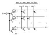
次に、シンドローム情報からエラー位置検索を行う図1のエラー位置検索部13及びエラー訂正部14の詳細を、図20〜図22を参照して説明する。 Next, details of the error
図20はynロケータ13a、図21はiロケータ13bを示し、図22はエラー訂正部14を示している。それぞれの回路入力部には、プリデコーダを配置して、各回路規模が小さくなるようにしている。Figure 20 isy n
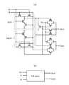
ynロケータ13aは、図20に示すように、シンドロームS1,S3をそれぞれデコードするプリデコーダ41,42と、そのデコード出力を並列演算する、17を法とするインデックス加算部43と15を法とするインデックス加算部44を有する。これらのインデックス加算部43,44は、数16の二つの合同式を同時に解く部分、即ち2ECのときの2つのエラーインデックスynを計算する部分である。yn locators 13a, as shown in FIG. 20, a
これらの加算部43,44は、NANDゲート45によって、モード選択信号2ECが“H”のときのみ活性になり、1ECの時にはECCクロックが供給されず不活性とされる。 These
一方のインデックス加算部43は、シンドロームのプリデコード結果をデコードして、インデックスに直す15σ3デコード部432と、−45σ1デコード部431と、これらに対応したインデックス−バイナリ変換部434,433と、得られたバイナリデータを17を法として加える5ビット(mod17)加算器435とを有する。One
もう一方のインデックス加算部44は、シンドロームのプリデコード結果をデコードして、インデックスに直す17σ3デコード部442と、−51σ1デコード部441と、これらに対応したインデックス−バイナリ変換部444,443と、得られたバイナリデータを15を法として加える4ビット(mod15)加算器445とを有する。The other
プリデコーダ兼スイッチ51は、5ビット加算器435の出力のうちの下位4ビット{15yn(17)}0−3と、4ビット加算器445の4ビット出力{17yn(15)}0−3のプリデコードを行う。ynロケータ13aが不活性の時は、プリデコーダ兼スイッチ51が、加算器435,445の出力を“0”に相当するように設定して、iロケータ13bに渡す働きをする。The predecoder /
図21に示すiロケータ13bは、エラー位置のインデックスiを計算する部分であり、前述のように2ECと1ECとで共通に用いられる。これは、数17の二つの合同式を並列演算で解く部分であり、17を法とするインデックス加算部52と、15を法とするインデックス加算部53とを有する。 The
インデックス加算部52は、プリデコーダ51の出力DEC2と、5ビット加算器435の最上位ビット{15yn(17)}4をデコードするyn(17)デコード部521と、シンドロームS1のデコード出力DEC1をデコードする15σ1デコード部522と、これらに対応したインデックス−バイナリ変換部523,524,525と、そのバイナリデータを17を法として加算する二つの5ビット(mod17)加算器526,528とを有する。更に、変換部523の出力には、計算不可能状態(No-Index17)を検出するための検出部527が接続されている。The
もう一つのインデックス加算部53は同様に、yn(15)デコード部531と、17σ1デコード部532と、これらに対応したインデックス−バイナリ変換部533,534,535と、そのバイナリデータを15を法として加算する二つの4ビット(mod15)加算器536,538と、変換部533の出力から、計算不可能状態(No-Index15)を検出する検出部537とを有する。Similarly, another
エラー訂正部14は、図22に示すように構成される。即ち、iロケータ13bの二つの5ビット加算器526,528の下位4ビット出力{15i(17)}0−3と、2つの4ビット加算器536,538の4ビット出力{17i(15)}0−3がプリデコーダ61,62でデコードされる。そのプリデコード出力と、二つの5ビット加算器526,528の最上位ビット出力{15i(17)}4とが、エラー位置デコード部63に入る。The
エラー位置デコード部63の出力がエラービット位置であり、データ訂正回路64においてメモリコアから読み出されたデータdkがその位置で訂正(反転)されて出力される。データ訂正回路64には、計算不可能状態信号Non-Index(17),(15)、シンドロームS1,S3、1ECparityも入り、訂正不可能(Non-correctable)信号を出力できるようになっている。 The output of the error
プリデコーダ41,42,61,62は、8ビットで表される256のバイナリ信号状態を、Ai,Bi,Ci,Di(i=0〜3)の組合せとして表す変換を行うものであり、図23に示すようにNAND回路で構成される。即ち8ビットのバイナリを2ビットずつ下位から区切り、4進数として表して、これらをAi,Bi,Ci,Diとしている。これらのプリデコーダを用いることにより、次のデコーダのトランジスタ数を8から4に半減させることができる。 The
15σ3 デコード部432,−45σ1デコード部431,17σ3 デコード部442,−51σ1 デコード部441,15σ1 デコード部522は、全て図24に示すように構成され、入力信号が異なるのみである。即ちプリデコード出力Ai−Diを選択的にゲート信号とするトランジスタを直列したNAND回路を各剰余類に属する既約多項式の数だけ並列接続して構成される。The 15σ3 decoding unit 432, −45σ1 decoding unit 431, 17σ3 decoding unit 442, −51σ1 decoding unit 441, 15σ1 decoding unit 522 are all configured as shown in FIG. 24, and only the input signals are different. . In other words, NAND circuits in which transistors having predecode outputs Ai-Di as selective gate signals in series are connected in parallel by the number of irreducible polynomials belonging to each remainder class.
クロックCLKにより制御されるプリチャージトランジスタにより共通ノードをプリチャージし、その放電の有無で剰余類のインデックス信号“index i”とする。信号配線Ai,Bi,Ci,Di(i=0〜3)が配設され、これがNAND回路を構成するトランジスタのゲートにデコードのコードに従って接続される。 The common node is precharged by a precharge transistor controlled by the clock CLK, and a remainder index signal “index i” is determined by the presence or absence of the discharge. Signal wirings Ai, Bi, Ci, Di (i = 0 to 3) are provided, and these are connected to the gates of the transistors constituting the NAND circuit according to the decoding code.
インデックス−バイナリ変換部433,434,443,444,523−525,533−535は、剰余類のインデックス信号“index i”を、2進数表示に変換するもので、図25のように構成される。変換されたバイナリ情報を保持するために、クロックCLKでリセットされるラッチ回路251が設けられている。インデックスが入力されない場合は5バイナリ回路なら2進数の31、4バイナリ回路なら、2進数の15である全ての信号が“H”状態を維持する。 The index-
図26は、17を法として、その剰余としての和を求める5ビット加算器(mod17)435,526,528の構成を示し、図27はその回路記号を示している。図示のように、この5ビット加算器は、5ビットの第1段加算回路71と、その和が17以上であることを検出して桁上げする桁上げ補正回路72と、この桁上げ補正回路72と共に、和が17以上の場合に32に対する17の補数15(=32−17)を加えるための第2段加算回路73とを有する。 FIG. 26 shows the configuration of 5-bit adders (mod 17) 435, 526, and 528 that calculate the sum as the remainder using 17 as a modulus, and FIG. 27 shows the circuit symbols. As shown in the figure, this 5-bit adder includes a 5-bit first
桁上げ補正回路72は、第1段加算回路71の出力状態に応じて、信号PF0を発生するものである。具体的にいえば、第1段加算回路71の最上位ビット出力S4’が“1”でありかつ、それ以外のビット出力S0,S1’〜S3’の少なくとも一つが“1”であること、即ち和が17以上であることを検出して、信号PF0(=“H”)を発生するように構成されている。 The
第2段加算回路73は、第1段加算回路71の出力が17以上の場合に、17の補数(01111)を加えるというロジックが組まれている。 The second
図28は、15を法として、その剰余としての和を求める4ビット加算器(mod15)445,536,538の構成を示し、図29はその回路記号を示している。この4ビット加算器は、4ビットの第1段加算回路81と、その和が15以上であることを検出して桁上げする桁上げ補正回路82と、この桁上げ補正回路82と共に、和が15以上の場合に16に対する15の補数1(=16−15)を加えるための第2段加算回路83とを有する。 FIG. 28 shows the configuration of 4-bit adders (mod 15) 445, 536, and 538 that calculate the sum as a remainder using 15 as a modulus, and FIG. 29 shows the circuit symbols. This 4-bit adder includes a 4-bit first
桁上げ補正回路82は、第1段加算回路81の出力状態に応じて、信号PF0を発生するものである。具体的にいえば、第1段加算回路82の出力S0’〜S4’が“1”であること、即ち和が15以上であることを検出して、信号PF0(=“H”)を発生する。 The
第2段加算回路83は、第1段加算回路81の出力が15以上の場合に、15の補数(0001)を加えるというロジックが組まれている。 The second
図26及び図28に示す加算器は、クロック同期が必要でなく、入力が確定すれば出力も確定するように構成されている。これにより、システムのタイミング制御の負担を減らすことができる。 The adders shown in FIGS. 26 and 28 are configured so that clock synchronization is not necessary and the output is determined when the input is determined. Thereby, the burden of timing control of the system can be reduced.
図26−29に示した加算器に用いられるフルアダー及びハーフアダーはそれぞれ、図30(a)(b)及び図31(a)(b)に示されている。フルアダーは、加えるビットAとBをXORとXNOR回路でロジック演算を行い、桁上げ信号Cinとのロジックを更に取って出力としてA,B,Cinの和Soutと桁上げ信号Coutを出力する。ハーフアダーは、一般的なロジックゲートで構成される。 The full adder and half adder used in the adder shown in FIGS. 26-29 are shown in FIGS. 30 (a) (b) and 31 (a) (b), respectively. The full adder performs logic operation on the bits A and B to be added by the XOR and XNOR circuits, further takes the logic of the carry signal Cin, and outputs the sum Sout of A, B and Cin and the carry signal Cout as outputs. The half adder is composed of a general logic gate.
図32は、ynロケータ13aの出力段のプリデコーダ兼スイッチ51の構成である。4ビット加算器(mod15)445の4ビット出力と、5ビット加算器(mod17)の下位4ビット出力とをデコーダするもので、その基本は図23のプリデコーダと同様である。Figure 32 is a configuration of the output stage of predecoder and switch 51 of they n
1ECの場合は、ynロケータ13aは不活性とされるので、インデックス−バイナリ変換部443,444の出力は15、インデックス−バイナリ変換部433,434の出力は31となる。このとき4ビット加算器445の出力は、15+15≡0(mod15)であり、5ビット加算器435の出力は、31+31≡11(mod17)となる。従って、次のiロケータ13bに“0”を渡すためには、モード選択信号2ECが入るNANDゲートG11,G12を用いて、1ECの場合には11のプリデコードに相当するC3とD2を強制的に“0”とする。For 1EC, sincey n
図33は、iロケータ13bのyn(17)デコード部521及びyn(15)デコード部531の構成を示している。これらは基本的に、ynロケータ13aの17σ3デコード部442と同じであるが、エラー数が二つの場合に相当して2つの剰余類インデックスが選択される。このため同時選択のインデックス信号がバスでぶつからないようにデコードする。即ち、同じ剰余類インデックス“index i”をindex i(bs1)とindex i(bs2)の二つに分ける。Figure 33 is,y n (17) of the
また剰余類の要素は15と17の剰余であるので、9ビットのバイナリで指定されるが、17の剰余の16のみで最上位ビットに相当する5ビット(17)加算器の出力{15yn(17)}4が“1”であることを利用して、剰余類の要素が16である場合には信号Ci,Diに代わって{15yn(17)}4を用いる。これにより、4段NANDでデコード部が構成される。Since the elements of the remainder class are the remainders of 15 and 17, they are specified by 9-bit binary, but only the
剰余類インデックスがないときはエラー位置探索が出来ない場合であり、これを識別するのがno-index検出部527,537である。これらは図34に示すように、インデックス−バイナリ変換出力の全ビットが“1”となることを検出するNAND回路で構成される。バスbs1,bs2には必ず同時に信号が発生するので一方、例えばバスbs1の状態のみをモニターしていれば十分である。 When there is no remainder class index, the error position search cannot be performed, and the no-
図35は、エラー訂正部14におけるエラー位置デコーダ63の構成を示している。ここでは、バスbs1,bs2にプリデコードされた4ビット(15)加算器536,538と、5ビット(17)加算器526,528からの信号Ai,BiとCi,Di,{15i(17)}4をデコードしてエラー位置信号αi(k)を発生する。FIG. 35 shows the configuration of the
プリデコードしない5ビット(17)加算器526,528の出力{15i(17)}4も使用するのは、yn(17)デコーダなどと同じ剰余類要素16のためである。Ai,Bi,Ci,Diの組合せはバスbs1とbs2によらないので、バス間のAi,BiとCi,DiのNANDノード間を接続してデコードしている。The reason why the output {15i (17)}4 of the 5-bit (17)
図36は、エラー訂正回路64の構成である。これは、1ECか2ECかによって動作が異なる。2ECの場合、シンドローム係数S1×S3が0でなければ1つ又は2つのエラーが発生しておりデータ訂正を行なう。S1×S3=0の場合は二つに別れる。S1=S3=0であればエラー無しでデータを修正する必要は無い。S1又はS3の一方のみが0であれば、3ビット以上のエラーが発生しており修正は不可能である。またエラー位置探索が不可能なno-index(17)又はno-index(15)が“1”のときも3ビット以上のエラーが発生しており修正は不可能である。 FIG. 36 shows the configuration of the
これらの場合の動作を判別するために、シンドローム多項式の係数(s1)mと(s3)mの係数がすべて“0”の場合を検出するNORゲートG1,G2が用いられている。3ビット以上のエラーがある場合は、ゲートG1,G2の一方の出力が“0”となる。これを受けて、NORゲートG6が訂正不能(non-correctable)を示す“1”を出力する。このとき、NORゲートG5の出力は“0”となり、エラー訂正を行うデコード用NANDゲートG7を非活性にする。In order to discriminate the operation in these cases, NOR gates G1 and G2 for detecting the case where the coefficients (s1)m and (s3)m of the syndrome polynomial are all “0” are used. When there is an error of 3 bits or more, one output of the gates G1 and G2 becomes “0”. In response to this, the NOR gate G6 outputs “1” indicating non-correctable. At this time, the output of the NOR gate G5 becomes “0”, and the decoding NAND gate G7 that performs error correction is deactivated.
エラーがない場合は、ゲートG1,G2の出力が共に“1”となり、NORゲートG4,G5ともに“0”を出力し、デコード用NANDゲートG7を非活性にする。 When there is no error, the outputs of the gates G1 and G2 are both "1", the NOR gates G4 and G5 are both output "0", and the decoding NAND gate G7 is deactivated.
1又は2ビットのエラーがある場合、ゲートG1,G2の出力は共に“0”となり、NORゲートG5の出力“1”がデコード用NANDゲートG7を活性にする。αi(k)で選択されたビット位置のデータdkを反転する反転回路として、2ビットパリティチェック回路361を用いて、エラーがない場合はdkをそのまま、エラー位置ではこれを反転して出力する。When there is an error of 1 or 2 bits, the outputs of the gates G1 and G2 are both “0”, and the output “1” of the NOR gate G5 activates the decoding NAND gate G7. A 2-bit
1ECの場合は、シンドローム計算回路の設定から、シンドローム係数s3がゼロになることはなく、信号No-Index (17), No-Index (15)が“0”に設定されるので、S1がゼロ以外の1ECparity信号が“1”(即ち1ECモード)のときに、ゲートG5の出力が“H”となりエラー訂正を行う。1ECparityが“0”のときは2ビットエラーであるので、訂正不能(non−correctable)信号を発生する。 In the case of 1EC, since the syndrome coefficient s3 is not zero and the signals No-Index (17) and No-Index (15) are set to “0” from the setting of the syndrome calculation circuit, S1 is zero. When the 1ECparity signal other than 1 is “1” (that is, 1EC mode), the output of the gate G5 becomes “H” and error correction is performed. When 1ECparity is “0”, it is a 2-bit error, and therefore a non-correctable signal is generated.
図37は、ynロケータ13a内の一方のインデックス加算部43の具体構成例を示している。17を法とするこのインデックス加算部43では、シンドロームのインデックスσ3とσ1から剰余類インデックス15σ3−45σ1(mod17)を求める。Figure 37 shows one specific example of the configuration of the
入力はインデックスσ3であり、シンドローム計算で得られた7次の多項式の係数(s3)m(m=0〜7)をデコード部432でデコードして、15σ3の17を法としての剰余類のインデックス位置の入力信号として選択する。そのインデックスをバイナリ変換部434で2進数に変換して、5ビットの数値をバス201に発生する。17の剰余類なので選択回路数は17個となる。The input is the index σ3 , and the coefficient (s3)m (m = 0 to 7) of the seventh-order polynomial obtained by the syndrome calculation is decoded by the
制御入力はインデックスσ1であり、シンドローム計算で得られた7次の多項式の係数(s1)m(m=0〜7)をデコード部431でデコードして、−45σ1の17を法としての剰余類のインデックス位置の制御信号として選択する。そのインデックスをバイナリ変換部433で2進数に変換して、5ビットの数値をバス202に発生する。17の剰余類なので選択回路数は17個となる。The control input is the index σ1 , and the coefficient (s1)m (m = 0 to 7) of the seventh-order polynomial obtained by the syndrome calculation is decoded by the
バス201,202に得られた2進数データは、5ビット(17)加算器435に入り、和が求められて、17を法とした数値がバス203に出力される。即ち出力は、15ynの17を法としての類を示すインデックスの2進数表示である。The binary data obtained on the
図38は、既約剰余pn(x)のインデックスnを15倍して法17の剰余類15n(17)として分類したものである。0から16のインデックスで分類され、各々の類には15個のnが含まれこれらに対応するpn(x)の各次数の係数に従ってプリデコーダされた信号Ai,Bi,Ci,Diの各i(=0〜3)を示した。In FIG. 38, the index n of the irreducible residue pn (x) is multiplied by 15 to classify it as the
これらの信号Ai,Bi,Ci,Diでインデックス加算部43のデコードトランジスタのゲートへの信号接続が決まる。例えばインデックス1においては並列にNOR接続されるNANDのノードは、nが161,59,246,127,42,93,178,144,212,229,110,195,8,76,25に相当し、NANDのトランジスタゲートへは対応するAi,Bi,Ci,Diを接続する。 These signals Ai, Bi, Ci, Di determine the signal connection to the gate of the decode transistor of the
図39は、既約剰余pn(x)のインデックスnを−45倍して法17の剰余類−45n(17)として分類したものである。0から16のインデックスで分類され、各々の類には15個のnが含まれこれらに対応するpn(x)の各次数の係数に従ってプリデコーダされた信号Ai,Bi,Ci,Diの各i(=0〜3)を示した。In FIG. 39, the index n of the irreducible residue pn (x) is multiplied by −45, and is classified as the residue class −45n (17) of the
これらの信号Ai,Bi,Ci,Diでインデックス加算部43のデコードトランジスタのゲートへの信号接続が決まる。例えばインデックス1においては並列にNOR接続されるNANDのノードは、nが88,173,122,156,71,20,190,207,241,54,37,139,105,224,3に相当し、NANDのトランジスタゲートへは対応するAi,Bi,Ci,Diを接続する。 These signals Ai, Bi, Ci, Di determine the signal connection to the gate of the decode transistor of the
図40は、ynロケータ13a内のもう一方のインデックス加算部44の具体構成例を示している。15を法とするこのインデックス加算部44では、シンドロームのインデックスσ3とσ1から剰余類インデックス17σ3−51σ1(mod15)を求める。Figure 40 shows a specific configuration example of the other
入力はインデックスσ3であり、シンドローム計算で得られた7次の多項式の係数(s3)m(m=0〜7)をデコード部442でデコードして17σ3の法15の剰余類のインデックス位置の入力信号として選択する。これをバイナリ変換部444で2進数に変換してバス301に出力する。法が15なので選択回路数は15個である。The input is the index σ3 , and the 7th-order polynomial coefficient (s3)m (m = 0 to 7) obtained by the syndrome calculation is decoded by the
制御入力はインデックスσ1であり、シンドローム計算で得られた7次の多項式の係数(s1)m(m=0〜7)をデコード部441でデコードして、−51σ1の法15の剰余類のインデックス位置を選択し、これをバイナリ変換部443で2進数に変換してバス302に出力する。法が15なので51とは3を共通因子として含み、剰余類の数は15/3=5となり、その剰余類の法15でのインデックスは0,3,6,9,12となるので選択回路数は5個である。The control input is the index σ1 , and the coefficient (s1)m (m = 0 to 7) of the seventh-order polynomial obtained by the syndrome calculation is decoded by the
2進数に変換されたバス301,302上の数値は、4ビット(15)加算器445に入り、和が求められて、15を法とした数値がバス303に出力される。即ち出力は、17ynの15を法としての類を示すインデックスの2進数表示である。The numerical values on the
図41は、既約剰余pn(x)のインデックスnを17倍して法15の剰余類17n(15)として分類したものである。0から14のインデックスで分類され、各々の類には17個のnが含まれこれらに対応するpn(x)の各次数の係数に従ってプリデコーダされた信号Ai,Bi,Ci,Diの各i(=0〜3)を示した。これらの信号Ai,Bi,Ci,Dでインデックス加算部44のデコードトランジスタのゲートへの信号の接続が決まる。In FIG. 41, the index n of the irreducible residue pn (x) is multiplied by 17 and classified as the
例えばインデックス1においては並列にNOR接続されるNANDのノードは、nが173,233,203,23,83,158,188,68,38,128,143,98,53,218,8,113,248に相当し、NANDのトランジスタゲートへは対応するAi,Bi,Ci,Diを接続する。 For example, in the
図42は、既約剰余pn(x)のインデックスnを−51倍して法15の剰余類−17n(15)として分類したものである。0,3,6,9,12のインデックスで分類され、各々の類には51個のnが含まれ、これらに対応するpn(x)の各次数の係数に従ってプリデコーダされた信号Ai,Bi,Ci,Diの各i(=0〜3)を示した。In FIG. 42, the index n of the irreducible residue pn (x) is multiplied by −51 and classified as the
これらの信号Ai,Bi,Ci,Diでインデックス加算部44のデコードトランジスタのゲートへの信号の接続が決まる。例えば、インデックス3においては並列にNOR接続されるNANDのノードは、nが232,22,117,122,62,…,47,52,27,2に相当しNANDのトランジスタゲートへは対応するAi,Bi,Ci,Diを接続する。 These signals Ai, Bi, Ci, Di determine the connection of the signal to the gate of the decode transistor of the
図43は、iロケータ13b中の17を法とするインデックス加算部52即ち、シンドロームのインデックスσ1によって、エラーの実際位置を求めるための15n+15σ1(mod17)を求める部分の構成を示している。FIG. 43 shows the configuration of the
入力は、剰余類のインデックスの2進数表示であるバス203,303の信号15yn(17),17yn(15)で、これをデコード部521でデコードし、バイナリ変換部523,524で15nの17を法としての剰余類インデックスの2進数表示に変換して、バス401,402に出力する。法が17なので選択回路数は17個である。The inputs are
17yn(15)と15yn(17)からは最大2つの対応する15n(17)のインデックスが得られるので、2つの5ビット(17)加算器526,528で計算する必要があり、これらの入力が同時選択されてバス上でぶつからないように、入力デコーダを構成する。Since 17yn (15) and 15yn (17) yield up to two corresponding 15n (17) indices, they must be calculated by two 5-bit (17)
制御入力はインデックスσ1であり、シンドローム計算で得られた7次の多項式の係数(s1)m(m=0〜7)をデコード部522でデコードして15σ1の法17での剰余類のインデックス位置を選択し、そのインデックスをバイナリ変換部525で2進数に変換してバス403に出力する。法が17なので選択回路数は17個である。The control input is the index σ1 , and the coefficient (s1)m (m = 0 to 7) of the seventh-order polynomial obtained by the syndrome calculation is decoded by the
バス401,402の数値とバス403の数値が加算器526,528に入る。それらの出力は、図38に示した表の15i(17)に相当する15iの17を法としての類を示すインデックスの2進数表示データであり、各々の加算器526,528からバスbs1(404),bs2(405)に出力される。 The numerical values of the
図44は、剰余類インデックス15yn(17),17yn(15),15n(17)の間の関係を示している。またこれらのインデックスに対応するynとnの類の要素を併せて示している。実際のデコードに利用されるのは剰余類インデックスのみである。FIG. 44 shows the relationship between the
また、15n(17)の欄は二つのバスbs1とbs2に分けてそれぞれのバスにつなぐインデックスを示した。これはペア{15yn(17),17yn(15)}で同時に選択される二つの15n(17)が必ず異なるバスに属するようにしたものである。但し例外として、{15yn(17),17yn(15)}={0,0}の時は1ビットエラーであるので、バスbs1とbs2に0を同時に送り、2つの加算器526,528で同じ計算をさせて誤った2ビットエラーにならないようにする。The
この例外を除いて、例えば剰余類15n(17)=5には、{15yn(17),17yn(15)}={11,13},{13,5},{14,0},{16,1},{0,9},{4,8},{4,13},{5,1},{6,2},{6,14},{10,2},{11,6},{13,3},{14,1},{16,5}が対応して、{11,13},{13,5},{14,0},{16,1}はバスbs1につなぎ、残りはバスbs2につなぐのでデコーダはこれのグループで分ける。With this exception, for example, the
また表には、15yn(17),17yn(15)をプリデコードしたAi,Bi,Ci,Diのiの値と16に相当するビット{15yn(17)}4を{ }4として示した。In the table, the value of i of Ai, Bi, Ci, Di obtained by predecoding 15yn (17), 17yn (15) and the bit {15yn (17)}4 corresponding to 16 are set as {}4 Indicated.
この表に従って、二つの5ビット加算器のデコーダNAND部15yn(17),17yn(15)のゲートを接続することにより、バスbs1,bs2に15n(17)の2進数が出力される。According to this table, the decoder NAND section15 y n of the two 5-bit adder (17), by connecting the gate of17y n (15), is output binary 15n (17) to the bus bs1, bs2 .
図45は、iロケータ13b内の15を法とするもう一つのインデックス加算部53即ち、シンドロームのインデックスσ1によってエラーの実際の位置を求めるため17n+17σ1(mod15)を求める部分の構成を示す。FIG. 45 shows another
入力は剰余類のインデックスの2進数表示であるバス203,303の信号で、これをデコード部531でデコードし、バイナリ変換部533,534で17nの15を法としての剰余類インデックスの2進数表示をバス501,502に出力し、これを4ビット加算器536,538用の入力とする。法が15なので選択回路数は15個である。 The input is a signal of the
17yn(15)と15yn(17)からは最大2つの対応する17n(15)のインデックスが得られるので、2つの加算器526,528で計算する必要がありこれらの入力が同時選択されてバス上でぶつからないように入力デコーダを構成する。Since 17yn (15) and 15yn (17) yield up to two corresponding indices of 17n (15), it is necessary to calculate in two
制御入力はインデックスσ1であり、シンドローム計算で得られた7次の多項式の係数(s1)m(m=0〜7)をデコード部532でデコードして、17σ1の法15での剰余類のインデックス位置を選択し、これをバイナリ変換部535で2進数に直してバス503に出力する。法が15なので選択回路数は15個である。The control input is the index σ1 , and the coefficient (s1)m (m = 0 to 7) of the seventh-order polynomial obtained by the syndrome calculation is decoded by the
バス501,502の出力とバス503の出力が二つの加算器536,538に入力される。その出力は図41の17i(15)に相当する17iの15を法としての類を示すインデックスの2進数表示であり、各々の4ビット加算器536,538から得られてバス(bs1)504,(bs2)505に出力される。 The outputs of the
図46は、剰余類インデックス15yn(17),17yn(15),17n(15)の間の関係を示している。またこれらのインデックスに対応するynとnの類の要素を併せて示している。実際のデコードに利用されるのは剰余類インデックスのみである。FIG. 46 shows the relationship between the
また、17n(15)の欄は二つのバスbs1とbs2に分けてそれぞれのバスにつなぐインデックスを示した。これはペア{15yn(17),17yn(15)}で同時に選択される二つの17n(15)が必ず異なるバスに属するようにしたものである。但し例外として、{15yn(17),17yn(15)}={0,0}の時は1ビットエラーであるのでバスbs1とbs2に0を同時に送り2つの加算器536,538で同じ計算をさせて誤った2ビットエラーにならないようにする。The
この例外を除いて、例えば剰余類15n(17)=3には、{15yn(17),17yn(15)}={2,2},{2,13},{15,2},{15,13},{0,8},{0,13},{1,2},{3,0},{3,14},{6,6},{6,14},{11,14},{14,0},{14,14},{16,2}が対応して、{2,2},{2,13},{15,2},{15,13}はバスbs1につなぎ、残りはバスbs2につなぐのでデコーダはこれのグループで分ける。
また表には15yn(17),17yn(15)をプリデコードしたAi,Bi,Ci,Diのiの値と16に相当するビット{15yn(17)}4を{ }4として示した。With this exception, for example, the
Also in the table15y n (17), shows the17y n (15) pre-decoded Ai, Bi, Ci, the bit{15y n(17)} 4 corresponding to the value and 16 i of Di as {}4 It was.
この表に従って、2つの加算器537,538の図33に示す15yn(17)デコード部及び17yn(15)デコード部のNANDゲートを接続し、バスbs1とbs2に17n(15)の2進数が出力される。According to this table, the NAND gates of the 15yn (17) decoding unit and the 17yn (15) decoding unit shown in FIG. 33 of the two
図47は、iロケータ13bのインデックス加算部52,53の演算結果を統合して、エラー位置yを変換して実際のエラービット位置として検出する部分、即ち図22のプリデコーダ61,62及びエラー訂正デコーダ63の部分を示している。
それぞれのインデックス加算部52,53の出力15i(17)と17i(15)は、各々二つのバスbs1とbs2に出力され、これらのNAND−NORによってiを一意的に指定でき、kとiと15i(17)および17i(15)の関係から{15i(17),17i(15)}の組でkを指定できる。αiが演算結果の最終的な出力となる。kは選択される場合1乃至2個選択され2ビットまでのエラー位置を示すことになる。FIG. 47 shows a part where the calculation results of the
The
図48は、kとiと15i(17)および17i(15)関係を示す表として、物理的なビット位置kの順番にビット位置のインデックスiを並べたものである。また各iに対応する剰余類インデックス{15i(17),17i(15)}とこれらのプリデコード出力Ai,Bi,Ci,Diのiと16に相当するビット{15i(17)}4を{ }4として示した。FIG. 48 is a table showing the relationship between k and i and 15i (17) and 17i (15), in which bit position indexes i are arranged in the order of physical bit positions k. Also, the remainder index {15i (17), 17i (15)} corresponding to each i and the bits {15i (17)} 4 corresponding to i and 16 of these predecode outputs Ai, Bi, Ci, Di are represented by { } Shown as4 .
10a,10b…メモリコア、11…エンコード部、12…シンドローム演算部、13…エラー位置検索回路、13a…ynロケータ、13b…iロケータ、14…エラー訂正回路、21,31…パリティ・チェッカ・ラダー、22,32…入力回路、20,30…プリチャージノード、1EC,2EC…モード選択信号、41,42,61,62…プリデコーダ、43,44,52,53…インデックス加算部、431,432,441,442,521,522,531,532…デコード部、433,434,443,444,523,524,525,533,534,535…インデックス−バイナリ変換部、435,526,528…5ビット(17)加算器、445,536,538…4ビット(15)加算器、63…位置検出デコード部、64…データ訂正回路。10a, 10b ... memory core, 11 ... encoding unit, 12 ... syndrome calculation unit, 13 ... error location searching circuit, 13a ...y n locator, 13b ... i locator, 14 ... error correction circuit, 21, 31 ... parity checker Ladder, 22, 32 ... input circuit, 20, 30 ... precharge node, 1EC, 2EC ... mode selection signal, 41, 42, 61, 62 ... predecoder, 43, 44, 52, 53 ... index adder, 431, 432, 441, 442, 521, 522, 531, 532... Decoding unit, 433, 434, 443, 444, 523, 524, 525, 533, 534, 535... Index-binary conversion unit, 435, 526, 528. Bit (17) adder, 445, 536, 538 ... 4 bit (15) adder, 63 ... Position detection Out decode unit, 64... Data correction circuit.
Claims (6)
Translated fromJapanese前記エラー検出訂正システムは、BCHコードを用いて2ビットエラー訂正を行う第1の動作モードと、1ビットエラー訂正を行う第2の動作モードとが、システムの主要部を共用して切り換え可能に設定される
ことを特徴とする半導体記憶装置。In a semiconductor memory device equipped with an error detection and correction system,
The error detection and correction system can switch between a first operation mode in which 2-bit error correction is performed using a BCH code and a second operation mode in which 1-bit error correction is performed by sharing the main part of the system. A semiconductor memory device that is set.
ことを特徴とする請求項1記載の半導体記憶装置。2. The semiconductor memory device according to claim 1, wherein the first and second operation modes are switched and set for different data areas in the device.
ことを特徴とする請求項1記載の半導体記憶装置。2. The semiconductor memory device according to claim 1, wherein the first and second operation modes are selectively set for a common data area of the device.
前記第1の動作モードではガロア体GF(2n)のBCHコードを用いた2ビットエラー訂正システムとして構成され、その記憶すべきデータに基づいてエラー検出のためのチェックビットを生成するエンコード部は、パリティチェック回路群と、その各パリティチェック回路への入力データを選択する入力回路とを備え、
第2の動作モードでは、前記パリティチェック回路群のうち第2の動作モードで必要とされる部分についてモード選択信号により入力回路構成が変更され、残りのパリティチェック回路は入力固定とされる
ことを特徴とする請求項1記載の半導体記憶装置。The error detection and correction system includes:
The first operation mode is configured as a 2-bit error correction system using a Galois field GF (2n ) BCH code, and an encoding unit that generates check bits for error detection based on data to be stored is A parity check circuit group and an input circuit for selecting input data to each parity check circuit,
In the second operation mode, the input circuit configuration is changed by the mode selection signal for the part required in the second operation mode in the parity check circuit group, and the remaining parity check circuits are fixed at the input. The semiconductor memory device according to claim 1.
前記第1の動作モードではガロア体GF(2n)のBCHコードを用いた2ビットエラー訂正システムとして構成され、読み出しデータからシンドロームを計算するシンドローム演算部は、パリティチェック回路群と、その各パリティチェック回路への入力データを選択する入力回路とを備え、
第2の動作モードでは、前記パリティチェック回路群のうち第2の動作モードで必要とされる部分についてモード選択信号により入力回路構成が変更され、残りのパリティチェック回路は入力固定とされる
ことを特徴とする請求項1記載の半導体記憶装置。The error detection and correction system includes:
The first operation mode is configured as a 2-bit error correction system using a BCH code of a Galois field GF (2n ), and a syndrome calculation unit for calculating a syndrome from read data includes a parity check circuit group and each parity An input circuit for selecting input data to the check circuit,
In the second operation mode, the input circuit configuration is changed by the mode selection signal for the part required in the second operation mode in the parity check circuit group, and the remaining parity check circuits are fixed at the input. The semiconductor memory device according to claim 1.
前記第1の動作モードではガロア体GF(2n)のBCHコードを用いた2ビットエラー訂正システムとして構成され、そのエラー位置検索回路は、2n−1を法とする加減算を行う演算回路を有し、前記演算回路は、2n−1を互いに素でかつできる限り差が小さい第1及び第2の整数に分解して、加減算の対象に第1の整数を乗じて第2の整数を法とした加減算を行う第1の加算回路と、加減算の対象に第2の整数を乗じて第1の整数を法とした加減算を行う第2の加算回路とを備えて、それらの並列演算の結果から2n−1を法とする演算結果を得るものであって、
前記第2の動作モードでは、前記演算回路の一部が不活性とされる
ことを特徴とする請求項1記載の半導体記憶装置。The error detection and correction system includes:
The first operation mode is configured as a 2-bit error correction system using a BCH code of a Galois field GF (2n ), and the error position search circuit includes an arithmetic circuit that performs addition / subtraction modulo 2n −1. And the arithmetic circuit decomposes 2n −1 into first and second integers that are relatively prime and have as little difference as possible, and multiplies the first integer to add / subtract the second integer. A first addition circuit that performs addition / subtraction in a modulus and a second addition circuit that performs addition / subtraction in a modulus using the first integer by multiplying the target of addition / subtraction by a second integer. To obtain an operation result modulo 2n −1 from the result,
2. The semiconductor memory device according to claim 1, wherein a part of the arithmetic circuit is inactivated in the second operation mode.
Priority Applications (2)
| Application Number | Priority Date | Filing Date | Title |
|---|---|---|---|
| JP2006135025AJP2007305267A (en) | 2006-05-15 | 2006-05-15 | Semiconductor memory device |
| US11/691,636US20070266291A1 (en) | 2006-05-15 | 2007-03-27 | Semiconductor memory device |
Applications Claiming Priority (1)
| Application Number | Priority Date | Filing Date | Title |
|---|---|---|---|
| JP2006135025AJP2007305267A (en) | 2006-05-15 | 2006-05-15 | Semiconductor memory device |
Publications (1)
| Publication Number | Publication Date |
|---|---|
| JP2007305267Atrue JP2007305267A (en) | 2007-11-22 |
Family
ID=38686491
Family Applications (1)
| Application Number | Title | Priority Date | Filing Date |
|---|---|---|---|
| JP2006135025APendingJP2007305267A (en) | 2006-05-15 | 2006-05-15 | Semiconductor memory device |
Country Status (2)
| Country | Link |
|---|---|
| US (1) | US20070266291A1 (en) |
| JP (1) | JP2007305267A (en) |
Cited By (6)
| Publication number | Priority date | Publication date | Assignee | Title |
|---|---|---|---|---|
| JP2007234086A (en)* | 2006-02-27 | 2007-09-13 | Toshiba Corp | Semiconductor memory device |
| JP2008041171A (en)* | 2006-08-07 | 2008-02-21 | Fujitsu Ltd | Semiconductor memory device capable of changing ECC code length |
| JP2009048758A (en)* | 2007-08-16 | 2009-03-05 | Samsung Electronics Co Ltd | Nonvolatile semiconductor memory system capable of high-speed programming and reading method thereof |
| JP2009217922A (en)* | 2008-02-15 | 2009-09-24 | Toshiba Corp | Data storing system |
| JP2009266336A (en)* | 2008-04-28 | 2009-11-12 | Toshiba Corp | Recording and reproducing device |
| US10360100B2 (en) | 2015-09-16 | 2019-07-23 | Kabushiki Kaisha Toshiba | Cache memory system and processor system |
Families Citing this family (87)
| Publication number | Priority date | Publication date | Assignee | Title |
|---|---|---|---|---|
| JP4846384B2 (en)* | 2006-02-20 | 2011-12-28 | 株式会社東芝 | Semiconductor memory device |
| JP4891704B2 (en)* | 2006-08-28 | 2012-03-07 | 株式会社東芝 | Semiconductor memory device |
| WO2008099723A1 (en)* | 2007-02-01 | 2008-08-21 | Kabushiki Kaisha Toshiba | Semiconductor memory with reed- solomon decoder |
| JP4621715B2 (en) | 2007-08-13 | 2011-01-26 | 株式会社東芝 | Memory device |
| US8583857B2 (en)* | 2007-08-20 | 2013-11-12 | Marvell World Trade Ltd. | Method and system for object-oriented data storage |
| US20090055605A1 (en)* | 2007-08-20 | 2009-02-26 | Zining Wu | Method and system for object-oriented data storage |
| US8365040B2 (en) | 2007-09-20 | 2013-01-29 | Densbits Technologies Ltd. | Systems and methods for handling immediate data errors in flash memory |
| US8650352B2 (en) | 2007-09-20 | 2014-02-11 | Densbits Technologies Ltd. | Systems and methods for determining logical values of coupled flash memory cells |
| US8694715B2 (en) | 2007-10-22 | 2014-04-08 | Densbits Technologies Ltd. | Methods for adaptively programming flash memory devices and flash memory systems incorporating same |
| US8443242B2 (en) | 2007-10-25 | 2013-05-14 | Densbits Technologies Ltd. | Systems and methods for multiple coding rates in flash devices |
| WO2009072105A2 (en) | 2007-12-05 | 2009-06-11 | Densbits Technologies Ltd. | A low power chien-search based bch/rs decoding system for flash memory, mobile communications devices and other applications |
| US8321625B2 (en) | 2007-12-05 | 2012-11-27 | Densbits Technologies Ltd. | Flash memory device with physical cell value deterioration accommodation and methods useful in conjunction therewith |
| US8335977B2 (en) | 2007-12-05 | 2012-12-18 | Densbits Technologies Ltd. | Flash memory apparatus and methods using a plurality of decoding stages including optional use of concatenated BCH codes and/or designation of “first below” cells |
| US8276051B2 (en) | 2007-12-12 | 2012-09-25 | Densbits Technologies Ltd. | Chien-search system employing a clock-gating scheme to save power for error correction decoder and other applications |
| US8359516B2 (en)* | 2007-12-12 | 2013-01-22 | Densbits Technologies Ltd. | Systems and methods for error correction and decoding on multi-level physical media |
| US8327246B2 (en) | 2007-12-18 | 2012-12-04 | Densbits Technologies Ltd. | Apparatus for coding at a plurality of rates in multi-level flash memory systems, and methods useful in conjunction therewith |
| WO2009118720A2 (en) | 2008-03-25 | 2009-10-01 | Densbits Technologies Ltd. | Apparatus and methods for hardware-efficient unbiased rounding |
| US8332725B2 (en) | 2008-08-20 | 2012-12-11 | Densbits Technologies Ltd. | Reprogramming non volatile memory portions |
| JP5259343B2 (en)* | 2008-10-31 | 2013-08-07 | 株式会社東芝 | Memory device |
| US8473815B2 (en)* | 2008-12-22 | 2013-06-25 | Industrial Technology Research Institute | Methods and systems of a flash memory controller and an error correction code (ECC) controller using variable-length segmented ECC data |
| US8555143B2 (en)* | 2008-12-22 | 2013-10-08 | Industrial Technology Research Institute | Flash memory controller and the method thereof |
| US8819385B2 (en) | 2009-04-06 | 2014-08-26 | Densbits Technologies Ltd. | Device and method for managing a flash memory |
| US8458574B2 (en) | 2009-04-06 | 2013-06-04 | Densbits Technologies Ltd. | Compact chien-search based decoding apparatus and method |
| US8566510B2 (en) | 2009-05-12 | 2013-10-22 | Densbits Technologies Ltd. | Systems and method for flash memory management |
| US8305812B2 (en) | 2009-08-26 | 2012-11-06 | Densbits Technologies Ltd. | Flash memory module and method for programming a page of flash memory cells |
| US8868821B2 (en) | 2009-08-26 | 2014-10-21 | Densbits Technologies Ltd. | Systems and methods for pre-equalization and code design for a flash memory |
| US8995197B1 (en) | 2009-08-26 | 2015-03-31 | Densbits Technologies Ltd. | System and methods for dynamic erase and program control for flash memory device memories |
| US9330767B1 (en) | 2009-08-26 | 2016-05-03 | Avago Technologies General Ip (Singapore) Pte. Ltd. | Flash memory module and method for programming a page of flash memory cells |
| US8730729B2 (en) | 2009-10-15 | 2014-05-20 | Densbits Technologies Ltd. | Systems and methods for averaging error rates in non-volatile devices and storage systems |
| US8724387B2 (en) | 2009-10-22 | 2014-05-13 | Densbits Technologies Ltd. | Method, system, and computer readable medium for reading and programming flash memory cells using multiple bias voltages |
| US8301987B2 (en)* | 2009-10-29 | 2012-10-30 | Sandisk Il Ltd. | System and method of decoding data with reduced power consumption |
| US8626988B2 (en) | 2009-11-19 | 2014-01-07 | Densbits Technologies Ltd. | System and method for uncoded bit error rate equalization via interleaving |
| US9037777B2 (en) | 2009-12-22 | 2015-05-19 | Densbits Technologies Ltd. | Device, system, and method for reducing program/read disturb in flash arrays |
| US8607124B2 (en) | 2009-12-24 | 2013-12-10 | Densbits Technologies Ltd. | System and method for setting a flash memory cell read threshold |
| US8341502B2 (en) | 2010-02-28 | 2012-12-25 | Densbits Technologies Ltd. | System and method for multi-dimensional decoding |
| US8527840B2 (en) | 2010-04-06 | 2013-09-03 | Densbits Technologies Ltd. | System and method for restoring damaged data programmed on a flash device |
| US8516274B2 (en) | 2010-04-06 | 2013-08-20 | Densbits Technologies Ltd. | Method, system and medium for analog encryption in a flash memory |
| US8745317B2 (en) | 2010-04-07 | 2014-06-03 | Densbits Technologies Ltd. | System and method for storing information in a multi-level cell memory |
| US9021177B2 (en) | 2010-04-29 | 2015-04-28 | Densbits Technologies Ltd. | System and method for allocating and using spare blocks in a flash memory |
| US8539311B2 (en) | 2010-07-01 | 2013-09-17 | Densbits Technologies Ltd. | System and method for data recovery in multi-level cell memories |
| US8468431B2 (en) | 2010-07-01 | 2013-06-18 | Densbits Technologies Ltd. | System and method for multi-dimensional encoding and decoding |
| US20120008414A1 (en) | 2010-07-06 | 2012-01-12 | Michael Katz | Systems and methods for storing, retrieving, and adjusting read thresholds in flash memory storage system |
| US8964464B2 (en) | 2010-08-24 | 2015-02-24 | Densbits Technologies Ltd. | System and method for accelerated sampling |
| US8508995B2 (en) | 2010-09-15 | 2013-08-13 | Densbits Technologies Ltd. | System and method for adjusting read voltage thresholds in memories |
| US9063878B2 (en) | 2010-11-03 | 2015-06-23 | Densbits Technologies Ltd. | Method, system and computer readable medium for copy back |
| US8850100B2 (en) | 2010-12-07 | 2014-09-30 | Densbits Technologies Ltd. | Interleaving codeword portions between multiple planes and/or dies of a flash memory device |
| US10079068B2 (en) | 2011-02-23 | 2018-09-18 | Avago Technologies General Ip (Singapore) Pte. Ltd. | Devices and method for wear estimation based memory management |
| US8693258B2 (en) | 2011-03-17 | 2014-04-08 | Densbits Technologies Ltd. | Obtaining soft information using a hard interface |
| US8990665B1 (en) | 2011-04-06 | 2015-03-24 | Densbits Technologies Ltd. | System, method and computer program product for joint search of a read threshold and soft decoding |
| JP5772192B2 (en)* | 2011-04-28 | 2015-09-02 | 富士通株式会社 | Semiconductor device, information processing apparatus, and error detection method |
| US9396106B2 (en) | 2011-05-12 | 2016-07-19 | Avago Technologies General Ip (Singapore) Pte. Ltd. | Advanced management of a non-volatile memory |
| US8996790B1 (en) | 2011-05-12 | 2015-03-31 | Densbits Technologies Ltd. | System and method for flash memory management |
| US9501392B1 (en) | 2011-05-12 | 2016-11-22 | Avago Technologies General Ip (Singapore) Pte. Ltd. | Management of a non-volatile memory module |
| US9195592B1 (en) | 2011-05-12 | 2015-11-24 | Densbits Technologies Ltd. | Advanced management of a non-volatile memory |
| US9110785B1 (en) | 2011-05-12 | 2015-08-18 | Densbits Technologies Ltd. | Ordered merge of data sectors that belong to memory space portions |
| US9372792B1 (en) | 2011-05-12 | 2016-06-21 | Avago Technologies General Ip (Singapore) Pte. Ltd. | Advanced management of a non-volatile memory |
| US8667211B2 (en) | 2011-06-01 | 2014-03-04 | Densbits Technologies Ltd. | System and method for managing a non-volatile memory |
| US8588003B1 (en) | 2011-08-01 | 2013-11-19 | Densbits Technologies Ltd. | System, method and computer program product for programming and for recovering from a power failure |
| US8553468B2 (en) | 2011-09-21 | 2013-10-08 | Densbits Technologies Ltd. | System and method for managing erase operations in a non-volatile memory |
| US8862968B1 (en)* | 2011-11-02 | 2014-10-14 | Xilinx, Inc. | Circuit for forward error correction encoding of data blocks |
| US8996788B2 (en) | 2012-02-09 | 2015-03-31 | Densbits Technologies Ltd. | Configurable flash interface |
| US8947941B2 (en) | 2012-02-09 | 2015-02-03 | Densbits Technologies Ltd. | State responsive operations relating to flash memory cells |
| US8996793B1 (en) | 2012-04-24 | 2015-03-31 | Densbits Technologies Ltd. | System, method and computer readable medium for generating soft information |
| US8838937B1 (en) | 2012-05-23 | 2014-09-16 | Densbits Technologies Ltd. | Methods, systems and computer readable medium for writing and reading data |
| US8879325B1 (en) | 2012-05-30 | 2014-11-04 | Densbits Technologies Ltd. | System, method and computer program product for processing read threshold information and for reading a flash memory module |
| US9921954B1 (en) | 2012-08-27 | 2018-03-20 | Avago Technologies General Ip (Singapore) Pte. Ltd. | Method and system for split flash memory management between host and storage controller |
| US9368225B1 (en) | 2012-11-21 | 2016-06-14 | Avago Technologies General Ip (Singapore) Pte. Ltd. | Determining read thresholds based upon read error direction statistics |
| US9069659B1 (en) | 2013-01-03 | 2015-06-30 | Densbits Technologies Ltd. | Read threshold determination using reference read threshold |
| WO2014120660A1 (en) | 2013-01-29 | 2014-08-07 | Marvell World Trade Ltd. | Methods and apparatus for storing data to a solid state storage device based on data classification |
| US9065482B1 (en) | 2013-03-13 | 2015-06-23 | Xilinx, Inc. | Circuit for forward error correction encoding of data blocks |
| US9136876B1 (en) | 2013-06-13 | 2015-09-15 | Densbits Technologies Ltd. | Size limited multi-dimensional decoding |
| US9413491B1 (en) | 2013-10-08 | 2016-08-09 | Avago Technologies General Ip (Singapore) Pte. Ltd. | System and method for multiple dimension decoding and encoding a message |
| US9397706B1 (en) | 2013-10-09 | 2016-07-19 | Avago Technologies General Ip (Singapore) Pte. Ltd. | System and method for irregular multiple dimension decoding and encoding |
| US9786388B1 (en) | 2013-10-09 | 2017-10-10 | Avago Technologies General Ip (Singapore) Pte. Ltd. | Detecting and managing bad columns |
| US9348694B1 (en) | 2013-10-09 | 2016-05-24 | Avago Technologies General Ip (Singapore) Pte. Ltd. | Detecting and managing bad columns |
| US9536612B1 (en) | 2014-01-23 | 2017-01-03 | Avago Technologies General Ip (Singapore) Pte. Ltd | Digital signaling processing for three dimensional flash memory arrays |
| US10120792B1 (en) | 2014-01-29 | 2018-11-06 | Avago Technologies General Ip (Singapore) Pte. Ltd. | Programming an embedded flash storage device |
| US9542262B1 (en) | 2014-05-29 | 2017-01-10 | Avago Technologies General Ip (Singapore) Pte. Ltd. | Error correction |
| US9892033B1 (en) | 2014-06-24 | 2018-02-13 | Avago Technologies General Ip (Singapore) Pte. Ltd. | Management of memory units |
| US9972393B1 (en) | 2014-07-03 | 2018-05-15 | Avago Technologies General Ip (Singapore) Pte. Ltd. | Accelerating programming of a flash memory module |
| US9584159B1 (en) | 2014-07-03 | 2017-02-28 | Avago Technologies General Ip (Singapore) Pte. Ltd. | Interleaved encoding |
| US9449702B1 (en) | 2014-07-08 | 2016-09-20 | Avago Technologies General Ip (Singapore) Pte. Ltd. | Power management |
| US9524211B1 (en) | 2014-11-18 | 2016-12-20 | Avago Technologies General Ip (Singapore) Pte. Ltd. | Codeword management |
| US10305515B1 (en) | 2015-02-02 | 2019-05-28 | Avago Technologies International Sales Pte. Limited | System and method for encoding using multiple linear feedback shift registers |
| US10628255B1 (en) | 2015-06-11 | 2020-04-21 | Avago Technologies International Sales Pte. Limited | Multi-dimensional decoding |
| US9851921B1 (en) | 2015-07-05 | 2017-12-26 | Avago Technologies General Ip (Singapore) Pte. Ltd. | Flash memory chip processing |
| US9954558B1 (en) | 2016-03-03 | 2018-04-24 | Avago Technologies General Ip (Singapore) Pte. Ltd. | Fast decoding of data stored in a flash memory |
Citations (5)
| Publication number | Priority date | Publication date | Assignee | Title |
|---|---|---|---|---|
| JPH01273154A (en)* | 1988-04-25 | 1989-11-01 | Mitsubishi Electric Corp | Storage device with ecc circuit |
| JPH06187248A (en)* | 1992-12-16 | 1994-07-08 | Nec Corp | Data error detection and correction control circuit |
| JPH0799454A (en)* | 1993-09-28 | 1995-04-11 | Sharp Corp | Common circuit type error correction code processing circuit |
| JPH09172679A (en)* | 1995-12-20 | 1997-06-30 | Fujitsu Ltd | Communication control system and encoder used therefor |
| JP2004164634A (en)* | 2002-10-28 | 2004-06-10 | Sandisk Corp | Hybrid implementation for error correction code in non-volatile memory systems |
Family Cites Families (36)
| Publication number | Priority date | Publication date | Assignee | Title |
|---|---|---|---|---|
| US3668632A (en)* | 1969-02-13 | 1972-06-06 | Ibm | Fast decode character error detection and correction system |
| US3668631A (en)* | 1969-02-13 | 1972-06-06 | Ibm | Error detection and correction system with statistically optimized data recovery |
| US4413339A (en)* | 1981-06-24 | 1983-11-01 | Digital Equipment Corporation | Multiple error detecting and correcting system employing Reed-Solomon codes |
| GB2136248A (en)* | 1983-02-25 | 1984-09-12 | Philips Electronic Associated | Text error correction in digital data transmission systems |
| US4597083A (en)* | 1984-04-06 | 1986-06-24 | Ampex Corporation | Error detection and correction in digital communication systems |
| JPS61232731A (en)* | 1985-04-06 | 1986-10-17 | Nec Corp | Selecting call receiver |
| US4796260A (en)* | 1987-03-30 | 1989-01-03 | Scs Telecom, Inc. | Schilling-Manela forward error correction and detection code method and apparatus |
| US4849975A (en)* | 1987-11-10 | 1989-07-18 | International Business Machines Corporation | Error correction method and apparatus |
| JP2881773B2 (en)* | 1988-07-30 | 1999-04-12 | ソニー株式会社 | Error correction device |
| JPH02125532A (en)* | 1988-11-04 | 1990-05-14 | Sony Corp | Decoder for bch code |
| CA2116219C (en)* | 1991-08-23 | 1998-10-13 | Hiroshi Kobayashi | Radio information and communication system using multicarrier spread-spectrum transmission system |
| EP0563491A1 (en)* | 1992-03-31 | 1993-10-06 | International Business Machines Corporation | Method and apparatus for implementing a triple error detection and double error correction code |
| US5459742A (en)* | 1992-06-11 | 1995-10-17 | Quantum Corporation | Solid state disk memory using storage devices with defects |
| US5754753A (en)* | 1992-06-11 | 1998-05-19 | Digital Equipment Corporation | Multiple-bit error correction in computer main memory |
| US5995559A (en)* | 1995-08-31 | 1999-11-30 | Telefonaktiebolaget Lm Ericsson | Methods for improved communication using repeated words |
| US5978953A (en)* | 1996-12-19 | 1999-11-02 | Compaq Computer Corporation | error detection and correction |
| JPH10207726A (en)* | 1997-01-23 | 1998-08-07 | Oki Electric Ind Co Ltd | Semiconductor disk device |
| US6457156B1 (en)* | 1998-01-29 | 2002-09-24 | Adaptec, Inc. | Error correction method |
| JP2000173289A (en)* | 1998-12-10 | 2000-06-23 | Toshiba Corp | Error-correctable flash memory system |
| US6581178B1 (en)* | 1999-02-15 | 2003-06-17 | Nec Corporation | Error correction coding/decoding method and apparatus |
| JP4074029B2 (en)* | 1999-06-28 | 2008-04-09 | 株式会社東芝 | Flash memory |
| US6532565B1 (en)* | 1999-11-15 | 2003-03-11 | Hewlett-Packard Company | Burst error and additional random bit error correction in a memory |
| JP3975245B2 (en)* | 1999-12-16 | 2007-09-12 | 株式会社ルネサステクノロジ | Recording / reproducing apparatus and semiconductor memory |
| JP2001297038A (en)* | 2000-04-11 | 2001-10-26 | Toshiba Corp | Data storage device, recording medium, and recording medium control method |
| US6757862B1 (en)* | 2000-08-21 | 2004-06-29 | Handspring, Inc. | Method and apparatus for digital data error correction coding |
| JP4112849B2 (en)* | 2001-11-21 | 2008-07-02 | 株式会社東芝 | Semiconductor memory device |
| US7096313B1 (en)* | 2002-10-28 | 2006-08-22 | Sandisk Corporation | Tracking the least frequently erased blocks in non-volatile memory systems |
| EP1612949B1 (en)* | 2004-06-30 | 2010-04-21 | STMicroelectronics Srl | Method and system for correcting errors in electronic memory devices |
| US7340666B1 (en)* | 2004-09-16 | 2008-03-04 | Sun Microsystems, Inc. | Method and apparatus for using memory compression to enhance error correction |
| JP4728726B2 (en)* | 2005-07-25 | 2011-07-20 | 株式会社東芝 | Semiconductor memory device |
| US7650557B2 (en)* | 2005-09-19 | 2010-01-19 | Network Appliance, Inc. | Memory scrubbing of expanded memory |
| JP4791831B2 (en)* | 2006-01-20 | 2011-10-12 | 株式会社東芝 | Semiconductor memory device |
| JP4846384B2 (en)* | 2006-02-20 | 2011-12-28 | 株式会社東芝 | Semiconductor memory device |
| JP4836608B2 (en)* | 2006-02-27 | 2011-12-14 | 株式会社東芝 | Semiconductor memory device |
| JP4891704B2 (en)* | 2006-08-28 | 2012-03-07 | 株式会社東芝 | Semiconductor memory device |
| JP5259343B2 (en)* | 2008-10-31 | 2013-08-07 | 株式会社東芝 | Memory device |
- 2006
- 2006-05-15JPJP2006135025Apatent/JP2007305267A/enactivePending
- 2007
- 2007-03-27USUS11/691,636patent/US20070266291A1/ennot_activeAbandoned
Patent Citations (5)
| Publication number | Priority date | Publication date | Assignee | Title |
|---|---|---|---|---|
| JPH01273154A (en)* | 1988-04-25 | 1989-11-01 | Mitsubishi Electric Corp | Storage device with ecc circuit |
| JPH06187248A (en)* | 1992-12-16 | 1994-07-08 | Nec Corp | Data error detection and correction control circuit |
| JPH0799454A (en)* | 1993-09-28 | 1995-04-11 | Sharp Corp | Common circuit type error correction code processing circuit |
| JPH09172679A (en)* | 1995-12-20 | 1997-06-30 | Fujitsu Ltd | Communication control system and encoder used therefor |
| JP2004164634A (en)* | 2002-10-28 | 2004-06-10 | Sandisk Corp | Hybrid implementation for error correction code in non-volatile memory systems |
Cited By (7)
| Publication number | Priority date | Publication date | Assignee | Title |
|---|---|---|---|---|
| JP2007234086A (en)* | 2006-02-27 | 2007-09-13 | Toshiba Corp | Semiconductor memory device |
| JP2008041171A (en)* | 2006-08-07 | 2008-02-21 | Fujitsu Ltd | Semiconductor memory device capable of changing ECC code length |
| JP2009048758A (en)* | 2007-08-16 | 2009-03-05 | Samsung Electronics Co Ltd | Nonvolatile semiconductor memory system capable of high-speed programming and reading method thereof |
| US8898543B2 (en) | 2007-08-16 | 2014-11-25 | Samsung Electronics Co., Ltd. | Nonvolatile memory device, system, and method providing fast program and read operations |
| JP2009217922A (en)* | 2008-02-15 | 2009-09-24 | Toshiba Corp | Data storing system |
| JP2009266336A (en)* | 2008-04-28 | 2009-11-12 | Toshiba Corp | Recording and reproducing device |
| US10360100B2 (en) | 2015-09-16 | 2019-07-23 | Kabushiki Kaisha Toshiba | Cache memory system and processor system |
Also Published As
| Publication number | Publication date |
|---|---|
| US20070266291A1 (en) | 2007-11-15 |
Similar Documents
| Publication | Publication Date | Title |
|---|---|---|
| JP2007305267A (en) | Semiconductor memory device | |
| JP4791831B2 (en) | Semiconductor memory device | |
| JP4836608B2 (en) | Semiconductor memory device | |
| JP4846384B2 (en) | Semiconductor memory device | |
| US8291303B2 (en) | Memory device with error correction system for detection and correction errors in read out data | |
| KR100632952B1 (en) | Method and apparatus for determining whether program fail due to power failure | |
| JP5043562B2 (en) | Error correction circuit, method thereof, and semiconductor memory device including the circuit | |
| KR100856129B1 (en) | Error correction circuit, method and method for reducing error in error | |
| KR101138120B1 (en) | Chien search device and chien search method | |
| US7408824B2 (en) | Ferroelectric memory with spare memory cell array and ECC circuit | |
| JP6195854B2 (en) | Apparatus and method including organization of error correction codes | |
| US20030023911A1 (en) | Method for error correction decoding in an MRAM device (historical erasures) | |
| JP2011203878A (en) | Semiconductor memory device | |
| KR20170135691A (en) | An apparatus and method for generating an error code for a block comprising a plurality of data bits and a plurality of address bits | |
| JP2005202957A (en) | Data partitioning for error correction | |
| KR20190009630A (en) | Method of controlling error check and correction (ECC) of non-volatile memory device and memory system performing the same | |
| US8990667B2 (en) | Error check and correction circuit, method, and memory device | |
| US12288594B2 (en) | Memory and operation method of memory | |
| TWI479317B (en) | Memory system | |
| JP4891704B2 (en) | Semiconductor memory device | |
| JP5143203B2 (en) | Memory system | |
| Deal | Trends in NAND flash memory error correction | |
| CN116107798A (en) | Memory controller, memory system, and memory module | |
| KR102021560B1 (en) | Error bit search circuit, error check and correction circuit therewith, and memory device therewith | |
| US20250265184A1 (en) | Multi-plane word lines |
Legal Events
| Date | Code | Title | Description |
|---|---|---|---|
| A621 | Written request for application examination | Free format text:JAPANESE INTERMEDIATE CODE: A621 Effective date:20090205 | |
| A131 | Notification of reasons for refusal | Free format text:JAPANESE INTERMEDIATE CODE: A131 Effective date:20090929 | |
| A521 | Request for written amendment filed | Free format text:JAPANESE INTERMEDIATE CODE: A523 Effective date:20091126 | |
| A131 | Notification of reasons for refusal | Free format text:JAPANESE INTERMEDIATE CODE: A131 Effective date:20101005 | |
| A02 | Decision of refusal | Free format text:JAPANESE INTERMEDIATE CODE: A02 Effective date:20110215 |