JP2007295177A - Non-contact data carrier, wiring board for non-contact data carrier - Google Patents
Non-contact data carrier, wiring board for non-contact data carrierDownload PDFInfo
- Publication number
- JP2007295177A JP2007295177AJP2006119275AJP2006119275AJP2007295177AJP 2007295177 AJP2007295177 AJP 2007295177AJP 2006119275 AJP2006119275 AJP 2006119275AJP 2006119275 AJP2006119275 AJP 2006119275AJP 2007295177 AJP2007295177 AJP 2007295177A
- Authority
- JP
- Japan
- Prior art keywords
- wiring board
- data carrier
- contact data
- layer
- carrier according
- Prior art date
- Legal status (The legal status is an assumption and is not a legal conclusion. Google has not performed a legal analysis and makes no representation as to the accuracy of the status listed.)
- Granted
Links
Images


Landscapes
- Non-Metallic Protective Coatings For Printed Circuits (AREA)
- Structures For Mounting Electric Components On Printed Circuit Boards (AREA)
- Structure Of Printed Boards (AREA)
- Details Of Aerials (AREA)
Abstract
Translated fromJapaneseDescription
Translated fromJapanese本発明は、保持されたデータを非接触で読み出し可能な非接触データキャリアおよびこの部品である非接触データキャリア用配線基板に係り、特に、取り付け構造を有する非接触データキャリアおよび非接触データキャリア用配線基板に関する。 The present invention relates to a non-contact data carrier capable of reading stored data in a non-contact manner and a wiring board for the non-contact data carrier which is a component thereof, and more particularly, to a non-contact data carrier having a mounting structure and a non-contact data carrier. The present invention relates to a wiring board.
近年、物品のタグ情報のキャリアとしてICチップを使用した非接触データキャリア(ICタグ、無線タグ、RFIDなどとも言う。)が使用されている。非接触データキャリアの主たる構成要素は、データを保持するICチップと、このICチップに接続されたアンテナとである。アンテナを構成するためにICチップが実装された配線基板にアンテナパターンを形成したものがある(例えば下記特許文献1参照)。 In recent years, contactless data carriers using IC chips (also referred to as IC tags, wireless tags, RFIDs, etc.) have been used as carriers for tag information of articles. The main components of the non-contact data carrier are an IC chip that holds data and an antenna connected to the IC chip. There is one in which an antenna pattern is formed on a wiring board on which an IC chip is mounted in order to configure an antenna (for example, see
非接触データキャリアを対象物品に取り付けるための構造の例としては、下記特許文献2、3に開示のものが参考になる。特許文献2に開示の非接触ICカードは、紛失を防止するため棚や柱に設けられた釘などに引っ掛けるため貫通穴を有する構造である。特許文献3に開示の構造は、へり近くに貫通穴を設けてこれにチェーンなどを通して使うことができる形態を開示している。これらの貫通穴は非接触ICカードないしは非接触データキャリアを対象物品に取り付けるための構造として流用できると考えられる。 As examples of the structure for attaching the non-contact data carrier to the target article, those disclosed in the following
非接触データキャリアは、その使用上の性質から小型化が求められることが多い。特許文献2に開示のものは、もともとICカードでありそれ自体で小型化を求められるものではない。特許文献3に開示のものはアンテナの外側に貫通穴を設ける構造でありそのスペース確保のため小型化が犠牲になる。
本発明は、保持されたデータを非接触で読み出し可能な非接触データキャリアおよびこの部品である非接触データキャリア用配線基板において、物品への取り付け構造を備えかつより小型化を図ることが可能な非接触データキャリアおよび非接触データキャリア用配線基板を提供することを目的とする。 The present invention provides a non-contact data carrier that can read stored data in a non-contact manner and a wiring board for a non-contact data carrier that is a component of the non-contact data carrier. An object is to provide a non-contact data carrier and a wiring substrate for the non-contact data carrier.
上記の課題を解決するため、本発明に係る非接触データキャリアは、アンテナパターンを備えかつほぼ中央に貫通穴を有する配線基板と、前記配線基板に実装されかつ前記アンテナパターンに電気的に接続された、データを格納可能なICチップとを具備することを特徴とする。 In order to solve the above-described problems, a non-contact data carrier according to the present invention includes an antenna pattern and a wiring board having a through hole in the center, and is mounted on the wiring board and electrically connected to the antenna pattern. And an IC chip capable of storing data.
すなわち、配線基板のほぼ中央に設けられた貫通穴を利用して物品への取り付けができる構造である。貫通穴の位置にアンテナパターンを設けることはできないが、この貫通穴が配線基板のほぼ中央に位置するため比較的容易に貫通穴の位置を避けてアンテナパターンを配置することはできる。配線基板を用いてこれを非接触データキャリアとして小型化する技術との整合性がよい。 That is, it is a structure that can be attached to an article using a through hole provided in the approximate center of the wiring board. Although the antenna pattern cannot be provided at the position of the through hole, the antenna pattern can be disposed relatively easily avoiding the position of the through hole because the through hole is located at the approximate center of the wiring board. Good consistency with a technique for miniaturizing a non-contact data carrier using a wiring board.
また、本発明に係る非接触データキャリア用配線基板は、ほぼ中央に貫通穴を有する絶縁基板と、前記絶縁基板に形成されたアンテナパターンとを具備することを特徴とする。この配線基板は、上記の非接触データキャリア用の配線基板である。よって同様の作用により物品への取り付け構造を有してより小型化を図ることが可能である。 According to another aspect of the present invention, there is provided a non-contact data carrier wiring board comprising: an insulating substrate having a through hole substantially in the center; and an antenna pattern formed on the insulating substrate. This wiring board is a wiring board for the non-contact data carrier. Therefore, it is possible to further reduce the size by having a structure for attaching to an article by the same action.
本発明によれば、保持されたデータを非接触で読み出し可能な非接触データキャリアおよびこの部品である非接触データキャリア用配線基板において、物品への取り付け構造を備えかつより小型化を図ることができる。 According to the present invention, a non-contact data carrier that can read stored data in a non-contact manner and a wiring board for a non-contact data carrier that is a component of the non-contact data carrier can have an attachment structure to an article and can be further downsized. it can.
本発明の実施態様として、前記配線基板が、ほぼ矩形状であり、前記ICチップが、前記配線基板のひとつの隅近辺に実装され、前記配線基板の前記アンテナパターンが、少なくとも外層配線パターンとして形成されており、該外層配線パターンとしてのアンテナパターンが、前記実装されたICチップの位置を退避して形成されている、とすることができる。配線基板が矩形状である場合の、ひとつの好ましいIC実装位置およびアンテナパターン形成位置の例である。配線基板が矩形状である場合に、外層配線層としてのアンテナパターンの形成スペースをできるだけ確保するようにIC実装位置をその隅近辺とする。 As an embodiment of the present invention, the wiring board is substantially rectangular, the IC chip is mounted near one corner of the wiring board, and the antenna pattern of the wiring board is formed as at least an outer layer wiring pattern The antenna pattern as the outer layer wiring pattern can be formed by retracting the position of the mounted IC chip. It is an example of one preferable IC mounting position and antenna pattern formation position when the wiring board is rectangular. When the wiring board is rectangular, the IC mounting position is set to the vicinity of the corner so as to secure a space for forming an antenna pattern as an outer wiring layer as much as possible.
また実施態様として、前記配線基板の前記アンテナパターンが、少なくとも外層配線パターンとして形成されており、前記ICチップが、前記外層配線パターンとしてのアンテナパターンに重なりを有して実装されている、としてもよい。この態様は、ICチップの実装によって、外層配線層としてのアンテナパターンの形成位置に制約を受けない結果としての態様である。外層配線層としてのアンテナパターンとICチップとが重なりを有するように配置するためには、例えばソルダーレジストを隔てた配置・実装が挙げられる。 As an embodiment, the antenna pattern of the wiring board is formed as at least an outer layer wiring pattern, and the IC chip is mounted so as to overlap the antenna pattern as the outer layer wiring pattern. Good. This aspect is a result of not being restricted by the position where the antenna pattern as the outer wiring layer is formed by mounting the IC chip. In order to arrange the antenna pattern as the outer wiring layer and the IC chip so as to overlap each other, for example, an arrangement / mounting with a solder resist is provided.
ここで、前記配線基板が、ほぼ矩形状である、とすることができる。矩形状の配線基板は個片として切り出す場合に無駄な領域が少なくコスト減を図ることができる。 Here, the wiring board can be substantially rectangular. When a rectangular wiring board is cut out as an individual piece, there is little wasted area and the cost can be reduced.
またここで、前記配線基板が、ほぼ円形状である、とすることもできる。非接触データキャリアとしての用途によっては円形の形状が求められる場合もある。このような場合であっても、外層配線層としてのアンテナパターンとICチップとが重なりを有している態様として対応ができ、小型化を図れる。 Here, the wiring board may be substantially circular. Depending on the use as a non-contact data carrier, a circular shape may be required. Even in such a case, the antenna pattern as the outer wiring layer can be dealt with as an aspect in which the IC chip overlaps, and the size can be reduced.
また実施態様として、前記配線基板の一方の主面上に設けられた接着層または粘着層をさらに具備する、とすることができる。接着や粘着を利用する対象物品への取り付けを仮取り付けとするような態様である。この仮取り付けのあと貫通穴を利用して物品への補強固定を行うことができる。 Further, as an embodiment, it can further include an adhesive layer or an adhesive layer provided on one main surface of the wiring board. It is an aspect which makes attachment to the target article using adhesion or adhesion temporary attachment. After the temporary attachment, the through hole can be used to reinforce and fix the article.
ここで、前記接着層または前記粘着層が、前記配線基板の前記貫通穴にのぞく空間に延長して設けられている、とすることができる。この場合は、貫通穴に埋没する取り付け部材を利用する態様に向いている。貫通穴に埋没する取り付け部材を用いることで、取り付け対象物に取り付けられた場合の高さ方向のサイズを抑制することができる。 Here, the adhesive layer or the pressure-sensitive adhesive layer may be provided so as to extend in a space except for the through hole of the wiring board. In this case, it is suitable for a mode in which an attachment member buried in the through hole is used. By using the attachment member buried in the through hole, the size in the height direction when attached to the attachment object can be suppressed.
また実施態様として、前記ICチップが、前記配線基板の一方の主面上に実装され、前記実装されたICチップを覆うように前記配線基板の前記一方の主面上に設けられた樹脂層をさらに具備し、前記樹脂層が、前記配線基板が有する前記貫通穴に延長して貫通している、とすることができる。この樹脂層によりICチップは化学的・物理的に保護される。配線基板の貫通穴に延長して樹脂層が貫通しているので、ICチップの位置のみへの樹脂層形成ではない。例えば、樹脂層を安価に形成する場合に向いている。 In one embodiment, the IC chip is mounted on one main surface of the wiring board, and a resin layer provided on the one main surface of the wiring board so as to cover the mounted IC chip is provided. Further, the resin layer may extend through the through hole of the wiring board and penetrate therethrough. The IC chip is chemically and physically protected by this resin layer. Since the resin layer extends through the through hole of the wiring board, the resin layer is not formed only at the position of the IC chip. For example, it is suitable for forming a resin layer at a low cost.
ここで、前記樹脂層が、前記配線基板の前記貫通穴より大きな横断面積を有して貫通している、とすることができる。この場合には、取り付け部材をこの樹脂層に接触させずに、取り付け部材によってこの非接触データキャリアの取り付けができる。例えば、配線基板が比較的大きい場合に採り得る態様である。 Here, the resin layer may be penetrated with a larger cross-sectional area than the through hole of the wiring board. In this case, the non-contact data carrier can be attached by the attachment member without bringing the attachment member into contact with the resin layer. For example, this is a mode that can be adopted when the wiring board is relatively large.
また実施態様として、前記配線基板の前記貫通穴が、より小さな横断面積を有する部分とより大きな横断面積を有する部分との結合である、とすることができる。この場合には、例えば、取り付け部材をより大きな横断面積の貫通穴部分に少なくとも一部埋没させることができる。これにより、取り付け対象物に取り付けられた場合の高さ方向のサイズを抑制することができる。 As an embodiment, the through hole of the wiring board may be a combination of a portion having a smaller cross-sectional area and a portion having a larger cross-sectional area. In this case, for example, the attachment member can be at least partially buried in a through hole portion having a larger cross-sectional area. Thereby, the size of the height direction at the time of attaching to an attachment target object can be suppressed.
また、実施態様として、前記配線基板の前記貫通穴に挿通可能な径の挿通部と該挿通部に連なりかつ前記貫通穴に挿通不可能な形状を有する非挿通部とを備えた取り付け部材をさらに具備する、とすることができる。取り付け部材と組み合わせた非接触データキャリアの態様である。 Further, as an embodiment, there is further provided an attachment member comprising an insertion portion having a diameter that can be inserted into the through hole of the wiring board, and a non-insertion portion having a shape that is continuous with the insertion portion and cannot be inserted into the through hole. It can be provided. Fig. 3 is a non-contact data carrier embodiment combined with an attachment member.
ここで、前記配線基板の前記アンテナパターンが、少なくとも外層配線パターンとして形成されており、該外層配線パターンとしてのアンテナパターンが、前記取り付け部材の前記非挿通部に対向する位置には形成されていない、とすることができる。外層配線としてのアンテナパターンが取り付け部材に圧迫されることを回避するためである。 Here, the antenna pattern of the wiring board is formed as at least an outer layer wiring pattern, and the antenna pattern as the outer layer wiring pattern is not formed at a position facing the non-insertion portion of the mounting member. , And can be. This is to prevent the antenna pattern as the outer layer wiring from being pressed by the mounting member.
またここで、前記取り付け部材の前記挿通部におねじが切られている、とすることができる。取り付け部材がねじとなっている態様である。取り付け対象の側には、例えば、内壁面にめねじが切られた凹部を設けておく。 Here, it can be assumed that a screw is cut in the insertion portion of the attachment member. In this aspect, the attachment member is a screw. On the attachment target side, for example, a concave portion in which a female screw is cut is provided on the inner wall surface.
またここで、前記取り付け部材が、非導電性材料である、とすることができる。取り付け部材として非導電性材料のものを用いれば、非接触データキャリアとしてのデータ通信への妨害要因が取り除ける。 Here, the attachment member may be a non-conductive material. If a non-conductive material is used as the attachment member, a disturbing factor for data communication as a non-contact data carrier can be removed.
またここで、前記取り付け部材が、前記配線基板および前記ICチップを有する全体を囲む容器状である、とすることができる。取り付け部材が容器(ケース)となっている態様である。このような容器を用いれば取り付け対象の側に特別な加工を要しない。 Here, the attachment member may be a container shape surrounding the whole having the wiring board and the IC chip. In this embodiment, the attachment member is a container (case). If such a container is used, no special processing is required on the side to be attached.
特に、前記取り付け部材が、前記配線基板および前記ICチップを有する全体に密着して該配線基板および該ICチップを有する該全体を囲んでいる、とすることができる。例えば、取り付け部材を樹脂成型で形成した場合である。 In particular, the attachment member may be in close contact with the whole of the wiring board and the IC chip and surround the whole of the wiring board and the IC chip. For example, this is a case where the attachment member is formed by resin molding.
また、実施態様として、前記配線基板の一方の主面に重ねて設けられた、非導電性材料のスペーサ層をさらに具備し、該スペーサ層が、前記配線基板が有する前記貫通穴に延長して貫通している、とすることができる。スペーサ層としては配線基板が有する貫通穴に延長して貫通している形状のものが、取り付け状態における安定性の確保に向いている。スペーサ層を設けることで取り付け対象物とアンテナパターンとの距離をとることができ、例えば取り付け対象物が導電性である場合にも、データ通信への妨害要因となることを防止できる。 Further, as an embodiment, the semiconductor device further includes a spacer layer made of a non-conductive material provided on one main surface of the wiring board, and the spacer layer extends to the through hole of the wiring board. It can be said that it has penetrated. The spacer layer having a shape extending through the through hole of the wiring board is suitable for securing stability in the attached state. By providing the spacer layer, the distance between the object to be attached and the antenna pattern can be increased. For example, even when the object to be attached is conductive, it can be prevented from becoming an obstacle to data communication.
ここで、前記スペーサ層の前記配線基板に面する側とは反対側の面上に設けられた接着層または粘着層をさらに具備する、とすることができる。接着や粘着を利用する対象物品への取り付けを仮取り付けとするような態様である。この仮取り付けのあと貫通穴を利用して物品への補強固定を行うことができる。 Here, the spacer layer may further include an adhesive layer or an adhesive layer provided on a surface opposite to the side facing the wiring substrate. It is an aspect which makes attachment to the target article using adhesion or adhesion temporary attachment. After the temporary attachment, the through hole can be used to reinforce and fix the article.
またここで、前記ICチップが、前記配線基板の前記一方の主面上に実装され、前記実装されたICチップを覆うように前記配線基板の前記一方の主面上に島状に設けられた島状樹脂層をさらに具備し、前記スペーサ層が、前記島状樹脂層による凸形状を吸収する相補形状を有する、とすることができる。スペーサ層に、ICチップによる凸形状を吸収させる態様である。島状樹脂層の凸形状をスペーサ層側に配するので全体としての形状がまとまる。 Also, here, the IC chip is mounted on the one main surface of the wiring board, and is provided in an island shape on the one main surface of the wiring board so as to cover the mounted IC chip. An island-shaped resin layer may be further provided, and the spacer layer may have a complementary shape that absorbs a convex shape formed by the island-shaped resin layer. In this embodiment, the spacer layer absorbs the convex shape formed by the IC chip. Since the convex shape of the island-shaped resin layer is arranged on the spacer layer side, the shape as a whole is collected.
またここで、前記ICチップが、前記配線基板の前記一方の主面上に実装され、前記実装されたICチップを覆うように前記配線基板の前記一方の主面上に島状に設けられた島状樹脂層と、前記配線基板と前記スペーサ層との間に挟設された緩衝層をさらに具備し、前記緩衝層が、前記島状樹脂層による凸形状を吸収している、とすることができる。緩衝層に、ICチップによる凸形状を吸収させる態様である。島状樹脂層の凸形状を緩衝層側に配するので全体としての形状がまとまるだけでなく、スペーサ層を特別な形状にする必要がなく容易な製造ができる。 Also, here, the IC chip is mounted on the one main surface of the wiring board, and is provided in an island shape on the one main surface of the wiring board so as to cover the mounted IC chip. It further includes an island-shaped resin layer and a buffer layer sandwiched between the wiring board and the spacer layer, and the buffer layer absorbs the convex shape of the island-shaped resin layer. Can do. In this embodiment, the buffer layer absorbs the convex shape formed by the IC chip. Since the convex shape of the island-shaped resin layer is arranged on the buffer layer side, not only the shape as a whole is gathered but also the spacer layer does not need to have a special shape and can be easily manufactured.
また、実施態様として、前記配線基板の一方の主面に重ねて設けられた、非導電性材料の第1のスペーサ層と、前記配線基板の他方の主面に重ねて設けられた、非導電性材料の第2のスペーサ層とをさらに具備し、該第1および第2のスペーサ層が、前記配線基板が有する前記貫通穴に延長して貫通している、とすることができる。第1、第2のスペーサ層としては配線基板が有する貫通穴に延長して貫通している形状のものが、取り付け状態における安定性の確保に向いている。この場合一方のスペーサ層は、取り付け対象物とアンテナパターンとの距離をとるため、他方のスペーサ層は、取り付け部材とアンテナパターンとの距離をとるためとすることができる。 Further, as an embodiment, a first spacer layer made of a non-conductive material provided on one main surface of the wiring board and a non-conductive material provided on the other main surface of the wiring board. A second spacer layer made of a conductive material, and the first and second spacer layers extend through the through-holes of the wiring board. The first and second spacer layers having a shape extending through the through holes of the wiring board are suitable for securing stability in the attached state. In this case, one spacer layer can take the distance between the attachment object and the antenna pattern, and the other spacer layer can take the distance between the attachment member and the antenna pattern.
ここで、前記配線基板の前記貫通穴に挿通可能な径の挿通部と該挿通部に連なりかつ前記貫通穴に挿通不可能な形状を有する非挿通部とを備えた取り付け部材をさらに具備し、前記取り付け部材が、導電性材料である、とすることができる。取り付け部材と組み合わせた非接触データキャリアの態様である。この場合には、取り付け部材を導電性材料としても、スペーサ層によりアンテナパターンとの距離をとることができているので、対応可能である。 Here, it further includes an attachment member including an insertion portion having a diameter that can be inserted into the through hole of the wiring board, and a non-insertion portion that has a shape that is continuous with the insertion portion and cannot be inserted into the through hole. The attachment member may be a conductive material. Fig. 3 is a non-contact data carrier embodiment combined with an attachment member. In this case, even if the attachment member is made of a conductive material, the distance from the antenna pattern can be secured by the spacer layer, so that it can be dealt with.
また、実施態様として、前記配線基板が、多層配線基板である、とすることができる。多層配線基板を用いれば、各配線層へのアンテナパターンの配置や、ICチップの実装位置(層方向)の自由度を増すことができる。 As an embodiment, the wiring board may be a multilayer wiring board. If a multilayer wiring board is used, it is possible to increase the degree of freedom of antenna pattern placement on each wiring layer and the mounting position (layer direction) of the IC chip.
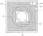
以上を踏まえ、以下では本発明の実施形態を図面を参照しながら説明する。図1は、本発明の一実施形態に係る非接触データキャリアの構成を模式的に示す平面図(図1(a))および垂直断面図(図1(b))である。図1に示すように、この非接触データキャリア50は、多層(4層)配線基板にアンテナパターン1、2、3、4を備え、このアンテナパターン1、2、3、4に接続してデータキャリア用のICチップ100が配線基板上に実装された概略構成を有する。配線基板にはほぼ中央にこの非接触データキャリア50を取り付け対象物(不図示)に取り付けるための貫通穴61がある。貫通穴61の空間を避けてアンテナパターン1、2、3、4が形成され、かつICチップ100が位置している。 Based on the above, embodiments of the present invention will be described below with reference to the drawings. FIG. 1 is a plan view (FIG. 1A) and a vertical sectional view (FIG. 1B) schematically showing the configuration of a non-contact data carrier according to an embodiment of the present invention. As shown in FIG. 1, this
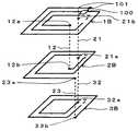
図2は、図1に示した非接触データキャリアにおけるアンテナの接続関係を示す模式的な分解斜視図である。図2において、図1中に示した構成要素と対応するものには同一の符号を付している。図1(b)から4つの配線層の各層に重畳的にアンテナパターン1、2、3、4が設けられることが、図2からは、これらのアンテナパターン1、2、3、4が所定に接続されることで、単一のアンテナパターンとなることが、それぞれ理解できる。 FIG. 2 is a schematic exploded perspective view showing an antenna connection relationship in the non-contact data carrier shown in FIG. 2, components corresponding to those shown in FIG. 1 are denoted by the same reference numerals. From FIG. 1B,
より具体的には、ICチップ100の機能面に形成されているパッドとアンテナパターン1の配線層とは、ボンディングワイヤ101で電気的に接続される。ワイヤボンディング101でICチップ100から接続されたアンテナパターン1の端部は渦巻き形状に形成されたアンテナパターン1の外周側端部である。この外周側端部からパターン1をたどりその内周側端部に設けられた層間接続用ランド(第1層)12aに至る。層間接続用ランド12aは、層間絶縁材51に設けられた1層2層間接続体12を介して層間接続用ランド(第2層)12bに電気的接続する。 More specifically, the pads formed on the functional surface of the
1層2層間接続体12には、例えばビアを用いることができるが、周知のスルーホール導電体を用いる構成も可能である(後述の2層3層間接続体23、32、3層4層間接続体34、43、1層2層間接続体21も同様である)。 For example, vias may be used for the first-layer / two-
層間接続用ランド(第2層)12bは、渦巻き形状に形成された内層(第2層)アンテナパターン2の内周側端部に設けられている。この内周側端部からパターン2をたどりその外周側端部に設けられた層間接続用ランド(第2層)23aに至る。層間接続用ランド23aは、層間絶縁材52に設けられた2層3層間接続体23を介して層間接続用ランド(第3層)23bに電気的接続する。 The interlayer connection land (second layer) 12b is provided at the inner peripheral side end of the inner layer (second layer)
層間接続用ランド(第3層)23bは、渦巻き形状に形成された内層(第3層)アンテナパターン3の外周側端部に設けられている。この外周側端部からパターン3をたどりその内周側端部に設けられた層間接続用ランド(第3層)34aに至る。層間接続用ランド34aは、層間絶縁材53に設けられた3層4層間接続体34を介して層間接続用ランド(第4層)34bに電気的接続する。 The interlayer connection land (third layer) 23 b is provided at the outer peripheral side end of the inner layer (third layer)
層間接続用ランド(第4層)34bは、渦巻き形状に形成された外層(第4層)アンテナパターン4の内周側端部に設けられている。この内周側端部からパターン4をたどりその外周側端部に設けられた層間接続用ランド(第4層)43aに至る。層間接続用ランド43aは、層間絶縁材53に設けられた3層4層間接続体43、第3層に設けられた層間接続用ランド32a、層間絶縁材52に設けられた2層3層間接続体32、第2層に設けられた層間接続用ランド21a、層間絶縁材51に設けられた1層2層間接続体21を介して層間接続用ランド(第1層)21bに電気的接続する。 The interlayer connection land (fourth layer) 34 b is provided at the inner peripheral end of the outer layer (fourth layer)
さらに、層間接続用ランド(第1層)21bを介して、ボンディングワイヤ101によりICチップ100で、配線として電気的接続が終端している。以上の構成によりアンテナパターン1、2、3、4は直列接続され、ICチップ100の単一のアンテナとして機能するようにされている。 Further, the electrical connection as a wiring is terminated in the
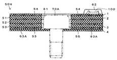
図1(b)に示すように、この非接触データキャリア100は、上記のアンテナパターン1、2、3、4、ICチップ100、層間接続用ランド12a、21b、12b、23a、21a、23b、34a、32a、34b、43a、1層2層間接続体12、21、2層3層間接続体23、32、3層4層間接続体34、43、層間絶縁材51、52、53とともに、ソルダーレジスト54、55、モールド樹脂(またはポッティング樹脂)62を有している。 As shown in FIG. 1B, the
アンテナパターン1、2、3、4を含む各配線層と、層間絶縁材51、52、53とは配線基板(サイズは例えば5mm角)を構成している。層間絶縁材51は、アンテナパターン1とアンテナパターン2とを隔てる絶縁基板であり、層間絶縁材52は、アンテナパターン2とアンテナパターン3とを隔てる絶縁基板であり、層間絶縁材53は、アンテナパターン3とアンテナパターン4とを隔てる絶縁基板である。 Each wiring layer including the
これらの層間絶縁材51、52、53はそれぞれ、例えばガラスクロス入りエポキシ系樹脂、アラミド樹脂、液晶ポリマー、またはBTレジンをその材料とすることができ、厚さは例えばそれぞれ例えば0.03mmないし0.1mmとすることができる。また、これらのリジッドな有機絶縁材料に代えて、ポリイミド、ポリエステル等のフレキシブルな有機絶縁材料の板材を用いることも可能である。さらにこれらの有機系材料の板材に代えて無機材料(セラミック)の板材を用いることも可能である。 Each of these
アンテナパターン1、2、3、4は、それぞれ、例えば銅箔をパターン形成したものであり、厚さは例えば18μmである。アンテナパターン1、2、3、4を形成するレイアウトルールとしてこの例では例えばライン/スペースが75μm/75μmのものを採用することができる。 Each of the
ICチップ100には、主たる内部構成要素として、通信回路部(不図示)とメモリ部(不図示)とが設けられている。通信回路部は、アンテナパターン1、2、3、4により構成されるアンテナに接続され、このアンテナを介して外部からのデータ読み出し指令信号を受信しかつこれに反応してメモリ部に格納されたデータの出力の仲介を行う。 The
ソルダーレジスト54は、外層(第1層)アンテナパターン1が設けられた層間絶縁材51の面に、はんだ接続の必要のないパターン部位上を含んで形成されている(厚さは例えば25μm:図1(a)では図示省略)。ソルダーレジスト55は、外層(第4層)アンテナパターン4が設けられた層間絶縁材53の面に、はんだ接続の必要のないパターン部位上を含んで形成されている(厚さはソルダーレジスト54と同様に例えば25μm)。 The solder resist 54 is formed on the surface of the
モールド樹脂62は、少なくとも、層間絶縁材51の面上に機能面を上に向けて設けられたICチップ100を覆うように、この場合島状樹脂層として形成されている(厚さは例えば0.5mm)。モールド樹脂62の材質は、例えばエポキシ樹脂とすることができる。モールド樹脂62によりICチップ100は、外部環境から化学的・物理的に保護される。モールド樹脂62は、例えばトランスファーモールドにより成型して形成できるが、これに代えて、液状またはペースト状樹脂のポッティングによりICチップ100を覆うようにポッティング樹脂として形成することもできる。 In this case, the
この非接触データキャリア50の製造工程の概略は、例えば以下である。まず、銅箔の必要な位置に層間接続のため(2層3層間接続体23、32のため)の突起状の銀ペーストバンプを印刷形成し、その銀ペーストバンプが貫通するようにその銅箔上に層間絶縁材52を積層一体化する。次に、貫通した銀ペーストの先端を塑性変形するように層間絶縁材52上に別の銅箔を積層一体化する。そして、両面の銅箔をエッチングでパターン化しアンテナパターン2、3を含む配線パターンとする。 The outline of the manufacturing process of the
次に、さらに別の銅箔の必要な位置に層間接続のため(1層2層間接続体12、21、または3層4層間接続体34、43のため)の突起状の銀ペーストバンプが形成され、その銀ペーストバンプが貫通するようにそれらの銅箔上に層間絶縁材51または53が積層一体化されたものを用意する。そして、これらを上記のアンテナパターン2、3が形成された層間絶縁材52上両面に、それらの貫通した銀ペーストの先端を塑性変形させるようにそれぞれ積層一体化する。次いで、層間絶縁材51上の銅箔、層間絶縁材53上の銅箔をそれぞれエッチングでパターン化しアンテナパターン1、4を含む配線パターンを形成する。以下、ソルダーレジスト54、55の形成、貫通穴61の形成(例えばドリリングによる)、金めっき処理、ICチップ100の実装、モールド樹脂62の形成の各工程を順に行う。この場合、各層間接続体は銀ペースト硬化導電樹脂からなる。 Next, protruding silver paste bumps are formed at the required positions of another copper foil for the purpose of interlayer connection (for the
図1、図2に示す実施形態では、層間絶縁材51等からなる配線基板が矩形状であり、ICチップ100はそのひとつの隅付近に実装されている。このICチップ100の位置を避けて外層アンテナパターン1が形成されている(他のアンテナパターン2、3、4はICチップ100の位置に重なりがあってもよい(図2参照)。)。このような隅へのICチップ100の実装位置によれば、アンテナパターン1の形成領域の確保上都合がよい。すなわちこの結果、アンテナパターン1の開口面積の減少はわずかで済み、したがって、より小型の基板面積で良好な通信特性を得ることができる。 In the embodiment shown in FIGS. 1 and 2, the wiring substrate made of the
また、貫通穴61の形成位置を配線基板のほぼ中央としているので、アンテナパターン1、2、3、4の形成位置との互いのバッティングがなく、貫通穴61を備えた上で非接触データキャリア50として小型化が実現されている。なお、貫通穴61の平面形状は、図示するような円形のほか、多角形や離心率のあまり大きくない楕円などとしてもよい。 In addition, since the formation position of the through
図3は、図1に示した非接触データキャリアを取り付け対象物に取り付けた状態(一例)を示す垂直断面図である。図3において、すでに説明した図中に登場した構成要素と同一または同一相当のものには同一符号を付している。その部分の説明は省略する。 FIG. 3 is a vertical cross-sectional view showing a state (one example) in which the non-contact data carrier shown in FIG. 1 is attached to an attachment target. In FIG. 3, the same reference numerals are given to the same or equivalent components as those shown in the already described drawings. The description of that part is omitted.
図3に示すように、上記説明の非接触データキャリア50は、取り付け部材としてのねじ70を用いその軸部70bを貫通穴61に挿通させて、取り付け対象物80に取り付け、固定することができる。このようなねじ70を用いた締結を利用すればその取り付け強度を増すことができ取り付けの信頼性を向上できる。取り付け対象物80には、例えば、あらかじめ内壁にめねじの形成された取り付け穴80aを設けておく。ねじの種類によってはあらかじめの取り付け穴80aの形成が不要の場合もあり得る。 As shown in FIG. 3, the
取り付け部材には、ねじのほか、一般には、軸部70bに相当する挿通部と貫通穴61に挿通できない形状の非挿通部(ねじの頭部70aに相当)とを備えたものを用いることができる。取り付け部材は、また、非導電性材料(例えば樹脂)とすると好ましい。これは、アンテナパターン1、2、3、4との距離が近くなるので、その通信性能に悪影響を与えるのを避けるためである。 In addition to the screw, the attachment member generally includes an insertion portion corresponding to the
図4は、図1に示した非接触データキャリアを取り付け対象物に取り付けた状態(別の例)を示す垂直断面図である。図4において、すでに説明した図中に登場した構成要素と同一または同一相当のものには同一符号を付している。その部分の説明は省略する。 FIG. 4 is a vertical sectional view showing a state (another example) in which the non-contact data carrier shown in FIG. 1 is attached to an attachment target. In FIG. 4, the same reference numerals are given to the same or equivalent components as those shown in the already described drawings. The description of that part is omitted.
この例では、取り付け部材として、ねじに代えて頭部71a、軸部71bを有する非導電性材料のリベット71を用いている。すなわち、取り付け対象物80に設けられた取り付け穴80bに対してリベット71の軸部71bをしまりばめすることにより非接触データキャリア50を固定する。取り付け部材、取り付け対象物80ともにねじ部がなく、より構成を単純化できる。 In this example, a
次に、本発明の別の実施形態について図5を参照して説明する。図5は、本発明の別の実施形態に係る非接触データキャリアの構成を模式的に示す平面図である。図5において、すでに説明した図中に登場した構成要素と同一または同一相当のものには同一符号を付している。その部分の説明は省略する。 Next, another embodiment of the present invention will be described with reference to FIG. FIG. 5 is a plan view schematically showing a configuration of a non-contact data carrier according to another embodiment of the present invention. In FIG. 5, the same reference numerals are given to the same or equivalent components as those shown in the already described drawings. The description of that part is omitted.
この実施形態の非接触データキャリア50Aと図1、図2に示した非接触データキャリア50との違いは、ボンディングワイヤにより実装がされたICチップ100に代えてフリップチップ接続により実装がされたICチップ100Aを用いている点である。フリップチップ接続のためアンテナパターン1の形成された配線層のパターンがICチップ100Aの周りで図1に示す場合と多少異なるが、他の部分は同一である。このようにフリップチップ接続によるICチップ100Aの実装であっても、上記実施形態の特徴は維持される。 The difference between the
フリップチップ接続は、例えば、ICチップ100Aの機能面上に突起電極を設け、この突起電極を介して第1層アンテナパターン1が存する外層配線層にICチップ100Aを固定するようにして行う。ICチップ100Aの機能面と層間絶縁材51との間には、ICチップ100Aと外層配線層との接続部位を外部環境から化学的、物理的に保護するため、アンダーフィル樹脂を充填するのが好ましい。このようなアンダーフィル樹脂の形成のため、ICチップ100Aと外層配線層との間にあらかじめ異方性導電樹脂や非導電樹脂を充填するような接続方法を用いることができる。さらにフリップチップ接続されたICチップ100Aを覆うようにモールド樹脂(またはポッティング樹脂)を形成するようにしてもよい(図1参照)。 The flip chip connection is performed, for example, by providing a protruding electrode on the functional surface of the
次に、本発明のさらに別の実施形態について図6を参照して説明する。図6は、本発明のさらに別の実施形態に係る非接触データキャリアの構成を模式的に示す垂直断面図である。図6において、すでに説明した図中に登場した構成要素と同一または同一相当のものには同一符号を付している。その部分の説明は省略する。 Next, still another embodiment of the present invention will be described with reference to FIG. FIG. 6 is a vertical sectional view schematically showing a configuration of a non-contact data carrier according to still another embodiment of the present invention. In FIG. 6, the same reference numerals are given to the same or equivalent components as those shown in the already described drawings. The description of that part is omitted.
この実施形態の非接触データキャリア50Bと図1、図2に示した非接触データキャリア50との違いは、島状に形成されたモールド樹脂62に代えて、配線基板の主面上全面(貫通穴61に連なる貫通があるのは配線基板と共通)に封止樹脂62Aを形成している点である。当然ながら封止樹脂62AによりICチップ100は封止されている。 The difference between the
封止樹脂62Aが配線基板の主面上全面に形成されていることで、取り付け部材としてのねじ70の頭部70aは、封止樹脂62Aの層に接触することになる。他の部分の構成は図1、図2に示した非接触データキャリア50と同一である。ねじ70の頭部70aが直接的には封止樹脂62Aに接触するので、外層アンテナパターン1への圧迫やせん断の作用が低下し、アンテナパターン1が破壊されるのを回避する上で好ましい。また、配線基板の主面上全面への封止樹脂62Aの形成は、モールド樹脂62(図1)の形成より容易であり低コスト化が見込める。さらに、ねじ70の頭部70aが島状のモールド樹脂62(図1)の位置に干渉することがないので配線基板がより小型の場合にも向いている。 Since the sealing
次に、本発明のさらに別の実施形態について図7を参照して説明する。図7は、本発明のさらに別の実施形態に係る非接触データキャリアの構成を模式的に示す垂直断面図である。図7において、すでに説明した図中に登場した構成要素と同一または同一相当のものには同一符号を付している。その部分の説明は省略する。 Next, still another embodiment of the present invention will be described with reference to FIG. FIG. 7 is a vertical sectional view schematically showing a configuration of a non-contact data carrier according to still another embodiment of the present invention. In FIG. 7, the same reference numerals are given to the same or equivalent components as those shown in the already described drawings. The description of that part is omitted.
この実施形態の非接触データキャリア50Cは、上記の非接触データキャリア50Bと似ているが、配線基板の主面上全面に形成された封止樹脂62Aに代えて、配線基板の貫通穴61より大きな横断面積を有して貫通部を有する封止樹脂62Bを備える点で異なる。当然ながら封止樹脂62BによりICチップ100は封止されている。 The non-contact data carrier 50C of this embodiment is similar to the
この実施形態の場合、封止樹脂62Bの貫通部にねじ70の頭部70aを落ち込ませて位置させることができる。見方を変えると、図6に示した非接触データキャリア50Bに比較して配線基板が比較的大きい場合に採り得る態様である。また、封止樹脂62Bの厚みの分だけ取り付け状態における全高を抑制できる効果がある。 In the case of this embodiment, the head portion 70a of the
次に、本発明のさらに別の実施形態について図8を参照して説明する。図8は、本発明のさらに別の実施形態に係る非接触データキャリアの構成を模式的に示す平面図(図8(a))および垂直断面図(図8(b))である。図8において、すでに説明した図中に登場した構成要素と同一または同一相当のものには同一符号を付している。その部分の説明は省略する。 Next, still another embodiment of the present invention will be described with reference to FIG. FIG. 8 is a plan view (FIG. 8A) and a vertical sectional view (FIG. 8B) schematically showing the configuration of a non-contact data carrier according to still another embodiment of the present invention. In FIG. 8, the same reference numerals are given to the same or equivalent components as those shown in the already described drawings. The description of that part is omitted.
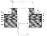
この実施形態の非接触データキャリア50Dと図1、図2に示した非接触データキャリア50との違いは、外層(第1層)アンテナパターン1に代えて、ねじ70の頭部70aとの重なりに相当する領域を避けて外層(第1層)アンテナパターン1Aが形成されている点である。このため層間接続用ランド12aの位置がより外周寄りになり、これに伴い内層(第2層)アンテナパターン2Aも内周側での形成領域がなくなっている(図8(b)参照)。他の部分は同一である。この実施形態では、ねじ70の頭部70aによる外層アンテナパターン1Aへの圧迫やせん断の作用の発生がなくなり、アンテナパターン1Aが破壊されるのを回避する上でより好ましい。 The difference between the
次に、本発明のさらに別の実施形態について図9を参照して説明する。図9は、本発明のさらに別の実施形態に係る非接触データキャリアの構成を模式的に示す平面図(図9(a))および垂直断面図(図9(b))である。図9において、すでに説明した図中に登場した構成要素と同一または同一相当のものには同一符号を付している。その部分の説明は省略する。 Next, still another embodiment of the present invention will be described with reference to FIG. FIG. 9 is a plan view (FIG. 9A) and a vertical sectional view (FIG. 9B) schematically showing the configuration of a non-contact data carrier according to still another embodiment of the present invention. In FIG. 9, the same reference numerals are given to the same or equivalent components as those already described in the drawings. The description of that part is omitted.
この実施形態の非接触データキャリア50Eと図6(この実施形態は図6に示した実施形態がより参考になる)に示した非接触データキャリア50Bとの違いは、4層からなるアンテナパターン1、2、3、4を有する配線基板に代えて3層のアンテナパターン1B、2B、3Bを有する配線基板を用いている点である。このため、ICチップ100からのボンディングワイヤ101が外層(第1層)アンテナパターン1Bの内周側と外周側とにそれぞれ接続されている。ICチップ100がアンテナパターン1Bに重なるが、ソルダーレジスト54(または別の非導電性の接着層)を介して重ねるようすればアンテナとしての機能を損なわず、ICチップ100の動作も損なわれない。 The difference between the
図10は、図9に示した非接触データキャリア50Eにおけるアンテナの接続関係を示す模式的な分解斜視図である。図10において、図9中に示した構成要素と対応するものには同一の符号を付しており、さらにすでに説明した図中に登場の構成要素と対応するものにも同一の符号を付している。図9(b)から3つの配線層の各層に重畳的にアンテナパターン1B、2B、3Bが設けられることが、図10からは、これらのアンテナパターン1B、2B、3Bが所定に接続されることで、単一のアンテナパターンとなることが、それぞれわかる。より具体的な説明は、すでに行った図2を参照する説明と同趣旨なので省略する。 FIG. 10 is a schematic exploded perspective view showing an antenna connection relationship in the
この実施形態では、すべての配線層においてアンテナパターンの形成がICチップ100の位置を退避せずに可能であり、大きなアンテナパターンの開口面積を得ることができる。したがって、より小型の基板面積で良好な通信特性を得ることができる。これは、ねじ70の頭部70aが島状のモールド樹脂62(図1)の位置に干渉することがない点も寄与している。 In this embodiment, antenna patterns can be formed in all wiring layers without retracting the position of the
次に、本発明のさらに別の実施形態について図11を参照して説明する。図11は、本発明のさらに別の実施形態に係る非接触データキャリアの構成を模式的に示す垂直断面図である。図11において、すでに説明した図中に登場した構成要素と同一または同一相当のものには同一符号を付している。その部分の説明は省略する。 Next, still another embodiment of the present invention will be described with reference to FIG. FIG. 11 is a vertical sectional view schematically showing a configuration of a non-contact data carrier according to still another embodiment of the present invention. In FIG. 11, the same reference numerals are given to the same or equivalent components as those shown in the already described drawings. The description of that part is omitted.
この実施形態の非接触データキャリア50Fと図8(この実施形態は図8に示した実施形態がより参考になる)に示した非接触データキャリア50Dとの違いは、ねじ70の頭部70a側の層間絶縁材51に代えて、この頭部70aを落ち込ませて位置させるようにキャビティを有する層間絶縁材51Aを用いている点である。その他の点は同一である。キャビティの存在により、貫通穴61は、より小さな横断面積を有する部分とより大きな横断面積を有する部分との結合になる。このようなキャビティを設けるには、少なくともこのキャビティに相当の位置に外層(第1層)アンテナパターンがもともとないことが条件になる。この点で図8に示した形態は向いている。 The difference between the
なお、一般には、キャビティの底にアンテナパターンが在る場合であってもよい。そのアンテナパターン上にソルダーレジスト54と同様な層を形成すれば、ねじ70の頭部70aとの接触関係は例えば図3に示した態様と同じになる。図11に示す実施形態によれば、取り付け対象物に取り付けられた場合の高さ方向のサイズを抑制することができる。 In general, an antenna pattern may be present at the bottom of the cavity. If a layer similar to the solder resist 54 is formed on the antenna pattern, the contact relationship with the head 70a of the
次に、本発明のさらに別の実施形態について図12を参照して説明する。図12は、本発明のさらに別の実施形態に係る非接触データキャリアの構成を模式的に示す垂直断面図である。図12において、すでに説明した図中に登場した構成要素と同一または同一相当のものには同一符号を付している。その部分の説明は省略する。 Next, still another embodiment of the present invention will be described with reference to FIG. FIG. 12 is a vertical sectional view schematically showing a configuration of a non-contact data carrier according to still another embodiment of the present invention. In FIG. 12, the same reference numerals are given to the same or equivalent components as those already described in the drawings. The description of that part is omitted.
この実施形態の非接触データキャリア50Gと図1、図2に示した非接触データキャリア50との違いは、配線基板の一方の主面上に接着層(または粘着層)63をさらに設けた点である。その他の点は同一である。接着層63は、貫通穴61に連続して貫通している。接着層63を備えることで、接着により(粘着層の場合は粘着により)この非接触データキャリア50Gを取り付け対象物に固定することができる。そして必要なら、貫通穴61を利用してすでに説明したような取り付け部材を用いて補強固定を行うことができる。 The difference between the
接着層(または粘着層)63には各種公知のものを利用することができる。例えば、1層構造の接着材層(または粘着材層)からなるもの、接着材層(粘着材層)と樹脂基材層とからなる2層構造のもの、接着材層(粘着材層)と樹脂基材層と接着材層(粘着材層)とからなる3層構造のものなどである。接着材層にはアクリル系、エポキシ系、シリコン系などがあり、樹脂基材層にはPET、PE、PP、フェノール、PIなどがある。 Various known materials can be used for the adhesive layer (or adhesive layer) 63. For example, an adhesive layer (or adhesive layer) having a single layer structure, a two-layer structure including an adhesive layer (adhesive layer) and a resin base layer, an adhesive layer (adhesive layer), and A three-layer structure composed of a resin base material layer and an adhesive material layer (adhesive material layer). The adhesive layer includes acrylic, epoxy, and silicon types, and the resin base layer includes PET, PE, PP, phenol, PI, and the like.
次に、本発明のさらに別の実施形態について図13を参照して説明する。図13は、本発明のさらに別の実施形態に係る非接触データキャリアの構成を模式的に示す垂直断面図である。図13において、すでに説明した図中に登場した構成要素と同一または同一相当のものには同一符号を付している。その部分の説明は省略する。 Next, still another embodiment of the present invention will be described with reference to FIG. FIG. 13 is a vertical sectional view schematically showing a configuration of a non-contact data carrier according to still another embodiment of the present invention. In FIG. 13, the same reference numerals are given to the same or equivalent components as those shown in the already described drawings. The description of that part is omitted.
この実施形態の非接触データキャリア50Hと図12(この実施形態は図12に示した実施形態がより参考になる)に示した非接触データキャリア50Gとの違いは、接着層63に代えて、配線基板の貫通穴61にのぞく空間に延長部分がある接着層(または粘着層)63Aを設けた点である。その他の部分は同一である。 The difference between the
このような態様によれば、図示するように、取り付け部材としてのねじ70Aをその頭部が貫通穴61内に埋没するように位置させることができる。この結果、ねじ70Aの頭部により接着層63Aが押圧される状態になる。貫通穴16に埋没できる取り付け部材(ねじ70A)を用いることで、取り付け対象物に取り付けられた場合の高さ方向のサイズを抑制することができる。 According to such an aspect, as shown in the figure, the
次に、本発明のさらに別の実施形態について図14を参照して説明する。図14は、本発明のさらに別の実施形態に係る非接触データキャリアの構成を模式的に示す垂直断面図である。図14において、すでに説明した図中に登場した構成要素と同一または同一相当のものには同一符号を付している。その部分の説明は省略する。 Next, still another embodiment of the present invention will be described with reference to FIG. FIG. 14 is a vertical sectional view schematically showing a configuration of a non-contact data carrier according to still another embodiment of the present invention. In FIG. 14, the same reference numerals are given to the same or equivalent components as those shown in the already described drawings. The description of that part is omitted.
この実施形態の非接触データキャリアは、図1、図2で説明した非接触データキャリア50を用い、さらにその配線基板の一方の主面に非導電性材料のスペーサ層64を付加した形態である。スペーサ層64は、この形態ではICチップ100の実装された側とは反対側に設けられ、また、配線基板の貫通穴61に延長して貫通した形状である。このような貫通により、取り付け状態における機械的な安定性(よって姿勢安定により通信の安定性)がより向上する。 The non-contact data carrier of this embodiment uses the
スペーサ層64を設けることの主要な目的は、取り付け対象物とアンテナパターン1、2、3、4との間の距離をある程度確保するためである。これによれば、例えば取り付け対象物が金属のような導電性材料の場合にも、通信性能への悪影響を抑制できる。実験によると、取り付け対象物からアンテナパターン4までの距離が2mm以上になるようにスペーサ層64を設けると好ましい。 The main purpose of providing the
次に、本発明のさらに別の実施形態について図15を参照して説明する。図15は、本発明のさらに別の実施形態に係る非接触データキャリアの構成を模式的に示す垂直断面図である。図15において、すでに説明した図中に登場した構成要素と同一または同一相当のものには同一符号を付している。その部分の説明は省略する。 Next, still another embodiment of the present invention will be described with reference to FIG. FIG. 15 is a vertical sectional view schematically showing a configuration of a non-contact data carrier according to still another embodiment of the present invention. In FIG. 15, the same reference numerals are given to the same or equivalent components as those shown in the already described drawings. The description of that part is omitted.
この実施形態の非接触データキャリアは、上記の図14で説明した形態の非接触データキャリアに対して、さらに、スペーサ層64の配線基板とは反対側に接着層(または粘着層)63を設けたものである。接着層(または粘着層)63については、すでに図12などで説明した通りの構成、作用、効果になる。 In the non-contact data carrier of this embodiment, an adhesive layer (or adhesive layer) 63 is further provided on the side opposite to the wiring substrate of the
次に、本発明のさらに別の実施形態について図16を参照して説明する。図16は、本発明のさらに別の実施形態に係る非接触データキャリアの構成を模式的に示す垂直断面図である。図16において、すでに説明した図中に登場した構成要素と同一または同一相当のものには同一符号を付している。その部分の説明は省略する。 Next, still another embodiment of the present invention will be described with reference to FIG. FIG. 16 is a vertical sectional view schematically showing a configuration of a non-contact data carrier according to still another embodiment of the present invention. In FIG. 16, the same reference numerals are given to the same or equivalent components as those shown in the already described drawings. The description of that part is omitted.
この実施形態の非接触データキャリアは、図14(この実施形態は図12に示した実施形態がより参考になる)に示した非接触データキャリアと比較して、スペーサ層64の配置位置が配線基板に対してその反対側になっている点で異なる。その他の部分は同一である。すなわち、スペーサ層64は、島状のモールド樹脂62による配線基板上の凸形状を吸収する相補形状となっている。 Compared with the non-contact data carrier shown in FIG. 14 (the embodiment shown in FIG. 12 is more useful as a reference), the non-contact data carrier of this embodiment has a wiring position of the
これにより、全体としての形状がまとまるのみならず、取り付け部材としてのねじ70の頭部径が大きい場合であっても、その頭部がモールド樹脂62の凸形状に干渉することがなくなる。したがって、相対的に配線基板がさらに小さい場合にも向いている。 Thereby, not only the shape as a whole is gathered, but even if the head diameter of the
次に、本発明のさらに別の実施形態について図17を参照して説明する。図17は、本発明のさらに別の実施形態に係る非接触データキャリアの構成を模式的に示す垂直断面図である。図17において、すでに説明した図中に登場した構成要素と同一または同一相当のものには同一符号を付している。その部分の説明は省略する。 Next, still another embodiment of the present invention will be described with reference to FIG. FIG. 17 is a vertical sectional view schematically showing a configuration of a non-contact data carrier according to still another embodiment of the present invention. In FIG. 17, the same reference numerals are given to the same or equivalent components as those shown in the already described drawings. The description of that part is omitted.
この実施形態の非接触データキャリアは、図16(この実施形態は図16に示した実施形態がより参考になる)に示した非接触データキャリアと比較して、スペーサ層64に持たせていた、島状のモールド樹脂62の凸形状を吸収する機能を、ある程度硬質のスポンジなどからなる緩衝層65に持たせた点で異なる。その他の部分は同一である。スペーサ層64と緩衝層65とでアンテナパターンと取り付け対象物との距離を所定に確保する。 The non-contact data carrier of this embodiment is provided in the
緩衝層65を設けることで、島状のモールド樹脂62による配線基板上の凸形状を吸収する態様は容易に実現される。すなわち、スペーサ層65によって凸形状を吸収するには、例えば樹脂成型などの工程を用いてスペーサ層65を形成する必要があるが、緩衝層65によればこのような工程を要しない。 By providing the buffer layer 65, an aspect of absorbing the convex shape on the wiring board by the island-shaped
次に、本発明のさらに別の実施形態について図18を参照して説明する。図18は、本発明のさらに別の実施形態に係る非接触データキャリアの構成を模式的に示す垂直断面図である。図18において、すでに説明した図中に登場した構成要素と同一または同一相当のものには同一符号を付している。その部分の説明は省略する。 Next, still another embodiment of the present invention will be described with reference to FIG. FIG. 18 is a vertical sectional view schematically showing a configuration of a non-contact data carrier according to still another embodiment of the present invention. In FIG. 18, the same reference numerals are given to the same or equivalent components as those shown in the already described drawings. The description of that part is omitted.
この実施形態の非接触データキャリアは、図14(この実施形態は図14に示した実施形態がより参考になる)に示した非接触データキャリアと比較して、スペーサ層64が設けられた側とは反対の配線基板上にもスペーサ層66が設けられた点で異なる。その他の部分は同一である。第2のスペーサ層66を設けることで、取り付け部材としてのねじ70B(特にその頭部)とアンテナパターン1との距離をある程度確保することを目的とする。このような距離の確保により、例えばねじ70Bが金属などの導電性部材であっても通信性能に対する悪影響を抑制することができる。 Compared with the non-contact data carrier shown in FIG. 14 (the embodiment shown in FIG. 14 is more helpful), the non-contact data carrier of this embodiment is the side on which the
次に、本発明のさらに別の実施形態について図19を参照して説明する。図19は、本発明のさらに別の実施形態に係る非接触データキャリアの構成を模式的に示す垂直断面図である。図19において、すでに説明した図中に登場した構成要素と同一または同一相当のものには同一符号を付している。その部分の説明は省略する。 Next, still another embodiment of the present invention will be described with reference to FIG. FIG. 19 is a vertical sectional view schematically showing a configuration of a non-contact data carrier according to still another embodiment of the present invention. In FIG. 19, the same reference numerals are given to the same or equivalent components as those shown in the already described drawings. The description of that part is omitted.
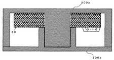
この実施形態の非接触データキャリアは、図1、図2で説明した非接触データキャリア50を用い、その取り付け部材として図示するような容器状の形状を有するものを利用する。すなわち、配線基板の貫通穴に挿通可能な突起を有する一方の側の容器状取り付け部材200aと、この突起をはめ込み可能な凹部を有する他方の側の容器状取り付け部材200bとにより、非接触データキャリア50を挟み固定する。図示する取り付け部材200aの上面、または取り付け部材200bの下面が取り付け対象物に固定される。このような容器状取り付け部材200a、200bを用いれば取り付け対象の側に特別な加工を要しない。また、非接触データキャリア50の保護性が向上する。 As the non-contact data carrier of this embodiment, the
次に、本発明のさらに別の実施形態について図20を参照して説明する。図20は、本発明のさらに別の実施形態に係る非接触データキャリアの構成を模式的に示す垂直断面図である。図20において、すでに説明した図中に登場した構成要素と同一または同一相当のものには同一符号を付している。その部分の説明は省略する。 Next, still another embodiment of the present invention will be described with reference to FIG. FIG. 20 is a vertical sectional view schematically showing a configuration of a non-contact data carrier according to still another embodiment of the present invention. In FIG. 20, the same reference numerals are given to the same or equivalent components as those already shown in the drawings. The description of that part is omitted.
この実施形態の非接触データキャリアは、取り付け部材として容器状のものを用いる点で上記の図19に示したものと同じであるが、さらに、容器状取り付け部材300と非接触データキャリア50との間に隙間がなく密着している点で異なる。このような態様は、例えば、非接触データキャリア50を金型中に存在させた樹脂成型を用いれば実現可能である。図示する取り付け部材300の上面または下面が取り付け対象物に固定される。このような容器状取り付け部材300を用いれば取り付け対象の側に特別な加工を要しない。 The non-contact data carrier of this embodiment is the same as that shown in FIG. 19 above in that a container-like one is used as an attachment member, but further, the container-
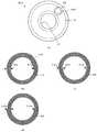
次に、本発明のさらに別の実施形態について図21を参照して説明する。図21は、本発明のさらに別の実施形態に係る非接触データキャリアの構成を模式的に示す平面図(図21(a))、およびその各層のアンテナパターンを示す4つの平面図(図21(b)〜(d))である。図21において、すでに説明した図中に登場した構成要素と同一または同一相当のものには同一符号を付している。その部分の説明は省略する。 Next, still another embodiment of the present invention will be described with reference to FIG. FIG. 21 is a plan view schematically showing a configuration of a non-contact data carrier according to still another embodiment of the present invention (FIG. 21A), and four plan views showing antenna patterns of each layer (FIG. 21). (B) to (d)). In FIG. 21, the same reference numerals are given to the same or equivalent components as those shown in the already described drawings. The description of that part is omitted.
この実施形態の上記説明の各実施形態との大きな違いは、配線基板の平面形状がほぼ円形(直径は例えば10mm)になっていることである。すなわち、この非接触データキャリア50Iは、図1、図2と同様な4層配線基板を有するが全体として円形状であり、そのほぼ中央に、取り付け用の貫通穴61が設けられている。円形状とすることで、矩形状の配線基板に比較して配線基板の母材からの切り出し時に使用できない領域が発生する。しかしながら、非接触データキャリアとしての用途によってはこのような形状が求められる場合がある。このような円形状の配線基板は、切り出し前の母材において、まわりの母材との間に分離用の円弧状スリットを設けておくことにより形成できる。 The major difference between this embodiment and each of the embodiments described above is that the planar shape of the wiring board is substantially circular (diameter is, for example, 10 mm). That is, the non-contact data carrier 50I has a four-layer wiring board similar to that shown in FIGS. 1 and 2, but has a circular shape as a whole, and a through
アンテナパターンについては、第1層アンテナパターン1Cは主として他の配線層のアンテナパターン2C、3C、4Cとの接続を行うために、アンテナとしては省略されたパターンを有する。外層配線層としてのアンテナパターン1CとICチップ100とは重なりがない配置である。図21(b)〜(d)において使用した各符号は、図2において使用した符号にそれぞれ対応している。これらの符号を追うことにより、アンテナパターン1C、2C、3C、4Cが所定に接続され、単一のアンテナパターンとなることが理解できる。 As for the antenna pattern, the first-layer antenna pattern 1C has a pattern omitted as an antenna mainly for connection with the
このような円形状の配線基板を有する非接触データキャリア50Iにおいても、そのほぼ中央に貫通穴61を有することで、貫通穴61を備えた上で非接触データキャリア50Iとして小型化が実現されている。 Even in the non-contact data carrier 50I having such a circular wiring board, the through-
次に、本発明のさらに別の実施形態について図22を参照して説明する。図22は、本発明のさらに別の実施形態に係る非接触データキャリアの構成を模式的に示す平面図(図22(a))、およびその各層のアンテナパターンを示す3つの平面図(図22(b)〜(d))である。図22において、すでに説明した図中に登場した構成要素と同一または同一相当のものには同一符号を付している。その部分の説明は省略する。 Next, still another embodiment of the present invention will be described with reference to FIG. FIG. 22 is a plan view schematically showing the configuration of a non-contact data carrier according to still another embodiment of the present invention (FIG. 22A), and three plan views showing antenna patterns of each layer (FIG. 22). (B) to (d)). In FIG. 22, the same reference numerals are given to the same or equivalent components as those already described in the drawings. The description of that part is omitted.
この実施形態の非接触データキャリア50Jと上記図21に示した非接触データキャリア50Iとの違いは、4層からなるアンテナパターン1C、2C、3C、4Cを有する配線基板に代えて3層のアンテナパターン1D、2D、3Dを有する配線基板を用いている点である。このため、ICチップ100がアンテナパターン1Dに重なるように配置されている。これらの点は図9で説明した実施形態と共通する。ICチップ100とアンテナパターン1Dとの間は、ソルダーレジスト(または別の非導電性の接着層)を介して重ねるようすればアンテナとしての機能を損なわず、ICチップ100の動作も損なわれない。 The
以上、本発明の実施形態を複数説明したが、各実施形態の特徴部分を適宜組み合わせてさらに別の実施形態とすることは、上記各開示内容から容易に可能である。例えば円形状の配線基板の場合であっても、図3、図4に挙げた取り付け部材の変形例、図5で説明したICのフリップリチップ接続、図6、図7に挙げた封止樹脂62A、62Bの採用、…等々明らかに可能である。また、例えば、図6、図7に挙げた封止樹脂62A、62Bの採用を図14、図15、図16などのスペーサ層64を有する実施形態で図ることも可能である。同様に考えてさらに種々の実施形態を生み出すことができる。 As described above, a plurality of embodiments of the present invention have been described. However, it is possible to easily combine the characteristic portions of each embodiment into another embodiment from the above disclosure. For example, even in the case of a circular wiring board, a modification of the mounting member shown in FIGS. 3 and 4, flip-chip connection of the IC described in FIG. 5, and the sealing resin shown in FIGS. 6 and 7 It is clearly possible to adopt 62A, 62B, and so on. Further, for example, it is possible to adopt the sealing
1,1A,1B,1C,1D…第1層(外層)アンテナパターン、2,2A,2B,2C,2D…第2層(内層)アンテナパターン、3,3B,3C,3D…第3層アンテナパターン、4,4C…第4層(外層)アンテナパターン、12,21…1層2層間接続体、23,32…2層3層間接続体、34,43…3層4層間接続体、12a,21b…層間接続用ランド(第1層)、12b,21a,23a…層間接続用ランド(第2層)、23b,32a,34a…層間接続用ランド(第3層)、34b,43a…層間接続用ランド(第4層)、50,50A,50B,50C,50D,50E,50F,50G,50H,50I,50J…非接触データキャリア、51,51A,52,53…層間絶縁材、54,55…ソルダーレジスト、61…貫通穴、62…モールド樹脂(またはポッティング樹脂)、62A,62B…封止樹脂、63,63A…接着層(または粘着層)、64…スペーサ層、65…緩衝層、66…スペーサ層、70,70A…ねじ、70B…ねじ(導電性)、70a…頭部、70b…軸部、71…リベット、71a…頭部、71b…軸部、80…取り付け対象物、80a…取り付け穴(めねじあり)、80b…取り付け穴、100…ICチップ、101…ボンディングワイヤ、200a,200b…容器状取り付け部材、300…成型樹脂製取り付け部材。 1, 1A, 1B, 1C, 1D ... first layer (outer layer) antenna pattern, 2, 2A, 2B, 2C, 2D ... second layer (inner layer) antenna pattern, 3, 3B, 3C, 3D ... third layer antenna Pattern, 4, 4C ... 4th layer (outer layer) antenna pattern, 12, 21 ... 1
Claims (24)
Translated fromJapanese前記配線基板に実装されかつ前記アンテナパターンに電気的に接続された、データを格納可能なICチップと
を具備することを特徴とする非接触データキャリア。A wiring board provided with an antenna pattern and having a through hole at substantially the center;
An IC chip mounted on the wiring board and electrically connected to the antenna pattern and capable of storing data.
前記ICチップが、前記配線基板のひとつの隅近辺に実装され、
前記配線基板の前記アンテナパターンが、少なくとも外層配線パターンとして形成されており、該外層配線パターンとしてのアンテナパターンが、前記実装されたICチップの位置を退避して形成されていること
を特徴とする請求項1記載の非接触データキャリア。The wiring board is substantially rectangular;
The IC chip is mounted near one corner of the wiring board,
The antenna pattern of the wiring board is formed as at least an outer layer wiring pattern, and the antenna pattern as the outer layer wiring pattern is formed by retracting the position of the mounted IC chip. The contactless data carrier according to claim 1.
前記ICチップが、前記外層配線パターンとしてのアンテナパターンに重なりを有して実装されていること
を特徴とする請求項1記載の非接触データキャリア。The antenna pattern of the wiring board is formed as at least an outer layer wiring pattern,
The non-contact data carrier according to claim 1, wherein the IC chip is mounted so as to overlap an antenna pattern as the outer layer wiring pattern.
前記実装されたICチップを覆うように前記配線基板の前記一方の主面上に設けられた樹脂層をさらに具備し、
前記樹脂層が、前記配線基板が有する前記貫通穴に延長して貫通していること
を特徴とする請求項1記載の非接触データキャリア。The IC chip is mounted on one main surface of the wiring board,
A resin layer provided on the one main surface of the wiring board so as to cover the mounted IC chip;
The non-contact data carrier according to claim 1, wherein the resin layer extends through the through hole of the wiring board.
該スペーサ層が、前記配線基板が有する前記貫通穴に延長して貫通していることを特徴とする請求項1記載の非接触データキャリア。Further comprising a spacer layer of a non-conductive material provided on one main surface of the wiring board;
2. The non-contact data carrier according to claim 1, wherein the spacer layer extends through the through hole of the wiring board.
前記実装されたICチップを覆うように前記配線基板の前記一方の主面上に島状に設けられた島状樹脂層をさらに具備し、
前記スペーサ層が、前記島状樹脂層による凸形状を吸収する相補形状を有すること
を特徴とする請求項17記載の非接触データキャリア。The IC chip is mounted on the one main surface of the wiring board,
An island-shaped resin layer provided in an island shape on the one main surface of the wiring board so as to cover the mounted IC chip;
The non-contact data carrier according to claim 17, wherein the spacer layer has a complementary shape that absorbs a convex shape formed by the island-shaped resin layer.
前記実装されたICチップを覆うように前記配線基板の前記一方の主面上に島状に設けられた島状樹脂層と、
前記配線基板と前記スペーサ層との間に挟設された緩衝層をさらに具備し、
前記緩衝層が、前記島状樹脂層による凸形状を吸収していること
を特徴とする請求項17記載の非接触データキャリア。The IC chip is mounted on the one main surface of the wiring board,
An island-shaped resin layer provided in an island shape on the one main surface of the wiring board so as to cover the mounted IC chip;
Further comprising a buffer layer sandwiched between the wiring board and the spacer layer;
The non-contact data carrier according to claim 17, wherein the buffer layer absorbs a convex shape formed by the island-shaped resin layer.
前記配線基板の他方の主面に重ねて設けられた、非導電性材料の第2のスペーサ層とをさらに具備し、
該第1および第2のスペーサ層が、前記配線基板が有する前記貫通穴に延長して貫通していることを特徴とする請求項1記載の非接触データキャリア。A first spacer layer of a non-conductive material provided on one main surface of the wiring board;
A second spacer layer made of a non-conductive material provided on the other main surface of the wiring board;
2. The non-contact data carrier according to claim 1, wherein the first and second spacer layers extend through the through holes of the wiring board.
前記取り付け部材が、導電性材料であること
を特徴とする請求項21記載の非接触データキャリア。A mounting member comprising an insertion portion having a diameter that can be inserted into the through hole of the wiring board, and a non-insertion portion having a shape that is continuous with the insertion portion and cannot be inserted into the through hole;
The non-contact data carrier according to claim 21, wherein the attachment member is a conductive material.
前記絶縁基板に形成されたアンテナパターンと
を具備することを特徴とする非接触データキャリア用配線基板。An insulating substrate having a through hole substantially in the center;
A non-contact data carrier wiring board comprising: an antenna pattern formed on the insulating substrate.
Priority Applications (1)
| Application Number | Priority Date | Filing Date | Title |
|---|---|---|---|
| JP2006119275AJP4853095B2 (en) | 2006-04-24 | 2006-04-24 | Non-contact data carrier, wiring board for non-contact data carrier |
Applications Claiming Priority (1)
| Application Number | Priority Date | Filing Date | Title |
|---|---|---|---|
| JP2006119275AJP4853095B2 (en) | 2006-04-24 | 2006-04-24 | Non-contact data carrier, wiring board for non-contact data carrier |
Publications (2)
| Publication Number | Publication Date |
|---|---|
| JP2007295177Atrue JP2007295177A (en) | 2007-11-08 |
| JP4853095B2 JP4853095B2 (en) | 2012-01-11 |
Family
ID=38765361
Family Applications (1)
| Application Number | Title | Priority Date | Filing Date |
|---|---|---|---|
| JP2006119275AExpired - Fee RelatedJP4853095B2 (en) | 2006-04-24 | 2006-04-24 | Non-contact data carrier, wiring board for non-contact data carrier |
Country Status (1)
| Country | Link |
|---|---|
| JP (1) | JP4853095B2 (en) |
Cited By (44)
| Publication number | Priority date | Publication date | Assignee | Title |
|---|---|---|---|---|
| WO2011108340A1 (en)* | 2010-03-03 | 2011-09-09 | 株式会社村田製作所 | Wireless communication module and wireless communication device |
| WO2012096354A1 (en)* | 2011-01-14 | 2012-07-19 | ミツミ電機株式会社 | High-frequency module |
| US8528829B2 (en) | 2010-03-12 | 2013-09-10 | Murata Manufacturing Co., Ltd. | Wireless communication device and metal article |
| US8544759B2 (en) | 2009-01-09 | 2013-10-01 | Murata Manufacturing., Ltd. | Wireless IC device, wireless IC module and method of manufacturing wireless IC module |
| US8613395B2 (en) | 2011-02-28 | 2013-12-24 | Murata Manufacturing Co., Ltd. | Wireless communication device |
| US8662403B2 (en) | 2007-07-04 | 2014-03-04 | Murata Manufacturing Co., Ltd. | Wireless IC device and component for wireless IC device |
| US8690070B2 (en) | 2009-04-14 | 2014-04-08 | Murata Manufacturing Co., Ltd. | Wireless IC device component and wireless IC device |
| US8704716B2 (en) | 2009-11-20 | 2014-04-22 | Murata Manufacturing Co., Ltd. | Antenna device and mobile communication terminal |
| US8720789B2 (en) | 2012-01-30 | 2014-05-13 | Murata Manufacturing Co., Ltd. | Wireless IC device |
| US8740093B2 (en) | 2011-04-13 | 2014-06-03 | Murata Manufacturing Co., Ltd. | Radio IC device and radio communication terminal |
| JP2014120834A (en)* | 2012-12-14 | 2014-06-30 | Nec Tokin Corp | Planar antenna and manufacturing method of the same |
| US8770489B2 (en) | 2011-07-15 | 2014-07-08 | Murata Manufacturing Co., Ltd. | Radio communication device |
| US8797225B2 (en) | 2011-03-08 | 2014-08-05 | Murata Manufacturing Co., Ltd. | Antenna device and communication terminal apparatus |
| US8797148B2 (en) | 2008-03-03 | 2014-08-05 | Murata Manufacturing Co., Ltd. | Radio frequency IC device and radio communication system |
| US8814056B2 (en) | 2011-07-19 | 2014-08-26 | Murata Manufacturing Co., Ltd. | Antenna device, RFID tag, and communication terminal apparatus |
| US8853549B2 (en) | 2009-09-30 | 2014-10-07 | Murata Manufacturing Co., Ltd. | Circuit substrate and method of manufacturing same |
| US8878739B2 (en) | 2011-07-14 | 2014-11-04 | Murata Manufacturing Co., Ltd. | Wireless communication device |
| US8905296B2 (en) | 2011-12-01 | 2014-12-09 | Murata Manufacturing Co., Ltd. | Wireless integrated circuit device and method of manufacturing the same |
| US8917211B2 (en) | 2008-11-17 | 2014-12-23 | Murata Manufacturing Co., Ltd. | Antenna and wireless IC device |
| US8937576B2 (en) | 2011-04-05 | 2015-01-20 | Murata Manufacturing Co., Ltd. | Wireless communication device |
| US8944335B2 (en) | 2010-09-30 | 2015-02-03 | Murata Manufacturing Co., Ltd. | Wireless IC device |
| US8973841B2 (en) | 2008-05-21 | 2015-03-10 | Murata Manufacturing Co., Ltd. | Wireless IC device |
| US8976075B2 (en) | 2009-04-21 | 2015-03-10 | Murata Manufacturing Co., Ltd. | Antenna device and method of setting resonant frequency of antenna device |
| US8981906B2 (en) | 2010-08-10 | 2015-03-17 | Murata Manufacturing Co., Ltd. | Printed wiring board and wireless communication system |
| US8991713B2 (en) | 2011-01-14 | 2015-03-31 | Murata Manufacturing Co., Ltd. | RFID chip package and RFID tag |
| US9024837B2 (en) | 2010-03-31 | 2015-05-05 | Murata Manufacturing Co., Ltd. | Antenna and wireless communication device |
| US9024725B2 (en) | 2009-11-04 | 2015-05-05 | Murata Manufacturing Co., Ltd. | Communication terminal and information processing system |
| JP2015142279A (en)* | 2014-01-29 | 2015-08-03 | アルプス電気株式会社 | Push button switch |
| US9104950B2 (en) | 2009-01-30 | 2015-08-11 | Murata Manufacturing Co., Ltd. | Antenna and wireless IC device |
| US9117157B2 (en) | 2009-10-02 | 2015-08-25 | Murata Manufacturing Co., Ltd. | Wireless IC device and electromagnetic coupling module |
| US9166291B2 (en) | 2010-10-12 | 2015-10-20 | Murata Manufacturing Co., Ltd. | Antenna device and communication terminal apparatus |
| US9165239B2 (en) | 2006-04-26 | 2015-10-20 | Murata Manufacturing Co., Ltd. | Electromagnetic-coupling-module-attached article |
| US9236651B2 (en) | 2010-10-21 | 2016-01-12 | Murata Manufacturing Co., Ltd. | Communication terminal device |
| US9281873B2 (en) | 2008-05-26 | 2016-03-08 | Murata Manufacturing Co., Ltd. | Wireless IC device system and method of determining authenticity of wireless IC device |
| US9378452B2 (en) | 2011-05-16 | 2016-06-28 | Murata Manufacturing Co., Ltd. | Radio IC device |
| WO2016136335A1 (en)* | 2015-02-27 | 2016-09-01 | 株式会社村田製作所 | Rfic device and method for manufacturing resin molded body including rfic device |
| US9543642B2 (en) | 2011-09-09 | 2017-01-10 | Murata Manufacturing Co., Ltd. | Antenna device and wireless device |
| US9558384B2 (en) | 2010-07-28 | 2017-01-31 | Murata Manufacturing Co., Ltd. | Antenna apparatus and communication terminal instrument |
| US9692128B2 (en) | 2012-02-24 | 2017-06-27 | Murata Manufacturing Co., Ltd. | Antenna device and wireless communication device |
| US9727765B2 (en) | 2010-03-24 | 2017-08-08 | Murata Manufacturing Co., Ltd. | RFID system including a reader/writer and RFID tag |
| US9761923B2 (en) | 2011-01-05 | 2017-09-12 | Murata Manufacturing Co., Ltd. | Wireless communication device |
| US9830552B2 (en) | 2007-07-18 | 2017-11-28 | Murata Manufacturing Co., Ltd. | Radio IC device |
| US10235544B2 (en) | 2012-04-13 | 2019-03-19 | Murata Manufacturing Co., Ltd. | Inspection method and inspection device for RFID tag |
| WO2019151706A1 (en)* | 2018-01-30 | 2019-08-08 | 삼성전자 주식회사 | Antenna using multi feeding antenna and electronic device including same |
Families Citing this family (1)
| Publication number | Priority date | Publication date | Assignee | Title |
|---|---|---|---|---|
| JP7325944B2 (en) | 2018-10-25 | 2023-08-15 | 凸版印刷株式会社 | IC tag and wireless communication body |
Citations (13)
| Publication number | Priority date | Publication date | Assignee | Title |
|---|---|---|---|---|
| JPH0358339U (en)* | 1989-10-11 | 1991-06-06 | ||
| JPH04144304A (en)* | 1990-10-04 | 1992-05-18 | Sony Corp | Plane antenna |
| JPH10209732A (en)* | 1997-01-27 | 1998-08-07 | Sanwa Insatsu:Kk | Micro repeater antenna |
| JP2000049424A (en)* | 1998-07-29 | 2000-02-18 | Canon Inc | Printed circuit board |
| JP2000163929A (en)* | 1998-11-30 | 2000-06-16 | Hitachi Software Eng Co Ltd | Information storage medium |
| JP2001236479A (en)* | 2000-02-22 | 2001-08-31 | Miyota Kk | Contactless ic card |
| JP2001266099A (en)* | 2000-03-21 | 2001-09-28 | Fujitsu Ltd | Non-contact IC card |
| JP2002207981A (en)* | 2001-01-09 | 2002-07-26 | Denso Corp | Id tag |
| JP2002259932A (en)* | 2001-03-02 | 2002-09-13 | Sankyo Kk | Ic card |
| JP2004046549A (en)* | 2002-07-12 | 2004-02-12 | Dainippon Printing Co Ltd | Non-contact IC card |
| JP2004264665A (en)* | 2003-03-03 | 2004-09-24 | Hitachi Chem Co Ltd | Ic label to be stuck on card type cd and card type cd using same |
| JP2005269599A (en)* | 2004-02-18 | 2005-09-29 | Sony Corp | Magnetic core member for antenna module and its manufacturing method |
| JP2006019362A (en)* | 2004-06-30 | 2006-01-19 | Sanyo Electric Co Ltd | Circuit module |
- 2006
- 2006-04-24JPJP2006119275Apatent/JP4853095B2/ennot_activeExpired - Fee Related
Patent Citations (13)
| Publication number | Priority date | Publication date | Assignee | Title |
|---|---|---|---|---|
| JPH0358339U (en)* | 1989-10-11 | 1991-06-06 | ||
| JPH04144304A (en)* | 1990-10-04 | 1992-05-18 | Sony Corp | Plane antenna |
| JPH10209732A (en)* | 1997-01-27 | 1998-08-07 | Sanwa Insatsu:Kk | Micro repeater antenna |
| JP2000049424A (en)* | 1998-07-29 | 2000-02-18 | Canon Inc | Printed circuit board |
| JP2000163929A (en)* | 1998-11-30 | 2000-06-16 | Hitachi Software Eng Co Ltd | Information storage medium |
| JP2001236479A (en)* | 2000-02-22 | 2001-08-31 | Miyota Kk | Contactless ic card |
| JP2001266099A (en)* | 2000-03-21 | 2001-09-28 | Fujitsu Ltd | Non-contact IC card |
| JP2002207981A (en)* | 2001-01-09 | 2002-07-26 | Denso Corp | Id tag |
| JP2002259932A (en)* | 2001-03-02 | 2002-09-13 | Sankyo Kk | Ic card |
| JP2004046549A (en)* | 2002-07-12 | 2004-02-12 | Dainippon Printing Co Ltd | Non-contact IC card |
| JP2004264665A (en)* | 2003-03-03 | 2004-09-24 | Hitachi Chem Co Ltd | Ic label to be stuck on card type cd and card type cd using same |
| JP2005269599A (en)* | 2004-02-18 | 2005-09-29 | Sony Corp | Magnetic core member for antenna module and its manufacturing method |
| JP2006019362A (en)* | 2004-06-30 | 2006-01-19 | Sanyo Electric Co Ltd | Circuit module |
Cited By (56)
| Publication number | Priority date | Publication date | Assignee | Title |
|---|---|---|---|---|
| US9165239B2 (en) | 2006-04-26 | 2015-10-20 | Murata Manufacturing Co., Ltd. | Electromagnetic-coupling-module-attached article |
| US8662403B2 (en) | 2007-07-04 | 2014-03-04 | Murata Manufacturing Co., Ltd. | Wireless IC device and component for wireless IC device |
| US9830552B2 (en) | 2007-07-18 | 2017-11-28 | Murata Manufacturing Co., Ltd. | Radio IC device |
| US8797148B2 (en) | 2008-03-03 | 2014-08-05 | Murata Manufacturing Co., Ltd. | Radio frequency IC device and radio communication system |
| US9022295B2 (en) | 2008-05-21 | 2015-05-05 | Murata Manufacturing Co., Ltd. | Wireless IC device |
| US8973841B2 (en) | 2008-05-21 | 2015-03-10 | Murata Manufacturing Co., Ltd. | Wireless IC device |
| US9281873B2 (en) | 2008-05-26 | 2016-03-08 | Murata Manufacturing Co., Ltd. | Wireless IC device system and method of determining authenticity of wireless IC device |
| US8917211B2 (en) | 2008-11-17 | 2014-12-23 | Murata Manufacturing Co., Ltd. | Antenna and wireless IC device |
| US8544759B2 (en) | 2009-01-09 | 2013-10-01 | Murata Manufacturing., Ltd. | Wireless IC device, wireless IC module and method of manufacturing wireless IC module |
| US9104950B2 (en) | 2009-01-30 | 2015-08-11 | Murata Manufacturing Co., Ltd. | Antenna and wireless IC device |
| US8690070B2 (en) | 2009-04-14 | 2014-04-08 | Murata Manufacturing Co., Ltd. | Wireless IC device component and wireless IC device |
| US8876010B2 (en) | 2009-04-14 | 2014-11-04 | Murata Manufacturing Co., Ltd | Wireless IC device component and wireless IC device |
| US9564678B2 (en) | 2009-04-21 | 2017-02-07 | Murata Manufacturing Co., Ltd. | Antenna device and method of setting resonant frequency of antenna device |
| US8976075B2 (en) | 2009-04-21 | 2015-03-10 | Murata Manufacturing Co., Ltd. | Antenna device and method of setting resonant frequency of antenna device |
| US9203157B2 (en) | 2009-04-21 | 2015-12-01 | Murata Manufacturing Co., Ltd. | Antenna device and method of setting resonant frequency of antenna device |
| US8853549B2 (en) | 2009-09-30 | 2014-10-07 | Murata Manufacturing Co., Ltd. | Circuit substrate and method of manufacturing same |
| US9117157B2 (en) | 2009-10-02 | 2015-08-25 | Murata Manufacturing Co., Ltd. | Wireless IC device and electromagnetic coupling module |
| US9024725B2 (en) | 2009-11-04 | 2015-05-05 | Murata Manufacturing Co., Ltd. | Communication terminal and information processing system |
| US8704716B2 (en) | 2009-11-20 | 2014-04-22 | Murata Manufacturing Co., Ltd. | Antenna device and mobile communication terminal |
| US10013650B2 (en) | 2010-03-03 | 2018-07-03 | Murata Manufacturing Co., Ltd. | Wireless communication module and wireless communication device |
| WO2011108340A1 (en)* | 2010-03-03 | 2011-09-09 | 株式会社村田製作所 | Wireless communication module and wireless communication device |
| JPWO2011108340A1 (en)* | 2010-03-03 | 2013-06-24 | 株式会社村田製作所 | Wireless communication module and wireless communication device |
| US8528829B2 (en) | 2010-03-12 | 2013-09-10 | Murata Manufacturing Co., Ltd. | Wireless communication device and metal article |
| US9727765B2 (en) | 2010-03-24 | 2017-08-08 | Murata Manufacturing Co., Ltd. | RFID system including a reader/writer and RFID tag |
| US9024837B2 (en) | 2010-03-31 | 2015-05-05 | Murata Manufacturing Co., Ltd. | Antenna and wireless communication device |
| US9558384B2 (en) | 2010-07-28 | 2017-01-31 | Murata Manufacturing Co., Ltd. | Antenna apparatus and communication terminal instrument |
| US8981906B2 (en) | 2010-08-10 | 2015-03-17 | Murata Manufacturing Co., Ltd. | Printed wiring board and wireless communication system |
| US8944335B2 (en) | 2010-09-30 | 2015-02-03 | Murata Manufacturing Co., Ltd. | Wireless IC device |
| US9166291B2 (en) | 2010-10-12 | 2015-10-20 | Murata Manufacturing Co., Ltd. | Antenna device and communication terminal apparatus |
| US9236651B2 (en) | 2010-10-21 | 2016-01-12 | Murata Manufacturing Co., Ltd. | Communication terminal device |
| US9761923B2 (en) | 2011-01-05 | 2017-09-12 | Murata Manufacturing Co., Ltd. | Wireless communication device |
| US8991713B2 (en) | 2011-01-14 | 2015-03-31 | Murata Manufacturing Co., Ltd. | RFID chip package and RFID tag |
| JP2012147403A (en)* | 2011-01-14 | 2012-08-02 | Mitsumi Electric Co Ltd | High-frequency module |
| WO2012096354A1 (en)* | 2011-01-14 | 2012-07-19 | ミツミ電機株式会社 | High-frequency module |
| US8757502B2 (en) | 2011-02-28 | 2014-06-24 | Murata Manufacturing Co., Ltd. | Wireless communication device |
| US8613395B2 (en) | 2011-02-28 | 2013-12-24 | Murata Manufacturing Co., Ltd. | Wireless communication device |
| US8960561B2 (en) | 2011-02-28 | 2015-02-24 | Murata Manufacturing Co., Ltd. | Wireless communication device |
| US8797225B2 (en) | 2011-03-08 | 2014-08-05 | Murata Manufacturing Co., Ltd. | Antenna device and communication terminal apparatus |
| US8937576B2 (en) | 2011-04-05 | 2015-01-20 | Murata Manufacturing Co., Ltd. | Wireless communication device |
| US8740093B2 (en) | 2011-04-13 | 2014-06-03 | Murata Manufacturing Co., Ltd. | Radio IC device and radio communication terminal |
| US9378452B2 (en) | 2011-05-16 | 2016-06-28 | Murata Manufacturing Co., Ltd. | Radio IC device |
| US8878739B2 (en) | 2011-07-14 | 2014-11-04 | Murata Manufacturing Co., Ltd. | Wireless communication device |
| US8770489B2 (en) | 2011-07-15 | 2014-07-08 | Murata Manufacturing Co., Ltd. | Radio communication device |
| US8814056B2 (en) | 2011-07-19 | 2014-08-26 | Murata Manufacturing Co., Ltd. | Antenna device, RFID tag, and communication terminal apparatus |
| US9543642B2 (en) | 2011-09-09 | 2017-01-10 | Murata Manufacturing Co., Ltd. | Antenna device and wireless device |
| US8905296B2 (en) | 2011-12-01 | 2014-12-09 | Murata Manufacturing Co., Ltd. | Wireless integrated circuit device and method of manufacturing the same |
| US8720789B2 (en) | 2012-01-30 | 2014-05-13 | Murata Manufacturing Co., Ltd. | Wireless IC device |
| US9692128B2 (en) | 2012-02-24 | 2017-06-27 | Murata Manufacturing Co., Ltd. | Antenna device and wireless communication device |
| US10235544B2 (en) | 2012-04-13 | 2019-03-19 | Murata Manufacturing Co., Ltd. | Inspection method and inspection device for RFID tag |
| JP2014120834A (en)* | 2012-12-14 | 2014-06-30 | Nec Tokin Corp | Planar antenna and manufacturing method of the same |
| JP2015142279A (en)* | 2014-01-29 | 2015-08-03 | アルプス電気株式会社 | Push button switch |
| JPWO2016136335A1 (en)* | 2015-02-27 | 2017-10-26 | 株式会社村田製作所 | RFIC device and method for producing resin molded body including RFIC device |
| WO2016136335A1 (en)* | 2015-02-27 | 2016-09-01 | 株式会社村田製作所 | Rfic device and method for manufacturing resin molded body including rfic device |
| US10366321B2 (en) | 2015-02-27 | 2019-07-30 | Murata Manufacturing Co., Ltd. | RFIC device and method for manufacturing resin molded body including RFIC device |
| WO2019151706A1 (en)* | 2018-01-30 | 2019-08-08 | 삼성전자 주식회사 | Antenna using multi feeding antenna and electronic device including same |
| US11271304B2 (en) | 2018-01-30 | 2022-03-08 | Samsung Electronics Co., Ltd. | Multi feeding antenna and electronic device including same |
Also Published As
| Publication number | Publication date |
|---|---|
| JP4853095B2 (en) | 2012-01-11 |
Similar Documents
| Publication | Publication Date | Title |
|---|---|---|
| JP4853095B2 (en) | Non-contact data carrier, wiring board for non-contact data carrier | |
| US6774473B1 (en) | Semiconductor chip module | |
| US8329507B2 (en) | Semiconductor package, integrated circuit cards incorporating the semiconductor package, and method of manufacturing the same | |
| US20160275391A1 (en) | Miniature rfid tag with coil on ic package | |
| US6383840B1 (en) | Semiconductor device, method of manufacture thereof, circuit board, and electronic device | |
| KR20170095462A (en) | Sensing Module substrate and Sensing Module including the same | |
| KR101139084B1 (en) | Multilayer printed circuit board and method of making same | |
| US20080081456A1 (en) | Chip-on-board package having flip chip assembly structure and manufacturing method thereof | |
| KR20030083306A (en) | A memory card | |
| KR20170126336A (en) | Fingerprint recognition sensor package and method of manufacturing the same | |
| US20070284717A1 (en) | Device embedded with semiconductor chip and stack structure of the same | |
| JP2007213463A (en) | Non-contact data carrier, wiring board for non-contact data carrier | |
| KR101038490B1 (en) | Semiconductor package with antenna for RFID | |
| US8129627B2 (en) | Circuit board having semiconductor chip | |
| KR102146131B1 (en) | Device of package stacking | |
| JP2004319678A (en) | Fingerprint sensor device and method of manufacturing the same | |
| KR20110091186A (en) | Semiconductor chip and laminated semiconductor package having same | |
| JP2019067873A (en) | Circuit board and circuit module | |
| US6608387B2 (en) | Semiconductor device formed by mounting semiconductor chip on support substrate, and the support substrate | |
| JP2021089580A (en) | IC tag | |
| CN222320252U (en) | Side-mounted chip packaging structure | |
| JP2006074044A (en) | Chip module | |
| EP4521457A2 (en) | Semiconductor package | |
| US6285077B1 (en) | Multiple layer tape ball grid array package | |
| JP4591816B2 (en) | Semiconductor device |
Legal Events
| Date | Code | Title | Description |
|---|---|---|---|
| A621 | Written request for application examination | Free format text:JAPANESE INTERMEDIATE CODE: A621 Effective date:20090325 | |
| A977 | Report on retrieval | Free format text:JAPANESE INTERMEDIATE CODE: A971007 Effective date:20100729 | |
| A131 | Notification of reasons for refusal | Free format text:JAPANESE INTERMEDIATE CODE: A131 Effective date:20100914 | |
| A521 | Request for written amendment filed | Free format text:JAPANESE INTERMEDIATE CODE: A523 Effective date:20101111 | |
| A02 | Decision of refusal | Free format text:JAPANESE INTERMEDIATE CODE: A02 Effective date:20110308 | |
| A521 | Request for written amendment filed | Free format text:JAPANESE INTERMEDIATE CODE: A523 Effective date:20110606 | |
| A911 | Transfer to examiner for re-examination before appeal (zenchi) | Free format text:JAPANESE INTERMEDIATE CODE: A911 Effective date:20110613 | |
| TRDD | Decision of grant or rejection written | ||
| A01 | Written decision to grant a patent or to grant a registration (utility model) | Free format text:JAPANESE INTERMEDIATE CODE: A01 Effective date:20110927 | |
| A01 | Written decision to grant a patent or to grant a registration (utility model) | Free format text:JAPANESE INTERMEDIATE CODE: A01 | |
| A61 | First payment of annual fees (during grant procedure) | Free format text:JAPANESE INTERMEDIATE CODE: A61 Effective date:20111010 | |
| FPAY | Renewal fee payment (event date is renewal date of database) | Free format text:PAYMENT UNTIL: 20141104 Year of fee payment:3 | |
| R150 | Certificate of patent or registration of utility model | Ref document number:4853095 Country of ref document:JP Free format text:JAPANESE INTERMEDIATE CODE: R150 Free format text:JAPANESE INTERMEDIATE CODE: R150 | |
| LAPS | Cancellation because of no payment of annual fees |