JP2007294901A - Organic light emitting device - Google Patents
Organic light emitting deviceDownload PDFInfo
- Publication number
- JP2007294901A JP2007294901AJP2007068479AJP2007068479AJP2007294901AJP 2007294901 AJP2007294901 AJP 2007294901AJP 2007068479 AJP2007068479 AJP 2007068479AJP 2007068479 AJP2007068479 AJP 2007068479AJP 2007294901 AJP2007294901 AJP 2007294901A
- Authority
- JP
- Japan
- Prior art keywords
- region
- electron
- light emitting
- layer
- organic light
- Prior art date
- Legal status (The legal status is an assumption and is not a legal conclusion. Google has not performed a legal analysis and makes no representation as to the accuracy of the status listed.)
- Pending
Links
Images

Classifications
- H—ELECTRICITY
- H10—SEMICONDUCTOR DEVICES; ELECTRIC SOLID-STATE DEVICES NOT OTHERWISE PROVIDED FOR
- H10K—ORGANIC ELECTRIC SOLID-STATE DEVICES
- H10K50/00—Organic light-emitting devices
- H10K50/10—OLEDs or polymer light-emitting diodes [PLED]
- H10K50/17—Carrier injection layers
- H10K50/171—Electron injection layers
- H—ELECTRICITY
- H10—SEMICONDUCTOR DEVICES; ELECTRIC SOLID-STATE DEVICES NOT OTHERWISE PROVIDED FOR
- H10K—ORGANIC ELECTRIC SOLID-STATE DEVICES
- H10K50/00—Organic light-emitting devices
- H10K50/10—OLEDs or polymer light-emitting diodes [PLED]
- H10K50/14—Carrier transporting layers
- H10K50/16—Electron transporting layers
- H10K50/165—Electron transporting layers comprising dopants
Landscapes
- Physics & Mathematics (AREA)
- Optics & Photonics (AREA)
- Electroluminescent Light Sources (AREA)
Abstract
Description
Translated fromJapanese本発明は、有機発光素子及びその製造方法に関し、特に、フラットパネルディスプレイ、プロジェクションディスプレイ、プリンター等に用いられる多色発光素子として利用される有機発光素子及びその製造方法に関するものである。 The present invention relates to an organic light-emitting device and a method for manufacturing the same, and more particularly to an organic light-emitting device used as a multicolor light-emitting device used in flat panel displays, projection displays, printers, and the like, and a method for manufacturing the same.
近年、フラットパネル対応の自発光型デバイスが注目されている。自発光型デバイスとしては、プラズマ発光表示素子、フィールドエミッション素子、有機発光素子(エレクトロルミネセンス(EL)素子)等がある。 In recent years, self-luminous devices compatible with flat panels have attracted attention. Examples of the self-luminous device include a plasma light-emitting display element, a field emission element, and an organic light-emitting element (electroluminescence (EL) element).
特に有機発光素子に関しては、1987年にT.W.Tangらにより蛍光性金属キレート錯体とジアミン系分子の薄膜を積層した構造を利用して、低電圧DC駆動で高輝度な発光が得られることが実証され、研究開発が精力的に進められている。 In particular, regarding organic light emitting devices, T.W. W. Tang et al. Have demonstrated that high-luminance light emission can be obtained with low-voltage DC drive using a structure in which fluorescent metal chelate complexes and diamine-based molecular thin films are stacked, and research and development are underway energetically. .
有機発光素子の研究開発課題として、駆動電圧の低減、光取り出し効率の向上、駆動劣化特性の改善等を挙げることができる。従来、これらの課題を解決するために、有機化合物層への電子注入材料のドーピングを行う技術が知られている。 Research and development issues for organic light emitting devices include reduction of drive voltage, improvement of light extraction efficiency, improvement of drive deterioration characteristics, and the like. Conventionally, in order to solve these problems, a technique for doping an electron injection material into an organic compound layer is known.
すなわち、電子注入輸送層として、電子輸送材料と、アルカリメタル、あるいはアルカリ塩又はアルカリ酸化物とを用いることで、駆動電圧の低減を図る技術が知られている(特許文献1、特許文献2参照)。また、陰極に近い側では電子注入材料の割合が多く、陰極から離れるに従って電子輸送材料の割合が多くなるよう濃度勾配を設けることにより、駆動電圧の低減を図る技術が知られている(特許文献3参照)。また、電子注入輸送層として、取り扱いの容易な炭酸セシウムと電子輸送材料の混合層とを用い、そのドープ濃度を8重量%以下とすることで、経時的な劣化を抑制する技術が知られている(特許文献4参照)。 That is, a technique for reducing the driving voltage by using an electron transport material and an alkali metal, an alkali salt, or an alkali oxide as an electron injecting and transporting layer is known (see Patent Document 1 and Patent Document 2). ). In addition, a technique for reducing the driving voltage by providing a concentration gradient so that the ratio of the electron injection material is large on the side close to the cathode and the ratio of the electron transport material is increased as the distance from the cathode is increased is known (Patent Document). 3). In addition, a technique for suppressing deterioration over time by using a mixed layer of cesium carbonate and an electron transport material, which is easy to handle, and having a dope concentration of 8% by weight or less is known. (See Patent Document 4).
しかし、本発明者らが検討を行ったところ、電子輸送材料に対してアルカリメタル或いはその塩又は酸化物等の電子注入ドーパント材料を高濃度でドープすることは、駆動電圧を低減する効果はあるものの、光取り出し効率の低下を招くことが明らかになった。 However, as a result of studies by the present inventors, doping the electron transport material with an electron injection dopant material such as an alkali metal or a salt or oxide thereof at a high concentration has an effect of reducing the driving voltage. However, it became clear that the light extraction efficiency was lowered.
本発明は、上述した課題に鑑みなされたものであり、電子輸送材料に対して電子注入ドーパント材料がドープされた有機発光素子において、駆動耐久特性を向上するとともに、高い光取り出し効率を得ることが可能な技術を提供することを目的としている。 The present invention has been made in view of the above-described problems, and in an organic light-emitting device in which an electron-injecting dopant material is doped with respect to an electron-transporting material, driving durability characteristics can be improved and high light extraction efficiency can be obtained. It aims to provide possible technology.
本発明の有機発光素子は、上述した目的を達成するため、以下の特徴点を有している。すなわち、本発明の有機発光素子は、互いに対向して配置されている陽極および陰極と、前記陽極と前記陰極の間に形成されている発光層と、前記陰極と前記発光層の間に形成されており、前記陰極および前記発光層に接している電子注入輸送層と、を有し、
前記電子注入輸送層は、電子輸送材料と、電子注入ドーパント材料としてアルカリ金属あるいはアルカリ金属化合物、を含む有機発光素子であって、
前記電子注入輸送層は、前記発光層側から順に、前記電子注入ドーパント濃度の異なる第1領域、第2領域、第3領域、を有しており、
前記第2領域の前記電子注入ドーパント材料の濃度は、前記第1領域および前記第3領域の前記電子注入ドーパント材料の濃度よりも高いことを特徴とする。The organic light-emitting device of the present invention has the following characteristics in order to achieve the above-described object. That is, the organic light-emitting device of the present invention is formed with an anode and a cathode disposed opposite to each other, a light-emitting layer formed between the anode and the cathode, and between the cathode and the light-emitting layer. An electron injecting and transporting layer in contact with the cathode and the light emitting layer, and
The electron injecting and transporting layer is an organic light emitting device comprising an electron transporting material and an alkali metal or an alkali metal compound as an electron injecting dopant material,
The electron injection transport layer has, in order from the light emitting layer side, a first region, a second region, and a third region having different electron injection dopant concentrations,
The concentration of the electron injection dopant material in the second region is higher than the concentration of the electron injection dopant material in the first region and the third region.
本発明の有機発光素子によれば、光取り出し効率の低下を招くことなく、駆動耐久特性を向上させることができる。 According to the organic light emitting device of the present invention, it is possible to improve driving durability characteristics without causing a decrease in light extraction efficiency.
以下、本発明の有機発光素子の実施形態について説明する。なお、本発明の有機発光素子は、以下の実施形態に限定されるものではない。 Hereinafter, embodiments of the organic light emitting device of the present invention will be described. The organic light emitting device of the present invention is not limited to the following embodiment.
本発明の実施形態に係る有機発光素子は、互いに対向して配置されている陽極および陰極と、陽極と陰極の間に形成されている発光層と、陰極と発光層の間に形成されており、陰極および発光層に接している電子注入輸送層と、を有する。電子注入層は、電子輸送材料と、電子注入ドーパント材料としてアルカリ金属あるいはアルカリ金属化合物と、を含んでおり、発光層側から順に、電子注入ドーパント濃度の異なる第1領域、第2領域、第3領域、を有している。そして、第2領域の前記電子注入ドーパント材料の濃度は、前記第1領域および前記第3領域の前記電子注入ドーパント材料の濃度よりも高い。 An organic light-emitting device according to an embodiment of the present invention is formed between an anode and a cathode disposed opposite to each other, a light-emitting layer formed between the anode and the cathode, and between the cathode and the light-emitting layer. And an electron injecting and transporting layer in contact with the cathode and the light emitting layer. The electron injection layer includes an electron transport material and an alkali metal or an alkali metal compound as an electron injection dopant material. The first region, the second region, and the third region having different electron injection dopant concentrations in order from the light emitting layer side. Area. The concentration of the electron injection dopant material in the second region is higher than the concentration of the electron injection dopant material in the first region and the third region.
この点、前記特許文献3に記載された技術では、電子注入輸送層中で電子注入ドーパント材料の濃度が単調減少している。これに対して、本発明の有機発光素子では、電子注入輸送層中における電子注入ドーパント材料の濃度が、膜厚方向で発光層側から順に小、大、小というように濃度の異なる3つの領域を有している。そして、この構成の差異により、本発明の有機発光素子では、光取り出し効率の向上、駆動劣化の抑制を実現することができる。 In this regard, in the technique described in Patent Document 3, the concentration of the electron injection dopant material monotonously decreases in the electron injection transport layer. In contrast, in the organic light-emitting device of the present invention, the concentration of the electron-injecting dopant material in the electron-injecting and transporting layer is three regions having different concentrations such as small, large, and small in order from the light-emitting layer side in the thickness direction have. Due to this difference in configuration, the organic light emitting device of the present invention can realize improvement in light extraction efficiency and suppression of drive deterioration.
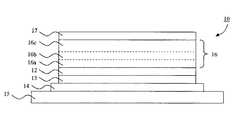
次に、図面を参照して、本発明の実施形態に係る有機発光素子について説明する。図1は、本発明の実施形態に係る有機発光素子の概略構成を示す縦断面図である。 Next, an organic light-emitting device according to an embodiment of the present invention will be described with reference to the drawings. FIG. 1 is a longitudinal sectional view showing a schematic configuration of an organic light emitting device according to an embodiment of the present invention.
図1に示すように、本発明の実施形態に係る有機発光素子10は、基板15上に陽極14が形成され、その上に有機化合物層として、ホール輸送層13、発光層12、電子注入輸送層16が形成され、さらにその上に陰極17が形成された構成となっている。 As shown in FIG. 1, an organic
以下、有機発光素子10を構成する各層の材料について具体的に説明する。 Hereinafter, the material of each layer which comprises the organic
基板15の材料としては、各種のガラス基板や、poly−SiでTFT等の駆動回路を形成したガラス基板、シリコンウエハー上に駆動回路を設けたもの等を挙げることができる。また、基板15と反対側から光を取り出す場合には、基板15は透明でなくてもよいが、基板15側から光を取り出す場合には、基板15は透明であることが好ましい。 Examples of the material of the
陽極14の材料としては、仕事関数の大きな導電性材料を選択することが好ましい。さらに、基板15と反対側から光を取り出す場合には、反射率の高い金属材料を選択することが好ましい。例えば、Cr、Pt、Ag、Au等の金属材料、及びこれらの金属材料を含む合金等が好適に用いられる。また、高反射率の金属材料上に、透明導電性材料の薄膜を形成したものを用いてもよい。また、透明導電性材料としてITO等のように仕事関数の大きな材料を用いる場合には、必ずしも仕事関数の大きな金属材料を選択する必要はない。 As a material for the
基板15と反対側から光を取り出す場合には、陰極17が透明であることが好ましく、陰極17の材料として、例えばITO等の透明導性電材料を用いることができる。また、金属材料を1nmから10nm程度の薄膜で形成し、透光性のある陰極17としてもよい。さらに、半透光性を有する陰極17を用いることにより、光の干渉効果を利用して、光の外部取り出し効率の向上を図るとともに、色純度の向上を図ることも可能である。 When extracting light from the side opposite to the
ホール輸送層13を形成する正孔輸送材料としては、トリフェニルジアミン誘導体、オキサジアゾール誘導体、ポリフィリン誘導体、スチルベン誘導体等の低分子化合物等を挙げることができるが、これらの材料に限定されるものではない。 Examples of the hole transport material forming the
発光層12の材料としては、単一の材料で所望の発光を得る材料、あるいはホスト材料にゲスト材料をドープしたものが用いられる。すなわち、ホスト材料及びゲスト材料を同時に真空蒸着し、それぞれの蒸着レートを調整することで、任意のドープ濃度とした発光層12を得ることができる。また、発光層12を形成する際に、適時、第二、第三のドーパント材料をドープしてもよい。 As the material of the
電子注入輸送層16を形成する電子輸送材料としては、アルミキノリノール誘導体、オキサジアゾール誘導体、トリアゾール誘導体、フェニルキノキサリン誘導体、シロール誘導体等を挙げることができるが、これらの材料に限定されるものではない。 Examples of the electron transport material for forming the electron injection /
電子注入輸送層16は、電子注入ドーパント材料のドープ濃度に応じて、発光層12側から順に、膜厚方向で3つの領域16a(第1領域)、16b(第2領域)、16c(第3領域)、が形成されている。各領域では、それぞれ所望の濃度で、電子輸送材料中に電子注入ドーパント材料であるアルカリ金属あるいはアルカリ金属化合物がドープされている。 The electron injecting and
ここで、領域16aのドープ濃度は、電子注入輸送層16の全体における平均ドープ濃度よりも小さく設定されている。具体的には、領域16aにおけるドープ濃度は、1.0重量%未満であることが好ましく、0.1重量%以下であることがさらに好ましく、0.01重量%以下であることがさらに一層好ましい。 Here, the doping concentration of the
また、領域16bのドープ濃度は、電子注入輸送層16の全体における平均ドープ濃度よりも大きく設定されている。具体的には、領域16bにおけるドープ濃度は、4重量%以上6重量%以下であることが好ましい。尚、領域16bの厚みは5nm以上20nm以下が好ましい。 Further, the doping concentration of the
また、領域16cのドープ濃度は、電子注入輸送層16の全体における平均ドープ濃度よりも小さく設定されている。具体的には、領域16cにおけるドープ濃度は、1.0重量%以下であることが好ましく、この範囲において0.1重量%以上であることがさらに好ましい。 Further, the doping concentration of the
このように、本実施形態の電子注入輸送層16は、膜厚方向の中央の領域16bが発光層側の領域16a及び陰極側の領域16cと比較してドープ濃度が大きくなるように、電子輸送材料に電子注入ドーパント材料がドープされている。すなわち、電子注入輸送層16を構成する膜厚方向の各領域16a,16b,16cでは、発光層12側から順に、ドープ濃度が小、大、小となっている。 Thus, the electron injecting and transporting
このように各領域の電子注入ドーパント材料の濃度を異ならせることによって、光取り出し効率の低下を招くことなく駆動耐久特性を向上させることができる。駆動耐久特性を向上させるためには16b(第2領域)の濃度を高くする必要があることが分かったが、16a(第1領域)、16c(第3領域)の濃度を同様に高くしても駆動耐久特性を向上させることはできなかった。一方、電子注入輸送層中の電子注入ドーパント材料の濃度を高くすると、発光層12で発光する光を外部に取り出す光取り出し効率が低下してしまうことが分かった。そのため、濃度を高くしても駆動耐久特性の向上との関係が見られない16a及び16cの濃度を低くすることが好ましい。したがって、本実施形態の有機発光素子の電子注入層は、16b(第2領域)の電子注入ドーパント材料の濃度を高めつつ、16a(第1領域)、16c(第3領域)の電子注入ドーパント材料の濃度を低くすることが好ましい。このようにすることによって、駆動耐久特性と、光取り出し効率の両方を満足する有機発光素子を得ることができる。 Thus, by varying the concentration of the electron injection dopant material in each region, it is possible to improve the driving durability characteristics without causing a decrease in light extraction efficiency. In order to improve the driving durability characteristics, it has been found that the concentration of 16b (second region) needs to be increased, but the concentration of 16a (first region) and 16c (third region) is similarly increased. However, the driving durability characteristics could not be improved. On the other hand, it was found that when the concentration of the electron injection dopant material in the electron injection transport layer is increased, the light extraction efficiency for extracting light emitted from the
さらに、本発明にかかる有機発光素子の電子注入層は、図2に示すように16cと電子注入ドーパント材料の濃度が異なる16d(第4領域)が、16cの陰極側に設けられていることが好ましい。16dの濃度を16cの濃度よりも高めることによって、陰極17から電子注入輸送層16への電子注入障壁を低減することができるため、駆動電圧を低減することができる。 Furthermore, as shown in FIG. 2, the electron injection layer of the organic light emitting device according to the present invention is provided with 16d (fourth region) having a different concentration of the electron injection dopant material on the cathode side of 16c. preferable. By increasing the concentration of 16d higher than the concentration of 16c, the electron injection barrier from the
領域16dのドープ濃度は、電子注入輸送層16の全体における平均ドープ濃度よりも大きく設定されている。具体的には、領域16dにおけるドープ濃度は、4重量%以上6.0重量%以下であることが好ましい。 The doping concentration of the region 16 d is set to be higher than the average doping concentration in the entire electron injecting and transporting
このように、図2に示す実施形態の電子注入輸送層16は、膜厚方向の中央の領域16bが発光層側の領域16a及び陰極側の領域16cと比較してドープ濃度が大きくなるように、電子輸送材料に電子注入ドーパント材料がドープされている。また、電子注入輸送層16を構成する陰極側領域16cのさらに陰極17側に陰極17に接する領域16dが存在し、この領域16dにおけるドープ濃度は、領域16cよりも大きくなっている。したがって、電子注入輸送層16を全体としてみると、膜厚方向の各領域16a,16b,16c,16dでは、発光層12側から順にドープ濃度が小、大、小、大となっている。 As described above, the electron injecting and transporting
各領域における電子注入ドーパント材料のドープ濃度を上述した数値範囲とすることにより、光取り出し効率の低下を招くことなく駆動耐久特性を向上させることができるとともに、駆動電圧を低減することができる。 By setting the doping concentration of the electron-injecting dopant material in each region within the above-described numerical range, it is possible to improve driving durability characteristics and reduce driving voltage without causing a decrease in light extraction efficiency.
以上、本発明にかかる有機発光素子の構成について説明したが、電子注入輸送層の各領域の電子注入ドーパント材料の濃度は、膜厚方向で一定の濃度になっていなくてもよい。つまり、隣接する領域の境界付近の電子注入ドーパント材料の濃度は、それぞれの領域の電子注入ドーパント材料の濃度の間の濃度となっており、濃度勾配を持っていてもよい。 Although the configuration of the organic light emitting device according to the present invention has been described above, the concentration of the electron injection dopant material in each region of the electron injection transport layer may not be a constant concentration in the film thickness direction. That is, the concentration of the electron injection dopant material in the vicinity of the boundary between adjacent regions is a concentration between the concentration of the electron injection dopant material in each region, and may have a concentration gradient.
ここで、本発明で用いている、電子注入輸送層の効果について説明する。特許文献3で開示されている様に、アルカリ金属、或いはアルカリ金属化合物と電子輸送材料を共蒸着した層は、電極からの電子注入性を改善させることができると共に、その抵抗値も非常に低いことが知られている。この効果はアルカリ金属及びアルカリ金属化合物と電子輸送材料との相互作用による。 Here, the effect of the electron injecting and transporting layer used in the present invention will be described. As disclosed in Patent Document 3, a layer obtained by co-evaporation of an alkali metal or an alkali metal compound and an electron transport material can improve the electron injectability from the electrode and has a very low resistance value. It is known. This effect is due to the interaction between the alkali metal and the alkali metal compound and the electron transport material.
ITO等のように仕事関数の高い電極から電子を注入する場合には出来るだけドープ濃度が高い方が駆動電圧を低減できる。一方、電子注入層内の輸送特性は濃度依存が少なく、比較的低濃度でも良好な輸送特性を得ることが出来る。 In the case where electrons are injected from an electrode having a high work function such as ITO, the driving voltage can be reduced when the doping concentration is as high as possible. On the other hand, the transport properties in the electron injection layer are less dependent on concentration, and good transport properties can be obtained even at relatively low concentrations.
一方このような電子注入輸送層は、その相互作用に起因して、光学吸収が増加し、その量はドープ濃度と共に増加するという性質がある。よって発光取り出し効率を向上させるには、出来るだけ高濃度のドープ領域を少なくした方が良い。 On the other hand, such an electron injecting and transporting layer has the property that the optical absorption increases due to the interaction, and the amount thereof increases with the doping concentration. Therefore, in order to improve the light emission extraction efficiency, it is better to reduce the concentration region as high as possible.
また本発明で得られる、耐久特性が向上する効果については、詳細には明らかになっていないが、電子輸送材料にアルカリ金属或いはアルカリ金属化合物をドープすることにより、発光層と電子注入輸送層との物理的接合が変化することによると推定される。電子注入輸送層におけるこれらのドープ濃度を発光層側より小大とすることにより、発光層への電子注入、或いは発光層、電子注入輸送層界面における正孔の振る舞いが変化し耐久特性が向上したもと考えられる。 In addition, the effect of improving durability characteristics obtained in the present invention is not clarified in detail, but by doping an electron transport material with an alkali metal or an alkali metal compound, a light emitting layer, an electron injection transport layer, It is presumed that the physical junction of the material changes. By making these doping concentrations in the electron injecting and transporting layer smaller than those on the light emitting layer side, the electron injection into the light emitting layer or the behavior of holes at the interface between the light emitting layer and the electron injecting and transporting layer was changed, and the durability characteristics were improved. Originally considered.
これらの効果はアルカリ金属或いはアルカリ金属化合物と電子輸送材料の相互作用により発現するものであり、セシウム化合物だけでなく、ルビジウム、カリウム、ナトリウム、リチウム及びその化合物でもその効果が期待できる。特にセシウム化合物ではその電子供与性の高さより最も効果が大きい。 These effects are manifested by the interaction between the alkali metal or alkali metal compound and the electron transport material, and the effect can be expected not only with the cesium compound but also with rubidium, potassium, sodium, lithium, and compounds thereof. In particular, the cesium compound is most effective than its electron donating property.
本実施形態で用いる陰極、陽極及び有機化合物層の形成方法は、特に限定されるものではない。例えば、有機材料の場合には、電解重合法、キャスティング法、スピンコート法、浸漬コート法、スクリーン印刷法、マイクロモールド法、マイクロコンタクトプリンティング法、ロール塗布法、インクジェット法、LB法等を用いることができる。また、用いる材料に応じて、真空蒸着法、CVD法、電子ビーム蒸着法、抵抗加熱蒸着法、スパッタ法等も、陰極、陽極及び有機化合物層の有効な形成方法となる。また、陰極、陽極及び有機化合物層は、フォトリソグラフおよびエッチング処理により所望の形状にパターニングすることができる。その他、ソフトリソグラフ、インクジェット法も有効なパターニング方法である。 The formation method of the cathode, anode, and organic compound layer used in the present embodiment is not particularly limited. For example, in the case of an organic material, an electrolytic polymerization method, a casting method, a spin coating method, a dip coating method, a screen printing method, a micro mold method, a micro contact printing method, a roll coating method, an ink jet method, an LB method, or the like is used. Can do. Depending on the material used, a vacuum deposition method, a CVD method, an electron beam deposition method, a resistance heating deposition method, a sputtering method, and the like are also effective methods for forming the cathode, the anode, and the organic compound layer. Further, the cathode, the anode and the organic compound layer can be patterned into a desired shape by photolithography and etching treatment. In addition, soft lithography and ink jet methods are also effective patterning methods.
本実施形態で用いる陰極、陽極及び有機化合物層の膜厚は特に限定はされないが、0.1nm乃至10μmの範囲が好ましい。 The thickness of the cathode, anode and organic compound layer used in the present embodiment is not particularly limited, but is preferably in the range of 0.1 nm to 10 μm.
また、本実施形態において得られる有機発光素子を面内に複数配置して、ディスプレイ等の情報表示部に用いることができる。ディスプレイのサイズは特に制限されないが、例えば、1インチから30インチまでの大きさであることが好ましい。画素数も特に制限はない。例えばQVGA(320×240画素)、VGA(640×480画素)、XGA(1024×768画素)、SXGA(1280×1024画素)、UXGA(1600×1200画素)、QXGA(2048×1536画素)とすることができる。また、ディスプレイは、カラー表示できることが好ましい。この場合、赤、青、緑の発光素子を独立に配列させることで表示する方法、またはカラーフィルターを用いる方法のいずれを用いてもよい。また、ディスプレイの駆動方式としては、単純マトリックス方式、またはアクティブマトリックス方式を用いることができる。 In addition, a plurality of organic light emitting elements obtained in the present embodiment can be arranged in the plane and used for an information display unit such as a display. The size of the display is not particularly limited, but is preferably 1 inch to 30 inches, for example. The number of pixels is not particularly limited. For example, QVGA (320 × 240 pixels), VGA (640 × 480 pixels), XGA (1024 × 768 pixels), SXGA (1280 × 1024 pixels), UXGA (1600 × 1200 pixels), and QXGA (2048 × 1536 pixels). be able to. The display is preferably capable of color display. In this case, any of a method of displaying by arranging red, blue, and green light emitting elements independently or a method of using a color filter may be used. As a display driving method, a simple matrix method or an active matrix method can be used.
また、有機発光素子を空気中の水分、酸素等から遮断するために、有機発光素子上にキャップを設けることが好ましい。この際、基板の膜面側から光を取り出す場合には、キャップの材料として透光性を有する部材を用いることが好ましく、例えばガラス等が用いられる。また、キャップと有機発光素子との間に空隙を設け、乾燥剤等を配置してもよい。 Moreover, it is preferable to provide a cap on the organic light emitting element in order to shield the organic light emitting element from moisture, oxygen, etc. in the air. At this time, when light is extracted from the film surface side of the substrate, it is preferable to use a light-transmitting member as the material of the cap, for example, glass or the like. Moreover, a space | gap may be provided between a cap and an organic light emitting element, and a desiccant etc. may be arrange | positioned.
また、SiN、SiO等の無機材料や、高分子材料等の膜を有機発光素子上に配置して外気と遮断してもよい。 Alternatively, an inorganic material such as SiN or SiO, or a film made of a polymer material or the like may be disposed on the organic light emitting element to block the outside air.
以下、具体的な実施例を用いて、本発明の有機発光素子についてさらに詳細に説明する。なお、本発明の有機発光素子は、以下の実施例に限定されるものではない。 Hereinafter, the organic light-emitting device of the present invention will be described in more detail using specific examples. The organic light emitting device of the present invention is not limited to the following examples.
<実施例1及び実施例2、比較例1乃至比較例4>
上述したように、本発明に係る有機発光素子10は、基板15上に陽極14が形成され、その上に有機化合物層として、ホール輸送層13、発光層12、電子注入輸送層16が形成され、さらにその上に陰極17が形成されている(図1参照)。ここで、本発明の実施例に係る有機発光素子10を構成する各層は、以下に示す具体的な材料を用いている。<Example 1 and Example 2, Comparative Example 1 to Comparative Example 4>
As described above, in the organic
すなわち、基板15としてガラスを用い、陽極14としてAgとITOの積層膜を用いる。また、ホール輸送層13としてHT−1を用い、発光層12としてEM−1とEM−2の共蒸着層を用い、電子注入輸送層としてET−1と炭酸セシウムの共蒸着層を用いる。さらに、陰極としてITO膜を用いる。 That is, glass is used as the
以下に、実施例1及び実施例2、比較例1乃至比較例4の有機発光素子の製造手順を説明する。 Below, the manufacturing procedure of the organic light emitting element of Example 1, Example 2, and Comparative Examples 1 to 4 will be described.
ガラス基板(コーニング社:1737)上に銀を100nm、ITO膜を20nm成膜して透明基板(基板15)を形成し、さらにフォトリソグラフィー法によりパターニングして、透明電極(陽極14)を形成する。 A transparent substrate (substrate 15) is formed on a glass substrate (Corning Inc .: 1737) by forming silver with a thickness of 100 nm and an ITO film with a thickness of 20 nm, and then patterning by photolithography to form a transparent electrode (anode 14). .
この透明電極(陽極14)を、大気圧下でUV−O3洗浄した後、以下の有機化合物層を10-4Paの真空チャンバー内で抵抗加熱による真空蒸着法を用いて連続成膜する。その後、スパッタ法を用いてITO膜を成膜し、実施例1及び実施例2、比較例1乃至比較例4の有機発光素子10を得た。After this transparent electrode (anode 14) is UV-O3 washed under atmospheric pressure, the following organic compound layers are continuously formed in a vacuum chamber of 10−4 Pa using a vacuum evaporation method using resistance heating. Thereafter, an ITO film was formed by sputtering, and organic
ここで、各膜厚等は以下の通りである。 Here, each film thickness etc. are as follows.
ホール輸送層13は、HT−1(20nm)となっている。また、発光層12は、EM−1及びEM−2の共蒸着層(比率EM−1:EM−2=87:13)(20nm)となっている。電子注入輸送層16は、ET−1及び炭酸セシウムの共蒸着層(50nm)となっている。 The
また、実施例1及び実施例2、比較例1乃至比較例4で用いている材料の化学式は、以下の通りである。 The chemical formulas of the materials used in Examples 1 and 2 and Comparative Examples 1 to 4 are as follows.

ここで、ET−1における炭酸セシウムのドープ濃度は、蒸着工程における蒸着スピードをその濃度に対応するように制御し、所望の濃度に設定した。使用した材料及びその膜厚、作成した素子の特性は、以下の表1に示す通りである。 Here, the doping concentration of cesium carbonate in ET-1 was set to a desired concentration by controlling the vapor deposition speed in the vapor deposition step so as to correspond to the concentration. The materials used, their film thicknesses, and the characteristics of the fabricated devices are as shown in Table 1 below.
<実施例1>
電子注入輸送層における炭酸セシウムの濃度を領域aで0.01%、領域bで5.10%、領域cで0.5%、領域dで4.9%として実施例1の有機発光素子を作成した。なお、領域a,領域b,領域c,領域dは、図1における領域16a,16b,16c,16dにそれぞれ対応する(以下の各実施例および各比較例において同様)。<Example 1>
In the electron injecting and transporting layer, the concentration of cesium carbonate in the region a is 0.01%, the region b is 5.10%, the region c is 0.5%, and the region d is 4.9%. Created. Note that the region a, the region b, the region c, and the region d correspond to the
実施例1の有機発光素子を20mA/cm2の電流密度で駆動したところ、輝度463cd/m2、駆動電圧3.1Vであった。また、実施例1の有機発光素子を20mA/cm2で連続駆動したところ、90%の輝度まで劣化する時間が約127hrであった。同条件で作成した実施例1と同様の有機発光素子を約200日間常温下で保存した後、20mA/cm2の電流を印加した際の駆動電圧は3.3Vであった。When the organic light emitting device of Example 1 was driven at a current density of 20 mA / cm2 , the luminance was 463 cd / m2 and the driving voltage was 3.1 V. Further, when the organic light-emitting device of Example 1 was continuously driven at 20 mA / cm2 , the time for degradation to 90% luminance was about 127 hr. The organic light emitting device similar to that of Example 1 created under the same conditions was stored at room temperature for about 200 days, and then the driving voltage when a current of 20 mA / cm2 was applied was 3.3V.
<比較例1>
電子注入輸送層における炭酸セシウムの濃度を領域aで0.01%、領域bで4.9%、領域cで4.9%、領域dで4.9%として比較例1の有機発光素子を作成した。<Comparative Example 1>
In the electron injecting and transporting layer, the concentration of cesium carbonate was 0.01% in the region a, 4.9% in the region b, 4.9% in the region c, and 4.9% in the region d. Created.
比較例1の有機発光素子を20mA/cm2の電流密度で駆動したところ、輝度402cd/m2、駆動電圧3.1Vであり、実施例1と比較して輝度が低下した。また、比較例1の有機発光素子を20mA/cm2で連続駆動したところ、90%の輝度まで劣化する時間が約135hrであり、実施例1と大きな違いはなかった。同条件で作成した比較例1と同様の有機発光素子を約200日間常温下で保存した後、20mA/cm2の電流を印加した際の駆動電圧は3.1Vであった。When the organic light emitting device of Comparative Example 1 was driven at a current density of 20 mA / cm2 , the luminance was 402 cd / m2 and the driving voltage was 3.1 V, and the luminance was lower than that of Example 1. Further, when the organic light emitting device of Comparative Example 1 was continuously driven at 20 mA / cm2 , the degradation time to 90% was about 135 hr, which was not significantly different from Example 1. The organic light emitting device similar to Comparative Example 1 prepared under the same conditions was stored at room temperature for about 200 days, and then the driving voltage when a current of 20 mA / cm2 was applied was 3.1V.
<比較例2>
電子注入輸送層における炭酸セシウムの濃度を領域aで0.005%、領域bで0.5%、領域cで0.5%、領域dで0.5%として比較例2の有機発光素子を作成した。<Comparative example 2>
In the electron injecting and transporting layer, the concentration of cesium carbonate is 0.005% in the region a, 0.5% in the region b, 0.5% in the region c, and 0.5% in the region d. Created.
比較例2の有機発光素子を20mA/cm2の電流密度で駆動したところ、輝度514cd/m2、駆動電圧3.5Vであり、実施例1と比較して輝度は向上したものの、駆動電圧が上昇した。また、比較例2の有機発光素子を20mA/cm2で連続駆動したところ、90%の輝度まで劣化する時間が約20hrであり駆動劣化特性が著しく劣った。同条件で作成した比較例2と同様の有機発光素子を約200日間常温下で保存した後、20mA/cm2の電流を印加した際の駆動電圧は3.5Vであった。When the organic light emitting device of Comparative Example 2 was driven at a current density of 20 mA / cm2 , the luminance was 514 cd / m2 and the driving voltage was 3.5 V. Although the luminance was improved as compared with Example 1, the driving voltage was Rose. Further, when the organic light emitting device of Comparative Example 2 was continuously driven at 20 mA / cm2 , the deterioration time to 90% was about 20 hours, and the drive deterioration characteristics were extremely inferior. The organic light emitting device similar to Comparative Example 2 prepared under the same conditions was stored at room temperature for about 200 days, and then the driving voltage when a current of 20 mA / cm2 was applied was 3.5V.
<実施例2>
電子注入輸送層における炭酸セシウムの濃度を領域aで0.01%、領域bで4.8%、領域cで0.5%、領域dで0.5%として実施例2の有機発光素子を作成した。<Example 2>
In the electron injecting and transporting layer, the concentration of cesium carbonate in the region a is 0.01%, the region b is 4.8%, the region c is 0.5%, and the region d is 0.5%. Created.
実施例2の有機発光素子を20mA/cm2の電流密度で駆動したところ、輝度470cd/m2、駆動電圧3.5Vであった。また実施例2の有機発光素子2を20mA/cm2で連続駆動したところ、90%の輝度まで劣化する時間が約119hrであった。すなわち、実施例2では、比較例1と比較して駆動電圧は上昇したものの、輝度が向上し、耐久特性は比較例1とほぼ同レベルにあった。同条件で作成した実施例2と同様の有機発光素子を約200日間常温下で保存した後、20mA/cm2の電流を印加した際の駆動電圧は3.5Vであった。When the organic light emitting device of Example 2 was driven at a current density of 20 mA / cm2 , the luminance was 470 cd / m2 and the driving voltage was 3.5V. Further, when the organic light emitting device 2 of Example 2 was continuously driven at 20 mA / cm2, it took about 119 hours to deteriorate to 90% luminance. That is, in Example 2, although the drive voltage was increased as compared with Comparative Example 1, the luminance was improved and the durability characteristics were almost at the same level as Comparative Example 1. The organic light-emitting device similar to that of Example 2 created under the same conditions was stored at room temperature for about 200 days, and then the driving voltage when a current of 20 mA / cm2 was applied was 3.5V.
<比較例3>
電子注入輸送層における炭酸セシウムの濃度を領域aで0.005%、領域bで0.5%、領域cで0.5%、領域dで5.1%として比較例3の有機発光素子を作成した。<Comparative Example 3>
In the electron injecting and transporting layer, the concentration of cesium carbonate was 0.005% in the region a, 0.5% in the region b, 0.5% in the region c, and 5.1% in the region d. Created.
比較例3の有機発光素子を20mA/cm2の電流密度で駆動したところ、輝度471cd/m2、駆動電圧3.1Vであった。また、比較例3の有機発光素子を20mA/cm2で連続駆動したところ、90%の輝度まで劣化する時間が約25hrであった。すなわち、比較例3では、実施例1と比較して輝度は向上したものの、駆動劣化特性は著しく劣る結果となった。同条件で作成した比較例3と同様の有機発光素子を約200日間常温下で保存した後、20mA/cm2の電流を印加した際の駆動電圧は3.3Vであった。When the organic light emitting device of Comparative Example 3 was driven at a current density of 20 mA / cm2 , the luminance was 471 cd / m2 and the driving voltage was 3.1V. Further, when the organic light-emitting device of Comparative Example 3 was continuously driven at 20 mA / cm2 , the degradation time to 90% was about 25 hr. That is, in Comparative Example 3, although the luminance was improved as compared with Example 1, the driving deterioration characteristic was remarkably inferior. The organic light emitting device similar to Comparative Example 3 prepared under the same conditions was stored at room temperature for about 200 days, and then the driving voltage when a current of 20 mA / cm2 was applied was 3.3V.
<比較例4>
電子注入輸送層における炭酸セシウムの濃度を領域aで0.005%、領域bで5.1%、領域cで0%、領域dで4.8%として比較例4の有機発光素子を作成した。<Comparative example 4>
The organic light emitting device of Comparative Example 4 was prepared by setting the concentration of cesium carbonate in the electron injecting and transporting layer to 0.005% in the region a, 5.1% in the region b, 0% in the region c, and 4.8% in the region d. .
比較例4の有機発光素子を20mA/cm2の電流密度で駆動したところ、輝度459cd/m2、駆動電圧4.2Vであった。また、比較例4の有機発光素子を20mA/cm2で連続駆動したところ、90%の輝度まで劣化する時間が約50hrであった。比較例4では、実施例1及び実施例2と比較して、輝度が若干劣るとともに、駆動電圧及び駆動劣化特性が著しく劣る結果となった。同条件で作成した比較例4と同様の有機発光素子を約200日間常温下で保存した後、20mA/cm2の電流を印加した際の駆動電圧は4.5Vであった。When the organic light emitting device of Comparative Example 4 was driven at a current density of 20 mA / cm2 , the luminance was 459 cd / m2 and the driving voltage was 4.2V. Further, when the organic light-emitting device of Comparative Example 4 was continuously driven at 20 mA / cm2 , the time for degradation to 90% luminance was about 50 hr. In Comparative Example 4, as compared with Example 1 and Example 2, the luminance was slightly inferior, and the driving voltage and the driving deterioration characteristic were remarkably inferior. The organic light-emitting device similar to Comparative Example 4 prepared under the same conditions was stored at room temperature for about 200 days, and then the drive voltage when a current of 20 mA / cm2 was applied was 4.5V.
<実施例3>
実施例3の有機発光素子は、電子注入輸送層としてET−2と炭酸セシウムの共蒸着層を用いる以外は、実施例1と同様の手順で作成したものである。<Example 3>
The organic light-emitting device of Example 3 was prepared in the same procedure as in Example 1 except that a co-deposited layer of ET-2 and cesium carbonate was used as the electron injecting and transporting layer.
実施例3の有機発光素子を20mA/cm2の電流密度で駆動したところ、輝度431cd/m2、駆動電圧3.2Vであった。また、実施例3の素子を20mA/cm2で連続駆動したところ、90%の輝度まで劣化する時間が約121hrであった。実施例3では、実施例1及び実施例2とほぼ同程度の駆動電圧及び駆動劣化特性とすることができた。同条件で作成した実施例3と同様の有機発光素子を約200日間常温下で保存した後、20mA/cm2の電流を印加した際の駆動電圧は3.2Vであった。When the organic light emitting device of Example 3 was driven at a current density of 20 mA / cm2 , the luminance was 431 cd / m2 and the driving voltage was 3.2 V. Further, when the element of Example 3 was continuously driven at 20 mA / cm2, it took about 121 hours to deteriorate to a luminance of 90%. In Example 3, the driving voltage and driving deterioration characteristics were almost the same as those in Example 1 and Example 2. An organic light emitting device similar to that of Example 3 created under the same conditions was stored at room temperature for about 200 days, and then a driving voltage when a current of 20 mA / cm2 was applied was 3.2V.
<実施例と比較例の比較結果>
本発明によれば、電子注入輸送層において、膜厚方向で、ドープ濃度が発光層側から順に小、大、小、大となる様に設定することにより、光取り出し効率の低下を招くことなく駆動電圧を低減することができると共に、駆動耐久特性を向上させることができる。<Comparison result of Example and Comparative Example>
According to the present invention, in the electron injecting and transporting layer, by setting the dope concentration in the film thickness direction from the light emitting layer side in the order of decreasing, increasing, decreasing, and increasing, the light extraction efficiency does not decrease. The driving voltage can be reduced and driving durability characteristics can be improved.
10 有機発光素子
12 発光層
13 ホール輸送層
14 陽極
15 基板
16 電子注入輸送層
17 陰極DESCRIPTION OF
Claims (6)
Translated fromJapanese前記電子注入輸送層は、電子輸送材料と、電子注入ドーパント材料としてアルカリ金属あるいはアルカリ金属化合物、を含む有機発光素子において、
前記電子注入輸送層は、前記発光層側から順に、前記電子注入ドーパント材料の濃度の異なる第1領域、第2領域、第3領域、を有しており、
前記第2領域の前記電子注入ドーパント材料の濃度は、前記第1領域および前記第3領域の前記電子注入ドーパント材料の濃度よりも高いことを特徴とする有機発光素子。An anode and a cathode disposed opposite to each other, a light emitting layer formed between the anode and the cathode, and formed between the cathode and the light emitting layer. An electron injecting and transporting layer in contact,
The electron injecting and transporting layer includes an electron transporting material and an alkali metal or an alkali metal compound as an electron injecting dopant material.
The electron injecting and transporting layer has, in order from the light emitting layer side, a first region, a second region, and a third region having different concentrations of the electron injecting dopant material,
The organic light emitting device, wherein the concentration of the electron injection dopant material in the second region is higher than the concentration of the electron injection dopant material in the first region and the third region.
前記第4領域の前記電子注入ドーパント材料の濃度は、前記第3領域の前記電子注入ドーパント材料の濃度よりも高いことを特徴とする請求項1または請求項2のいずれか1項に記載の有機発光素子。The electron injection layer has a fourth region between the third region and the cathode,
3. The organic material according to claim 1, wherein a concentration of the electron injection dopant material in the fourth region is higher than a concentration of the electron injection dopant material in the third region. Light emitting element.
Priority Applications (2)
| Application Number | Priority Date | Filing Date | Title |
|---|---|---|---|
| JP2007068479AJP2007294901A (en) | 2006-03-31 | 2007-03-16 | Organic light emitting device |
| US11/692,545US7605532B2 (en) | 2006-03-31 | 2007-03-28 | Organic light emitting device |
Applications Claiming Priority (2)
| Application Number | Priority Date | Filing Date | Title |
|---|---|---|---|
| JP2006097181 | 2006-03-31 | ||
| JP2007068479AJP2007294901A (en) | 2006-03-31 | 2007-03-16 | Organic light emitting device |
Publications (2)
| Publication Number | Publication Date |
|---|---|
| JP2007294901Atrue JP2007294901A (en) | 2007-11-08 |
| JP2007294901A5 JP2007294901A5 (en) | 2010-04-15 |
Family
ID=38557823
Family Applications (1)
| Application Number | Title | Priority Date | Filing Date |
|---|---|---|---|
| JP2007068479APendingJP2007294901A (en) | 2006-03-31 | 2007-03-16 | Organic light emitting device |
Country Status (2)
| Country | Link |
|---|---|
| US (1) | US7605532B2 (en) |
| JP (1) | JP2007294901A (en) |
Cited By (4)
| Publication number | Priority date | Publication date | Assignee | Title |
|---|---|---|---|---|
| KR101223615B1 (en) | 2010-12-31 | 2013-01-17 | 서울대학교 산학협력단 | Inverted organic light-emitting diode and flat display device comprising the same |
| JP2013539182A (en)* | 2010-09-06 | 2013-10-17 | エルジー・ケム・リミテッド | Organic electronic device substrate and organic electronic device including the same |
| JP2015053493A (en)* | 2008-10-01 | 2015-03-19 | エルジー・ケム・リミテッド | Organic light emitting element and method of manufacturing the same |
| JP2016115717A (en)* | 2014-12-11 | 2016-06-23 | 株式会社Joled | Organic el element and method of manufacturing organic el element |
Families Citing this family (5)
| Publication number | Priority date | Publication date | Assignee | Title |
|---|---|---|---|---|
| JP4898560B2 (en)* | 2006-06-23 | 2012-03-14 | キヤノン株式会社 | Organic light emitting device |
| TWI500196B (en)* | 2007-04-30 | 2015-09-11 | Lg Chemical Ltd | Organic light emitting device and method of producing the same |
| KR101045264B1 (en)* | 2008-09-09 | 2011-06-29 | 네오뷰코오롱 주식회사 | Display device, mobile device having same and display control method |
| KR102470303B1 (en)* | 2015-10-27 | 2022-11-28 | 삼성디스플레이 주식회사 | Organic electroluminescent device and display device including the same |
| US20230023178A1 (en)* | 2021-07-22 | 2023-01-26 | Wuhan China Star Optoelectronics Semiconductor Display Technology Co., Ltd. | Display panel and mobile terminal |
Citations (2)
| Publication number | Priority date | Publication date | Assignee | Title |
|---|---|---|---|---|
| JP2003234196A (en)* | 2002-01-31 | 2003-08-22 | Eastman Kodak Co | Organic electroluminescent device |
| JP2003272868A (en)* | 2002-03-20 | 2003-09-26 | Denso Corp | Organic EL device |
Family Cites Families (7)
| Publication number | Priority date | Publication date | Assignee | Title |
|---|---|---|---|---|
| JP4486713B2 (en) | 1997-01-27 | 2010-06-23 | 淳二 城戸 | Organic electroluminescent device |
| JPH10270171A (en) | 1997-01-27 | 1998-10-09 | Junji Kido | Organic electroluminescent device |
| JP4076769B2 (en) | 2000-12-28 | 2008-04-16 | 株式会社半導体エネルギー研究所 | Light emitting device and electric appliance |
| SG2009086778A (en) | 2000-12-28 | 2016-11-29 | Semiconductor Energy Lab Co Ltd | Luminescent device |
| CN101916829B (en) | 2001-06-15 | 2012-05-09 | 佳能株式会社 | organic electroluminescent element |
| JP2005063910A (en) | 2003-08-20 | 2005-03-10 | Canon Inc | ORGANIC LIGHT EMITTING DEVICE AND MANUFACTURING METHOD THEREOF |
| US20060289882A1 (en)* | 2004-07-30 | 2006-12-28 | Kazuki Nishimura | Organic electroluminescent element and organic electroluminescent display device |
- 2007
- 2007-03-16JPJP2007068479Apatent/JP2007294901A/enactivePending
- 2007-03-28USUS11/692,545patent/US7605532B2/ennot_activeExpired - Fee Related
Patent Citations (2)
| Publication number | Priority date | Publication date | Assignee | Title |
|---|---|---|---|---|
| JP2003234196A (en)* | 2002-01-31 | 2003-08-22 | Eastman Kodak Co | Organic electroluminescent device |
| JP2003272868A (en)* | 2002-03-20 | 2003-09-26 | Denso Corp | Organic EL device |
Cited By (6)
| Publication number | Priority date | Publication date | Assignee | Title |
|---|---|---|---|---|
| JP2015053493A (en)* | 2008-10-01 | 2015-03-19 | エルジー・ケム・リミテッド | Organic light emitting element and method of manufacturing the same |
| US9587172B2 (en) | 2008-10-01 | 2017-03-07 | Lg Display Co., Ltd. | Organic light-emitting diode and method of manufacturing the same |
| JP2013539182A (en)* | 2010-09-06 | 2013-10-17 | エルジー・ケム・リミテッド | Organic electronic device substrate and organic electronic device including the same |
| US9257675B2 (en) | 2010-09-06 | 2016-02-09 | Lg Chem, Ltd. | Substrate for an organic electronic device and an organic electronic device comprising the same |
| KR101223615B1 (en) | 2010-12-31 | 2013-01-17 | 서울대학교 산학협력단 | Inverted organic light-emitting diode and flat display device comprising the same |
| JP2016115717A (en)* | 2014-12-11 | 2016-06-23 | 株式会社Joled | Organic el element and method of manufacturing organic el element |
Also Published As
| Publication number | Publication date |
|---|---|
| US20070228948A1 (en) | 2007-10-04 |
| US7605532B2 (en) | 2009-10-20 |
Similar Documents
| Publication | Publication Date | Title |
|---|---|---|
| JP2007294901A (en) | Organic light emitting device | |
| KR100932940B1 (en) | Organic light emitting display device | |
| US9530962B2 (en) | Patterning method for OLEDs | |
| JP4898560B2 (en) | Organic light emitting device | |
| JP4411288B2 (en) | Display device | |
| JP2007234241A (en) | Organic el element | |
| KR100844788B1 (en) | Fabrication method for organic light emitting device and organic light emitting device fabricated by the same method | |
| KR102000292B1 (en) | Organic light emitting display device and method for manufacturing thereof | |
| WO2007111153A1 (en) | Organic light emitting device array | |
| JP2011061016A (en) | Organic electroluminescent element | |
| JP2010055926A (en) | Organic electroluminescent element and its manufacturing method | |
| JP2010062067A (en) | Method of manufacturing display device, and display device | |
| JP4770699B2 (en) | Display element | |
| JP2003068470A (en) | Display element | |
| JP2008141174A (en) | Organic light emitting device | |
| US8466455B2 (en) | Device structure | |
| TWI569492B (en) | Organic light-emitting element | |
| JP2009070621A (en) | Display device | |
| JP2010010576A (en) | Organic light emitting element array | |
| JP4857498B2 (en) | Display element | |
| KR101738377B1 (en) | Organic light emitting display device and method for manufacturing thereof | |
| JP2007036127A (en) | Organic electroluminescent element | |
| KR20080011623A (en) | Electroluminescent element and manufacturing method thereof | |
| KR100705311B1 (en) | Organic electroluminescent device and manufacturing method thereof | |
| JP4824776B2 (en) | Organic light emitting device manufacturing method and organic light emitting device manufactured thereby |
Legal Events
| Date | Code | Title | Description |
|---|---|---|---|
| A521 | Request for written amendment filed | Free format text:JAPANESE INTERMEDIATE CODE: A523 Effective date:20100226 | |
| A621 | Written request for application examination | Free format text:JAPANESE INTERMEDIATE CODE: A621 Effective date:20100226 | |
| A977 | Report on retrieval | Free format text:JAPANESE INTERMEDIATE CODE: A971007 Effective date:20110914 | |
| A131 | Notification of reasons for refusal | Free format text:JAPANESE INTERMEDIATE CODE: A131 Effective date:20110920 | |
| A02 | Decision of refusal | Free format text:JAPANESE INTERMEDIATE CODE: A02 Effective date:20120306 |