JP2007287922A - Multilayer semiconductor device and manufacturing method thereof - Google Patents
Multilayer semiconductor device and manufacturing method thereofDownload PDFInfo
- Publication number
- JP2007287922A JP2007287922AJP2006113529AJP2006113529AJP2007287922AJP 2007287922 AJP2007287922 AJP 2007287922AJP 2006113529 AJP2006113529 AJP 2006113529AJP 2006113529 AJP2006113529 AJP 2006113529AJP 2007287922 AJP2007287922 AJP 2007287922A
- Authority
- JP
- Japan
- Prior art keywords
- wiring
- semiconductor device
- semiconductor chip
- sealing body
- product forming
- Prior art date
- Legal status (The legal status is an assumption and is not a legal conclusion. Google has not performed a legal analysis and makes no representation as to the accuracy of the status listed.)
- Granted
Links
Images


Classifications
- H—ELECTRICITY
- H01—ELECTRIC ELEMENTS
- H01L—SEMICONDUCTOR DEVICES NOT COVERED BY CLASS H10
- H01L24/00—Arrangements for connecting or disconnecting semiconductor or solid-state bodies; Methods or apparatus related thereto
- H01L24/93—Batch processes
- H01L24/95—Batch processes at chip-level, i.e. with connecting carried out on a plurality of singulated devices, i.e. on diced chips
- H01L24/97—Batch processes at chip-level, i.e. with connecting carried out on a plurality of singulated devices, i.e. on diced chips the devices being connected to a common substrate, e.g. interposer, said common substrate being separable into individual assemblies after connecting
- H—ELECTRICITY
- H01—ELECTRIC ELEMENTS
- H01L—SEMICONDUCTOR DEVICES NOT COVERED BY CLASS H10
- H01L25/00—Assemblies consisting of a plurality of semiconductor or other solid state devices
- H01L25/03—Assemblies consisting of a plurality of semiconductor or other solid state devices all the devices being of a type provided for in a single subclass of subclasses H10B, H10D, H10F, H10H, H10K or H10N, e.g. assemblies of rectifier diodes
- H01L25/04—Assemblies consisting of a plurality of semiconductor or other solid state devices all the devices being of a type provided for in a single subclass of subclasses H10B, H10D, H10F, H10H, H10K or H10N, e.g. assemblies of rectifier diodes the devices not having separate containers
- H01L25/065—Assemblies consisting of a plurality of semiconductor or other solid state devices all the devices being of a type provided for in a single subclass of subclasses H10B, H10D, H10F, H10H, H10K or H10N, e.g. assemblies of rectifier diodes the devices not having separate containers the devices being of a type provided for in group H10D89/00
- H01L25/0657—Stacked arrangements of devices
- H—ELECTRICITY
- H01—ELECTRIC ELEMENTS
- H01L—SEMICONDUCTOR DEVICES NOT COVERED BY CLASS H10
- H01L25/00—Assemblies consisting of a plurality of semiconductor or other solid state devices
- H01L25/03—Assemblies consisting of a plurality of semiconductor or other solid state devices all the devices being of a type provided for in a single subclass of subclasses H10B, H10D, H10F, H10H, H10K or H10N, e.g. assemblies of rectifier diodes
- H01L25/10—Assemblies consisting of a plurality of semiconductor or other solid state devices all the devices being of a type provided for in a single subclass of subclasses H10B, H10D, H10F, H10H, H10K or H10N, e.g. assemblies of rectifier diodes the devices having separate containers
- H01L25/105—Assemblies consisting of a plurality of semiconductor or other solid state devices all the devices being of a type provided for in a single subclass of subclasses H10B, H10D, H10F, H10H, H10K or H10N, e.g. assemblies of rectifier diodes the devices having separate containers the devices being integrated devices of class H10
- H—ELECTRICITY
- H01—ELECTRIC ELEMENTS
- H01L—SEMICONDUCTOR DEVICES NOT COVERED BY CLASS H10
- H01L2224/00—Indexing scheme for arrangements for connecting or disconnecting semiconductor or solid-state bodies and methods related thereto as covered by H01L24/00
- H01L2224/01—Means for bonding being attached to, or being formed on, the surface to be connected, e.g. chip-to-package, die-attach, "first-level" interconnects; Manufacturing methods related thereto
- H01L2224/10—Bump connectors; Manufacturing methods related thereto
- H01L2224/15—Structure, shape, material or disposition of the bump connectors after the connecting process
- H01L2224/16—Structure, shape, material or disposition of the bump connectors after the connecting process of an individual bump connector
- H01L2224/161—Disposition
- H01L2224/16151—Disposition the bump connector connecting between a semiconductor or solid-state body and an item not being a semiconductor or solid-state body, e.g. chip-to-substrate, chip-to-passive
- H01L2224/16221—Disposition the bump connector connecting between a semiconductor or solid-state body and an item not being a semiconductor or solid-state body, e.g. chip-to-substrate, chip-to-passive the body and the item being stacked
- H01L2224/16225—Disposition the bump connector connecting between a semiconductor or solid-state body and an item not being a semiconductor or solid-state body, e.g. chip-to-substrate, chip-to-passive the body and the item being stacked the item being non-metallic, e.g. insulating substrate with or without metallisation
- H—ELECTRICITY
- H01—ELECTRIC ELEMENTS
- H01L—SEMICONDUCTOR DEVICES NOT COVERED BY CLASS H10
- H01L2224/00—Indexing scheme for arrangements for connecting or disconnecting semiconductor or solid-state bodies and methods related thereto as covered by H01L24/00
- H01L2224/01—Means for bonding being attached to, or being formed on, the surface to be connected, e.g. chip-to-package, die-attach, "first-level" interconnects; Manufacturing methods related thereto
- H01L2224/26—Layer connectors, e.g. plate connectors, solder or adhesive layers; Manufacturing methods related thereto
- H01L2224/31—Structure, shape, material or disposition of the layer connectors after the connecting process
- H01L2224/32—Structure, shape, material or disposition of the layer connectors after the connecting process of an individual layer connector
- H01L2224/321—Disposition
- H01L2224/32135—Disposition the layer connector connecting between different semiconductor or solid-state bodies, i.e. chip-to-chip
- H01L2224/32145—Disposition the layer connector connecting between different semiconductor or solid-state bodies, i.e. chip-to-chip the bodies being stacked
- H—ELECTRICITY
- H01—ELECTRIC ELEMENTS
- H01L—SEMICONDUCTOR DEVICES NOT COVERED BY CLASS H10
- H01L2224/00—Indexing scheme for arrangements for connecting or disconnecting semiconductor or solid-state bodies and methods related thereto as covered by H01L24/00
- H01L2224/01—Means for bonding being attached to, or being formed on, the surface to be connected, e.g. chip-to-package, die-attach, "first-level" interconnects; Manufacturing methods related thereto
- H01L2224/26—Layer connectors, e.g. plate connectors, solder or adhesive layers; Manufacturing methods related thereto
- H01L2224/31—Structure, shape, material or disposition of the layer connectors after the connecting process
- H01L2224/32—Structure, shape, material or disposition of the layer connectors after the connecting process of an individual layer connector
- H01L2224/321—Disposition
- H01L2224/32151—Disposition the layer connector connecting between a semiconductor or solid-state body and an item not being a semiconductor or solid-state body, e.g. chip-to-substrate, chip-to-passive
- H01L2224/32221—Disposition the layer connector connecting between a semiconductor or solid-state body and an item not being a semiconductor or solid-state body, e.g. chip-to-substrate, chip-to-passive the body and the item being stacked
- H01L2224/32225—Disposition the layer connector connecting between a semiconductor or solid-state body and an item not being a semiconductor or solid-state body, e.g. chip-to-substrate, chip-to-passive the body and the item being stacked the item being non-metallic, e.g. insulating substrate with or without metallisation
- H—ELECTRICITY
- H01—ELECTRIC ELEMENTS
- H01L—SEMICONDUCTOR DEVICES NOT COVERED BY CLASS H10
- H01L2224/00—Indexing scheme for arrangements for connecting or disconnecting semiconductor or solid-state bodies and methods related thereto as covered by H01L24/00
- H01L2224/01—Means for bonding being attached to, or being formed on, the surface to be connected, e.g. chip-to-package, die-attach, "first-level" interconnects; Manufacturing methods related thereto
- H01L2224/42—Wire connectors; Manufacturing methods related thereto
- H01L2224/47—Structure, shape, material or disposition of the wire connectors after the connecting process
- H01L2224/48—Structure, shape, material or disposition of the wire connectors after the connecting process of an individual wire connector
- H01L2224/4805—Shape
- H01L2224/4809—Loop shape
- H01L2224/48091—Arched
- H—ELECTRICITY
- H01—ELECTRIC ELEMENTS
- H01L—SEMICONDUCTOR DEVICES NOT COVERED BY CLASS H10
- H01L2224/00—Indexing scheme for arrangements for connecting or disconnecting semiconductor or solid-state bodies and methods related thereto as covered by H01L24/00
- H01L2224/01—Means for bonding being attached to, or being formed on, the surface to be connected, e.g. chip-to-package, die-attach, "first-level" interconnects; Manufacturing methods related thereto
- H01L2224/42—Wire connectors; Manufacturing methods related thereto
- H01L2224/47—Structure, shape, material or disposition of the wire connectors after the connecting process
- H01L2224/48—Structure, shape, material or disposition of the wire connectors after the connecting process of an individual wire connector
- H01L2224/481—Disposition
- H01L2224/48151—Connecting between a semiconductor or solid-state body and an item not being a semiconductor or solid-state body, e.g. chip-to-substrate, chip-to-passive
- H01L2224/48221—Connecting between a semiconductor or solid-state body and an item not being a semiconductor or solid-state body, e.g. chip-to-substrate, chip-to-passive the body and the item being stacked
- H01L2224/48225—Connecting between a semiconductor or solid-state body and an item not being a semiconductor or solid-state body, e.g. chip-to-substrate, chip-to-passive the body and the item being stacked the item being non-metallic, e.g. insulating substrate with or without metallisation
- H01L2224/48227—Connecting between a semiconductor or solid-state body and an item not being a semiconductor or solid-state body, e.g. chip-to-substrate, chip-to-passive the body and the item being stacked the item being non-metallic, e.g. insulating substrate with or without metallisation connecting the wire to a bond pad of the item
- H—ELECTRICITY
- H01—ELECTRIC ELEMENTS
- H01L—SEMICONDUCTOR DEVICES NOT COVERED BY CLASS H10
- H01L2224/00—Indexing scheme for arrangements for connecting or disconnecting semiconductor or solid-state bodies and methods related thereto as covered by H01L24/00
- H01L2224/01—Means for bonding being attached to, or being formed on, the surface to be connected, e.g. chip-to-package, die-attach, "first-level" interconnects; Manufacturing methods related thereto
- H01L2224/42—Wire connectors; Manufacturing methods related thereto
- H01L2224/47—Structure, shape, material or disposition of the wire connectors after the connecting process
- H01L2224/48—Structure, shape, material or disposition of the wire connectors after the connecting process of an individual wire connector
- H01L2224/484—Connecting portions
- H01L2224/48463—Connecting portions the connecting portion on the bonding area of the semiconductor or solid-state body being a ball bond
- H01L2224/48465—Connecting portions the connecting portion on the bonding area of the semiconductor or solid-state body being a ball bond the other connecting portion not on the bonding area being a wedge bond, i.e. ball-to-wedge, regular stitch
- H—ELECTRICITY
- H01—ELECTRIC ELEMENTS
- H01L—SEMICONDUCTOR DEVICES NOT COVERED BY CLASS H10
- H01L2224/00—Indexing scheme for arrangements for connecting or disconnecting semiconductor or solid-state bodies and methods related thereto as covered by H01L24/00
- H01L2224/01—Means for bonding being attached to, or being formed on, the surface to be connected, e.g. chip-to-package, die-attach, "first-level" interconnects; Manufacturing methods related thereto
- H01L2224/42—Wire connectors; Manufacturing methods related thereto
- H01L2224/47—Structure, shape, material or disposition of the wire connectors after the connecting process
- H01L2224/48—Structure, shape, material or disposition of the wire connectors after the connecting process of an individual wire connector
- H01L2224/484—Connecting portions
- H01L2224/4847—Connecting portions the connecting portion on the bonding area of the semiconductor or solid-state body being a wedge bond
- H01L2224/48471—Connecting portions the connecting portion on the bonding area of the semiconductor or solid-state body being a wedge bond the other connecting portion not on the bonding area being a ball bond, i.e. wedge-to-ball, reverse stitch
- H—ELECTRICITY
- H01—ELECTRIC ELEMENTS
- H01L—SEMICONDUCTOR DEVICES NOT COVERED BY CLASS H10
- H01L2224/00—Indexing scheme for arrangements for connecting or disconnecting semiconductor or solid-state bodies and methods related thereto as covered by H01L24/00
- H01L2224/73—Means for bonding being of different types provided for in two or more of groups H01L2224/10, H01L2224/18, H01L2224/26, H01L2224/34, H01L2224/42, H01L2224/50, H01L2224/63, H01L2224/71
- H01L2224/732—Location after the connecting process
- H01L2224/73251—Location after the connecting process on different surfaces
- H01L2224/73265—Layer and wire connectors
- H—ELECTRICITY
- H01—ELECTRIC ELEMENTS
- H01L—SEMICONDUCTOR DEVICES NOT COVERED BY CLASS H10
- H01L2224/00—Indexing scheme for arrangements for connecting or disconnecting semiconductor or solid-state bodies and methods related thereto as covered by H01L24/00
- H01L2224/91—Methods for connecting semiconductor or solid state bodies including different methods provided for in two or more of groups H01L2224/80 - H01L2224/90
- H01L2224/92—Specific sequence of method steps
- H01L2224/922—Connecting different surfaces of the semiconductor or solid-state body with connectors of different types
- H01L2224/9222—Sequential connecting processes
- H01L2224/92242—Sequential connecting processes the first connecting process involving a layer connector
- H01L2224/92247—Sequential connecting processes the first connecting process involving a layer connector the second connecting process involving a wire connector
- H—ELECTRICITY
- H01—ELECTRIC ELEMENTS
- H01L—SEMICONDUCTOR DEVICES NOT COVERED BY CLASS H10
- H01L2224/00—Indexing scheme for arrangements for connecting or disconnecting semiconductor or solid-state bodies and methods related thereto as covered by H01L24/00
- H01L2224/93—Batch processes
- H01L2224/95—Batch processes at chip-level, i.e. with connecting carried out on a plurality of singulated devices, i.e. on diced chips
- H01L2224/97—Batch processes at chip-level, i.e. with connecting carried out on a plurality of singulated devices, i.e. on diced chips the devices being connected to a common substrate, e.g. interposer, said common substrate being separable into individual assemblies after connecting
- H—ELECTRICITY
- H01—ELECTRIC ELEMENTS
- H01L—SEMICONDUCTOR DEVICES NOT COVERED BY CLASS H10
- H01L2225/00—Details relating to assemblies covered by the group H01L25/00 but not provided for in its subgroups
- H01L2225/03—All the devices being of a type provided for in the same main group of the same subclass of class H10, e.g. assemblies of rectifier diodes
- H01L2225/04—All the devices being of a type provided for in the same main group of the same subclass of class H10, e.g. assemblies of rectifier diodes the devices not having separate containers
- H01L2225/065—All the devices being of a type provided for in the same main group of the same subclass of class H10
- H01L2225/06503—Stacked arrangements of devices
- H01L2225/0651—Wire or wire-like electrical connections from device to substrate
- H—ELECTRICITY
- H01—ELECTRIC ELEMENTS
- H01L—SEMICONDUCTOR DEVICES NOT COVERED BY CLASS H10
- H01L2225/00—Details relating to assemblies covered by the group H01L25/00 but not provided for in its subgroups
- H01L2225/03—All the devices being of a type provided for in the same main group of the same subclass of class H10, e.g. assemblies of rectifier diodes
- H01L2225/04—All the devices being of a type provided for in the same main group of the same subclass of class H10, e.g. assemblies of rectifier diodes the devices not having separate containers
- H01L2225/065—All the devices being of a type provided for in the same main group of the same subclass of class H10
- H01L2225/06503—Stacked arrangements of devices
- H01L2225/06517—Bump or bump-like direct electrical connections from device to substrate
- H—ELECTRICITY
- H01—ELECTRIC ELEMENTS
- H01L—SEMICONDUCTOR DEVICES NOT COVERED BY CLASS H10
- H01L2225/00—Details relating to assemblies covered by the group H01L25/00 but not provided for in its subgroups
- H01L2225/03—All the devices being of a type provided for in the same main group of the same subclass of class H10, e.g. assemblies of rectifier diodes
- H01L2225/04—All the devices being of a type provided for in the same main group of the same subclass of class H10, e.g. assemblies of rectifier diodes the devices not having separate containers
- H01L2225/065—All the devices being of a type provided for in the same main group of the same subclass of class H10
- H01L2225/06503—Stacked arrangements of devices
- H01L2225/06551—Conductive connections on the side of the device
- H—ELECTRICITY
- H01—ELECTRIC ELEMENTS
- H01L—SEMICONDUCTOR DEVICES NOT COVERED BY CLASS H10
- H01L2225/00—Details relating to assemblies covered by the group H01L25/00 but not provided for in its subgroups
- H01L2225/03—All the devices being of a type provided for in the same main group of the same subclass of class H10, e.g. assemblies of rectifier diodes
- H01L2225/10—All the devices being of a type provided for in the same main group of the same subclass of class H10, e.g. assemblies of rectifier diodes the devices having separate containers
- H01L2225/1005—All the devices being of a type provided for in the same main group of the same subclass of class H10, e.g. assemblies of rectifier diodes the devices having separate containers the devices being integrated devices of class H10
- H01L2225/1011—All the devices being of a type provided for in the same main group of the same subclass of class H10, e.g. assemblies of rectifier diodes the devices having separate containers the devices being integrated devices of class H10 the containers being in a stacked arrangement
- H01L2225/1017—All the devices being of a type provided for in the same main group of the same subclass of class H10, e.g. assemblies of rectifier diodes the devices having separate containers the devices being integrated devices of class H10 the containers being in a stacked arrangement the lowermost container comprising a device support
- H01L2225/1023—All the devices being of a type provided for in the same main group of the same subclass of class H10, e.g. assemblies of rectifier diodes the devices having separate containers the devices being integrated devices of class H10 the containers being in a stacked arrangement the lowermost container comprising a device support the support being an insulating substrate
- H—ELECTRICITY
- H01—ELECTRIC ELEMENTS
- H01L—SEMICONDUCTOR DEVICES NOT COVERED BY CLASS H10
- H01L2225/00—Details relating to assemblies covered by the group H01L25/00 but not provided for in its subgroups
- H01L2225/03—All the devices being of a type provided for in the same main group of the same subclass of class H10, e.g. assemblies of rectifier diodes
- H01L2225/10—All the devices being of a type provided for in the same main group of the same subclass of class H10, e.g. assemblies of rectifier diodes the devices having separate containers
- H01L2225/1005—All the devices being of a type provided for in the same main group of the same subclass of class H10, e.g. assemblies of rectifier diodes the devices having separate containers the devices being integrated devices of class H10
- H01L2225/1011—All the devices being of a type provided for in the same main group of the same subclass of class H10, e.g. assemblies of rectifier diodes the devices having separate containers the devices being integrated devices of class H10 the containers being in a stacked arrangement
- H01L2225/1041—Special adaptations for top connections of the lowermost container, e.g. redistribution layer, integral interposer
- H—ELECTRICITY
- H01—ELECTRIC ELEMENTS
- H01L—SEMICONDUCTOR DEVICES NOT COVERED BY CLASS H10
- H01L2225/00—Details relating to assemblies covered by the group H01L25/00 but not provided for in its subgroups
- H01L2225/03—All the devices being of a type provided for in the same main group of the same subclass of class H10, e.g. assemblies of rectifier diodes
- H01L2225/10—All the devices being of a type provided for in the same main group of the same subclass of class H10, e.g. assemblies of rectifier diodes the devices having separate containers
- H01L2225/1005—All the devices being of a type provided for in the same main group of the same subclass of class H10, e.g. assemblies of rectifier diodes the devices having separate containers the devices being integrated devices of class H10
- H01L2225/1011—All the devices being of a type provided for in the same main group of the same subclass of class H10, e.g. assemblies of rectifier diodes the devices having separate containers the devices being integrated devices of class H10 the containers being in a stacked arrangement
- H01L2225/1047—Details of electrical connections between containers
- H01L2225/1058—Bump or bump-like electrical connections, e.g. balls, pillars, posts
- H—ELECTRICITY
- H01—ELECTRIC ELEMENTS
- H01L—SEMICONDUCTOR DEVICES NOT COVERED BY CLASS H10
- H01L23/00—Details of semiconductor or other solid state devices
- H01L23/28—Encapsulations, e.g. encapsulating layers, coatings, e.g. for protection
- H01L23/31—Encapsulations, e.g. encapsulating layers, coatings, e.g. for protection characterised by the arrangement or shape
- H01L23/3107—Encapsulations, e.g. encapsulating layers, coatings, e.g. for protection characterised by the arrangement or shape the device being completely enclosed
- H01L23/3121—Encapsulations, e.g. encapsulating layers, coatings, e.g. for protection characterised by the arrangement or shape the device being completely enclosed a substrate forming part of the encapsulation
- H01L23/3128—Encapsulations, e.g. encapsulating layers, coatings, e.g. for protection characterised by the arrangement or shape the device being completely enclosed a substrate forming part of the encapsulation the substrate having spherical bumps for external connection
- H—ELECTRICITY
- H01—ELECTRIC ELEMENTS
- H01L—SEMICONDUCTOR DEVICES NOT COVERED BY CLASS H10
- H01L24/00—Arrangements for connecting or disconnecting semiconductor or solid-state bodies; Methods or apparatus related thereto
- H01L24/73—Means for bonding being of different types provided for in two or more of groups H01L24/10, H01L24/18, H01L24/26, H01L24/34, H01L24/42, H01L24/50, H01L24/63, H01L24/71
- H—ELECTRICITY
- H01—ELECTRIC ELEMENTS
- H01L—SEMICONDUCTOR DEVICES NOT COVERED BY CLASS H10
- H01L2924/00—Indexing scheme for arrangements or methods for connecting or disconnecting semiconductor or solid-state bodies as covered by H01L24/00
- H01L2924/01—Chemical elements
- H01L2924/01005—Boron [B]
- H—ELECTRICITY
- H01—ELECTRIC ELEMENTS
- H01L—SEMICONDUCTOR DEVICES NOT COVERED BY CLASS H10
- H01L2924/00—Indexing scheme for arrangements or methods for connecting or disconnecting semiconductor or solid-state bodies as covered by H01L24/00
- H01L2924/01—Chemical elements
- H01L2924/01006—Carbon [C]
- H—ELECTRICITY
- H01—ELECTRIC ELEMENTS
- H01L—SEMICONDUCTOR DEVICES NOT COVERED BY CLASS H10
- H01L2924/00—Indexing scheme for arrangements or methods for connecting or disconnecting semiconductor or solid-state bodies as covered by H01L24/00
- H01L2924/01—Chemical elements
- H01L2924/01013—Aluminum [Al]
- H—ELECTRICITY
- H01—ELECTRIC ELEMENTS
- H01L—SEMICONDUCTOR DEVICES NOT COVERED BY CLASS H10
- H01L2924/00—Indexing scheme for arrangements or methods for connecting or disconnecting semiconductor or solid-state bodies as covered by H01L24/00
- H01L2924/01—Chemical elements
- H01L2924/01019—Potassium [K]
- H—ELECTRICITY
- H01—ELECTRIC ELEMENTS
- H01L—SEMICONDUCTOR DEVICES NOT COVERED BY CLASS H10
- H01L2924/00—Indexing scheme for arrangements or methods for connecting or disconnecting semiconductor or solid-state bodies as covered by H01L24/00
- H01L2924/01—Chemical elements
- H01L2924/01029—Copper [Cu]
- H—ELECTRICITY
- H01—ELECTRIC ELEMENTS
- H01L—SEMICONDUCTOR DEVICES NOT COVERED BY CLASS H10
- H01L2924/00—Indexing scheme for arrangements or methods for connecting or disconnecting semiconductor or solid-state bodies as covered by H01L24/00
- H01L2924/01—Chemical elements
- H01L2924/01033—Arsenic [As]
- H—ELECTRICITY
- H01—ELECTRIC ELEMENTS
- H01L—SEMICONDUCTOR DEVICES NOT COVERED BY CLASS H10
- H01L2924/00—Indexing scheme for arrangements or methods for connecting or disconnecting semiconductor or solid-state bodies as covered by H01L24/00
- H01L2924/01—Chemical elements
- H01L2924/01047—Silver [Ag]
- H—ELECTRICITY
- H01—ELECTRIC ELEMENTS
- H01L—SEMICONDUCTOR DEVICES NOT COVERED BY CLASS H10
- H01L2924/00—Indexing scheme for arrangements or methods for connecting or disconnecting semiconductor or solid-state bodies as covered by H01L24/00
- H01L2924/01—Chemical elements
- H01L2924/01082—Lead [Pb]
- H—ELECTRICITY
- H01—ELECTRIC ELEMENTS
- H01L—SEMICONDUCTOR DEVICES NOT COVERED BY CLASS H10
- H01L2924/00—Indexing scheme for arrangements or methods for connecting or disconnecting semiconductor or solid-state bodies as covered by H01L24/00
- H01L2924/013—Alloys
- H01L2924/014—Solder alloys
- H—ELECTRICITY
- H01—ELECTRIC ELEMENTS
- H01L—SEMICONDUCTOR DEVICES NOT COVERED BY CLASS H10
- H01L2924/00—Indexing scheme for arrangements or methods for connecting or disconnecting semiconductor or solid-state bodies as covered by H01L24/00
- H01L2924/06—Polymers
- H01L2924/078—Adhesive characteristics other than chemical
- H01L2924/07802—Adhesive characteristics other than chemical not being an ohmic electrical conductor
- H—ELECTRICITY
- H01—ELECTRIC ELEMENTS
- H01L—SEMICONDUCTOR DEVICES NOT COVERED BY CLASS H10
- H01L2924/00—Indexing scheme for arrangements or methods for connecting or disconnecting semiconductor or solid-state bodies as covered by H01L24/00
- H01L2924/10—Details of semiconductor or other solid state devices to be connected
- H01L2924/11—Device type
- H01L2924/12—Passive devices, e.g. 2 terminal devices
- H01L2924/1204—Optical Diode
- H01L2924/12041—LED
- H—ELECTRICITY
- H01—ELECTRIC ELEMENTS
- H01L—SEMICONDUCTOR DEVICES NOT COVERED BY CLASS H10
- H01L2924/00—Indexing scheme for arrangements or methods for connecting or disconnecting semiconductor or solid-state bodies as covered by H01L24/00
- H01L2924/15—Details of package parts other than the semiconductor or other solid state devices to be connected
- H01L2924/151—Die mounting substrate
- H01L2924/153—Connection portion
- H01L2924/1531—Connection portion the connection portion being formed only on the surface of the substrate opposite to the die mounting surface
- H01L2924/15311—Connection portion the connection portion being formed only on the surface of the substrate opposite to the die mounting surface being a ball array, e.g. BGA
- H—ELECTRICITY
- H01—ELECTRIC ELEMENTS
- H01L—SEMICONDUCTOR DEVICES NOT COVERED BY CLASS H10
- H01L2924/00—Indexing scheme for arrangements or methods for connecting or disconnecting semiconductor or solid-state bodies as covered by H01L24/00
- H01L2924/15—Details of package parts other than the semiconductor or other solid state devices to be connected
- H01L2924/151—Die mounting substrate
- H01L2924/153—Connection portion
- H01L2924/1532—Connection portion the connection portion being formed on the die mounting surface of the substrate
- H01L2924/1533—Connection portion the connection portion being formed on the die mounting surface of the substrate the connection portion being formed both on the die mounting surface of the substrate and outside the die mounting surface of the substrate
- H01L2924/15331—Connection portion the connection portion being formed on the die mounting surface of the substrate the connection portion being formed both on the die mounting surface of the substrate and outside the die mounting surface of the substrate being a ball array, e.g. BGA
- H—ELECTRICITY
- H01—ELECTRIC ELEMENTS
- H01L—SEMICONDUCTOR DEVICES NOT COVERED BY CLASS H10
- H01L2924/00—Indexing scheme for arrangements or methods for connecting or disconnecting semiconductor or solid-state bodies as covered by H01L24/00
- H01L2924/15—Details of package parts other than the semiconductor or other solid state devices to be connected
- H01L2924/181—Encapsulation
Landscapes
- Engineering & Computer Science (AREA)
- Microelectronics & Electronic Packaging (AREA)
- Power Engineering (AREA)
- Computer Hardware Design (AREA)
- Physics & Mathematics (AREA)
- Condensed Matter Physics & Semiconductors (AREA)
- General Physics & Mathematics (AREA)
- Encapsulation Of And Coatings For Semiconductor Or Solid State Devices (AREA)
- Structures Or Materials For Encapsulating Or Coating Semiconductor Devices Or Solid State Devices (AREA)
- Internal Circuitry In Semiconductor Integrated Circuit Devices (AREA)
Abstract
Translated fromJapaneseDescription
Translated fromJapanese本発明は半導体装置及びその製造方法に係わり、特に、半導体装置の上面に半導体装置を重ねて積層する積層型半導体装置の製造技術に適用して有効な技術に関する。 The present invention relates to a semiconductor device and a method for manufacturing the same, and more particularly to a technology that is effective when applied to a manufacturing technology for a stacked semiconductor device in which a semiconductor device is stacked on top of a semiconductor device.
半導体装置の集積度向上及び小型・軽量化を図るためのパッケージ構造として、BGA(Ball Grid Array )構造及びLGA(Land Grid Array )と呼称される表面実装型の半導体装置が知られている。これら半導体装置は、配線基板上に半導体素子(半導体チップ)を固定し、かつ半導体チップの電極と配線基板の配線で形成される接続パッドを導電性のワイヤ(接続手段)で接続し、かつ半導体チップ及びワイヤ等を絶縁性の樹脂からなる封止体で覆った構造になっている。また、生産性を向上させるために、いわゆる一括モールド方法を採用した製造方法も採用されている。この製造方法では、半導体装置を製造する製品形成部を縦横に配列した配線母基板が準備される。その後、各製品形成部に半導体チップを固定し、かつワイヤの接続を行い、さらに絶縁性樹脂で配線母基板全体を覆い、ついで配線母基板を樹脂毎縦横に切断して複数の半導体装置を製造する。なお、前記接続手段としては、半導体チップの各電極を配線基板の接続パッドにフリップ・チップ接続する方法もある。 2. Description of the Related Art As a package structure for improving the degree of integration and reducing the size and weight of a semiconductor device, a surface mount type semiconductor device called a BGA (Ball Grid Array) structure and an LGA (Land Grid Array) is known. In these semiconductor devices, a semiconductor element (semiconductor chip) is fixed on a wiring board, a connection pad formed by an electrode of the semiconductor chip and wiring of the wiring board is connected by a conductive wire (connecting means), and a semiconductor The chip and the wire are covered with a sealing body made of an insulating resin. Moreover, in order to improve productivity, the manufacturing method which employ | adopted what is called a batch molding method is also employ | adopted. In this manufacturing method, a wiring mother board is prepared in which product forming portions for manufacturing semiconductor devices are arranged vertically and horizontally. After that, the semiconductor chip is fixed to each product forming part, the wires are connected, and the entire wiring mother board is covered with an insulating resin, and then the wiring mother board is cut vertically and horizontally for each resin to produce a plurality of semiconductor devices. To do. As the connection means, there is a method in which each electrode of the semiconductor chip is flip-chip connected to the connection pad of the wiring board.
一方、半導体装置の集積度及び小型化の向上を図る一つの方法として、IC等が形成された半導体チップを積層したり、あるいはパッケージされた半導体装置を積層する手法等が採用されている(例えば、特許文献1、2)
本発明者は配線基板の下面に設けた半田ボール(外部電極端子)を利用してパッケージされた半導体装置を積層する、いわゆるパッケージ・オン・パッケージの積層型半導体装置の製造について検討した。 The inventor has studied the manufacture of a so-called package-on-package stacked semiconductor device in which packaged semiconductor devices are stacked using solder balls (external electrode terminals) provided on the lower surface of the wiring board.
一般に良く知られた半導体装置として、樹脂封止型の半導体装置が知られている。この半導体装置は、下面に外部電極端子を有する配線基板の上面に半導体チップを搭載するとともに、半導体チップの電極を配線基板の配線に接続手段を介して電気的に接続し、かつ前記半導体チップ及び接続手段を絶縁性樹脂からなる封止体(パッケージ)で覆った構造になっている。このような半導体装置を積層する場合、例えば、封止体の外側に配線の一部を露出させる配線基板の外周部分を突出させ、この露出する配線部分に積層する半導体装置(上段の半導体装置)の外部電極端子(半田バンプ)を接続して積層型半導体装置を製造する方法が考えられる。 As a well-known semiconductor device, a resin-encapsulated semiconductor device is known. In this semiconductor device, a semiconductor chip is mounted on the upper surface of a wiring board having external electrode terminals on the lower surface, and the electrodes of the semiconductor chip are electrically connected to the wiring of the wiring board via connecting means, and the semiconductor chip and The connection means is covered with a sealing body (package) made of an insulating resin. When stacking such semiconductor devices, for example, the outer peripheral portion of the wiring substrate that exposes a part of the wiring is exposed outside the sealing body, and the semiconductor device is stacked on the exposed wiring portion (upper semiconductor device). A method of manufacturing a stacked semiconductor device by connecting external electrode terminals (solder bumps) of the semiconductor device is conceivable.
このような構造では、下段の半導体装置のパッケージに半導体チップを2段積層配置する構造では、パッケージが高くなることから、1個の半田ボールで形成するバンプ電極では、高さが足りなくなり、中段に積層用の基板を配置し、この基板の上下に半田ボールを取り付けて上下の半導体装置を電気的に接続する方法が考えられる。 In such a structure, in the structure in which the semiconductor chip is stacked in two layers on the package of the lower semiconductor device, the package becomes high. Therefore, the bump electrode formed by one solder ball becomes insufficient in height. A method may be considered in which a substrate for stacking is arranged on the substrate and solder balls are attached to the top and bottom of the substrate to electrically connect the upper and lower semiconductor devices.
しかし、このような構造の積層型半導体装置では、積層型半導体装置の高さが高くなり、積層型半導体装置の薄型化が図り難くなる。また、パッケージの外側にバンプ電極を接続するための配線基板部分が必要となり、積層型半導体装置の小型化が図り難くなる。 However, in the stacked semiconductor device having such a structure, the height of the stacked semiconductor device becomes high, and it is difficult to reduce the thickness of the stacked semiconductor device. In addition, a wiring board portion for connecting the bump electrode to the outside of the package is required, and it is difficult to reduce the size of the stacked semiconductor device.
本発明の目的は、薄型の積層型半導体装置を提供することにある。
本発明の他の目的は、小型の積層型半導体装置を提供することにある。
本発明の前記ならびにそのほかの目的と新規な特徴は、本明細書の記述および添付図面からあきらかになるであろう。An object of the present invention is to provide a thin stacked semiconductor device.
Another object of the present invention is to provide a small stacked semiconductor device.
The above and other objects and novel features of the present invention will be apparent from the description of this specification and the accompanying drawings.
本願において開示される発明のうち代表的なものの概要を簡単に説明すれば、下記のとおりである。 The following is a brief description of an outline of typical inventions disclosed in the present application.
1.積層型半導体装置は、
第1の面及びこの第1の面の反対面となる第2の面に所定パターンの配線を有し、前記第1及び第2の面の前記配線の一部は前記第1の面及び第2の面間を貫通する配線で接続される配線基板と、
前記配線基板の前記第1の面に搭載されかつ電極が接続手段を介して前記配線基板の前記配線に電気的に接続される少なくとも一つの半導体チップと、
前記配線基板の前記第1の面に形成されかつ前記半導体チップ及び前記接続手段を覆う絶縁性樹脂からなる封止体と、
前記配線基板の前記第2の面の前記配線に重ねて形成される複数の電極とを有する二つの半導体装置を2段に積層してなる積層型半導体装置であって、
下段の前記半導体装置にあっては、
前記封止体は前記配線基板の一部に形成されて上面と前記上面に連なり前記第1の面に至る側面とを有する構造となり、
前記配線基板の前記第1の面の前記配線の一部は前記封止体から外れて露出し、
前記配線基板の前記第1の面から前記封止体の前記側面及び前記上面まで延在し、かつ前記封止体から外れて露出した前記配線に電気的に接続される連結用配線を複数有し、
上段の前記半導体装置にあっては、
前記各電極は前記下段の半導体装置の前記上面に位置する前記各連結用配線部分に重なって電気的に接続されていることを特徴とする。
また、前記下段の半導体装置にあっては、第1の半導体チップが前記配線基板の前記第1の面に搭載され、第2の半導体チップが前記第1の半導体チップに絶縁性接着剤を介して搭載されている。1. Multilayer semiconductor devices
The first surface and a second surface opposite to the first surface have wiring of a predetermined pattern, and a part of the wiring of the first and second surfaces is the first surface and the second surface. A wiring board connected by wiring penetrating between the two surfaces;
At least one semiconductor chip mounted on the first surface of the wiring board and having an electrode electrically connected to the wiring of the wiring board via connection means;
A sealing body made of an insulating resin that is formed on the first surface of the wiring board and covers the semiconductor chip and the connection means;
A stacked semiconductor device in which two semiconductor devices having a plurality of electrodes formed on the wiring on the second surface of the wiring board are stacked in two stages;
In the lower semiconductor device,
The sealing body is formed on a part of the wiring board and has a structure having an upper surface and a side surface extending to the upper surface and reaching the first surface,
A portion of the wiring on the first surface of the wiring substrate is exposed off the sealing body;
There are a plurality of connection wirings extending from the first surface of the wiring board to the side surface and the upper surface of the sealing body and electrically connected to the wiring exposed off the sealing body. And
In the upper semiconductor device,
Each of the electrodes overlaps with each of the connecting wiring portions located on the upper surface of the lower semiconductor device, and is electrically connected.
In the lower semiconductor device, the first semiconductor chip is mounted on the first surface of the wiring board, and the second semiconductor chip is placed on the first semiconductor chip via an insulating adhesive. It is installed.
このような半導体装置は、以下の工程を有する製造方法で製造される。
二つの半導体装置を2段に積層して積層型半導体装置を製造する方法であって、
下段の前記半導体装置は、
(a)第1の面及びこの第1の面の反対面となる第2の面を有し、前記第1の面に複数の電極を有する半導体チップを準備する工程、
(b)第1の面及びこの第1の面の反対面となる第2の面に所定パターンの配線を有し、前記第1及び第2の面の前記配線の一部は前記第1の面及び第2の面間を貫通する配線で接続されてなる製品形成部を縦横に整列形成し、
前記製品形成部の前記第1の面の前記配線は前記半導体チップの前記各電極に接続手段を介して電気的に接続される各接続パッドを有し、
前記製品形成部の前記第2の面の前記配線は端子形成パッドを複数有する配線母基板を準備する工程、
(c)前記配線母基板の前記各製品形成部の前記第1の面に前記半導体チップを搭載し、かつ前記半導体チップの前記各電極を接続手段を介して前記各接続パッドに電気的に接続する工程、
(d)前記配線母基板の前記各製品形成部の前記第1の面に、前記第1の面の前記配線の一部を露出させたままとし、前記半導体チップ及び前記接続手段を覆い、上面と前記上面に連なり前記製品形成部の前記第1の面に至る側面とを有する絶縁性の樹脂からなる封止体を形成する工程、
(e)前記配線母基板の前記各製品形成部の前記第1の面上から前記封止体の前記側面及び前記上面上まで延在し、かつ前記封止体から外れて露出した前記配線の一部に電気的に接続される連結用配線を複数形成する工程、
(f)前記配線母基板の前記各製品形成部の前記第2の面の前記端子形成パッドに外部電極端子を形成する工程、
(g)前記配線母基板を前記各製品形成部の境界線で切断して個片化する工程、
によって製造し、
上段の前記半導体装置は、
(h)第1の面及びこの第1の面の反対面となる第2の面を有し、前記第1の面に複数の電極を有する半導体チップを準備する工程、
(i)第1の面及びこの第1の面の反対面となる第2の面に所定パターンの配線を有し、前記第1及び第2の面の前記配線の一部は前記第1の面及び第2の面間を貫通する配線で接続されてなる製品形成部を縦横に整列形成し、
前記製品形成部の前記第1の面の前記配線は前記半導体チップの前記各電極に接続手段を介して電気的に接続される各接続パッドを有し、
前記製品形成部の前記第2の面の前記配線は前記下段の半導体装置の前記封止体の前記上面上の前記連結用配線部分に対応するように設けられた端子形成パッドを複数有する配線母基板を準備する工程、
(j)前記配線母基板の前記各製品形成部の前記第1の面に前記半導体チップを搭載し、かつ前記半導体チップの前記各電極を接続手段を介して前記接続パッドに電気的に接続する工程、
(k)前記配線母基板の前記各製品形成部の前記第1の面に前記半導体チップ及び前記接続手段を覆う絶縁性の樹脂からなる封止体を形成する工程、
(l)前記配線母基板の前記各製品形成部の前記第2の面の前記端子形成パッドに外部電極端子を形成する工程、
(m)前記配線母基板または前記配線母基板と前記封止体を前記各製品形成部の境界線で切断して個片化する工程、
によって製造し、
(n)前記下段の半導体装置の前記封止体の前記上面に位置する前記各連結用配線部分上に、前記上段の半導体装置の前記外部電極端子を重ね、前記外部電極端子と前記連結用配線部分を接続させる工程、
によって、二つの半導体装置を2段に積層した積層型半導体装置を製造することを特徴とする。Such a semiconductor device is manufactured by a manufacturing method having the following steps.
A method of manufacturing a stacked semiconductor device by stacking two semiconductor devices in two stages,
The lower semiconductor device is
(A) preparing a semiconductor chip having a first surface and a second surface opposite to the first surface, and having a plurality of electrodes on the first surface;
(B) A wiring having a predetermined pattern is provided on the first surface and a second surface opposite to the first surface, and a part of the wiring on the first and second surfaces is the first surface. Product forming portions connected by wiring penetrating between the surface and the second surface are formed vertically and horizontally,
The wiring on the first surface of the product forming portion has connection pads electrically connected to the electrodes of the semiconductor chip via connection means,
A step of preparing a wiring mother board having a plurality of terminal forming pads for the wiring on the second surface of the product forming portion;
(C) The semiconductor chip is mounted on the first surface of each product forming portion of the wiring motherboard, and the electrodes of the semiconductor chip are electrically connected to the connection pads via connection means. The process of
(D) A part of the wiring on the first surface is left exposed on the first surface of each product forming portion of the wiring motherboard, covering the semiconductor chip and the connecting means, and an upper surface And forming a sealing body made of an insulating resin having a side surface extending to the upper surface and reaching the first surface of the product forming portion,
(E) the wiring extending from the first surface of each product forming portion of the wiring mother board to the side surface and the upper surface of the sealing body and exposed outside the sealing body; Forming a plurality of connecting wires that are electrically connected to a part;
(F) forming an external electrode terminal on the terminal forming pad on the second surface of each product forming portion of the wiring motherboard;
(G) A step of cutting the wiring mother board at a boundary line of each of the product forming parts into pieces.
Manufactured by and
The upper semiconductor device is
(H) preparing a semiconductor chip having a first surface and a second surface opposite to the first surface, and having a plurality of electrodes on the first surface;
(I) wiring having a predetermined pattern is provided on the first surface and a second surface opposite to the first surface, and a part of the wiring on the first and second surfaces is the first surface; Product forming portions connected by wiring penetrating between the surface and the second surface are formed vertically and horizontally,
The wiring on the first surface of the product forming portion has connection pads electrically connected to the electrodes of the semiconductor chip via connection means,
A wiring mother having a plurality of terminal forming pads provided so that the wiring on the second surface of the product forming portion corresponds to the connecting wiring portion on the upper surface of the sealing body of the lower semiconductor device. Preparing a substrate,
(J) The semiconductor chip is mounted on the first surface of each product forming portion of the wiring motherboard, and the electrodes of the semiconductor chip are electrically connected to the connection pads via connection means. Process,
(K) forming a sealing body made of an insulating resin that covers the semiconductor chip and the connecting means on the first surface of each of the product forming portions of the wiring motherboard;
(L) forming an external electrode terminal on the terminal forming pad on the second surface of each product forming portion of the wiring motherboard;
(M) A step of cutting the wiring mother board or the wiring mother board and the sealing body into pieces by cutting at a boundary line between the product forming portions,
Manufactured by and
(N) The external electrode terminal of the upper semiconductor device is overlaid on each connection wiring portion located on the upper surface of the sealing body of the lower semiconductor device, and the external electrode terminal and the connection wiring Connecting the parts,
Thus, a stacked semiconductor device in which two semiconductor devices are stacked in two stages is manufactured.
また、前記工程(e)における連結用配線の製造工程では、
(1)前記配線母基板の前記各製品形成部の前記第1の面上に、前記第1の面及び前記封止体の前記側面及び前記上面に密着して重なるように屈曲し、かつ前記連結用配線に対応するスリットが設けられた一枚のマスクを重ねる工程と、
(2)前記配線母基板の前記各製品形成部の前記第1の面全域上に、金属粒子を含むインクを均一の厚さに塗布する工程と、
(3)前記配線母基板から前記マスクの前記スリットに充填された前記インクの形状を損なうことのないように前記マスクを取り外す工程と、
(4)前記配線母基板及び前記封止体に残留した前記インクを硬化処理する工程と、
によって、前記連結用配線を形成する。In the manufacturing process of the connecting wiring in the step (e),
(1) The first surface of each product forming portion of the wiring mother board is bent so as to be in close contact with the first surface, the side surface and the upper surface of the sealing body, and A step of overlaying one mask provided with slits corresponding to the connection wiring;
(2) A step of applying an ink containing metal particles to a uniform thickness over the entire first surface of each product forming portion of the wiring mother board;
(3) removing the mask from the wiring motherboard so as not to impair the shape of the ink filled in the slit of the mask;
(4) a step of curing the ink remaining on the wiring motherboard and the sealing body;
To form the connection wiring.
2.上記1.の手段において、前記連結用配線の前記封止体と重なる部分は、前記封止体の前記側面から前記上面に亘って設けられた溝内に形成されている。
このような半導体装置は、
前記工程(d)の前記封止体の形成工程では、
前記樹脂が充填されるキャビティの壁面に前記連結用配線に対応する突条が設けられたモールド金型を用いて前記封止体を形成して、前記封止体の前記側面及び前記上面に選択的に溝を形成し、
前記工程(e)の連結用配線の形成工程では、
前記封止体の表面に設けられた溝に金属粒子を含むインクを充填し、
前記インクを硬化処理することによって、前記連結用配線を形成することを特徴とする。2. Above 1. In this means, a portion of the connecting wiring that overlaps the sealing body is formed in a groove provided from the side surface of the sealing body to the upper surface.
Such a semiconductor device is
In the step of forming the sealing body in the step (d),
The sealing body is formed using a mold die provided with protrusions corresponding to the connecting wiring on the wall surface of the cavity filled with the resin, and the side surface and the upper surface of the sealing body are selected. Forming grooves,
In the step of forming the connection wiring in the step (e),
Filling the groove provided on the surface of the sealing body with ink containing metal particles,
The connection wiring is formed by curing the ink.
3.上記1.の手段において、前記下段の前記半導体装置においては、前記封止体の側面から前記配線基板の外周縁に至る前記配線基板の前記第1の面側には前記連結用配線部分を覆う絶縁性樹脂からなる保護層が形成されていることを特徴とする。 3. Above 1. In the above-mentioned means, in the lower semiconductor device, the insulating resin that covers the connecting wiring portion on the first surface side of the wiring board extending from the side surface of the sealing body to the outer periphery of the wiring board. The protective layer which consists of is formed.
このような半導体装置は、以下の工程を有する製造方法で製造される。
二つの半導体装置を2段に積層して積層型半導体装置を製造する方法であって、
下段の前記半導体装置は、
(a)第1の面及びこの第1の面の反対面となる第2の面を有し、前記第1の面に複数の電極を有する半導体チップを準備する工程、
(b)第1の面及びこの第1の面の反対面となる第2の面に所定パターンの配線を有し、前記第1及び第2の面の前記配線の一部は前記第1の面及び第2の面間を貫通する配線で接続されてなる製品形成部を縦横に整列形成し、
前記製品形成部の前記第1の面の前記配線は前記半導体チップの前記各電極に接続手段を介して電気的に接続される各接続パッドを有し、
前記製品形成部の前記第2の面の前記配線は端子形成パッドを複数有する配線母基板を準備する工程、
(c)前記配線母基板の前記各製品形成部の前記第1の面に前記半導体チップを搭載し、かつ前記半導体チップの前記各電極を接続手段を介して前記各接続パッドに電気的に接続する工程、
(d)前記配線母基板の前記各製品形成部の前記第1の面に、前記第1の面の前記配線の一部を露出させたままとし、前記半導体チップ及び前記接続手段を覆い、上面と前記上面に連なり前記製品形成部の前記第1の面に至る側面とを有する絶縁性の樹脂からなる封止体を形成する工程、
(e)前記配線母基板の前記各製品形成部の前記第1の面上から前記封止体の前記側面及び前記上面上まで延在し、かつ前記封止体から外れて露出した前記配線の一部に電気的に接続される連結用配線を複数形成する工程、
(f)前記配線母基板の前記各製品形成部の前記第1の面において、前記封止体の側面から前記製品形成部の外周縁に至る部分に前記連結用配線部分を覆う絶縁性樹脂からなる保護層を形成する工程、
(g)前記配線母基板の前記各製品形成部の前記第2の面の前記端子形成パッドに外部電極端子を形成する工程、
(h)前記配線母基板を前記各製品形成部の境界線で切断して個片化する工程、
によって製造し、
上段の前記半導体装置は、
(i)第1の面及びこの第1の面の反対面となる第2の面を有し、前記第1の面に複数の電極を有する半導体チップを準備する工程、
(j)第1の面及びこの第1の面の反対面となる第2の面に所定パターンの配線を有し、前記第1及び第2の面の前記配線の一部は前記第1の面及び第2の面間を貫通する配線で接続されてなる製品形成部を縦横に整列形成し、
前記製品形成部の前記第1の面の前記配線は前記半導体チップの前記各電極に接続手段を介して電気的に接続される各接続パッドを有し、
前記製品形成部の前記第2の面の前記配線は前記下段の半導体装置の前記封止体の前記上面上の前記連結用配線部分に対応するように設けられた端子形成パッドを複数有する配線母基板を準備する工程、
(k)前記配線母基板の前記各製品形成部の前記第1の面に前記半導体チップを搭載し、かつ前記半導体チップの前記各電極を接続手段を介して前記接続パッドに電気的に接続する工程、
(l)前記配線母基板の前記各製品形成部の前記第1の面に前記半導体チップ及び前記接続手段を覆う絶縁性の樹脂からなる封止体を形成する工程、
(m)前記配線母基板の前記各製品形成部の前記第2の面の前記端子形成パッドに外部電極端子を形成する工程、
(n)前記配線母基板または前記配線母基板と前記封止体を前記各製品形成部の境界線で切断して個片化する工程、
によって製造し、
(o)前記下段の半導体装置の前記封止体の前記上面に位置する前記各連結用配線部分上に、前記上段の半導体装置の前記外部電極端子を重ね、前記外部電極端子と前記連結用配線部分を接続させる工程、
によって、二つの半導体装置を2段に積層した積層型半導体装置を製造することを特徴とする。Such a semiconductor device is manufactured by a manufacturing method having the following steps.
A method of manufacturing a stacked semiconductor device by stacking two semiconductor devices in two stages,
The lower semiconductor device is
(A) preparing a semiconductor chip having a first surface and a second surface opposite to the first surface, and having a plurality of electrodes on the first surface;
(B) A wiring having a predetermined pattern is provided on the first surface and a second surface opposite to the first surface, and a part of the wiring on the first and second surfaces is the first surface. Product forming portions connected by wiring penetrating between the surface and the second surface are formed vertically and horizontally,
The wiring on the first surface of the product forming portion has connection pads electrically connected to the electrodes of the semiconductor chip via connection means,
A step of preparing a wiring mother board having a plurality of terminal forming pads for the wiring on the second surface of the product forming portion;
(C) The semiconductor chip is mounted on the first surface of each product forming portion of the wiring motherboard, and the electrodes of the semiconductor chip are electrically connected to the connection pads via connection means. The process of
(D) A part of the wiring on the first surface is left exposed on the first surface of each product forming portion of the wiring motherboard, covering the semiconductor chip and the connecting means, and an upper surface And forming a sealing body made of an insulating resin having a side surface extending to the upper surface and reaching the first surface of the product forming portion,
(E) the wiring extending from the first surface of each product forming portion of the wiring mother board to the side surface and the upper surface of the sealing body and exposed outside the sealing body; Forming a plurality of connecting wires that are electrically connected to a part;
(F) In the first surface of each product forming portion of the wiring mother board, from an insulating resin that covers the connecting wiring portion from the side surface of the sealing body to the outer peripheral edge of the product forming portion. Forming a protective layer,
(G) forming an external electrode terminal on the terminal forming pad on the second surface of each product forming portion of the wiring motherboard;
(H) A step of cutting the wiring mother board at a boundary line between the product forming parts to separate the wiring mother board;
Manufactured by and
The upper semiconductor device is
(I) preparing a semiconductor chip having a first surface and a second surface opposite to the first surface, and having a plurality of electrodes on the first surface;
(J) A wiring having a predetermined pattern is provided on the first surface and a second surface opposite to the first surface, and a part of the wiring on the first and second surfaces is the first surface. Product forming portions connected by wiring penetrating between the surface and the second surface are formed vertically and horizontally,
The wiring on the first surface of the product forming portion has connection pads electrically connected to the electrodes of the semiconductor chip via connection means,
A wiring mother having a plurality of terminal forming pads provided so that the wiring on the second surface of the product forming portion corresponds to the connecting wiring portion on the upper surface of the sealing body of the lower semiconductor device. Preparing a substrate,
(K) The semiconductor chip is mounted on the first surface of each product forming portion of the wiring motherboard, and the electrodes of the semiconductor chip are electrically connected to the connection pads via connection means. Process,
(L) forming a sealing body made of an insulating resin that covers the semiconductor chip and the connection means on the first surface of each product forming portion of the wiring motherboard;
(M) forming an external electrode terminal on the terminal forming pad on the second surface of each product forming portion of the wiring motherboard;
(N) A step of cutting the wiring mother board or the wiring mother board and the sealing body into pieces by cutting at the boundary lines of the respective product forming parts,
Manufactured by and
(O) The external electrode terminal of the upper semiconductor device is overlaid on each connection wiring portion located on the upper surface of the sealing body of the lower semiconductor device, and the external electrode terminal and the connection wiring Connecting the parts,
Thus, a stacked semiconductor device in which two semiconductor devices are stacked in two stages is manufactured.
本願において開示される発明のうち代表的なものによって得られる効果を簡単に説明すれば、下記のとおりである。
上記1の手段によれば、(a)下段の半導体装置においては、封止体を設けた配線基板の上面(第1の面)の一部の配線は封止体から外れて露出し、この露出した配線に電気的に接続される連結用配線が封止体の上面上にまで延在して位置している。そして、前記封止体の上面上の各連結用配線部分に、上段の半導体装置の下面(第2の面)の電極が電気的に接続される構造となっている。下段の半導体装置の封止体内に複数の半導体チップを重ねて搭載すると必然的に封止体の厚さ(高さ)が厚く(高く)なる。しかし、上段の半導体装置の電極の厚さ(高さ)は、下段の半導体装置の封止体の上面に設けた連結用配線部分に重ねて接続する構造であることから、下段の半導体装置の封止体の厚さに左右されることなく薄くできる。この結果、積層型半導体装置の薄型化が達成できる。上段の半導体装置の電極は、例えば、半田ボール等によって形成するバンプ電極であるが、この半田ボールも、200〜300μm直径程度にすることができるため、積層型半導体装置の薄型化が可能になる。The effects obtained by the representative ones of the inventions disclosed in the present application will be briefly described as follows.
According to the above means 1, (a) in the lower semiconductor device, a part of the wiring on the upper surface (first surface) of the wiring board provided with the sealing body is exposed away from the sealing body, A connection wiring that is electrically connected to the exposed wiring extends over the upper surface of the sealing body. In addition, an electrode on the lower surface (second surface) of the upper semiconductor device is electrically connected to each connecting wiring portion on the upper surface of the sealing body. When a plurality of semiconductor chips are stacked and mounted in the sealing body of the lower semiconductor device, the thickness (height) of the sealing body inevitably increases (is high). However, since the thickness (height) of the electrode of the upper semiconductor device is a structure in which it is connected to the connecting wiring portion provided on the upper surface of the sealing body of the lower semiconductor device, The thickness can be reduced regardless of the thickness of the sealing body. As a result, it is possible to reduce the thickness of the stacked semiconductor device. The electrode of the upper semiconductor device is, for example, a bump electrode formed by a solder ball or the like. Since this solder ball can also be about 200 to 300 μm in diameter, the stacked semiconductor device can be thinned. .
(b)下段の半導体装置において、封止体を設けた配線基板の上面の一部の配線を封止体から外れて露出させるため、配線基板の外周部は封止体の外側に突出する構造になる。封止体の外周縁から突出する配線基板の突出の長さは、配線基板に設ける配線と連結用配線とを電気的に接続するためでよいことから、バンプ電極を配置する構造に比較して前記配線基板外周部分の突出の長さは短くでき、積層型半導体装置の小型化が達成できる。 (B) In the lower semiconductor device, the outer peripheral portion of the wiring board protrudes outside the sealing body in order to expose a part of the wiring on the upper surface of the wiring board provided with the sealing body from the sealing body. become. Since the length of the protrusion of the wiring board protruding from the outer peripheral edge of the sealing body may be to electrically connect the wiring provided on the wiring board and the connection wiring, compared to the structure in which the bump electrode is arranged The length of the protrusion on the outer peripheral portion of the wiring board can be shortened, and downsizing of the stacked semiconductor device can be achieved.
(c)上記(a)及び(b)により、積層型半導体装置の小型・薄型化が達成できることになる。 (C) By the above (a) and (b), the stacked semiconductor device can be reduced in size and thickness.
(d)下段の半導体装置及び上段の半導体装置には、それぞれ複数の半導体チップを積層して搭載できることから、高密度・高集積度の積層型半導体装置となる。 (D) Since a plurality of semiconductor chips can be stacked and mounted on the lower semiconductor device and the upper semiconductor device, respectively, a stacked semiconductor device with high density and high integration can be obtained.
(e)下段の半導体装置では、封止体の上面に上段の半導体装置との接続を行う接続部分(連結用配線部分)を配置する構造であることから、接続部分の配置に制約がなくなり、積層型半導体装置の設計の自由度が高くなる。 (E) Since the lower semiconductor device has a structure in which a connection portion (connection wiring portion) for connecting to the upper semiconductor device is arranged on the upper surface of the sealing body, there is no restriction on the arrangement of the connection portion, The degree of freedom in designing the stacked semiconductor device is increased.
(f)封止体の表面に連結用配線を有する下段の半導体装置を複数準備することによって、積層数を3段以上とする積層型半導体装置の提供も可能になる。この場合、中段の半導体装置の下面側の電極は、中段の半導体装置の下の段の半導体装置の連結用配線に重ねて接続され、中段の半導体装置の封止体の上面の連結用配線部分は、中段の半導体装置の上の段の半導体装置の電極に重ねて接続される構造となる。 (F) By providing a plurality of lower semiconductor devices having connection wirings on the surface of the sealing body, it is possible to provide a stacked semiconductor device having three or more stacked layers. In this case, the electrode on the lower surface side of the middle semiconductor device is connected to the connection wiring of the semiconductor device in the lower stage of the middle semiconductor device, and is connected to the upper portion of the sealing body of the middle semiconductor device. Has a structure in which it is connected to the electrodes of the upper semiconductor device on top of the middle semiconductor device.
上記2の手段による積層型半導体装置は、上記手段(1)の積層型半導体装置による効果に加えて以下の効果を有する。即ち、下段の半導体装置では、封止体と重なる連結用配線部分が封止体の側面から上面に亘って設けられた溝内に形成されていることから、封止体の上面に突出する連結用配線の突出の高さ(厚さ)を上記1の手段による下型の半導体装置の場合よりも薄くできるため、さらに積層型半導体装置の薄型化が達成できる。 The stacked semiconductor device according to the second means has the following effects in addition to the effects of the stacked semiconductor device of the means (1). That is, in the lower semiconductor device, the connecting wiring portion that overlaps the sealing body is formed in the groove provided from the side surface to the upper surface of the sealing body, so that the connection protruding from the upper surface of the sealing body. Since the height (thickness) of the protrusion of the wiring for wiring can be made thinner than in the case of the lower semiconductor device by the above means 1, the thickness of the stacked semiconductor device can be further reduced.
上記3の手段による積層型半導体装置は、上記手段(1)の積層型半導体装置による効果に加えて以下の効果を有する。即ち、下段の前記半導体装置は封止体の側面から配線基板の外周縁に至る連結用配線部分が絶縁性樹脂からなる保護層で覆われて保護されていることから、配線及び連結用配線に異物が付着して発生するショート不良を防止できるため、信頼性が高い積層型半導体装置となる。 The stacked semiconductor device according to the means 3 has the following effects in addition to the effects of the stacked semiconductor device of the means (1). That is, in the lower semiconductor device, the connecting wiring portion extending from the side surface of the sealing body to the outer peripheral edge of the wiring substrate is protected by being covered with a protective layer made of an insulating resin. Since a short circuit failure caused by foreign matter can be prevented, a highly reliable stacked semiconductor device is obtained.
図1乃至図18は本発明の実施例1の積層型半導体装置及びその製造方法に係わる図であり、図1乃至図7は積層型半導体装置の構造に係わる図であり、図8乃至図18は半導体装置の製造方法に係わる図である。 1 to 18 are diagrams related to the stacked semiconductor device and the manufacturing method thereof according to the first embodiment of the present invention, and FIGS. 1 to 7 are diagrams related to the structure of the stacked semiconductor device. FIGS. These are figures concerning the manufacturing method of a semiconductor device.
本発明の積層型半導体装置は複数の半導体装置を多段に積層した半導体装置である。実施例1では2個の半導体装置を積層した積層型半導体装置に本発明を適用した例について説明する。 The stacked semiconductor device of the present invention is a semiconductor device in which a plurality of semiconductor devices are stacked in multiple stages. In Example 1, an example in which the present invention is applied to a stacked semiconductor device in which two semiconductor devices are stacked will be described.
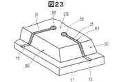
本実施例1の積層型半導体装置1は、図1及び図2に示すように、下段の半導体装置10と、この下段の半導体装置10上に積層される上段の半導体装置40とからなっている。下段の半導体装置10は、各種電子装置の実装基板(配線基板)に実装される外部電極端子を下面に有し、上段の半導体装置40の下面の外部電極端子が接続される端子を上面に有する構造となる。この構造の半導体装置を、説明の便宜上第1の半導体装置10とも呼称する。また、上段の半導体装置40は、外部に露出して設けられる端子は下面の外部電極端子だけである。この構造の半導体装置を、説明の便宜上第2の半導体装置40と呼称する。 As shown in FIGS. 1 and 2, the
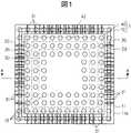
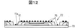
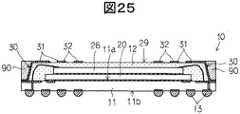
下段の半導体装置(第1の半導体装置)10は、図3乃至図5に示すように、外観的には四角形の配線基板11と、この配線基板11の第1の面11a(図4では上面)に部分的に形成した四角形の封止体12と、配線基板11の第1の面11aの反対面となる第2の面11b(図4では下面)に形成された複数の電極(外部電極端子)13とからなっている。外部電極端子13は、図1及び図2に示すように、四角形の配線基板11の各辺に沿って4列設けられている。 As shown in FIGS. 3 to 5, the lower semiconductor device (first semiconductor device) 10 has a
配線基板11は、例えば、厚さ0.25mmのガラス・エポキシ樹脂配線基板からなり、図4、図5に示すように、第1の面11a及び第2の面11bに所定パターンの配線15,16を有している。これら配線15,16は、図5に示すように、配線基板11の上下面間を貫通する配線17で接続されている。配線基板11の第1の面11a及び第2の面11bには、図示しないが、選択的に絶縁膜(ソルダーレジスト膜)が設けられている。従って、配線基板11の第1の面11a及び第2の面11bには部分的に配線15,16が露出するようになる。第1の面11aに露出する配線15は接続パッド18となり、第2の面11bに露出する配線16は電極(外部電極端子)13を形成するための端子形成パッド19となる。 The
配線基板11の第1の面11aには第1の半導体チップ20が搭載される。第1の半導体チップ20は第1の面及び第1の面の反対面となる第2の面を有し、第1の面に電極(バンプ電極)21を有し、この電極21が一部の接続パッド18にフリップ・チップ接続される(図5参照)。フリップ・チップ接続によって第1の半導体チップ20に形成された図示しない回路素子の各部が接続パッド18に電気的に接続される。フリップ・チップ接続によって第1の半導体チップ20も配線基板11に固定される。図5に示すように、配線基板11と第1の半導体チップ20との間には隙間が存在するが、この隙間には絶縁性樹脂からなるアンダーフィル樹脂22が充填されている。隙間はアンダーフィル樹脂22によって埋め尽くされ、第1の半導体チップ20の第1の面はアンダーフィル樹脂22によって保護される。 A
また、第1の半導体チップ20の第2の面(図4では上面)には絶縁性の接着剤25を介して第2の半導体チップ26が固定される。第2の半導体チップ26は第1の面及び第1の面の反対面となる第2の面を有し、第2の半導体チップ26の第2の面が第1の半導体チップ20に接続される。第2の半導体チップ26の第1の面(図4では上面)には電極27(図5参照)が複数設けられている。これら電極27は四角形の第2の半導体チップ26の各辺の近傍に各辺に沿って設けられている。これら電極27は導電性のワイヤ28によって一部の接続パッド18に電気的に接続されている。 Further, the
封止体12は配線基板11の第1の面11aに選択的に設けられ、第1の半導体チップ20,第2の半導体チップ26及びワイヤ28等を覆う。実施例では、配線基板11の外周部は封止体12の外周縁から外側に突出する構造になっている。封止体12は、トランスファモールディングによって形成される。封止体12は、配線基板11に相似形となる四角形の上面29と、この上面29の各辺に連なり、配線基板11の第1の面11aに到達する傾斜した側面30とからなり、四角形台状の構造になっている。 The sealing
また、封止体12の外周縁から突出する配線基板11部分の第1の面11aには配線15の一部が露出するようになっている(図5参照)。即ち、封止体12から外れた配線基板11部分には配線15が露出している。そして、露出する配線部分には、例えば、銅からなる連結用配線31が重ねて形成されている。この連結用配線31は、配線基板11の第1の面11a上から封止体12の側面30を通り、封止体12の上面29にまで延在している。封止体12の上面29に延在する連結用配線31の先端部分は、図3に示すように、連結用接続パッド32と呼称する円形の端子を形成している。これら連結用接続パッド32上に上段の半導体装置40の下面の外部電極端子が重ねて接続されることになる(図2参照)。なお、連結用接続パッド32は必ずしも円形でなくともよく、四角形等他の形状でもよい。 Further, a part of the
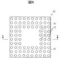
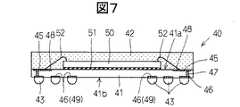
上段の半導体装置(第2の半導体装置)40は、図6及び図7に示すように、外観的には四角形の配線基板41と、この配線基板41の第1の面41a(図7では上面)側に重ねて一致して形成された四角形の封止体42と、配線基板41の第1の面41aの反対面となる第2の面41b(図7では下面)に形成された複数の電極(外部電極端子)43とからなっている。外部電極端子43は、図6に示すように、四角形の配線基板41の各辺に沿って3列設けられている。 As shown in FIGS. 6 and 7, the upper semiconductor device (second semiconductor device) 40 has a
配線基板41は、例えば、厚さ0.25mmのガラス・エポキシ樹脂配線基板からなり、図7に示すように、第1の面41a及び第2の面41bに所定パターンの配線45,46を有している。これら配線45,46は、配線基板41の上下面間を貫通する配線47で接続されている。配線基板41の第1の面41a及び第2の面41bには、図示しないが、選択的に絶縁膜(ソルダーレジスト膜)が設けられている。従って、配線基板41の第1の面41a及び第2の面41bには部分的に配線45,46が露出するようになる。第1の面41aに露出する配線45は接続パッド48となり、第2の面41bに露出する配線46は電極(外部電極端子)43を形成するための端子形成パッド49となる。 The
配線基板41の第1の面41aには半導体チップ50が絶縁性の接着剤51を介して固定されている。半導体チップ50は第1の面(図7では上面)に図示しない電極を有している。この電極と配線基板41の接続パッド48は導電性のワイヤ52によって電気的に接続されている。 A
このような上段の半導体装置40は、図2に示すように、下段の半導体装置10に積層されて積層型半導体装置1となる。即ち、上段の半導体装置40の外部電極端子43が下段の半導体装置10の封止体12の上面29に位置する連結用配線31の連結用接続パッド32に重ねて接続されることによって積層型半導体装置1が製造される。上段の半導体装置40の外部電極端子43は、例えば、半田ボール(Sn−Ag−Cu)で形成されている。従って、下段の半導体装置10上に上段の半導体装置40を位置決めして重ね、半田をリフローして一次的に溶融することによって、外部電極端子43は連結用接続パッド32に接続される。 Such an
つぎに、図8乃至図18を参照しながら積層型半導体装置1の製造方法について説明する。図8は上段の半導体装置40の製造方法を示す図であり、図9は下段の半導体装置10の製造方法の一部を示す図である。図10は下段の半導体装置10の製造方法の一部と、下段の半導体装置10上に上段の半導体装置40を積層して積層型半導体装置1を製造する方法を示す図である。 Next, a method for manufacturing the stacked
最初に、図8(a)〜(f)を参照しながら、上段の半導体装置(第2の半導体装置)40の製造方法について説明する。 First, a method for manufacturing the upper semiconductor device (second semiconductor device) 40 will be described with reference to FIGS.
図8(a)に示すように、配線基板からなる配線母基板60を準備する。配線母基板60は、区画され、矩形枠状の枠部61と、この枠部61の内側に縦横に整列形成(マトリックス状)された複数の製品形成部62を有している。配線母基板60は、製造の最終段階で製品形成部62の外周縁に沿って縦横に切断され、各製品形成部62は上段の半導体装置40になる。従って、配線母基板60は切断によって配線基板41になる。製品形成部62の構造は、既に図6及び図7で説明した配線基板41の構造そのものであることから、製品形成部62の構造説明は省略する。図8(a)では製品形成部62は小さな四角形で示してある。また、配線母基板60の第1の面は配線基板41の第1の面41aであり、同様に製品形成部62の第1の面も配線基板41の第1の面41aである。従って、配線母基板60及び製品形成部62の第1の面及び第2の面を、第1の面41a,第2の面41bとして説明する。 As shown in FIG. 8A, a
つぎに、図8(b)に示すように、各製品形成部62の第1の面41aの所定位置に半導体チップ50を固定する。半導体チップ50は第1の面に図示しない電極を有していることから、第1の面の反対面となる第2の面を絶縁性の接着剤51を介して配線母基板60の第1の面41aに固定する。なお、図8(b)〜(e)において、隣接する一対の一点鎖線間が製品形成部62である。 Next, as shown in FIG. 8B, the
つぎに、図8(c)に示すように、各製品形成部62において、半導体チップ50の第1の面の図示しない電極と配線母基板60の第1の面41aの接続パッド48をワイヤ52で電気的に接続する。 Next, as shown in FIG. 8C, in each
つぎに、図8(d)に示すように、一括モールドを行い、配線母基板60の枠部61の内側領域全体に絶縁性の樹脂からなる封止体42を形成する。封止体42は、例えば、トランスファモールディング装置を使用して形成する。 Next, as shown in FIG. 8D, batch molding is performed to form a sealing
つぎに、図8(e)に示すように、配線母基板60の各製品形成部62の第2の面41bの端子形成パッド49に外部電極端子43を重ねて形成する。外部電極端子43は、例えば、直径250μmの半田ボールで形成したバンプ電極となる。バンプ電極の状態では、外部電極端子43は150μmの厚さになる。 Next, as shown in FIG. 8 (e), the
つぎに、配線母基板60及び封止体42を各製品形成部62の境界線で切断して個片化し、複数の上段の半導体装置40を製造する。配線母基板60は切断によって配線基板41になる。 Next, the
下段の半導体装置(第1の半導体装置)10の製造においては、最初に、図9(a)に示すように、配線基板からなる配線母基板70を準備する。また、第1の面及びその反対面となる第2の面を有し前記第1の面にフリップ・チップ接続用の電極を有する第1の半導体チップと、第1の面及びその反対面となる第2の面を有し前記第1の面にワイヤ接続用の電極を有する第2の半導体チップも準備される。 In manufacturing the lower semiconductor device (first semiconductor device) 10, first, as shown in FIG. 9A, a
配線母基板70は、区画され、矩形枠状の枠部71と、この枠部71の内側に縦横に整列形成(マトリックス状)された複数の製品形成部72を有している。配線母基板70は、製造の最終段階で製品形成部72の外周縁に沿って縦横に切断され、各製品形成部72は下段の半導体装置10になる。従って、配線母基板70は切断によって配線基板11になる。製品形成部72の構造は、既に図3乃至図5で説明した配線基板11の構造そのものであることから、製品形成部72の構造説明は省略する。図9(a)では製品形成部72は小さな四角形で示してある。また、配線母基板70の第1の面は配線基板11の第1の面11aであり、同様に製品形成部72の第1の面も配線基板11の第1の面11aである。従って、配線母基板70及び製品形成部72の第1の面及び第2の面を、第1の面11a,第2の面11bとして説明する。 The
つぎに、図9(b)に示すように、各製品形成部72の第1の面11aの所定位置に第1の半導体チップ20を搭載する。第1の半導体チップ20はフリップ・チップ接続構造となることから、第1の半導体チップ20の電極21は配線母基板70の各製品形成部72の第1の面11aの接続パッド18にフリップ・チップ接続される(図5参照)。また、フリップ・チップボンディング後、配線母基板70と第1の半導体チップ20との間の隙間に絶縁性の樹脂を充填し、かつ樹脂のキュアーを行って樹脂(アンダーフィル樹脂22)で前記隙間を塞ぐ(図5参照)。なお、図9(b)〜(e)及び図10(a),(b)において、隣接する一対の一点鎖線間が製品形成部72である。 Next, as shown in FIG. 9B, the
つぎに、図9(c)に示すように、第2の半導体チップ26を第2の面を介して第1の半導体チップ20の第2の面に絶縁性の接着剤25で接続する。 Next, as shown in FIG. 9C, the
つぎに、図9(d)に示すように、第2の半導体チップ26の電極(図5に示す電極27)と第1の半導体チップ20から外れた位置にある配線母基板70に設けられた接続パッド18(図5参照)を導電性のワイヤ28で接続する。ワイヤ28のループ高さは、第2の半導体チップ26の上面から100μm以下と低くして下段の半導体装置10の高さを極力低くするように配慮されている。実施例では、第2の半導体チップ26は第1の半導体チップ20よりも小さく、全体が第1の半導体チップ20の外周縁よりも内側に位置しているが、第2の半導体チップ26の電極にワイヤを接続するときに支障がなければ、第2の半導体チップ26の外周縁は第1の半導体チップ20の外周縁よりも突出するようなサイズの第2の半導体チップ26であってもよい。 Next, as shown in FIG. 9 (d), the electrode (the
つぎに、図9(e)に示すように、配線母基板70の各製品形成部72の第1の面11aに独立した封止体12を形成する。封止体12は絶縁性の樹脂で形成され、第1の半導体チップ20,第2の半導体チップ26及びワイヤ28等を覆う。封止体12は、例えば、トランスファモールディング装置を用いて形成する。このトランスファモールディング装置におけるモールド金型の封止体12を形成するキャビティ(窪み)には、個々にキャビティの底部分から樹脂が注入されて封止体12が形成される。この封止体12は、露出した部分が、上面29と、この上面29に連なり製品形成部72の第1の面11aに至る傾斜した側面30とからなっている。また、製品形成部72の第1の面11aの配線15の一部は封止体12から外れて露出している。 Next, as shown in FIG. 9E, the
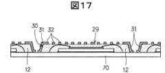
つぎに、図10(a)に示すように、各製品形成部72において、製品形成部72の第1の面11aから封止体12の側面30及び上面29まで延在する連結用配線31を形成する。この連結用配線31は、図5に示すように、封止体12から外れて露出した前記配線15に重なり電気的に接続されている。封止体12の上面29に延在する連結用配線31の先端部分は連結用接続パッド32(図3参照)となっている。この連結用接続パッド32上は、上段の半導体装置40の下面の外部電極端子43が重ねて接続される端子となっている。 Next, as shown in FIG. 10A, in each
つぎに、図10(b)に示すように、配線母基板70の各製品形成部72の第2の面11bの端子形成パッド19に外部電極端子13を重ねて形成する。外部電極端子13は、例えば、直径250μmの半田ボールで形成したバンプ電極となる。バンプ電極の状態では、外部電極端子13は200μmの厚さになる。 Next, as shown in FIG. 10B, the
つぎに、配線母基板70を各製品形成部72の境界線で切断して個片化し、図10(c)に示すように、複数の下段の半導体装置10を製造する。配線母基板70は切断によって配線基板11になる。 Next, the
つぎに、図10(d)に示すように、下段の半導体装置10の上に上段の半導体装置40を位置決めする。その後、下段の半導体装置10の上に上段の半導体装置40を重ね、かつ上段の半導体装置40の外部電極端子43を一時的に加熱処理(リフロー)して下段の半導体装置10の封止体12の上面29の連結用接続パッド32に接続する。これにより、図10(e)に示すような積層型半導体装置1が製造される。 Next, as shown in FIG. 10D, the
ここで、連結用配線31の形成方法について、図11乃至図18を参照しながら説明する。図11は下段の半導体装置10の製造において、配線母基板70に封止体12を形成した状態を示す製品形成部72の平面図である。四角形の封止体12の周辺からそれぞれ突出して描かれる線が配線15である。 Here, a method for forming the
つぎに、配線母基板70の第1の面11aにマスク75を形成する。図12は封止体12上等にマスク75を形成した状態の配線母基板70の製品形成部72を示す断面図であり、図13は平面図である。図12では、マスク75は黒く描かれていて、封止体12の表面及び配線母基板70の第1の面11a上に位置している。このマスク75は、一枚の金属板(Al、SUS等)をパターニングしかつ成形して封止体12の表面及び第1の面11aに密着できる構造になっている。図13では、円とその円に連なる太い線の部分が貫通孔(スリット)76である。この各スリット76が各連結用配線31と一致するパターンとなっている。図14に製品形成部72の角部を拡大して示す。ハッチング部分がマスク75であり、太い黒の点線が配線15である。図14では、スリット76は円形部分と直線部分とからなり、外郭線で示してある。また、図面が見にくくなることから省略してあるが、スリット76の直線部分の先端部分は配線15に重なっている。 Next, a
つぎに、図15に示すように、配線母基板70の製品形成部72の第1の面11a全域上に、金属粒子(例えば、銅の粒子)を含むインク77をインクジェットノズル78で均一に塗布して(吹き付けて)、均一の厚さのインク層79を形成する。図16は図15に示す配線母基板70部分に塗布されたインク層79を示す平面図である。 Next, as shown in FIG. 15, an
つぎに、スリット76に充填されたインク層79の形状を損なうことのないようにマスク75を配線母基板70から取り外す。 Next, the
つぎに、配線母基板70及び封止体12の表面に残留したインク層79を硬化処理する。硬化処理は、例えば、160〜170℃の温度で30分処理する。この硬化処理によって、インクに含まれるバインダー等の有機成分が除去されて導体層が形成され、図17に示すように、連結用配線31が形成される。封止体12の上面29から側面30を通り、製品形成部72の第1の面11aに至って延在する連結用接続パッド32は、図5及び図18に示すように、配線15に重なり電気的に接続される構造になる。これにより、封止体12の外側に露出する各配線15は各連結用配線31によって封止体12の上面に引き出されるため、封止体12の上面29の連結用接続パッド32が各配線15の引き出し端子となる。なお、図12、図15、図17では配線15は省略してある。 Next, the
実施例1によれば、以下の効果を有する。
(1)下段の半導体装置10においては、封止体12を設けた配線基板11の上面(第1の面11a)の一部の配線15は封止体12から外れて露出し、この露出した配線15に電気的に接続される連結用配線31が封止体12の上面29上にまで延在して位置している。そして、封止体12の上面29上の各連結用配線部分(連結用接続パッド32)に、上段の半導体装置40の下面(配線基板41の第2の面41b)の電極(外部電極端子)43が電気的に接続される構造となっている。下段の半導体装置10の封止体12内に複数の半導体チップ(例えば、第1の半導体チップ20及び第2の半導体チップ26)を重ねて搭載すると必然的に封止体12の厚さ(高さ)が厚く(高く)なる。しかし、上段の半導体装置40の電極(外部電極端子)43の厚さ(高さ)は、下段の半導体装置10の封止体12の上面29に設けた連結用配線部分(連結用接続パッド32)に重ねて接続する構造であることから、下段の半導体装置10の封止体12の厚さに左右されることなく薄くできる。この結果、積層型半導体装置1の薄型化が達成できる。上段の半導体装置40の電極(外部電極端子)43は、例えば、半田ボール等によって形成するバンプ電極であるが、この半田ボールも、200〜300μm直径程度にすることができるため、積層型半導体装置1の薄型化が可能になる。Example 1 has the following effects.
(1) In the
(2)下段の半導体装置10において、封止体12を設けた配線基板11の上面(第1の面11a)の一部の配線15を封止体12から外れて露出させるため、配線基板11の外周部は封止体12の外側に突出する構造になる。封止体12の外周縁から突出する配線基板11の突出長さは、配線基板11に設ける配線15と連結用配線31とを電気的に接続するためでよいことから、バンプ電極を配置する構造に比較して前記配線基板外周部分の突出長さは短くでき、積層型半導体装置1の小型化が達成できる。 (2) In the
(3)上記(1)及び(2)により、積層型半導体装置1の小型・薄型化が達成できることになる。 (3) By the above (1) and (2), the
(4)下段の半導体装置10及び上段の半導体装置40には、それぞれ複数の半導体チップを積層して搭載できることから、高密度・高集積度の積層型半導体装置1となる。 (4) Since a plurality of semiconductor chips can be stacked and mounted on the
(5)下段の半導体装置10では、封止体12の上面29に上段の半導体装置40との接続を行う接続部分(連結用配線部分:連結用接続パッド32)を配置する構造であることから、接続部分の配置に制約がなくなり、積層型半導体装置1の設計の自由度が高くなる。 (5) The
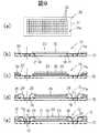
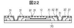
図19乃至図23は本発明の実施例2の積層型半導体装置の製造方法に係わるである。実施例2は、実施例1の積層型半導体装置の製造方法において、下段の半導体装置10の連結用配線31を形成する他の方法に係わるものである。即ち、連結用配線31の封止体12と重なる部分は、封止体12の側面30から上面29に亘って設けられた溝81内に形成されている。図19では、封止体12の側面30から上面29に亘って設けた溝81を示し、図23では、溝81に埋め込まれた連結用配線31を示す。封止体12の上面29の円形部分が連結用接続パッド32となる。 19 to 23 relate to a method for manufacturing a stacked semiconductor device according to the second embodiment of the present invention. The second embodiment relates to another method of forming the
このような構造の下段の半導体装置10は、その製造時、トランスファモールディングによる封止体12の形成工程では、樹脂が充填されるキャビティの壁面に連結用配線に対応する突条が設けられたモールド金型を使用する。図20に示すように、トランスファモールディングにおいては、下型82と上型83とからなるモールド金型84を使用する。この際、封止体12を形成するキャビティ(窪み)85を有する上型83において、連結用配線31を形成したい部分に突条86を設けておく。これにより、図21に示すように、封止体12の側面30及び上面29に選択的に溝81が形成される。 In the manufacturing process of the sealing
つぎに、ディスペンサのノズル87を操作して、溝81に金属粒子を含むインク77を充填する。その後、実施例1と同様にインク77を硬化処理することによって、図22及び図23に示すように、溝81内に連結用配線31を形成する。 Next, the
この実施例によれば、溝81内にインク77を入れて連結用配線31を形成することから、精度良く連結用配線31を形成することができる。また、封止体12と重なる連結用配線31が封止体12の側面30から上面29に亘って設けられた溝81内に形成されていることから、封止体12の上面29に突出する連結用配線31の突出高さ(厚さ)を実施例1の下段の半導体装置10の場合よりも薄くできるため、さらに積層型半導体装置1の薄型化が達成できる。 According to this embodiment, since the connecting
図24は本発明の実施例3の積層型半導体装置の製造方法によって製造された第1の半導体装置を示す平面図である。また、図25は図24のD−D線に沿う断面図である。 FIG. 24 is a plan view showing a first semiconductor device manufactured by the method for manufacturing a stacked semiconductor device according to the third embodiment of the present invention. FIG. 25 is a cross-sectional view taken along the line DD of FIG.
実施例3の積層型半導体装置における下段の半導体装置10は、実施例1の下段の半導体装置10において、図24及び図25に示すように、封止体12の側面30から配線基板11の外周縁に至る配線基板11の第1の面11a側には連結用配線31部分を覆う絶縁性樹脂からなる保護層90が形成されていることを特徴とする。 The
このような下段の半導体装置10は、図10(a)〜(c)に示す実施例1の下段の半導体装置10の製造方法において、図10(b)に示すように、連結用配線31を形成した後、配線母基板70の各製品形成部72の封止体12の外周部分に絶縁性の樹脂を封止体12の高さと同じ程度に埋め込んで保護層90を形成する。つぎに、外部電極端子13を形成し、ついで配線母基板70を保護層90共々切断することによって、図24及び図25に示す下段の半導体装置10を製造する。 Such a
実施例3によれば、下段の半導体装置10において、封止体12の側面30に位置する連結用配線31部分は保護層90によって保護されていることから、配線15及び連結用配線31に異物が付着して発生するショート不良を防止できるため、信頼性が高い積層型半導体装置1となる。 According to the third embodiment, in the
図26は本発明の実施例4である積層型半導体装置の製造方法によって製造された積層型半導体装置を示す断面図である。 FIG. 26 is a cross-sectional view showing a stacked semiconductor device manufactured by a stacked semiconductor device manufacturing method that is Embodiment 4 of the present invention.
実施例4の積層型半導体装置1は、実施例1の積層型半導体装置1において、下段の半導体装置10の第1の半導体チップ20の図示しない電極が配線基板11の配線15(接続パッド18)にワイヤ28によって接続される構造となっている。電極がワイヤ28によって配線15に接続する構造となることから、第1の半導体チップ20の第2の面が絶縁性の接着剤25を介して配線基板11に固定される。また、第2の半導体チップ26は第2の面が絶縁性の接着剤25によって第1の半導体チップ20の第1の面に接続される構造となる。 The
このように、下段の半導体装置10において、配線基板11に搭載する二つの半導体チップの電極の配線との接続を行う接続手段は、フリップ・チップ接続及びワイヤ接続のどちらも採用可能である。また、上段の半導体装置40においても、2個以上の半導体チップを重ねて搭載することも可能である。この場合においても、フリップ・チップ接続及びワイヤ接続のどちらも採用可能である。 As described above, in the
図27は本発明の実施例5である積層型半導体装置の断面図である。実施例5の積層型半導体装置1は、半導体装置をさらに多数積層する構造であり、実施例では3個の半導体装置を積層した例である。 FIG. 27 is a cross-sectional view of a stacked semiconductor device that is Embodiment 5 of the present invention. The
半導体装置を3段以上重ねる構造においては、最下段の半導体装置と、最上段の半導体装置との間に1乃至複数の中段の半導体装置を積層配置するものである。最下段の半導体装置は実施例1の場合の下段の半導体装置(第1の半導体装置)10である。また、最上段の半導体装置は実施例1の場合の上段の半導体装置(第2の半導体装置)40である。中段の半導体装置(第3の半導体装置)95は、寸法等一部は異なるが、実施例1の場合の下段の半導体装置と構成は同じである。従って、中段の半導体装置(第3の半導体装置)95の各部の名称及び符号は下段の半導体装置(第1の半導体装置)10と同じとする。 In a structure in which three or more semiconductor devices are stacked, one or a plurality of middle semiconductor devices are stacked between the lowermost semiconductor device and the uppermost semiconductor device. The lowermost semiconductor device is the lower semiconductor device (first semiconductor device) 10 in the first embodiment. The uppermost semiconductor device is the upper semiconductor device (second semiconductor device) 40 in the first embodiment. The middle semiconductor device (third semiconductor device) 95 is partially different in dimensions and the like, but has the same configuration as the lower semiconductor device in the first embodiment. Accordingly, the names and symbols of the respective parts of the middle semiconductor device (third semiconductor device) 95 are the same as those of the lower semiconductor device (first semiconductor device) 10.
中段の半導体装置(第3の半導体装置)95の下面側の外部電極端子13は、第3の半導体装置95の下方の半導体装置の連結用接続パッド32に重ねて接続され、第3の半導体装置95の封止体12の上面29の連結用接続パッド32には上方の半導体装置の下面側の外部電極端子が重ねて接続される構造となる。 The
中段の半導体装置(第3の半導体装置)95は、封止体12の上面29に連結用接続パッド32を有する構造となるが、この連結用接続パッド32は封止体12の側面30から上面29に亘って設けられる連結用配線31によって形成される構造であることから、上段になればなるほど半導体装置は小型になっていく。 The middle-stage semiconductor device (third semiconductor device) 95 has a structure having a
実施例5によれば、さらに高密度でかつ高集積度の積層型半導体装置を提供することができる。 According to the fifth embodiment, it is possible to provide a stacked semiconductor device with higher density and higher integration.
以上本発明者によってなされた発明を実施例に基づき具体的に説明したが、本発明は上記実施例に限定されるものではなく、その要旨を逸脱しない範囲で種々変更可能であることはいうまでもない。 The invention made by the present inventor has been specifically described based on the embodiments. However, the present invention is not limited to the above embodiments, and various modifications can be made without departing from the scope of the invention. Nor.
例えば、実施例では、下段の半導体装置10の製造において、封止体12は、各製品形成部72の外周部分を枠状に露出させる独立した封止体構造としたが、隣接する製品形成部のキャビティ(窪み)を順次樹脂が流れるトランスファモールディング方法によって封止体を形成する方法でもよい。図28及び図29は製造後の下段の半導体装置10の平面図であるが、封止体12の形成時点では、矢印96に示す方向から樹脂を流入させて封止体12を形成し、矢印97に示す方向に樹脂を流して隣接する製品形成部に封止体を形成する。この樹脂の流入側及び流出側の流路で硬化した樹脂部分98,99は一定の厚さを有することから、この部分をクランプすることによって配線母基板70をクランプすることができる。 For example, in the embodiment, in the manufacture of the
1…積層型半導体装置、10…下段の半導体装置(第1の半導体装置)、11…配線基板、a…第1の面11、11b…第2の面、12…封止体、13…外部電極端子、15,16,17…配線、18…接続パッド18、20…第1の半導体チップ、21…電極、22…接着剤、25…接着剤、26…第2の半導体チップ、27…電極、28…ワイヤ、29…上面、30…側面、31…連結用配線、32…連結用接続パッド、40…上段の半導体装置(第2の半導体装置)、41…配線基板、41a…第1の面、41b…第2の面、42…封止体、43…電極(外部電極端子)、45,46,47…配線、48…接続パッド、49…端子形成パッド、50…半導体チップ、51…接着剤、52…ワイヤ、60…配線母基板、61…枠部、62…製品形成部、70…配線母基板、71…枠部、72…製品形成部、75…マスク、76…貫通孔、77…インク、78…インクジェットノズル、79…インク層、81…溝、82…下型、83…上型、84…モールド金型、85…キャビティ(窪み)、86…突条、87…ノズル、90…保護層、95…中段の半導体装置(第3の半導体装置)、96,97…矢印、98,99…樹脂部分。
DESCRIPTION OF
Claims (21)
Translated fromJapanese前記配線基板の前記第1の面に搭載されかつ電極が接続手段を介して前記配線基板の前記配線に電気的に接続される少なくとも一つの半導体チップと、
前記配線基板の前記第1の面に形成されかつ前記半導体チップ及び前記接続手段を覆う絶縁性樹脂からなる封止体と、
前記配線基板の前記第2の面の前記配線に重ねて形成される複数の電極とを有する二つの半導体装置を2段に積層してなる積層型半導体装置であって、
下段の前記半導体装置にあっては、
前記配線基板の前記第1の面の所定の前記配線に一部が接続され、他の一部が前記封止体の表面に露出する連結用配線を複数有し、
上段の前記半導体装置にあっては、
前記各電極は前記下段の半導体装置の前記各連結用配線の露出する前記他の一部に重なって電気的に接続されていることを特徴とする積層型半導体装置。The first surface and a second surface opposite to the first surface have wiring of a predetermined pattern, and a part of the wiring of the first and second surfaces is the first surface and the second surface. A wiring board connected by wiring penetrating between the two surfaces;
At least one semiconductor chip mounted on the first surface of the wiring board and having an electrode electrically connected to the wiring of the wiring board via connection means;
A sealing body made of an insulating resin that is formed on the first surface of the wiring board and covers the semiconductor chip and the connection means;
A stacked semiconductor device in which two semiconductor devices having a plurality of electrodes formed on the wiring on the second surface of the wiring board are stacked in two stages;
In the lower semiconductor device,
A plurality of connection wirings, a part of which is connected to the predetermined wiring on the first surface of the wiring board and the other part is exposed on the surface of the sealing body;
In the upper semiconductor device,
Each of the electrodes is electrically connected so as to overlap the other exposed part of the connection wiring of the lower semiconductor device.
前記配線基板の前記第1の面に搭載されかつ電極が接続手段を介して前記配線基板の前記配線に電気的に接続される少なくとも一つの半導体チップと、
前記配線基板の前記第1の面に形成されかつ前記半導体チップ及び前記接続手段を覆う絶縁性樹脂からなる封止体と、
前記配線基板の前記第2の面の前記配線に重ねて形成される複数の電極とを有する二つの半導体装置を2段に積層してなる積層型半導体装置であって、
下段の前記半導体装置にあっては、
前記封止体は前記配線基板の一部に形成されて上面と前記上面に連なり前記第1の面に至る側面とを有する構造となり、
前記配線基板の前記第1の面の前記配線の一部は前記封止体から外れて露出し、
前記配線基板の前記第1の面から前記封止体の前記側面及び前記上面まで延在し、かつ前記封止体から外れて露出した前記配線に電気的に接続される連結用配線を複数有し、
上段の前記半導体装置にあっては、
前記各電極は前記下段の半導体装置の前記上面に位置する前記各連結用配線部分に重なって電気的に接続されていることを特徴とする積層型半導体装置。The first surface and a second surface opposite to the first surface have wiring of a predetermined pattern, and a part of the wiring of the first and second surfaces is the first surface and the second surface. A wiring board connected by wiring penetrating between the two surfaces;
At least one semiconductor chip mounted on the first surface of the wiring board and having an electrode electrically connected to the wiring of the wiring board via connection means;
A sealing body made of an insulating resin that is formed on the first surface of the wiring board and covers the semiconductor chip and the connection means;
A stacked semiconductor device in which two semiconductor devices having a plurality of electrodes formed on the wiring on the second surface of the wiring board are stacked in two stages;
In the lower semiconductor device,
The sealing body is formed on a part of the wiring board and has a structure having an upper surface and a side surface extending to the upper surface and reaching the first surface,
A portion of the wiring on the first surface of the wiring substrate is exposed off the sealing body;
There are a plurality of connection wirings extending from the first surface of the wiring board to the side surface and the upper surface of the sealing body and electrically connected to the wiring exposed off the sealing body. And
In the upper semiconductor device,
Each of the electrodes overlaps with each of the connecting wiring portions located on the upper surface of the lower semiconductor device, and is electrically connected.
前記配線基板の前記第1の面に搭載されかつ電極が接続手段を介して前記配線基板の前記配線に電気的に接続される少なくとも一つの半導体チップと、
前記配線基板の前記第1の面に形成されかつ前記半導体チップ及び前記接続手段を覆う絶縁性樹脂からなる封止体と、
前記配線基板の前記第2の面の前記配線に重ねて形成される複数の電極とを有する二つの半導体装置を2段に積層してなる積層型半導体装置であって、
下段の前記半導体装置にあっては、
前記封止体は前記配線基板の一部に形成されて上面と前記上面に連なり前記第1の面に至る側面とを有する構造となり、
前記配線基板の前記第1の面の前記配線の一部は前記封止体から外れて露出し、
前記配線基板の前記第1の面から前記封止体の前記側面及び前記上面まで延在し、かつ前記封止体から外れて露出した前記配線に電気的に接続される連結用配線を複数有し、
前記封止体の側面から前記配線基板の外周縁に至る前記配線基板の前記第1の面側には前記連結用配線部分を覆う絶縁性樹脂からなる保護層が形成され、
上段の前記半導体装置にあっては、
前記各電極は前記下段の半導体装置の前記上面に位置する前記各連結用配線部分に重なって電気的に接続されていることを特徴とする積層型半導体装置。The first surface and a second surface opposite to the first surface have wiring of a predetermined pattern, and a part of the wiring of the first and second surfaces is the first surface and the second surface. A wiring board connected by wiring penetrating between the two surfaces;
At least one semiconductor chip mounted on the first surface of the wiring board and having an electrode electrically connected to the wiring of the wiring board via connection means;
A sealing body made of an insulating resin that is formed on the first surface of the wiring board and covers the semiconductor chip and the connection means;
A stacked semiconductor device in which two semiconductor devices having a plurality of electrodes formed on the wiring on the second surface of the wiring board are stacked in two stages;
In the lower semiconductor device,
The sealing body is formed on a part of the wiring board and has a structure having an upper surface and a side surface extending to the upper surface and reaching the first surface,
A portion of the wiring on the first surface of the wiring substrate is exposed off the sealing body;
There are a plurality of connection wirings extending from the first surface of the wiring board to the side surface and the upper surface of the sealing body and electrically connected to the wiring exposed off the sealing body. And
A protective layer made of an insulating resin covering the connecting wiring portion is formed on the first surface side of the wiring board from the side surface of the sealing body to the outer periphery of the wiring board,
In the upper semiconductor device,
Each of the electrodes overlaps with each of the connecting wiring portions located on the upper surface of the lower semiconductor device, and is electrically connected.
下段の前記半導体装置は、
(a)第1の面及びこの第1の面の反対面となる第2の面を有し、前記第1の面に複数の電極を有する半導体チップを準備する工程、
(b)第1の面及びこの第1の面の反対面となる第2の面に所定パターンの配線を有し、前記第1及び第2の面の前記配線の一部は前記第1の面及び第2の面間を貫通する配線で接続されてなる製品形成部を縦横に整列形成し、
前記製品形成部の前記第1の面の前記配線は前記半導体チップの前記各電極に接続手段を介して電気的に接続される各接続パッドを有し、
前記製品形成部の前記第2の面の前記配線は端子形成パッドを複数有する配線母基板を準備する工程、
(c)前記配線母基板の前記各製品形成部の前記第1の面に前記半導体チップを搭載し、かつ前記半導体チップの前記各電極を接続手段を介して前記各接続パッドに電気的に接続する工程、
(d)前記配線母基板の前記各製品形成部の前記第1の面に、前記第1の面の前記配線の一部を露出させたままとし、前記半導体チップ及び前記接続手段を覆い、上面と前記上面に連なり前記製品形成部の前記第1の面に至る側面とを有する絶縁性の樹脂からなる封止体を形成する工程、
(e)前記配線母基板の前記各製品形成部の前記第1の面上から前記封止体の前記側面及び前記上面上まで延在し、かつ前記封止体から外れて露出した前記配線の一部に電気的に接続される連結用配線を複数形成する工程、
(f)前記配線母基板の前記各製品形成部の前記第2の面の前記端子形成パッドに外部電極端子を形成する工程、
(g)前記配線母基板を前記各製品形成部の境界線で切断して個片化する工程、
によって製造し、
上段の前記半導体装置は、
(h)第1の面及びこの第1の面の反対面となる第2の面を有し、前記第1の面に複数の電極を有する半導体チップを準備する工程、
(i)第1の面及びこの第1の面の反対面となる第2の面に所定パターンの配線を有し、前記第1及び第2の面の前記配線の一部は前記第1の面及び第2の面間を貫通する配線で接続されてなる製品形成部を縦横に整列形成し、
前記製品形成部の前記第1の面の前記配線は前記半導体チップの前記各電極に接続手段を介して電気的に接続される各接続パッドを有し、
前記製品形成部の前記第2の面の前記配線は前記下段の半導体装置の前記封止体の前記上面上の前記連結用配線部分に対応するように設けられた端子形成パッドを複数有する配線母基板を準備する工程、
(j)前記配線母基板の前記各製品形成部の前記第1の面に前記半導体チップを搭載し、かつ前記半導体チップの前記各電極を接続手段を介して前記接続パッドに電気的に接続する工程、
(k)前記配線母基板の前記各製品形成部の前記第1の面に前記半導体チップ及び前記接続手段を覆う絶縁性の樹脂からなる封止体を形成する工程、
(l)前記配線母基板の前記各製品形成部の前記第2の面の前記端子形成パッドに外部電極端子を形成する工程、
(m)前記配線母基板または前記配線母基板と前記封止体を前記各製品形成部の境界線で切断して個片化する工程、
によって製造し、
(n)前記下段の半導体装置の前記封止体の前記上面に位置する前記各連結用配線部分上に、前記上段の半導体装置の前記外部電極端子を重ね、前記外部電極端子と前記連結用配線部分を接続させる工程、
によって、二つの半導体装置を2段に積層した積層型半導体装置を製造することを特徴とする積層型半導体装置の製造方法。A method of manufacturing a stacked semiconductor device by stacking two semiconductor devices in two stages,
The lower semiconductor device is
(A) preparing a semiconductor chip having a first surface and a second surface opposite to the first surface, and having a plurality of electrodes on the first surface;
(B) A wiring having a predetermined pattern is provided on the first surface and a second surface opposite to the first surface, and a part of the wiring on the first and second surfaces is the first surface. Product forming portions connected by wiring penetrating between the surface and the second surface are formed vertically and horizontally,
The wiring on the first surface of the product forming portion has connection pads electrically connected to the electrodes of the semiconductor chip via connection means,
A step of preparing a wiring mother board having a plurality of terminal forming pads for the wiring on the second surface of the product forming portion;
(C) The semiconductor chip is mounted on the first surface of each product forming portion of the wiring motherboard, and the electrodes of the semiconductor chip are electrically connected to the connection pads via connection means. The process of
(D) A part of the wiring on the first surface is left exposed on the first surface of each product forming portion of the wiring motherboard, covering the semiconductor chip and the connecting means, and an upper surface And forming a sealing body made of an insulating resin having a side surface extending to the upper surface and reaching the first surface of the product forming portion,
(E) the wiring extending from the first surface of each product forming portion of the wiring motherboard to the side surface and the upper surface of the sealing body and exposed outside the sealing body; Forming a plurality of connecting wires that are electrically connected to a part;
(F) forming an external electrode terminal on the terminal forming pad on the second surface of each product forming portion of the wiring motherboard;
(G) A step of cutting the wiring mother board at a boundary line of each of the product forming portions into pieces.
Manufactured by and
The upper semiconductor device is
(H) preparing a semiconductor chip having a first surface and a second surface opposite to the first surface, and having a plurality of electrodes on the first surface;
(I) wiring having a predetermined pattern is provided on the first surface and a second surface opposite to the first surface, and a part of the wiring on the first and second surfaces is the first surface; Product forming portions connected by wiring penetrating between the surface and the second surface are formed vertically and horizontally,
The wiring on the first surface of the product forming portion has connection pads electrically connected to the electrodes of the semiconductor chip via connection means,
A wiring mother having a plurality of terminal forming pads provided so that the wiring on the second surface of the product forming portion corresponds to the connecting wiring portion on the upper surface of the sealing body of the lower semiconductor device. Preparing a substrate,
(J) The semiconductor chip is mounted on the first surface of each product forming portion of the wiring motherboard, and the electrodes of the semiconductor chip are electrically connected to the connection pads via connection means. Process,
(K) forming a sealing body made of an insulating resin that covers the semiconductor chip and the connecting means on the first surface of each of the product forming portions of the wiring motherboard;
(L) forming an external electrode terminal on the terminal forming pad on the second surface of each product forming portion of the wiring motherboard;
(M) A step of cutting the wiring mother board or the wiring mother board and the sealing body into pieces by cutting at a boundary line between the product forming portions,
Manufactured by and
(N) The external electrode terminal of the upper semiconductor device is overlaid on each connection wiring portion located on the upper surface of the sealing body of the lower semiconductor device, and the external electrode terminal and the connection wiring Connecting the parts,
To manufacture a stacked semiconductor device in which two semiconductor devices are stacked in two stages.
(1)前記配線母基板の前記各製品形成部の前記第1の面上に、前記第1の面及び前記封止体の前記側面及び前記上面に密着して重なるように屈曲し、かつ前記連結用配線に対応するスリットが設けられた一枚のマスクを重ねる工程と、
(2)前記配線母基板の前記各製品形成部の前記第1の面全域上に、金属粒子を含むインクを均一の厚さに塗布する工程と、
(3)前記配線母基板から前記マスクの前記スリットに充填された前記インクの形状を損なうことのないように前記マスクを取り外す工程と、
(4)前記配線母基板及び前記封止体に残留した前記インクを硬化処理する工程と、
によって、前記連結用配線を形成することを特徴とする請求項9に記載の積層型半導体装置の製造方法。In the step of forming the connection wiring in the step (e),
(1) The first surface of each product forming portion of the wiring mother board is bent so as to be in close contact with the first surface, the side surface and the upper surface of the sealing body, and A step of overlaying one mask provided with slits corresponding to the connection wiring;
(2) A step of applying an ink containing metal particles to a uniform thickness over the entire first surface of each product forming portion of the wiring mother board;
(3) removing the mask from the wiring motherboard so as not to impair the shape of the ink filled in the slit of the mask;
(4) a step of curing the ink remaining on the wiring motherboard and the sealing body;
The method for manufacturing a stacked semiconductor device according to claim 9, wherein the connecting wiring is formed by:
前記樹脂が充填されるキャビティの壁面に前記連結用配線に対応する突条が設けられたモールド金型を用いて前記封止体を形成して、前記封止体の前記側面及び前記上面に選択的に溝を形成し、
前記工程(e)の連結用配線の形成工程では、
前記封止体の表面に設けられた溝に金属粒子を含むインクを充填し、
前記インクを硬化処理することによって、前記連結用配線を形成することを特徴とする請求項9に記載の積層型半導体装置の製造方法。In the step of forming the sealing body in the step (d),
The sealing body is formed using a mold die provided with protrusions corresponding to the connecting wiring on the wall surface of the cavity filled with the resin, and the side surface and the upper surface of the sealing body are selected. Forming grooves,
In the step of forming the connection wiring in the step (e),
Filling the groove provided on the surface of the sealing body with ink containing metal particles,
The method for manufacturing a stacked semiconductor device according to claim 9, wherein the connecting wiring is formed by curing the ink.
(1)第1の面及びその反対面となる第2の面を有し前記第1の面にフリップ・チップ接続用の電極を有する第1の半導体チップと、第1の面及びその反対面となる第2の面を有し前記第1の面にワイヤ接続用の電極を有する第2の半導体チップを準備し、
(2)前記配線母基板の前記各製品形成部の前記接続パッドに前記電極を介して前記第1の半導体チップをフリップ・チップ接続し、
(3)前記第2の半導体チップを第2の面を介して前記第1の半導体チップの前記第2の面に絶縁性接着剤で接続し、
(4)前記第2の半導体チップの前記電極と前記第1の半導体チップから外れた位置にある前記接続パッドを導電性のワイヤで接続することを特徴とする請求項9に記載の積層型半導体装置の製造方法。In the mounting step of the semiconductor chip in the step (c),
(1) a first semiconductor chip having a first surface and a second surface opposite to the first surface, and having an electrode for flip chip connection on the first surface, and the first surface and the opposite surface A second semiconductor chip having a second surface and a wire connecting electrode on the first surface;
(2) The first semiconductor chip is flip-chip connected to the connection pads of the product forming portions of the wiring mother board via the electrodes.
(3) connecting the second semiconductor chip to the second surface of the first semiconductor chip through a second surface with an insulating adhesive;
(4) The stacked semiconductor according to claim 9, wherein the electrode of the second semiconductor chip is connected to the connection pad at a position away from the first semiconductor chip with a conductive wire. Device manufacturing method.
(1)第1の面及びその反対面となる第2の面を有し前記第1の面の周縁にワイヤ接続用の電極を有する第1の半導体チップと、第1の面及びその反対面となる第2の面を有し前記第1の面にワイヤ接続用の電極を有しかつ前記第1の半導体チップに重ねたとき前記第1の半導体チップの前記電極が露出する大きさである第2の半導体チップを準備し、
(2)前記配線母基板の前記各製品形成部の前記第1の面に前記第1の前記半導体チップを第2の面を介して絶縁性の接着剤で接続し、
(3)前記第1の半導体チップの前記電極を露出させる状態で前記第2の半導体チップを第2の面を介して前記第1の半導体チップ20の第1の面に絶縁性の接着剤で固定し、
(4)前記第1及び第2の半導体チップの前記各電極と前記各接続パッドを導電性のワイヤで接続することを特徴とする請求項9に記載の積層型半導体装置の製造方法。In the mounting step of the semiconductor chip in the step (c),
(1) A first semiconductor chip having a first surface and a second surface which is the opposite surface, and having a wire connection electrode on the periphery of the first surface, and the first surface and the opposite surface The first surface has a wire-connecting electrode, and the electrode of the first semiconductor chip is exposed when the first surface is overlaid on the first semiconductor chip. Preparing a second semiconductor chip,
(2) The first semiconductor chip is connected to the first surface of each of the product forming portions of the wiring motherboard by an insulating adhesive via a second surface;
(3) The second semiconductor chip is exposed to the first surface of the first semiconductor chip 20 with an insulating adhesive through the second surface in a state where the electrodes of the first semiconductor chip are exposed. Fixed,
(4) The method for manufacturing a stacked semiconductor device according to (9), wherein the electrodes and the connection pads of the first and second semiconductor chips are connected by a conductive wire.
下段の前記半導体装置は、
(a)第1の面及びこの第1の面の反対面となる第2の面を有し、前記第1の面に複数の電極を有する半導体チップを準備する工程、
(b)第1の面及びこの第1の面の反対面となる第2の面に所定パターンの配線を有し、前記第1及び第2の面の前記配線の一部は前記第1の面及び第2の面間を貫通する配線で接続されてなる製品形成部を縦横に整列形成し、
前記製品形成部の前記第1の面の前記配線は前記半導体チップの前記各電極に接続手段を介して電気的に接続される各接続パッドを有し、
前記製品形成部の前記第2の面の前記配線は端子形成パッドを複数有する配線母基板を準備する工程、
(c)前記配線母基板の前記各製品形成部の前記第1の面に前記半導体チップを搭載し、かつ前記半導体チップの前記各電極を接続手段を介して前記各接続パッドに電気的に接続する工程、
(d)前記配線母基板の前記各製品形成部の前記第1の面に、前記第1の面の前記配線の一部を露出させたままとし、前記半導体チップ及び前記接続手段を覆い、上面と前記上面に連なり前記製品形成部の前記第1の面に至る側面とを有する絶縁性の樹脂からなる封止体を形成する工程、
(e)前記配線母基板の前記各製品形成部の前記第1の面上から前記封止体の前記側面及び前記上面上まで延在し、かつ前記封止体から外れて露出した前記配線の一部に電気的に接続される連結用配線を複数形成する工程、
(f)前記配線母基板の前記各製品形成部の前記第1の面において、前記封止体の側面から前記製品形成部の外周縁に至る部分に前記連結用配線部分を覆う絶縁性樹脂からなる保護層を形成する工程、
(g)前記配線母基板の前記各製品形成部の前記第2の面の前記端子形成パッドに外部電極端子を形成する工程、
(h)前記配線母基板を前記各製品形成部の境界線で切断して個片化する工程、
によって製造し、
上段の前記半導体装置は、
(i)第1の面及びこの第1の面の反対面となる第2の面を有し、前記第1の面に複数の電極を有する半導体チップを準備する工程、
(j)第1の面及びこの第1の面の反対面となる第2の面に所定パターンの配線を有し、前記第1及び第2の面の前記配線の一部は前記第1の面及び第2の面間を貫通する配線で接続されてなる製品形成部を縦横に整列形成し、
前記製品形成部の前記第1の面の前記配線は前記半導体チップの前記各電極に接続手段を介して電気的に接続される各接続パッドを有し、
前記製品形成部の前記第2の面の前記配線は前記下段の半導体装置の前記封止体の前記上面上の前記連結用配線部分に対応するように設けられた端子形成パッドを複数有する配線母基板を準備する工程、
(k)前記配線母基板の前記各製品形成部の前記第1の面に前記半導体チップを搭載し、かつ前記半導体チップの前記各電極を接続手段を介して前記接続パッドに電気的に接続する工程、
(l)前記配線母基板の前記各製品形成部の前記第1の面に前記半導体チップ及び前記接続手段を覆う絶縁性の樹脂からなる封止体を形成する工程、
(m)前記配線母基板の前記各製品形成部の前記第2の面の前記端子形成パッドに外部電極端子を形成する工程、
(n)前記配線母基板または前記配線母基板と前記封止体を前記各製品形成部の境界線で切断して個片化する工程、
によって製造し、
(o)前記下段の半導体装置の前記封止体の前記上面に位置する前記各連結用配線部分上に、前記上段の半導体装置の前記外部電極端子を重ね、前記外部電極端子と前記連結用配線部分を接続させる工程、
によって、二つの半導体装置を2段に積層した積層型半導体装置を製造することを特徴とする積層型半導体装置の製造方法。A method of manufacturing a stacked semiconductor device by stacking two semiconductor devices in two stages,
The lower semiconductor device is
(A) preparing a semiconductor chip having a first surface and a second surface opposite to the first surface, and having a plurality of electrodes on the first surface;
(B) A wiring having a predetermined pattern is provided on the first surface and a second surface opposite to the first surface, and a part of the wiring on the first and second surfaces is the first surface. Product forming portions connected by wiring penetrating between the surface and the second surface are formed vertically and horizontally,
The wiring on the first surface of the product forming portion has connection pads electrically connected to the electrodes of the semiconductor chip via connection means,
A step of preparing a wiring mother board having a plurality of terminal forming pads for the wiring on the second surface of the product forming portion;
(C) The semiconductor chip is mounted on the first surface of each product forming portion of the wiring motherboard, and the electrodes of the semiconductor chip are electrically connected to the connection pads via connection means. The process of
(D) A part of the wiring on the first surface is left exposed on the first surface of each product forming portion of the wiring motherboard, covering the semiconductor chip and the connecting means, and an upper surface And forming a sealing body made of an insulating resin having a side surface extending to the upper surface and reaching the first surface of the product forming portion,
(E) the wiring extending from the first surface of each product forming portion of the wiring mother board to the side surface and the upper surface of the sealing body and exposed outside the sealing body; Forming a plurality of connecting wires that are electrically connected to a part;
(F) In the first surface of each product forming portion of the wiring mother board, from an insulating resin that covers the connecting wiring portion from the side surface of the sealing body to the outer peripheral edge of the product forming portion. Forming a protective layer,
(G) forming an external electrode terminal on the terminal forming pad on the second surface of each product forming portion of the wiring motherboard;
(H) A step of cutting the wiring mother board at a boundary line between the product forming parts to separate the wiring mother board;
Manufactured by and
The upper semiconductor device is
(I) preparing a semiconductor chip having a first surface and a second surface opposite to the first surface, and having a plurality of electrodes on the first surface;
(J) A wiring having a predetermined pattern is provided on the first surface and a second surface opposite to the first surface, and a part of the wiring on the first and second surfaces is the first surface. Product forming portions connected by wiring penetrating between the surface and the second surface are formed vertically and horizontally,
The wiring on the first surface of the product forming portion has connection pads electrically connected to the electrodes of the semiconductor chip via connection means,
A wiring mother having a plurality of terminal forming pads provided so that the wiring on the second surface of the product forming portion corresponds to the connecting wiring portion on the upper surface of the sealing body of the lower semiconductor device. Preparing a substrate,
(K) The semiconductor chip is mounted on the first surface of each product forming portion of the wiring motherboard, and the electrodes of the semiconductor chip are electrically connected to the connection pads via connection means. Process,
(L) forming a sealing body made of an insulating resin that covers the semiconductor chip and the connection means on the first surface of each product forming portion of the wiring motherboard;
(M) forming an external electrode terminal on the terminal forming pad on the second surface of each product forming portion of the wiring motherboard;
(N) A step of cutting the wiring mother board or the wiring mother board and the sealing body into pieces by cutting at the boundary lines of the respective product forming parts,
Manufactured by and
(O) The external electrode terminal of the upper semiconductor device is overlaid on each connection wiring portion positioned on the upper surface of the sealing body of the lower semiconductor device, and the external electrode terminal and the connection wiring Connecting the parts,
To manufacture a stacked semiconductor device in which two semiconductor devices are stacked in two stages.
(1)前記配線母基板の前記各製品形成部の前記第1の面上に、前記第1の面及び前記封止体の前記側面及び前記上面に密着して重なるように屈曲し、かつ前記連結用配線に対応するスリットが設けられた一枚のマスクを重ねる工程と、
(2)前記配線母基板の前記各製品形成部の前記第1の面全域上に、金属粒子を含むインクを均一の厚さに塗布する工程と、
(3)前記配線母基板から前記マスクの前記スリットに充填された前記インクの形状を損なうことのないように前記マスクを取り外す工程と、
(4)前記配線母基板及び前記封止体に残留した前記インクを硬化処理する工程と、
によって、前記連結用配線を形成することを特徴とする請求項14に記載の積層型半導体装置の製造方法。In the step of forming the connection wiring in the step (e),
(1) The first surface of each product forming portion of the wiring mother board is bent so as to be in close contact with the first surface, the side surface and the upper surface of the sealing body, and A step of overlaying one mask provided with slits corresponding to the connection wiring;
(2) A step of applying an ink containing metal particles to a uniform thickness over the entire first surface of each product forming portion of the wiring mother board;
(3) removing the mask from the wiring motherboard so as not to impair the shape of the ink filled in the slit of the mask;
(4) a step of curing the ink remaining on the wiring motherboard and the sealing body;
The method of manufacturing a stacked semiconductor device according to claim 14, wherein the connecting wiring is formed by:
前記樹脂が充填されるキャビティの壁面に前記連結用配線に対応する突条が設けられたモールド金型を用いて前記封止体を形成して、前記封止体の前記側面及び前記上面に選択的に溝を形成し、
前記工程(e)の連結用配線の形成工程では、
前記封止体の表面に設けられた溝に金属粒子を含むインクを充填し、
前記インクを硬化処理することによって、前記連結用配線を形成することを特徴とする請求項14に記載の積層型半導体装置の製造方法。In the step of forming the sealing body in the step (d),
The sealing body is formed using a mold die provided with protrusions corresponding to the connecting wiring on the wall surface of the cavity filled with the resin, and the side surface and the upper surface of the sealing body are selected. Forming grooves,
In the step of forming the connection wiring in the step (e),
Filling the groove provided on the surface of the sealing body with ink containing metal particles,
15. The method for manufacturing a stacked semiconductor device according to claim 14, wherein the connecting wiring is formed by curing the ink.
(1)第1の面及びその反対面となる第2の面を有し前記第1の面にフリップ・チップ接続用の電極を有する第1の半導体チップと、第1の面及びその反対面となる第2の面を有し前記第1の面にワイヤ接続用の電極を有する第2の半導体チップを準備し、
(2)前記配線母基板の前記各製品形成部の前記接続パッドに前記電極を介して前記第1の半導体チップをフリップ・チップ接続し、
(3)前記第2の半導体チップを第2の面を介して前記第1の半導体チップの前記第2の面に絶縁性接着剤で接続し、
(4)前記第2の半導体チップの前記電極と前記第1の半導体チップから外れた位置にある前記接続パッドを導電性のワイヤで接続することを特徴とする請求項14に記載の積層型半導体装置の製造方法。In the mounting step of the semiconductor chip in the step (c),
(1) a first semiconductor chip having a first surface and a second surface opposite to the first surface, and having an electrode for flip chip connection on the first surface, and the first surface and the opposite surface A second semiconductor chip having a second surface and a wire connecting electrode on the first surface;
(2) The first semiconductor chip is flip-chip connected to the connection pads of the product forming portions of the wiring mother board via the electrodes.
(3) connecting the second semiconductor chip to the second surface of the first semiconductor chip through a second surface with an insulating adhesive;
(4) The stacked semiconductor according to (14), wherein the electrode of the second semiconductor chip and the connection pad at a position away from the first semiconductor chip are connected by a conductive wire. Device manufacturing method.
(1)第1の面及びその反対面となる第2の面を有し前記第1の面の周縁にワイヤ接続用の電極を有する第1の半導体チップと、第1の面及びその反対面となる第2の面を有し前記第1の面にワイヤ接続用の電極を有しかつ前記第1の半導体チップに重ねたとき前記第1の半導体チップの前記電極が露出する大きさである第2の半導体チップを準備し、
(2)前記配線母基板の前記各製品形成部の前記第1の面に前記第1の前記半導体チップを第2の面を介して絶縁性の接着剤で接続し、
(3)前記第1の半導体チップの前記電極を露出させる状態で前記第2の半導体チップを第2の面を介して前記第1の半導体チップ20の第1の面に絶縁性の接着剤で固定し、
(4)前記第1及び第2の半導体チップの前記各電極と前記各接続パッドを導電性のワイヤで接続することを特徴とする請求項14に記載の積層型半導体装置の製造方法。In the mounting step of the semiconductor chip in the step (c),
(1) A first semiconductor chip having a first surface and a second surface which is the opposite surface, and having a wire connection electrode on the periphery of the first surface, and the first surface and the opposite surface The first surface has a wire-connecting electrode, and the electrode of the first semiconductor chip is exposed when the first surface is overlaid on the first semiconductor chip. Preparing a second semiconductor chip,
(2) The first semiconductor chip is connected to the first surface of each of the product forming portions of the wiring motherboard by an insulating adhesive via a second surface;
(3) The second semiconductor chip is exposed to the first surface of the first semiconductor chip 20 with an insulating adhesive through the second surface in a state where the electrodes of the first semiconductor chip are exposed. Fixed,
(4) The method for manufacturing a stacked semiconductor device according to (14), wherein the electrodes and the connection pads of the first and second semiconductor chips are connected by a conductive wire.
前記配線基板の前記第1の面に搭載されかつ電極が接続手段を介して前記配線基板の前記配線に電気的に接続される半導体チップと、
前記配線基板の前記第1の面に形成されかつ前記半導体チップ及び前記接続手段を覆う絶縁性樹脂からなる封止体と、
前記配線基板の前記第2の面の前記配線に重ねて形成される複数の電極とを有する3個以上の半導体装置を多段に積層してなる積層型半導体装置であって、
下段と上段との関係にある下段の半導体装置及び上段の半導体装置において、
前記下段の半導体装置は、前記配線基板の前記第1の面の所定の前記配線に一部が接続され、他の一部が前記封止体の表面に露出する連結用配線を複数有し、
前記上段の半導体装置は、前記各電極が前記下段の半導体装置の前記封止体の表面に露出する前記各連結用配線部分に重なって電気的に接続されていることを特徴とする積層型半導体装置。The first surface and a second surface opposite to the first surface have wiring of a predetermined pattern, and a part of the wiring of the first and second surfaces is the first surface and the second surface. A wiring board connected by wiring penetrating between the two surfaces;
A semiconductor chip mounted on the first surface of the wiring board and having an electrode electrically connected to the wiring of the wiring board via connection means;
A sealing body made of an insulating resin that is formed on the first surface of the wiring board and covers the semiconductor chip and the connection means;
A stacked semiconductor device in which three or more semiconductor devices having a plurality of electrodes formed on the wiring on the second surface of the wiring substrate are stacked in multiple stages,
In the lower semiconductor device and the upper semiconductor device in the relationship between the lower and upper stages,
The lower-stage semiconductor device has a plurality of connection wirings that are partially connected to the predetermined wiring on the first surface of the wiring board and the other part exposed on the surface of the sealing body,
The upper semiconductor device is characterized in that each electrode is electrically connected so as to overlap each of the connecting wiring portions exposed on the surface of the sealing body of the lower semiconductor device. apparatus.
前記配線基板の前記第1の面に搭載されかつ電極が接続手段を介して前記配線基板の前記配線に電気的に接続される半導体チップと、
前記配線基板の前記第1の面に形成されかつ前記半導体チップ及び前記接続手段を覆う絶縁性樹脂からなる封止体と、
前記配線基板の前記第2の面の前記配線に重ねて形成される複数の電極とを有し、
複数の半導体装置を多段に積層する積層型半導体装置の最下段または中段を構成する半導体装置であって、
前記封止体は前記配線基板の一部に形成され、上面と、前記上面に連なり前記第1の面に至る側面とを有する構造となり、
前記配線基板の前記第1の面の前記配線の一部は前記封止体から外れて露出し、
前記配線基板の前記第1の面から前記封止体の前記側面及び前記上面まで延在し、かつ前記封止体から外れて露出した前記配線に電気的に接続される連結用配線を複数有し、
前記連結用配線は、前記積層型半導体装置を構成する最上段の半導体装置の電極または中段を構成する半導体装置の電極が接続される部分となることを特徴とする半導体装置。The first surface and a second surface opposite to the first surface have wiring of a predetermined pattern, and a part of the wiring of the first and second surfaces is the first surface and the second surface. A wiring board connected by wiring penetrating between the two surfaces;
A semiconductor chip mounted on the first surface of the wiring board and having an electrode electrically connected to the wiring of the wiring board via connection means;
A sealing body made of an insulating resin that is formed on the first surface of the wiring board and covers the semiconductor chip and the connection means;
A plurality of electrodes formed to overlap the wiring on the second surface of the wiring board;
A semiconductor device constituting the lowermost or middle stage of a stacked semiconductor device in which a plurality of semiconductor devices are stacked in multiple stages,
The sealing body is formed on a part of the wiring board, and has a structure having an upper surface and a side surface connected to the upper surface and reaching the first surface,
A portion of the wiring on the first surface of the wiring substrate is exposed off the sealing body;
There are a plurality of connection wirings extending from the first surface of the wiring board to the side surface and the upper surface of the sealing body and electrically connected to the wiring exposed off the sealing body. And
2. The semiconductor device according to claim 1, wherein the connection wiring is a portion to which an electrode of the uppermost semiconductor device constituting the stacked semiconductor device or an electrode of the semiconductor device constituting the middle stage is connected.
Priority Applications (5)
| Application Number | Priority Date | Filing Date | Title |
|---|---|---|---|
| JP2006113529AJP5598787B2 (en) | 2006-04-17 | 2006-04-17 | Manufacturing method of stacked semiconductor device |
| US11/734,054US7808093B2 (en) | 2006-04-17 | 2007-04-11 | Stacked semiconductor device |
| TW096112814ATWI352420B (en) | 2006-04-17 | 2007-04-12 | Stacked semiconductor device and fabrication metho |
| US12/875,799US8247896B2 (en) | 2006-04-17 | 2010-09-03 | Stacked semiconductor device and fabrication method for same |
| US13/540,233US9252125B2 (en) | 2006-04-17 | 2012-07-02 | Stacked semiconductor device and fabrication method for same |
Applications Claiming Priority (1)
| Application Number | Priority Date | Filing Date | Title |
|---|---|---|---|
| JP2006113529AJP5598787B2 (en) | 2006-04-17 | 2006-04-17 | Manufacturing method of stacked semiconductor device |
Publications (2)
| Publication Number | Publication Date |
|---|---|
| JP2007287922Atrue JP2007287922A (en) | 2007-11-01 |
| JP5598787B2 JP5598787B2 (en) | 2014-10-01 |
Family
ID=38604066
Family Applications (1)
| Application Number | Title | Priority Date | Filing Date |
|---|---|---|---|
| JP2006113529AExpired - Fee RelatedJP5598787B2 (en) | 2006-04-17 | 2006-04-17 | Manufacturing method of stacked semiconductor device |
Country Status (3)
| Country | Link |
|---|---|
| US (3) | US7808093B2 (en) |
| JP (1) | JP5598787B2 (en) |
| TW (1) | TWI352420B (en) |
Cited By (48)
| Publication number | Priority date | Publication date | Assignee | Title |
|---|---|---|---|---|
| JP2009094434A (en)* | 2007-10-12 | 2009-04-30 | Elpida Memory Inc | Semiconductor device, and manufacturing method of the same |
| JP2013526084A (en)* | 2010-11-15 | 2013-06-20 | テッセラ,インコーポレイテッド | Microelectronic package having terminals on a dielectric mass |
| US8836136B2 (en) | 2011-10-17 | 2014-09-16 | Invensas Corporation | Package-on-package assembly with wire bond vias |
| US8835228B2 (en) | 2012-05-22 | 2014-09-16 | Invensas Corporation | Substrate-less stackable package with wire-bond interconnect |
| US8878353B2 (en) | 2012-12-20 | 2014-11-04 | Invensas Corporation | Structure for microelectronic packaging with bond elements to encapsulation surface |
| US8883563B1 (en) | 2013-07-15 | 2014-11-11 | Invensas Corporation | Fabrication of microelectronic assemblies having stack terminals coupled by connectors extending through encapsulation |
| US8907466B2 (en) | 2010-07-19 | 2014-12-09 | Tessera, Inc. | Stackable molded microelectronic packages |
| US8927337B2 (en) | 2004-11-03 | 2015-01-06 | Tessera, Inc. | Stacked packaging improvements |
| US8975738B2 (en) | 2012-11-12 | 2015-03-10 | Invensas Corporation | Structure for microelectronic packaging with terminals on dielectric mass |
| US9023691B2 (en) | 2013-07-15 | 2015-05-05 | Invensas Corporation | Microelectronic assemblies with stack terminals coupled by connectors extending through encapsulation |
| US9034696B2 (en) | 2013-07-15 | 2015-05-19 | Invensas Corporation | Microelectronic assemblies having reinforcing collars on connectors extending through encapsulation |
| US9082753B2 (en) | 2013-11-12 | 2015-07-14 | Invensas Corporation | Severing bond wire by kinking and twisting |
| US9087815B2 (en) | 2013-11-12 | 2015-07-21 | Invensas Corporation | Off substrate kinking of bond wire |
| US9093435B2 (en) | 2011-05-03 | 2015-07-28 | Tessera, Inc. | Package-on-package assembly with wire bonds to encapsulation surface |
| US9159708B2 (en) | 2010-07-19 | 2015-10-13 | Tessera, Inc. | Stackable molded microelectronic packages with area array unit connectors |
| US9214454B2 (en) | 2014-03-31 | 2015-12-15 | Invensas Corporation | Batch process fabrication of package-on-package microelectronic assemblies |
| US9218988B2 (en) | 2005-12-23 | 2015-12-22 | Tessera, Inc. | Microelectronic packages and methods therefor |
| US9224717B2 (en) | 2011-05-03 | 2015-12-29 | Tessera, Inc. | Package-on-package assembly with wire bonds to encapsulation surface |
| US9324681B2 (en) | 2010-12-13 | 2016-04-26 | Tessera, Inc. | Pin attachment |
| US9349706B2 (en) | 2012-02-24 | 2016-05-24 | Invensas Corporation | Method for package-on-package assembly with wire bonds to encapsulation surface |
| US9391008B2 (en) | 2012-07-31 | 2016-07-12 | Invensas Corporation | Reconstituted wafer-level package DRAM |
| US9412714B2 (en) | 2014-05-30 | 2016-08-09 | Invensas Corporation | Wire bond support structure and microelectronic package including wire bonds therefrom |
| US9502390B2 (en) | 2012-08-03 | 2016-11-22 | Invensas Corporation | BVA interposer |
| US9583411B2 (en) | 2014-01-17 | 2017-02-28 | Invensas Corporation | Fine pitch BVA using reconstituted wafer with area array accessible for testing |
| US9601454B2 (en) | 2013-02-01 | 2017-03-21 | Invensas Corporation | Method of forming a component having wire bonds and a stiffening layer |
| US9646917B2 (en) | 2014-05-29 | 2017-05-09 | Invensas Corporation | Low CTE component with wire bond interconnects |
| US9659848B1 (en) | 2015-11-18 | 2017-05-23 | Invensas Corporation | Stiffened wires for offset BVA |
| US9685365B2 (en) | 2013-08-08 | 2017-06-20 | Invensas Corporation | Method of forming a wire bond having a free end |
| US9691679B2 (en) | 2012-02-24 | 2017-06-27 | Invensas Corporation | Method for package-on-package assembly with wire bonds to encapsulation surface |
| US9728527B2 (en) | 2013-11-22 | 2017-08-08 | Invensas Corporation | Multiple bond via arrays of different wire heights on a same substrate |
| US9735084B2 (en) | 2014-12-11 | 2017-08-15 | Invensas Corporation | Bond via array for thermal conductivity |
| US9761554B2 (en) | 2015-05-07 | 2017-09-12 | Invensas Corporation | Ball bonding metal wire bond wires to metal pads |
| US9812402B2 (en) | 2015-10-12 | 2017-11-07 | Invensas Corporation | Wire bond wires for interference shielding |
| US9842745B2 (en) | 2012-02-17 | 2017-12-12 | Invensas Corporation | Heat spreading substrate with embedded interconnects |
| US9852969B2 (en) | 2013-11-22 | 2017-12-26 | Invensas Corporation | Die stacks with one or more bond via arrays of wire bond wires and with one or more arrays of bump interconnects |
| US9888579B2 (en) | 2015-03-05 | 2018-02-06 | Invensas Corporation | Pressing of wire bond wire tips to provide bent-over tips |
| US9911718B2 (en) | 2015-11-17 | 2018-03-06 | Invensas Corporation | ‘RDL-First’ packaged microelectronic device for a package-on-package device |
| US9935075B2 (en) | 2016-07-29 | 2018-04-03 | Invensas Corporation | Wire bonding method and apparatus for electromagnetic interference shielding |
| US9984992B2 (en) | 2015-12-30 | 2018-05-29 | Invensas Corporation | Embedded wire bond wires for vertical integration with separate surface mount and wire bond mounting surfaces |
| US10008477B2 (en) | 2013-09-16 | 2018-06-26 | Invensas Corporation | Microelectronic element with bond elements to encapsulation surface |
| US10008469B2 (en) | 2015-04-30 | 2018-06-26 | Invensas Corporation | Wafer-level packaging using wire bond wires in place of a redistribution layer |
| US10026717B2 (en) | 2013-11-22 | 2018-07-17 | Invensas Corporation | Multiple bond via arrays of different wire heights on a same substrate |
| US10181457B2 (en) | 2015-10-26 | 2019-01-15 | Invensas Corporation | Microelectronic package for wafer-level chip scale packaging with fan-out |
| US10299368B2 (en) | 2016-12-21 | 2019-05-21 | Invensas Corporation | Surface integrated waveguides and circuit structures therefor |
| US10332854B2 (en) | 2015-10-23 | 2019-06-25 | Invensas Corporation | Anchoring structure of fine pitch bva |
| US10381326B2 (en) | 2014-05-28 | 2019-08-13 | Invensas Corporation | Structure and method for integrated circuits packaging with increased density |
| US10460958B2 (en) | 2013-08-07 | 2019-10-29 | Invensas Corporation | Method of manufacturing embedded packaging with preformed vias |
| US10490528B2 (en) | 2015-10-12 | 2019-11-26 | Invensas Corporation | Embedded wire bond wires |
Families Citing this family (38)
| Publication number | Priority date | Publication date | Assignee | Title |
|---|---|---|---|---|
| US8471374B2 (en)* | 2006-02-21 | 2013-06-25 | Stats Chippac Ltd. | Integrated circuit package system with L-shaped leadfingers |
| JP5598787B2 (en)* | 2006-04-17 | 2014-10-01 | マイクロンメモリジャパン株式会社 | Manufacturing method of stacked semiconductor device |
| US8841759B2 (en)* | 2006-12-23 | 2014-09-23 | Lg Innotek Co., Ltd. | Semiconductor package and manufacturing method thereof |
| JP2009044110A (en)* | 2007-08-13 | 2009-02-26 | Elpida Memory Inc | Semiconductor device and its manufacturing method |
| US7834464B2 (en)* | 2007-10-09 | 2010-11-16 | Infineon Technologies Ag | Semiconductor chip package, semiconductor chip assembly, and method for fabricating a device |
| JP2009105139A (en)* | 2007-10-22 | 2009-05-14 | Shinko Electric Ind Co Ltd | Wiring board and manufacturing method thereof, and semiconductor device |
| US8212339B2 (en) | 2008-02-05 | 2012-07-03 | Advanced Semiconductor Engineering, Inc. | Semiconductor device packages with electromagnetic interference shielding |
| US8350367B2 (en) | 2008-02-05 | 2013-01-08 | Advanced Semiconductor Engineering, Inc. | Semiconductor device packages with electromagnetic interference shielding |
| US7480426B1 (en)* | 2008-03-25 | 2009-01-20 | International Business Machines Corporation | Method of forming a three-dimensional stacked optical device |
| US7477811B1 (en)* | 2008-03-25 | 2009-01-13 | International Business Machines Corporation | Method of forming a three-dimensional stacked optical device |
| JP5543084B2 (en)* | 2008-06-24 | 2014-07-09 | ピーエスフォー ルクスコ エスエイアールエル | Manufacturing method of semiconductor device |
| US8410584B2 (en) | 2008-08-08 | 2013-04-02 | Advanced Semiconductor Engineering, Inc. | Semiconductor device packages with electromagnetic interference shielding |
| US8110902B2 (en)* | 2009-02-19 | 2012-02-07 | Advanced Semiconductor Engineering, Inc. | Chip package and manufacturing method thereof |
| TWI379367B (en)* | 2009-06-15 | 2012-12-11 | Kun Yuan Technology Co Ltd | Chip packaging method and structure thereof |
| US8212340B2 (en) | 2009-07-13 | 2012-07-03 | Advanced Semiconductor Engineering, Inc. | Chip package and manufacturing method thereof |
| US8030750B2 (en)* | 2009-11-19 | 2011-10-04 | Advanced Semiconductor Engineering, Inc. | Semiconductor device packages with electromagnetic interference shielding |
| US8368185B2 (en) | 2009-11-19 | 2013-02-05 | Advanced Semiconductor Engineering, Inc. | Semiconductor device packages with electromagnetic interference shielding |
| US8378466B2 (en) | 2009-11-19 | 2013-02-19 | Advanced Semiconductor Engineering, Inc. | Wafer-level semiconductor device packages with electromagnetic interference shielding |
| US8569894B2 (en) | 2010-01-13 | 2013-10-29 | Advanced Semiconductor Engineering, Inc. | Semiconductor package with single sided substrate design and manufacturing methods thereof |
| TWI411075B (en) | 2010-03-22 | 2013-10-01 | Advanced Semiconductor Eng | Semiconductor package and manufacturing method thereof |
| US9406658B2 (en) | 2010-12-17 | 2016-08-02 | Advanced Semiconductor Engineering, Inc. | Embedded component device and manufacturing methods thereof |
| KR101678969B1 (en)* | 2011-03-09 | 2016-11-23 | 테세라, 인코포레이티드 | Microelectronic package with terminals on dielectric mass |
| US8692377B2 (en) | 2011-03-23 | 2014-04-08 | Stats Chippac Ltd. | Integrated circuit packaging system with plated leads and method of manufacture thereof |
| US8530277B2 (en)* | 2011-06-16 | 2013-09-10 | Stats Chippac Ltd. | Integrated circuit packaging system with package on package support and method of manufacture thereof |
| KR101831692B1 (en) | 2011-08-17 | 2018-02-26 | 삼성전자주식회사 | Semiconductor Devices, Package Substrates, Semiconductor Packages, Package Stack Structures, and Electronic Systems having Functionally Asymmetric Conductive elements |
| US9548283B2 (en)* | 2012-07-05 | 2017-01-17 | Taiwan Semiconductor Manufacturing Company, Ltd. | Package redistribution layer structure and method of forming same |
| TWI581396B (en) | 2012-10-17 | 2017-05-01 | 環旭電子股份有限公司 | Three-dimensional stacked package structure and manufacturing method thereof |
| CN203026500U (en)* | 2012-12-25 | 2013-06-26 | 华为终端有限公司 | Stack packaging device |
| US9385070B2 (en) | 2013-06-28 | 2016-07-05 | Delta Electronics, Inc. | Semiconductor component having a lateral semiconductor device and a vertical semiconductor device |
| CN104576411A (en)* | 2013-10-25 | 2015-04-29 | 飞思卡尔半导体公司 | Top gateway mold with double corners |
| US9202789B2 (en)* | 2014-04-16 | 2015-12-01 | Qualcomm Incorporated | Die package comprising die-to-wire connector and a wire-to-die connector configured to couple to a die package |
| US10685943B2 (en) | 2015-05-14 | 2020-06-16 | Mediatek Inc. | Semiconductor chip package with resilient conductive paste post and fabrication method thereof |
| US9842831B2 (en) | 2015-05-14 | 2017-12-12 | Mediatek Inc. | Semiconductor package and fabrication method thereof |
| FR3041209B1 (en)* | 2015-09-15 | 2017-09-15 | Sagem Defense Securite | COMPACT ELECTRONIC SYSTEM AND DEVICE COMPRISING SUCH A SYSTEM |
| CN106847802B (en)* | 2016-12-29 | 2019-09-24 | 矽力杰半导体技术(杭州)有限公司 | Optical sensor package component and preparation method thereof and electronic equipment |
| WO2018126542A1 (en)* | 2017-01-04 | 2018-07-12 | 华为技术有限公司 | Pop (package on package) structure and terminal |
| CN109637939B (en)* | 2017-10-09 | 2020-08-18 | 中芯国际集成电路制造(上海)有限公司 | Semiconductor packaging mold, semiconductor device and packaging method of semiconductor device |
| TWI822504B (en)* | 2022-12-05 | 2023-11-11 | 勤誠興業股份有限公司 | Printed circuit board |
Citations (3)
| Publication number | Priority date | Publication date | Assignee | Title |
|---|---|---|---|---|
| JP2004266271A (en)* | 2003-02-12 | 2004-09-24 | Matsushita Electric Ind Co Ltd | Electronic component package and method of manufacturing the same |
| JP2005203497A (en)* | 2004-01-14 | 2005-07-28 | Toshiba Corp | Semiconductor device and manufacturing method thereof |
| JP2005317861A (en)* | 2004-04-30 | 2005-11-10 | Toshiba Corp | Semiconductor device and manufacturing method thereof |
Family Cites Families (17)
| Publication number | Priority date | Publication date | Assignee | Title |
|---|---|---|---|---|
| TW400587B (en) | 1999-01-06 | 2000-08-01 | United Microelectronics Corp | Multi-chip chip scale package |
| US6607937B1 (en)* | 2000-08-23 | 2003-08-19 | Micron Technology, Inc. | Stacked microelectronic dies and methods for stacking microelectronic dies |
| US7443010B2 (en)* | 2001-04-05 | 2008-10-28 | Taiwan Semiconductor Manufacturing Co., Ltd. | Matrix form semiconductor package substrate having an electrode of serpentine shape |
| DE10149689A1 (en)* | 2001-10-09 | 2003-04-10 | Philips Corp Intellectual Pty | Electrical/electronic component has lateral, rear cover materials at least partly of electrically conductive material and/or of electrically conductive material in layers but in connected manner |
| US20040061213A1 (en)* | 2002-09-17 | 2004-04-01 | Chippac, Inc. | Semiconductor multi-package module having package stacked over die-up flip chip ball grid array package and having wire bond interconnect between stacked packages |
| AU2003298595A1 (en) | 2002-10-08 | 2004-05-04 | Chippac, Inc. | Semiconductor stacked multi-package module having inverted second package |
| DE10250538B4 (en) | 2002-10-29 | 2008-02-21 | Infineon Technologies Ag | Electronic component as multichip module and method for its production |
| JP2004172157A (en) | 2002-11-15 | 2004-06-17 | Shinko Electric Ind Co Ltd | Semiconductor package and package stack semiconductor device |
| JP3917946B2 (en) | 2003-03-11 | 2007-05-23 | 富士通株式会社 | Multilayer semiconductor device |
| DE10360708B4 (en) | 2003-12-19 | 2008-04-10 | Infineon Technologies Ag | Semiconductor module with a semiconductor stack, rewiring plate, and method of making the same |
| SG130055A1 (en)* | 2005-08-19 | 2007-03-20 | Micron Technology Inc | Microelectronic devices, stacked microelectronic devices, and methods for manufacturing microelectronic devices |
| JP4473807B2 (en)* | 2005-10-27 | 2010-06-02 | パナソニック株式会社 | Multilayer semiconductor device and lower layer module of multilayer semiconductor device |
| SG133445A1 (en)* | 2005-12-29 | 2007-07-30 | Micron Technology Inc | Methods for packaging microelectronic devices and microelectronic devices formed using such methods |
| US7312519B2 (en)* | 2006-01-12 | 2007-12-25 | Stats Chippac Ltd. | Stacked integrated circuit package-in-package system |
| JP5598787B2 (en) | 2006-04-17 | 2014-10-01 | マイクロンメモリジャパン株式会社 | Manufacturing method of stacked semiconductor device |
| US7550857B1 (en)* | 2006-11-16 | 2009-06-23 | Amkor Technology, Inc. | Stacked redistribution layer (RDL) die assembly package |
| TWI400587B (en) | 2009-12-16 | 2013-07-01 | Ind Tech Res Inst | Biomass chemical toner composition and method for manufacturing the same |
- 2006
- 2006-04-17JPJP2006113529Apatent/JP5598787B2/ennot_activeExpired - Fee Related
- 2007
- 2007-04-11USUS11/734,054patent/US7808093B2/enactiveActive
- 2007-04-12TWTW096112814Apatent/TWI352420B/ennot_activeIP Right Cessation
- 2010
- 2010-09-03USUS12/875,799patent/US8247896B2/ennot_activeExpired - Fee Related
- 2012
- 2012-07-02USUS13/540,233patent/US9252125B2/ennot_activeExpired - Fee Related
Patent Citations (3)
| Publication number | Priority date | Publication date | Assignee | Title |
|---|---|---|---|---|
| JP2004266271A (en)* | 2003-02-12 | 2004-09-24 | Matsushita Electric Ind Co Ltd | Electronic component package and method of manufacturing the same |
| JP2005203497A (en)* | 2004-01-14 | 2005-07-28 | Toshiba Corp | Semiconductor device and manufacturing method thereof |
| JP2005317861A (en)* | 2004-04-30 | 2005-11-10 | Toshiba Corp | Semiconductor device and manufacturing method thereof |
Cited By (97)
| Publication number | Priority date | Publication date | Assignee | Title |
|---|---|---|---|---|
| US9153562B2 (en) | 2004-11-03 | 2015-10-06 | Tessera, Inc. | Stacked packaging improvements |
| US8927337B2 (en) | 2004-11-03 | 2015-01-06 | Tessera, Inc. | Stacked packaging improvements |
| US9570416B2 (en) | 2004-11-03 | 2017-02-14 | Tessera, Inc. | Stacked packaging improvements |
| US9984901B2 (en) | 2005-12-23 | 2018-05-29 | Tessera, Inc. | Method for making a microelectronic assembly having conductive elements |
| US9218988B2 (en) | 2005-12-23 | 2015-12-22 | Tessera, Inc. | Microelectronic packages and methods therefor |
| JP2009094434A (en)* | 2007-10-12 | 2009-04-30 | Elpida Memory Inc | Semiconductor device, and manufacturing method of the same |
| US10128216B2 (en) | 2010-07-19 | 2018-11-13 | Tessera, Inc. | Stackable molded microelectronic packages |
| US9553076B2 (en) | 2010-07-19 | 2017-01-24 | Tessera, Inc. | Stackable molded microelectronic packages with area array unit connectors |
| US9570382B2 (en) | 2010-07-19 | 2017-02-14 | Tessera, Inc. | Stackable molded microelectronic packages |
| US8907466B2 (en) | 2010-07-19 | 2014-12-09 | Tessera, Inc. | Stackable molded microelectronic packages |
| US9123664B2 (en) | 2010-07-19 | 2015-09-01 | Tessera, Inc. | Stackable molded microelectronic packages |
| US9159708B2 (en) | 2010-07-19 | 2015-10-13 | Tessera, Inc. | Stackable molded microelectronic packages with area array unit connectors |
| US8659164B2 (en) | 2010-11-15 | 2014-02-25 | Tessera, Inc. | Microelectronic package with terminals on dielectric mass |
| US8957527B2 (en) | 2010-11-15 | 2015-02-17 | Tessera, Inc. | Microelectronic package with terminals on dielectric mass |
| US8637991B2 (en) | 2010-11-15 | 2014-01-28 | Tessera, Inc. | Microelectronic package with terminals on dielectric mass |
| US8623706B2 (en) | 2010-11-15 | 2014-01-07 | Tessera, Inc. | Microelectronic package with terminals on dielectric mass |
| JP2013526084A (en)* | 2010-11-15 | 2013-06-20 | テッセラ,インコーポレイテッド | Microelectronic package having terminals on a dielectric mass |
| US9324681B2 (en) | 2010-12-13 | 2016-04-26 | Tessera, Inc. | Pin attachment |
| US10062661B2 (en) | 2011-05-03 | 2018-08-28 | Tessera, Inc. | Package-on-package assembly with wire bonds to encapsulation surface |
| US9224717B2 (en) | 2011-05-03 | 2015-12-29 | Tessera, Inc. | Package-on-package assembly with wire bonds to encapsulation surface |
| US9093435B2 (en) | 2011-05-03 | 2015-07-28 | Tessera, Inc. | Package-on-package assembly with wire bonds to encapsulation surface |
| US9691731B2 (en) | 2011-05-03 | 2017-06-27 | Tessera, Inc. | Package-on-package assembly with wire bonds to encapsulation surface |
| US10593643B2 (en) | 2011-05-03 | 2020-03-17 | Tessera, Inc. | Package-on-package assembly with wire bonds to encapsulation surface |
| US11424211B2 (en) | 2011-05-03 | 2022-08-23 | Tessera Llc | Package-on-package assembly with wire bonds to encapsulation surface |
| US9041227B2 (en) | 2011-10-17 | 2015-05-26 | Invensas Corporation | Package-on-package assembly with wire bond vias |
| US9252122B2 (en) | 2011-10-17 | 2016-02-02 | Invensas Corporation | Package-on-package assembly with wire bond vias |
| US9761558B2 (en) | 2011-10-17 | 2017-09-12 | Invensas Corporation | Package-on-package assembly with wire bond vias |
| US8836136B2 (en) | 2011-10-17 | 2014-09-16 | Invensas Corporation | Package-on-package assembly with wire bond vias |
| US11735563B2 (en) | 2011-10-17 | 2023-08-22 | Invensas Llc | Package-on-package assembly with wire bond vias |
| US10756049B2 (en) | 2011-10-17 | 2020-08-25 | Invensas Corporation | Package-on-package assembly with wire bond vias |
| US11189595B2 (en) | 2011-10-17 | 2021-11-30 | Invensas Corporation | Package-on-package assembly with wire bond vias |
| US9842745B2 (en) | 2012-02-17 | 2017-12-12 | Invensas Corporation | Heat spreading substrate with embedded interconnects |
| US9691679B2 (en) | 2012-02-24 | 2017-06-27 | Invensas Corporation | Method for package-on-package assembly with wire bonds to encapsulation surface |
| US9349706B2 (en) | 2012-02-24 | 2016-05-24 | Invensas Corporation | Method for package-on-package assembly with wire bonds to encapsulation surface |
| US10510659B2 (en) | 2012-05-22 | 2019-12-17 | Invensas Corporation | Substrate-less stackable package with wire-bond interconnect |
| US9953914B2 (en) | 2012-05-22 | 2018-04-24 | Invensas Corporation | Substrate-less stackable package with wire-bond interconnect |
| US8835228B2 (en) | 2012-05-22 | 2014-09-16 | Invensas Corporation | Substrate-less stackable package with wire-bond interconnect |
| US10170412B2 (en) | 2012-05-22 | 2019-01-01 | Invensas Corporation | Substrate-less stackable package with wire-bond interconnect |
| US9391008B2 (en) | 2012-07-31 | 2016-07-12 | Invensas Corporation | Reconstituted wafer-level package DRAM |
| US9917073B2 (en) | 2012-07-31 | 2018-03-13 | Invensas Corporation | Reconstituted wafer-level package dram with conductive interconnects formed in encapsulant at periphery of the package |
| US10297582B2 (en) | 2012-08-03 | 2019-05-21 | Invensas Corporation | BVA interposer |
| US9502390B2 (en) | 2012-08-03 | 2016-11-22 | Invensas Corporation | BVA interposer |
| US8975738B2 (en) | 2012-11-12 | 2015-03-10 | Invensas Corporation | Structure for microelectronic packaging with terminals on dielectric mass |
| US9095074B2 (en) | 2012-12-20 | 2015-07-28 | Invensas Corporation | Structure for microelectronic packaging with bond elements to encapsulation surface |
| US8878353B2 (en) | 2012-12-20 | 2014-11-04 | Invensas Corporation | Structure for microelectronic packaging with bond elements to encapsulation surface |
| US9615456B2 (en) | 2012-12-20 | 2017-04-04 | Invensas Corporation | Microelectronic assembly for microelectronic packaging with bond elements to encapsulation surface |
| US9601454B2 (en) | 2013-02-01 | 2017-03-21 | Invensas Corporation | Method of forming a component having wire bonds and a stiffening layer |
| US9633979B2 (en) | 2013-07-15 | 2017-04-25 | Invensas Corporation | Microelectronic assemblies having stack terminals coupled by connectors extending through encapsulation |
| US9023691B2 (en) | 2013-07-15 | 2015-05-05 | Invensas Corporation | Microelectronic assemblies with stack terminals coupled by connectors extending through encapsulation |
| US8883563B1 (en) | 2013-07-15 | 2014-11-11 | Invensas Corporation | Fabrication of microelectronic assemblies having stack terminals coupled by connectors extending through encapsulation |
| US9034696B2 (en) | 2013-07-15 | 2015-05-19 | Invensas Corporation | Microelectronic assemblies having reinforcing collars on connectors extending through encapsulation |
| US10460958B2 (en) | 2013-08-07 | 2019-10-29 | Invensas Corporation | Method of manufacturing embedded packaging with preformed vias |
| US9685365B2 (en) | 2013-08-08 | 2017-06-20 | Invensas Corporation | Method of forming a wire bond having a free end |
| US10008477B2 (en) | 2013-09-16 | 2018-06-26 | Invensas Corporation | Microelectronic element with bond elements to encapsulation surface |
| US9082753B2 (en) | 2013-11-12 | 2015-07-14 | Invensas Corporation | Severing bond wire by kinking and twisting |
| US9087815B2 (en) | 2013-11-12 | 2015-07-21 | Invensas Corporation | Off substrate kinking of bond wire |
| US9893033B2 (en) | 2013-11-12 | 2018-02-13 | Invensas Corporation | Off substrate kinking of bond wire |
| US10290613B2 (en) | 2013-11-22 | 2019-05-14 | Invensas Corporation | Multiple bond via arrays of different wire heights on a same substrate |
| US9728527B2 (en) | 2013-11-22 | 2017-08-08 | Invensas Corporation | Multiple bond via arrays of different wire heights on a same substrate |
| US10629567B2 (en) | 2013-11-22 | 2020-04-21 | Invensas Corporation | Multiple plated via arrays of different wire heights on same substrate |
| USRE49987E1 (en) | 2013-11-22 | 2024-05-28 | Invensas Llc | Multiple plated via arrays of different wire heights on a same substrate |
| US10026717B2 (en) | 2013-11-22 | 2018-07-17 | Invensas Corporation | Multiple bond via arrays of different wire heights on a same substrate |
| US9852969B2 (en) | 2013-11-22 | 2017-12-26 | Invensas Corporation | Die stacks with one or more bond via arrays of wire bond wires and with one or more arrays of bump interconnects |
| US9837330B2 (en) | 2014-01-17 | 2017-12-05 | Invensas Corporation | Fine pitch BVA using reconstituted wafer with area array accessible for testing |
| US10529636B2 (en) | 2014-01-17 | 2020-01-07 | Invensas Corporation | Fine pitch BVA using reconstituted wafer with area array accessible for testing |
| US11404338B2 (en) | 2014-01-17 | 2022-08-02 | Invensas Corporation | Fine pitch bva using reconstituted wafer with area array accessible for testing |
| US9583411B2 (en) | 2014-01-17 | 2017-02-28 | Invensas Corporation | Fine pitch BVA using reconstituted wafer with area array accessible for testing |
| US11990382B2 (en) | 2014-01-17 | 2024-05-21 | Adeia Semiconductor Technologies Llc | Fine pitch BVA using reconstituted wafer with area array accessible for testing |
| US9812433B2 (en) | 2014-03-31 | 2017-11-07 | Invensas Corporation | Batch process fabrication of package-on-package microelectronic assemblies |
| US9356006B2 (en) | 2014-03-31 | 2016-05-31 | Invensas Corporation | Batch process fabrication of package-on-package microelectronic assemblies |
| US9214454B2 (en) | 2014-03-31 | 2015-12-15 | Invensas Corporation | Batch process fabrication of package-on-package microelectronic assemblies |
| US10381326B2 (en) | 2014-05-28 | 2019-08-13 | Invensas Corporation | Structure and method for integrated circuits packaging with increased density |
| US10032647B2 (en) | 2014-05-29 | 2018-07-24 | Invensas Corporation | Low CTE component with wire bond interconnects |
| US10475726B2 (en) | 2014-05-29 | 2019-11-12 | Invensas Corporation | Low CTE component with wire bond interconnects |
| US9646917B2 (en) | 2014-05-29 | 2017-05-09 | Invensas Corporation | Low CTE component with wire bond interconnects |
| US9412714B2 (en) | 2014-05-30 | 2016-08-09 | Invensas Corporation | Wire bond support structure and microelectronic package including wire bonds therefrom |
| US9947641B2 (en) | 2014-05-30 | 2018-04-17 | Invensas Corporation | Wire bond support structure and microelectronic package including wire bonds therefrom |
| US9735084B2 (en) | 2014-12-11 | 2017-08-15 | Invensas Corporation | Bond via array for thermal conductivity |
| US10806036B2 (en) | 2015-03-05 | 2020-10-13 | Invensas Corporation | Pressing of wire bond wire tips to provide bent-over tips |
| US9888579B2 (en) | 2015-03-05 | 2018-02-06 | Invensas Corporation | Pressing of wire bond wire tips to provide bent-over tips |
| US10008469B2 (en) | 2015-04-30 | 2018-06-26 | Invensas Corporation | Wafer-level packaging using wire bond wires in place of a redistribution layer |
| US9761554B2 (en) | 2015-05-07 | 2017-09-12 | Invensas Corporation | Ball bonding metal wire bond wires to metal pads |
| US10115678B2 (en) | 2015-10-12 | 2018-10-30 | Invensas Corporation | Wire bond wires for interference shielding |
| US10490528B2 (en) | 2015-10-12 | 2019-11-26 | Invensas Corporation | Embedded wire bond wires |
| US10559537B2 (en) | 2015-10-12 | 2020-02-11 | Invensas Corporation | Wire bond wires for interference shielding |
| US11462483B2 (en) | 2015-10-12 | 2022-10-04 | Invensas Llc | Wire bond wires for interference shielding |
| US9812402B2 (en) | 2015-10-12 | 2017-11-07 | Invensas Corporation | Wire bond wires for interference shielding |
| US10332854B2 (en) | 2015-10-23 | 2019-06-25 | Invensas Corporation | Anchoring structure of fine pitch bva |
| US10181457B2 (en) | 2015-10-26 | 2019-01-15 | Invensas Corporation | Microelectronic package for wafer-level chip scale packaging with fan-out |
| US10043779B2 (en) | 2015-11-17 | 2018-08-07 | Invensas Corporation | Packaged microelectronic device for a package-on-package device |
| US9911718B2 (en) | 2015-11-17 | 2018-03-06 | Invensas Corporation | ‘RDL-First’ packaged microelectronic device for a package-on-package device |
| US9659848B1 (en) | 2015-11-18 | 2017-05-23 | Invensas Corporation | Stiffened wires for offset BVA |
| US10325877B2 (en) | 2015-12-30 | 2019-06-18 | Invensas Corporation | Embedded wire bond wires for vertical integration with separate surface mount and wire bond mounting surfaces |
| US9984992B2 (en) | 2015-12-30 | 2018-05-29 | Invensas Corporation | Embedded wire bond wires for vertical integration with separate surface mount and wire bond mounting surfaces |
| US10658302B2 (en) | 2016-07-29 | 2020-05-19 | Invensas Corporation | Wire bonding method and apparatus for electromagnetic interference shielding |
| US9935075B2 (en) | 2016-07-29 | 2018-04-03 | Invensas Corporation | Wire bonding method and apparatus for electromagnetic interference shielding |
| US10299368B2 (en) | 2016-12-21 | 2019-05-21 | Invensas Corporation | Surface integrated waveguides and circuit structures therefor |
Also Published As
| Publication number | Publication date |
|---|---|
| TWI352420B (en) | 2011-11-11 |
| US20070241437A1 (en) | 2007-10-18 |
| JP5598787B2 (en) | 2014-10-01 |
| US8247896B2 (en) | 2012-08-21 |
| US9252125B2 (en) | 2016-02-02 |
| TW200810079A (en) | 2008-02-16 |
| US7808093B2 (en) | 2010-10-05 |
| US20130001755A1 (en) | 2013-01-03 |
| US20110001235A1 (en) | 2011-01-06 |
Similar Documents
| Publication | Publication Date | Title |
|---|---|---|
| JP5598787B2 (en) | Manufacturing method of stacked semiconductor device | |
| CN108091615B (en) | Semiconductor package | |
| JP6027966B2 (en) | Stackable mold microelectronic package with area array unit connector | |
| KR100800478B1 (en) | Multilayer semiconductor package and manufacturing method thereof | |
| US8253232B2 (en) | Package on package having a conductive post with height lower than an upper surface of an encapsulation layer to prevent circuit pattern lift defect and method of fabricating the same | |
| US20090045497A1 (en) | Semiconductor device and method of manufacturing the same | |
| US20080160678A1 (en) | Method for fabricating semiconductor package | |
| CN112768437B (en) | Multilayer stack packaging structure and preparation method thereof | |
| KR100959957B1 (en) | Land grid array semiconductor device package, assembly and manufacturing method comprising the same | |
| US7935576B2 (en) | Semiconductor device and manufacturing method of the same | |
| KR101653563B1 (en) | Stack type semiconductor package and method for manufacturing the same | |
| KR20220072169A (en) | Semiconductor package and method for fabricating the same | |
| JP4963879B2 (en) | Semiconductor device and manufacturing method of semiconductor device | |
| CN103151274A (en) | Semiconductor element and its manufacturing method | |
| JP2014192171A (en) | Semiconductor device and manufacturing method of the same | |
| CN104167369B (en) | Manufacturing method of chip packaging structure | |
| US20190043797A1 (en) | Cavity wall structure for semiconductor packaging | |
| KR100912427B1 (en) | Laminated chip package and its manufacturing method | |
| KR20130050077A (en) | Stacked Packages and Methods for Manufacturing the Same | |
| CN115700920A (en) | Semiconductor package including stacked chip structure | |
| JP4626063B2 (en) | Manufacturing method of semiconductor device | |
| KR100907730B1 (en) | Semiconductor package and manufacturing method thereof | |
| US20250149456A1 (en) | Semiconductor package and method for manufacturing the same | |
| JP2011233672A (en) | Semiconductor device and method of manufacturing semiconductor device | |
| CN117116897A (en) | Semiconductor package |
Legal Events
| Date | Code | Title | Description |
|---|---|---|---|
| A621 | Written request for application examination | Free format text:JAPANESE INTERMEDIATE CODE: A621 Effective date:20090310 | |
| A521 | Request for written amendment filed | Free format text:JAPANESE INTERMEDIATE CODE: A523 Effective date:20090326 | |
| A521 | Request for written amendment filed | Free format text:JAPANESE INTERMEDIATE CODE: A821 Effective date:20090326 | |
| A977 | Report on retrieval | Free format text:JAPANESE INTERMEDIATE CODE: A971007 Effective date:20110317 | |
| A131 | Notification of reasons for refusal | Free format text:JAPANESE INTERMEDIATE CODE: A131 Effective date:20110323 | |
| A521 | Request for written amendment filed | Free format text:JAPANESE INTERMEDIATE CODE: A523 Effective date:20110511 | |
| A131 | Notification of reasons for refusal | Free format text:JAPANESE INTERMEDIATE CODE: A131 Effective date:20110907 | |
| A521 | Request for written amendment filed | Free format text:JAPANESE INTERMEDIATE CODE: A523 Effective date:20111019 | |
| TRDD | Decision of grant or rejection written | ||
| RD04 | Notification of resignation of power of attorney | Free format text:JAPANESE INTERMEDIATE CODE: A7424 Effective date:20140530 | |
| A01 | Written decision to grant a patent or to grant a registration (utility model) | Free format text:JAPANESE INTERMEDIATE CODE: A01 Effective date:20140603 | |
| RD04 | Notification of resignation of power of attorney | Free format text:JAPANESE INTERMEDIATE CODE: A7424 Effective date:20140609 | |
| A521 | Request for written amendment filed | Free format text:JAPANESE INTERMEDIATE CODE: A523 Effective date:20140801 | |
| A61 | First payment of annual fees (during grant procedure) | Free format text:JAPANESE INTERMEDIATE CODE: A61 Effective date:20140801 | |
| R150 | Certificate of patent or registration of utility model | Ref document number:5598787 Country of ref document:JP Free format text:JAPANESE INTERMEDIATE CODE: R150 | |
| S111 | Request for change of ownership or part of ownership | Free format text:JAPANESE INTERMEDIATE CODE: R313113 Free format text:JAPANESE INTERMEDIATE CODE: R313117 | |
| R350 | Written notification of registration of transfer | Free format text:JAPANESE INTERMEDIATE CODE: R350 | |
| LAPS | Cancellation because of no payment of annual fees |