JP2007287128A - Non-contact ic medium - Google Patents
Non-contact ic mediumDownload PDFInfo
- Publication number
- JP2007287128A JP2007287128AJP2007001246AJP2007001246AJP2007287128AJP 2007287128 AJP2007287128 AJP 2007287128AJP 2007001246 AJP2007001246 AJP 2007001246AJP 2007001246 AJP2007001246 AJP 2007001246AJP 2007287128 AJP2007287128 AJP 2007287128A
- Authority
- JP
- Japan
- Prior art keywords
- contact
- electromagnetic wave
- chip
- card
- chips
- Prior art date
- Legal status (The legal status is an assumption and is not a legal conclusion. Google has not performed a legal analysis and makes no representation as to the accuracy of the status listed.)
- Withdrawn
Links
Images


Landscapes
- Credit Cards Or The Like (AREA)
Abstract
Description
Translated fromJapaneseこの発明は、例えば情報を記憶して非接触で通信するような非接触IC媒体、に関する。 The present invention relates to a non-contact IC medium that stores information and communicates in a non-contact manner, for example.
一般に、個人を識別して金銭を電子的に取り扱う情報記憶媒体として、キャッシュカードやクレジットカード、デビットカードなどが利用されている。このようなカードには、個人を識別するIDや、チャージされている金額などの情報を記憶する情報記憶媒体として磁気ストライプが備えられ、該磁気ストライプに記憶した情報に基づいて取引が行われる。 Generally, a cash card, a credit card, a debit card, or the like is used as an information storage medium that identifies an individual and handles money electronically. Such a card is provided with a magnetic stripe as an information storage medium for storing information such as an ID for identifying an individual and a charged amount, and a transaction is performed based on information stored in the magnetic stripe.
近年、このような情報記憶媒体として、非接触で通信できる非接触IC媒体が提供されている。この非接触IC媒体は、ICチップ内に制御部と記憶部を備え、このICチップにアンテナが接続されたものであり、アンテナによる非接触通信で情報を送受信することができる。 In recent years, non-contact IC media capable of non-contact communication have been provided as such information storage media. The non-contact IC medium includes a control unit and a storage unit in an IC chip, and an antenna is connected to the IC chip. Information can be transmitted and received by non-contact communication using the antenna.
この非接触IC媒体は、ドアのロックを開閉する開閉キーとして使用する場合であれば0.8MHzの通信周波数が使用され、ETCであれば125kHzの通信周波数が使用され、鉄道の自動改札機の通過用であれば13.56MHzの通信周波数が使用されるといったように、様々な種類のものが利用されている。 This non-contact IC medium uses a communication frequency of 0.8 MHz when used as an opening / closing key for opening and closing a door lock, and a communication frequency of 125 kHz is used for an ETC. Various types are used such as a communication frequency of 13.56 MHz is used for passing.
一方、複数の周波数に対して通信できるように、共振周波数の異なる複数のアンテナを備えたRF−ID用アンテナが提案されている(特許文献1参照)。
このRF−ID用アンテナによれば、ICチップにて情報の読み書きが可能な複数の周波数のうち任意の周波数に共振できるとされている。On the other hand, an RF-ID antenna including a plurality of antennas having different resonance frequencies has been proposed so that communication can be performed with respect to a plurality of frequencies (see Patent Document 1).
According to this RF-ID antenna, it can resonate at an arbitrary frequency among a plurality of frequencies at which information can be read and written by the IC chip.
しかし、ICチップはひとつであるため、記憶できる情報量は変わらず、上述した複数の用途に対応するものとしては適していなかった。 However, since there is only one IC chip, the amount of information that can be stored does not change, and it is not suitable for a plurality of uses described above.
この発明は、上述の問題に鑑み、1つで複数の用途に利用できる非接触IC媒体を提供することを目的とする。 In view of the above-described problems, an object of the present invention is to provide a non-contact IC medium that can be used for a plurality of uses.
この発明は、非接触通信を行うアンテナと、制御動作を行うICチップとを備えた非接触IC媒体であって、前記ICチップを複数搭載した非接触IC媒体であることを特徴とする。 The present invention is a non-contact IC medium including an antenna that performs non-contact communication and an IC chip that performs a control operation, and is a non-contact IC medium on which a plurality of the IC chips are mounted.
この発明により、1つで複数の用途に利用できる非接触IC媒体を提供することができる。 According to the present invention, it is possible to provide a non-contact IC medium that can be used for a plurality of purposes.
この発明の一実施形態を以下図面と共に説明する。 An embodiment of the present invention will be described below with reference to the drawings.
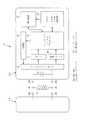
図1は、非接触ICカード1を示す斜視図であり、図2はその分解斜視図、図3はブロック図、図4は拡大断面図である。 FIG. 1 is a perspective view showing a
これらの図に示したように、非接触ICカード1は、動作周波数が異なる2つのICチップ21(21a,21b)と1つのループアンテナ22とで構成される非接触型ICタグ23が搭載された非接触型のICカードである。非接触型ICタグ23は、一般にRF−ID(Radio Frequency Identification)タグと呼ばれるものであり、電波または電磁波を用いて非接触の通信を行う機能、および情報を記憶する機能を有する。 As shown in these figures, the
非接触ICカード1は、キャッシュカード、クレジットカード、定期券、プリペイドカード、社員証、学生証などの複数の用途に利用されるもので、外形が長方形板状であり、複数の部材を積層して構成されている。 The
この非接触ICカード1は、情報記憶部として2つのICチップ21a,21bが設けられており、このICチップ21a,21bのどちらに対してループアンテナ22を接続するか切り替える切替部5が備えられている。 The
詳述すると、図2に示すように非接触ICカード1は、主にカード大の第1ラミネート部材2、カード大のスペーサ部材11、およびカード大の第2ラミネート部材15が上からこの順で重合接着されて構成されている。 Specifically, as shown in FIG. 2, the
底面にあたる第2ラミネート部材15は、接着される内側面にループアンテナ22が設けられている。このループアンテナ22は、プリント配線等によって構成された一重のループ(二重や三重といった複数重のループでもよい)であり、両端に接点24,24が設けられている。この接点24,24の互いの間は、第2ラミネート部材15の短手方向幅と比べて充分小さく構成されており、この実施形態では、ICチップ21a,21bの大きさと同程度の間隔に構成されている。また接点24,24は、第2ラミネート部材15に接着固定され、内側面(図2の上方)へ突出している。第2ラミネート部材15の外側面である裏面は、印刷等が施された化粧面である。 The
スペーサ部材11は、第2ラミネート部材15と同一サイズで肉厚一定の平面形状に形成されている。スペーサ部材11の短手方向中央には、前記接点24,24の位置を囲繞するように長方形のスライド用穴12が設けられている。このスライド用穴12における左右の長手辺は平行な一直線状のスライドガイド13,13を構成している。 The
スペーサ部材11のスライド用穴12内には、切替部5が収納される。この切替部5は、板状部材6と操作部7とICチップ21a,21bと接点20a,20bとで構成されている。 The
板状部材6は、スライド用穴12の左右幅と同一か僅かに小さい横幅で、スライド用穴12の縦幅より短い縦幅の長方形であり、肉厚一定の平面形状に形成されている。この板状部材6の両側辺8,8は、互いに平行で一直線状に形成されている。 The plate-
操作部7は、板状部材6の縦方向の一端で幅方向中央に表面側(第1ラミネート部材2側)に突出形成され、その表面は滑り止め加工がなされている。 The
ICチップ21a,21bは、板状部材6の裏面側(第2ラミネート部材15側)に、前後方向に並べて接着固定されており、該ICチップ21a,21bの端子が、それぞれ接点20a,20bに電気的に接続されている。この接点20a,20bは、板状部材6の裏面側に接着固定されており、裏面側へ突出している。接点20aと接点20bは、前後方向に一定間隔を隔てて一直線に配設されており、接点20aと接点20bの間には電気回路が存在しないように構成されている。 The
このように構成された切替部5は、スペーサ部材11のスライド用穴12内で、側辺8,8がスライドガイド13,13に沿って安定して前後方向にスライド移動できる。 The
第1ラミネート部材2は、第2ラミネート部材15と同一サイズで肉厚一定の平面形状に形成されている。第1ラミネート部材2の短手方向中央には、前記操作部7の位置を囲繞するように長方形の操作用穴3が設けられている。この操作用穴3における左右の長手辺は平行な一直線状の操作ガイド4,4を構成している。この操作用穴3内には、切替部5の操作部7が前後動可能に位置する。この操作部7の両側辺は、操作ガイド4,4でガイドされ、これにより安定して前後にスライド移動するように構成されている。第1ラミネート部材2の表面は、印刷等が施された化粧面である。 The
前記第1ラミネート部材2、板状部材6、スペーサ部材11、および第2ラミネート部材15は、紙や樹脂など通信波(電磁波や電波など)を通過許容する素材で形成すればよく、同一素材で形成する、あるいは別素材で形成することができる。 The
また、板状部材6は、適度な剛性を有する素材で構成することが好ましく、第1ラミネート部材2、スペーサ部材11、および第2ラミネート部材15は、少なくとも全てが重合して接着固定された状態で適度な剛性を有する素材で構成することが好ましい。 The plate-
また、第1ラミネート部材2、スペーサ部材11、および第2ラミネート部材15は、少なくともスライド用穴12の周囲については強固に接着固定することが好ましい。これにより、スライド用穴12の周囲の接着が剥がれて切替部5が意図しない方向へ移動することや、第1ラミネート部材2と第2ラミネート部材15の間が浮いて接点20a,20bと接点24との接触が悪くなることを防止できる。 Moreover, it is preferable that the
図3は、非接触ICカード1のブロック図を示す。
非接触ICカード1は、ICチップ21a,21bおよびループアンテナ22で構成されており、ループアンテナ22の接点24がICチップ21aの接点20aとICチップ21bの接点20bとのどちらに接続されるかによって、駆動するICチップを切り替えるように構成されている。FIG. 3 shows a block diagram of the
The
ICチップ21aは、ループアンテナ22と並列にキャパシタ41が接続されており、該キャパシタ41の後段のアナログフロントエンド42からコマンド43および伝送クロック44がコントロールマイクロプロセッサ46に入力される。 A
コントロールマイクロプロセッサ46は、前記コマンド43および伝送クロック44を受けて、ROM、RAM、およびEEPROM等で構成されるメモリ48に対してデータの読み書きを実行し、必要に応じて暗号処理47も実行する。またコントロールマイクロプロセッサ46は、変調器45にデータを送信する。 Upon receiving the
変調器45は、コントロールマイクロプロセッサ46から受信したデータをアナログ信号に変調し、アナログフロントエンド42に送る。このようにして、ICチップ21aは、第1の周波数を用いて動作する第1機能として、例えばキャッシュカード、クレジットカード、定期券、プリペイドカード、社員証、学生証などのアプリケーション機能を備えることができる。 The
ICチップ21bは、動作周波数やアプリケーション機能が異なる以外は、ICチップ21aと同一の構成であるので、その詳細な説明を省略する。このICチップ21bは、ICチップ21aと異なる第2の周波数を用いて動作する第2機能として、例えばキャッシュカード、クレジットカード、定期券、プリペイドカード、社員証、学生証などのアプリケーション機能のうちICチップ21aと異なるアプリケーション機能を備えることができる。 Since the
以上の構成により、利用者は操作部7を操作してスライド移動させるだけで、図1(A)に示したようにICチップ21aを用いて通信する第1機能実行状態と、図1(B)に示したようにICチップ21bを用いて通信する第2機能実行状態とを容易に切り替えることができる。 With the above configuration, the user simply operates the
つまり、第1機能実行状態では、図1(A)に示すように操作部7が操作用穴3の手前側に位置し、図4(A)に示すように、接点20aと接点24とが接触し、ICチップ21aとループアンテナ22とが電気的に接続される。従って、適宜の質問器からループアンテナ22が受けた磁界による誘導起電力でICチップ21aが駆動でき、またICチップ21aがループアンテナ22を通じて質問器と非接触通信することができる。このとき、接点20aと接点24とが互いに突出しているため、電気的な接続を確実に行うことができる。 That is, in the first function execution state, the
第2機能実行状態では、図1(B)に示すように操作部7が操作用穴3の奥側に位置し、図4(B)に示すように、接点20bと接点24とが接触し、ICチップ21bとループアンテナ22とが電気的に接続される。従って、適宜の質問器からループアンテナ22が受けた磁界による誘導起電力でICチップ21bが駆動でき、またICチップ21bがループアンテナ22を通じて質問器と非接触通信することができる。このとき、接点20bと接点24とが互いに突出しているため、電気的な接続を確実に行うことができる。 In the second function execution state, as shown in FIG. 1 (B), the
このように、利用者は、第1機能を実行する第1機能実行状態と、第2機能を実行する第2機能実行状態とを、操作部7を前後動させるという簡単な動作で確実に切り替えることができる。これにより、1つの非接触ICカード1を第1機能と第2機能の二つの用途で使用できる。従って、例えば第1機能としてドアの開閉機能を設定し、第2機能として鉄道の自動改札の通過機能を設定して、通常は第1機能を有効にしておき、鉄道の自動改札を通過するときに第2機能に切り替えるといった利用が可能になる。 In this way, the user reliably switches between the first function execution state for executing the first function and the second function execution state for executing the second function by a simple operation of moving the
また、非接触ICカード1は、平面状の複数の部材を重合配置して切替部5をスライド移動可能に構成しているため、薄型のカード形状に形成するのが容易であり、安価に製造することができる。 Further, the
なお、ICチップ21(21a,21b)側の接点20(20a,20b)とループアンテナ22側の接点24とをいずれも突出させて形成したが、いずれか一方のみを突出させる、あるいは両方突出させない構成としてもよい。この場合でも、接点20,24が互いに接触さえすれば電気的に接続されるため、第1機能と第2機能の切り替えを実行することができる。 The contact 20 (20a, 20b) on the IC chip 21 (21a, 21b) side and the
また、ICチップ21は2つとしたが、これに限らず複数備えて順次切り替え可能に構成してもよい。この場合、多種類の機能を1つの非接触ICカード1に持たせることができる。 In addition, the number of
また、接点24は、接点20a,20bのいずれかと接続するかを切り替える構成としたが、これに加えていずれの接点20a,20bとも接続しない非接続状態にも切替部5で切り替え可能に構成してもよい。これにより、第1機能と第2機能のいずれも使用しない状態にして非通信状態にでき、第1機能や第2機能への不正なアクセスを回避することができる。 In addition, the
図5は、実施例2の非接触ICタグ9の分解斜視図を示す。
この非接触ICタグ9は、実施例1のスライド方式によって接点20aと接点20bのいずれが接点24と接続するか切り替える構成と異なり、押下式によって切り替える構成にしたものであり、実施例1の非接触ICカード1より上下の厚みが厚く、前後左右の大きさが小さいタグ状のものである。FIG. 5 is an exploded perspective view of the
The
この非接触ICタグ9は、板状部材6の上下両面にICチップ21a,21bがそれぞれ配置され、接点20a,20bが切替部5の一端面で上下に一直線に配置されている。切替部5の底部には、第2ラミネート部材15との間に板ばね19が備えられている。この板ばね19は、切替部5を上方へ付勢する。 In the
また、切替部5は、上下面が外装部材18で覆われ、この外装部材18と板状部材6との間に充填剤17が充填されている。これにより、ICチップ21a,21bが位置ずれ等しないように構成されている。 Further, the upper and lower surfaces of the
第1ラミネート部材2および切替部5の上面には、全体を覆う表面シート16が設けられている。この表面シート16は、柔軟に変形し、かつ復元する材料で構成されている。 On the upper surfaces of the
その他の構成は、実施例1の非接触ICカード1と同一であるので、その詳細な説明を省略する。 Since other configurations are the same as those of the
以上の構成により、通常状態では図5(A)に示すように接点20bと接点24され、第2機能実行状態となる。また、切替部5を押下した場合は、接点20aと接点24が接続し、第1機能実行状態となる。このようにして、第1機能と第2機能の切り替えを容易に実行できる。 With the above configuration, in the normal state, as shown in FIG. 5A, the
なお、切替部5を押下している間のみ第1機能を実行する構成としているが、1度押下すると手を離しても押下状態を維持して第1機能実行状態を維持し、もう一度押下すると復帰して第2機能実行状態に移行する構成にしてもよい。 Note that the first function is executed only while the
図6は、実施例3の非接触ICカード1の分解斜視図を示す。
この非接触ICカード1は、表面シート31、第1非接触ICラベル32、絶縁シート33、第2非接触ICラベル34、および背面シート35が上からこの順で重合接着されて構成されている。FIG. 6 is an exploded perspective view of the
The
上面にあたる表面シート31は、適宜の剛性を有する樹脂等の素材によってカード大に形成されており、印刷等が施された化粧面により表面が構成されている。 The
第1非接触ICラベル32は、フィルムにプリント配線したループアンテナ22aと、ICチップ21aとが設けられており、ループアンテナ22aとICチップ21aは接続されている。このICチップ21aは、例えば0.8GHzの周波数帯で通信する第1機能を備えている。 The first
絶縁シート33は、炭素などの絶縁素材によってカード大に形成されているシートである。 The insulating sheet 33 is a sheet that is formed on a large card by an insulating material such as carbon.
第2非接触ICラベル34は、フィルムにプリント配線したループアンテナ22bと、ICチップ21bとが設けられている。このICチップ21bは、例えば13.56MHzの周波数帯で通信する第2機能を備えている。 The second
底面にあたる背面シート35は、適宜の剛性を有する樹脂等の素材によってカード大に形成されており、外側面である裏面に、磁気ストライプ36を備えている。この裏面の磁気ストライプ36以外の部分は、印刷等が施された化粧面である。 The
以上の構成により、1つの非接触ICカード1に複数の機能を持たせることができる。つまり、複数の非接触ICラベル(32,34)を備えることで、第1機能と第2機能のそれぞれをいつでも実行することができる。第1非接触ICラベル32と第2非接触ICラベル34は、絶縁シート33で分離されているため、互いのループアンテナ22a,22bが干渉し合うことを防止できる。 With the above configuration, one
なお、以上の各実施形態では、非接触ICカード1で説明したが、カード型のものに限らず、携帯電話機に備えた非接触IC媒体や、紙タイプやシールタイプの非接触ICタグに備えられた非接触IC媒体により構成してもよい。この場合でも、同一の作用効果を奏することができる。 In the above embodiments, the
図7は、実施例4の非接触ICカード1の分解斜視図を示し、図8は、実施例4の非接触ICカード1の部分拡大断面図を示す。
この非接触ICカード1は、表面シート31、第1非接触ICラベル32、セパレータ50、第2非接触ICラベル34、および背面シート35が上からこの順で重合接着されて構成されている。FIG. 7 shows an exploded perspective view of the
The
上面にあたる表面シート31は、適宜の剛性を有する樹脂等の素材によってカード大(カードサイズ)に形成されており、印刷等が施された化粧面により表面が構成されている。 The
第1非接触ICラベル32は、フィルムにプリント配線したループアンテナ22aと、ICチップ21aとが互いに接続されて設けられている。このICチップ21aは、ICチップ21bと同一の周波数帯でICチップ21bよりも強い電磁波を受けて通信するように構成されている。このICチップ21aは、例えば13.56MHzの周波数帯でリーダライタと30cm程度はなれた位置から非接触通信できる構成とされており、例えば鉄道の乗車券として利用できる第1機能を備えている。ICチップ21aの構成は、図3と共に説明した実施例1のICチップ21aと同一であるので、その詳細な説明を省略する。 The first
セパレータ50は、炭素などの絶縁素材によってカード大に形成されているシートである。
このセパレータ50は、中間層として設けられたカード大の電磁波遮断層52と、該電磁波遮断層52よりも第1非接触ICラベル32側に重合配置されたカード大の第1電磁波吸収層51と、該電磁波遮断層52よりも第2非接触ICラベル34側に重合配置されたカード大の第2電磁波吸収層53とで構成されている。The
The
ここで、電磁波遮断層52は、アルミ又は銅などの電磁波遮断材料で構成されている。
第1電磁波吸収層51は、軟磁性体など電磁波を分散、吸収する材料で構成されている。この実施例では、第2電磁波吸収層53よりも電磁波吸収能力を強めるべく、パーマロイを用いて構成されている。Here, the electromagnetic
The first electromagnetic
第2電磁波吸収層53は、軟磁性体など電磁波を分散、吸収する材料で構成されている。この実施例では、第1電磁波吸収層51よりも電磁波吸収能力を弱めるべく、金属磁性体フレークを樹脂に充填して形成されている。肉厚は、0.5mm〜0.25mm程度の厚みが好ましく、この実施形態では0.25mm程度に形成されている。またこの第2電磁波吸収層53は、推奨周波数帯域を100MHz〜3GHz程度とし、初透磁率(at 10MHz)が21〜32程度となるように形成されている。この第2電磁波吸収層53の素材には、第1電磁波吸収層51よりも電磁波吸収能力を弱めるべく、フェライト等を用いることが好ましい。 The second electromagnetic
第2非接触ICラベル34は、フィルムにプリント配線したループアンテナ22bと、ICチップ21bとが互いに接続されて設けられている。このICチップ21bは、ICチップ21aと同一の周波数帯でICチップ21aよりも弱い電磁波を受けて通信するように構成されている。このICチップ21bは、例えば13.56MHzの周波数帯でリーダライタと10cm程度はなれた位置(ICチップ21aの場合よりも短い距離)から非接触通信できる通信できる構成とされており、たとえばキャッシングに用いることとができる第2機能を備えている。ICチップ21bの構成は、図3と共に説明した実施例1のICチップ21bと同一であるので、その詳細な説明を省略する。 The second
底面にあたる背面シート35は、適宜の剛性を有する樹脂等の素材によってカード大に形成されており、外側面である裏面に、磁気ストライプ36を備えている。この裏面の磁気ストライプ36以外の部分は、印刷等が施された化粧面である。 The
以上の構成により、1つの非接触ICカード1に複数の機能を持たせることができる。つまり、複数の非接触ICラベル(32,34)を備えることで、第1機能と第2機能のそれぞれをいつでも実行することができる。第1非接触ICラベル32と第2非接触ICラベル34は、セパレータ50で分離されているため、互いのループアンテナ22a,22bが干渉し合うことを防止できる。 With the above configuration, one
また、セパレータ50に設けられた第1電磁波吸収層51と第2電磁波吸収層53との電磁波吸収性能を異ならせているため、第1非接触ICラベル32と第2非接触ICラベル34の各通信を確実に実行させることができる。 Further, since the electromagnetic wave absorption performance of the first electromagnetic
詳述すると、例えば第2電磁波吸収層53を第1電磁波吸収層51と同一の電磁波吸収性能を有するように構成すると、第1非接触ICラベル32は強い磁界で良好に通信できるが、第2非接触ICラベル34と弱い磁界で通信しようとしても第2電磁波吸収層53の電磁波吸収性能が強すぎて通信できなくなることがある。また、逆に第1電磁波吸収層51を第2電磁波吸収層53と同一の電磁波吸収性能を有するように構成すると、第2非接触ICラベル34は弱い磁界で良好に通信できるが、第1非接触ICラベル32と強い磁界で通信しようとすると第2非接触ICラベル34までもが反応して電磁波が混線することがある。このような問題を、第1電磁波吸収層51と第2電磁波吸収層53との電磁波吸収性能を異ならせることで解決することができる。 More specifically, for example, if the second electromagnetic
また、通信に強い電磁波を用いる第1非接触ICラベル32側の第1電磁波吸収層51の材質を第2電磁波吸収層53の材質よりも電磁波吸収性能が高いものにしたため、全体を肉薄に構成することができる。
つまり、仮に同一の材質を用いて第1電磁波吸収層51と第2電磁波吸収層53とを作成する場合、第1電磁波吸収層51の電磁波吸収性能を高めるために第1電磁波吸収層51を第2電磁波吸収層53より肉厚に形成する必要が生じ、非接触ICカード1の全体の肉厚が厚くなってしまう。しかし、この実施例4のように異なる材料とすることで、全体の肉厚を薄くすることができる。In addition, since the material of the first electromagnetic
That is, if the first electromagnetic
なお、第1電磁波吸収層51や第2電磁波吸収層53の材質は、パーマロイやフェライトに限らず、酸化鉄、クロム、ニッケル、アモルファス合金、電磁鋼、珪素鉄、Fe−AL合金、センダスト合金、カルボニル鉄、またはこれらの複数の材料の混合材料で構成してもよい。 The material of the first electromagnetic
この発明の構成と、上述の実施形態との対応において、
この発明の非接触IC媒体は、非接触ICカード1に対応し、
以下同様に、
切替手段は、実施形態の切替部5に対応し、
接点は、接点20a,20bに対応し、
ICチップは、ICチップ21a,21bに対応し、
アンテナは、ループアンテナ22,22a,22bに対応し、
共用アンテナは、ループアンテナ22に対応し、
個別のアンテナは、ループアンテナ22a,22bにするも、
この発明は、上述の実施形態の構成のみに限定されるものではなく、多くの実施の形態を得ることができる。In correspondence between the configuration of the present invention and the above-described embodiment,
The non-contact IC medium of the present invention corresponds to the
Similarly,
The switching means corresponds to the
The contacts correspond to the
The IC chip corresponds to the
The antenna corresponds to the
The shared antenna corresponds to the
Individual antennas are
The present invention is not limited only to the configuration of the above-described embodiment, and many embodiments can be obtained.
5…切替部
20a,20b…接点
21a,21b…ICチップ
22,22a,22b…ループアンテナ
23…非接触型ICタグ
50…セパレータ
51…第1電磁波吸収層
52…電磁波遮断層
53…第2電磁波吸収層DESCRIPTION OF
Claims (7)
Translated fromJapanese前記ICチップを複数搭載した
非接触IC媒体。A non-contact IC medium comprising an antenna that performs non-contact communication and an IC chip that performs a control operation,
A non-contact IC medium on which a plurality of the IC chips are mounted.
第2のICチップと第2のアンテナとで構成され前記第1非接触ICシートよりも強い電磁波を受けて駆動する第2非接触ICシートと、
前記第1非接触ICシートと前記第2非接触ICシートとの間に挟まれるセパレータとを備え、
該セパレータを、
電磁波を遮断する電磁波遮断層と、
該電磁波遮断層よりも前記第1非接触ICシート側に重合配置される第1電磁波吸収層と、
前記電磁波遮断層よりも前記第2非接触ICシート側に重合配置される第2電磁波吸収層とで構成し、
該第2電磁波吸収層の電磁波吸収能力を、前記第1電磁波吸収層よりも高く構成した
非接触IC媒体。A first non-contact IC sheet composed of a first IC chip and a first antenna;
A second non-contact IC sheet configured by a second IC chip and a second antenna and driven by receiving an electromagnetic wave stronger than the first non-contact IC sheet;
A separator sandwiched between the first non-contact IC sheet and the second non-contact IC sheet,
The separator,
An electromagnetic wave blocking layer for blocking electromagnetic waves,
A first electromagnetic wave absorbing layer that is polymerized and disposed closer to the first non-contact IC sheet than the electromagnetic wave blocking layer;
The second electromagnetic wave absorbing layer is arranged on the second non-contact IC sheet side than the electromagnetic wave blocking layer,
The non-contact IC medium which comprised the electromagnetic wave absorption capability of this 2nd electromagnetic wave absorption layer higher than the said 1st electromagnetic wave absorption layer.
請求項2記載の非接触IC媒体。The non-contact IC medium according to claim 2, wherein a material of the second electromagnetic wave absorbing layer is made of a material having an electromagnetic wave absorbing ability higher than that of the first electromagnetic wave absorbing layer.
請求項2または3記載の非接触IC媒体。The non-contact IC medium according to claim 2 or 3, wherein a relationship between an operating frequency of the first IC chip and an operating frequency of the second IC chip is the same frequency or an integral multiple of the frequency.
請求項1記載の非接触IC媒体。The non-contact IC medium according to claim 1, wherein the antenna is a shared antenna shared by a plurality of the IC chips.
前記アンテナと接続するICチップの接点を切り替える切替手段を備えた
請求項5記載の非接触IC媒体。Provided with a contact for connection to the plurality of IC chips,
6. The non-contact IC medium according to claim 5, further comprising switching means for switching contact points of the IC chip connected to the antenna.
請求項5または6記載の非接触IC媒体。7. The non-contact IC medium according to claim 5, wherein ones having different operating frequencies are used for the plurality of IC chips.
Priority Applications (2)
| Application Number | Priority Date | Filing Date | Title |
|---|---|---|---|
| JP2007001246AJP2007287128A (en) | 2006-03-22 | 2007-01-09 | Non-contact ic medium |
| PCT/JP2007/074900WO2008084689A1 (en) | 2007-01-09 | 2007-12-26 | Noncontact ic medium |
Applications Claiming Priority (2)
| Application Number | Priority Date | Filing Date | Title |
|---|---|---|---|
| JP2006078717 | 2006-03-22 | ||
| JP2007001246AJP2007287128A (en) | 2006-03-22 | 2007-01-09 | Non-contact ic medium |
Publications (1)
| Publication Number | Publication Date |
|---|---|
| JP2007287128Atrue JP2007287128A (en) | 2007-11-01 |
Family
ID=38758805
Family Applications (1)
| Application Number | Title | Priority Date | Filing Date |
|---|---|---|---|
| JP2007001246AWithdrawnJP2007287128A (en) | 2006-03-22 | 2007-01-09 | Non-contact ic medium |
Country Status (1)
| Country | Link |
|---|---|
| JP (1) | JP2007287128A (en) |
Cited By (70)
| Publication number | Priority date | Publication date | Assignee | Title |
|---|---|---|---|---|
| JP4671001B2 (en)* | 2008-07-04 | 2011-04-13 | 株式会社村田製作所 | Wireless IC device |
| US7967216B2 (en) | 2008-05-22 | 2011-06-28 | Murata Manufacturing Co., Ltd. | Wireless IC device |
| US8177138B2 (en) | 2008-10-29 | 2012-05-15 | Murata Manufacturing Co., Ltd. | Radio IC device |
| US8191791B2 (en) | 2007-07-17 | 2012-06-05 | Murata Manufacturing Co., Ltd. | Wireless IC device and electronic apparatus |
| US8228765B2 (en) | 2006-06-30 | 2012-07-24 | Murata Manufacturing Co., Ltd. | Optical disc |
| US8299929B2 (en) | 2006-09-26 | 2012-10-30 | Murata Manufacturing Co., Ltd. | Inductively coupled module and item with inductively coupled module |
| US8336786B2 (en) | 2010-03-12 | 2012-12-25 | Murata Manufacturing Co., Ltd. | Wireless communication device and metal article |
| US8342416B2 (en) | 2009-01-09 | 2013-01-01 | Murata Manufacturing Co., Ltd. | Wireless IC device, wireless IC module and method of manufacturing wireless IC module |
| US8360330B2 (en) | 2007-12-26 | 2013-01-29 | Murata Manufacturing Co., Ltd. | Antenna device and radio frequency IC device |
| US8381997B2 (en) | 2009-06-03 | 2013-02-26 | Murata Manufacturing Co., Ltd. | Radio frequency IC device and method of manufacturing the same |
| US8400365B2 (en) | 2009-11-20 | 2013-03-19 | Murata Manufacturing Co., Ltd. | Antenna device and mobile communication terminal |
| US8418928B2 (en) | 2009-04-14 | 2013-04-16 | Murata Manufacturing Co., Ltd. | Wireless IC device component and wireless IC device |
| US8424762B2 (en) | 2007-04-14 | 2013-04-23 | Murata Manufacturing Co., Ltd. | Wireless IC device and component for wireless IC device |
| US8424769B2 (en) | 2010-07-08 | 2013-04-23 | Murata Manufacturing Co., Ltd. | Antenna and RFID device |
| US8531346B2 (en) | 2007-04-26 | 2013-09-10 | Murata Manufacturing Co., Ltd. | Wireless IC device |
| US8546927B2 (en) | 2010-09-03 | 2013-10-01 | Murata Manufacturing Co., Ltd. | RFIC chip mounting structure |
| US8552870B2 (en) | 2007-07-09 | 2013-10-08 | Murata Manufacturing Co., Ltd. | Wireless IC device |
| US8583043B2 (en) | 2009-01-16 | 2013-11-12 | Murata Manufacturing Co., Ltd. | High-frequency device and wireless IC device |
| US8590797B2 (en) | 2008-05-21 | 2013-11-26 | Murata Manufacturing Co., Ltd. | Wireless IC device |
| US8596545B2 (en) | 2008-05-28 | 2013-12-03 | Murata Manufacturing Co., Ltd. | Component of wireless IC device and wireless IC device |
| US8602310B2 (en) | 2010-03-03 | 2013-12-10 | Murata Manufacturing Co., Ltd. | Radio communication device and radio communication terminal |
| US8610636B2 (en) | 2007-12-20 | 2013-12-17 | Murata Manufacturing Co., Ltd. | Radio frequency IC device |
| US8613395B2 (en) | 2011-02-28 | 2013-12-24 | Murata Manufacturing Co., Ltd. | Wireless communication device |
| US8676117B2 (en) | 2006-01-19 | 2014-03-18 | Murata Manufacturing Co., Ltd. | Wireless IC device and component for wireless IC device |
| US8680971B2 (en) | 2009-09-28 | 2014-03-25 | Murata Manufacturing Co., Ltd. | Wireless IC device and method of detecting environmental state using the device |
| US8692718B2 (en) | 2008-11-17 | 2014-04-08 | Murata Manufacturing Co., Ltd. | Antenna and wireless IC device |
| US8718727B2 (en) | 2009-12-24 | 2014-05-06 | Murata Manufacturing Co., Ltd. | Antenna having structure for multi-angled reception and mobile terminal including the antenna |
| US8720789B2 (en) | 2012-01-30 | 2014-05-13 | Murata Manufacturing Co., Ltd. | Wireless IC device |
| US8740093B2 (en) | 2011-04-13 | 2014-06-03 | Murata Manufacturing Co., Ltd. | Radio IC device and radio communication terminal |
| US8757500B2 (en) | 2007-05-11 | 2014-06-24 | Murata Manufacturing Co., Ltd. | Wireless IC device |
| US8770489B2 (en) | 2011-07-15 | 2014-07-08 | Murata Manufacturing Co., Ltd. | Radio communication device |
| US8797148B2 (en) | 2008-03-03 | 2014-08-05 | Murata Manufacturing Co., Ltd. | Radio frequency IC device and radio communication system |
| US8797225B2 (en) | 2011-03-08 | 2014-08-05 | Murata Manufacturing Co., Ltd. | Antenna device and communication terminal apparatus |
| US8810456B2 (en) | 2009-06-19 | 2014-08-19 | Murata Manufacturing Co., Ltd. | Wireless IC device and coupling method for power feeding circuit and radiation plate |
| US8814056B2 (en) | 2011-07-19 | 2014-08-26 | Murata Manufacturing Co., Ltd. | Antenna device, RFID tag, and communication terminal apparatus |
| US8847831B2 (en) | 2009-07-03 | 2014-09-30 | Murata Manufacturing Co., Ltd. | Antenna and antenna module |
| US8853549B2 (en) | 2009-09-30 | 2014-10-07 | Murata Manufacturing Co., Ltd. | Circuit substrate and method of manufacturing same |
| US8870077B2 (en) | 2008-08-19 | 2014-10-28 | Murata Manufacturing Co., Ltd. | Wireless IC device and method for manufacturing same |
| US8878739B2 (en) | 2011-07-14 | 2014-11-04 | Murata Manufacturing Co., Ltd. | Wireless communication device |
| US8905316B2 (en) | 2010-05-14 | 2014-12-09 | Murata Manufacturing Co., Ltd. | Wireless IC device |
| US8905296B2 (en) | 2011-12-01 | 2014-12-09 | Murata Manufacturing Co., Ltd. | Wireless integrated circuit device and method of manufacturing the same |
| US8937576B2 (en) | 2011-04-05 | 2015-01-20 | Murata Manufacturing Co., Ltd. | Wireless communication device |
| US8944335B2 (en) | 2010-09-30 | 2015-02-03 | Murata Manufacturing Co., Ltd. | Wireless IC device |
| US8976075B2 (en) | 2009-04-21 | 2015-03-10 | Murata Manufacturing Co., Ltd. | Antenna device and method of setting resonant frequency of antenna device |
| US8981906B2 (en) | 2010-08-10 | 2015-03-17 | Murata Manufacturing Co., Ltd. | Printed wiring board and wireless communication system |
| US8991713B2 (en) | 2011-01-14 | 2015-03-31 | Murata Manufacturing Co., Ltd. | RFID chip package and RFID tag |
| US9024725B2 (en) | 2009-11-04 | 2015-05-05 | Murata Manufacturing Co., Ltd. | Communication terminal and information processing system |
| US9024837B2 (en) | 2010-03-31 | 2015-05-05 | Murata Manufacturing Co., Ltd. | Antenna and wireless communication device |
| US9104950B2 (en) | 2009-01-30 | 2015-08-11 | Murata Manufacturing Co., Ltd. | Antenna and wireless IC device |
| US9117157B2 (en) | 2009-10-02 | 2015-08-25 | Murata Manufacturing Co., Ltd. | Wireless IC device and electromagnetic coupling module |
| US9123996B2 (en) | 2010-05-14 | 2015-09-01 | Murata Manufacturing Co., Ltd. | Wireless IC device |
| US9165239B2 (en) | 2006-04-26 | 2015-10-20 | Murata Manufacturing Co., Ltd. | Electromagnetic-coupling-module-attached article |
| US9166291B2 (en) | 2010-10-12 | 2015-10-20 | Murata Manufacturing Co., Ltd. | Antenna device and communication terminal apparatus |
| US9178279B2 (en) | 2009-11-04 | 2015-11-03 | Murata Manufacturing Co., Ltd. | Wireless IC tag, reader-writer, and information processing system |
| US9231305B2 (en) | 2008-10-24 | 2016-01-05 | Murata Manufacturing Co., Ltd. | Wireless IC device |
| US9236651B2 (en) | 2010-10-21 | 2016-01-12 | Murata Manufacturing Co., Ltd. | Communication terminal device |
| US9281873B2 (en) | 2008-05-26 | 2016-03-08 | Murata Manufacturing Co., Ltd. | Wireless IC device system and method of determining authenticity of wireless IC device |
| US9378452B2 (en) | 2011-05-16 | 2016-06-28 | Murata Manufacturing Co., Ltd. | Radio IC device |
| US9444143B2 (en) | 2009-10-16 | 2016-09-13 | Murata Manufacturing Co., Ltd. | Antenna and wireless IC device |
| US9461363B2 (en) | 2009-11-04 | 2016-10-04 | Murata Manufacturing Co., Ltd. | Communication terminal and information processing system |
| US9460320B2 (en) | 2009-10-27 | 2016-10-04 | Murata Manufacturing Co., Ltd. | Transceiver and radio frequency identification tag reader |
| US9460376B2 (en) | 2007-07-18 | 2016-10-04 | Murata Manufacturing Co., Ltd. | Radio IC device |
| US9543642B2 (en) | 2011-09-09 | 2017-01-10 | Murata Manufacturing Co., Ltd. | Antenna device and wireless device |
| US9558384B2 (en) | 2010-07-28 | 2017-01-31 | Murata Manufacturing Co., Ltd. | Antenna apparatus and communication terminal instrument |
| US9692128B2 (en) | 2012-02-24 | 2017-06-27 | Murata Manufacturing Co., Ltd. | Antenna device and wireless communication device |
| US9727765B2 (en) | 2010-03-24 | 2017-08-08 | Murata Manufacturing Co., Ltd. | RFID system including a reader/writer and RFID tag |
| US9761923B2 (en) | 2011-01-05 | 2017-09-12 | Murata Manufacturing Co., Ltd. | Wireless communication device |
| US10013650B2 (en) | 2010-03-03 | 2018-07-03 | Murata Manufacturing Co., Ltd. | Wireless communication module and wireless communication device |
| JP2018190279A (en)* | 2017-05-10 | 2018-11-29 | 大日本印刷株式会社 | Non-contact IC card |
| US10235544B2 (en) | 2012-04-13 | 2019-03-19 | Murata Manufacturing Co., Ltd. | Inspection method and inspection device for RFID tag |
- 2007
- 2007-01-09JPJP2007001246Apatent/JP2007287128A/ennot_activeWithdrawn
Cited By (88)
| Publication number | Priority date | Publication date | Assignee | Title |
|---|---|---|---|---|
| US8676117B2 (en) | 2006-01-19 | 2014-03-18 | Murata Manufacturing Co., Ltd. | Wireless IC device and component for wireless IC device |
| US8725071B2 (en) | 2006-01-19 | 2014-05-13 | Murata Manufacturing Co., Ltd. | Wireless IC device and component for wireless IC device |
| US9165239B2 (en) | 2006-04-26 | 2015-10-20 | Murata Manufacturing Co., Ltd. | Electromagnetic-coupling-module-attached article |
| US8228765B2 (en) | 2006-06-30 | 2012-07-24 | Murata Manufacturing Co., Ltd. | Optical disc |
| US8299929B2 (en) | 2006-09-26 | 2012-10-30 | Murata Manufacturing Co., Ltd. | Inductively coupled module and item with inductively coupled module |
| US8424762B2 (en) | 2007-04-14 | 2013-04-23 | Murata Manufacturing Co., Ltd. | Wireless IC device and component for wireless IC device |
| US8531346B2 (en) | 2007-04-26 | 2013-09-10 | Murata Manufacturing Co., Ltd. | Wireless IC device |
| US8757500B2 (en) | 2007-05-11 | 2014-06-24 | Murata Manufacturing Co., Ltd. | Wireless IC device |
| US8662403B2 (en) | 2007-07-04 | 2014-03-04 | Murata Manufacturing Co., Ltd. | Wireless IC device and component for wireless IC device |
| US8552870B2 (en) | 2007-07-09 | 2013-10-08 | Murata Manufacturing Co., Ltd. | Wireless IC device |
| US8191791B2 (en) | 2007-07-17 | 2012-06-05 | Murata Manufacturing Co., Ltd. | Wireless IC device and electronic apparatus |
| US8413907B2 (en) | 2007-07-17 | 2013-04-09 | Murata Manufacturing Co., Ltd. | Wireless IC device and electronic apparatus |
| US9830552B2 (en) | 2007-07-18 | 2017-11-28 | Murata Manufacturing Co., Ltd. | Radio IC device |
| US9460376B2 (en) | 2007-07-18 | 2016-10-04 | Murata Manufacturing Co., Ltd. | Radio IC device |
| US8610636B2 (en) | 2007-12-20 | 2013-12-17 | Murata Manufacturing Co., Ltd. | Radio frequency IC device |
| US8915448B2 (en) | 2007-12-26 | 2014-12-23 | Murata Manufacturing Co., Ltd. | Antenna device and radio frequency IC device |
| US8360330B2 (en) | 2007-12-26 | 2013-01-29 | Murata Manufacturing Co., Ltd. | Antenna device and radio frequency IC device |
| US8797148B2 (en) | 2008-03-03 | 2014-08-05 | Murata Manufacturing Co., Ltd. | Radio frequency IC device and radio communication system |
| US8973841B2 (en) | 2008-05-21 | 2015-03-10 | Murata Manufacturing Co., Ltd. | Wireless IC device |
| US9022295B2 (en) | 2008-05-21 | 2015-05-05 | Murata Manufacturing Co., Ltd. | Wireless IC device |
| US8590797B2 (en) | 2008-05-21 | 2013-11-26 | Murata Manufacturing Co., Ltd. | Wireless IC device |
| US7967216B2 (en) | 2008-05-22 | 2011-06-28 | Murata Manufacturing Co., Ltd. | Wireless IC device |
| US9281873B2 (en) | 2008-05-26 | 2016-03-08 | Murata Manufacturing Co., Ltd. | Wireless IC device system and method of determining authenticity of wireless IC device |
| US8596545B2 (en) | 2008-05-28 | 2013-12-03 | Murata Manufacturing Co., Ltd. | Component of wireless IC device and wireless IC device |
| JP4671001B2 (en)* | 2008-07-04 | 2011-04-13 | 株式会社村田製作所 | Wireless IC device |
| US9077067B2 (en) | 2008-07-04 | 2015-07-07 | Murata Manufacturing Co., Ltd. | Radio IC device |
| US8870077B2 (en) | 2008-08-19 | 2014-10-28 | Murata Manufacturing Co., Ltd. | Wireless IC device and method for manufacturing same |
| US9231305B2 (en) | 2008-10-24 | 2016-01-05 | Murata Manufacturing Co., Ltd. | Wireless IC device |
| US8177138B2 (en) | 2008-10-29 | 2012-05-15 | Murata Manufacturing Co., Ltd. | Radio IC device |
| US8692718B2 (en) | 2008-11-17 | 2014-04-08 | Murata Manufacturing Co., Ltd. | Antenna and wireless IC device |
| US8917211B2 (en) | 2008-11-17 | 2014-12-23 | Murata Manufacturing Co., Ltd. | Antenna and wireless IC device |
| US8342416B2 (en) | 2009-01-09 | 2013-01-01 | Murata Manufacturing Co., Ltd. | Wireless IC device, wireless IC module and method of manufacturing wireless IC module |
| US8544759B2 (en) | 2009-01-09 | 2013-10-01 | Murata Manufacturing., Ltd. | Wireless IC device, wireless IC module and method of manufacturing wireless IC module |
| US8583043B2 (en) | 2009-01-16 | 2013-11-12 | Murata Manufacturing Co., Ltd. | High-frequency device and wireless IC device |
| US9104950B2 (en) | 2009-01-30 | 2015-08-11 | Murata Manufacturing Co., Ltd. | Antenna and wireless IC device |
| US8690070B2 (en) | 2009-04-14 | 2014-04-08 | Murata Manufacturing Co., Ltd. | Wireless IC device component and wireless IC device |
| US8418928B2 (en) | 2009-04-14 | 2013-04-16 | Murata Manufacturing Co., Ltd. | Wireless IC device component and wireless IC device |
| US8876010B2 (en) | 2009-04-14 | 2014-11-04 | Murata Manufacturing Co., Ltd | Wireless IC device component and wireless IC device |
| US8976075B2 (en) | 2009-04-21 | 2015-03-10 | Murata Manufacturing Co., Ltd. | Antenna device and method of setting resonant frequency of antenna device |
| US9203157B2 (en) | 2009-04-21 | 2015-12-01 | Murata Manufacturing Co., Ltd. | Antenna device and method of setting resonant frequency of antenna device |
| US9564678B2 (en) | 2009-04-21 | 2017-02-07 | Murata Manufacturing Co., Ltd. | Antenna device and method of setting resonant frequency of antenna device |
| US8381997B2 (en) | 2009-06-03 | 2013-02-26 | Murata Manufacturing Co., Ltd. | Radio frequency IC device and method of manufacturing the same |
| US8810456B2 (en) | 2009-06-19 | 2014-08-19 | Murata Manufacturing Co., Ltd. | Wireless IC device and coupling method for power feeding circuit and radiation plate |
| US8847831B2 (en) | 2009-07-03 | 2014-09-30 | Murata Manufacturing Co., Ltd. | Antenna and antenna module |
| US8680971B2 (en) | 2009-09-28 | 2014-03-25 | Murata Manufacturing Co., Ltd. | Wireless IC device and method of detecting environmental state using the device |
| US8853549B2 (en) | 2009-09-30 | 2014-10-07 | Murata Manufacturing Co., Ltd. | Circuit substrate and method of manufacturing same |
| US9117157B2 (en) | 2009-10-02 | 2015-08-25 | Murata Manufacturing Co., Ltd. | Wireless IC device and electromagnetic coupling module |
| US9444143B2 (en) | 2009-10-16 | 2016-09-13 | Murata Manufacturing Co., Ltd. | Antenna and wireless IC device |
| US9460320B2 (en) | 2009-10-27 | 2016-10-04 | Murata Manufacturing Co., Ltd. | Transceiver and radio frequency identification tag reader |
| US9024725B2 (en) | 2009-11-04 | 2015-05-05 | Murata Manufacturing Co., Ltd. | Communication terminal and information processing system |
| US9178279B2 (en) | 2009-11-04 | 2015-11-03 | Murata Manufacturing Co., Ltd. | Wireless IC tag, reader-writer, and information processing system |
| US9461363B2 (en) | 2009-11-04 | 2016-10-04 | Murata Manufacturing Co., Ltd. | Communication terminal and information processing system |
| US8704716B2 (en) | 2009-11-20 | 2014-04-22 | Murata Manufacturing Co., Ltd. | Antenna device and mobile communication terminal |
| US8400365B2 (en) | 2009-11-20 | 2013-03-19 | Murata Manufacturing Co., Ltd. | Antenna device and mobile communication terminal |
| US8718727B2 (en) | 2009-12-24 | 2014-05-06 | Murata Manufacturing Co., Ltd. | Antenna having structure for multi-angled reception and mobile terminal including the antenna |
| US8602310B2 (en) | 2010-03-03 | 2013-12-10 | Murata Manufacturing Co., Ltd. | Radio communication device and radio communication terminal |
| US10013650B2 (en) | 2010-03-03 | 2018-07-03 | Murata Manufacturing Co., Ltd. | Wireless communication module and wireless communication device |
| US8336786B2 (en) | 2010-03-12 | 2012-12-25 | Murata Manufacturing Co., Ltd. | Wireless communication device and metal article |
| US8528829B2 (en) | 2010-03-12 | 2013-09-10 | Murata Manufacturing Co., Ltd. | Wireless communication device and metal article |
| US9727765B2 (en) | 2010-03-24 | 2017-08-08 | Murata Manufacturing Co., Ltd. | RFID system including a reader/writer and RFID tag |
| US9024837B2 (en) | 2010-03-31 | 2015-05-05 | Murata Manufacturing Co., Ltd. | Antenna and wireless communication device |
| US9123996B2 (en) | 2010-05-14 | 2015-09-01 | Murata Manufacturing Co., Ltd. | Wireless IC device |
| US8905316B2 (en) | 2010-05-14 | 2014-12-09 | Murata Manufacturing Co., Ltd. | Wireless IC device |
| US8424769B2 (en) | 2010-07-08 | 2013-04-23 | Murata Manufacturing Co., Ltd. | Antenna and RFID device |
| US9558384B2 (en) | 2010-07-28 | 2017-01-31 | Murata Manufacturing Co., Ltd. | Antenna apparatus and communication terminal instrument |
| US8981906B2 (en) | 2010-08-10 | 2015-03-17 | Murata Manufacturing Co., Ltd. | Printed wiring board and wireless communication system |
| US8546927B2 (en) | 2010-09-03 | 2013-10-01 | Murata Manufacturing Co., Ltd. | RFIC chip mounting structure |
| US8944335B2 (en) | 2010-09-30 | 2015-02-03 | Murata Manufacturing Co., Ltd. | Wireless IC device |
| US9166291B2 (en) | 2010-10-12 | 2015-10-20 | Murata Manufacturing Co., Ltd. | Antenna device and communication terminal apparatus |
| US9236651B2 (en) | 2010-10-21 | 2016-01-12 | Murata Manufacturing Co., Ltd. | Communication terminal device |
| US9761923B2 (en) | 2011-01-05 | 2017-09-12 | Murata Manufacturing Co., Ltd. | Wireless communication device |
| US8991713B2 (en) | 2011-01-14 | 2015-03-31 | Murata Manufacturing Co., Ltd. | RFID chip package and RFID tag |
| US8613395B2 (en) | 2011-02-28 | 2013-12-24 | Murata Manufacturing Co., Ltd. | Wireless communication device |
| US8757502B2 (en) | 2011-02-28 | 2014-06-24 | Murata Manufacturing Co., Ltd. | Wireless communication device |
| US8960561B2 (en) | 2011-02-28 | 2015-02-24 | Murata Manufacturing Co., Ltd. | Wireless communication device |
| US8797225B2 (en) | 2011-03-08 | 2014-08-05 | Murata Manufacturing Co., Ltd. | Antenna device and communication terminal apparatus |
| US8937576B2 (en) | 2011-04-05 | 2015-01-20 | Murata Manufacturing Co., Ltd. | Wireless communication device |
| US8740093B2 (en) | 2011-04-13 | 2014-06-03 | Murata Manufacturing Co., Ltd. | Radio IC device and radio communication terminal |
| US9378452B2 (en) | 2011-05-16 | 2016-06-28 | Murata Manufacturing Co., Ltd. | Radio IC device |
| US8878739B2 (en) | 2011-07-14 | 2014-11-04 | Murata Manufacturing Co., Ltd. | Wireless communication device |
| US8770489B2 (en) | 2011-07-15 | 2014-07-08 | Murata Manufacturing Co., Ltd. | Radio communication device |
| US8814056B2 (en) | 2011-07-19 | 2014-08-26 | Murata Manufacturing Co., Ltd. | Antenna device, RFID tag, and communication terminal apparatus |
| US9543642B2 (en) | 2011-09-09 | 2017-01-10 | Murata Manufacturing Co., Ltd. | Antenna device and wireless device |
| US8905296B2 (en) | 2011-12-01 | 2014-12-09 | Murata Manufacturing Co., Ltd. | Wireless integrated circuit device and method of manufacturing the same |
| US8720789B2 (en) | 2012-01-30 | 2014-05-13 | Murata Manufacturing Co., Ltd. | Wireless IC device |
| US9692128B2 (en) | 2012-02-24 | 2017-06-27 | Murata Manufacturing Co., Ltd. | Antenna device and wireless communication device |
| US10235544B2 (en) | 2012-04-13 | 2019-03-19 | Murata Manufacturing Co., Ltd. | Inspection method and inspection device for RFID tag |
| JP2018190279A (en)* | 2017-05-10 | 2018-11-29 | 大日本印刷株式会社 | Non-contact IC card |
Similar Documents
| Publication | Publication Date | Title |
|---|---|---|
| JP2007287128A (en) | Non-contact ic medium | |
| US20210081748A1 (en) | Proximity and dual interface metal cards and methods of making card bodies with two metal layers | |
| CA2684625C (en) | Anti-interrogation for portable device | |
| US7533826B2 (en) | Electronic wallet | |
| US6367701B1 (en) | Portable data transmission device, and fixing element | |
| CA2714412C (en) | Non-contact ic card communication controller and non-contact ic card holder | |
| WO2008022031A2 (en) | Proximity payment card with user-actuated switch and methods of making the card | |
| WO2007088898A1 (en) | Noncontact ic medium, noncontact ic card, electronic device, electronic device cover, and noncontact ic medium reader/writer | |
| WO2006075359A1 (en) | Ic tag storing case | |
| KR102275151B1 (en) | Non-contacting metal card having a sheet for absorbing electromagnetic wave | |
| US20120256727A1 (en) | Selectively enabled rfid tag | |
| JP4256466B1 (en) | Non-contact IC card communication adjustment plate and non-contact IC card holder | |
| JP5040371B2 (en) | Non-contact data carrier device | |
| JP6347437B1 (en) | Non-contact near field communication card and data parallel processing system using the same | |
| KR20100033571A (en) | Smart card capable of controlling rf function | |
| EP4264489B1 (en) | Assembly for shielding at least one radio-frequency chip and method for making the same | |
| JP2005327208A (en) | Shield body and non-contact IC card storage case | |
| WO2019123985A1 (en) | Noncontact near-field communication card and data parallel processing system using same | |
| JP4714201B2 (en) | card case | |
| JP2004220305A (en) | Composite IC card | |
| JP2006216083A (en) | Non-contact identification tag, external device, and security system using them | |
| JP2006091964A (en) | Double-sided non-contact IC sheet | |
| US20120256004A1 (en) | Selectively enabled rfid tag | |
| JP2006167011A (en) | Portable card housing device | |
| JP2003132329A (en) | Non-contact IC card |
Legal Events
| Date | Code | Title | Description |
|---|---|---|---|
| RD04 | Notification of resignation of power of attorney | Free format text:JAPANESE INTERMEDIATE CODE: A7424 Effective date:20090917 | |
| A521 | Written amendment | Free format text:JAPANESE INTERMEDIATE CODE: A523 Effective date:20091008 | |
| A300 | Withdrawal of application because of no request for examination | Free format text:JAPANESE INTERMEDIATE CODE: A300 Effective date:20100406 |