JP2007286150A - Electro-optical device, current control TFT substrate, and manufacturing method thereof - Google Patents
Electro-optical device, current control TFT substrate, and manufacturing method thereofDownload PDFInfo
- Publication number
- JP2007286150A JP2007286150AJP2006110543AJP2006110543AJP2007286150AJP 2007286150 AJP2007286150 AJP 2007286150AJP 2006110543 AJP2006110543 AJP 2006110543AJP 2006110543 AJP2006110543 AJP 2006110543AJP 2007286150 AJP2007286150 AJP 2007286150A
- Authority
- JP
- Japan
- Prior art keywords
- line
- electrode
- transistor
- resist
- drain
- Prior art date
- Legal status (The legal status is an assumption and is not a legal conclusion. Google has not performed a legal analysis and makes no representation as to the accuracy of the status listed.)
- Pending
Links
Images


Classifications
- G—PHYSICS
- G09—EDUCATION; CRYPTOGRAPHY; DISPLAY; ADVERTISING; SEALS
- G09G—ARRANGEMENTS OR CIRCUITS FOR CONTROL OF INDICATING DEVICES USING STATIC MEANS TO PRESENT VARIABLE INFORMATION
- G09G3/00—Control arrangements or circuits, of interest only in connection with visual indicators other than cathode-ray tubes
- G09G3/20—Control arrangements or circuits, of interest only in connection with visual indicators other than cathode-ray tubes for presentation of an assembly of a number of characters, e.g. a page, by composing the assembly by combination of individual elements arranged in a matrix no fixed position being assigned to or needed to be assigned to the individual characters or partial characters
- G09G3/22—Control arrangements or circuits, of interest only in connection with visual indicators other than cathode-ray tubes for presentation of an assembly of a number of characters, e.g. a page, by composing the assembly by combination of individual elements arranged in a matrix no fixed position being assigned to or needed to be assigned to the individual characters or partial characters using controlled light sources
- G09G3/30—Control arrangements or circuits, of interest only in connection with visual indicators other than cathode-ray tubes for presentation of an assembly of a number of characters, e.g. a page, by composing the assembly by combination of individual elements arranged in a matrix no fixed position being assigned to or needed to be assigned to the individual characters or partial characters using controlled light sources using electroluminescent panels
- G09G3/32—Control arrangements or circuits, of interest only in connection with visual indicators other than cathode-ray tubes for presentation of an assembly of a number of characters, e.g. a page, by composing the assembly by combination of individual elements arranged in a matrix no fixed position being assigned to or needed to be assigned to the individual characters or partial characters using controlled light sources using electroluminescent panels semiconductive, e.g. using light-emitting diodes [LED]
- G09G3/3208—Control arrangements or circuits, of interest only in connection with visual indicators other than cathode-ray tubes for presentation of an assembly of a number of characters, e.g. a page, by composing the assembly by combination of individual elements arranged in a matrix no fixed position being assigned to or needed to be assigned to the individual characters or partial characters using controlled light sources using electroluminescent panels semiconductive, e.g. using light-emitting diodes [LED] organic, e.g. using organic light-emitting diodes [OLED]
- G09G3/3225—Control arrangements or circuits, of interest only in connection with visual indicators other than cathode-ray tubes for presentation of an assembly of a number of characters, e.g. a page, by composing the assembly by combination of individual elements arranged in a matrix no fixed position being assigned to or needed to be assigned to the individual characters or partial characters using controlled light sources using electroluminescent panels semiconductive, e.g. using light-emitting diodes [LED] organic, e.g. using organic light-emitting diodes [OLED] using an active matrix
- G09G3/3233—Control arrangements or circuits, of interest only in connection with visual indicators other than cathode-ray tubes for presentation of an assembly of a number of characters, e.g. a page, by composing the assembly by combination of individual elements arranged in a matrix no fixed position being assigned to or needed to be assigned to the individual characters or partial characters using controlled light sources using electroluminescent panels semiconductive, e.g. using light-emitting diodes [LED] organic, e.g. using organic light-emitting diodes [OLED] using an active matrix with pixel circuitry controlling the current through the light-emitting element
- H—ELECTRICITY
- H10—SEMICONDUCTOR DEVICES; ELECTRIC SOLID-STATE DEVICES NOT OTHERWISE PROVIDED FOR
- H10D—INORGANIC ELECTRIC SEMICONDUCTOR DEVICES
- H10D30/00—Field-effect transistors [FET]
- H10D30/60—Insulated-gate field-effect transistors [IGFET]
- H10D30/67—Thin-film transistors [TFT]
- H10D30/674—Thin-film transistors [TFT] characterised by the active materials
- H10D30/6755—Oxide semiconductors, e.g. zinc oxide, copper aluminium oxide or cadmium stannate
- H—ELECTRICITY
- H10—SEMICONDUCTOR DEVICES; ELECTRIC SOLID-STATE DEVICES NOT OTHERWISE PROVIDED FOR
- H10D—INORGANIC ELECTRIC SEMICONDUCTOR DEVICES
- H10D64/00—Electrodes of devices having potential barriers
- H10D64/60—Electrodes characterised by their materials
- H10D64/62—Electrodes ohmically coupled to a semiconductor
- H—ELECTRICITY
- H10—SEMICONDUCTOR DEVICES; ELECTRIC SOLID-STATE DEVICES NOT OTHERWISE PROVIDED FOR
- H10D—INORGANIC ELECTRIC SEMICONDUCTOR DEVICES
- H10D86/00—Integrated devices formed in or on insulating or conducting substrates, e.g. formed in silicon-on-insulator [SOI] substrates or on stainless steel or glass substrates
- H10D86/01—Manufacture or treatment
- H10D86/021—Manufacture or treatment of multiple TFTs
- H10D86/0231—Manufacture or treatment of multiple TFTs using masks, e.g. half-tone masks
- H—ELECTRICITY
- H10—SEMICONDUCTOR DEVICES; ELECTRIC SOLID-STATE DEVICES NOT OTHERWISE PROVIDED FOR
- H10D—INORGANIC ELECTRIC SEMICONDUCTOR DEVICES
- H10D86/00—Integrated devices formed in or on insulating or conducting substrates, e.g. formed in silicon-on-insulator [SOI] substrates or on stainless steel or glass substrates
- H10D86/40—Integrated devices formed in or on insulating or conducting substrates, e.g. formed in silicon-on-insulator [SOI] substrates or on stainless steel or glass substrates characterised by multiple TFTs
- H10D86/421—Integrated devices formed in or on insulating or conducting substrates, e.g. formed in silicon-on-insulator [SOI] substrates or on stainless steel or glass substrates characterised by multiple TFTs having a particular composition, shape or crystalline structure of the active layer
- H10D86/423—Integrated devices formed in or on insulating or conducting substrates, e.g. formed in silicon-on-insulator [SOI] substrates or on stainless steel or glass substrates characterised by multiple TFTs having a particular composition, shape or crystalline structure of the active layer comprising semiconductor materials not belonging to the Group IV, e.g. InGaZnO
- H—ELECTRICITY
- H10—SEMICONDUCTOR DEVICES; ELECTRIC SOLID-STATE DEVICES NOT OTHERWISE PROVIDED FOR
- H10D—INORGANIC ELECTRIC SEMICONDUCTOR DEVICES
- H10D86/00—Integrated devices formed in or on insulating or conducting substrates, e.g. formed in silicon-on-insulator [SOI] substrates or on stainless steel or glass substrates
- H10D86/40—Integrated devices formed in or on insulating or conducting substrates, e.g. formed in silicon-on-insulator [SOI] substrates or on stainless steel or glass substrates characterised by multiple TFTs
- H10D86/441—Interconnections, e.g. scanning lines
- H—ELECTRICITY
- H10—SEMICONDUCTOR DEVICES; ELECTRIC SOLID-STATE DEVICES NOT OTHERWISE PROVIDED FOR
- H10D—INORGANIC ELECTRIC SEMICONDUCTOR DEVICES
- H10D86/00—Integrated devices formed in or on insulating or conducting substrates, e.g. formed in silicon-on-insulator [SOI] substrates or on stainless steel or glass substrates
- H10D86/40—Integrated devices formed in or on insulating or conducting substrates, e.g. formed in silicon-on-insulator [SOI] substrates or on stainless steel or glass substrates characterised by multiple TFTs
- H10D86/481—Integrated devices formed in or on insulating or conducting substrates, e.g. formed in silicon-on-insulator [SOI] substrates or on stainless steel or glass substrates characterised by multiple TFTs integrated with passive devices, e.g. auxiliary capacitors
- H—ELECTRICITY
- H10—SEMICONDUCTOR DEVICES; ELECTRIC SOLID-STATE DEVICES NOT OTHERWISE PROVIDED FOR
- H10D—INORGANIC ELECTRIC SEMICONDUCTOR DEVICES
- H10D86/00—Integrated devices formed in or on insulating or conducting substrates, e.g. formed in silicon-on-insulator [SOI] substrates or on stainless steel or glass substrates
- H10D86/40—Integrated devices formed in or on insulating or conducting substrates, e.g. formed in silicon-on-insulator [SOI] substrates or on stainless steel or glass substrates characterised by multiple TFTs
- H10D86/60—Integrated devices formed in or on insulating or conducting substrates, e.g. formed in silicon-on-insulator [SOI] substrates or on stainless steel or glass substrates characterised by multiple TFTs wherein the TFTs are in active matrices
- H—ELECTRICITY
- H10—SEMICONDUCTOR DEVICES; ELECTRIC SOLID-STATE DEVICES NOT OTHERWISE PROVIDED FOR
- H10K—ORGANIC ELECTRIC SOLID-STATE DEVICES
- H10K59/00—Integrated devices, or assemblies of multiple devices, comprising at least one organic light-emitting element covered by group H10K50/00
- H10K59/10—OLED displays
- H10K59/12—Active-matrix OLED [AMOLED] displays
- H10K59/131—Interconnections, e.g. wiring lines or terminals
- G—PHYSICS
- G09—EDUCATION; CRYPTOGRAPHY; DISPLAY; ADVERTISING; SEALS
- G09G—ARRANGEMENTS OR CIRCUITS FOR CONTROL OF INDICATING DEVICES USING STATIC MEANS TO PRESENT VARIABLE INFORMATION
- G09G2300/00—Aspects of the constitution of display devices
- G09G2300/04—Structural and physical details of display devices
- G09G2300/0404—Matrix technologies
- G09G2300/0417—Special arrangements specific to the use of low carrier mobility technology
- G—PHYSICS
- G09—EDUCATION; CRYPTOGRAPHY; DISPLAY; ADVERTISING; SEALS
- G09G—ARRANGEMENTS OR CIRCUITS FOR CONTROL OF INDICATING DEVICES USING STATIC MEANS TO PRESENT VARIABLE INFORMATION
- G09G2300/00—Aspects of the constitution of display devices
- G09G2300/08—Active matrix structure, i.e. with use of active elements, inclusive of non-linear two terminal elements, in the pixels together with light emitting or modulating elements
- G09G2300/0809—Several active elements per pixel in active matrix panels
- G09G2300/0842—Several active elements per pixel in active matrix panels forming a memory circuit, e.g. a dynamic memory with one capacitor
- G09G2300/0852—Several active elements per pixel in active matrix panels forming a memory circuit, e.g. a dynamic memory with one capacitor being a dynamic memory with more than one capacitor
- G—PHYSICS
- G09—EDUCATION; CRYPTOGRAPHY; DISPLAY; ADVERTISING; SEALS
- G09G—ARRANGEMENTS OR CIRCUITS FOR CONTROL OF INDICATING DEVICES USING STATIC MEANS TO PRESENT VARIABLE INFORMATION
- G09G2320/00—Control of display operating conditions
- G09G2320/02—Improving the quality of display appearance
- G09G2320/029—Improving the quality of display appearance by monitoring one or more pixels in the display panel, e.g. by monitoring a fixed reference pixel
- G09G2320/0295—Improving the quality of display appearance by monitoring one or more pixels in the display panel, e.g. by monitoring a fixed reference pixel by monitoring each display pixel
- G—PHYSICS
- G09—EDUCATION; CRYPTOGRAPHY; DISPLAY; ADVERTISING; SEALS
- G09G—ARRANGEMENTS OR CIRCUITS FOR CONTROL OF INDICATING DEVICES USING STATIC MEANS TO PRESENT VARIABLE INFORMATION
- G09G2320/00—Control of display operating conditions
- G09G2320/04—Maintaining the quality of display appearance
- G09G2320/043—Preventing or counteracting the effects of ageing
Landscapes
- Engineering & Computer Science (AREA)
- Physics & Mathematics (AREA)
- Computer Hardware Design (AREA)
- General Physics & Mathematics (AREA)
- Theoretical Computer Science (AREA)
- Microelectronics & Electronic Packaging (AREA)
- Electroluminescent Light Sources (AREA)
- Control Of El Displays (AREA)
- Control Of Indicators Other Than Cathode Ray Tubes (AREA)
- Devices For Indicating Variable Information By Combining Individual Elements (AREA)
- Thin Film Transistor (AREA)
Abstract
Translated fromJapaneseDescription
Translated fromJapanese本発明は、電気光学装置、並びに、電流制御用TFT基板及びその製造方法に関し、特に、直接的に交流電流を制御し、高周波の交流電流を出力することができ、また、安定して大電力を出力することができ、さらに、製造原価のコストダウンを図ることの可能な電気光学装置、並びに、電流制御用TFT基板及びその製造方法に関する。 The present invention relates to an electro-optical device, a current control TFT substrate, and a manufacturing method thereof, and in particular, can directly control an alternating current and output a high-frequency alternating current, and can stably generate a large power. In addition, the present invention relates to an electro-optical device that can reduce the manufacturing cost, a current control TFT substrate, and a manufacturing method thereof.
有機EL表示装置は、LCD(Liquid Crystal Display)表示装置に代わる次世代の表示装置や固体照明として注目されている。その理由は、有機EL(Electronic Luminescence)素子が、自発光素子であるために視野角依存性が少なく、また、バックライトや反射光が不要であるために低消費電力であるなどといった優れた特性を有しているからである。
また、有機EL表示装置の駆動方式として、単純マトリクス駆動方式とアクティブマトリクス駆動方式があり、アクティブマトリクス駆動方式の方が、画質や応答速度などの点で単純マトリクス駆動方式より優れている。アクティブマトリクス駆動方式の有機EL表示装置は、各画素にスイッチングトランジスタや駆動トランジスタなどの形成されたTFT(薄膜トランジスタ)基板(一般的に、電流制御用TFT基板とも呼称される。)を有しており、各有機EL素子に流れる電流量を制御している。Organic EL display devices have attracted attention as next-generation display devices and solid-state lighting that replace LCD (Liquid Crystal Display) display devices. The reason for this is that the organic EL (Electronic Luminescence) element is a self-luminous element and therefore has a small viewing angle dependency, and also has excellent characteristics such as low power consumption because no backlight or reflected light is required. It is because it has.
There are a simple matrix driving method and an active matrix driving method as driving methods of the organic EL display device, and the active matrix driving method is superior to the simple matrix driving method in terms of image quality and response speed. An active matrix driving type organic EL display device has a TFT (thin film transistor) substrate (generally also referred to as a current control TFT substrate) in which a switching transistor and a driving transistor are formed in each pixel. The amount of current flowing through each organic EL element is controlled.
ところで、上記アクティブマトリクス駆動方式の有機EL表示装置は、優れた特性を有しているものの、駆動トランジスタの特性のばらつきのために、各画素において有機EL素子に流れる電流量が異なり、輝度むらが発生することがあった。また、有機EL素子は、電流発光装置であり、電流の大小により発光強度を変化させることができるものの、連続発光させた場合、時間の経過とともに発光強度が低下していた。
このような短所を解決するために、様々な駆動回路を有する有機EL表示装置が提案されてきた。By the way, although the above active matrix driving type organic EL display device has excellent characteristics, the amount of current flowing through the organic EL element differs in each pixel due to variation in characteristics of driving transistors, resulting in uneven luminance. It sometimes occurred. In addition, the organic EL element is a current light emitting device, and the light emission intensity can be changed depending on the magnitude of the current. However, when the light is continuously emitted, the light emission intensity is decreased with time.
In order to solve such disadvantages, organic EL display devices having various drive circuits have been proposed.
(従来例)
たとえば、特許文献1には、光学的フィードバックを可能とするアドレス可能画像表示画素の技術が開示されている。このアドレス可能画像表示画素は、光センサとフィードバック読み出し回路が基板上に形成されている。光センサは、基板上に形成され、発光体の発する光に反応してフィードバック電圧信号を生成するために発光体の発する光を検出するように発光体と光学的に結合しており、また、フィードバック読み出し回路は、フィードバック電圧信号に反応して発光体の光出力を示すフィードバック信号を出力し、トランジスタ増幅器、読み出し回路をリセットする手段、及び、選択スイッチを備えている。(Conventional example)
For example,
また、特許文献2には、アクティブマトリクス構成において、各画素に電流測定素子を設けずに有機EL素子に流れる電流を測定し、TFT特性のばらつきによる輝度むらを補正する電気光学装置の技術が開示されている。この電気光学装置は、アクティブ素子と有機EL素子がマトリクス状に配置され、有機EL素子に電流を供給する複数の電流供給線が配置され、各電流供給線に電流測定素子が設けられており、一本の走査線に走査電圧を与え、それと同期して各データ線に所定のデータ電圧を供給し、電流測定素子により有機EL素子に流れる電流値を測定する。次に、同一の走査線に走査電圧を与え、それと同期して各データ線に電気光学素子を0階調にするデータ信号を供給する。この駆動動作を各走査線に対して行い、得られた電流測定値にもとづいて各アクティブ素子に与えるデータ電圧を補正することを特徴としている。
また、特許文献3には、駆動トランジスタの特性のばらつきを補償するための補償トランジスタを各画素に設けた電気光学装置の技術が開示されている。この電気光学装置は、各画素の駆動トランジスタと補償トランジスタがカレント・ミラー回路を構成しており、各画素の駆動トランジスタと補償トランジスタの利得係数を一致させることにより、各画素に形成されている駆動トランジスタにばらつきが発生しても、各画素の被駆動素子に同じ大きさの電流を供給することができ、駆動トランジスタの特性ばらつきに起因する輝度むらを抑えることができる。
しかしながら、上記特許文献1、3に記載された技術は、各画素の構成要素が増大し、構造が複雑化するために歩留まりが低下するといった問題や、製造原価のコストダウンを図ることができないといった問題があった。
また、特許文献3に記載された技術は、製造段階において、各画素の駆動トランジスタと補償トランジスタの利得係数を一致させ、駆動トランジスタの特性のばらつきに起因する輝度むらを抑えることができるものの、使用されると、各画素の駆動トランジスタと補償トランジスタの通電される時間が異なり、劣化による性能の差が、輝度むらとして現れるといった問題があった。
さらに、上記特許文献2に記載された技術は、多数(n個)の有機EL素子に電流を供給する一本の電流供給線に電流測定素子を接続してあり、同一列の各画素に対して、一つの画素の有機EL素子に流れる電流を測定できるものの、測定中は、同一列の他の画素に電流を流さないようにする必要がある(同一列の多数の画素に電流を流しながらでは、一つの画素の有機EL素子に流れる電流変動分を測定できない。)。すなわち、同一列の他の画素に電流を流さない状態で測定する必要があり、測定条件が制限されるといった問題があった。However, the techniques described in
Further, although the technique described in
Furthermore, in the technique described in
また、一般的な有機EL表示装置は、複数のシリコン半導体を用いた薄膜トランジスタの配設された電流制御用TFT基板を有しているが、電流を大量に流した場合、シリコン半導体それ自体が劣化し、有機EL発光素子に印加する電圧や電流を制御できなくなる場合があるといった問題があった。さらに、直流電流を大量に流すことにより、有機EL発光装置の寿命が短くなるといった問題があった。
また、電気光学素子として無機EL素子を用いた電気光学装置は、交流電源により無機EL素子を駆動させているが、一回の駆動中に交流駆動を行うことはできず、次ぎの駆動においては、電圧を反転させてから無機EL素子を駆動させている。すなわち、見かけ上、交流駆動となっているものの、一回のスキャン中は直流駆動であり、交流駆動の周波数を上げるには、スキャンの周波数をも上げる必要があり、高周波数化を図れないといった問題があった。Further, a general organic EL display device has a current control TFT substrate in which thin film transistors using a plurality of silicon semiconductors are arranged. However, when a large amount of current is passed, the silicon semiconductor itself deteriorates. However, there is a problem that the voltage and current applied to the organic EL light emitting element may not be controlled. Furthermore, there is a problem that the life of the organic EL light emitting device is shortened by flowing a large amount of direct current.
In addition, an electro-optical device using an inorganic EL element as an electro-optical element drives the inorganic EL element by an AC power source, but cannot perform AC driving during one driving, and in the next driving The inorganic EL element is driven after the voltage is inverted. In other words, although it is apparently AC drive, it is DC drive during one scan, and to increase the frequency of AC drive, it is necessary to increase the scan frequency, and it is not possible to increase the frequency. There was a problem.
本発明は、係る課題に鑑みなされたものであり、直接的に交流電流を制御し、高周波の交流電流を出力することができ、また、安定して大電力を出力することができ、さらに、製造原価のコストダウンを図ることの可能な電気光学装置、並びに、電流制御用TFT基板及びその製造方法の提供を目的とする。 The present invention has been made in view of such problems, and can directly control alternating current, output high-frequency alternating current, stably output large power, and It is an object of the present invention to provide an electro-optical device capable of reducing the manufacturing cost, a current control TFT substrate, and a manufacturing method thereof.
上記目的を達成するために、本発明の電流制御用TFT基板は、電気光学素子に電流を供給する駆動トランジスタと、この駆動トランジスタを制御するスイッチングトランジスタが形成された電流制御用TFT基板であって、前記駆動トランジスタの活性層が、酸化物半導体層からなる構成としてある。
このようにすると、大きな交流電流や、大電力を投入した場合であっても、駆動トランジスタの活性層にアモルファスSiやポリSi半導体を用いたものと比べると、その性能劣化が小さく、安定性に優れるとともに、耐久性を向上させることができる。また、有機EL素子を有する発光装置に用いられた場合、発光装置の寿命を大きく延ばすことができる。In order to achieve the above object, a current control TFT substrate of the present invention is a current control TFT substrate in which a drive transistor for supplying current to an electro-optic element and a switching transistor for controlling the drive transistor are formed. The active layer of the drive transistor is composed of an oxide semiconductor layer.
In this way, even when a large alternating current or a large amount of power is applied, the performance degradation is small and stable compared to the case where amorphous Si or poly-Si semiconductor is used for the active layer of the driving transistor. While being excellent, durability can be improved. In addition, when used in a light emitting device having an organic EL element, the lifetime of the light emitting device can be greatly extended.
また、好ましくは、前記スイッチングトランジスタの活性層を、酸化物半導体層とするとよい。
このようにすると、スイッチングトランジスタの活性層にアモルファスSiやポリSi半導体を用いたものと比べると、耐久性を向上させることができる。Preferably, the active layer of the switching transistor is an oxide semiconductor layer.
In this case, the durability can be improved as compared with the case where amorphous silicon or poly silicon semiconductor is used for the active layer of the switching transistor.
また、好ましくは、前記駆動トランジスタが、ソース線、ドレイン線、ソース電極又はドレイン電極のうち少なくとも一つ以上を備え、前記ソース線、ドレイン線、ソース電極又はドレイン電極のうち少なくとも一つ以上が、酸化物導電体層からなり、かつ、該酸化物導電体層が、前記電気光学素子の画素電極を兼ねるとよい。
このようにすると、製造する際に使用するマスク数を削減でき、製造工程が削減されることにより、生産効率が向上し製造原価のコストダウンを図ることができる。また、通常、酸化物導電体層が、ソース線,ドレイン線,ソース電極,ドレイン電極及び画素電極を兼ねる構造とされ、このようにすると、ソース線,ドレイン線,ソース電極,ドレイン電極及び画素電極を効率よく製造することができる。
なお、「酸化物導電体層が、少なくとも画素電極を兼ねる」とは、形成された酸化物導電体層が、少なくとも画素電極としての機能を有することをいう。Preferably, the driving transistor includes at least one of a source line, a drain line, a source electrode, and a drain electrode, and at least one of the source line, the drain line, the source electrode, and the drain electrode is It is preferable that the oxide conductor layer is composed of an oxide conductor layer, and the oxide conductor layer also serves as a pixel electrode of the electro-optic element.
If it does in this way, the number of masks used at the time of manufacturing can be reduced, and a manufacturing process can be reduced, thereby improving production efficiency and reducing the cost of manufacturing. In general, the oxide conductor layer has a structure also serving as a source line, a drain line, a source electrode, a drain electrode, and a pixel electrode. In this case, the source line, the drain line, the source electrode, the drain electrode, and the pixel electrode Can be manufactured efficiently.
Note that “the oxide conductor layer also serves as at least the pixel electrode” means that the formed oxide conductor layer has at least a function as a pixel electrode.
また、好ましくは、前記スイッチングトランジスタが、ソース線、ドレイン線、ソース電極又はドレイン電極のうち少なくとも一つ以上を備え、前記ソース線、ドレイン線、ソース電極又はドレイン電極のうち少なくとも一つ以上を、酸化物導電体層とするとよい。 Preferably, the switching transistor includes at least one of a source line, a drain line, a source electrode and a drain electrode, and at least one of the source line, the drain line, the source electrode and the drain electrode, An oxide conductor layer is preferable.
また、好ましくは、前記電流制御用TFT基板が、ゲート線、ソース線、ドレイン線、ゲート電極、ソース電極、ドレイン電極又は画素電極のうち少なくとも一つ以上を備え、前記ゲート線、ソース線、ドレイン線、ゲート電極、ソース電極、ドレイン電極又は画素電極のうち少なくとも一つ以上の上方に、補助導電体層を形成するとよい。
このようにすると、各配線や電極の電気抵抗を低減することができ、信頼性を向上させることができるとともに、エネルギー効率の低下を抑制することができる。Preferably, the current control TFT substrate includes at least one of a gate line, a source line, a drain line, a gate electrode, a source electrode, a drain electrode, and a pixel electrode, and the gate line, the source line, and the drain An auxiliary conductor layer may be formed above at least one of a line, a gate electrode, a source electrode, a drain electrode, and a pixel electrode.
If it does in this way, the electrical resistance of each wiring and an electrode can be reduced, reliability can be improved, and the fall of energy efficiency can be controlled.
また、上記目的を達成するために、本発明の電気光学装置は、電流により駆動される電気光学素子と、この電気光学素子に電流を供給する駆動トランジスタ及びこの駆動トランジスタを制御するスイッチングトランジスタが少なくとも形成された電流制御用TFT基板を備えた電気光学装置であって、前記電流制御用TFT基板を、上記請求項1〜5のいずれかに記載された電流制御用TFT基板とした構成としてある。
このようにすると、大きな交流電流や、大電力を投入した場合であっても、駆動トランジスタの活性層にアモルファスSiやポリSi半導体を用いたものと比べると、その性能劣化が小さく、安定性に優れるとともに、電流制御用TFT基板の耐久性を向上させることができる。したがって、電気光学装置の寿命を大きく延ばすことができる。In order to achieve the above object, the electro-optical device of the present invention includes at least an electro-optical element driven by a current, a driving transistor that supplies current to the electro-optical element, and a switching transistor that controls the driving transistor. An electro-optical device including the formed current control TFT substrate, wherein the current control TFT substrate is the current control TFT substrate according to any one of
In this way, even when a large alternating current or a large amount of power is applied, the performance degradation is small and stable compared to the case where amorphous Si or poly-Si semiconductor is used for the active layer of the drive transistor. In addition to being excellent, the durability of the current control TFT substrate can be improved. Therefore, the life of the electro-optical device can be greatly extended.
また、本発明の電気光学装置は、電流により駆動される電気光学素子と、この電気光学素子に電流を供給する駆動トランジスタと、この駆動トランジスタを制御するスイッチングトランジスタと、前記駆動トランジスタのゲート電極にキャパシタ電圧を印加するためのキャパシタと、前記電気光学素子に供給される電流を測定するための測定用トランジスタを備えた電気光学装置であって、前記スイッチングトランジスタのゲート線が、前記スイッチングトランジスタを制御するための走査線と接続され、該スイッチングトランジスタのソース線が、前記電気光学素子へ供給される電流を制御するためのデータ線と接続され、該スイッチングトランジスタのドレイン線が、前記駆動トランジスタのゲート線及び前記キャパシタの第一電極と並列に接続され、前記駆動トランジスタのソース線が、前記電気光学素子へ電流を供給するための駆動線と接続され、該駆動トランジスタのドレイン線が、前記電気光学素子、前記キャパシタの第二電極及び前記測定用トランジスタのソース線と並列に接続され、前記測定用トランジスタのゲート線が、前記走査線と接続され、該測定用トランジスタのドレイン線が、前記電気光学素子へ供給される電流を測定するための測定線と接続された構成としてある。 The electro-optical device of the present invention includes an electro-optical element driven by current, a driving transistor that supplies current to the electro-optical element, a switching transistor that controls the driving transistor, and a gate electrode of the driving transistor. An electro-optical device comprising a capacitor for applying a capacitor voltage and a measuring transistor for measuring a current supplied to the electro-optical element, wherein a gate line of the switching transistor controls the switching transistor Connected to a scanning line, a source line of the switching transistor is connected to a data line for controlling a current supplied to the electro-optic element, and a drain line of the switching transistor is connected to a gate of the driving transistor Parallel to the wire and the first electrode of the capacitor A source line of the driving transistor is connected to a driving line for supplying a current to the electro-optical element, and a drain line of the driving transistor is connected to the electro-optical element, the second electrode of the capacitor, and the For measuring the current supplied to the electro-optic element, connected in parallel to the source line of the measuring transistor, the gate line of the measuring transistor connected to the scanning line, and the drain line of the measuring transistor The measurement line is connected to the measurement line.
このようにすると、走査線に直流電圧を印加すると、スイッチングトランジスタ及び測定用トランジスタがon状態となり、データ線より供給される直流電圧・電流により、スイッチングトランジスタを介して駆動トランジスタのon状態を制御する。また、駆動線より駆動トランジスタ及び測定用トランジスタを通り、測定線ソースに流れる直流電流を測定できる。したがって、測定線を介して、電気光学素子に供給される直流電流が、所望の電流値になるまでデータ線の電圧・電流を制御することができ、電気光学素子の輝度を微調整することができる。
さらに、キャパシタの第一電極は、スイッチングトランジスタのドレイン線及び駆動トランジスタのゲート線と並列に接続されており、さらに、キャパシタの第二電極は、駆動トランジスタのドレイン線、電気光学素子及び測定用トランジスタのソース線と並列に接続されており、電気光学素子に供給される直流電流が、所望の電流値になったところで、走査線の電圧を切り、スイッチングトランジスタ及び測定用トランジスタをoff状態にしても、キャパシタに蓄えられた電圧により、駆動トランジスタ3はon状態が維持され、かつ、測定用トランジスタを通して計測された直流電流が、駆動トランジスタを介して、駆動線から電気光学素子ソースに供給され、直流駆動型の電気光学素子の安定した発光が可能となる。In this way, when a DC voltage is applied to the scanning line, the switching transistor and the measurement transistor are turned on, and the on state of the drive transistor is controlled via the switching transistor by the DC voltage / current supplied from the data line. . Further, it is possible to measure a direct current flowing from the drive line to the measurement line source through the drive transistor and the measurement transistor. Therefore, the voltage and current of the data line can be controlled until the direct current supplied to the electro-optical element through the measurement line reaches a desired current value, and the brightness of the electro-optical element can be finely adjusted. it can.
Further, the first electrode of the capacitor is connected in parallel with the drain line of the switching transistor and the gate line of the driving transistor, and the second electrode of the capacitor is the drain line of the driving transistor, the electro-optic element, and the measuring transistor. When the direct current supplied to the electro-optic element reaches a desired current value, the scanning line voltage is turned off and the switching transistor and the measurement transistor are turned off. The driving
また、好ましくは、前記電気光学素子を、直流電流駆動型の電気光学素子とするとよい。
このようにすると、直流電流駆動型の電気光学素子の安定した発光が可能となる。Preferably, the electro-optical element is a direct current drive type electro-optical element.
By doing so, it is possible to emit light stably by the direct current drive type electro-optical element.
また、好ましくは、前記直流電流駆動型の電気光学素子を、有機EL素子及び/又は直流駆動型無機EL素子とするとよい。
このようにすると、有機EL素子及び/又は直流駆動型無機EL素子の安定した発光が可能となる。Preferably, the direct current drive type electro-optical element is an organic EL element and / or a direct current drive type inorganic EL element.
In this way, the organic EL element and / or the direct current drive type inorganic EL element can emit light stably.
また、本発明の電気光学装置は、電流により駆動される電気光学素子と、この電気光学素子に電流を供給する駆動トランジスタと、この駆動トランジスタを制御するスイッチングトランジスタと、前記駆動トランジスタのゲート電極にキャパシタ電圧を印加するためのキャパシタと、前記電気光学素子に供給される電流を測定するための測定用トランジスタを備えた電気光学装置であって、前記スイッチングトランジスタのゲート線が、前記スイッチングトランジスタを制御するための走査線と接続され、該スイッチングトランジスタのソース線が、前記電気光学素子へ供給される電流を制御するためのデータ線と接続され、該スイッチングトランジスタのドレイン線が、前記駆動トランジスタのゲート線及び前記キャパシタの第一電極と並列に接続され、前記駆動トランジスタのソース線が、前記電気光学素子へ電流を供給するための駆動線と接続され、該駆動トランジスタのドレイン線が、前記電気光学素子及び前記測定用トランジスタのソース線と並列に接続され、前記キャパシタの第二電極が、蓄えられた電荷を開放するためのキャパシタ線と接続され、前記測定用トランジスタのゲート線が、前記走査線と接続され、該測定用トランジスタのドレイン線が、前記電気光学素子へ供給される電流を測定するための測定線と接続された構成としてある。 The electro-optical device of the present invention includes an electro-optical element driven by current, a driving transistor that supplies current to the electro-optical element, a switching transistor that controls the driving transistor, and a gate electrode of the driving transistor. An electro-optical device comprising a capacitor for applying a capacitor voltage and a measuring transistor for measuring a current supplied to the electro-optical element, wherein a gate line of the switching transistor controls the switching transistor Connected to a scanning line, a source line of the switching transistor is connected to a data line for controlling a current supplied to the electro-optic element, and a drain line of the switching transistor is connected to a gate of the driving transistor Parallel to the wire and the first electrode of the capacitor And the source line of the driving transistor is connected to a driving line for supplying current to the electro-optical element, and the drain line of the driving transistor is connected to the source line of the electro-optical element and the measuring transistor. Connected in parallel, the second electrode of the capacitor is connected to a capacitor line for releasing the stored charge, the gate line of the measuring transistor is connected to the scanning line, and the drain of the measuring transistor is connected The line is connected to a measurement line for measuring a current supplied to the electro-optical element.
このようにすると、走査線に直流電圧を印加すると、スイッチングトランジスタ及び測定用トランジスタがon状態となり、データ線より供給される直流電圧・電流により、スイッチングトランジスタを介して駆動トランジスタのon状態を制御する。また、駆動線より駆動トランジスタ及び測定用トランジスタを通り、測定線ソースに流れる直流電流又は交流電流を測定できる。したがって、測定線を介して、電気光学素子に供給される直流電流又は交流電流が、所望の電流値になるまでデータ線の直流電圧・電流を制御することができ、電気光学素子の輝度を微調整することができる。
さらに、キャパシタの第一電極は、スイッチングトランジスタのドレイン線及び駆動トランジスタのゲート線と並列に接続されており、さらに、キャパシタの第二電極は、陰極に接地されたキャパシタ線と接続されており、電気光学素子に供給される直流電流又は交流電流が、所望の電流値になったところで、走査線の電圧を切り、スイッチングトランジスタ及び測定用トランジスタをoff状態にしても、キャパシタに蓄えられた電圧により、駆動トランジスタ3はon状態が維持され、かつ、測定用トランジスタを通して計測された直流電流又は交流電流が、駆動トランジスタを介して、駆動線から電気光学素子ソースに供給され、直流駆動型又は交流駆動型の電気光学素子の安定した発光が可能となる。In this way, when a DC voltage is applied to the scanning line, the switching transistor and the measurement transistor are turned on, and the on state of the drive transistor is controlled via the switching transistor by the DC voltage / current supplied from the data line. . Further, it is possible to measure a direct current or an alternating current flowing from the drive line to the measurement line source through the drive transistor and the measurement transistor. Therefore, the DC voltage / current of the data line can be controlled until the DC current or AC current supplied to the electro-optical element via the measurement line reaches a desired current value, and the brightness of the electro-optical element is reduced. Can be adjusted.
Furthermore, the first electrode of the capacitor is connected in parallel with the drain line of the switching transistor and the gate line of the driving transistor, and the second electrode of the capacitor is connected with the capacitor line grounded to the cathode, When the direct current or alternating current supplied to the electro-optical element reaches a desired current value, the voltage stored in the capacitor is changed even if the scanning line voltage is turned off and the switching transistor and the measurement transistor are turned off. The driving
また、好ましくは、前記電気光学素子を、直流電流駆動型及び/又は交流電流駆動型の電気光学素子とするとよい。
このようにすると、直流電流駆動型及び/又は交流電流駆動型の電気光学素子の安定した発光が可能となる。Preferably, the electro-optic element is a direct current drive type and / or an alternating current drive type electro-optic element.
In this way, stable light emission of the direct current drive type and / or the alternating current drive type electro-optical element is possible.
また、好ましくは、前記直流電流駆動型及び/又は交流電流駆動型の電気光学素子を、直流駆動型無機EL素子、有機EL素子及び/又は交流駆動型無機EL素子とするとよい。
このようにすると、直流駆動型無機EL素子、有機EL素子及び/又は交流駆動型無機EL素子の安定した発光が可能となる。Preferably, the direct current drive type and / or alternating current drive type electro-optic element is a direct current drive type inorganic EL element, an organic EL element and / or an alternating current drive type inorganic EL element.
In this way, stable light emission of a direct current drive type inorganic EL element, an organic EL element and / or an alternating current drive type inorganic EL element is possible.
また、好ましくは、前記電気光学素子、駆動トランジスタ、スイッチングトランジスタ、キャパシタ及び測定用トランジスタからなる画素を、電流制御用TFT基板に配設するとよい。
このようにすると、電気光学装置に、TFT(薄膜トランジスタ)技術を用いることができる。Preferably, a pixel including the electro-optic element, the drive transistor, the switching transistor, the capacitor, and the measurement transistor is disposed on a current control TFT substrate.
In this case, TFT (Thin Film Transistor) technology can be used for the electro-optical device.
また、好ましくは、前記電流制御用TFT基板を、上記請求項1〜5のいずれかに記載された電流制御用TFT基板とするとよい。
このようにすると、大きな交流電流や、大電力を投入した場合であっても、駆動トランジスタの活性層にアモルファスSiやポリSi半導体を用いたものと比べると、その性能劣化が小さく、安定性に優れるとともに、電流制御用TFT基板の耐久性を向上させることができる。したがって、電気光学装置の寿命を大きく延ばすことができる。Preferably, the current control TFT substrate is the current control TFT substrate according to any one of
In this way, even when a large alternating current or a large amount of power is applied, the performance degradation is small and stable compared to the case where amorphous Si or poly-Si semiconductor is used for the active layer of the drive transistor. In addition to being excellent, the durability of the current control TFT substrate can be improved. Therefore, the life of the electro-optical device can be greatly extended.
また、好ましくは、前記電流制御用TFT基板を作動させるための、走査線駆動回路、データ線駆動回路、電源線制御回路及び電流測定回路を備え、前記電流測定回路が、前記電気光学素子に供給される電流を測定し、この電流の測定値にもとづいて、前記データ線駆動回路、走査線駆動回路及び電源線制御回路の少なくとも一つ以上が制御されるとよい。
このようにすると、電気光学素子に供給される電流を測定でき、この測定値にもとづいて、データ線駆動回路、走査線駆動回路及び電源線制御回路の少なくとも一つ以上が制御されるので、設定された電流を確実に電気光学素子に供給することができる。Preferably, a scanning line driving circuit, a data line driving circuit, a power line control circuit, and a current measuring circuit for operating the current control TFT substrate are provided, and the current measuring circuit supplies the electro-optic element. It is preferable that at least one of the data line driving circuit, the scanning line driving circuit, and the power supply line control circuit is controlled based on the measured current.
In this way, the current supplied to the electro-optical element can be measured, and at least one of the data line driving circuit, the scanning line driving circuit, and the power line control circuit is controlled based on the measured value. The supplied current can be reliably supplied to the electro-optical element.
また、上記目的を達成するために、本発明の電流制御用TFT基板の製造方法は、基板の上方に、導電体層及び第一のレジストを積層し、第一のマスクによって、走査線、スイッチングトランジスタのゲート電極及びゲート線を形成する工程と、スイッチングトランジスタ用のゲート絶縁膜を積層する工程と、アモルファスSi(ケイ素)若しくは多結晶Siを有する活性層、又は、酸化物半導体層、導電体層及び第二のレジストを積層し、第二のハーフトーンマスクによって、データ線、スイッチングトランジスタのソース線、ソース電極、チャンネル部、ドレイン電極及びドレイン線、並びに、駆動トランジスタのゲート線及びゲート電極を形成する工程と、駆動トランジスタ用のゲート絶縁膜を積層する工程と、酸化物半導体層及び第三のレジストを積層し、第三のマスクによって、駆動トランジスタの活性層を形成する工程と、酸化物導電体層及び第四レジストを積層し、第四のマスク又は第四のハーフトーンマスクによって、EL駆動線、駆動トランジスタのソース線、ソース電極、チャンネル部、ドレイン電極及びドレイン線、並びに、画素電極を形成する工程と、絶縁保護膜及び第五のレジストを積層し、第五のマスクによって、走査線用パッド、データ線用パッド、EL駆動線用パッド及び画素電極を露出させる工程とを有する方法としてある。 In order to achieve the above object, the method for manufacturing a current control TFT substrate of the present invention includes stacking a conductor layer and a first resist above the substrate, and scanning lines and switching by a first mask. A step of forming a gate electrode and a gate line of a transistor, a step of laminating a gate insulating film for a switching transistor, an active layer having amorphous Si (silicon) or polycrystalline Si, an oxide semiconductor layer, a conductor layer And a second halftone mask to form data lines, switching transistor source lines, source electrodes, channel portions, drain electrodes and drain lines, and drive transistor gate lines and gate electrodes. A step of stacking a gate insulating film for a driving transistor, an oxide semiconductor layer, and a second step The step of forming the active layer of the driving transistor with the third mask, the oxide conductor layer and the fourth resist are laminated, and the fourth mask or the fourth half-tone mask is used to form the EL. A driving line, a source line of a driving transistor, a source electrode, a channel portion, a drain electrode and a drain line, and a pixel electrode are formed, and an insulating protective film and a fifth resist are stacked, and scanning is performed with a fifth mask. A step of exposing a line pad, a data line pad, an EL drive line pad, and a pixel electrode.
このように、本発明は、TFT基板の製造方法としても有効であり、駆動トランジスタの活性層をn型酸化物半導体層としてあるので、駆動トランジスタに大きな電流や大電力を投入した場合であっても、駆動トランジスタの性能劣化が小さく、安定性に優れるとともに、TFT基板の耐久性を向上させることができる。また、第四のハーフトーンマスクを用いて、EL駆動線、駆動トランジスタのソース線、ソース電極、チャンネル部、ドレイン電極、ドレイン線、画素電極を製造することができ、使用するマスク数を削減できるので、製造工程が削減されることにより、生産効率が向上し製造原価のコストダウンを図ることができる。さらに、保護用絶縁膜が形成されているので、TFT基板に、有機EL材料,電極及び保護膜を設けることにより、有機EL表示装置を容易に得ることができる。 Thus, the present invention is also effective as a method for manufacturing a TFT substrate, and since the active layer of the driving transistor is an n-type oxide semiconductor layer, the present invention is a case where a large current or high power is applied to the driving transistor. However, the performance degradation of the driving transistor is small, the stability is excellent, and the durability of the TFT substrate can be improved. In addition, by using the fourth halftone mask, the EL drive line, the source line of the drive transistor, the source electrode, the channel portion, the drain electrode, the drain line, and the pixel electrode can be manufactured, and the number of masks to be used can be reduced. Therefore, by reducing the manufacturing process, the production efficiency can be improved and the manufacturing cost can be reduced. Furthermore, since the protective insulating film is formed, an organic EL display device can be easily obtained by providing an organic EL material, an electrode, and a protective film on the TFT substrate.
また、本発明の電流制御用TFT基板の製造方法は、基板の上方に、導電体層及び第一のレジストを積層し、第一のマスクによって、走査線、スイッチングトランジスタのゲート電極及びゲート線、並びに、測定用トランジスタのゲート電極及びゲート線を形成する工程と、スイッチングトランジスタ用のゲート絶縁膜を積層する工程と、アモルファスSi(ケイ素)若しくは多結晶Siを有する活性層、又は、酸化物半導体層、導電体層及び第二のレジストを積層し、第二のハーフトーンマスクによって、データ線、キャパシタの第一電極、測定線、スイッチングトランジスタのソース線、ソース電極、チャンネル部、ドレイン電極及びドレイン線、並びに、駆動トランジスタのゲート線及びゲート電極を形成する工程と、駆動トランジスタ、測定用トランジスタ及びキャパシタ用のゲート絶縁膜を積層する工程と、酸化物半導体層及び第三のレジストを積層し、第三のハーフトーンマスクによって、駆動トランジスタ及び測定用トランジスタの活性層、並びに、測定線のコンタクトホールを形成する工程と、酸化物導電体層及び第四のレジストを積層し、第四のマスク又は第四のハーフトーンマスクによって、EL駆動線、キャパシタの第二電極、画素電極、駆動トランジスタのソース線、ソース電極、チャンネル部、ドレイン電極及びドレイン線、並びに、測定用トランジスタのソース線、ソース電極、チャンネル部、ドレイン電極及びドレイン線を形成する工程と、絶縁保護膜及び第五のレジストを積層し、第五のマスクによって、走査線用パッド、データ線用パッド、EL駆動線用パッド、測定線用パッド及び画素電極を露出させる工程とを有する方法としてある。
このようにすると、直流電流によって駆動される電気光学素子に対して、電流測定回路によって測定された、所定の予定値とほぼ同じ値の駆動電流を供給することができるので、優れた品質の画像を提供することができる。また、駆動トランジスタ及び測定用トランジスタの活性層をn型酸化物半導体層としてあるので、駆動トランジスタ及び測定用トランジスタに大きな電流や大電力を投入した場合であっても、駆動トランジスタ及び測定用トランジスタの性能劣化が小さく、安定性に優れるとともに、TFT基板の耐久性を向上させることができる。また、使用するマスク数を削減できるので、製造工程が削減されることにより、生産効率が向上し製造原価のコストダウンを図ることができる。In the method for manufacturing a current control TFT substrate according to the present invention, a conductive layer and a first resist are stacked above the substrate, and a scanning line, a gate electrode and a gate line of a switching transistor, And a step of forming a gate electrode and a gate line of a measuring transistor, a step of laminating a gate insulating film for a switching transistor, an active layer having amorphous Si (silicon) or polycrystalline Si, or an oxide semiconductor layer The conductor layer and the second resist are laminated, and the data line, the first electrode of the capacitor, the measurement line, the source line of the switching transistor, the source electrode, the channel part, the drain electrode and the drain line by the second halftone mask And a step of forming a gate line and a gate electrode of the driving transistor, and a driving transistor , A step of laminating a measurement transistor and a gate insulating film for a capacitor, laminating an oxide semiconductor layer and a third resist, and using a third halftone mask, an active layer of the drive transistor and the measurement transistor, and The step of forming a contact hole for the measurement line, the oxide conductor layer and the fourth resist are laminated, and the EL driving line, the second electrode of the capacitor, and the pixel electrode by the fourth mask or the fourth halftone mask Forming a source line, a source electrode, a channel part, a drain electrode and a drain line of the driving transistor, and a source line, a source electrode, a channel part, a drain electrode and a drain line of the measuring transistor, an insulating protective film, 5 resists are stacked, and the fifth mask is used to scan the scanning line pad, the data line pad, E Driving wire pad is as a method and a step of exposing the pad and the pixel electrode for measuring line.
In this case, an electro-optical element driven by a direct current can be supplied with a drive current having a value almost equal to a predetermined predetermined value measured by the current measurement circuit, so that an image with excellent quality can be supplied. Can be provided. In addition, since the active layer of the driving transistor and the measuring transistor is an n-type oxide semiconductor layer, even when a large current or large power is supplied to the driving transistor and the measuring transistor, The performance degradation is small, the stability is excellent, and the durability of the TFT substrate can be improved. Further, since the number of masks to be used can be reduced, the production efficiency can be improved and the manufacturing cost can be reduced by reducing the number of manufacturing processes.
また、本発明の電流制御用TFT基板の製造方法は、基板の上方に、導電体層及び第一のレジストを積層し、第一のマスクによって、走査線、スイッチングトランジスタのゲート電極及びゲート線、並びに、測定用トランジスタのゲート電極及びゲート線を形成する工程と、スイッチングトランジスタ用のゲート絶縁膜を積層する工程と、アモルファスSi(ケイ素)若しくは多結晶Siを有する活性層、又は、酸化物半導体層、導電体層及び第二のレジストを積層し、第二のハーフトーンマスクによって、データ線、キャパシタの第一電極、測定線、スイッチングトランジスタのソース線、ソース電極、チャンネル部、ドレイン電極及びドレイン線、並びに、駆動トランジスタのゲート線及びゲート電極を形成する工程と、駆動トランジスタ、測定用トランジスタ及びキャパシタ用のゲート絶縁膜を積層する工程と、酸化物半導体層及び第三のレジストを積層し、第三のハーフトーンマスクによって、駆動トランジスタ及び測定用トランジスタの活性層、並びに、測定線のコンタクトホール、データ線用パッドの開口部、走査線用パッドの開口部、測定線用パッドの開口部を形成する工程と、酸化物導電体層及び第四レジストを積層し、第四のマスク又は第四のハーフトーンマスクによって、EL駆動線、キャパシタの第二電極、画素電極、データ線用パッド、走査線用パッド、測定線用パッド、駆動トランジスタのソース線、ソース電極、チャンネル部、ドレイン電極及びドレイン線、並びに、測定用トランジスタのソース線、ソース電極、チャンネル部、ドレイン電極及びドレイン線を形成する工程と、絶縁保護膜及び第五のレジストを積層し、第五のマスクによって、走査線用パッド、データ線用パッド、EL駆動線用パッド、測定線用パッド及び画素電極を露出させる工程とを有する方法としてある。
このようにすると、データ線用パッド、走査線用パッド、測定線用パッド及びEL駆動線用パッドが、保護用絶縁膜のすぐ下層に形成されるので、データ線用パッド、走査線用パッド、測定線用パッド及びEL駆動線用パッドへの接続性を向上させることができる。In the method for manufacturing a current control TFT substrate according to the present invention, a conductive layer and a first resist are stacked above the substrate, and a scanning line, a gate electrode and a gate line of a switching transistor, And a step of forming a gate electrode and a gate line of a measuring transistor, a step of laminating a gate insulating film for a switching transistor, an active layer having amorphous Si (silicon) or polycrystalline Si, or an oxide semiconductor layer The conductor layer and the second resist are laminated, and the data line, the first electrode of the capacitor, the measurement line, the source line of the switching transistor, the source electrode, the channel part, the drain electrode and the drain line by the second halftone mask And a step of forming a gate line and a gate electrode of the driving transistor, and a driving transistor , A step of laminating a measurement transistor and a gate insulating film for a capacitor, laminating an oxide semiconductor layer and a third resist, and using a third halftone mask, an active layer of the drive transistor and the measurement transistor, and Forming a contact hole for the measurement line, an opening for the data line pad, an opening for the scanning line pad, and an opening for the measurement line pad, laminating the oxide conductor layer and the fourth resist, Or the fourth halftone mask, the EL drive line, capacitor second electrode, pixel electrode, data line pad, scan line pad, measurement line pad, drive transistor source line, source electrode, channel portion , Drain electrode and drain line, and source line, source electrode, channel part, drain electrode and drain of the measuring transistor The step of forming the in-line, the insulating protective film and the fifth resist are laminated, and the scan line pad, the data line pad, the EL drive line pad, the measurement line pad, and the pixel electrode are stacked by the fifth mask. And a step of exposing.
In this case, since the data line pad, the scanning line pad, the measurement line pad, and the EL drive line pad are formed immediately below the protective insulating film, the data line pad, the scanning line pad, The connectivity to the measurement line pad and the EL drive line pad can be improved.
また、本発明の電流制御用TFT基板の製造方法は、基板の上方に、導電体層及び第一のレジストを積層し、第一のマスクによって、走査線、キャパシタ線、キャパシタの第二電極、スイッチングトランジスタのゲート電極及びゲート線、並びに、測定用トランジスタのゲート電極及びゲート線を形成する工程と、スイッチングトランジスタ及びキャパシタ用のゲート絶縁膜を積層する工程と、アモルファスSi(ケイ素)若しくは多結晶Siを有する活性層、又は、酸化物半導体層、導電体層及び第二のレジストを積層し、第二のハーフトーンマスクによって、データ線、キャパシタの第一電極、測定線、スイッチングトランジスタのソース線、ソース電極、チャンネル部、ドレイン電極及びドレイン線、並びに、駆動トランジスタのゲート線及びゲート電極を形成する工程と、駆動トランジスタ及び測定用トランジスタ用のゲート絶縁膜を積層する工程と、酸化物半導体層及び第三のレジストを積層し、第三のハーフトーンマスクによって、駆動トランジスタ及び測定用トランジスタの活性層、並びに、測定線のコンタクトホールを形成する工程と、酸化物導電体層及び第四レジストを積層し、第四のマスク又は第四のハーフトーンマスクによって、EL駆動線、画素電極、駆動トランジスタのソース線、ソース電極、チャンネル部、ドレイン電極及びドレイン線、並びに、測定用トランジスタのソース線、ソース電極、チャンネル部、ドレイン電極及びドレイン線を形成する工程と、絶縁保護膜及び第五のレジストを積層し、第五のマスクによって、走査線用パッド、データ線用パッド、EL駆動線用パッド、測定線用パッド、キャパシタ線用パッド及び画素電極を露出させる工程とを有する方法としてある。
このようにすると、交流電流又は直流電流によって駆動される電気光学素子に対して、電流測定回路によって測定された、所定の予定値とほぼ同じ値の駆動電流を供給することができるので、優れた品質の画像を提供することができる。また、駆動トランジスタ及び測定用トランジスタの活性層をn型酸化物半導体層としてあるので、駆動トランジスタ及び測定用トランジスタに大きな電流や大電力を投入した場合であっても、駆動トランジスタ及び測定用トランジスタの性能劣化が小さく、安定性に優れるとともに、TFT基板の耐久性を向上させることができる。また、使用するマスク数を削減できるので、製造工程が削減されることにより、生産効率が向上し製造原価のコストダウンを図ることができる。In the method for manufacturing a current control TFT substrate according to the present invention, a conductor layer and a first resist are laminated above the substrate, and a scanning line, a capacitor line, a capacitor second electrode, A step of forming a gate electrode and a gate line of a switching transistor, and a gate electrode and a gate line of a measuring transistor, a step of laminating a gate insulating film for a switching transistor and a capacitor, and amorphous Si (silicon) or polycrystalline Si An active layer having an oxide layer, or an oxide semiconductor layer, a conductor layer, and a second resist, and a second halftone mask allows data lines, capacitor first electrodes, measurement lines, switching transistor source lines, Source electrode, channel section, drain electrode and drain line, and drive transistor gate A step of forming a line and a gate electrode, a step of laminating a gate insulating film for a driving transistor and a measuring transistor, a layer of an oxide semiconductor layer and a third resist, and a third halftone mask to drive the driving transistor. And an active layer of the measuring transistor and a step of forming a contact hole of the measuring line, an oxide conductor layer and a fourth resist are laminated, and the EL driving line is formed by the fourth mask or the fourth halftone mask. Forming the pixel electrode, the source line of the driving transistor, the source electrode, the channel part, the drain electrode and the drain line, and the source line, the source electrode, the channel part, the drain electrode and the drain line of the measuring transistor, and insulation protection The film and the fifth resist are laminated, and the fifth mask masks the scanning line pad and data. Use pads, there as a method having EL driving line pad, measuring line pad, and a step of exposing the pad and the pixel electrode for a capacitor line.
In this way, it is possible to supply a drive current having a value almost equal to a predetermined predetermined value measured by the current measurement circuit to an electro-optic element driven by an alternating current or a direct current. Quality images can be provided. In addition, since the active layer of the driving transistor and the measuring transistor is an n-type oxide semiconductor layer, even when a large current or large power is supplied to the driving transistor and the measuring transistor, The performance degradation is small, the stability is excellent, and the durability of the TFT substrate can be improved. Further, since the number of masks to be used can be reduced, the production efficiency can be improved and the manufacturing cost can be reduced by reducing the number of manufacturing processes.
また、本発明の電流制御用TFT基板の製造方法は、基板の上方に、導電体層及び第一のレジストを積層し、第一のマスクによって、走査線、キャパシタ線、キャパシタの第二電極、スイッチングトランジスタのゲート電極及びゲート線、並びに、測定用トランジスタのゲート電極及びゲート線を形成する工程と、スイッチングトランジスタ及びキャパシタ用のゲート絶縁膜を積層する工程と、アモルファスSi(ケイ素)若しくは多結晶Siを有する活性層、又は、酸化物半導体層、導電体層及び第二のレジストを積層し、第二のハーフトーンマスクによって、データ線、キャパシタの第一電極、測定線、スイッチングトランジスタのソース線、ソース電極、チャンネル部、ドレイン電極及びドレイン線、並びに、駆動トランジスタのゲート線及びゲート電極を形成する工程と、駆動トランジスタ及び測定用トランジスタ用のゲート絶縁膜を積層する工程と、酸化物半導体層及び第三のレジストを積層し、第三のハーフトーンマスクによって、駆動トランジスタ及び測定用トランジスタの活性層、並びに、測定線のコンタクトホール、データ線用パッドの開口部、走査線用パッドの開口部、測定線用パッドの開口部、キャパシタ線用の開口部を形成する工程と、酸化物導電体層及び第四レジストを積層し、第四のマスク又は第四のハーフトーンマスクによって、EL駆動線、画素電極、データ線用パッド、走査線用パッド、測定線用パッド、キャパシタ線用パッド、駆動トランジスタのソース線、ソース電極、チャンネル部、ドレイン電極及びドレイン線、並びに、測定用トランジスタのソース線、ソース電極、チャンネル部、ドレイン電極及びドレイン線を形成する工程と、絶縁保護膜及び第五のレジストを積層し、第五のマスクによって、走査線用パッド、データ線用パッド、EL駆動線用パッド、測定線用パッド、キャパシタ線用パッド及び画素電極を露出させる工程とを有する方法としてある。
このようにすると、データ線用パッド、走査線用パッド、測定線用パッド、キャパシタ線用パッド及びEL駆動線用パッドが、保護用絶縁膜のすぐ下層に形成されるので、データ線用パッド、走査線用パッド、測定線用パッド、キャパシタ線用パッド及びEL駆動線用パッドへの接続性を向上させることができる。In the method for manufacturing a current control TFT substrate according to the present invention, a conductor layer and a first resist are laminated above the substrate, and a scanning line, a capacitor line, a capacitor second electrode, A step of forming a gate electrode and a gate line of a switching transistor, and a gate electrode and a gate line of a measuring transistor, a step of laminating a gate insulating film for a switching transistor and a capacitor, and amorphous Si (silicon) or polycrystalline Si An active layer having an oxide layer, or an oxide semiconductor layer, a conductor layer, and a second resist, and a second halftone mask allows data lines, capacitor first electrodes, measurement lines, switching transistor source lines, Source electrode, channel section, drain electrode and drain line, and drive transistor gate A step of forming a line and a gate electrode, a step of laminating a gate insulating film for a driving transistor and a measuring transistor, a layer of an oxide semiconductor layer and a third resist, and a third halftone mask to drive the driving transistor. And forming the active layer of the measuring transistor, and the contact hole of the measuring line, the opening of the data line pad, the opening of the scanning line pad, the opening of the measuring line pad, and the opening of the capacitor line And an oxide conductor layer and a fourth resist, and an EL drive line, a pixel electrode, a data line pad, a scan line pad, a measurement line pad, by a fourth mask or a fourth halftone mask, Capacitor line pad, drive transistor source line, source electrode, channel section, drain electrode and drain line, and measurement transistor A source line, a source electrode, a channel portion, a drain electrode and a drain line of the star, and an insulating protective film and a fifth resist are laminated, and a scan line pad, a data line pad, Exposing the EL drive line pad, the measurement line pad, the capacitor line pad, and the pixel electrode.
In this case, since the data line pad, the scanning line pad, the measurement line pad, the capacitor line pad, and the EL drive line pad are formed immediately below the protective insulating film, the data line pad, The connectivity to the scanning line pad, the measurement line pad, the capacitor line pad, and the EL drive line pad can be improved.
本発明における電気光学装置、並びに、電流制御用TFT基板及びその製造方法によれば、直接的に交流電流を制御し、高周波の交流電流を出力することができ、また、安定して大電力を出力することができ、さらに、製造原価のコストダウンを図ることができる。 According to the electro-optical device, the current control TFT substrate and the manufacturing method thereof in the present invention, it is possible to directly control an alternating current and output a high-frequency alternating current, and to stably generate a large electric power. In addition, the manufacturing cost can be reduced.
[有機EL表示装置の第一実施形態]
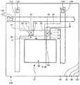
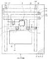
図1は、本発明の第一実施形態にかかる有機EL表示装置の概略ブロック図を示している。
同図において、電気光学装置としての有機EL表示装置1は、データ線駆動回路11、走査線駆動回路12、電源線制御回路13及び電流制御用TFT基板100(適宜、TFT基板100と略称する。)を備えている。また、TFT基板100は、m(列:mは自然数)×n(行:nは自然数)個の画素10がマトリクス状に配設されている。[First Embodiment of Organic EL Display Device]
FIG. 1 shows a schematic block diagram of an organic EL display device according to the first embodiment of the present invention.
In the figure, an organic
データ線駆動回路11は、第1のデータ線111、第2のデータ線112・・・第mのデータ線113を介して、各画素10と接続されており、たとえば、第mのデータ線113を介して、第m列に配設されたn個の画素10と並列に接続されている。このデータ線駆動回路11は、各画素10にデータ信号を出力する。 The data line driving
また、走査線駆動回路12は、第1の走査線121、第2の走査線122・・・第nの走査線123を介して、各画素10と接続されており、たとえば、第nの走査線123を介して、第n行に配設されたm個の画素10と並列に接続されている。この走査線駆動回路12は、各画素10に走査信号を出力する。 The scanning
さらに、電源線制御回路13は、第1のEL駆動線131、第2のEL駆動線132・・・第mのEL駆動線133を介して、各画素10と接続されており、たとえば、第mのEL駆動線133を介して、第m列に配設された画素10と並列に接続されている。この電源線制御回路13は、各画素10に駆動電流を供給する。 Further, the power supply
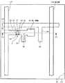
次に、画素10の構成について、図面を参照して説明する。
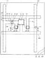
図2は、本発明の第一実施形態にかかる有機EL表示装置の画素の構成を説明するための概略ブロック図を示している。
同図において、画素10は、スイッチングトランジスタ2、駆動トランジスタ3及び有機EL素子4を有している。また、スイッチングトランジスタ2及び駆動トランジスタ3は、薄膜トランジスタとして、TFT基板100上に形成される。
スイッチングトランジスタ2は、ゲート線21を介して走査線120と接続され、ソース線22を介してデータ線110と接続され、ドレイン線23が、駆動トランジスタ3のゲート線31と接続されている。また、駆動トランジスタ3は、ソース線32を介してEL駆動線130と接続され、ドレイン線33を介して有機EL素子4と接続されている。Next, the configuration of the
FIG. 2 is a schematic block diagram for explaining the configuration of the pixel of the organic EL display device according to the first embodiment of the present invention.
In the figure, a
The switching
上記構成のTFT基板100は、走査線120からスイッチングトランジスタ2のゲート信号(走査信号)が入力されると、スイッチングトランジスタ2がonの状態となる。続いて、データ線110からデータ信号(駆動トランジスタ3のゲート電圧)が駆動トランジスタ3のゲート電極34に印加され、駆動トランジスタ3がonの状態となる。このゲート電圧に応じて駆動トランジスタ3のソース・ドレイン間の抵抗値が決定され、EL駆動線130から有機EL素子4に、データ信号に応じた駆動電流が供給され、この駆動電流に応じた輝度で有機EL素子4が発光する。
なお、本実施形態のアクティブマトリクス構成は、基本的な構成としてあるが、この構成に限定されるものではなく、たとえば、駆動トランジスタ3のon状態に保持するためのキャパシタなどを設けた構成としてもよい。In the
The active matrix configuration of the present embodiment is a basic configuration, but is not limited to this configuration. For example, a configuration in which a capacitor for holding the driving
また、本発明の有機EL表示装置1は、駆動トランジスタ3の活性層を、酸化物半導体層としてのn型酸化物半導体層371としてある。このようにすると、駆動トランジスタ3に大きな電流や大電力を投入した場合であっても、駆動トランジスタ3の活性層にアモルファスSiやポリSi半導体を用いたものと比べると、その性能劣化が小さく、安定性に優れるとともに、TFT基板100の耐久性を向上させることができる。したがって、有機EL表示装置1の寿命を大きく延ばすことができる。
次に、上記TFT基板100の製造方法及び構成について、図面を参照して説明する。まず、TFT基板100の製造方法について説明する。In the organic
Next, a manufacturing method and configuration of the
[電流制御用TFT基板の製造方法の第一実施形態]
図3は、本発明の第一実施形態にかかる有機EL表示装置に使用させるTFT基板の製造方法を説明するための概略フローチャート図を示している。なお、本実施形態の製造方法は、請求項16に対応している。
同図において、まず、基板上に、金属層210及び第一のレジスト211をこの順に積層し、第一のマスク212によって、走査線120、スイッチングトランジスタ2のゲート電極24及びゲート線21を形成する(ステップS1)。
次に、第一のマスク212を用いた処理について、図面を参照して説明する。[First Embodiment of Manufacturing Method of Current Control TFT Substrate]
FIG. 3 is a schematic flowchart for explaining a method of manufacturing a TFT substrate used in the organic EL display device according to the first embodiment of the present invention. The manufacturing method according to the present embodiment corresponds to claim 16.
In the figure, first, a
Next, processing using the
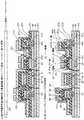
(第一のマスクを用いた処理)
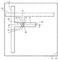
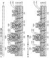
図4は、本発明の第一実施形態にかかる有機EL表示装置に使用させるTFT基板の製造方法の、第一のマスクを用いた処理を説明するための概略図であり、(a)は金属層成膜/第一のレジスト塗布/露光/現像された断面図を、(b)は第一のエッチング/第一のレジスト剥離された断面図を、(c)は第一のレジストが剥離された後のTFT基板の要部の平面図を示している。
同図(a)において、まず、透光性のガラス基板101が用意される。
なお、TFT基板100の基材となる板状部材は、上記ガラス基板101に限定されるものではなく、たとえば、樹脂製の板状部材やシート状部材などでもよい。使用される樹脂として、ポリアクリル樹脂、ポリスチレン樹脂、ポリカーボネート樹脂、ポリアリレート樹脂などを挙げることができる。また、ポリカーボネート樹脂、ポリアリレート樹脂などの耐熱樹脂が好適である。また、透光性の基材に限定されるものではなく、たとえば、遮光性や半透明の基材でもよい。(Process using the first mask)
FIG. 4 is a schematic view for explaining a process using a first mask in a method for manufacturing a TFT substrate used in the organic EL display device according to the first embodiment of the present invention. FIG. (B) is a sectional view of the first etching / first resist stripped, (c) is a stripped of the first resist. The top view of the principal part of the TFT substrate after having been shown is shown.
In FIG. 1A, first, a
In addition, the plate-shaped member used as the base material of
まず、ガラス基板101上に、Al(アルミニウム)とMo(モリブデン)をこれらの順に高周波スパッタリング法を用いて、それぞれ膜厚約250nm、50nmに積層し、走査線120、ゲート電極24及びゲート線21を形成するための、導電体層としての金属層210を形成する。また、Mo以外の金属としては、Ti(チタン),Cr(クロム)などを使用することができる。
なお、ゲート線21として、Ag(銀)、Cu(銅)などの金属薄膜や合金薄膜を用いることもできるが、Al系がよい。また、Alは純粋Alでもよいが、Nd(ネオジウム)、Ce(セリウム)、Mo、W(タングステン)、Nb(ニオブ)などの金属が添加されていてもよい。Ce、W、Nbなどは、透明導電体層との電池反応を抑える上でも好適である。添加量は、適宜選択できるが、約0.1〜2wt%が好ましい。First, Al (aluminum) and Mo (molybdenum) are laminated on the
As the
次に、金属層210上に、第一のレジスト211が塗布され、第一のマスク212を用いて、ホトリソグラフィー法により、所定の形状に第一のレジスト211を形成する。 Next, a first resist 211 is applied on the
次に、同図(b)に示すように、金属層210を、燐酸、酢酸、硝酸及び水からなるエッチング液(体積比は、それぞれ9:8:1:2)を用いて第一のエッチングし、走査線120、ゲート線21及びゲート電極24を形成する(ステップS1)。
続いて、第一のレジスト211をアッシングすると、同図(c)に示すように、ガラス基板101上に、走査線120、並びに、この走査線120と接続されたゲート線21及びゲート電極24が露出する。同図(b)に示す、走査線120は、同図(c)におけるA−A断面を示しており、ゲート電極24は、B−B断面を示している。Next, as shown in FIG. 2B, the
Subsequently, when the first resist 211 is ashed, the
次に、図3に示すように、ガラス基板101、走査線120、ゲート線21及びゲート電極24上に、グロー放電CVD(化学蒸着法)法により、窒化シリコン(SiNx)膜であるゲート絶縁膜20を膜厚約300nm堆積する(ステップS2)。このゲート絶縁膜20は、スイッチングトランジスタ2用のゲート絶縁膜20として形成される。なお、本実施形態では、放電ガスとして、SiH4−NH3−N2系の混合ガスを用いる。Next, as shown in FIG. 3, a gate insulating film that is a silicon nitride (SiNx) film is formed on the
次に、図3に示すように、α−Si:H(i)膜271、α−Si:H(n)膜272、導電体層としての金属層273及び第二のレジスト274を積層し、第二のハーフトーンマスク275によって、データ線110、スイッチングトランジスタ2のソース線22、ソース電極25、チャンネル部27、ドレイン電極26及びドレイン線23、並びに、駆動トランジスタ3のゲート線31及びゲート電極34を形成する(ステップS3)。
次に、第二のハーフトーンマスク275を用いた処理について、図面を参照して説明する。Next, as shown in FIG. 3, an α-Si: H (i)
Next, processing using the second halftone mask 275 will be described with reference to the drawings.
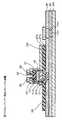
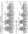
(第二のハーフトーンマスクを用いた処理)
図5は、本発明の第一実施形態にかかる有機EL表示装置に使用させるTFT基板の製造方法の、第二のハーフトーンマスクを用いた処理を説明するための概略図であり、(a)はゲート絶縁膜成膜/α−Si:H(i)膜成膜/α−Si:H(n)膜成膜/金属層成膜/第二のレジスト塗布/ハーフトーン露光/現像された断面図を、(b)は第二のエッチング/第二のレジストの再形成された断面図を、(c)は第三のエッチング/第二のレジスト剥離された断面図を示している。
同図(a)において、ゲート絶縁膜20上に、まず、アモルファスSi(ケイ素)の絶縁層としてのα−Si:H(i)膜271を膜厚約350nm積層する。この際、放電ガスとして、SiH4−N2系の混合ガスを用いる。
次に、アモルファスSiのn型半導体層としてのα−Si:H(n)膜272を、SiH4−H2−PH3系の混合ガスを用いて膜厚約300nm堆積する。続いて、MoとAlとMoを、これらの順に高周波スパッタリング法を用いて膜厚約50nm、250nm、50nm積層し、Mo層/Al層/Mo層からなる金属層273を形成する。なお、金属層273のMo層は、Al層を保護するバリヤー金属層として機能する。また、本実施形態では、スイッチングトランジスタ2の活性層として、アモルファスSiを使用しているが、これに限定されるものではなく、たとえば、多結晶Siを使用してもよい。(Process using second halftone mask)
FIG. 5 is a schematic diagram for explaining a process using a second halftone mask in a method for manufacturing a TFT substrate used in the organic EL display device according to the first embodiment of the present invention. Is gate insulating film deposition / α-Si: H (i) film deposition / α-Si: H (n) film deposition / metal layer deposition / second resist coating / halftone exposure / developed cross section (B) is a cross-sectional view of the second etching / second resist, and (c) is a cross-sectional view of the third etching / second resist removed.
In FIG. 2A, an α-Si: H (i)
Next, an α-Si: H (n)
次に、金属層273上に、第二のレジスト274が塗布され、第二のハーフトーンマスク275及びハーフトーン露光によって、第二のレジスト274を所定の形状に形成する。すなわち、第二のレジスト274は、データ線110、スイッチングトランジスタ2のソース線22、ソース電極25、ゲート電極24、ドレイン電極26、ドレイン線23、駆動トランジスタ3のゲート線31、ゲート電極34を覆い、かつ、ハーフトーンマスク部276によって、チャンネル部27を覆う部分が他の部分より薄い形状に形成される。 Next, a second resist 274 is applied on the
次に、同図(b)に示すように、第二のエッチングとして、まず、第二のレジスト274、並びに、燐酸、酢酸、硝酸及び水からなるエッチング液(体積比は、それぞれ9:8:1:2)を用いて、金属層273をエッチングする。続いて、α−Si:H(n)膜272及びα−Si:H(i)膜271に対して、CHFガスを用いたドライエッチングとヒドラジン水溶液(NH2NH2・H20)を用いたウェットエッチングを併用してエッチングし、データ線110、ソース線22、ドレイン線23、ゲート線31及びゲート電極34を形成する。Next, as shown in FIG. 6B, as the second etching, first, the second resist 274 and an etching solution composed of phosphoric acid, acetic acid, nitric acid and water (volume ratios are 9: 8: 1: 2) is used to etch the
続いて、上記第二のレジスト274をアッシングし、チャンネル部27の上方の金属層273が露出し、かつ、データ線110、スイッチングトランジスタ2のソース線22、ソース電極25、ドレイン電極26、ドレイン線23、駆動トランジスタ3のゲート線31、ゲート電極34が覆われる形状に、第二のレジスト274を再形成する。 Subsequently, the second resist 274 is ashed, the
次に、同図(c)に示すように、第三のエッチングとして、再形成された第二のレジスト274、並びに、燐酸、酢酸、硝酸及び水からなるエッチング液(体積比は、それぞれ9:8:1:2)を用いて、金属層273をエッチングし、ソース電極25及びドレイン電極26を形成する。さらに、α−Si:H(n)膜272に対して、CHFガスを用いたドライエッチングとヒドラジン水溶液(NH2NH2・H20)を用いたウェットエッチングを併用してエッチングし、α−Si:H(i)膜271からなるチャンネル部27を形成するとともに、スイッチングトランジスタ2のソース電極25及びドレイン電極26を形成する(ステップS3)。Next, as shown in FIG. 6C, as the third etching, the re-formed second resist 274 and an etching solution composed of phosphoric acid, acetic acid, nitric acid, and water (volume ratio is 9: 8: 1: 2), the
続いて、再形成された第二のレジスト274をアッシングすると、同図(c)に示すように、ゲート絶縁膜20上に、データ線110、スイッチングトランジスタ2のソース線22、ソース電極25、チャンネル部27、ドレイン電極26、ドレイン線23、駆動トランジスタ3のゲート線31、ゲート電極34が露出する。図5(c)に示す、データ線110、スイッチングトランジスタ2のソース線22、ソース電極25、ゲート電極24、チャンネル部27、ドレイン電極26、ドレイン線23、駆動トランジスタ3のゲート線31、ゲート電極34は、図6におけるC−C断面を示している。 Subsequently, when the re-formed second resist 274 is ashed, the
次に、図3に示すように、ガラス基板101の上方に、グロー放電CVD(化学蒸着法)法により、窒化シリコン(SiNx)膜であるゲート絶縁膜30を膜厚約300nm堆積する。このゲート絶縁膜30は、駆動トランジスタ3用のゲート絶縁膜30として形成される。なお、本実施形態では、放電ガスとして、SiH4−NH3−N2系の混合ガスを用いる。Next, as shown in FIG. 3, a
次に、図3に示すように、ゲート絶縁膜30上に、酸化物半導体層としてのn型酸化物半導体層371及び第三のレジスト372を積層し、第三のマスク373によって、駆動トランジスタ3の活性層を形成する(ステップS5)。
次に、第三のマスク373を用いた処理について、図面を参照して説明する。Next, as illustrated in FIG. 3, an n-type
Next, treatment using the third mask 373 will be described with reference to the drawings.
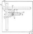
(第三のマスクを用いた処理)
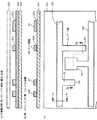
図7は、本発明の第一実施形態にかかる有機EL表示装置に使用させるTFT基板の製造方法の、第三のマスクを用いた処理を説明するための概略図であり、(a)はゲート絶縁膜成膜/n型酸化物半導体層成膜/第三のレジスト塗布/露光/現像された断面図を、(b)は第四のエッチング/第三のレジスト剥離された断面図を示している。
同図において、ゲート絶縁膜30上に、酸化インジウム−酸化亜鉛(In2O3:ZnO=約97:3wt%)のターゲットを用い、所定の酸素:アルゴン比(約10:90Vol.%)状態に維持しつつ基板温度約100℃未満の条件にて、膜厚約150nmのn型酸化物半導体層371を成膜する。この条件では、n型酸化物半導体層371は、非晶質膜として得られる。通常、200℃以下の低温で成膜した場合は、非晶質膜として得られ、200℃を超える高温で成膜した場合、結晶質膜として得られる。また、非晶質膜は、熱処理により結晶化させることもでき、本実施形態では、結晶化させて用いる。(Process using third mask)
FIG. 7 is a schematic view for explaining a process using a third mask in a method of manufacturing a TFT substrate used in the organic EL display device according to the first embodiment of the present invention, and FIG. Insulating film deposition / n-type oxide semiconductor layer deposition / third resist coating / exposure / development sectional view, (b) shows fourth etching / third resist stripped sectional view Yes.
In the figure, a target of indium oxide-zinc oxide (In2 O3 : ZnO = about 97: 3 wt%) is used on the
なお、n型酸化物半導体層371は、上記酸化インジウム−酸化亜鉛からなる酸化物半導体層に限定されるものではなく、たとえば、酸化インジウム−酸化ガリウム−酸化亜鉛系や、酸化インジウム−酸化サマリウム、酸化亜鉛−酸化マグネシウムなどからなる酸化物半導体層としてもよい。
また、本実施形態における酸化インジウム−酸化亜鉛薄膜のキャリヤー密度は、10+16cm−3以下であり、十分に半導体として作動する領域であった。また、ホール移動度は、25cm2/V・secであった。キャリヤー密度は10+17cm−3台未満であれば、十分に作動領域になり、かつ、移動度は、非晶質シリコンのそれに比べて10倍以上大きく、十分に有用な半導体薄膜である。通常、酸化物半導体は、ホール移動度が10cm2/V・sec以上であることが望ましく、さらに好適には、50cm2/V・sec以上であることが望ましい。このように、アモルファスSiより高移動度の酸化物半導体を用いることにより、大電流の投入による発熱や応答速度の遅延がなくなり、安定した駆動が可能となる。Note that the n-type
In addition, the carrier density of the indium oxide-zinc oxide thin film in this embodiment is 10+16 cm−3 or less, which is a region that operates sufficiently as a semiconductor. The hole mobility was 25 cm2 / V · sec. If the carrier density is less than 10+17 cm−3 , it is a sufficiently useful semiconductor thin film, and the mobility is more than 10 times larger than that of amorphous silicon. In general, the oxide semiconductor desirably has a hole mobility of 10 cm2 / V · sec or more, and more preferably 50 cm2 / V · sec or more. As described above, by using an oxide semiconductor having a higher mobility than amorphous Si, heat generation and response speed delay due to input of a large current are eliminated, and stable driving is possible.
また、n型酸化物半導体層371は、透明性が必要なことから、エネルギーギャップは、約3.0eV以上の酸化物を用いるとよい。好ましくは約3.2eV以上、より好ましくは約3.4eV以上である。上記の酸化インジウム−酸化亜鉛系、酸化インジウム−酸化ガリウム−酸化亜鉛系や、酸化インジウム−酸化サマリウム、酸化亜鉛−酸化マグネシウムなどからなるn型酸化物半導体層のエネルギーギャップは、3.2eV以上であり、好適に使用される。
また、n型酸化物半導体層371は、非晶質の場合、蓚酸水溶液や燐酸、酢酸及び硝酸からなる混酸に溶解可能であるが、加熱結晶化させることにより、蓚酸水溶液や燐酸、酢酸及び硝酸からなる混酸に不溶となり、耐性を示すようになる。また、結晶化の温度は、添加する酸化亜鉛の量により制御できる。Since the n-type
In addition, the n-type
続いて、n型酸化物半導体層371上に、第三のレジスト372を塗布し、第三のマスク373及び露光技術を用いて、ゲート電極34の上方に、第三のレジスト372を形成する。 Subsequently, a third resist 372 is applied over the n-type
次に、同図(b)に示すように、第四のエッチングとして、まず、第三のレジスト372及び蓚酸水溶液を用いて、n型酸化物半導体層371をエッチングし、n型酸化物半導体層371からなる駆動トランジスタ3の活性層を形成する。続いて、第三のレジスト372をアッシングし、n型酸化物半導体層371を露出させる。図7(b)に示すゲート電極34及びn型酸化物半導体層371は、図8におけるD−D断面を示している。
なお、本実施形態では、理解しやすいように、ドレイン線23とゲート線31及びゲート電極34を接続し、ゲート電極34の上方にn型酸化物半導体層371を形成してあるが、これに限定されるものではなく、たとえば、n型酸化物半導体層371をスイッチングトランジスタ2のドレイン電極26の上方に形成してもよい。また、n型酸化物半導体層371を形成したところで、約180℃以上の温度にて、TFT基板100を熱処理し、n型酸化物半導体371の活性層を結晶化する。熱処理温度は、約150℃以上あれば、問題ないが、好ましくは約200℃以上が好適である。また、上記熱処理温度は、ガラス基板100や樹脂基板が変形しない温度とする必要がある。Next, as shown in FIG. 4B, as the fourth etching, first, the n-type
In the present embodiment, for easy understanding, the
次に、図3に示すように、酸化物導電体層としての酸化物透明導電体層374、補助導電体層(補助金属層)としての金属層375及び第四のレジスト376を積層し、第四のハーフトーンマスク377によって、EL駆動線130、駆動トランジスタ3のソース線32、ソース電極35、チャンネル部37、ドレイン電極36及びドレイン線33、並びに、画素電極38を形成する(ステップS6)。
次に、第四のハーフトーンマスク377を用いた処理について、図面を参照して説明する。Next, as shown in FIG. 3, an oxide
Next, processing using the
(第四のハーフトーンマスクを用いた処理)
図9は、本発明の第一実施形態にかかる有機EL表示装置に使用させるTFT基板の製造方法の、第四のハーフトーンマスクを用いた処理を説明するための概略図であり、(a)は酸化物透明導電体層成膜/金属層成膜/第四のレジスト塗布/ハーフトーン露光/現像された断面図を、(b)は第五のエッチング/第四のレジストの再形成された断面図を示している。
同図(a)において、露出したゲート絶縁膜30及びn型酸化物半導体層371上に、まず、酸化インジウム−酸化スズ−酸化亜鉛(In2O3:SnO2:ZnO=約60:20:20wt%)ターゲットを用いて、高周波スパッタリング法により、酸素約1%、アルゴン約99%、さらに、酸化物透明導電体層374を結晶化させない条件で厚み約120nmの酸化物透明導電体層374を形成する。(Process using the fourth halftone mask)
FIG. 9 is a schematic diagram for explaining a process using a fourth halftone mask in a method for manufacturing a TFT substrate used in the organic EL display device according to the first embodiment of the present invention. Is a sectional view of oxide transparent conductor layer deposition / metal layer deposition / fourth resist coating / halftone exposure / development, (b) fifth etching / fourth resist re-formation A cross-sectional view is shown.
In FIG. 6A, on the exposed
ここで、上記酸化インジウム−酸化スズ−酸化亜鉛からなる酸化物透明導電体層374は、非晶質でありながら、蓚酸水溶液には溶解するが、燐酸、酢酸及び硝酸からなる混酸には溶解しないので、有用である。このとき、酸化スズの含有量は、約10〜40重量%であり、酸化亜鉛は約10〜40重量%、残りが酸化インジウムとするとよい。酸化スズ及び酸化亜鉛がそれぞれ約10重量%未満では、燐酸、酢酸及び硝酸からなる混酸への耐性がなくなり、溶解するようになる。また、酸化スズが約40重量%を超えると、蓚酸水溶液に溶解しなくなったり、比抵抗が大きくなったりする。また、酸化亜鉛が約40重量%を超えると、燐酸、酢酸及び硝酸からなる混酸への耐性が無くなったりする場合がある。酸化スズと酸化亜鉛の比は適宜選択すればよい。 Here, the oxide
また、酸化物透明導電体層374は、本実施形態で用いた酸化インジウム−酸化スズ−酸化亜鉛系の透明導電膜に限定されるものではなく、蓚酸水溶液でエッチングが可能であり、かつ、燐酸、酢酸及び硝酸からなる混酸に溶解しない透明導電膜であれば用いることができる。
また、非晶質状態では、蓚酸水溶液や、燐酸、酢酸及び硝酸からなる混酸に溶解する場合でも、加熱などにより結晶化などの膜質変化をもたらし、燐酸、酢酸及び硝酸からなる混酸に不溶となれば使用可能となる。このような透明導電膜としては、酸化インジウムに、酸化スズ、酸化ゲルマニウム、酸化ジルコニウム、酸化タングステン、酸化モリブデン、酸化セリウムなどのランタノイド系元素を含むものが挙げられる。これらのなかでも、酸化インジウムと酸化スズ、酸化インジウムと酸化タングステン、酸化インジウムと酸化セリウムなどの酸化ランタノイド系元素の組合せは好適に用いられる。添加する金属の量としては、酸化インジウムに対して約1〜20wt%、好ましくは約3〜15wt%である。約1wt%未満では、成膜時に結晶化し、蓚酸水溶液に溶解しなくなったり、比抵抗が大きくなり、透明導電膜として好適に使用できないものになったりする場合がある。約20wt%を超えると、加熱などにより結晶化などの膜質変化を起こさせる場合に、膜質変化が起きず、燐酸、酢酸及び硝酸からなる混酸に溶解し、画素電極38の形成が難しくなるなどの問題が発生することがある。The oxide
In the amorphous state, even when dissolved in an aqueous oxalic acid solution or a mixed acid composed of phosphoric acid, acetic acid and nitric acid, it causes film quality changes such as crystallization due to heating, etc., and becomes insoluble in a mixed acid composed of phosphoric acid, acetic acid and nitric acid. Can be used. Examples of such a transparent conductive film include those containing lanthanoid elements such as tin oxide, germanium oxide, zirconium oxide, tungsten oxide, molybdenum oxide, and cerium oxide in indium oxide. Among these, combinations of lanthanoid oxide elements such as indium oxide and tin oxide, indium oxide and tungsten oxide, indium oxide and cerium oxide are preferably used. The amount of the metal to be added is about 1 to 20 wt%, preferably about 3 to 15 wt% with respect to indium oxide. If it is less than about 1 wt%, it may crystallize at the time of film formation and may not be dissolved in the oxalic acid aqueous solution, or the specific resistance may increase, and it may not be suitable for use as a transparent conductive film. If it exceeds about 20 wt%, when film quality change such as crystallization is caused by heating or the like, the film quality change does not occur, but it dissolves in a mixed acid composed of phosphoric acid, acetic acid and nitric acid, making it difficult to form the
続いて、MoとAlとMoを、これらの順に高周波スパッタリング法を用いて膜厚約50nm、250nm、50nm積層し、Mo層/Al層/Mo層からなる補助導電体層としての金属層375を形成する。
次に、金属層375上に、第四のレジスト376が塗布され、第四のハーフトーンマスク377及びハーフトーン露光によって、第四のレジスト376を所定の形状に形成する。すなわち、第四のレジスト376は、EL駆動線130、駆動トランジスタ3のソース線32、ソース電極35、ドレイン電極36、ドレイン線33、画素電極38を覆い、かつ、ハーフトーンマスク部378によって、画素電極38を覆う部分が他の部分より薄い形状に形成される。Subsequently, Mo, Al, and Mo are laminated in this order using a high-frequency sputtering method to a film thickness of about 50 nm, 250 nm, and 50 nm, and a
Next, a fourth resist 376 is applied on the
次に、同図(b)に示すように、第五のエッチングとして、まず、第四のレジスト376、並びに、燐酸、酢酸、硝酸及び水からなるエッチング液(体積比は、それぞれ9:8:1:2)を用いて、金属層375をエッチングする。続いて、第四のレジスト376及び蓚酸水溶液を用いて、酸化物透明導電体層374をエッチングし、EL駆動線130、駆動トランジスタ3のソース線32、ソース電極35、チャンネル部37、ドレイン電極36、ソース線32、画素電極38を形成する(ステップS6)。 Next, as shown in FIG. 5B, as the fifth etching, first, a fourth resist 376 and an etching solution composed of phosphoric acid, acetic acid, nitric acid, and water (volume ratios are 9: 8: 1: 2) is used to etch the
続いて、上記第四のレジスト376をアッシングし、画素電極38の上方の金属層375が露出し、かつ、EL駆動線130、駆動トランジスタ3のソース線32、ソース電極35、ドレイン電極36、ドレイン線33が覆われる形状に、第四のレジスト376を再形成する。
なお、本実施形態では、補助導電体層としての金属層375を積層しているので、第四のハーフトーンマスク377を使用しているが、金属層375を積層しない場合には、第四のマスクを使用することができる。Subsequently, the fourth resist 376 is ashed to expose the
In the present embodiment, since the
図10は、本発明の第一実施形態にかかる有機EL表示装置に使用させるTFT基板の製造方法の、第四のハーフトーンマスクを用いた処理を説明するための概略図であり、第六のエッチング/第四のレジスト剥離された断面図を示している。
同図において、第六のエッチングとして、再形成された第四のレジスト376、並びに、燐酸、酢酸、硝酸及び水からなるエッチング液(体積比は、それぞれ9:8:1:2)を用いて、金属層375をエッチングし、画素電極38を露出させる。なお、有機EL表示装置1がトップエミッション構造などの場合には、画素電極38上の金属層375を除去する必要はなく、第四のハーフトーンマスク377の代わりに、第四のマスクを用いることができる。FIG. 10 is a schematic diagram for explaining a process using a fourth halftone mask in a method for manufacturing a TFT substrate used in the organic EL display device according to the first embodiment of the present invention. FIG. 10 shows a cross-sectional view after etching / fourth resist peeling.
In the figure, as the sixth etching, a re-formed fourth resist 376 and an etching solution made of phosphoric acid, acetic acid, nitric acid and water (volume ratios are 9: 8: 1: 2 respectively) are used. The
続いて、再形成された第四のレジスト376をアッシングすると、同図に示すように、ゲート絶縁膜30上に、EL駆動線130、駆動トランジスタ3のソース線32、ソース電極35、チャンネル部37、ドレイン電極36、ドレイン線33、画素電極38が露出する。図10に示す、EL駆動線130、駆動トランジスタ3のソース線32、ソース電極35、ゲート電極34、チャンネル部37、ドレイン電極36、ドレイン線33、画素電極38は、図11におけるE−E断面を示している。 Subsequently, when the re-formed fourth resist 376 is ashed, the
次に、図3に示すように、保護用絶縁膜40及び第五のレジスト41を積層し、第五のマスクによって、走査線用パッド124、データ線用パッド114、EL駆動線用パッド134及び画素電極38を露出させる(ステップS7)。
次に、第五のマスク42を用いた処理について、図面を参照して説明する。Next, as shown in FIG. 3, a protective insulating
Next, processing using the
(第五のマスクを用いた処理)
図12は、本発明の第一実施形態にかかる有機EL表示装置に使用させるTFT基板の製造方法の、第五のマスクを用いた処理を説明するための概略図であり、(a)は保護用絶縁膜成膜/第五のレジスト塗布/露光/現像された断面図を、(b)は第七のエッチング/第五のレジスト剥離された断面図を示している。
同図(a)において、ガラス基板101の上方に、グロー放電CVD(化学蒸着法)法により、窒化シリコン(SiNx)膜である保護用絶縁膜40を膜厚約250nm堆積する。なお、本実施形態では、放電ガスとして、SiH4−NH3−N2系の混合ガスを用いる。(Process using the fifth mask)
FIG. 12 is a schematic diagram for explaining a process using a fifth mask in a method for manufacturing a TFT substrate used in the organic EL display device according to the first embodiment of the present invention, and FIG. Insulating film formation / fifth resist coating / exposure / development sectional view, (b) shows a seventh etching / fifth resist stripped sectional view.
In FIG. 6A, a protective insulating
次に、保護用絶縁膜40上に、第五のレジスト41を塗布し、第五のマスク42及び露光技術を用いて、画素電極38、データ線用パッド114、走査線用パッド124及びEL駆動線用パッド134の上方に、開口部を有する第五のマスク42を形成する。
続いて、第七のエッチングとして、CHF(CF4,CHF3など)ガスを用いたドライエッチングにより、保護用絶縁膜40、ゲート絶縁膜30、ゲート絶縁膜20をエッチングし、画素電極38、データ線用パッド114、走査線用パッド124及びEL駆動線用パッド134を露出させる(ステップS7)。Next, a fifth resist 41 is applied on the protective insulating
Subsequently, as the seventh etching, the protective insulating
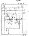
続いて、第五のレジスト41をアッシングすると、同図に示すように、保護用絶縁膜40が露出する。図12(b)に示す、画素電極38、駆動トランジスタ3のソース線32、ソース電極35、ゲート電極34、チャンネル部37、ドレイン電極36、ドレイン線33は、図13におけるF−F断面を示している。
なお、本実施形態では、スイッチングトランジスタ2、駆動トランジスタ3及び画素電極38の位置や形状を、理解しやすい位置や形状としてあるが、これに限定されるものではない。Subsequently, when the fifth resist 41 is ashed, the protective insulating
In the present embodiment, the positions and shapes of the switching
このように、本実施形態の電流制御用TFT基板の製造方法によれば、駆動トランジスタ3の活性層をn型酸化物半導体層371としてあるので、駆動トランジスタ3に大きな電流や大電力を投入した場合であっても、駆動トランジスタ3の性能劣化が小さく、安定性に優れるとともに、TFT基板100の耐久性を向上させることができる。また、第四のハーフトーンマスク377を用いて、EL駆動線130、駆動トランジスタ3のソース線32、ソース電極35、チャンネル部37、ドレイン電極36、ドレイン線33、画素電極38を製造することができ、使用するマスク数を削減できるので、製造工程が削減されることにより、生産効率が向上し製造原価のコストダウンを図ることができる。さらに、保護用絶縁膜40が形成されているので、TFT基板100に、有機EL材料,電極及び保護膜を設けることにより、有機EL表示装置1を容易に得ることができる。
次に、上記TFT基板100の構成について、図面を参照して説明する。As described above, according to the method for manufacturing the current control TFT substrate of the present embodiment, since the active layer of the
Next, the configuration of the
[電流制御用TFT基板の第一実施形態]
本実施形態のTFT基板100は、図1に示すように、ガラス基板101に、m(列:mは自然数)×n(行:nは自然数)個の画素10がマトリクス状に配設されている。
また、行方向(水平方向)に、n本の走査線121、122・・・123が形成され、たとえば、第nの走査線123は、第n行に配設されたm個の画素10と並列に接続されている。
また、列方向(垂直方向)に、m本のデータ線111、112・・・113が形成され、たとえば、第mのデータ線113を介して、第m列に配設されたn個の画素10と並列に接続されている。
さらに、列方向(垂直方向)に、m本のEL駆動線131、132・・・133が形成され、たとえば、第mのEL駆動線133を介して、第m列に配設された画素10と並列に接続されている。[First embodiment of current control TFT substrate]
As shown in FIG. 1, in the
In addition,
In addition, m data lines 111, 112,... 113 are formed in the column direction (vertical direction). For example, n pixels arranged in the mth column via the mth data line 113. 10 is connected in parallel.
Further, m EL drive
また、各画素10は、図13に示すように、電気光学素子である有機EL素子4(図2参照)に電流を供給する駆動トランジスタ3と、この駆動トランジスタ3を制御するスイッチングトランジスタ2を有している。 Further, as shown in FIG. 13, each
スイッチングトランジスタ2は、図5及び図6に示すように、ゲート線21を介して走査線120と接続されたゲート電極24と、ゲート電極24上に形成されたゲート絶縁膜20と、このゲート絶縁膜20上に形成された活性層としてのα−Si:H(i)膜271およびα−Si:H(n)膜272と、ソース線22を介してデータ線110と接続されたソース電極25と、ドレイン線23およびゲート線31を介して駆動トランジスタ3のゲート電極34と接続されたドレイン電極26を備えている。 As shown in FIGS. 5 and 6, the switching
駆動トランジスタ3は、図10及び図11に示すように、ゲート電極34と、ゲート電極34上に形成されたゲート絶縁膜30と、このゲート絶縁膜30上に形成された活性層としてのn型酸化物半導体層371と、ソース線32を介してEL駆動線130と接続されたソース電極35と、ドレイン線33を介して画素電極38と接続されたドレイン電極36を備えている。 As shown in FIGS. 10 and 11, the driving
また、駆動トランジスタ3は、ソース線32、ソース電極35、ドレイン電極36、ドレイン線33が、酸化物透明導電体層374からなり、この酸化物透明導電体層374が、有機EL素子4の画素電極38を兼ねている。このようにすると、製造する際に使用するマスク数を削減でき、製造工程が削減されることにより、生産効率が向上し製造原価のコストダウンを図ることができる。
なお、「酸化物透明導電体層374が、画素電極38を兼ねる」とは、形成された酸化物透明導電体層374が、画素電極38としての機能を有することをいう。Further, in the
Note that “the oxide
また、好ましくは、EL駆動線130、ソース線32、ソース電極35、ドレイン電極36、ドレイン線33の上方に、補助導電体層としての金属層375を形成するとよい。このようにすると、各線や電極の電気抵抗を低減することができ、信頼性を向上させることができるとともに、エネルギー効率の低下を抑制することができる。 Preferably, a
このように、本実施形態のTFT基板100は、駆動トランジスタ3の活性層をn型酸化物半導体層371としてあるので、駆動トランジスタ3に大きな電流や大電力を投入した場合であっても、駆動トランジスタ3の性能劣化が小さく、安定性に優れるとともに、TFT基板100の耐久性を向上させることができる。
また、上述した有機EL表示装置の第一実施形態、電流制御用TFT基板の製造方法の第一実施形態、及び、電流制御用TFT基板の第一実施形態は、様々な応用例を有している。たとえば、上記各実施形態では、スイッチングトランジスタ2の活性層として、α−Si:H(i)膜271を用いているが、α−Si:H(i)膜271の代わりに、酸化物半導体層を用いてもよい。
次に、α−Si:H(i)膜271の代わりに、酸化物半導体層を用いた電流制御用TFT基板の製造方法の応用例について、図面を参照して説明する。As described above, the
In addition, the first embodiment of the organic EL display device, the first embodiment of the method for manufacturing the current control TFT substrate, and the first embodiment of the current control TFT substrate have various application examples. Yes. For example, in each of the above embodiments, the α-Si: H (i)
Next, an application example of a method for manufacturing a current control TFT substrate using an oxide semiconductor layer instead of the α-Si: H (i)
[電流制御用TFT基板の製造方法の応用例]
図14は、本発明の第一実施形態の応用例にかかる有機EL表示装置に使用させるTFT基板の製造方法を説明するための概略フローチャート図を示している。なお、本応用例の製造方法は、請求項13に対応している。
同図において、本応用例のTFT基板の製造方法は、上述した第一実施形態と比べて、ステップS4(図3参照)の代わりに、n型酸化物半導体層271´、酸化物透明導電体層272´、金属層273及び第二のレジスト274を積層し、第二のハーフトーンマスク275によって、データ線110´、スイッチングトランジスタ2´のソース線22´、ソース電極25´、チャンネル部27´、ドレイン電極26´及びドレイン線23´、並びに、駆動トランジスタ3のゲート線31´及びゲート電極34´を形成する(ステップS3´)点が相違する。他の方法は第一実施形態とほぼ同様としてある。
したがって、図14において、図3と同様の方法については同一の符号を付して、その詳細な説明を省略する。
次に、第二のハーフトーンマスク275を用いた処理について、図面を参照して説明する。[Application example of manufacturing method of current control TFT substrate]
FIG. 14: has shown the schematic flowchart figure for demonstrating the manufacturing method of the TFT substrate used for the organic electroluminescent display apparatus concerning the application example of 1st embodiment of this invention. The manufacturing method of this application example corresponds to claim 13.
In this figure, the manufacturing method of the TFT substrate of this application example is different from that in the first embodiment described above, in place of step S4 (see FIG. 3), n-type
Therefore, in FIG. 14, the same reference numerals are given to the same methods as in FIG. 3, and the detailed description thereof is omitted.
Next, processing using the second halftone mask 275 will be described with reference to the drawings.
(第二のハーフトーンマスクを用いた処理)
図15は、本発明の第一実施形態の応用例にかかる有機EL表示装置に使用させるTFT基板の製造方法の、第二のハーフトーンマスクを用いた処理を説明するための概略図であり、(a)はゲート絶縁膜成膜/n型酸化物半導体層成膜/酸化物透明導電体層成膜/金属層成膜/第二のレジスト塗布/ハーフトーン露光/現像された断面図を、(b)は第二のエッチング/第二のレジストの再形成された断面図を、(c)は第三のエッチング/第二のレジスト剥離された断面図を示している。
同図(a)において、ゲート絶縁膜20上に、酸化インジウム−酸化亜鉛(In2O3:ZnO=約97:3wt%)のターゲットを用い、所定の酸素:アルゴン比(約10:90Vol.%)状態に維持しつつ基板温度約100℃未満の条件にて、膜厚約150nmのn型酸化物半導体層271´を成膜する。この条件では、n型酸化物半導体層271´は、非晶質膜として得られる。(Process using second halftone mask)
FIG. 15 is a schematic diagram for explaining a process using a second halftone mask in a method of manufacturing a TFT substrate used in the organic EL display device according to the application example of the first embodiment of the present invention. (A) is a cross-sectional view of gate insulating film deposition / n-type oxide semiconductor layer deposition / oxide transparent conductor layer deposition / metal layer deposition / second resist coating / halftone exposure / development, (B) is a cross-sectional view of the second etching / second resist, and (c) is a cross-sectional view of the third etching / second resist removed.
In FIG. 7A, a target of indium oxide-zinc oxide (In2 O3 : ZnO = about 97: 3 wt%) is used on the
次に、n型酸化物半導体層271´上に、まず、酸化インジウム−酸化スズ−酸化亜鉛(In2O3:SnO2:ZnO=約60:20:20wt%)ターゲットを用いて、高周波スパッタリング法により、酸素約1%、アルゴン約99%、さらに、酸化物透明導電体層272´を結晶化させない条件で厚み約120nmの酸化物透明導電体層272´を形成する。続いて、MoとAlとMoを、これらの順に高周波スパッタリング法を用いて膜厚約50nm、250nm、50nm積層し、Mo層/Al層/Mo層からなる、補助導電体層としての金属層273を形成する。なお、金属層273のMo層は、Al層を保護するバリヤー金属層として機能する。Next, high-frequency sputtering is first performed on the n-type
次に、金属層273上に、第二のレジスト274が塗布され、第二のハーフトーンマスク275及びハーフトーン露光によって、第二のレジスト274を所定の形状に形成する。すなわち、第二のレジスト274は、データ線110´、スイッチングトランジスタ2のソース線22´、ソース電極25´、ゲート電極24、ドレイン電極26´、ドレイン線23´、駆動トランジスタ3のゲート線31´、ゲート電極34´を覆い、かつ、ハーフトーンマスク部276によって、チャンネル部27´を覆う部分が他の部分より薄い形状に形成される。 Next, a second resist 274 is applied on the
次に、同図(b)に示すように、第二のエッチングとして、まず、第二のレジスト274、並びに、燐酸、酢酸、硝酸及び水からなるエッチング液(体積比は、それぞれ9:8:1:2)を用いて、金属層273をエッチングする。続いて、酸化物透明導電体層272´及びn型酸化物半導体層271´に対して、蓚酸水溶液を用いてエッチングし、データ線110´、ソース線22´、ドレイン線23´、ゲート線31´及びゲート電極34´を形成する。
ここで、n型酸化物半導体層271´を熱処理により結晶化させる。これにより、燐酸、酢酸、硝酸及び水からなるエッチング液(体積比は、それぞれ9:8:1:2)や蓚酸水溶液に対して、n型酸化物半導体層271´が耐性を有する。Next, as shown in FIG. 6B, as the second etching, first, the second resist 274 and an etching solution composed of phosphoric acid, acetic acid, nitric acid and water (volume ratios are 9: 8: 1: 2) is used to etch the
Here, the n-type
続いて、上記第二のレジスト274をアッシングし、チャンネル部27´の上方の金属層273が露出し、かつ、データ線110´、スイッチングトランジスタ2´のソース線22´、ソース電極25´、ドレイン電極26´、ドレイン線23´、駆動トランジスタ3のゲート線31´、ゲート電極34´が覆われる形状に、第二のレジスト274を再形成する。 Subsequently, the second resist 274 is ashed to expose the
次に、同図(c)に示すように、第三のエッチングとして、再形成された第二のレジスト274、並びに、燐酸、酢酸、硝酸及び水からなるエッチング液(体積比は、それぞれ9:8:1:2)を用いて、金属層273及び酸化物透明導電体層272´をエッチングし、チャンネル部27´、ソース電極25´及びドレイン電極26´を形成する(ステップS3´)。 Next, as shown in FIG. 6C, as the third etching, the re-formed second resist 274 and an etching solution composed of phosphoric acid, acetic acid, nitric acid, and water (volume ratio is 9: 8: 1: 2), the
続いて、再形成された第二のレジスト274をアッシングすると、同図(c)に示すように、ゲート絶縁膜20上に、データ線110´、スイッチングトランジスタ2´のソース線22´、ソース電極25´、チャンネル部27´、ドレイン電極26´、ドレイン線23´、駆動トランジスタ3のゲート線31´、ゲート電極34´が露出する。図15(c)に示す、データ線110´、スイッチングトランジスタ2´のソース線22´、ソース電極25´、ゲート電極24、チャンネル部27´、ドレイン電極26´、ドレイン線23´、駆動トランジスタ3のゲート線31´、ゲート電極34´は、図16におけるC´−C´断面を示している。
なお、その他の方法は、上記第一実施形態とほぼ同様としてある。Subsequently, when the re-formed second resist 274 is ashed, the
Other methods are almost the same as those in the first embodiment.
このように、本応用例の電流制御用TFT基板の製造方法によれば、上記第一実施形態の製造方法とほぼ同様の効果を有するとともに、駆動トランジスタ3を製造する際に使用するn型酸化物半導体層371や酸化物透明導電体層374の材料を共用化することができるので、製造原価のコストダウンを図ることができる。 As described above, according to the manufacturing method of the current control TFT substrate of this application example, the n-type oxidation used in manufacturing the driving
[有機EL表示装置の第二実施形態]
図17は、本発明の第二実施形態にかかる有機EL表示装置の概略ブロック図を示している。
同図において、電気光学装置としての有機EL表示装置1aは、データ線駆動回路11、走査線駆動回路12、電源線制御回路13a、電流測定回路15及び電流制御用TFT基板100a(適宜、TFT基板100aと略称する。)を備えている。また、TFT基板100aは、m(列:mは自然数)×n(行:nは自然数)個の画素10aがマトリクス状に配設されている。[Second Embodiment of Organic EL Display Device]
FIG. 17 shows a schematic block diagram of an organic EL display device according to the second embodiment of the present invention.
In the figure, an organic EL display device 1a as an electro-optical device includes a data
データ線駆動回路11は、第1のデータ線111、第2のデータ線112・・・第mのデータ線113を介して、各画素10aと接続されており、たとえば、第mのデータ線113を介して、第m列に配設されたn個の画素10aと並列に接続されている。このデータ線駆動回路11は、各画素10aにデータ信号を出力する。 The data line driving
また、走査線駆動回路12は、第1の走査線121、第2の走査線122・・・第nの走査線123を介して、各画素10aと接続されており、たとえば、第nの走査線123を介して、第n行に配設されたm個の画素10aと並列に接続されている。この走査線駆動回路12は、各画素10aに走査信号を出力する。 The scanning
さらに、電源線制御回路13aは、第1のEL駆動線131a、第2のEL駆動線132a・・・第nのEL駆動線133aを介して、各画素10aと接続されており、たとえば、第nのEL駆動線133aを介して、第n行に配設されたm個の画素10aと並列に接続されている。この電源線制御回路13aは、各画素10aに直流の駆動電流を供給する。 Further, the power supply
さらに、電流測定回路15は、第1の測定線151、第2の測定線152・・・第mの測定線153を介して、各画素10aと接続されており、たとえば、第mの測定線153を介して、第m列に配設されたn個の画素10aと並列に接続されている。この電流測定回路15は、各画素10aの有機EL素子4に供給される電流を測定する。 Furthermore, the
また、好ましくは、電流測定回路15が、有機EL素子4に供給される直流電流を測定し、この電流の測定値にもとづいて、制御部(図示せず)がデータ線駆動回路11、走査線駆動回路12及び電源線制御回路13aの少なくとも一つ以上を制御するとよい。このようにすると、有機EL素子4に供給される直流電流を測定でき、この測定値にもとづいて、データ線駆動回路11、走査線駆動回路12及び電源線制御回路13aの少なくとも一つ以上が制御されるので、好適な駆動電流を有機EL素子4に供給することができる。
なお、上記制御部は、通常、電流測定回路15の内部に設けられるが、これに限定されるものではない。また、一般的に、上記測定値にもとづいて、データ線駆動回路11が制御される。Preferably, the
In addition, although the said control part is normally provided in the inside of the
次に、画素10aの構成について、図面を参照して説明する。
図18は、本発明の第二実施形態にかかる有機EL表示装置の画素の構成を説明するための概略ブロック図を示している。
同図において、画素10aは、有機EL素子4に直流電流を供給する駆動トランジスタ3、この駆動トランジスタ3を制御するスイッチングトランジスタ2、駆動トランジスタ3のゲート電極34にキャパシタ電圧を印加するためのキャパシタ6、有機EL素子4に供給される直流電流を測定するための測定用トランジスタ5、及び、直流電流により駆動される電気光学素子としての有機EL素子4を有している。また、スイッチングトランジスタ2、駆動トランジスタ3及び測定用トランジスタ5は、薄膜トランジスタとして、TFT基板100a上に形成され、さらに、キャパシタ6及び有機EL素子4の画素電極38もTFT基板100a上に形成されるNext, the configuration of the
FIG. 18 is a schematic block diagram for explaining the configuration of the pixel of the organic EL display device according to the second embodiment of the present invention.
In the figure, a
スイッチングトランジスタ2は、ゲート線21を介して走査線120aと接続され、ソース線22を介してデータ線110と接続され、ドレイン線23が、駆動トランジスタ3のゲート線31及びキャパシタ6の第一電極61と並列に接続されている。
また、駆動トランジスタ3は、ソース線32を介してEL駆動線130aと接続され、ドレイン線33を介して、有機EL素子4、キャパシタ6の第二電極62及び測定用トランジスタ5のソース線52と並列に接続されている。
さらに、測定用トランジスタ5は、ゲート線51が走査線120aと接続され、ドレイン線53が測定線150と接続されている。The switching
The
Further, in the measuring
次に、TFT基板100aの動作について、図18を用いて説明する。
上記構成のTFT基板100aは、走査線120aに走査信号が入力されると、スイッチングトランジスタ2のゲート電極34にゲート信号(走査信号)が入力され、スイッチングトランジスタ2がonの状態となるとともに、走査線120aから測定用トランジスタ5のゲート電極54にゲート信号(走査信号)が入力され、測定用トランジスタ5がonの状態となる。Next, the operation of the
In the
続いて、データ線110からデータ信号(駆動トランジスタ3のゲート電圧)が駆動トランジスタ3のゲート電極34に印加され、駆動トランジスタ3がonの状態となるとともに、キャパシタ6に、データ線110からのデータ信号に応じた電荷が蓄えられる。この際、駆動トランジスタ3のゲート電極34に印加されたゲート電圧に応じて、駆動トランジスタ3のソース・ドレイン間の抵抗値が決定され、EL駆動線130から、ソース・ドレイン間の抵抗値に応じた駆動電流がドレイン線33に供給される。ここで、測定用トランジスタ5は、on状態にあるので、上記駆動電流(測定電流I(m×(n−1)))は、有機EL素子4にほとんど流れることなく、測定用トランジスタ5のソース線52及びドレイン線53を経由して、測定線150に流れる。 Subsequently, a data signal (gate voltage of the drive transistor 3) is applied from the
次に、電流測定回路15は、上記測定電流I(m×(n−1))を測定し、制御部が、測定電流I(m×(n−1))の測定値にもとづいて、データ線駆動回路11を制御する。すなわち、制御部は、測定値が所定の予定値より小さい場合、データ線110へのデータ信号の電圧を上げ、これにより、駆動トランジスタ3のソース・ドレイン間の抵抗値が低くなり、駆動電流が増加する。これに対し、測定値が所定の予定値より大きい場合、データ線110へのデータ信号の電圧を下げ、これにより、駆動トランジスタ3のソース・ドレイン間の抵抗値が高くなり、駆動電流が減少する。制御部が上記制御を繰り返すことにより、測定値が所定の予定値とほぼ同じ値となる。 Next, the
次に、測定値が所定の予定値とほぼ同じ値となると、走査線駆動回路12が、走査線120aへの走査信号の出力を停止する。この停止により、スイッチングトランジスタ2及び測定用トランジスタ5がoffの状態となる。スイッチングトランジスタ2がoffの状態になると、データ線110から駆動トランジスタ3にゲート電圧を印加させることができなくなるが、キャパシタ6に蓄えられた電荷によって、データ線110から印加されていたゲート電圧と同じ電圧が、駆動トランジスタ3のゲート電極34に印加される。すなわち、スイッチングトランジスタ2がon状態の間、データ線110からキャパシタ6の第一電極61に直流電圧が印加され、さらに、EL駆動線130aからキャパシタ6の第二電極62に直流電圧が印加されたことによって、キャパシタ6に電荷が蓄えられており、キャパシタ6によってゲート電極34にゲート電圧が印加される。 Next, when the measured value becomes substantially the same as the predetermined scheduled value, the scanning
そして、駆動トランジスタ3が、キャパシタ6によりon状態に維持され、測定用トランジスタ5がoff状態となっているので、EL駆動線130aからの直流電流が、駆動トランジスタ3を経由して、有機EL素子4に供給される。このため、TFT基板100aは、直流電流制御用TFT基板と呼称される。
この直流電流は、上記測定電流I(m×(n−1))と同じであり、制御部によって制御された所定の予定値とほぼ同じ駆動電流が、有機EL素子4に供給され、この駆動電流に応じた輝度で有機EL素子4が発光する。
なお、上記駆動電流を変更する場合は、走査線120aに走査信号を出力し、変更したい駆動電流に応じたデータ信号をデータ線110に出力する。Since the driving
This direct current is the same as the measurement current I (m × (n−1)), and a drive current substantially the same as a predetermined predetermined value controlled by the control unit is supplied to the
When changing the driving current, a scanning signal is output to the
次に、有機EL表示装置1aは、列方向に並設された画素10a´に対して、画素10aとほぼ同様な動作を行うことができ、これにより、全ての画素10aに対して、駆動トランジスタ3の特性が変化(劣化)した場合であっても、所定の予定値とほぼ同じ駆動電流を供給することができる。したがって、有機EL表示装置1aは、優れた品質の画像を提供することができる。
なお、本実施形態の有機EL表示装置1aは、制御部が、各画素10aの所定の予定値を記憶する記憶手段と、測定値と所定の予定値との差を算出する演算処理部を備え、測定値が所定の予定値とほぼ同じ値となるように制御しているが、制御方法はこの方法に限定されるものではなく、様々な制御方法を採用することができる。Next, the organic EL display device 1a can perform substantially the same operation as the
In the organic EL display device 1a of the present embodiment, the control unit includes a storage unit that stores a predetermined scheduled value of each
このように、本実施形態の有機EL表示装置1aは、直流電流によって駆動される有機EL素子4に対して、電流測定回路15によって測定された、所定の予定値とほぼ同じ値の駆動電流を供給することができるので、優れた品質の画像を提供することができる。なお、本実施形態では、電気光学素子として、有機EL素子4を用いているが、これに限定されるものではなく、たとえば、直流電流駆動型の電気光学素子に広く適用することができる。
また、本実施形態の有機EL表示装置1aは、駆動トランジスタ3の活性層を、酸化物半導体層としてのn型酸化物半導体層371としてある。このようにすると、駆動トランジスタ3に大きな電流や大電力を投入した場合であっても、駆動トランジスタ3の活性層にアモルファスSiやポリSi半導体を用いたものと比べると、その性能劣化が小さく、安定性に優れるとともに、TFT基板100の耐久性を向上させることができる。したがって、有機EL表示装置1aの寿命を大きく延ばすことができる。
次に、上記TFT基板100aの製造方法及び構成について、図面を参照して説明する。まず、TFT基板100aの製造方法について説明する。As described above, the organic EL display device 1a according to the present embodiment provides a driving current having the same value as the predetermined predetermined value measured by the
Further, in the organic EL display device 1a of the present embodiment, the active layer of the driving
Next, a manufacturing method and configuration of the
[電流制御用TFT基板の製造方法の第二実施形態]
図19は、本発明の第二実施形態にかかる有機EL表示装置に使用させるTFT基板の製造方法を説明するための概略フローチャート図を示している。なお、本実施形態の製造方法は、請求項17に対応している。
同図において、まず、基板上に、金属層210及び第一のレジスト211をこの順に積層し、第一のマスク212によって、走査線120、スイッチングトランジスタ2のゲート電極24及びゲート線21、並びに、測定用トランジスタ5のゲート電極54及びゲート線51を形成する(ステップS1a)。
次に、第一のマスク212を用いた処理について、図面を参照して説明する。[Second Embodiment of Manufacturing Method of Current Control TFT Substrate]
FIG. 19 is a schematic flowchart for explaining a method of manufacturing a TFT substrate used in the organic EL display device according to the second embodiment of the present invention. The manufacturing method according to the present embodiment corresponds to claim 17.
In the figure, first, a
Next, processing using the
(第一のマスクを用いた処理)
図20は、本発明の第二実施形態にかかる有機EL表示装置に使用させるTFT基板の製造方法の、第一のマスクを用いた処理を説明するための概略図であり、(a)は金属層成膜/第一のレジスト塗布/露光/現像された断面図を、(b)は第一のエッチング/第一のレジスト剥離された断面図を、(c)は第一のレジストが剥離された後のTFT基板の要部の平面図を示している。
同図(a)において、まず、透光性のガラス基板101が用意される。(Process using the first mask)
FIG. 20 is a schematic view for explaining a process using a first mask in a method for manufacturing a TFT substrate used in an organic EL display device according to the second embodiment of the present invention. FIG. (B) is a sectional view of the first etching / first resist stripped, (c) is a stripped of the first resist. The top view of the principal part of the TFT substrate after having been shown is shown.
In FIG. 1A, first, a
まず、ガラス基板101上に、Al(アルミニウム)とMo(モリブデン)をこれらの順に高周波スパッタリング法を用いて、それぞれ膜厚約250nm、50nmに積層し、走査線120、ゲート電極24,54及びゲート線21,51を形成するための、導電体層としての金属層210を形成する。
続いて、金属層210上に、第一のレジスト211が塗布され、第一のマスク212を用いて、ホトリソグラフィー法により、所定の形状に第一のレジスト211を形成する。First, Al (aluminum) and Mo (molybdenum) are laminated on the
Subsequently, a first resist 211 is applied on the
次に、同図(b)に示すように、金属層210を、燐酸、酢酸、硝酸及び水からなるエッチング液(体積比は、それぞれ9:8:1:2)を用いて第一のエッチングし、走査線120、ゲート線21,51及びゲート電極24,54を形成する(ステップS1a)。
続いて、第一のレジスト211をアッシングすると、同図(c)に示すように、ガラス基板101上に、走査線120、並びに、この走査線120と接続されたゲート線21,51及びゲート電極24,54が露出する。同図(b)に示す、走査線120は、同図(c)におけるAa−Aa断面を示しており、スイッチングトランジスタ2のゲート電極24は、Ba−Ba断面を示しており、測定用トランジスタ5のゲート電極54は、Ba´−Ba´断面を示している。Next, as shown in FIG. 5B, the
Subsequently, when the first resist 211 is ashed, as shown in FIG. 4C, the
次に、図19に示すように、ガラス基板101、走査線120、ゲート線21,51及びゲート電極24,54上に、グロー放電CVD(化学蒸着法)法により、窒化シリコン(SiNx)膜であるゲート絶縁膜20を膜厚約300nm堆積する(ステップS2)。このゲート絶縁膜20は、スイッチングトランジスタ2及び測定用トランジスタ5用のゲート絶縁膜20として形成される。なお、本実施形態では、放電ガスとして、SiH4−NH3−N2系の混合ガスを用いる。Next, as shown in FIG. 19, a silicon nitride (SiNx) film is formed on the
次に、図19に示すように、α−Si:H(i)膜271、α−Si:H(n)膜272、導電体層としての金属層273及び第二のレジスト274を積層し、第二のハーフトーンマスク275aによって、データ線110、キャパシタ6の第一電極61、測定線150、スイッチングトランジスタ2のソース線22、ソース電極25、チャンネル部27、ドレイン電極26及びドレイン線23、並びに、駆動トランジスタ3のゲート線31及びゲート電極34を形成する(ステップS3a)。
次に、第二のハーフトーンマスク275aを用いた処理について、図面を参照して説明する。Next, as shown in FIG. 19, an α-Si: H (i)
Next, processing using the second halftone mask 275a will be described with reference to the drawings.
(第二のハーフトーンマスクを用いた処理)
図21は、本発明の第二実施形態にかかる有機EL表示装置に使用させるTFT基板の製造方法の、第二のハーフトーンマスクを用いた処理を説明するための概略図であり、(a)はゲート絶縁膜成膜/α−Si:H(i)膜成膜/α−Si:H(n)膜成膜/金属層成膜/第二のレジスト塗布/ハーフトーン露光/現像された断面図を、(b)は第二のエッチング/第二のレジストの再形成された断面図を、(c)は第三のエッチング/第二のレジスト剥離された断面図を示している。
同図(a)において、ゲート絶縁膜20上に、まず、アモルファスSi(ケイ素)の絶縁層としてのα−Si:H(i)膜271を膜厚約350nm積層する。この際、放電ガスとして、SiH4−N2系の混合ガスを用いる。
次に、アモルファスSiのn型半導体層としてのα−Si:H(n)膜272を、SiH4−H2−PH3系の混合ガスを用いて膜厚約300nm堆積する。続いて、MoとAlとMoを、これらの順に高周波スパッタリング法を用いて膜厚約50nm、250nm、50nm積層し、Mo層/Al層/Mo層からなる金属層273を形成する。(Process using second halftone mask)
FIG. 21 is a schematic diagram for explaining a process using a second halftone mask in a method for manufacturing a TFT substrate used in the organic EL display device according to the second embodiment of the present invention. Is gate insulating film deposition / α-Si: H (i) film deposition / α-Si: H (n) film deposition / metal layer deposition / second resist coating / halftone exposure / developed cross section (B) is a cross-sectional view of the second etching / second resist formed again, and (c) is a cross-sectional view of the third etching / second resist removed.
In FIG. 2A, an α-Si: H (i)
Next, an α-Si: H (n)
次に、金属層273上に、第二のレジスト274が塗布され、第二のハーフトーンマスク275a及びハーフトーン露光によって、第二のレジスト274を所定の形状に形成する。すなわち、第二のレジスト274は、データ線110、第一電極61、測定線150、スイッチングトランジスタ2のソース線22、ソース電極25、ゲート電極24、ドレイン電極26、ドレイン線23、駆動トランジスタ3のゲート線31、ゲート電極34を覆い、かつ、ハーフトーンマスク部276によって、チャンネル部27を覆う部分が他の部分より薄い形状に形成される。 Next, a second resist 274 is applied on the
次に、同図(b)に示すように、第二のエッチングとして、まず、第二のレジスト274、並びに、燐酸、酢酸、硝酸及び水からなるエッチング液(体積比は、それぞれ9:8:1:2)を用いて、金属層273をエッチングする。続いて、α−Si:H(n)膜272及びα−Si:H(i)膜271に対して、CHFガスを用いたドライエッチングとヒドラジン水溶液(NH2NH2・H20)を用いたウェットエッチングを併用してエッチングし、データ線110、第一電極61、測定線150、ソース線22、ドレイン線23、ゲート線31及びゲート電極34を形成する。Next, as shown in FIG. 6B, as the second etching, first, the second resist 274 and an etching solution composed of phosphoric acid, acetic acid, nitric acid and water (volume ratios are 9: 8: 1: 2) is used to etch the
続いて、上記第二のレジスト274をアッシングし、チャンネル部27の上方の金属層273が露出し、かつ、データ線110、第一電極61、測定線150、スイッチングトランジスタ2のソース線22、ソース電極25、ドレイン電極26、ドレイン線23、駆動トランジスタ3のゲート線31、ゲート電極34が覆われる形状に、第二のレジスト274を再形成する。 Subsequently, the second resist 274 is ashed to expose the
次に、同図(c)に示すように、第三のエッチングとして、再形成された第二のレジスト274、並びに、燐酸、酢酸、硝酸及び水からなるエッチング液(体積比は、それぞれ9:8:1:2)を用いて、金属層273をエッチングし、ソース電極25及びドレイン電極26を形成する。さらに、α−Si:H(n)膜272に対して、CHFガスを用いたドライエッチングとヒドラジン水溶液(NH2NH2・H20)を用いたウェットエッチングを併用してエッチングし、α−Si:H(i)膜271からなるチャンネル部27を形成するとともに、スイッチングトランジスタ2のソース電極25及びドレイン電極26を形成する(ステップS3a)。Next, as shown in FIG. 5C, as the third etching, the re-formed second resist 274 and an etching solution composed of phosphoric acid, acetic acid, nitric acid and water (volume ratios are 9: 8: 1: 2), the
続いて、再形成された第二のレジスト274をアッシングすると、同図(c)に示すように、ゲート絶縁膜20上に、データ線110、第一電極61、測定線150、スイッチングトランジスタ2のソース線22、ソース電極25、チャンネル部27、ドレイン電極26、ドレイン線23、駆動トランジスタ3のゲート線31、ゲート電極34が露出する。図21(c)に示す、データ線110、第一電極61、測定線150、スイッチングトランジスタ2のソース線22、ソース電極25、ゲート電極24、チャンネル部27、ドレイン電極26、ドレイン線23、駆動トランジスタ3のゲート線31、ゲート電極34は、図22におけるCa−Ca断面を示している。 Subsequently, when the re-formed second resist 274 is ashed, the
次に、図19に示すように、ガラス基板101の上方に、グロー放電CVD(化学蒸着法)法により、窒化シリコン(SiNx)膜であるゲート絶縁膜30を膜厚約300nm堆積する(ステップS4a)。このゲート絶縁膜30は、駆動トランジスタ3、測定用トランジスタ5及びキャパシタ6用のゲート絶縁膜30として形成される。なお、本実施形態では、放電ガスとして、SiH4−NH3−N2系の混合ガスを用いる。Next, as shown in FIG. 19, a
次に、図19に示すように、ゲート絶縁膜30上に、酸化物半導体層としてのn型酸化物半導体層371及び第三のレジスト372を積層し、第三のハーフトーンマスク373aによって、駆動トランジスタ3及び測定用トランジスタ5の活性層、並びに、測定線150のコンタクトホール155を形成する(ステップS5a)。
次に、第三のハーフトーンマスク373aを用いた処理について、図面を参照して説明する。Next, as illustrated in FIG. 19, an n-type
Next, processing using the third halftone mask 373a will be described with reference to the drawings.
(第三のハーフトーンマスクを用いた処理)
図23は、本発明の第二実施形態にかかる有機EL表示装置に使用させるTFT基板の製造方法の、第三のハーフトーンマスクを用いた処理を説明するための概略図であり、(a)はゲート絶縁膜成膜/n型酸化物半導体層成膜/第三のレジスト塗布/ハーフトーン露光/現像された断面図を、(b)は第四のエッチング/第三のレジストの再形成された断面図を示している。
同図において、ゲート絶縁膜30上に、酸化インジウム−酸化亜鉛(In2O3:ZnO=約97:3wt%)のターゲットを用い、所定の酸素:アルゴン比(約10:90Vol.%)状態に維持しつつ基板温度約100℃未満の条件にて、膜厚約150nmのn型酸化物半導体層371を成膜する。この条件では、n型酸化物半導体層371は、非晶質膜として得られる。(Processing using a third halftone mask)
FIG. 23 is a schematic view for explaining a process using a third halftone mask in the method for producing a TFT substrate used in the organic EL display device according to the second embodiment of the present invention. Is the gate insulating film deposition / n-type oxide semiconductor layer deposition / third resist coating / halftone exposure / developed cross-sectional view, (b) is the fourth etching / third resist re-formation FIG.
In the figure, a target of indium oxide-zinc oxide (In2 O3 : ZnO = about 97: 3 wt%) is used on the
続いて、n型酸化物半導体層371上に、第三のレジスト372を塗布し、第三のハーフトーンマスク373a及びハーフトーン露光技術を用いて、第三のレジスト372を所定の形状に形成する。すなわち、第三のレジスト372は、コンタクトホール155の上方を除くガラス基板101の上方全面を覆い、かつ、ハーフトーンマスク部3731によって、ゲート電極34及びドレイン線53を覆う部分が他の部分より厚い形状に形成される。 Subsequently, a third resist 372 is applied over the n-type
次に、同図(b)に示すように、第四のエッチングとして、まず、第三のレジスト372及び蓚酸水溶液を用いて、n型酸化物半導体層371をエッチングし、さらに、第三のレジスト372及びCHF(CF4,CHF3など)ガスを用いたドライエッチングにより、ゲート絶縁膜30をエッチングし、コンタクトホール155を形成する。
続いて、第三のレジスト372をアッシングし、ゲート電極34及びドレイン線53が覆われる形状に、第三のレジスト372を再形成する。Next, as shown in FIG. 4B, as the fourth etching, first, the n-type
Subsequently, the third resist 372 is ashed to re-form the third resist 372 so that the
図24は、本発明の第二実施形態にかかる有機EL表示装置に使用させるTFT基板の製造方法の、第三のハーフトーンマスクを用いた処理を説明するための概略図であり、第五のエッチング/第三のレジスト剥離された断面図を示している。
同図において、第五のエッチングとして、再形成された第三のレジスト372及び蓚酸水溶液を用いて、n型酸化物半導体層371をエッチングし、n型酸化物半導体層371からなる駆動トランジスタ3及び測定用トランジスタ5の活性層を形成する。続いて、第三のレジスト372をアッシングし、n型酸化物半導体層371を露出させる。図24に示すゲート電極34、第一電極61、ゲート電極54、n型酸化物半導体層371及びコンタクトホール155は、図25におけるDa−Da断面を示している。
また、n型酸化物半導体層371を形成したところで、約180℃以上の温度にて、TFT基板100aを熱処理し、n型酸化物半導体371の活性層を結晶化する。FIG. 24 is a schematic diagram for explaining a process using a third halftone mask in a method for manufacturing a TFT substrate used in the organic EL display device according to the second embodiment of the present invention. FIG. 6 shows a cross-sectional view after etching / third resist stripping.
In the same figure, as a fifth etching, the n-type
When the n-type
次に、図19に示すように、酸化物導電体層としての酸化物透明導電体層374、補助導電体層(補助金属層)としての金属層375及び第四のレジスト376を積層し、第四のハーフトーンマスク377によって、EL駆動線130、キャパシタ6の第二電極62、画素電極38、駆動トランジスタ3のソース線32、ソース電極35、チャンネル部37、ドレイン電極36及びドレイン線33、並びに、測定用トランジスタ5のソース線52、ソース電極55、チャンネル部57、ドレイン電極56及びドレイン線53を形成する(ステップS6a)。
次に、第四のハーフトーンマスク377を用いた処理について、図面を参照して説明する。Next, as shown in FIG. 19, an oxide
Next, processing using the
(第四のハーフトーンマスクを用いた処理)
図26は、本発明の第二実施形態にかかる有機EL表示装置に使用させるTFT基板の製造方法の、第四のハーフトーンマスクを用いた処理を説明するための概略図であり、(a)は酸化物透明導電体層成膜/金属層成膜/第四のレジスト塗布/ハーフトーン露光/現像された断面図を、(b)は第六のエッチング/第四のレジストの再形成された断面図を示している。なお、同図では、理解しやすいように、EL駆動線130を省略してある。
同図(a)において、露出したゲート絶縁膜30及びn型酸化物半導体層371上に、まず、酸化インジウム−酸化スズ−酸化亜鉛(In2O3:SnO2:ZnO=約60:20:20wt%)ターゲットを用いて、高周波スパッタリング法により、酸素約1%、アルゴン約99%、さらに、酸化物透明導電体層374を結晶化させない条件で厚み約120nmの酸化物透明導電体層374を形成する。(Process using the fourth halftone mask)
FIG. 26 is a schematic view for explaining a process using a fourth halftone mask in the method for producing a TFT substrate used in the organic EL display device according to the second embodiment of the present invention. Is a sectional view of oxide transparent conductor layer deposition / metal layer deposition / fourth resist coating / halftone exposure / development, and (b) is sixth etching / fourth resist re-formation A sectional view is shown. In the figure, the
In FIG. 6A, on the exposed
続いて、MoとAlとMoを、これらの順に高周波スパッタリング法を用いて膜厚約50nm、250nm、50nm積層し、Mo層/Al層/Mo層からなる補助導電体層としての金属層375を形成する。
次に、金属層375上に、第四のレジスト376が塗布され、第四のハーフトーンマスク377及びハーフトーン露光によって、第四のレジスト376を所定の形状に形成する。すなわち、第四のレジスト376は、EL駆動線130、キャパシタ6の第二電極62、画素電極38、駆動トランジスタ3のソース線32、ソース電極35、ドレイン電極36及びドレイン線33、並びに、測定用トランジスタ5のソース線52、ソース電極55、ドレイン電極56及びドレイン線53を覆い、かつ、ハーフトーンマスク部378によって、画素電極38を覆う部分が他の部分より薄い形状に形成される。Subsequently, Mo, Al, and Mo are laminated in this order using a high-frequency sputtering method to a film thickness of about 50 nm, 250 nm, and 50 nm, and a
Next, a fourth resist 376 is applied on the
次に、同図(b)に示すように、第六のエッチングとして、まず、第四のレジスト376、並びに、燐酸、酢酸、硝酸及び水からなるエッチング液(体積比は、それぞれ9:8:1:2)を用いて、金属層375をエッチングする。続いて、第四のレジスト376及び蓚酸水溶液を用いて、酸化物透明導電体層374をエッチングし、EL駆動線130、キャパシタ6の第二電極62、画素電極38、駆動トランジスタ3のソース線32、ソース電極35、チャンネル部37、ドレイン電極36及びドレイン線33、並びに、測定用トランジスタ5のソース線52、ソース電極55、チャンネル部57、ドレイン電極56及びドレイン線53を形成する(ステップS6a)。 Next, as shown in FIG. 6B, as the sixth etching, first, a fourth resist 376 and an etching solution composed of phosphoric acid, acetic acid, nitric acid and water (volume ratios are 9: 8: 1: 2) is used to etch the
続いて、上記第四のレジスト376をアッシングし、画素電極38の上方の金属層375が露出し、かつ、EL駆動線130、キャパシタ6の第二電極62、駆動トランジスタ3のソース線32、ソース電極35、ドレイン電極36及びドレイン線33、並びに、測定用トランジスタ5のソース線52、ソース電極55、ドレイン電極56及びドレイン線53が覆われる形状に、第四のレジスト376を再形成する。 Subsequently, the fourth resist 376 is ashed to expose the
図27は、本発明の第二実施形態にかかる有機EL表示装置に使用させるTFT基板の製造方法の、第四のハーフトーンマスクを用いた処理を説明するための概略図であり、第七のエッチング/第四のレジスト剥離された断面図を示している。
同図において、第七のエッチングとして、再形成された第四のレジスト376、並びに、燐酸、酢酸、硝酸及び水からなるエッチング液(体積比は、それぞれ9:8:1:2)を用いて、金属層375をエッチングし、画素電極38を露出させる。FIG. 27 is a schematic diagram for explaining a process using a fourth halftone mask in a method for manufacturing a TFT substrate used in the organic EL display device according to the second embodiment of the present invention. FIG. 10 shows a cross-sectional view after etching / fourth resist peeling.
In the same figure, as the seventh etching, a re-formed fourth resist 376 and an etching solution composed of phosphoric acid, acetic acid, nitric acid and water (volume ratios are 9: 8: 1: 2 respectively) are used. The
続いて、再形成された第四のレジスト376をアッシングすると、同図に示すように、ゲート絶縁膜30上に、EL駆動線130、キャパシタ6の第二電極62、画素電極38、駆動トランジスタ3のソース線32、ソース電極35、チャンネル部37、ドレイン電極36及びドレイン線33、並びに、測定用トランジスタ5のソース線52、ソース電極55、チャンネル部57、ドレイン電極56及びドレイン線53が露出する。図27に示す、EL駆動線130、キャパシタ6の第二電極62、画素電極38、駆動トランジスタ3のソース線32、ソース電極35、チャンネル部37、ドレイン電極36及びドレイン線33、並びに、測定用トランジスタ5のソース線52、ソース電極55、チャンネル部57、ドレイン電極56及びドレイン線53は、図28におけるEa−Ea断面を示している。
また、測定用トランジスタ5のドレイン線53は、コンタクトホール155を介して測定線150と接続されている。Subsequently, when the re-formed fourth resist 376 is ashed, the
The
次に、図19に示すように、保護用絶縁膜40及び第五のレジスト41を積層し、第五のマスクによって、走査線用パッド124、データ線用パッド114、EL駆動線用パッド134、測定線用パッド154及び画素電極38を露出させる(ステップS7a)。
次に、第五のマスク42を用いた処理について、図面を参照して説明する。Next, as shown in FIG. 19, a protective insulating
Next, processing using the
(第五のマスクを用いた処理)
図29は、本発明の第二実施形態にかかる有機EL表示装置に使用させるTFT基板の製造方法の、第五のマスクを用いた処理を説明するための概略図であり、(a)は保護用絶縁膜成膜/第五のレジスト塗布/露光/現像された断面図を、(b)は第八のエッチング/第五のレジスト剥離された断面図を示している。
同図(a)において、ガラス基板101の上方に、グロー放電CVD(化学蒸着法)法により、窒化シリコン(SiNx)膜である保護用絶縁膜40を膜厚約250nm堆積する。なお、本実施形態では、放電ガスとして、SiH4−NH3−N2系の混合ガスを用いる。(Process using the fifth mask)
FIG. 29 is a schematic view for explaining a process using a fifth mask in a method for manufacturing a TFT substrate used in the organic EL display device according to the second embodiment of the present invention, and FIG. Insulating film formation / fifth resist coating / exposure / development sectional view, (b) shows the eighth etching / fifth resist stripped sectional view.
In FIG. 6A, a protective insulating
次に、保護用絶縁膜40上に、第五のレジスト41を塗布し、第五のマスク42及び露光技術を用いて、画素電極38、データ線用パッド114、走査線用パッド124、測定線用パッド154及びEL駆動線用パッド134の上方に、開口部を有する第五のマスク42を形成する。なお、同図において、データ線用パッド114、走査線用パッド124、EL駆動線用パッド134及び測定線用パッド154を省略してある(なお、データ線用パッド114、走査線用パッド124及びEL駆動線用パッド134については、図12参照。また、測定線用パッド154は、データ線用パッド114とほぼ同様である。)。
続いて、第八のエッチングとして、CHF(CF4,CHF3など)ガスを用いたドライエッチングにより、保護用絶縁膜40、ゲート絶縁膜30、ゲート絶縁膜20をエッチングし、画素電極38、データ線用パッド114、走査線用パッド124、測定線用パッド154及びEL駆動線用パッド134を露出させる(ステップS7a)。Next, a fifth resist 41 is applied on the protective insulating
Subsequently, as the eighth etching, the protective insulating
続いて、再形成された第五のレジスト41をアッシングすると、同図に示すように、保護用絶縁膜40が露出する。図29(b)に示す、EL駆動線130、キャパシタ6の第二電極62、画素電極38、駆動トランジスタ3のソース線32、ソース電極35、チャンネル部37、ドレイン電極36及びドレイン線33、並びに、測定用トランジスタ5のソース線52、ソース電極55、チャンネル部57、ドレイン電極56及びドレイン線53は、図30におけるFa−Fa断面を示している。
なお、本実施形態では、スイッチングトランジスタ2、駆動トランジスタ3、キャパシタ6、測定用トランジスタ5及び画素電極38の位置や形状を、理解しやすい位置や形状としてあるが、これに限定されるものではない。Subsequently, when the re-formed fifth resist 41 is ashed, the protective insulating
In the present embodiment, the positions and shapes of the switching
このように、本実施形態の電流制御用TFT基板100aの製造方法によれば、直流電流によって駆動される有機EL素子4に対して、電流測定回路15によって測定された、所定の予定値とほぼ同じ値の駆動電流を供給することができるので、優れた品質の画像を提供することができる。また、駆動トランジスタ3及び測定用トランジスタ5の活性層をn型酸化物半導体層371としてあるので、駆動トランジスタ3及び測定用トランジスタ5に大きな電流や大電力を投入した場合であっても、駆動トランジスタ3及び測定用トランジスタ5の性能劣化が小さく、安定性に優れるとともに、TFT基板100aの耐久性を向上させることができる。また、第四のハーフトーンマスク377を用いて、EL駆動線130、キャパシタ6の第二電極62、画素電極38、駆動トランジスタ3のソース線32、ソース電極35、チャンネル部37、ドレイン電極36及びドレイン線33、並びに、測定用トランジスタ5のソース線52、ソース電極55、チャンネル部57、ドレイン電極56及びドレイン線53を製造することができ、使用するマスク数を削減できるので、製造工程が削減されることにより、生産効率が向上し製造原価のコストダウンを図ることができる。さらに、保護用絶縁膜40が形成されているので、TFT基板100aに、有機EL材料,電極及び保護膜を設けることにより、有機EL表示装置1aを容易に得ることができる。
次に、上記TFT基板100aの構成について、図面を参照して説明する。As described above, according to the method of manufacturing the current
Next, the configuration of the
[電流制御用TFT基板の第二実施形態]
本実施形態のTFT基板100は、図17に示すように、ガラス基板101に、m(列:mは自然数)×n(行:nは自然数)個の画素10aがマトリクス状に配設されている。
また、行方向(水平方向)に、n本の走査線121、122・・・123が形成され、たとえば、第nの走査線123は、第n行に配設されたm個の画素10aと並列に接続されている。
さらに、行方向(水平方向)に、n本のEL駆動線131a、132a・・・133aが形成され、たとえば、第nのEL駆動線133を介して、第n行に配設されたm個の画素10aと並列に接続されている。
また、列方向(垂直方向)に、m本のデータ線111、112・・・113が形成され、たとえば、第mのデータ線113を介して、第m列に配設されたn個の画素10aと並列に接続されている。
さらに、列方向(垂直方向)に、m本の測定線151、152・・・153が形成され、たとえば、第mのEL駆動線133を介して、第m列に配設されたn個の画素10aと並列に接続されている。[Second Embodiment of Current Control TFT Substrate]
As shown in FIG. 17, in the
In addition,
Further, n EL drive
In addition, m data lines 111, 112,... 113 are formed in the column direction (vertical direction). For example, n pixels arranged in the mth column via the mth data line 113. 10a is connected in parallel.
Further, m
また、各画素10aは、図30に示すように、電気光学素子である有機EL素子4(図18参照)に電流を供給する駆動トランジスタ3と、この駆動トランジスタ3を制御するスイッチングトランジスタ2と、駆動トランジスタ3のon状態を維持するためのキャパシタ6と、有機EL素子4(図18参照)に供給される電流を測定するための測定用トランジスタ5を有している。 Further, as shown in FIG. 30, each
スイッチングトランジスタ2は、図21及び図22に示すように、ゲート線21を介して走査線120と接続されたゲート電極24と、ゲート電極24上に形成されたゲート絶縁膜20と、このゲート絶縁膜20上に形成された活性層としてのα−Si:H(i)膜271およびα−Si:H(n)膜272と、ソース線22を介してデータ線110と接続されたソース電極25と、ドレイン線23及びゲート線31を介して駆動トランジスタ3のゲート電極34と接続され、かつ、ドレイン線23を介してキャパシタ6の第一電極61と接続されたドレイン電極26を備えている。 As shown in FIGS. 21 and 22, the switching
駆動トランジスタ3は、図27及び図28に示すように、ゲート電極34と、ゲート電極34上に形成されたゲート絶縁膜30と、このゲート絶縁膜30上に形成された活性層としてのn型酸化物半導体層371と、ソース線32を介してEL駆動線130と接続されたソース電極35と、ドレイン線33を介して画素電極38及びキャパシタ6の第二電極62と接続され、かつ、ドレイン線33及びソース線52を介して測定用トランジスタ5のソース電極55と接続されたドレイン電極36を備えている。 As shown in FIGS. 27 and 28, the
また、駆動トランジスタ3は、ソース線32、ソース電極35、ドレイン電極36、ドレイン線33が、酸化物透明導電体層374からなり、この酸化物透明導電体層374が、有機EL素子4の画素電極38及びキャパシタ6の第二電極62を兼ねている。このようにすると、製造する際に使用するマスク数を削減でき、製造工程が削減されることにより、生産効率が向上し製造原価のコストダウンを図ることができる。なお、「酸化物透明導電体層374が、画素電極38及び第二電極62を兼ねる」とは、形成された酸化物透明導電体層374が、画素電極38及び第二電極62としての機能を有することをいう。 Further, in the
測定用トランジスタ5は、図27及び図28に示すように、ゲート線51を介して走査線120と接続されたゲート電極54と、ゲート電極54上に形成されたゲート絶縁膜20及びゲート絶縁膜30と、このゲート絶縁膜30上に形成された活性層としてのn型酸化物半導体層371と、ソース電極55と、一部がコンタクトホール155内に形成されたドレイン線53を介して測定線150と接続されたドレイン電極56を備えている。 As shown in FIGS. 27 and 28, the
また、好ましくは、EL駆動線130、キャパシタ6の第二電極62、駆動トランジスタ3のソース線32、ソース電極35、ドレイン電極36及びドレイン線33、並びに、測定用トランジスタ5のソース線52、ソース電極55、ドレイン電極56及びドレイン線53の上方に、補助導電体層としての金属層375を形成するとよい。このようにすると、各線や電極の電気抵抗を低減することができ、信頼性を向上させることができるとともに、エネルギー効率の低下を抑制することができる。 Preferably, the
キャパシタ6は、第一電極61と第二電極62の間にゲート絶縁膜30が積層されている。このキャパシタ6は、on状態のスイッチングトランジスタ2を介して、データ線110から直流電圧が第一電極61に印加され、さらに、on状態の駆動トランジスタ3を介して、EL駆動線130から直流電圧が第二電極62に印加されるので、第一電極61には、データ線110から印加された直流電圧に相当する電荷が蓄積される。したがって、スイッチングトランジスタ2がoffされても、第一電極61に蓄えられた電荷によって、EL駆動線130から直流電圧が印加されていたときと同じ状態で、スイッチングトランジスタ2のon状態が維持される。 In the
このように、本実施形態のTFT基板100aは、有機EL素子4のように直流電流駆動型の電気光学素子に使用され、直流電流によって駆動される有機EL素子4に対して、電流測定回路15によって測定された、所定の予定値とほぼ同じ値の駆動電流を供給することができるので、優れた品質の画像を提供することができる。また、駆動トランジスタ3及び測定用トランジスタ5の活性層をn型酸化物半導体層371としてあるので、駆動トランジスタ3及び測定用トランジスタ5に大きな電流や大電力を投入した場合であっても、駆動トランジスタ3の性能劣化が小さく、安定性に優れるとともに、TFT基板100aの耐久性を向上させることができる。 As described above, the
また、上述した有機EL表示装置の第二実施形態、電流制御用TFT基板の製造方法の第二実施形態、及び、電流制御用TFT基板の第二実施形態は、様々な応用例を有している。
たとえば、上記電流制御用TFT基板の製造方法の第二実施形態では、データ線用パッド114、走査線用パッド124、EL駆動線用パッド134及び測定線用パッド154は、ゲート絶縁膜30の下方に形成されるが、これに限定されるものではなく、たとえば、保護用絶縁膜40の下方であって、かつ、ゲート絶縁膜30の上方に(すなわち、保護用絶縁膜40により接近した上方に)、データ線用パッド114b、走査線用パッド124b、EL駆動線用パッド134b及び測定線用パッド154bを形成してもよい。
次に、上記電流制御用TFT基板の製造方法の第二実施形態にかかる応用例について、図面を参照して説明する。In addition, the second embodiment of the organic EL display device, the second embodiment of the method for manufacturing the current control TFT substrate, and the second embodiment of the current control TFT substrate have various application examples. Yes.
For example, in the second embodiment of the method for manufacturing the current control TFT substrate, the
Next, an application example according to the second embodiment of the method for manufacturing the current control TFT substrate will be described with reference to the drawings.
[電流制御用TFT基板の製造方法の応用例]
図31は、本発明の第二実施形態の応用例にかかる有機EL表示装置に使用させるTFT基板の製造方法を説明するための概略フローチャート図を示している。なお、本応用例の製造方法は、請求項18に対応している。
同図において、本応用例のTFT基板の製造方法は、上述した第二実施形態と比べて、ステップS5bにおいて、上記ステップS5a(図19参照)に加え、データ線用パッド114bの開口部114b´、走査線用パッド124bの開口部124b´、測定線用パッド154bの開口部154b´を形成し、さらに、ステップS6bにおいて、上記ステップS6aに加え、データ線用パッド114b、走査線用パッド124b、測定線用パッド154bを形成する点が相違する。他の方法は第二実施形態とほぼ同様としてある。
したがって、図31において、図19と同様の方法については同一の符号を付して、その詳細な説明を省略する。[Application example of manufacturing method of current control TFT substrate]
FIG. 31 is a schematic flowchart for explaining a method of manufacturing a TFT substrate used in the organic EL display device according to the application example of the second embodiment of the present invention. The manufacturing method of this application example corresponds to claim 18.
In this figure, the manufacturing method of the TFT substrate of this application example is compared with the second embodiment described above. In step S5b, in addition to step S5a (see FIG. 19), the
Therefore, in FIG. 31, the same reference numerals are given to the same methods as in FIG. 19, and the detailed description thereof is omitted.
ステップS5bでは、図31に示すように、ゲート絶縁膜30上に、酸化物半導体層としてのn型酸化物半導体層371及び第三のレジスト372を積層し、第三のハーフトーンマスク373aによって、駆動トランジスタ3及び測定用トランジスタ5の活性層、並びに、測定線150のコンタクトホール155、データ線用パッド114bの開口部114b´、走査線用パッド124bの開口部124b´、測定線用パッド154bの開口部154b´を形成する。
次に、ステップS5bにおける第三のハーフトーンマスク373aを用いた処理について、図面を参照して説明する。In step S5b, as shown in FIG. 31, an n-type
Next, the process using the third halftone mask 373a in step S5b will be described with reference to the drawings.
(第三のハーフトーンマスクを用いた処理)
図32は、本発明の第二実施形態の応用例にかかる有機EL表示装置に使用させるTFT基板の製造方法の、第三のハーフトーンマスクを用いた処理を説明するための概略図であり、(a)はゲート絶縁膜成膜/n型酸化物半導体層成膜/第三のレジスト塗布/ハーフトーン露光/現像された断面図を、(b)は第四のエッチング/第三のレジストの再形成された断面図を示している。
なお、ステップS5bの、駆動トランジスタ3及び測定用トランジスタ5の活性層の形成方法は、第二実施形態のステップS5aとほぼ同様である(図23,24参照)。したがって、図32においては、測定線150のコンタクトホール155、データ線用パッド114bの開口部114b´、走査線用パッド124bの開口部124b´、測定線用パッド154bの開口部154b´について図示している。
同図において、ゲート絶縁膜30上に、n型酸化物半導体層371を成膜し、続いて、n型酸化物半導体層371上に、第三のレジスト372を塗布し、第三のハーフトーンマスク373a及びハーフトーン露光技術を用いて、第三のレジスト372を所定の形状に形成する。すなわち、第三のレジスト372は、コンタクトホール155、データ線用パッド114bの開口部114b´、走査線用パッド124bの開口部124b´、測定線用パッド154bの開口部154b´の上方を除くガラス基板101の上方を覆い、かつ、ハーフトーンマスク部3731によって、ゲート電極34及びゲート電極54を覆う部分より薄い形状に形成される。(Processing using a third halftone mask)
FIG. 32 is a schematic diagram for explaining a process using a third halftone mask in a method for manufacturing a TFT substrate used in an organic EL display device according to an application example of the second embodiment of the present invention. (A) is a gate insulating film deposition / n-type oxide semiconductor layer deposition / third resist coating / halftone exposure / developed cross-sectional view, and (b) is a fourth etching / third resist coating. Fig. 4 shows a re-formed cross-sectional view.
The method for forming the active layers of the
In the figure, an n-type
次に、同図(b)に示すように、第四のエッチングとして、まず、第三のレジスト372及び蓚酸水溶液を用いて、n型酸化物半導体層371をエッチングし、さらに、第三のレジスト372及びCHF(CF4,CHF3など)ガスを用いたドライエッチングにより、ゲート絶縁膜30をエッチングし、コンタクトホール155、データ線用パッド114bの開口部114b´、走査線用パッド124bの開口部124b´、測定線用パッド154bの開口部154b´を形成する。
続いて、第三のレジスト372をアッシングし、ゲート電極34及びゲート電極54が覆われる形状に、第三のレジスト372を再形成する。Next, as shown in FIG. 4B, as the fourth etching, first, the n-type
Subsequently, the third resist 372 is ashed to re-form the third resist 372 so that the
図33は、本発明の第二実施形態の応用例にかかる有機EL表示装置に使用させるTFT基板の製造方法の、第三のハーフトーンマスクを用いた処理を説明するための概略図であり、第五のエッチング/第三のレジスト剥離された断面図を示している。
同図において、第五のエッチングとして、再形成された第三のレジスト372及び蓚酸水溶液を用いて、n型酸化物半導体層371をエッチングし、n型酸化物半導体層371からなる駆動トランジスタ3及び測定用トランジスタ5の活性層を形成するとともに、ゲート絶縁膜30を露出させる。続いて、第三のレジスト372をアッシングし、n型酸化物半導体層371を露出させる。図33に示すデータ線用パッド114bの開口部114b´、測定線用パッド154bの開口部154b´、走査線用パッド124bの開口部124b´、測定線150のコンタクトホール155は、図34におけるDb−Db断面を示している。FIG. 33 is a schematic diagram for explaining a process using a third halftone mask in a method of manufacturing a TFT substrate used in an organic EL display device according to an application example of the second embodiment of the present invention. FIG. 10 shows a cross-sectional view of the fifth etching / third resist stripped.
In the same figure, as a fifth etching, the n-type
次に、図31に示すように、酸化物透明導電体層374、金属層375及び第四のレジスト376を積層し、第四のハーフトーンマスク377によって、EL駆動線130、キャパシタ6の第二電極62、画素電極38、データ線用パッド114b、走査線用パッド124b、測定線用パッド154b、駆動トランジスタ3のソース線32、ソース電極35、チャンネル部37、ドレイン電極36及びドレイン線33、並びに、測定用トランジスタ5のソース線52、ソース電極55、チャンネル部57、ドレイン電極56及びドレイン線53を形成する(ステップS6b)。
次に、第四のハーフトーンマスク377を用いた処理について、図面を参照して説明する。Next, as shown in FIG. 31, an oxide
Next, processing using the
(第四のハーフトーンマスクを用いた処理)
図35は、本発明の第二実施形態の応用例にかかる有機EL表示装置に使用させるTFT基板の製造方法の、第四のハーフトーンマスクを用いた処理を説明するための概略図であり、(a)は酸化物透明導電体層成膜/金属層成膜/第四のレジスト塗布/ハーフトーン露光/現像された断面図を、(b)は第六のエッチング/第四のレジストの再形成/第七のエッチング/第四のレジスト剥離された断面図を示している。
なお、ステップS6bの、駆動トランジスタ3及び測定用トランジスタ5の製造方法は、第二実施形態のステップS6aとほぼ同様である(図26,27参照)。したがって、図35においては、データ線用パッド114b、走査線用パッド124b、測定線用パッド154bについて図示している。
同図(a)において、露出したゲート絶縁膜30及びn型酸化物半導体層371上に、まず、酸化インジウム−酸化スズ−酸化亜鉛(In2O3:SnO2:ZnO=約60:20:20wt%)ターゲットを用いて、高周波スパッタリング法により、酸素約1%、アルゴン約99%、さらに、酸化物透明導電体層374を結晶化させない条件で厚み約120nmの酸化物透明導電体層374を形成する。(Process using the fourth halftone mask)
FIG. 35 is a schematic diagram for explaining a process using a fourth halftone mask in a method of manufacturing a TFT substrate used in an organic EL display device according to an application example of the second embodiment of the present invention. (A) is a sectional view of oxide transparent conductor layer deposition / metal layer deposition / fourth resist coating / halftone exposure / development, and (b) sixth etching / fourth resist re-exposure. FIG. 10 shows a cross-sectional view of formation / seventh etching / fourth resist stripping.
Note that the manufacturing method of the
In FIG. 6A, on the exposed
続いて、MoとAlとMoを、これらの順に高周波スパッタリング法を用いて膜厚約50nm、250nm、50nm積層し、Mo層/Al層/Mo層からなる補助導電体層としての金属層375を形成する。
次に、金属層375上に、第四のレジスト376が塗布され、第四のハーフトーンマスク377及びハーフトーン露光によって、第四のレジスト376を所定の形状に形成する。すなわち、第四のレジスト376は、EL駆動線130、キャパシタ6の第二電極62、画素電極38、データ線用パッド114b、走査線用パッド124b、測定線用パッド154b、駆動トランジスタ3のソース線32、ソース電極35、ドレイン電極36及びドレイン線33、並びに、測定用トランジスタ5のソース線52、ソース電極55、ドレイン電極56及びドレイン線53を覆い、かつ、ハーフトーンマスク部378によって、画素電極38を覆う部分が他の部分より薄い形状に形成される。Subsequently, Mo, Al, and Mo are laminated in this order using a high-frequency sputtering method to a film thickness of about 50 nm, 250 nm, and 50 nm, and a
Next, a fourth resist 376 is applied on the
次に、同図(b)に示すように、第六のエッチングとして、まず、第四のレジスト376、並びに、燐酸、酢酸、硝酸及び水からなるエッチング液(体積比は、それぞれ9:8:1:2)を用いて、金属層375をエッチングする。続いて、第四のレジスト376及び蓚酸水溶液を用いて、酸化物透明導電体層374をエッチングし、EL駆動線130、キャパシタ6の第二電極62、画素電極38、データ線用パッド114b、走査線用パッド124b、測定線用パッド154b、駆動トランジスタ3のソース線32、ソース電極35、チャンネル部37、ドレイン電極36及びドレイン線33、並びに、測定用トランジスタ5のソース線52、ソース電極55、チャンネル部57、ドレイン電極56及びドレイン線53を形成する(ステップS6b)。 Next, as shown in FIG. 6B, as the sixth etching, first, a fourth resist 376 and an etching solution composed of phosphoric acid, acetic acid, nitric acid and water (volume ratios are 9: 8: 1: 2) is used to etch the
なお、ステップS6bにおいては、上述したように、上記第四のレジスト376をアッシングし、画素電極38の上方の金属層375が露出し、かつ、EL駆動線130、キャパシタ6の第二電極62、データ線用パッド114b、走査線用パッド124b、測定線用パッド154b、駆動トランジスタ3のソース線32、ソース電極35、ドレイン電極36及びドレイン線33、並びに、測定用トランジスタ5のソース線52、ソース電極55、ドレイン電極56及びドレイン線53が覆われる形状に、第四のレジスト376を再形成する。
そして、第七のエッチングとして、再形成された第四のレジスト376、並びに、燐酸、酢酸、硝酸及び水からなるエッチング液(体積比は、それぞれ9:8:1:2)を用いて、金属層375をエッチングし、画素電極38を露出させる。In step S6b, as described above, the fourth resist 376 is ashed, the
Then, as the seventh etching, a re-formed fourth resist 376 and an etching solution composed of phosphoric acid, acetic acid, nitric acid and water (volume ratios are 9: 8: 1: 2 respectively) are used.
続いて、再形成された第四のレジスト376をアッシングすると、同図に示すように、ゲート絶縁膜30上に、EL駆動線130、キャパシタ6の第二電極62、データ線用パッド114b、走査線用パッド124b、測定線用パッド154b、画素電極38、駆動トランジスタ3のソース線32、ソース電極35、チャンネル部37、ドレイン電極36及びドレイン線33、並びに、測定用トランジスタ5のソース線52、ソース電極55、チャンネル部57、ドレイン電極56及びドレイン線53が露出する。図35に示す、EL駆動線130、キャパシタ6の第二電極62、データ線用パッド114b、走査線用パッド124b、測定線用パッド154b、画素電極38、駆動トランジスタ3のソース線32、ソース電極35、チャンネル部37、ドレイン電極36及びドレイン線33、並びに、測定用トランジスタ5のソース線52、ソース電極55、チャンネル部57、ドレイン電極56及びドレイン線53は、図36におけるEb−Eb断面を示している。 Subsequently, when the re-formed fourth resist 376 is ashed, the
(第五のマスクを用いた処理)
図37は、本発明の第二実施形態の応用例にかかる有機EL表示装置に使用させるTFT基板の製造方法の、第五のマスクを用いた処理を説明するための概略図であり、(a)は保護用絶縁膜成膜/第五のレジスト塗布/露光/現像された断面図を、(b)は第八のエッチング/第五のレジスト剥離された断面図を示している。
同図(a)において、ガラス基板101の上方に、グロー放電CVD(化学蒸着法)法により、窒化シリコン(SiNx)膜である保護用絶縁膜40を膜厚約250nm堆積する。なお、本実施形態では、放電ガスとして、SiH4−NH3−N2系の混合ガスを用いる。(Process using the fifth mask)
FIG. 37 is a schematic view for explaining a process using a fifth mask in a method for manufacturing a TFT substrate used in an organic EL display device according to an application example of the second embodiment of the present invention. ) Shows a sectional view of the protective insulating film formed / fifth resist applied / exposed / developed, and FIG. 8B shows a sectional view of the eighth etched / fifth resist stripped.
In FIG. 6A, a protective insulating
次に、保護用絶縁膜40上に、第五のレジスト41を塗布し、第五のマスク42及び露光技術を用いて、画素電極38、データ線用パッド114b、走査線用パッド124b、測定線用パッド154b及びEL駆動線用パッド134の上方に、開口部を有する第五のマスク42を形成する。なお、同図において、データ線用パッド114b、走査線用パッド124b、EL駆動線用パッド134及び測定線用パッド154bを図示してある(なお、その他の構造については、図29参照)。
続いて、第八のエッチングとして、CHF(CF4,CHF3など)ガスを用いたドライエッチングにより、保護用絶縁膜40をエッチングし、画素電極38、データ線用パッド114b、走査線用パッド124b、測定線用パッド154b及びEL駆動線用パッド134を露出させる(ステップS7a)。Next, a fifth resist 41 is applied on the protective insulating
Subsequently, as the eighth etching, the protective insulating
続いて、再形成された第五のレジスト41をアッシングすると、同図に示すように、保護用絶縁膜40が露出する。図37(b)に示す、データ線用パッド114b、走査線用パッド124b、測定線用パッド154b及びEL駆動線用パッド134は、図38におけるFb−Fb断面を示している。 Subsequently, when the re-formed fifth resist 41 is ashed, the protective insulating
このように、本実施形態の電流制御用TFT基板100bの製造方法によれば、第二実施形態の製造方法とほぼ同様の効果を有するとともに、データ線用パッド114b、走査線用パッド124b、測定線用パッド154b及びEL駆動線用パッド134が、保護用絶縁膜40のすぐ下層に形成されるので、データ線用パッド114b、走査線用パッド124b、測定線用パッド154b及びEL駆動線用パッド134への接続性を向上させることができる。 Thus, according to the manufacturing method of the current control TFT substrate 100b of the present embodiment, it has substantially the same effect as the manufacturing method of the second embodiment, and the
[分散型無機EL表示装置の第三実施形態]
図39は、本発明の第三実施形態にかかる分散型無機EL表示装置の概略ブロック図を示している。
同図において、電気光学装置としての分散型無機EL表示装置1cは、データ線駆動回路11、走査線駆動回路12、電源線制御回路13a、電流測定回路15及び電流制御用TFT基板100c(適宜、TFT基板100cと略称する。)を備えている。また、TFT基板100cは、m(列:mは自然数)×n(行:nは自然数)個の画素10cがマトリクス状に配設されている。[Third Embodiment of Dispersive Inorganic EL Display Device]
FIG. 39 shows a schematic block diagram of a dispersion-type inorganic EL display device according to the third embodiment of the present invention.
In the figure, a dispersion-type inorganic
データ線駆動回路11は、第1のデータ線111、第2のデータ線112・・・第mのデータ線113を介して、各画素10cと接続されており、たとえば、第mのデータ線113を介して、第m列に配設されたn個の画素10cと並列に接続されている。このデータ線駆動回路11は、各画素10cにデータ信号を出力する。 The data line driving
また、走査線駆動回路12は、第1の走査線121、第2の走査線122・・・第nの走査線123を介して、各画素10cと接続されており、たとえば、第nの走査線123を介して、第n行に配設されたm個の画素10cと並列に接続されている。この走査線駆動回路12は、各画素10cにデータ信号を出力する。 Further, the scanning
さらに、電源線制御回路13aは、第1のEL駆動線131a、第2のEL駆動線132a・・・第nのEL駆動線133aを介して、各画素10cと接続されており、たとえば、第nのEL駆動線133aを介して、第n行に配設されたm個の画素10cと並列に接続されている。この電源線制御回路13aは、各画素10cに交流の駆動電流を供給する。 Further, the power supply
さらに、電流測定回路15は、第1の測定線151、第2の測定線152・・・第mの測定線153を介して、各画素10cと接続されており、たとえば、第mの測定線153を介して、第m列に配設されたn個の画素10cと並列に接続されている。この電流測定回路15は、各画素10cの分散型無機EL素子4cに供給され交流電流を測定する。 Furthermore, the
また、好ましくは、電流測定回路15が、分散型無機EL素子4cに供給される交流電流を測定し、この交流電流の測定値にもとづいて、制御部(図示せず)がデータ線駆動回路11、走査線駆動回路12及び電源線制御回路13aの少なくとも一つ以上を制御するとよい。このようにすると、分散型無機EL素子4cに供給される交流電流を測定でき、この測定値にもとづいて、データ線駆動回路11、走査線駆動回路12及び電源線制御回路13aの少なくとも一つ以上が制御されるので、好適な駆動電流を分散型無機EL素子4cに供給することができる。 Preferably, the
次に、画素10cの構成について、図面を参照して説明する。
図40は、本発明の第三実施形態にかかる分散型無機EL表示装置の画素の構成を説明するための概略ブロック図を示している。
同図において、画素10cは、分散型無機EL素子4cに交流電流を供給する駆動トランジスタ3、この駆動トランジスタ3を制御するスイッチングトランジスタ2、駆動トランジスタ3のゲート電極34にキャパシタ電圧を印加するためのキャパシタ6、キャパシタ線160、分散型無機EL素子4cに供給される交流電流を測定するための測定用トランジスタ5、及び、交流電流により駆動される電気光学素子としての分散型無機EL素子4cを有している。また、スイッチングトランジスタ2、駆動トランジスタ3及び測定用トランジスタ5は、薄膜トランジスタとして、TFT基板100c上に形成され、さらに、キャパシタ6及び分散型無機EL素子4cの画素電極38もTFT基板100c上に形成されるNext, the configuration of the
FIG. 40 is a schematic block diagram for explaining the configuration of the pixels of the dispersion-type inorganic EL display device according to the third embodiment of the present invention.
In the figure, a
スイッチングトランジスタ2は、ゲート線21を介して走査線120aと接続され、ソース線22を介してデータ線110と接続され、ドレイン線23が、駆動トランジスタ3のゲート線31及びキャパシタ6の第一電極61と並列に接続されている。また、キャパシタ6の第二電極62は、キャパシタ線160と接続されており、キャパシタ線160は接地又は接地に相当する接続がなされていることが好ましい。
また、駆動トランジスタ3は、ソース線32を介してEL駆動線130aと接続され、ドレイン線33を介して、分散型無機EL素子4c及び測定用トランジスタ5のソース線52と並列に接続されている。
さらに、測定用トランジスタ5は、ゲート線51が走査線120aと接続され、ドレイン線53が測定線150と接続されている。The switching
The
Further, in the measuring
次に、TFT基板100cの動作について、図40を用いて説明する。
上記構成のTFT基板100cは、走査線120aに走査信号が入力されると、スイッチングトランジスタ2のゲート電極34にゲート信号(走査信号)が入力され、スイッチングトランジスタ2がonの状態となるとともに、走査線120aから測定用トランジスタ5のゲート電極54にゲート信号(走査信号)が入力され、測定用トランジスタ5がonの状態となる。Next, the operation of the
In the
続いて、データ線110からデータ信号(駆動トランジスタ3のゲート電圧(直流電圧))が駆動トランジスタ3のゲート電極34に印加され、駆動トランジスタ3がonの状態となるとともに、キャパシタ6に、データ線110からのデータ信号に応じた電荷が蓄えられる。この際、駆動トランジスタ3のゲート電極34に印加されたゲート電圧に応じて、駆動トランジスタ3のソース・ドレイン間の抵抗値が決定され、EL駆動線130から、ソース・ドレイン間の抵抗値に応じた駆動電流がドレイン線33に供給される。ここで、測定用トランジスタ5は、on状態にあるので、上記駆動電流(測定電流I(m×(n−1)))は、分散型無機EL素子4cにほとんど流れることなく、測定用トランジスタ5のソース線52及びドレイン線53を経由して、測定線150に流れる。 Subsequently, a data signal (gate voltage (DC voltage) of the drive transistor 3) is applied from the
次に、電流測定回路15は、上記測定電流I(m×(n−1))を測定し、制御部が、測定電流I(m×(n−1))の測定値にもとづいて、データ線駆動回路11を制御する。すなわち、制御部は、測定値が所定の予定値より小さい場合、データ線110へのデータ信号の電圧を上げ、これにより、駆動トランジスタ3のソース・ドレイン間の抵抗値が低くなり、駆動電流が増加する。これに対し、測定値が所定の予定値より大きい場合、データ線110へのデータ信号の電圧を下げ、これにより、駆動トランジスタ3のソース・ドレイン間の抵抗値が高くなり、駆動電流が減少する。制御部が上記制御を繰り返すことにより、測定値が所定の予定値とほぼ同じ値となる。 Next, the
次に、測定値が所定の予定値とほぼ同じ値となると、走査線駆動回路12が、走査線120aへの走査信号の出力を停止する。この停止により、スイッチングトランジスタ2及び測定用トランジスタ5がoffの状態となる。スイッチングトランジスタ2がoffの状態になると、データ線110から駆動トランジスタ3にゲート電圧を印加させることができなくなるが、キャパシタ6に蓄えられた電荷によって、データ線110から印加されていたゲート電圧と同じ電圧が、駆動トランジスタ3のゲート電極34に印加される。すなわち、スイッチングトランジスタ2がon状態の間、データ線110からキャパシタ6の第二電極62に直流電圧が印加され、さらに、キャパシタ6の第一電極61がキャパシタ線160と接続されていることによって、キャパシタ6に電荷が蓄えられており、キャパシタ6によってゲート電極34にゲート電圧が印加される。なお、キャパシタ6の第二電極62は、キャパシタ線160と接続されているので、駆動電流(交流電流)の影響を受けることはない。このため、TFT基板100cは、交流電流制御用TFT基板と呼称される。また、このTFT基板100cは、直流電流制御用TFT基板としても使用することができる。 Next, when the measured value becomes substantially the same as the predetermined scheduled value, the scanning
そして、駆動トランジスタ3が、キャパシタ6によりon状態に維持され、測定用トランジスタ5がoff状態となっているので、EL駆動線130aから交流電流が、駆動トランジスタ3を経由して、分散型無機EL素子4cに供給される。
この交流電流は、上記測定電流I(m×(n−1))と同じであり、制御部によって制御された所定の予定値とほぼ同じ駆動電流が、分散型無機EL素子4cに供給され、この駆動電流に応じた輝度で分散型無機EL素子4cが発光する。
なお、上記駆動電流を変更した場合は、走査線120aに走査信号を出力し、変更したい駆動電流に応じたデータ信号をデータ線110に出力する。Since the driving
This alternating current is the same as the measurement current I (m × (n−1)), and a drive current substantially the same as the predetermined predetermined value controlled by the control unit is supplied to the dispersed
When the drive current is changed, a scan signal is output to the
次に、分散型無機EL表示装置1cは、画素10c´に対して、画素10cとほぼ同様な動作を行うことができ、これにより、全ての画素10cに対して、駆動トランジスタ3の特性が変化(劣化)した場合であっても、所定の予定値とほぼ同じ駆動電流を供給することができる。したがって、分散型無機EL表示装置1cは、優れた品質の画像を提供することができる。
なお、本実施形態の分散型無機EL表示装置1cは、制御部が、各画素10cの所定の予定値を記憶する記憶手段と、測定値と所定の予定値との差を算出する演算処理部を備え、測定値が所定の予定値とほぼ同じ値となるように制御しているが、制御方法はこの方法に限定されるものではなく、様々な制御方法を採用することができる。Next, the dispersion-type inorganic
In the dispersion-type inorganic
このように、本実施形態の分散型無機EL表示装置1cは、交流電流によって駆動される分散型無機EL素子4cに対して、電流測定回路15によって測定された、所定の予定値とほぼ同じ値の駆動電流を供給することができるので、優れた品質の画像を提供することができる。なお、本実施形態では、交流電流駆動型の電気光学素子として、分散型無機EL素子4cを用いているが、これに限定されるものではなく、たとえば、直流電流駆動型及び/又は交流電流駆動型の電気光学素子に広く適用することができる。
また、本実施形態の分散型無機EL表示装置1cは、駆動トランジスタ3の活性層を、酸化物半導体層としてのn型酸化物半導体層371としてある。このようにすると、駆動トランジスタ3に大きな電流や大電力を投入した場合であっても、駆動トランジスタ3の活性層にアモルファスSiやポリSi半導体を用いたものと比べると、その性能劣化が小さく、安定性に優れるとともに、TFT基板100cの耐久性を向上させることができる。したがって、分散型無機EL表示装置1cの寿命を大きく延ばすことができる。As described above, the dispersion-type inorganic
In the dispersion-type inorganic
なお、本実施形態の表示装置1cは、駆動トランジスタ3の活性層として、アモルファスSiやポリSi半導体を用いた場合であっても、直流駆動型の電気光学素子又は交流駆動型の電気光学素子のいずれにも対応することができる点で、極めて有用である。また、交流電流を電気光学素子に供給する場合、高周波の電力をも供給できる点でも有用である。さらに、従来の技術では、スキャンごとの電圧を反転させたり、走査線ごとに電圧を反転させて交流駆動したりしていたが、これらを行わなくてもすむ点で、有用である。
次に、上記TFT基板100cの製造方法及び構成について、図面を参照して説明する。まず、TFT基板100cの製造方法について説明する。Note that the
Next, a manufacturing method and configuration of the
[電流制御用TFT基板の製造方法の第三実施形態]
図41は、本発明の第三実施形態にかかる分散型無機EL表示装置に使用させるTFT基板の製造方法を説明するための概略フローチャート図を示している。なお、本実施形態の製造方法は、請求項19に対応している。
同図において、まず、基板上に、金属層210及び第一のレジスト211をこの順に積層し、第一のマスク212によって、走査線120、キャパシタ線160、キャパシタ6の第二電極62、スイッチングトランジスタ2のゲート電極24及びゲート線21、並びに、測定用トランジスタ5のゲート電極54及びゲート線51を形成する(ステップS1c)。
次に、第一のマスク212を用いた処理について、図面を参照して説明する。[Third Embodiment of Manufacturing Method of Current Control TFT Substrate]
FIG. 41 is a schematic flowchart for explaining a method for manufacturing a TFT substrate used in the dispersion-type inorganic EL display device according to the third embodiment of the present invention. The manufacturing method according to the present embodiment corresponds to claim 19.
In the figure, first, a
Next, processing using the
(第一のマスクを用いた処理)
図42は、本発明の第三実施形態にかかる分散型無機EL表示装置に使用させるTFT基板の製造方法の、第一のマスクを用いた処理を説明するための概略図であり、(a)は金属層成膜/第一のレジスト塗布/露光/現像された断面図を、(b)は第一のエッチング/第一のレジスト剥離された断面図を、(c)は第一のレジストが剥離された後のTFT基板の要部の平面図を示している。
同図(a)において、まず、透光性のガラス基板101が用意される。(Process using the first mask)
FIG. 42 is a schematic view for explaining a process using a first mask in a method for manufacturing a TFT substrate used in the dispersion-type inorganic EL display device according to the third embodiment of the present invention. Is a cross-sectional view after metal layer deposition / first resist coating / exposure / development, (b) is a cross-sectional view after the first etching / first resist is removed, and (c) is a cross-sectional view when the first resist is removed The top view of the principal part of the TFT substrate after peeling is shown.
In FIG. 1A, first, a
まず、ガラス基板101上に、Al(アルミニウム)とMo(モリブデン)をこれらの順に高周波スパッタリング法を用いて、それぞれ膜厚約250nm、50nmに積層し、走査線120、キャパシタ線160、キャパシタ6の第二電極62、ゲート電極24及びゲート線21を形成するための、導電体層としての金属層210を形成する。
続いて、金属層210上に、第一のレジスト211が塗布され、第一のマスク212を用いて、ホトリソグラフィー法により、所定の形状に第一のレジスト211を形成する。First, Al (aluminum) and Mo (molybdenum) are laminated on the
Subsequently, a first resist 211 is applied on the
次に、同図(b)に示すように、金属層210を、燐酸、酢酸、硝酸及び水からなるエッチング液(体積比は、それぞれ9:8:1:2)を用いて第一のエッチングし、走査線120、キャパシタ線160、キャパシタ6の第二電極62、ゲート線21,51及びゲート電極24,54を形成する(ステップS1c)。
続いて、第一のレジスト211をアッシングすると、同図(c)に示すように、ガラス基板101上に、走査線120、キャパシタ線160、このキャパシタ線160と接続されたキャパシタ6の第二電極62、並びに、走査線120と接続されたゲート線21,51及びゲート電極24,54が露出する。同図(b)に示す、走査線120は、同図(c)におけるAc−Ac断面を示しており、スイッチングトランジスタ2のゲート電極24、測定用トランジスタ5のゲート電極54、第一電極61は、Bc−Bc断面を示している。Next, as shown in FIG. 5B, the
Subsequently, when the first resist 211 is ashed, the
次に、図41に示すように、ガラス基板101、走査線120、キャパシタ線160、キャパシタ6の第二電極62、ゲート線21,51及びゲート電極24,54上に、グロー放電CVD(化学蒸着法)法により、窒化シリコン(SiNx)膜であるゲート絶縁膜20を膜厚約300nm堆積する(ステップS2c)。このゲート絶縁膜20は、スイッチングトランジスタ2、測定用トランジスタ5及びキャパシタ6用のゲート絶縁膜20として形成される。なお、本実施形態では、放電ガスとして、SiH4−NH3−N2系の混合ガスを用いる。Next, as shown in FIG. 41, glow discharge CVD (chemical vapor deposition) is performed on the
次に、図41に示すように、α−Si:H(i)膜271、α−Si:H(n)膜272、導電体層としての金属層273及び第二のレジスト274を積層し、第二のハーフトーンマスク275cによって、データ線110、キャパシタ6の第一電極61、測定線150、スイッチングトランジスタ2のソース線22、ソース電極25、チャンネル部27、ドレイン電極26及びドレイン線23、並びに、駆動トランジスタ3のゲート線31及びゲート電極34を形成する(ステップS3c)。
次に、第二のハーフトーンマスク275cを用いた処理について、図面を参照して説明する。Next, as shown in FIG. 41, an α-Si: H (i)
Next, processing using the second halftone mask 275c will be described with reference to the drawings.
(第二のハーフトーンマスクを用いた処理)
図43は、本発明の第三実施形態にかかる分散型無機EL表示装置に使用させるTFT基板の製造方法の、第二のハーフトーンマスクを用いた処理を説明するための概略図であり、(a)はゲート絶縁膜成膜/α−Si:H(i)膜成膜/α−Si:H(n)膜成膜/金属層成膜/第二のレジスト塗布/ハーフトーン露光/現像された断面図を、(b)は第二のエッチング/第二のレジストの再形成された断面図を、(c)は第三のエッチング/第二のレジスト剥離された断面図を示している。
同図(a)において、ゲート絶縁膜20上に、まず、アモルファスSi(ケイ素)の絶縁層としてのα−Si:H(i)膜271を膜厚約350nm積層する。この際、放電ガスとして、SiH4−N2系の混合ガスを用いる。
次に、アモルファスSiのn型半導体層としてのα−Si:H(n)膜272を、SiH4−H2−PH3系の混合ガスを用いて膜厚約300nm堆積する。続いて、MoとAlとMoを、これらの順に高周波スパッタリング法を用いて膜厚約50nm、250nm、50nm積層し、Mo層/Al層/Mo層からなる金属層273を形成する。(Process using second halftone mask)
FIG. 43 is a schematic diagram for explaining a process using a second halftone mask in a method of manufacturing a TFT substrate used in the dispersion-type inorganic EL display device according to the third embodiment of the present invention. a) Gate insulation film formation / α-Si: H (i) film formation / α-Si: H (n) film formation / metal layer formation / second resist coating / halftone exposure / development (B) is a cross-sectional view of the second etching / second resist, and (c) is a cross-sectional view of the third etching / second resist removed.
In FIG. 2A, an α-Si: H (i)
Next, an α-Si: H (n)
次に、金属層273上に、第二のレジスト274が塗布され、第二のハーフトーンマスク275c及びハーフトーン露光によって、第二のレジスト274を所定の形状に形成する。すなわち、第二のレジスト274は、データ線110、キャパシタ6の第一電極61、測定線150、スイッチングトランジスタ2のソース線22、ソース電極25、ゲート電極24、ドレイン電極26、ドレイン線23、駆動トランジスタ3のゲート線31、ゲート電極34を覆い、かつ、ハーフトーンマスク部276によって、チャンネル部27を覆う部分が他の部分より薄い形状に形成される。 Next, a second resist 274 is applied on the
次に、同図(b)に示すように、第二のエッチングとして、まず、第二のレジスト274、並びに、燐酸、酢酸、硝酸及び水からなるエッチング液(体積比は、それぞれ9:8:1:2)を用いて、金属層273をエッチングする。続いて、α−Si:H(n)膜272及びα−Si:H(i)膜271に対して、CHFガスを用いたドライエッチングとヒドラジン水溶液(NH2NH2・H20)を用いたウェットエッチングを併用してエッチングし、データ線110、キャパシタ6の第一電極61、測定線150、ソース線22、ドレイン線23、ゲート線31及びゲート電極34を形成する。ここで、キャパシタ6は、ゲート絶縁膜20によって絶縁されている。Next, as shown in FIG. 6B, as the second etching, first, the second resist 274 and an etching solution composed of phosphoric acid, acetic acid, nitric acid and water (volume ratios are 9: 8: 1: 2) is used to etch the
続いて、上記第二のレジスト274をアッシングし、チャンネル部27の上方の金属層273が露出し、かつ、データ線110、第一電極61、測定線150、スイッチングトランジスタ2のソース線22、ソース電極25、ドレイン電極26、ドレイン線23、駆動トランジスタ3のゲート線31、ゲート電極34が覆われる形状に、第二のレジスト274を再形成する。 Subsequently, the second resist 274 is ashed to expose the
次に、同図(c)に示すように、第三のエッチングとして、再形成された第二のレジスト274、並びに、燐酸、酢酸、硝酸及び水からなるエッチング液(体積比は、それぞれ9:8:1:2)を用いて、金属層273をエッチングし、ソース電極25及びドレイン電極26を形成する。さらに、α−Si:H(n)膜272に対して、CHFガスを用いたドライエッチングとヒドラジン水溶液(NH2NH2・H20)を用いたウェットエッチングを併用してエッチングし、α−Si:H(i)膜271からなるチャンネル部27を形成するとともに、スイッチングトランジスタ2のソース電極25及びドレイン電極26を形成する(ステップS3c)。Next, as shown in FIG. 5C, as the third etching, the re-formed second resist 274 and an etching solution composed of phosphoric acid, acetic acid, nitric acid and water (volume ratios are 9: 8: 1: 2), the
続いて、再形成された第二のレジスト274をアッシングすると、同図(c)に示すように、ゲート絶縁膜20上に、データ線110、第一電極61、測定線150、スイッチングトランジスタ2のソース線22、ソース電極25、チャンネル部27、ドレイン電極26、ドレイン線23、駆動トランジスタ3のゲート線31、ゲート電極34が露出する。図43(c)に示す、データ線110、キャパシタ線160、第一電極61、測定線150、スイッチングトランジスタ2のソース線22、ソース電極25、ゲート電極24、チャンネル部27、ドレイン電極26、ドレイン線23、駆動トランジスタ3のゲート線31、ゲート電極34は、図44におけるCc−Cc断面を示している。 Subsequently, when the re-formed second resist 274 is ashed, the
次に、図41に示すように、ガラス基板101の上方に、グロー放電CVD(化学蒸着法)法により、窒化シリコン(SiNx)膜であるゲート絶縁膜30を膜厚約300nm堆積する(ステップS4c)。このゲート絶縁膜30は、駆動トランジスタ3及び測定用トランジスタ5用のゲート絶縁膜30として形成される。なお、本実施形態では、放電ガスとして、SiH4−NH3−N2系の混合ガスを用いる。Next, as shown in FIG. 41, a
次に、図41に示すように、ゲート絶縁膜30上に、酸化物半導体層としてのn型酸化物半導体層371及び第三のレジスト372を積層し、第三のハーフトーンマスク373aによって、駆動トランジスタ3及び測定用トランジスタ5の活性層、並びに、測定線150のコンタクトホール155を形成する(ステップS5a)。
次に、第三のハーフトーンマスク373aを用いた処理について、図面を参照して説明する。Next, as shown in FIG. 41, an n-type
Next, processing using the third halftone mask 373a will be described with reference to the drawings.
(第三のハーフトーンマスクを用いた処理)
図45は、本発明の第三実施形態にかかる分散型無機EL表示装置に使用させるTFT基板の製造方法の、第三のハーフトーンマスクを用いた処理を説明するための概略図であり、(a)はゲート絶縁膜成膜/n型酸化物半導体層成膜/第三のレジスト塗布/ハーフトーン露光/現像された断面図を、(b)は第四のエッチング/第三のレジストの再形成された断面図を示している。
同図において、ゲート絶縁膜30上に、酸化インジウム−酸化亜鉛(In2O3:ZnO=約97:3wt%)のターゲットを用い、所定の酸素:アルゴン比(約10:90Vol.%)状態に維持しつつ基板温度約100℃未満の条件にて、膜厚約150nmのn型酸化物半導体層371を成膜する。この条件では、n型酸化物半導体層371は、非晶質膜として得られる。(Processing using a third halftone mask)
FIG. 45 is a schematic view for explaining a process using a third halftone mask in a method for manufacturing a TFT substrate used in the dispersion-type inorganic EL display device according to the third embodiment of the present invention. a) Gate insulating film deposition / n-type oxide semiconductor layer deposition / third resist coating / halftone exposure / development cross-sectional view, (b) fourth etching / third resist re-exposure A formed cross-sectional view is shown.
In the figure, a target of indium oxide-zinc oxide (In2 O3 : ZnO = about 97: 3 wt%) is used on the
続いて、n型酸化物半導体層371上に、第三のレジスト372を塗布し、第三のハーフトーンマスク373a及びハーフトーン露光技術を用いて、第三のレジスト372を所定の形状に形成する。すなわち、第三のレジスト372は、コンタクトホール155の上方を除くガラス基板101の上方全面を覆い、かつ、ハーフトーンマスク部3731によって、ゲート電極34及びドレイン線53を覆う部分が他の部分より厚い形状に形成される。 Subsequently, a third resist 372 is applied over the n-type
次に、同図(b)に示すように、第四のエッチングとして、まず、第三のレジスト372及び蓚酸水溶液を用いて、n型酸化物半導体層371をエッチングし、さらに、第三のレジスト372及びCHF(CF4,CHF3など)ガスを用いたドライエッチングにより、ゲート絶縁膜30をエッチングし、コンタクトホール155を形成する。
続いて、第三のレジスト372をアッシングし、ゲート電極34及びドレイン線53が覆われる形状に、第三のレジスト372を再形成する。Next, as shown in FIG. 4B, as the fourth etching, first, the n-type
Subsequently, the third resist 372 is ashed to re-form the third resist 372 so that the
図46は、本発明の第三実施形態にかかる分散型無機EL表示装置に使用させるTFT基板の製造方法の、第三のハーフトーンマスクを用いた処理を説明するための概略図であり、第五のエッチング/第三のレジスト剥離された断面図を示している。
同図において、第五のエッチングとして、再形成された第三のレジスト372及び蓚酸水溶液を用いて、n型酸化物半導体層371をエッチングし、n型酸化物半導体層371からなる駆動トランジスタ3及び測定用トランジスタ5の活性層を形成する。続いて、第三のレジスト372をアッシングし、n型酸化物半導体層371を露出させる。図46に示すゲート電極34、キャパシタ6、ゲート電極54、n型酸化物半導体層371及びコンタクトホール155は、図47におけるDc−Dc断面を示している。
また、n型酸化物半導体層371を形成したところで、約180℃以上の温度にて、TFT基板100cを熱処理し、n型酸化物半導体371の活性層を結晶化する。FIG. 46 is a schematic view for explaining a process using a third halftone mask in the method for manufacturing a TFT substrate used in the dispersion-type inorganic EL display device according to the third embodiment of the present invention. 5 shows a cross-sectional view of the fifth etching / third resist stripped.
In the same figure, as a fifth etching, the n-type
Further, when the n-type
次に、図41に示すように、酸化物導電体層としての酸化物透明導電体層374、補助導電体層(補助金属層)としての金属層375及び第四のレジスト376を積層し、第四のハーフトーンマスク377cによって、EL駆動線130、画素電極38、駆動トランジスタ3のソース線32、ソース電極35、チャンネル部37、ドレイン電極36及びドレイン線33、並びに、測定用トランジスタ5のソース線52、ソース電極55、チャンネル部57、ドレイン電極56及びドレイン線53を形成する(ステップS6c)。
次に、第四のハーフトーンマスク377cを用いた処理について、図面を参照して説明する。Next, as shown in FIG. 41, an oxide
Next, processing using the fourth halftone mask 377c will be described with reference to the drawings.
(第四のハーフトーンマスクを用いた処理)
図48は、本発明の第三実施形態にかかる分散型無機EL表示装置に使用させるTFT基板の製造方法の、第四のハーフトーンマスクを用いた処理を説明するための概略図であり、(a)は酸化物透明導電体層成膜/金属層成膜/第四のレジスト塗布/ハーフトーン露光/現像された断面図を、(b)は第六のエッチング/第四のレジストの再形成された断面図を示している。なお、同図では、理解しやすいように、EL駆動線130を省略してある。
同図(a)において、露出したゲート絶縁膜30及びn型酸化物半導体層371上に、まず、酸化インジウム−酸化スズ−酸化亜鉛(In2O3:SnO2:ZnO=約60:20:20wt%)ターゲットを用いて、高周波スパッタリング法により、酸素約1%、アルゴン約99%、さらに、酸化物透明導電体層374を結晶化させない条件で厚み約120nmの酸化物透明導電体層374を形成する。(Process using the fourth halftone mask)
FIG. 48 is a schematic view for explaining a process using a fourth halftone mask in the method for producing a TFT substrate used in the dispersion-type inorganic EL display device according to the third embodiment of the present invention. a) Oxide transparent conductor layer deposition / metal layer deposition / fourth resist coating / halftone exposure / developed cross-sectional view, (b) sixth etching / reform of fourth resist FIG. In the figure, the
In FIG. 6A, on the exposed
続いて、MoとAlとMoを、これらの順に高周波スパッタリング法を用いて膜厚約50nm、250nm、50nm積層し、Mo層/Al層/Mo層からなる補助導電体層としての金属層375を形成する。
次に、金属層375上に、第四のレジスト376が塗布され、第四のハーフトーンマスク377c及びハーフトーン露光によって、第四のレジスト376を所定の形状に形成する。すなわち、第四のレジスト376は、EL駆動線130、画素電極38、駆動トランジスタ3のソース線32、ソース電極35、ドレイン電極36及びドレイン線33、並びに、測定用トランジスタ5のソース線52、ソース電極55、ドレイン電極56及びドレイン線53を覆い、かつ、ハーフトーンマスク部378によって、画素電極38を覆う部分が他の部分より薄い形状に形成される。Subsequently, Mo, Al, and Mo are laminated in this order using a high-frequency sputtering method to a film thickness of about 50 nm, 250 nm, and 50 nm, and a
Next, a fourth resist 376 is applied on the
次に、同図(b)に示すように、第六のエッチングとして、まず、第四のレジスト376、並びに、燐酸、酢酸、硝酸及び水からなるエッチング液(体積比は、それぞれ9:8:1:2)を用いて、金属層375をエッチングする。続いて、第四のレジスト376及び蓚酸水溶液を用いて、酸化物透明導電体層374をエッチングし、EL駆動線130、画素電極38、駆動トランジスタ3のソース線32、ソース電極35、チャンネル部37、ドレイン電極36及びドレイン線33、並びに、測定用トランジスタ5のソース線52、ソース電極55、チャンネル部57、ドレイン電極56及びドレイン線53を形成する(ステップS6c)。 Next, as shown in FIG. 6B, as the sixth etching, first, a fourth resist 376 and an etching solution composed of phosphoric acid, acetic acid, nitric acid and water (volume ratios are 9: 8: 1: 2) is used to etch the
続いて、上記第四のレジスト376をアッシングし、画素電極38の上方の金属層375が露出し、かつ、EL駆動線130、駆動トランジスタ3のソース線32、ソース電極35、ドレイン電極36及びドレイン線33、並びに、測定用トランジスタ5のソース線52、ソース電極55、ドレイン電極56及びドレイン線53が覆われる形状に、第四のレジスト376を再形成する。 Subsequently, the fourth resist 376 is ashed to expose the
図49は、本発明の第三実施形態にかかる分散型無機EL表示装置に使用させるTFT基板の製造方法の、第四のハーフトーンマスクを用いた処理を説明するための概略図であり、第七のエッチング/第四のレジスト剥離された断面図を示している。
同図において、第七のエッチングとして、再形成された第四のレジスト376、並びに、燐酸、酢酸、硝酸及び水からなるエッチング液(体積比は、それぞれ9:8:1:2)を用いて、金属層375をエッチングし、画素電極38を露出させる。FIG. 49 is a schematic view for explaining a process using a fourth halftone mask in the method for manufacturing a TFT substrate used in the dispersion-type inorganic EL display device according to the third embodiment of the present invention. 7 shows a cross-sectional view of the seventh etching / fourth resist stripped.
In the same figure, as the seventh etching, a re-formed fourth resist 376 and an etching solution composed of phosphoric acid, acetic acid, nitric acid and water (volume ratios are 9: 8: 1: 2 respectively) are used. The
続いて、再形成された第四のレジスト376をアッシングすると、同図に示すように、ゲート絶縁膜30上に、EL駆動線130、画素電極38、駆動トランジスタ3のソース線32、ソース電極35、チャンネル部37、ドレイン電極36及びドレイン線33、並びに、測定用トランジスタ5のソース線52、ソース電極55、チャンネル部57、ドレイン電極56及びドレイン線53が露出する。図49に示す、EL駆動線130、キャパシタ6、画素電極38、駆動トランジスタ3のソース線32、ソース電極35、チャンネル部37、ドレイン電極36及びドレイン線33、並びに、測定用トランジスタ5のソース線52、ソース電極55、チャンネル部57、ドレイン電極56及びドレイン線53は、図50におけるEc−Ec、Ec´−Ec´、Ec´´−Ec´´断面を示している。
また、測定用トランジスタ5のドレイン線53は、コンタクトホール155を介して測定線150と接続されている。Subsequently, when the re-formed fourth resist 376 is ashed, the
The
次に、図41に示すように、保護用絶縁膜40及び第五のレジスト41を積層し、第五のマスク42cによって、走査線用パッド124、データ線用パッド114、EL駆動線用パッド134、測定線用パッド154、キャパシタ線用パッド164及び画素電極38を露出させる(ステップS7c)。
次に、第五のマスク42cを用いた処理について、図面を参照して説明する。Next, as shown in FIG. 41, a protective insulating
Next, processing using the fifth mask 42c will be described with reference to the drawings.
(第五のマスクを用いた処理)
図51は、本発明の第三実施形態にかかる分散型無機EL表示装置に使用させるTFT基板の製造方法の、第五のマスクを用いた処理を説明するための概略図であり、(a)は保護用絶縁膜成膜/第五のレジスト塗布/露光/現像された断面図を、(b)は第八のエッチング/第五のレジスト剥離された断面図を示している。
同図(a)において、ガラス基板101の上方に、グロー放電CVD(化学蒸着法)法により、窒化シリコン(SiNx)膜である保護用絶縁膜40を膜厚約250nm堆積する。なお、本実施形態では、放電ガスとして、SiH4−NH3−N2系の混合ガスを用いる。(Process using the fifth mask)
FIG. 51 is a schematic view for explaining a process using a fifth mask in a method for manufacturing a TFT substrate used in the dispersion-type inorganic EL display device according to the third embodiment of the present invention. Is a cross-sectional view of protective insulating film formation / fifth resist coating / exposure / development, and (b) is a cross-sectional view of the eighth etching / fifth resist stripped.
In FIG. 6A, a protective insulating
次に、保護用絶縁膜40上に、第五のレジスト41を塗布し、第五のマスク42c及び露光技術を用いて、画素電極38、データ線用パッド114、走査線用パッド124、測定線用パッド154、キャパシタ線用パッド164及びEL駆動線用パッド134の上方に、開口部を有する第五のレジスト41を形成する。なお、同図において、データ線用パッド114、走査線用パッド124、EL駆動線用パッド134、キャパシタ線用パッド164及び測定線用パッド154を省略してある(なお、データ線用パッド114、走査線用パッド124及びEL駆動線用パッド134については、図12参照。また、測定線用パッド154は、データ線用パッド114とほぼ同様である。さらに、キャパシタ線用パッド164は、走査線用パッド124とほぼ同様である。)。
続いて、第八のエッチングとして、CHF(CF4,CHF3など)ガスを用いたドライエッチングにより、保護用絶縁膜40、ゲート絶縁膜30、ゲート絶縁膜20をエッチングし、画素電極38、データ線用パッド114、走査線用パッド124、測定線用パッド154、キャパシタ線用パッド164及びEL駆動線用パッド134を露出させる(ステップS7c)。Next, a fifth resist 41 is applied on the protective insulating
Subsequently, as the eighth etching, the protective insulating
続いて、再形成された第五のレジスト41をアッシングすると、同図に示すように、保護用絶縁膜40が露出する。図51(b)に示す、EL駆動線130、キャパシタ6、画素電極38、駆動トランジスタ3のソース線32、ソース電極35、チャンネル部37、ドレイン電極36及びドレイン線33、並びに、測定用トランジスタ5のソース線52、ソース電極55、チャンネル部57、ドレイン電極56及びドレイン線53は、図52におけるFc−Fc、Fc´−Fc´、Fc´´−Fc´´断面を示している。
なお、本実施形態では、スイッチングトランジスタ2、駆動トランジスタ3、キャパシタ6、測定用トランジスタ5及び画素電極38の位置や形状を、理解しやすい位置や形状としてあるが、これに限定されるものではない。Subsequently, when the re-formed fifth resist 41 is ashed, the protective insulating
In the present embodiment, the positions and shapes of the switching
このように、本実施形態の電流制御用TFT基板100cの製造方法によれば、交流電流によって駆動される分散型無機EL素子4cに対して、電流測定回路15によって測定された、所定の予定値とほぼ同じ値の駆動電流を供給することができるので、優れた品質の画像を提供することができる。また、駆動トランジスタ3及び測定用トランジスタ5の活性層をn型酸化物半導体層371としてあるので、駆動トランジスタ3及び測定用トランジスタ5に大きな電流や大電力を投入した場合であっても、駆動トランジスタ3及び測定用トランジスタ5の性能劣化が小さく、安定性に優れるとともに、TFT基板100cの耐久性を向上させることができる。また、第四のハーフトーンマスク377cを用いて、EL駆動線130、画素電極38、駆動トランジスタ3のソース線32、ソース電極35、チャンネル部37、ドレイン電極36及びドレイン線33、並びに、測定用トランジスタ5のソース線52、ソース電極55、チャンネル部57、ドレイン電極56及びドレイン線53を製造することができ、使用するマスク数を削減できるので、製造工程が削減されることにより、生産効率が向上し製造原価のコストダウンを図ることができる。さらに、保護用絶縁膜40が形成されているので、TFT基板100cに、分散型無機EL材料,電極及び保護膜を設けることにより、分散型無機EL表示装置1cを容易に得ることができる。
次に、上記TFT基板100cの構成について、図面を参照して説明する。As described above, according to the method for manufacturing the current
Next, the configuration of the
[電流制御用TFT基板の第三実施形態]
本実施形態のTFT基板100は、図39に示すように、ガラス基板101に、m(列:mは自然数)×n(行:nは自然数)個の画素10cがマトリクス状に配設されている。
また、行方向(水平方向)に、n本の走査線121、122・・・123が形成され、たとえば、第nの走査線123は、第n行に配設されたm個の画素10cと並列に接続されている。
さらに、行方向(水平方向)に、n本のEL駆動線131a、132a・・・133aが形成され、たとえば、第nのEL駆動線133を介して、第n行に配設されたm個の画素10cと並列に接続されている。
また、行方向(水平方向)に、n本のキャパシタ線160が形成され、たとえば、第nのキャパシタ線160を介して、第n行に配設されたm個の画素10cと並列に接続されている。
さらに、列方向(垂直方向)に、m本のデータ線111、112・・・113が形成され、たとえば、第mのデータ線113を介して、第m列に配設されたn個の画素10cと並列に接続されている。
また、列方向(垂直方向)に、m本の測定線151、152・・・153が形成され、たとえば、第mのEL駆動線133を介して、第m列に配設されたn個の画素10cと並列に接続されている。[Third embodiment of current control TFT substrate]
As shown in FIG. 39, the
In addition,
Further, n EL drive
In addition,
Further, m data lines 111, 112,... 113 are formed in the column direction (vertical direction). For example, n pixels arranged in the mth column via the mth data line 113. 10c is connected in parallel.
In addition,
また、各画素10cは、図52に示すように、電気光学素子である分散型無機EL素子4c(図40参照)に電流を供給する駆動トランジスタ3と、この駆動トランジスタ3を制御するスイッチングトランジスタ2と、駆動トランジスタ3のon状態を維持するためのキャパシタ6と、分散型無機EL素子4c(図40参照)に供給される電流を測定するための測定用トランジスタ5を有している。 Further, as shown in FIG. 52, each
スイッチングトランジスタ2は、図43及び図44に示すように、ゲート線21を介して走査線120と接続されたゲート電極24と、ゲート電極24上に形成されたゲート絶縁膜20と、このゲート絶縁膜20上に形成された活性層としてのα−Si:H(i)膜271およびα−Si:H(n)膜272と、ソース線22を介してデータ線110と接続されたソース電極25と、ドレイン線23及びゲート線31を介して駆動トランジスタ3のゲート電極34と接続され、かつ、ドレイン線23を介してキャパシタ6の第一電極61と接続されたドレイン電極26を備えている。 As shown in FIGS. 43 and 44, the switching
キャパシタ6は、第一電極61と第二電極62の間に、絶縁層としてのゲート絶縁膜20が積層されており、on状態のスイッチングトランジスタ2を介して、第一電極61にデータ線110から直流電圧が印加され、さらに、第二電極62がキャパシタ線160と接続されているので、第一電極61には、データ線110から印加された直流電圧に相当する電荷が蓄積される。したがって、スイッチングトランジスタ2がoffされても、第一電極61に蓄えられた電荷によって、データ線110から直流電圧が印加されていたときと同じ状態で、スイッチングトランジスタ2のon状態が維持される。 In the
駆動トランジスタ3は、図49及び図50に示すように、ゲート電極34と、ゲート電極34上に形成されたゲート絶縁膜30と、このゲート絶縁膜30上に形成された活性層としてのn型酸化物半導体層371と、ソース線32を介してEL駆動線130と接続されたソース電極35と、ドレイン線33を介して画素電極38と接続され、かつ、ドレイン線33及びソース線52を介して測定用トランジスタ5のソース電極55と接続されたドレイン電極36を備えている。 As shown in FIGS. 49 and 50, the driving
また、駆動トランジスタ3は、ソース線32、ソース電極35、ドレイン電極36、ドレイン線33が、酸化物透明導電体層374からなり、この酸化物透明導電体層374が、分散型無機EL素子4cの画素電極38を兼ねている。このようにすると、製造する際に使用するマスク数を削減でき、製造工程が削減されることにより、生産効率が向上し製造原価のコストダウンを図ることができる。なお、「酸化物透明導電体層374が、画素電極38を兼ねる」とは、形成された酸化物透明導電体層374が、画素電極38としての機能を有することをいう。 In the driving
測定用トランジスタ5は、図49及び図50に示すように、ゲート線51を介して走査線120と接続されたゲート電極54と、ゲート電極54上に形成されたゲート絶縁膜20及びゲート絶縁膜30と、このゲート絶縁膜30上に形成された活性層としてのn型酸化物半導体層371と、ソース電極55と、一部がコンタクトホール155内に形成されたドレイン線53を介して測定線150と接続されたドレイン電極56を備えている。 49 and 50, the
また、好ましくは、EL駆動線130、駆動トランジスタ3のソース線32、ソース電極35、ドレイン電極36及びドレイン線33、並びに、測定用トランジスタ5のソース線52、ソース電極55、ドレイン電極56及びドレイン線53の上方に、補助導電体層としての金属層375を形成するとよい。このようにすると、各線や電極の電気抵抗を低減することができ、信頼性を向上させることができるとともに、エネルギー効率の低下を抑制することができる。 Preferably, the
このように、本実施形態のTFT基板100cは、分散型無機EL素子4cのように交流電流駆動型の電気光学素子に使用され、交流電流によって駆動される分散型無機EL素子4cに対して、電流測定回路15によって測定された、所定の予定値とほぼ同じ値の駆動電流を供給することができるので、優れた品質の画像を提供することができる。また、駆動トランジスタ3及び測定用トランジスタ5の活性層をn型酸化物半導体層371としてあるので、駆動トランジスタ3及び測定用トランジスタ5に大きな電流や大電力を投入した場合であっても、駆動トランジスタ3の性能劣化が小さく、安定性に優れるとともに、TFT基板100aの耐久性を向上させることができる。 As described above, the
また、上述した分散型無機EL表示装置の第三実施形態、電流制御用TFT基板の製造方法の第三実施形態、及び、電流制御用TFT基板の第三実施形態は、様々な応用例を有している。
たとえば、上記電流制御用TFT基板の製造方法の第三実施形態では、データ線用パッド114、走査線用パッド124、EL駆動線用パッド134及び測定線用パッド154は、ゲート絶縁膜30の下方に形成されるが、これに限定されるものではなく、たとえば、保護用絶縁膜40の下方であって、かつ、ゲート絶縁膜30の上方に(すなわち、保護用絶縁膜40により接近した上方に)、データ線用パッド114b、走査線用パッド124b、EL駆動線用パッド134及び測定線用パッド154bを形成してもよい。
次に、上記電流制御用TFT基板の製造方法の第三実施形態にかかる応用例について、図面を参照して説明する。The above-described third embodiment of the dispersion-type inorganic EL display device, the third embodiment of the method for manufacturing the current control TFT substrate, and the third embodiment of the current control TFT substrate have various application examples. is doing.
For example, in the third embodiment of the method for manufacturing the current control TFT substrate, the
Next, an application example according to the third embodiment of the method for manufacturing the current control TFT substrate will be described with reference to the drawings.
[電流制御用TFT基板の製造方法の応用例]
図53は、本発明の第三実施形態の応用例にかかる分散型無機EL表示装置に使用させるTFT基板の製造方法を説明するための概略フローチャート図を示している。なお、本応用例の製造方法は、請求項20に対応している。
同図において、本応用例のTFT基板の製造方法は、上述した第三実施形態と比べて、ステップS5dにおいて、上記ステップS5a(図41参照)に加え、データ線用パッド114bの開口部114b´、走査線用パッド124bの開口部124b´、測定線用パッド154bの開口部154b´、キャパシタ線用パッド164dの開口部164d´を形成し、さらに、ステップS6dにおいて、上記ステップS6cに加え、データ線用パッド114b、走査線用パッド124b、測定線用パッド154b、キャパシタ線用パッド164dを形成する点が相違する。他の方法は第二実施形態とほぼ同様としてある。
したがって、図53において、図41と同様の方法については同一の符号を付して、その詳細な説明を省略する。[Application example of manufacturing method of current control TFT substrate]
FIG. 53 is a schematic flowchart for explaining a method of manufacturing a TFT substrate used in the dispersion-type inorganic EL display device according to the application example of the third embodiment of the present invention. The manufacturing method of this application example corresponds to claim 20.
In this figure, the TFT substrate manufacturing method of this application example is compared with the third embodiment described above in step S5d, in addition to step S5a (see FIG. 41), in addition to the
Therefore, in FIG. 53, the same reference numerals are given to the same methods as in FIG. 41, and the detailed description thereof is omitted.
ステップS5dでは、図53に示すように、ゲート絶縁膜30上に、酸化物半導体層としてのn型酸化物半導体層371及び第三のレジスト372を積層し、第三のハーフトーンマスク373dによって、駆動トランジスタ3及び測定用トランジスタ5の活性層、並びに、測定線150のコンタクトホール155、データ線用パッド114bの開口部114b´、走査線用パッド124bの開口部124b´、測定線用パッド154bの開口部154b´、キャパシタ線用パッド164dの開口部164d´を形成する。
次に、ステップS5dにおける第三のハーフトーンマスク373dを用いた処理について、図面を参照して説明する。In step S5d, as shown in FIG. 53, an n-type
Next, processing using the third halftone mask 373d in step S5d will be described with reference to the drawings.
(第三のハーフトーンマスクを用いた処理)
図54は、本発明の第三実施形態の応用例にかかる分散型無機EL表示装置に使用させるTFT基板の製造方法の、第三のハーフトーンマスクを用いた処理を説明するための概略図であり、(a)はゲート絶縁膜成膜/n型酸化物半導体層成膜/第三のレジスト塗布/ハーフトーン露光/現像された断面図を、(b)は第四のエッチング/第三のレジストの再形成された断面図を示している。
なお、ステップS5dの、駆動トランジスタ3及び測定用トランジスタ5の活性層の形成方法は、第二実施形態のステップS5aとほぼ同様である(図45,46参照)。したがって、図54においては、データ線用パッド114bの開口部114b´、走査線用パッド124bの開口部124b´、測定線用パッド154bの開口部154b´、キャパシタ線用パッド164dの開口部164d´について図示している。
同図において、ゲート絶縁膜30上に、n型酸化物半導体層371を成膜し、続いて、n型酸化物半導体層371上に、第三のレジスト372を塗布し、第三のハーフトーンマスク373d及びハーフトーン露光技術を用いて、第三のレジスト372を所定の形状に形成する。すなわち、第三のレジスト372は、コンタクトホール155、データ線用パッド114bの開口部114b´、走査線用パッド124bの開口部124b´、測定線用パッド154bの開口部154b´、キャパシタ線用パッド164dの開口部164d´の上方を除くガラス基板101の上方を覆い、かつ、ハーフトーンマスク部3731によって、ゲート電極34及びゲート電極54を覆う部分より薄い形状に形成される。(Processing using a third halftone mask)
FIG. 54 is a schematic diagram for explaining a process using a third halftone mask in a method for manufacturing a TFT substrate used in a dispersion-type inorganic EL display device according to an application example of the third embodiment of the present invention. (A) is a gate insulating film deposition / n-type oxide semiconductor layer deposition / third resist coating / halftone exposure / developed cross-sectional view, and (b) fourth etching / third etching. FIG. 6 shows a cross-sectional view of a resist that has been re-formed.
The method for forming the active layers of the
In the figure, an n-type
次に、同図(b)に示すように、第四のエッチングとして、まず、第三のレジスト372及び蓚酸水溶液を用いて、n型酸化物半導体層371をエッチングし、さらに、第三のレジスト372及びCHF(CF4,CHF3など)ガスを用いたドライエッチングにより、ゲート絶縁膜30をエッチングし、コンタクトホール155、データ線用パッド114bの開口部114b´、走査線用パッド124bの開口部124b´、測定線用パッド154bの開口部154b´、キャパシタ線用パッド164dの開口部164d´を形成する。
続いて、第三のレジスト372をアッシングし、ゲート電極34及びゲート電極54が覆われる形状に、第三のレジスト372を再形成する。Next, as shown in FIG. 4B, as the fourth etching, first, the n-type
Subsequently, the third resist 372 is ashed to re-form the third resist 372 so that the
図55は、本発明の第三実施形態の応用例にかかる分散型無機EL表示装置に使用させるTFT基板の製造方法の、第三のハーフトーンマスクを用いた処理を説明するための概略図であり、第五のエッチング/第三のレジスト剥離された断面図を示している。
同図において、第五のエッチングとして、再形成された第三のレジスト372及び蓚酸水溶液を用いて、n型酸化物半導体層371をエッチングし、n型酸化物半導体層371からなる駆動トランジスタ3及び測定用トランジスタ5の活性層を形成するとともに、ゲート絶縁膜30を露出させる。続いて、第三のレジスト372をアッシングし、n型酸化物半導体層371を露出させる。図55に示すデータ線用パッド114bの開口部114b´、測定線用パッド154bの開口部154b´、走査線用パッド124bの開口部124b´、キャパシタ線用パッド164dの開口部164d´は、図56におけるDd−Dd断面を示している。FIG. 55 is a schematic diagram for explaining a process using a third halftone mask in a method for manufacturing a TFT substrate used in a dispersion-type inorganic EL display device according to an application example of the third embodiment of the present invention. FIG. 8 is a cross-sectional view of the fifth etching / third resist stripped.
In the same figure, as a fifth etching, the n-type
次に、図53に示すように、酸化物透明導電体層374、金属層375及び第四のレジスト376を積層し、第四のハーフトーンマスク377によって、EL駆動線130、画素電極38、データ線用パッド114b、走査線用パッド124b、測定線用パッド154b、キャパシタ線用パッド164d、駆動トランジスタ3のソース線32、ソース電極35、チャンネル部37、ドレイン電極36及びドレイン線33、並びに、測定用トランジスタ5のソース線52、ソース電極55、チャンネル部57、ドレイン電極56及びドレイン線53を形成する(ステップS6d)。
次に、第四のハーフトーンマスク377を用いた処理について、図面を参照して説明する。Next, as shown in FIG. 53, an oxide
Next, processing using the
(第四のハーフトーンマスクを用いた処理)
図57は、本発明の第三実施形態の応用例にかかる分散型無機EL表示装置に使用させるTFT基板の製造方法の、第四のハーフトーンマスクを用いた処理を説明するための概略図であり、(a)は酸化物透明導電体層成膜/金属層成膜/第四のレジスト塗布/ハーフトーン露光/現像された断面図を、(b)は第六のエッチング/第四のレジストの再形成/第七のエッチング/第四のレジスト剥離された断面図を示している。
なお、ステップS6dの、駆動トランジスタ3及び測定用トランジスタ5の製造方法は、第二実施形態のステップS6cとほぼ同様である(図48,49参照)。したがって、図57においては、データ線用パッド114bの開口部114b´、走査線用パッド124bの開口部124b´、測定線用パッド154bの開口部154b´、キャパシタ線用パッド164dの開口部164d´について図示している。
同図(a)において、露出したゲート絶縁膜30及びn型酸化物半導体層371上に、まず、酸化インジウム−酸化スズ−酸化亜鉛(In2O3:SnO2:ZnO=約60:20:20wt%)ターゲットを用いて、高周波スパッタリング法により、酸素約1%、アルゴン約99%、さらに、酸化物透明導電体層374を結晶化させない条件で厚み約120nmの酸化物透明導電体層374を形成する。(Process using the fourth halftone mask)
FIG. 57 is a schematic diagram for explaining a process using a fourth halftone mask of a method for manufacturing a TFT substrate used in a dispersion-type inorganic EL display device according to an application example of the third embodiment of the present invention. (A) Oxide transparent conductor layer deposition / metal layer deposition / fourth resist coating / halftone exposure / developed cross-sectional view, (b) sixth etching / fourth resist FIG. 7 shows a cross-sectional view of the re-forming / seventh etching / fourth resist stripping.
Note that the manufacturing method of the
In FIG. 6A, on the exposed
続いて、MoとAlとMoを、これらの順に高周波スパッタリング法を用いて膜厚約50nm、250nm、50nm積層し、Mo層/Al層/Mo層からなる補助導電体層としての金属層375を形成する。
次に、金属層375上に、第四のレジスト376が塗布され、第四のハーフトーンマスク377及びハーフトーン露光によって、第四のレジスト376を所定の形状に形成する。すなわち、第四のレジスト376は、EL駆動線130、画素電極38、データ線用パッド114b、走査線用パッド124b、測定線用パッド154b、キャパシタ線用パッド164d、駆動トランジスタ3のソース線32、ソース電極35、ドレイン電極36及びドレイン線33、並びに、測定用トランジスタ5のソース線52、ソース電極55、ドレイン電極56及びドレイン線53を覆い、かつ、ハーフトーンマスク部378によって、画素電極38を覆う部分が他の部分より薄い形状に形成される。Subsequently, Mo, Al, and Mo are laminated in this order using a high-frequency sputtering method to a film thickness of about 50 nm, 250 nm, and 50 nm, and a
Next, a fourth resist 376 is applied on the
次に、同図(b)に示すように、第六のエッチングとして、まず、第四のレジスト376、並びに、燐酸、酢酸、硝酸及び水からなるエッチング液(体積比は、それぞれ9:8:1:2)を用いて、金属層375をエッチングする。続いて、第四のレジスト376及び蓚酸水溶液を用いて、酸化物透明導電体層374をエッチングし、EL駆動線130、画素電極38、データ線用パッド114b、走査線用パッド124b、測定線用パッド154b、キャパシタ線用パッド164d、駆動トランジスタ3のソース線32、ソース電極35、チャンネル部37、ドレイン電極36及びドレイン線33、並びに、測定用トランジスタ5のソース線52、ソース電極55、チャンネル部57、ドレイン電極56及びドレイン線53を形成する(ステップS6d)。 Next, as shown in FIG. 6B, as the sixth etching, first, a fourth resist 376 and an etching solution composed of phosphoric acid, acetic acid, nitric acid and water (volume ratios are 9: 8: 1: 2) is used to etch the
なお、ステップS6bにおいては、上述したように、上記第四のレジスト376をアッシングし、画素電極38の上方の金属層375が露出し、かつ、EL駆動線130、データ線用パッド114b、走査線用パッド124b、測定線用パッド154b、キャパシタ線用パッド164d、駆動トランジスタ3のソース線32、ソース電極35、ドレイン電極36及びドレイン線33、並びに、測定用トランジスタ5のソース線52、ソース電極55、ドレイン電極56及びドレイン線53が覆われる形状に、第四のレジスト376を再形成する。
そして、第七のエッチングとして、再形成された第四のレジスト376、並びに、燐酸、酢酸、硝酸及び水からなるエッチング液(体積比は、それぞれ9:8:1:2)を用いて、金属層375をエッチングし、画素電極38を露出させる。In step S6b, as described above, the fourth resist 376 is ashed, the
Then, as the seventh etching, a re-formed fourth resist 376 and an etching solution composed of phosphoric acid, acetic acid, nitric acid and water (volume ratios are 9: 8: 1: 2 respectively) are used.
続いて、再形成された第四のレジスト376をアッシングすると、同図に示すように、ゲート絶縁膜30上に、EL駆動線130、データ線用パッド114b、走査線用パッド124b、測定線用パッド154b、キャパシタ線用パッド164d、画素電極38、駆動トランジスタ3のソース線32、ソース電極35、チャンネル部37、ドレイン電極36及びドレイン線33、並びに、測定用トランジスタ5のソース線52、ソース電極55、チャンネル部57、ドレイン電極56及びドレイン線53が露出する。図57に示す、EL駆動線130、データ線用パッド114b、走査線用パッド124b、測定線用パッド154b、キャパシタ線用パッド164d、画素電極38、駆動トランジスタ3のソース線32、ソース電極35、チャンネル部37、ドレイン電極36及びドレイン線33、並びに、測定用トランジスタ5のソース線52、ソース電極55、チャンネル部57、ドレイン電極56及びドレイン線53は、図58におけるEd−Ed断面を示している。 Subsequently, when the re-formed fourth resist 376 is ashed, the
(第五のマスクを用いた処理)
図59は、本発明の第三実施形態の応用例にかかる分散型無機EL表示装置に使用させるTFT基板の製造方法の、第五のマスクを用いた処理を説明するための概略図であり、(a)は保護用絶縁膜成膜/第五のレジスト塗布/露光/現像された断面図を、(b)は第八のエッチング/第五のレジスト剥離された断面図を示している。
同図(a)において、ガラス基板101の上方に、グロー放電CVD(化学蒸着法)法により、窒化シリコン(SiNx)膜である保護用絶縁膜40を膜厚約250nm堆積する。なお、本実施形態では、放電ガスとして、SiH4−NH3−N2系の混合ガスを用いる。(Process using the fifth mask)
FIG. 59 is a schematic diagram for explaining a process using a fifth mask in a method for manufacturing a TFT substrate used in a dispersion-type inorganic EL display device according to an application example of the third embodiment of the present invention. (A) is a cross-sectional view of the protective insulating film formed / fifth resist applied / exposed / developed, and (b) is a cross-sectional view of the eighth etched / fifth resist stripped.
In FIG. 6A, a protective insulating
次に、保護用絶縁膜40上に、第五のレジスト41を塗布し、第五のマスク42及び露光技術を用いて、画素電極38、データ線用パッド114b、走査線用パッド124b、測定線用パッド154b、キャパシタ線用パッド164d及びEL駆動線用パッド134の上方に、開口部を有する第五のマスク42を形成する。なお、同図において、データ線用パッド114b、走査線用パッド124b、EL駆動線用パッド134、キャパシタ線用パッド164d及び測定線用パッド154bを図示してある(なお、その他の構造については、図51参照)。
続いて、第八のエッチングとして、CHF(CF4,CHF3など)ガスを用いたドライエッチングにより、保護用絶縁膜40、ゲート絶縁膜30、ゲート絶縁膜20をエッチングし、画素電極38、データ線用パッド114b、走査線用パッド124b、測定線用パッド154b、キャパシタ線用パッド164d及びEL駆動線用パッド134を露出させる(ステップS7c)。Next, a fifth resist 41 is applied on the protective insulating
Subsequently, as the eighth etching, the protective insulating
続いて、再形成された第五のレジスト41をアッシングすると、同図に示すように、保護用絶縁膜40が露出する。図59(b)に示す、データ線用パッド114b、走査線用パッド124b、測定線用パッド154b、キャパシタ線用パッド164d及びEL駆動線用パッド134は、図60におけるFd−Fd断面を示している。 Subsequently, when the re-formed fifth resist 41 is ashed, the protective insulating
このように、本実施形態の電流制御用TFT基板100dの製造方法によれば、第三実施形態の製造方法とほぼ同様の効果を有するとともに、データ線用パッド114b、走査線用パッド124b、測定線用パッド154b、164d及びEL駆動線用パッド134が、保護用絶縁膜40のすぐ下層に形成されるので、データ線用パッド114b、走査線用パッド124b、測定線用パッド154b,キャパシタ線用パッド164d及びEL駆動線用パッド134への接続性を向上させることができる。 As described above, according to the manufacturing method of the current
以上、本発明の電気光学装置、並びに、電流制御用TFT基板及びその製造方法について、好ましい実施形態を示して説明したが、本発明に係る電気光学装置、並びに、電流制御用TFT基板及びその製造方法は、上述した実施形態にのみ限定されるものではなく、本発明の範囲で種々の変更実施が可能であることは言うまでもない。
たとえば、第一実施形態にかかるTFT基板100の製造方法の応用例として、スイッチングトランジスタ2の活性層として、n型酸化物半導体層を用いた応用例を説明したが、この応用は、第二実施形態及び第三実施形態、並びに、これらの応用例にかかるTFT基板の製造方法に対しても適用することができる。
また、第三実施形態にかかるTFT基板100cは、分散型無機EL素子4cに対応した構成としてあるが、この構成に限定されるものではなく、たとえば、一枚のTFT基板が、該TFT基板に混載された直流駆動型及び交流駆動型の電気光学素子を駆動させることも可能となり、様々なバリエーション(応用技術)を実現することができる。
さらに、第二実施形態及び第三実施形態の電気光学装置(有機EL表示装置1、分散型無機EL表示装置1c)における回路構成は、上記構成に限定されるものではなく、たとえば、補足的な回路(予備用のキャパシタやトランジスタなど)を備えた構成としてもよい。The electro-optical device, the current control TFT substrate, and the manufacturing method thereof according to the present invention have been described with reference to the preferred embodiments. The electro-optical device, the current control TFT substrate according to the present invention, and the manufacture thereof are described above. It goes without saying that the method is not limited to the embodiment described above, and various modifications can be made within the scope of the present invention.
For example, as an application example of the manufacturing method of the
In addition, the
Furthermore, the circuit configuration in the electro-optical devices (organic
本発明の電気光学装置、並びに、電流制御用TFT基板及びその製造方法は、液晶素子、有機EL素子、無機EL素子などを用いた電気光学装置、並びに、電流制御用TFT基板及びその製造方法に限定されるものではなく、たとえば、液晶や有機EL以外の素材を用いた表示装置、あるいは、他の用途に使用されるTFT基板及びTFT基板の製造方法としても、本発明を適用することが可能である。 An electro-optical device, a current control TFT substrate, and a manufacturing method thereof according to the present invention include an electro-optical device using a liquid crystal element, an organic EL element, an inorganic EL element, and the like, and a current control TFT substrate and a manufacturing method thereof. For example, the present invention can be applied to a display device using a material other than liquid crystal or organic EL, or a TFT substrate used for other purposes and a manufacturing method of the TFT substrate. It is.
1,1a 有機EL表示装置
1c 分散型無機EL表示装置
2,2´ スイッチングトランジスタ
3 駆動トランジスタ
4 有機EL素子
4c 分散型無機EL素子
5 測定用トランジスタ
6 キャパシタ
10,10a,10a´,10c 画素
11 データ線駆動回路
12 走査線駆動回路
13,13a 電源線制御回路
15 電流測定回路
20 ゲート絶縁膜
21 ゲート線
22,22´ ソース線
23,23´ ドレイン線
24 ゲート電極
25,25´ ソース電極
26,26´ ドレイン電極
27,27´ チャンネル部
30 ゲート絶縁膜
31,31´ ゲート線
32 ソース線
33 ドレイン線
34,34´ ゲート電極
35 ソース電極
36 ドレイン電極
37 チャンネル部
40 保護用絶縁膜
41 第五のレジスト
42,42c 第五のマスク
51 ゲート線
52 ソース線
53 ドレイン線
54 ゲート電極
55 ソース電極
56 ドレイン電極
57 チャンネル部
61 第一電極
62 第二電極
100,100a,100b,100c TFT基板
101 ガラス基板
110,110´ データ線
111 第1のデータ線
112 第2のデータ線
113 第mのデータ線
114 データ線用パッド
114b データ線用パッド
114b´ 開口部
120,120a,120a´ 走査線
121 第1の走査線
122 第2の走査線
123 第nの走査線
124 走査線用パッド
124b 走査線用パッド
124b´ 開口部
130,130a,130a´ EL駆動線
131,131a 第1のEL駆動線
132,132a 第2のEL駆動線
133 第mのEL駆動線
133a 第nのEL駆動線
134 EL駆動線用パッド
150 測定線
151 第1の測定線
152 第2の測定線
153 第mの測定線
154 測定線用パッド
154b 測定線用パッド
154b´ 開口部
155 コンタクトホール
160 キャパシタ線
164,164d キャパシタ線用パッド
164d´ 開口部
210 金属層
211 第一のレジスト
212 第一のマスク
271 α−Si:H(i)膜
271´ n型酸化物半導体層
272 α−Si:H(n)膜
272´ 酸化物透明導電体層
273 金属層
274 第二のレジスト
275,275a,275c 第二のハーフトーンマスク
276 ハーフトーンマスク部
371 n型酸化物半導体層
372 第三のレジスト
373 第三のマスク
373a,373d 第三のハーフトーンマスク
374 酸化物透明導電体層
375 金属層
376 第四のレジスト
377,377c 第四のハーフトーンマスク
378 ハーフトーンマスク部
3731 ハーフトーンマスク部DESCRIPTION OF SYMBOLS 1,1a Organic EL display device 1c Dispersion type inorganic EL display device 2, 2 'Switching transistor 3 Drive transistor 4 Organic EL element 4c Dispersion type inorganic EL element 5 Measuring transistor 6 Capacitor 10, 10a, 10a', 10c Pixel 11 Data Line drive circuit 12 Scanning line drive circuit 13, 13a Power supply line control circuit 15 Current measurement circuit 20 Gate insulating film 21 Gate line 22, 22 'Source line 23, 23' Drain line 24 Gate electrode 25, 25 'Source electrode 26, 26 ′ Drain electrodes 27, 27 ′ Channel part 30 Gate insulating films 31, 31 ′ Gate line 32 Source line 33 Drain lines 34, 34 ′ Gate electrode 35 Source electrode 36 Drain electrode 37 Channel part 40 Protective insulating film 41 Fifth resist 42, 42c Fifth mask 51 Gate line 52 Source line 5 3 drain line 54 gate electrode 55 source electrode 56 drain electrode 57 channel part 61 first electrode 62 second electrode 100, 100a, 100b, 100c TFT substrate 101 glass substrate 110, 110 'data line 111 first data line 112 second Data line 113 m-th data line 114 data-line pad 114b data-line pad 114b ′ opening 120, 120a, 120a ′ scanning line 121 first scanning line 122 second scanning line 123 n-th scanning line 124 Scanning line pad 124b Scanning line pad 124b ′ Opening 130, 130a, 130a ′ EL drive line 131, 131a First EL drive line 132, 132a Second EL drive line 133 mth EL drive line 133a nth EL drive line 134 EL drive line pad 150 Measurement line 151 First measurement 152 Second measurement line 153 mth measurement line 154 Measurement line pad 154b Measurement line pad 154b ′ Opening 155 Contact hole 160 Capacitor line 164, 164d Capacitor line pad 164d ′ Opening 210 Metal layer 211 First Resist 212 First mask 271 α-Si: H (i) film 271 ′ n-type oxide semiconductor layer 272 α-Si: H (n) film 272 ′ Oxide transparent conductor layer 273 Metal layer 274 Second resist 275, 275a, 275c Second halftone mask 276 Halftone mask portion 371 N-type oxide semiconductor layer 372 Third resist 373 Third mask 373a, 373d Third halftone mask 374 Oxide transparent conductor layer 375 Metal layer 376 Fourth resist 377, 377c Fourth halftone mask 3 8 half-tone mask part 3731 half-tone mask part
Claims (20)
Translated fromJapanese前記駆動トランジスタの活性層が、酸化物半導体層からなることを特徴とする電流制御用TFT基板。A current control TFT substrate in which a drive transistor for supplying current to an electro-optic element and a switching transistor for controlling the drive transistor are formed,
A current control TFT substrate, wherein an active layer of the driving transistor is formed of an oxide semiconductor layer.
前記電流制御用TFT基板が、上記請求項1〜5のいずれかに記載された電流制御用TFT基板であることを特徴とする電気光学装置。An electro-optical device comprising: an electro-optical element driven by current; a driving transistor that supplies current to the electro-optical element; and a current control TFT substrate on which a switching transistor that controls the driving transistor is formed.
An electro-optical device, wherein the current control TFT substrate is the current control TFT substrate according to claim 1.
前記スイッチングトランジスタのゲート線が、前記スイッチングトランジスタを制御するための走査線と接続され、該スイッチングトランジスタのソース線が、前記電気光学素子へ供給される電流を制御するためのデータ線と接続され、該スイッチングトランジスタのドレイン線が、前記駆動トランジスタのゲート線及び前記キャパシタの第一電極と並列に接続され、
前記駆動トランジスタのソース線が、前記電気光学素子へ電流を供給するための駆動線と接続され、該駆動トランジスタのドレイン線が、前記電気光学素子、前記キャパシタの第二電極及び前記測定用トランジスタのソース線と並列に接続され、
前記測定用トランジスタのゲート線が、前記走査線と接続され、該測定用トランジスタのドレイン線が、前記電気光学素子へ供給される電流を測定するための測定線と接続されたことを特徴とする電気光学装置。An electro-optic element driven by current; a drive transistor for supplying current to the electro-optic element; a switching transistor for controlling the drive transistor; a capacitor for applying a capacitor voltage to the gate electrode of the drive transistor; An electro-optical device comprising a measuring transistor for measuring a current supplied to the electro-optical element,
A gate line of the switching transistor is connected to a scanning line for controlling the switching transistor; a source line of the switching transistor is connected to a data line for controlling a current supplied to the electro-optic element; The drain line of the switching transistor is connected in parallel with the gate line of the driving transistor and the first electrode of the capacitor;
A source line of the driving transistor is connected to a driving line for supplying a current to the electro-optical element, and a drain line of the driving transistor is connected to the electro-optical element, the second electrode of the capacitor, and the measuring transistor. Connected in parallel with the source line,
A gate line of the measurement transistor is connected to the scanning line, and a drain line of the measurement transistor is connected to a measurement line for measuring a current supplied to the electro-optical element. Electro-optic device.
前記スイッチングトランジスタのゲート線が、前記スイッチングトランジスタを制御するための走査線と接続され、該スイッチングトランジスタのソース線が、前記電気光学素子へ供給される電流を制御するためのデータ線と接続され、該スイッチングトランジスタのドレイン線が、前記駆動トランジスタのゲート線及び前記キャパシタの第一電極と並列に接続され、
前記駆動トランジスタのソース線が、前記電気光学素子へ電流を供給するための駆動線と接続され、該駆動トランジスタのドレイン線が、前記電気光学素子及び前記測定用トランジスタのソース線と並列に接続され、
前記キャパシタの第二電極が、蓄えられた電荷を開放するためのキャパシタ線と接続され、
前記測定用トランジスタのゲート線が、前記走査線と接続され、該測定用トランジスタのドレイン線が、前記電気光学素子へ供給される電流を測定するための測定線と接続されたことを特徴とする電気光学装置。An electro-optic element driven by current; a drive transistor for supplying current to the electro-optic element; a switching transistor for controlling the drive transistor; a capacitor for applying a capacitor voltage to the gate electrode of the drive transistor; An electro-optical device comprising a measuring transistor for measuring a current supplied to the electro-optical element,
A gate line of the switching transistor is connected to a scanning line for controlling the switching transistor; a source line of the switching transistor is connected to a data line for controlling a current supplied to the electro-optic element; The drain line of the switching transistor is connected in parallel with the gate line of the driving transistor and the first electrode of the capacitor;
A source line of the driving transistor is connected to a driving line for supplying current to the electro-optical element, and a drain line of the driving transistor is connected in parallel to the source line of the electro-optical element and the measuring transistor. ,
A second electrode of the capacitor is connected to a capacitor line for releasing the stored charge;
A gate line of the measurement transistor is connected to the scanning line, and a drain line of the measurement transistor is connected to a measurement line for measuring a current supplied to the electro-optical element. Electro-optic device.
スイッチングトランジスタ用のゲート絶縁膜を積層する工程と、
アモルファスSi(ケイ素)若しくは多結晶Siを有する活性層、又は、酸化物半導体層、導電体層及び第二のレジストを積層し、第二のハーフトーンマスクによって、データ線、スイッチングトランジスタのソース線、ソース電極、チャンネル部、ドレイン電極及びドレイン線、並びに、駆動トランジスタのゲート線及びゲート電極を形成する工程と、
駆動トランジスタ用のゲート絶縁膜を積層する工程と、
酸化物半導体層及び第三のレジストを積層し、第三のマスクによって、駆動トランジスタの活性層を形成する工程と、
酸化物導電体層及び第四レジストを積層し、第四のマスク又は第四のハーフトーンマスクによって、EL駆動線、駆動トランジスタのソース線、ソース電極、チャンネル部、ドレイン電極及びドレイン線、並びに、画素電極を形成する工程と、
絶縁保護膜及び第五のレジストを積層し、第五のマスクによって、走査線用パッド、データ線用パッド、EL駆動線用パッド及び画素電極を露出させる工程と
を有することを特徴とする電流制御用TFT基板の製造方法。A step of laminating a conductor layer and a first resist above the substrate, and forming a scanning line, a gate electrode of the switching transistor, and a gate line by a first mask;
Laminating a gate insulating film for a switching transistor;
An active layer having amorphous Si (silicon) or polycrystalline Si, or an oxide semiconductor layer, a conductor layer, and a second resist are stacked, and a data line, a source line of a switching transistor, by a second halftone mask, Forming a source electrode, a channel portion, a drain electrode and a drain line, and a gate line and a gate electrode of a driving transistor;
Laminating a gate insulating film for a driving transistor;
A step of stacking an oxide semiconductor layer and a third resist, and forming an active layer of the driving transistor with a third mask;
An oxide conductor layer and a fourth resist are stacked, and a fourth mask or a fourth halftone mask is used to drive an EL drive line, a source line of a drive transistor, a source electrode, a channel portion, a drain electrode and a drain line, and Forming a pixel electrode;
A step of laminating an insulating protective film and a fifth resist, and exposing a scanning line pad, a data line pad, an EL drive line pad, and a pixel electrode by a fifth mask. TFT substrate manufacturing method.
スイッチングトランジスタ用のゲート絶縁膜を積層する工程と、
アモルファスSi(ケイ素)若しくは多結晶Siを有する活性層、又は、酸化物半導体層、導電体層及び第二のレジストを積層し、第二のハーフトーンマスクによって、データ線、キャパシタの第一電極、測定線、スイッチングトランジスタのソース線、ソース電極、チャンネル部、ドレイン電極及びドレイン線、並びに、駆動トランジスタのゲート線及びゲート電極を形成する工程と、
駆動トランジスタ、測定用トランジスタ及びキャパシタ用のゲート絶縁膜を積層する工程と、
酸化物半導体層及び第三のレジストを積層し、第三のハーフトーンマスクによって、駆動トランジスタ及び測定用トランジスタの活性層、並びに、測定線のコンタクトホールを形成する工程と、
酸化物導電体層及び第四のレジストを積層し、第四のマスク又は第四のハーフトーンマスクによって、EL駆動線、キャパシタの第二電極、画素電極、駆動トランジスタのソース線、ソース電極、チャンネル部、ドレイン電極及びドレイン線、並びに、測定用トランジスタのソース線、ソース電極、チャンネル部、ドレイン電極及びドレイン線を形成する工程と、
絶縁保護膜及び第五のレジストを積層し、第五のマスクによって、走査線用パッド、データ線用パッド、EL駆動線用パッド、測定線用パッド及び画素電極を露出させる工程と
を有することを特徴とする電流制御用TFT基板の製造方法。A step of laminating a conductor layer and a first resist above a substrate and forming a scanning line, a gate electrode and a gate line of a switching transistor, and a gate electrode and a gate line of a measuring transistor by using a first mask When,
Laminating a gate insulating film for a switching transistor;
An active layer having amorphous Si (silicon) or polycrystalline Si, or an oxide semiconductor layer, a conductor layer, and a second resist are laminated, and a data line, a first electrode of a capacitor, by a second halftone mask, Forming a measurement line, a source line of the switching transistor, a source electrode, a channel portion, a drain electrode and a drain line, and a gate line and a gate electrode of the driving transistor;
Laminating a driving transistor, a measuring transistor, and a gate insulating film for a capacitor;
A step of laminating an oxide semiconductor layer and a third resist, and forming a contact hole of a measurement line and an active layer of a driving transistor and a measurement transistor with a third halftone mask;
An oxide conductor layer and a fourth resist are stacked, and an EL drive line, a capacitor second electrode, a pixel electrode, a drive transistor source line, a source electrode, and a channel are formed using a fourth mask or a fourth halftone mask. Forming a portion, a drain electrode and a drain line, and a source line, a source electrode, a channel portion, a drain electrode and a drain line of the measurement transistor;
Laminating an insulating protective film and a fifth resist, and exposing a scanning line pad, a data line pad, an EL drive line pad, a measurement line pad, and a pixel electrode by a fifth mask. A method for manufacturing a current-controlling TFT substrate.
スイッチングトランジスタ用のゲート絶縁膜を積層する工程と、
アモルファスSi(ケイ素)若しくは多結晶Siを有する活性層、又は、酸化物半導体層、導電体層及び第二のレジストを積層し、第二のハーフトーンマスクによって、データ線、キャパシタの第一電極、測定線、スイッチングトランジスタのソース線、ソース電極、チャンネル部、ドレイン電極及びドレイン線、並びに、駆動トランジスタのゲート線及びゲート電極を形成する工程と、
駆動トランジスタ、測定用トランジスタ及びキャパシタ用のゲート絶縁膜を積層する工程と、
酸化物半導体層及び第三のレジストを積層し、第三のハーフトーンマスクによって、駆動トランジスタ及び測定用トランジスタの活性層、並びに、測定線のコンタクトホール、データ線用パッドの開口部、走査線用パッドの開口部、測定線用パッドの開口部を形成する工程と、
酸化物導電体層及び第四レジストを積層し、第四のマスク又は第四のハーフトーンマスクによって、EL駆動線、キャパシタの第二電極、画素電極、データ線用パッド、走査線用パッド、測定線用パッド、駆動トランジスタのソース線、ソース電極、チャンネル部、ドレイン電極及びドレイン線、並びに、測定用トランジスタのソース線、ソース電極、チャンネル部、ドレイン電極及びドレイン線を形成する工程と、
絶縁保護膜及び第五のレジストを積層し、第五のマスクによって、走査線用パッド、データ線用パッド、EL駆動線用パッド、測定線用パッド及び画素電極を露出させる工程と
を有することを特徴とする電流制御用TFT基板の製造方法。A step of laminating a conductor layer and a first resist above a substrate and forming a scanning line, a gate electrode and a gate line of a switching transistor, and a gate electrode and a gate line of a measuring transistor by using a first mask When,
Laminating a gate insulating film for a switching transistor;
An active layer having amorphous Si (silicon) or polycrystalline Si, or an oxide semiconductor layer, a conductor layer, and a second resist are laminated, and a data line, a first electrode of a capacitor, by a second halftone mask, Forming a measurement line, a source line of the switching transistor, a source electrode, a channel portion, a drain electrode and a drain line, and a gate line and a gate electrode of the driving transistor;
Laminating a driving transistor, a measuring transistor, and a gate insulating film for a capacitor;
The oxide semiconductor layer and the third resist are stacked, and the active layer of the driving transistor and the measuring transistor, the contact hole of the measuring line, the opening of the data line pad, and the scanning line are formed by the third halftone mask. Forming an opening of the pad and an opening of the pad for measurement line;
The oxide conductor layer and the fourth resist are stacked, and the EL driving line, the capacitor second electrode, the pixel electrode, the data line pad, the scanning line pad, and the measurement are performed using the fourth mask or the fourth halftone mask. Forming a line pad, a source line of the driving transistor, a source electrode, a channel part, a drain electrode and a drain line, and a source line, a source electrode, a channel part, a drain electrode and a drain line of the measuring transistor;
Laminating an insulating protective film and a fifth resist, and exposing a scanning line pad, a data line pad, an EL drive line pad, a measurement line pad, and a pixel electrode by a fifth mask. A method for manufacturing a current-controlling TFT substrate.
スイッチングトランジスタ及びキャパシタ用のゲート絶縁膜を積層する工程と、
アモルファスSi(ケイ素)若しくは多結晶Siを有する活性層、又は、酸化物半導体層、導電体層及び第二のレジストを積層し、第二のハーフトーンマスクによって、データ線、キャパシタの第一電極、測定線、スイッチングトランジスタのソース線、ソース電極、チャンネル部、ドレイン電極及びドレイン線、並びに、駆動トランジスタのゲート線及びゲート電極を形成する工程と、
駆動トランジスタ及び測定用トランジスタ用のゲート絶縁膜を積層する工程と、
酸化物半導体層及び第三のレジストを積層し、第三のハーフトーンマスクによって、駆動トランジスタ及び測定用トランジスタの活性層、並びに、測定線のコンタクトホールを形成する工程と、
酸化物導電体層及び第四レジストを積層し、第四のマスク又は第四のハーフトーンマスクによって、EL駆動線、画素電極、駆動トランジスタのソース線、ソース電極、チャンネル部、ドレイン電極及びドレイン線、並びに、測定用トランジスタのソース線、ソース電極、チャンネル部、ドレイン電極及びドレイン線を形成する工程と、
絶縁保護膜及び第五のレジストを積層し、第五のマスクによって、走査線用パッド、データ線用パッド、EL駆動線用パッド、測定線用パッド、キャパシタ線用パッド及び画素電極を露出させる工程と
を有することを特徴とする電流制御用TFT基板の製造方法。A conductor layer and a first resist are stacked above the substrate, and a scanning line, a capacitor line, a second electrode of the capacitor, a gate electrode and a gate line of the switching transistor, and a measurement transistor are formed by the first mask. Forming a gate electrode and a gate line;
Laminating a gate insulating film for a switching transistor and a capacitor;
An active layer having amorphous Si (silicon) or polycrystalline Si, or an oxide semiconductor layer, a conductor layer, and a second resist are laminated, and a data line, a first electrode of a capacitor, by a second halftone mask, Forming a measurement line, a source line of the switching transistor, a source electrode, a channel portion, a drain electrode and a drain line, and a gate line and a gate electrode of the driving transistor;
Laminating a gate insulating film for a driving transistor and a measuring transistor;
A step of laminating an oxide semiconductor layer and a third resist, and forming a contact hole of a measurement line and an active layer of a driving transistor and a measurement transistor with a third halftone mask;
An oxide conductor layer and a fourth resist are stacked, and an EL drive line, a pixel electrode, a source line of a drive transistor, a source electrode, a channel portion, a drain electrode, and a drain line are formed using a fourth mask or a fourth halftone mask. And forming the source line, source electrode, channel portion, drain electrode and drain line of the measuring transistor;
Laminating an insulating protective film and a fifth resist, and exposing a scanning line pad, a data line pad, an EL drive line pad, a measurement line pad, a capacitor line pad, and a pixel electrode with a fifth mask A method for manufacturing a current control TFT substrate, comprising:
スイッチングトランジスタ及びキャパシタ用のゲート絶縁膜を積層する工程と、
アモルファスSi(ケイ素)若しくは多結晶Siを有する活性層、又は、酸化物半導体層、導電体層及び第二のレジストを積層し、第二のハーフトーンマスクによって、データ線、キャパシタの第一電極、測定線、スイッチングトランジスタのソース線、ソース電極、チャンネル部、ドレイン電極及びドレイン線、並びに、駆動トランジスタのゲート線及びゲート電極を形成する工程と、
駆動トランジスタ及び測定用トランジスタ用のゲート絶縁膜を積層する工程と、
酸化物半導体層及び第三のレジストを積層し、第三のハーフトーンマスクによって、駆動トランジスタ及び測定用トランジスタの活性層、並びに、測定線のコンタクトホール、データ線用パッドの開口部、走査線用パッドの開口部、測定線用パッドの開口部、キャパシタ線用の開口部を形成する工程と、
酸化物導電体層及び第四レジストを積層し、第四のマスク又は第四のハーフトーンマスクによって、EL駆動線、画素電極、データ線用パッド、走査線用パッド、測定線用パッド、キャパシタ線用パッド、駆動トランジスタのソース線、ソース電極、チャンネル部、ドレイン電極及びドレイン線、並びに、測定用トランジスタのソース線、ソース電極、チャンネル部、ドレイン電極及びドレイン線を形成する工程と、
絶縁保護膜及び第五のレジストを積層し、第五のマスクによって、走査線用パッド、データ線用パッド、EL駆動線用パッド、測定線用パッド、キャパシタ線用パッド及び画素電極を露出させる工程と
を有することを特徴とする電流制御用TFT基板の製造方法。A conductor layer and a first resist are stacked above the substrate, and a scanning line, a capacitor line, a second electrode of the capacitor, a gate electrode and a gate line of the switching transistor, and a measurement transistor are formed by the first mask. Forming a gate electrode and a gate line;
Laminating a gate insulating film for a switching transistor and a capacitor;
An active layer having amorphous Si (silicon) or polycrystalline Si, or an oxide semiconductor layer, a conductor layer, and a second resist are laminated, and a data line, a first electrode of a capacitor, by a second halftone mask, Forming a measurement line, a source line of the switching transistor, a source electrode, a channel portion, a drain electrode and a drain line, and a gate line and a gate electrode of the driving transistor;
Laminating a gate insulating film for a driving transistor and a measuring transistor;
The oxide semiconductor layer and the third resist are stacked, and the active layer of the driving transistor and the measuring transistor, the contact hole of the measuring line, the opening of the data line pad, and the scanning line are formed by the third halftone mask. Forming a pad opening, a measurement line pad opening, and a capacitor line opening;
An oxide conductor layer and a fourth resist are stacked, and an EL drive line, a pixel electrode, a data line pad, a scan line pad, a measurement line pad, and a capacitor line are formed using a fourth mask or a fourth halftone mask. Forming a source pad, a source line of a driving transistor, a source electrode, a channel part, a drain electrode and a drain line, and a source line, a source electrode, a channel part, a drain electrode and a drain line of a measurement transistor;
Laminating an insulating protective film and a fifth resist, and exposing a scanning line pad, a data line pad, an EL drive line pad, a measurement line pad, a capacitor line pad, and a pixel electrode with a fifth mask A method for manufacturing a current control TFT substrate, comprising:
Priority Applications (9)
| Application Number | Priority Date | Filing Date | Title |
|---|---|---|---|
| JP2006110543AJP2007286150A (en) | 2006-04-13 | 2006-04-13 | Electro-optical device, current control TFT substrate, and manufacturing method thereof |
| TW096112317ATWI449179B (en) | 2006-04-13 | 2007-04-09 | Photovoltaic device, TFT substrate for current control, and method of manufacturing the same |
| CN2010102373554ACN101916743B (en) | 2006-04-13 | 2007-04-10 | Method for manufacturing TFT substrate for current control |
| CNA200780013174XACN101421767A (en) | 2006-04-13 | 2007-04-10 | Electro-optical device, TFT substrate for current control, and manufacturing method thereof |
| EP07741359.9AEP2006824A4 (en) | 2006-04-13 | 2007-04-10 | ELECTRO-OPTICAL DEVICE, TFT SUBSTRATE FOR CURRENT CONTROL AND MANUFACTURING METHOD THEREOF |
| US12/296,750US20090160741A1 (en) | 2006-04-13 | 2007-04-10 | Electro-optic device, and tft substrate for current control and method for manufacturing the same |
| CN2010102373516ACN101916544B (en) | 2006-04-13 | 2007-04-10 | Electro-optical device |
| KR1020087024822AKR101418611B1 (en) | 2006-04-13 | 2007-04-10 | Electro-optical device, and TFT substrate for current control and method of manufacturing the same |
| PCT/JP2007/057923WO2007119727A1 (en) | 2006-04-13 | 2007-04-10 | Electro-optic device, and tft substrate for current control and method for manufacturing the same |
Applications Claiming Priority (1)
| Application Number | Priority Date | Filing Date | Title |
|---|---|---|---|
| JP2006110543AJP2007286150A (en) | 2006-04-13 | 2006-04-13 | Electro-optical device, current control TFT substrate, and manufacturing method thereof |
Related Child Applications (1)
| Application Number | Title | Priority Date | Filing Date |
|---|---|---|---|
| JP2010129709ADivisionJP5244859B2 (en) | 2010-06-07 | 2010-06-07 | Electro-optical device and method for manufacturing current control TFT substrate |
Publications (1)
| Publication Number | Publication Date |
|---|---|
| JP2007286150Atrue JP2007286150A (en) | 2007-11-01 |
Family
ID=38609487
Family Applications (1)
| Application Number | Title | Priority Date | Filing Date |
|---|---|---|---|
| JP2006110543APendingJP2007286150A (en) | 2006-04-13 | 2006-04-13 | Electro-optical device, current control TFT substrate, and manufacturing method thereof |
Country Status (7)
| Country | Link |
|---|---|
| US (1) | US20090160741A1 (en) |
| EP (1) | EP2006824A4 (en) |
| JP (1) | JP2007286150A (en) |
| KR (1) | KR101418611B1 (en) |
| CN (3) | CN101916743B (en) |
| TW (1) | TWI449179B (en) |
| WO (1) | WO2007119727A1 (en) |
Cited By (49)
| Publication number | Priority date | Publication date | Assignee | Title |
|---|---|---|---|---|
| JP2009267399A (en)* | 2008-04-04 | 2009-11-12 | Fujifilm Corp | Semiconductor device, manufacturing method therefor, display device, and manufacturing method therefor |
| JP2010060816A (en)* | 2008-09-03 | 2010-03-18 | Canon Inc | Pixel circuit, light emitting display device, and method of driving them |
| JP2010161050A (en)* | 2009-01-07 | 2010-07-22 | Samsung Mobile Display Co Ltd | Organic light-emitting display device and its manufacturing method |
| JP2010243645A (en)* | 2009-04-02 | 2010-10-28 | Sony Corp | Display device and driving method of display device |
| JP2011076078A (en)* | 2009-09-04 | 2011-04-14 | Semiconductor Energy Lab Co Ltd | Display device and electronic device including the same |
| JP2011119672A (en)* | 2009-10-29 | 2011-06-16 | Semiconductor Energy Lab Co Ltd | Semiconductor device |
| JP2011119671A (en)* | 2009-10-30 | 2011-06-16 | Semiconductor Energy Lab Co Ltd | Semiconductor device |
| JP2011129891A (en)* | 2009-11-20 | 2011-06-30 | Semiconductor Energy Lab Co Ltd | Semiconductor device |
| JP2011141522A (en)* | 2009-10-16 | 2011-07-21 | Semiconductor Energy Lab Co Ltd | Liquid crystal display device and electronic device including the liquid crystal display device |
| JP2012078798A (en)* | 2010-09-08 | 2012-04-19 | Semiconductor Energy Lab Co Ltd | El display device and electronic appliance including the el display device |
| US8367448B2 (en) | 2010-03-12 | 2013-02-05 | Samsung Display Co., Ltd. | Capacitor and organic light emitting display device |
| JP5443588B2 (en)* | 2010-06-22 | 2014-03-19 | パナソニック株式会社 | Light emitting display device and manufacturing method thereof |
| JP2015092615A (en)* | 2009-09-24 | 2015-05-14 | 株式会社半導体エネルギー研究所 | Semiconductor device |
| JP2015109471A (en)* | 2009-11-13 | 2015-06-11 | 株式会社半導体エネルギー研究所 | Semiconductor device |
| JP2015133515A (en)* | 2009-12-28 | 2015-07-23 | 株式会社半導体エネルギー研究所 | Semiconductor device |
| JP2015135973A (en)* | 2009-10-14 | 2015-07-27 | 株式会社半導体エネルギー研究所 | Method for manufacturing semiconductor device |
| JP2015164205A (en)* | 2008-12-25 | 2015-09-10 | 株式会社半導体エネルギー研究所 | semiconductor device |
| JP2015179861A (en)* | 2009-03-06 | 2015-10-08 | 株式会社半導体エネルギー研究所 | semiconductor device |
| US9214508B2 (en) | 2014-02-24 | 2015-12-15 | Lg Display Co., Ltd. | Thin film transistor substrate with intermediate insulating layer and display using the same |
| JP2016029749A (en)* | 2009-04-10 | 2016-03-03 | 株式会社半導体エネルギー研究所 | Semiconductor device |
| JP2016036043A (en)* | 2008-11-13 | 2016-03-17 | 株式会社半導体エネルギー研究所 | Semiconductor device |
| JP2016174168A (en)* | 2009-09-04 | 2016-09-29 | 株式会社半導体エネルギー研究所 | Semiconductor device |
| JP2016187034A (en)* | 2010-09-13 | 2016-10-27 | 株式会社半導体エネルギー研究所 | Manufacturing method for semiconductor device |
| US9691799B2 (en) | 2014-02-24 | 2017-06-27 | Lg Display Co., Ltd. | Thin film transistor substrate and display using the same |
| US9721973B2 (en) | 2014-02-24 | 2017-08-01 | Lg Display Co., Ltd. | Thin film transistor substrate and display using the same |
| US9881986B2 (en) | 2014-02-24 | 2018-01-30 | Lg Display Co., Ltd. | Thin film transistor substrate and display using the same |
| JP2018072836A (en)* | 2008-05-16 | 2018-05-10 | 株式会社半導体エネルギー研究所 | Semiconductor device |
| JP2018081322A (en)* | 2009-02-20 | 2018-05-24 | 株式会社半導体エネルギー研究所 | Semiconductor device |
| JP2018117154A (en)* | 2013-08-26 | 2018-07-26 | アップル インコーポレイテッド | Display having silicon thin film transistor and semiconductor oxide thin film transistor |
| JP2018124564A (en)* | 2009-11-13 | 2018-08-09 | 株式会社半導体エネルギー研究所 | Display device |
| JP2018159910A (en)* | 2016-12-27 | 2018-10-11 | 株式会社半導体エネルギー研究所 | Display panel, display device, input/output device, and information processing device |
| US10186528B2 (en) | 2014-02-24 | 2019-01-22 | Lg Display Co., Ltd. | Thin film transistor substrate and display using the same |
| JP2019075568A (en)* | 2013-06-05 | 2019-05-16 | 株式会社半導体エネルギー研究所 | Semiconductor device |
| US10325937B2 (en) | 2014-02-24 | 2019-06-18 | Lg Display Co., Ltd. | Thin film transistor substrate with intermediate insulating layer and display using the same |
| JP2020043346A (en)* | 2008-12-05 | 2020-03-19 | 株式会社半導体エネルギー研究所 | Display device |
| JP2020519914A (en)* | 2017-05-12 | 2020-07-02 | 京東方科技集團股▲ふん▼有限公司Boe Technology Group Co.,Ltd. | Display panel, display device and compensation method |
| US10714009B2 (en) | 2015-12-04 | 2020-07-14 | Apple Inc. | Display with light-emitting diodes |
| US10903246B2 (en) | 2014-02-24 | 2021-01-26 | Lg Display Co., Ltd. | Thin film transistor substrate and display using the same |
| US10985196B2 (en) | 2014-02-24 | 2021-04-20 | Lg Display Co., Ltd. | Thin film transistor substrate with intermediate insulating layer and display using the same |
| US11170718B2 (en) | 2017-05-12 | 2021-11-09 | Boe Technology Group Co., Ltd. | Display panel, display device and compensating method |
| JP2022000894A (en)* | 2015-08-31 | 2022-01-04 | 株式会社半導体エネルギー研究所 | How to make a display device |
| US11257885B2 (en) | 2018-10-10 | 2022-02-22 | Samsung Display Co., Ltd. | Organic light emitting display device and method of manufacturing organic light emitting display device |
| JP2022062256A (en)* | 2010-02-05 | 2022-04-19 | 株式会社半導体エネルギー研究所 | Semiconductor device |
| JP2022107603A (en)* | 2009-07-17 | 2022-07-22 | 株式会社半導体エネルギー研究所 | Display device |
| JP2022118125A (en)* | 2009-11-06 | 2022-08-12 | 株式会社半導体エネルギー研究所 | semiconductor equipment |
| JP2022122943A (en)* | 2016-03-18 | 2022-08-23 | 株式会社半導体エネルギー研究所 | Display |
| JP2022133320A (en)* | 2013-12-27 | 2022-09-13 | 株式会社半導体エネルギー研究所 | Light-emitting device |
| JP2022179628A (en)* | 2009-02-27 | 2022-12-02 | 株式会社半導体エネルギー研究所 | Semiconductor device |
| JP2023052001A (en)* | 2016-06-22 | 2023-04-11 | 株式会社半導体エネルギー研究所 | Semiconductor device |
Families Citing this family (35)
| Publication number | Priority date | Publication date | Assignee | Title |
|---|---|---|---|---|
| US8803781B2 (en)* | 2007-05-18 | 2014-08-12 | Semiconductor Energy Laboratory Co., Ltd. | Semiconductor device and display device |
| KR101623224B1 (en)* | 2008-09-12 | 2016-05-20 | 가부시키가이샤 한도오따이 에네루기 켄큐쇼 | Semiconductor device and method for manufacturing the same |
| JP4623179B2 (en)* | 2008-09-18 | 2011-02-02 | ソニー株式会社 | Thin film transistor and manufacturing method thereof |
| US8130182B2 (en)* | 2008-12-18 | 2012-03-06 | Global Oled Technology Llc | Digital-drive electroluminescent display with aging compensation |
| US8114720B2 (en) | 2008-12-25 | 2012-02-14 | Semiconductor Energy Laboratory Co., Ltd. | Semiconductor device and manufacturing method thereof |
| KR101100999B1 (en) | 2009-01-13 | 2011-12-29 | 삼성모바일디스플레이주식회사 | CMOS thin film transistor, manufacturing method thereof and organic light emitting display device having same |
| KR101048965B1 (en)* | 2009-01-22 | 2011-07-12 | 삼성모바일디스플레이주식회사 | Organic electroluminescent display |
| US8461582B2 (en) | 2009-03-05 | 2013-06-11 | Semiconductor Energy Laboratory Co., Ltd. | Semiconductor device and method for manufacturing the same |
| US20100224880A1 (en)* | 2009-03-05 | 2010-09-09 | Semiconductor Energy Laboratory Co., Ltd. | Semiconductor device |
| US20100224878A1 (en)* | 2009-03-05 | 2010-09-09 | Semiconductor Energy Laboratory Co., Ltd. | Semiconductor device |
| TWI479574B (en)* | 2009-03-16 | 2015-04-01 | Hannstar Display Corp | TFT array substrate and manufacturing method thereof |
| KR101073542B1 (en)* | 2009-09-03 | 2011-10-17 | 삼성모바일디스플레이주식회사 | Organic light emitting diode display and method for manufacturing the same |
| WO2011027701A1 (en) | 2009-09-04 | 2011-03-10 | Semiconductor Energy Laboratory Co., Ltd. | Light-emitting device and method for manufacturing the same |
| KR101843558B1 (en)* | 2009-10-09 | 2018-03-30 | 가부시키가이샤 한도오따이 에네루기 켄큐쇼 | Shift register and display device and driving method thereof |
| KR20180030255A (en)* | 2009-11-30 | 2018-03-21 | 가부시키가이샤 한도오따이 에네루기 켄큐쇼 | Liquid crystal display device, method for driving the same, and electronic device including the same |
| CN102870220B (en)* | 2010-04-30 | 2014-05-07 | 夏普株式会社 | Circuit board and display device |
| KR101938726B1 (en)* | 2010-06-11 | 2019-01-16 | 가부시키가이샤 한도오따이 에네루기 켄큐쇼 | Semiconductor device and method for manufacturing the same |
| KR101826069B1 (en)* | 2010-10-26 | 2018-03-23 | 삼성디스플레이 주식회사 | Organic light emitting display device and manufacturing method thereof |
| EP2447997A1 (en)* | 2010-10-26 | 2012-05-02 | Samsung Mobile Display Co., Ltd. | Organic light-emitting display device |
| KR101784014B1 (en)* | 2010-11-10 | 2017-10-10 | 가부시키가이샤 제이올레드 | Organic el display panel and method for driving the same |
| KR101318601B1 (en)* | 2010-12-01 | 2013-10-15 | 샤프 가부시키가이샤 | Tft substrate and method for manufacturing tft substrate |
| WO2012153697A1 (en)* | 2011-05-06 | 2012-11-15 | Semiconductor Energy Laboratory Co., Ltd. | Semiconductor memory device |
| KR102113160B1 (en)* | 2012-06-15 | 2020-05-20 | 가부시키가이샤 한도오따이 에네루기 켄큐쇼 | Semiconductor device |
| CN102760837B (en)* | 2012-07-10 | 2015-02-25 | 深圳市华星光电技术有限公司 | Organic light-emitting diode (OLED) device structure and display device |
| CN104900653B (en)* | 2015-04-14 | 2017-12-29 | 深圳市华星光电技术有限公司 | TFT layout structure |
| CN104778924A (en)* | 2015-04-28 | 2015-07-15 | 陕西科技大学 | AMOLED pixel array drive display device |
| CN104992947B (en)* | 2015-06-03 | 2018-01-12 | 合肥鑫晟光电科技有限公司 | A kind of oxide semiconductor tft array substrate and preparation method thereof |
| CN105185321B (en)* | 2015-10-27 | 2018-05-29 | 深圳市华星光电技术有限公司 | AMOLED driving circuits, display panel and display |
| WO2018004650A1 (en)* | 2016-07-01 | 2018-01-04 | Intel Corporation | 1t-1r rram cell including group iii-n access transistor |
| KR102768407B1 (en) | 2016-08-29 | 2025-02-18 | 삼성디스플레이 주식회사 | Display apparatus and method of manufacturing the same |
| US10629730B2 (en)* | 2018-05-25 | 2020-04-21 | International Business Machines Corporation | Body contact in Fin field effect transistor design |
| KR102082278B1 (en)* | 2019-02-01 | 2020-04-24 | 삼성디스플레이 주식회사 | Organic light emitting diode display |
| TW202211195A (en) | 2020-08-12 | 2022-03-16 | 日商半導體能源研究所股份有限公司 | Display device, method for operating same, and electronic instrument |
| CN113809163B (en)* | 2021-09-17 | 2023-11-24 | 武汉天马微电子有限公司 | Metal oxide transistor, display panel and display device |
| CN119230556A (en)* | 2023-06-29 | 2024-12-31 | 京东方科技集团股份有限公司 | Display substrate and display panel |
Citations (12)
| Publication number | Priority date | Publication date | Assignee | Title |
|---|---|---|---|---|
| JPH05251705A (en)* | 1992-03-04 | 1993-09-28 | Fuji Xerox Co Ltd | Thin-film transistor |
| JP2000227771A (en)* | 1998-12-01 | 2000-08-15 | Sanyo Electric Co Ltd | Color el display device |
| JP2002289859A (en)* | 2001-03-23 | 2002-10-04 | Minolta Co Ltd | Thin film transistor |
| JP2002319682A (en)* | 2002-01-04 | 2002-10-31 | Japan Science & Technology Corp | Transistor and semiconductor device |
| JP2003037268A (en)* | 2001-07-24 | 2003-02-07 | Minolta Co Ltd | Semiconductor device and method of manufacturing the same |
| JP2003050405A (en)* | 2000-11-15 | 2003-02-21 | Matsushita Electric Ind Co Ltd | Thin film transistor array, method of manufacturing the same, and display panel using the same |
| JP2003115393A (en)* | 2001-10-02 | 2003-04-18 | Sony Corp | Organic electroluminescence element and its manufacturing method, image display equipment |
| JP2003298062A (en)* | 2002-03-29 | 2003-10-17 | Sharp Corp | Thin film transistor and method of manufacturing the same |
| WO2005088726A1 (en)* | 2004-03-12 | 2005-09-22 | Japan Science And Technology Agency | Amorphous oxide and thin film transistor |
| JP2005268724A (en)* | 2004-03-22 | 2005-09-29 | Sony Corp | Electronic element and method for manufacturing same |
| JP2006186319A (en)* | 2004-11-10 | 2006-07-13 | Canon Inc | Light emitting device and display device |
| JP2007073311A (en)* | 2005-09-06 | 2007-03-22 | Canon Inc | Light emitting element |
Family Cites Families (22)
| Publication number | Priority date | Publication date | Assignee | Title |
|---|---|---|---|---|
| US6608654B2 (en)* | 1992-09-11 | 2003-08-19 | Kopin Corporation | Methods of fabricating active matrix pixel electrodes |
| US6847341B2 (en)* | 2000-04-19 | 2005-01-25 | Semiconductor Energy Laboratory Co., Ltd. | Electronic device and method of driving the same |
| JP3779166B2 (en)* | 2000-10-27 | 2006-05-24 | シャープ株式会社 | Gradation display voltage generator and gradation display device having the same |
| KR20020038482A (en)* | 2000-11-15 | 2002-05-23 | 모리시타 요이찌 | Thin film transistor array, method for producing the same, and display panel using the same |
| JP2002278513A (en) | 2001-03-19 | 2002-09-27 | Sharp Corp | Electro-optical device |
| JP2003017706A (en)* | 2001-07-02 | 2003-01-17 | Idemitsu Kosan Co Ltd | TFT substrate, liquid crystal display device using the same, and method of manufacturing the same |
| JP4581893B2 (en) | 2001-09-10 | 2010-11-17 | セイコーエプソン株式会社 | Electronic device and electronic device |
| JP4075505B2 (en)* | 2001-09-10 | 2008-04-16 | セイコーエプソン株式会社 | Electronic circuit, electronic device, and electronic apparatus |
| JP4052865B2 (en)* | 2001-09-28 | 2008-02-27 | 三洋電機株式会社 | Semiconductor device and display device |
| US6720942B2 (en)* | 2002-02-12 | 2004-04-13 | Eastman Kodak Company | Flat-panel light emitting pixel with luminance feedback |
| KR100488835B1 (en)* | 2002-04-04 | 2005-05-11 | 산요덴키가부시키가이샤 | Semiconductor device and display device |
| JP4115763B2 (en)* | 2002-07-10 | 2008-07-09 | パイオニア株式会社 | Display device and display method |
| JP2004233861A (en)* | 2003-01-31 | 2004-08-19 | Nikon Corp | Mask, exposure method and device manufacturing method |
| WO2004090853A1 (en)* | 2003-04-07 | 2004-10-21 | Samsung Electronics Co., Ltd. | Display panel |
| KR101058096B1 (en)* | 2004-04-01 | 2011-08-24 | 삼성전자주식회사 | Display panel, manufacturing method thereof and display device having same |
| EP1627372A1 (en)* | 2003-05-02 | 2006-02-22 | Koninklijke Philips Electronics N.V. | Active matrix oled display device with threshold voltage drift compensation |
| GB0320503D0 (en)* | 2003-09-02 | 2003-10-01 | Koninkl Philips Electronics Nv | Active maxtrix display devices |
| JP4356467B2 (en)* | 2004-02-02 | 2009-11-04 | ソニー株式会社 | Manufacturing method of semiconductor device |
| JP4665419B2 (en)* | 2004-03-30 | 2011-04-06 | カシオ計算機株式会社 | Pixel circuit board inspection method and inspection apparatus |
| JP5152448B2 (en)* | 2004-09-21 | 2013-02-27 | カシオ計算機株式会社 | Pixel drive circuit and image display device |
| US20060197092A1 (en)* | 2005-03-03 | 2006-09-07 | Randy Hoffman | System and method for forming conductive material on a substrate |
| JP5084111B2 (en)* | 2005-03-31 | 2012-11-28 | 三洋電機株式会社 | Display device and driving method of display device |
- 2006
- 2006-04-13JPJP2006110543Apatent/JP2007286150A/enactivePending
- 2007
- 2007-04-09TWTW096112317Apatent/TWI449179B/ennot_activeIP Right Cessation
- 2007-04-10KRKR1020087024822Apatent/KR101418611B1/ennot_activeExpired - Fee Related
- 2007-04-10CNCN2010102373554Apatent/CN101916743B/ennot_activeExpired - Fee Related
- 2007-04-10CNCNA200780013174XApatent/CN101421767A/enactivePending
- 2007-04-10CNCN2010102373516Apatent/CN101916544B/ennot_activeExpired - Fee Related
- 2007-04-10WOPCT/JP2007/057923patent/WO2007119727A1/enactiveApplication Filing
- 2007-04-10EPEP07741359.9Apatent/EP2006824A4/ennot_activeWithdrawn
- 2007-04-10USUS12/296,750patent/US20090160741A1/ennot_activeAbandoned
Patent Citations (12)
| Publication number | Priority date | Publication date | Assignee | Title |
|---|---|---|---|---|
| JPH05251705A (en)* | 1992-03-04 | 1993-09-28 | Fuji Xerox Co Ltd | Thin-film transistor |
| JP2000227771A (en)* | 1998-12-01 | 2000-08-15 | Sanyo Electric Co Ltd | Color el display device |
| JP2003050405A (en)* | 2000-11-15 | 2003-02-21 | Matsushita Electric Ind Co Ltd | Thin film transistor array, method of manufacturing the same, and display panel using the same |
| JP2002289859A (en)* | 2001-03-23 | 2002-10-04 | Minolta Co Ltd | Thin film transistor |
| JP2003037268A (en)* | 2001-07-24 | 2003-02-07 | Minolta Co Ltd | Semiconductor device and method of manufacturing the same |
| JP2003115393A (en)* | 2001-10-02 | 2003-04-18 | Sony Corp | Organic electroluminescence element and its manufacturing method, image display equipment |
| JP2002319682A (en)* | 2002-01-04 | 2002-10-31 | Japan Science & Technology Corp | Transistor and semiconductor device |
| JP2003298062A (en)* | 2002-03-29 | 2003-10-17 | Sharp Corp | Thin film transistor and method of manufacturing the same |
| WO2005088726A1 (en)* | 2004-03-12 | 2005-09-22 | Japan Science And Technology Agency | Amorphous oxide and thin film transistor |
| JP2005268724A (en)* | 2004-03-22 | 2005-09-29 | Sony Corp | Electronic element and method for manufacturing same |
| JP2006186319A (en)* | 2004-11-10 | 2006-07-13 | Canon Inc | Light emitting device and display device |
| JP2007073311A (en)* | 2005-09-06 | 2007-03-22 | Canon Inc | Light emitting element |
Cited By (127)
| Publication number | Priority date | Publication date | Assignee | Title |
|---|---|---|---|---|
| JP2009267399A (en)* | 2008-04-04 | 2009-11-12 | Fujifilm Corp | Semiconductor device, manufacturing method therefor, display device, and manufacturing method therefor |
| JP2019054283A (en)* | 2008-05-16 | 2019-04-04 | 株式会社半導体エネルギー研究所 | Semiconductor device |
| US10580797B2 (en) | 2008-05-16 | 2020-03-03 | Semiconductor Energy Laboratory Co., Ltd. | Semiconductor device and manufacturing method of the same |
| US12300702B2 (en) | 2008-05-16 | 2025-05-13 | Semiconductor Energy Laboratory Co., Ltd. | Semiconductor device including storage capacitor having pixel electrode, directly stacked conductive layer, and insulating layer interposed between them, wherein the stacked conductive layers extending towards the gate and source wirings/lines |
| US11133332B2 (en) | 2008-05-16 | 2021-09-28 | Semiconductor Energy Laboratory Co., Ltd. | Semiconductor device and manufacturing method of the same |
| US11646322B2 (en) | 2008-05-16 | 2023-05-09 | Semiconductor Energy Laboratory Co., Ltd. | Semiconductor device having conductive oxide electrode layers in direct contact with oxide semiconductor layer |
| JP2018072836A (en)* | 2008-05-16 | 2018-05-10 | 株式会社半導体エネルギー研究所 | Semiconductor device |
| JP2010060816A (en)* | 2008-09-03 | 2010-03-18 | Canon Inc | Pixel circuit, light emitting display device, and method of driving them |
| JP2016036043A (en)* | 2008-11-13 | 2016-03-17 | 株式会社半導体エネルギー研究所 | Semiconductor device |
| JP2020043346A (en)* | 2008-12-05 | 2020-03-19 | 株式会社半導体エネルギー研究所 | Display device |
| JP2015164205A (en)* | 2008-12-25 | 2015-09-10 | 株式会社半導体エネルギー研究所 | semiconductor device |
| US8098008B2 (en) | 2009-01-07 | 2012-01-17 | Samsung Mobile Display Co., Ltd. | Organic light emitting diode display and method of manufacturing the same |
| JP2010161050A (en)* | 2009-01-07 | 2010-07-22 | Samsung Mobile Display Co Ltd | Organic light-emitting display device and its manufacturing method |
| US11824062B2 (en) | 2009-02-20 | 2023-11-21 | Semiconductor Energy Laboratory Co., Ltd. | Thin film transistor, method for manufacturing the same, and semiconductor device |
| US10586811B2 (en) | 2009-02-20 | 2020-03-10 | Semiconductor Energy Laboratory Co., Ltd. | Thin film transistor, method for manufacturing the same, and semiconductor device |
| US12136629B2 (en) | 2009-02-20 | 2024-11-05 | Semiconductor Energy Laboratory Co., Ltd. | Thin film transistor, method for manufacturing the same, and semiconductor device |
| JP2018081322A (en)* | 2009-02-20 | 2018-05-24 | 株式会社半導体エネルギー研究所 | Semiconductor device |
| US11011549B2 (en) | 2009-02-20 | 2021-05-18 | Semiconductor Energy Laboratory Co., Ltd. | Thin film transistor, method for manufacturing the same, and semiconductor device |
| JP2022179628A (en)* | 2009-02-27 | 2022-12-02 | 株式会社半導体エネルギー研究所 | Semiconductor device |
| JP7447213B2 (en) | 2009-02-27 | 2024-03-11 | 株式会社半導体エネルギー研究所 | semiconductor equipment |
| JP2017005269A (en)* | 2009-03-06 | 2017-01-05 | 株式会社半導体エネルギー研究所 | Semiconductor device |
| US9991396B2 (en) | 2009-03-06 | 2018-06-05 | Semiconductor Energy Laboratory Co., Ltd. | Semiconductor device and method for manufacturing the same |
| JP2015179861A (en)* | 2009-03-06 | 2015-10-08 | 株式会社半導体エネルギー研究所 | semiconductor device |
| US10236391B2 (en) | 2009-03-06 | 2019-03-19 | Semiconductor Energy Laboratory Co., Ltd. | Semiconductor device and method for manufacturing the same |
| JP2022060492A (en)* | 2009-03-06 | 2022-04-14 | 株式会社半導体エネルギー研究所 | Semiconductor device |
| US11309430B2 (en) | 2009-03-06 | 2022-04-19 | Semiconductor Energy Laboratory Co., Ltd. | Semiconductor device and method for manufacturing the same |
| US10700213B2 (en) | 2009-03-06 | 2020-06-30 | Semiconductor Energy Laboratory Co., Ltd. | Semiconductor device and method for manufacturing the same |
| US9496414B2 (en) | 2009-03-06 | 2016-11-15 | Semiconductor Energy Laboratory Co., Ltd. | Semiconductor device and method for manufacturing the same |
| US11715801B2 (en) | 2009-03-06 | 2023-08-01 | Semiconductor Energy Laboratory Co., Ltd. | Semiconductor device and method for manufacturing the same |
| JP2010243645A (en)* | 2009-04-02 | 2010-10-28 | Sony Corp | Display device and driving method of display device |
| JP2016029749A (en)* | 2009-04-10 | 2016-03-03 | 株式会社半導体エネルギー研究所 | Semiconductor device |
| JP2022107603A (en)* | 2009-07-17 | 2022-07-22 | 株式会社半導体エネルギー研究所 | Display device |
| JP2011076078A (en)* | 2009-09-04 | 2011-04-14 | Semiconductor Energy Lab Co Ltd | Display device and electronic device including the same |
| US11024747B2 (en) | 2009-09-04 | 2021-06-01 | Semiconductor Energy Laboratory Co., Ltd. | Light-emitting device and method for manufacturing the same |
| US10672915B2 (en) | 2009-09-04 | 2020-06-02 | Semiconductor Energy Laboratory Co., Ltd. | Light-emitting device and method for manufacturing the same |
| US9805641B2 (en) | 2009-09-04 | 2017-10-31 | Semiconductor Energy Laboratory Co., Ltd. | Display device and electronic device including the same |
| JP2016174168A (en)* | 2009-09-04 | 2016-09-29 | 株式会社半導体エネルギー研究所 | Semiconductor device |
| US11626521B2 (en) | 2009-09-04 | 2023-04-11 | Semiconductor Energy Laboratory Co., Ltd. | Light-emitting device and method for manufacturing the same |
| JP2015144282A (en)* | 2009-09-04 | 2015-08-06 | 株式会社半導体エネルギー研究所 | Method for manufacturing display device |
| US12057511B2 (en) | 2009-09-04 | 2024-08-06 | Semiconductor Energy Laboratory Co., Ltd. | Light-emitting device and method for manufacturing the same |
| US9647131B2 (en) | 2009-09-24 | 2017-05-09 | Semiconductor Energy Laboratory Co., Ltd. | Semiconductor device, power circuit, and manufacturing method of semiconductor device |
| JP2015092615A (en)* | 2009-09-24 | 2015-05-14 | 株式会社半導体エネルギー研究所 | Semiconductor device |
| JP2015135973A (en)* | 2009-10-14 | 2015-07-27 | 株式会社半導体エネルギー研究所 | Method for manufacturing semiconductor device |
| US9959822B2 (en) | 2009-10-16 | 2018-05-01 | Semiconductor Energy Laboratory Co., Ltd. | Liquid crystal display device and electronic device including the liquid crystal display device |
| US10565946B2 (en) | 2009-10-16 | 2020-02-18 | Semiconductor Energy Laboratory Co., Ltd. | Liquid crystal display device and electronic device including the liquid crystal display device |
| US9368082B2 (en) | 2009-10-16 | 2016-06-14 | Semiconductor Energy Laboratory Co., Ltd. | Liquid crystal display device and electronic device including the liquid crystal display device |
| JP2011141522A (en)* | 2009-10-16 | 2011-07-21 | Semiconductor Energy Lab Co Ltd | Liquid crystal display device and electronic device including the liquid crystal display device |
| US10720433B2 (en) | 2009-10-29 | 2020-07-21 | Semiconductor Energy Laboratory Co., Ltd. | Semiconductor device |
| US9202546B2 (en) | 2009-10-29 | 2015-12-01 | Semiconductor Energy Laboratory Co., Ltd. | Semiconductor device |
| JP2011119672A (en)* | 2009-10-29 | 2011-06-16 | Semiconductor Energy Lab Co Ltd | Semiconductor device |
| US9806079B2 (en) | 2009-10-29 | 2017-10-31 | Semiconductor Energy Laboratory Co., Ltd. | Semiconductor device |
| JP2011119671A (en)* | 2009-10-30 | 2011-06-16 | Semiconductor Energy Lab Co Ltd | Semiconductor device |
| KR20180135995A (en)* | 2009-10-30 | 2018-12-21 | 가부시키가이샤 한도오따이 에네루기 켄큐쇼 | Semiconductor device |
| KR101930730B1 (en)* | 2009-10-30 | 2018-12-19 | 가부시키가이샤 한도오따이 에네루기 켄큐쇼 | Semiconductor device |
| KR102062077B1 (en) | 2009-10-30 | 2020-01-03 | 가부시키가이샤 한도오따이 에네루기 켄큐쇼 | Semiconductor device |
| JP7326544B2 (en) | 2009-11-06 | 2023-08-15 | 株式会社半導体エネルギー研究所 | semiconductor equipment |
| JP2022118125A (en)* | 2009-11-06 | 2022-08-12 | 株式会社半導体エネルギー研究所 | semiconductor equipment |
| JP2015109471A (en)* | 2009-11-13 | 2015-06-11 | 株式会社半導体エネルギー研究所 | Semiconductor device |
| JP2022016433A (en)* | 2009-11-13 | 2022-01-21 | 株式会社半導体エネルギー研究所 | Display device |
| US10332912B2 (en) | 2009-11-13 | 2019-06-25 | Semiconductor Energy Laboratory Co., Ltd. | Display device and electronic device including the same |
| JP2025010281A (en)* | 2009-11-13 | 2025-01-20 | 株式会社半導体エネルギー研究所 | Display device |
| JP7645428B2 (en) | 2009-11-13 | 2025-03-13 | 株式会社半導体エネルギー研究所 | Display device |
| JP2024014969A (en)* | 2009-11-13 | 2024-02-01 | 株式会社半導体エネルギー研究所 | semiconductor equipment |
| JP2018124564A (en)* | 2009-11-13 | 2018-08-09 | 株式会社半導体エネルギー研究所 | Display device |
| JP7149397B2 (en) | 2009-11-13 | 2022-10-06 | 株式会社半導体エネルギー研究所 | Display device |
| JP7645342B2 (en) | 2009-11-13 | 2025-03-13 | 株式会社半導体エネルギー研究所 | Semiconductor Device |
| US10121904B2 (en) | 2009-11-20 | 2018-11-06 | Semiconductor Energy Laboratory Co., Ltd. | Semiconductor device |
| JP2011129891A (en)* | 2009-11-20 | 2011-06-30 | Semiconductor Energy Lab Co Ltd | Semiconductor device |
| US8892158B2 (en) | 2009-11-20 | 2014-11-18 | Semiconductor Energy Laboratory Co., Ltd. | Semiconductor device |
| US9373643B2 (en) | 2009-11-20 | 2016-06-21 | Semiconductor Energy Laboratory Co., Ltd. | Semiconductor device |
| US9741867B2 (en) | 2009-11-20 | 2017-08-22 | Semiconductor Energy Laboratory Co., Ltd. | Semiconductor device |
| US10141425B2 (en) | 2009-12-28 | 2018-11-27 | Semiconductor Energy Laboratory Co., Ltd. | Method for manufacturing semiconductor device |
| JP2022100318A (en)* | 2009-12-28 | 2022-07-05 | 株式会社半導体エネルギー研究所 | Semiconductor device |
| US9859401B2 (en) | 2009-12-28 | 2018-01-02 | Semiconductor Energy Laboratory Co., Ltd. | Method for manufacturing semiconductor device |
| JP2015133515A (en)* | 2009-12-28 | 2015-07-23 | 株式会社半導体エネルギー研究所 | Semiconductor device |
| JP7305834B2 (en) | 2009-12-28 | 2023-07-10 | 株式会社半導体エネルギー研究所 | semiconductor equipment |
| JP2022062256A (en)* | 2010-02-05 | 2022-04-19 | 株式会社半導体エネルギー研究所 | Semiconductor device |
| JP7238181B2 (en) | 2010-02-05 | 2023-03-13 | 株式会社半導体エネルギー研究所 | semiconductor equipment |
| US8367448B2 (en) | 2010-03-12 | 2013-02-05 | Samsung Display Co., Ltd. | Capacitor and organic light emitting display device |
| JP5443588B2 (en)* | 2010-06-22 | 2014-03-19 | パナソニック株式会社 | Light emitting display device and manufacturing method thereof |
| JP2012078798A (en)* | 2010-09-08 | 2012-04-19 | Semiconductor Energy Lab Co Ltd | El display device and electronic appliance including the el display device |
| KR101833922B1 (en) | 2010-09-08 | 2018-03-02 | 가부시키가이샤 한도오따이 에네루기 켄큐쇼 | El display device and electronic device including the same |
| JP2018133574A (en)* | 2010-09-13 | 2018-08-23 | 株式会社半導体エネルギー研究所 | Method for manufacturing semiconductor device |
| JP2016187034A (en)* | 2010-09-13 | 2016-10-27 | 株式会社半導体エネルギー研究所 | Manufacturing method for semiconductor device |
| JP2022003698A (en)* | 2010-09-13 | 2022-01-11 | 株式会社半導体エネルギー研究所 | Manufacturing method of semiconductor device |
| JP2020115563A (en)* | 2010-09-13 | 2020-07-30 | 株式会社半導体エネルギー研究所 | Method for manufacturing semiconductor device |
| JP2019075586A (en)* | 2010-09-13 | 2019-05-16 | 株式会社半導体エネルギー研究所 | Manufacturing method for semiconductor device |
| JP2019075568A (en)* | 2013-06-05 | 2019-05-16 | 株式会社半導体エネルギー研究所 | Semiconductor device |
| JP2021052187A (en)* | 2013-06-05 | 2021-04-01 | 株式会社半導体エネルギー研究所 | Display device |
| US10741588B2 (en) | 2013-08-26 | 2020-08-11 | Apple Inc. | Displays with silicon and semiconducting oxide thin-film transistors |
| JP2018117154A (en)* | 2013-08-26 | 2018-07-26 | アップル インコーポレイテッド | Display having silicon thin film transistor and semiconductor oxide thin film transistor |
| US12414378B2 (en) | 2013-08-26 | 2025-09-09 | Apple Inc. | Displays with silicon and semiconducting oxide thin-film transistors |
| US11177291B2 (en) | 2013-08-26 | 2021-11-16 | Apple Inc. | Displays with silicon and semiconducting oxide thin-film transistors |
| US10707237B2 (en) | 2013-08-26 | 2020-07-07 | Apple Inc. | Displays with silicon and semiconducting oxide thin-film transistors |
| US11876099B2 (en) | 2013-08-26 | 2024-01-16 | Apple Inc. | Displays with silicon and semiconducting oxide thin-film transistors |
| US11587954B2 (en) | 2013-08-26 | 2023-02-21 | Apple Inc. | Displays with silicon and semiconducting oxide thin-film transistors |
| US10998344B2 (en) | 2013-08-26 | 2021-05-04 | Apple Inc. | Displays with silicon and semiconducting oxide thin-film transistors |
| JP7373025B2 (en) | 2013-12-27 | 2023-11-01 | 株式会社半導体エネルギー研究所 | light emitting device |
| JP2022133320A (en)* | 2013-12-27 | 2022-09-13 | 株式会社半導体エネルギー研究所 | Light-emitting device |
| US9455279B2 (en) | 2014-02-24 | 2016-09-27 | Lg Display Co., Ltd. | Thin film transistor substrate and display using the same |
| US9881986B2 (en) | 2014-02-24 | 2018-01-30 | Lg Display Co., Ltd. | Thin film transistor substrate and display using the same |
| US9721973B2 (en) | 2014-02-24 | 2017-08-01 | Lg Display Co., Ltd. | Thin film transistor substrate and display using the same |
| US10186528B2 (en) | 2014-02-24 | 2019-01-22 | Lg Display Co., Ltd. | Thin film transistor substrate and display using the same |
| US9691799B2 (en) | 2014-02-24 | 2017-06-27 | Lg Display Co., Ltd. | Thin film transistor substrate and display using the same |
| US10325937B2 (en) | 2014-02-24 | 2019-06-18 | Lg Display Co., Ltd. | Thin film transistor substrate with intermediate insulating layer and display using the same |
| US10985196B2 (en) | 2014-02-24 | 2021-04-20 | Lg Display Co., Ltd. | Thin film transistor substrate with intermediate insulating layer and display using the same |
| US10903246B2 (en) | 2014-02-24 | 2021-01-26 | Lg Display Co., Ltd. | Thin film transistor substrate and display using the same |
| US9214508B2 (en) | 2014-02-24 | 2015-12-15 | Lg Display Co., Ltd. | Thin film transistor substrate with intermediate insulating layer and display using the same |
| JP7198884B2 (en) | 2015-08-31 | 2023-01-04 | 株式会社半導体エネルギー研究所 | Manufacturing method of display device |
| JP2022000894A (en)* | 2015-08-31 | 2022-01-04 | 株式会社半導体エネルギー研究所 | How to make a display device |
| US11462163B2 (en) | 2015-12-04 | 2022-10-04 | Apple Inc. | Display with light-emitting diodes |
| US12417743B2 (en) | 2015-12-04 | 2025-09-16 | Apple Inc. | Display with light-emitting diodes |
| US10714009B2 (en) | 2015-12-04 | 2020-07-14 | Apple Inc. | Display with light-emitting diodes |
| US12142220B2 (en) | 2015-12-04 | 2024-11-12 | Apple Inc. | Display with light-emitting diodes |
| US11615746B2 (en) | 2015-12-04 | 2023-03-28 | Apple Inc. | Display with light-emitting diodes |
| US11875745B2 (en) | 2015-12-04 | 2024-01-16 | Apple Inc. | Display with light-emitting diodes |
| US10997917B2 (en) | 2015-12-04 | 2021-05-04 | Apple Inc. | Display with light-emitting diodes |
| US11232748B2 (en) | 2015-12-04 | 2022-01-25 | Apple Inc. | Display with light-emitting diodes |
| JP7212813B2 (en) | 2016-03-18 | 2023-01-25 | 株式会社半導体エネルギー研究所 | Display device |
| JP2022122943A (en)* | 2016-03-18 | 2022-08-23 | 株式会社半導体エネルギー研究所 | Display |
| JP7397957B2 (en) | 2016-06-22 | 2023-12-13 | 株式会社半導体エネルギー研究所 | semiconductor equipment |
| JP2023052001A (en)* | 2016-06-22 | 2023-04-11 | 株式会社半導体エネルギー研究所 | Semiconductor device |
| JP2018159910A (en)* | 2016-12-27 | 2018-10-11 | 株式会社半導体エネルギー研究所 | Display panel, display device, input/output device, and information processing device |
| US11170718B2 (en) | 2017-05-12 | 2021-11-09 | Boe Technology Group Co., Ltd. | Display panel, display device and compensating method |
| JP7320946B2 (en) | 2017-05-12 | 2023-08-04 | 京東方科技集團股▲ふん▼有限公司 | Display panel, display device and compensation method |
| JP2020519914A (en)* | 2017-05-12 | 2020-07-02 | 京東方科技集團股▲ふん▼有限公司Boe Technology Group Co.,Ltd. | Display panel, display device and compensation method |
| US11257885B2 (en) | 2018-10-10 | 2022-02-22 | Samsung Display Co., Ltd. | Organic light emitting display device and method of manufacturing organic light emitting display device |
Also Published As
| Publication number | Publication date |
|---|---|
| WO2007119727A1 (en) | 2007-10-25 |
| CN101421767A (en) | 2009-04-29 |
| KR101418611B1 (en) | 2014-07-14 |
| EP2006824A4 (en) | 2014-08-20 |
| CN101916743A (en) | 2010-12-15 |
| CN101916544A (en) | 2010-12-15 |
| CN101916743B (en) | 2013-05-08 |
| EP2006824A2 (en) | 2008-12-24 |
| TWI449179B (en) | 2014-08-11 |
| CN101916544B (en) | 2013-06-19 |
| TW200746436A (en) | 2007-12-16 |
| KR20090004944A (en) | 2009-01-12 |
| US20090160741A1 (en) | 2009-06-25 |
| EP2006824A9 (en) | 2009-08-05 |
Similar Documents
| Publication | Publication Date | Title |
|---|---|---|
| JP2007286150A (en) | Electro-optical device, current control TFT substrate, and manufacturing method thereof | |
| US9520455B2 (en) | Organic light emitting display and method of fabricating the same | |
| US6762564B2 (en) | Display apparatus | |
| US8227803B2 (en) | Organic electroluminescent display device and method for fabricating the same | |
| JP5368381B2 (en) | Organic light-emitting display device and method for manufacturing the same | |
| JP4989415B2 (en) | Organic electroluminescence display | |
| US9312279B2 (en) | Thin film transistor array substrate, method of manufacturing the same, and display apparatus including the same | |
| US8227808B2 (en) | Method for manufacturing thin film transistor (TFT) and OLED display having TFTS manufactured by the same | |
| US9299728B2 (en) | Display panel and method for producing display panel | |
| TWI430441B (en) | Image display system and method of manufacturing same | |
| KR20100003612A (en) | Method of manufacturing transistor and method of manufacturing organic electroluminescence display using the same | |
| US7612377B2 (en) | Thin film transistor array panel with enhanced storage capacitors | |
| CN111584546B (en) | Display device and method of manufacturing the same | |
| WO2013011602A1 (en) | Display device and method for manufacturing display device | |
| JP5244859B2 (en) | Electro-optical device and method for manufacturing current control TFT substrate | |
| US20080197354A1 (en) | Thin film transistor, an organic light emitting device including the same, and a manufacturing method thereof | |
| JP2009199078A (en) | Image display system | |
| KR100599727B1 (en) | Capacitor of organic EL light emitting cell and manufacturing method thereof | |
| US20210343818A1 (en) | Method for manufacturing active matrix substrate, and active matrix substrate | |
| KR100712211B1 (en) | Thin film transistor and organic light emitting display device using same | |
| KR100627333B1 (en) | Organic EL light emitting cell and its manufacturing method | |
| KR20060099319A (en) | LED display device | |
| JP5532225B2 (en) | SEMICONDUCTOR DEVICE AND ITS MANUFACTURING METHOD, LIGHT EMITTING DEVICE, AND ELECTRONIC DEVICE | |
| JP2008124340A (en) | Thin film transistor and manufacturing method thereof | |
| WO2016067527A1 (en) | Thin film transistor manufacturing method |
Legal Events
| Date | Code | Title | Description |
|---|---|---|---|
| A621 | Written request for application examination | Free format text:JAPANESE INTERMEDIATE CODE: A621 Effective date:20081020 | |
| A131 | Notification of reasons for refusal | Free format text:JAPANESE INTERMEDIATE CODE: A131 Effective date:20100406 | |
| A02 | Decision of refusal | Free format text:JAPANESE INTERMEDIATE CODE: A02 Effective date:20100803 |