JP2007286083A - Plasma display driving apparatus and plasma display - Google Patents
Plasma display driving apparatus and plasma displayDownload PDFInfo
- Publication number
- JP2007286083A JP2007286083AJP2006109630AJP2006109630AJP2007286083AJP 2007286083 AJP2007286083 AJP 2007286083AJP 2006109630 AJP2006109630 AJP 2006109630AJP 2006109630 AJP2006109630 AJP 2006109630AJP 2007286083 AJP2007286083 AJP 2007286083A
- Authority
- JP
- Japan
- Prior art keywords
- switch element
- voltage
- protection circuit
- potential
- source
- Prior art date
- Legal status (The legal status is an assumption and is not a legal conclusion. Google has not performed a legal analysis and makes no representation as to the accuracy of the status listed.)
- Pending
Links
Images


Landscapes
- Control Of Indicators Other Than Cathode Ray Tubes (AREA)
- Control Of Gas Discharge Display Tubes (AREA)
Abstract
Translated fromJapaneseDescription
Translated fromJapanese本発明はプラズマディスプレイパネルの駆動方法及び駆動装置に関する。 The present invention relates to a driving method and a driving apparatus for a plasma display panel.
プラズマディスプレイは、気体放電に伴う発光現象を利用した表示装置である。プラズマディスプレイの表示部分、すなわちプラズマディスプレイパネル(以下「PDP」という。)は、大画面化、薄型化、及び広視野角の点で他の表示装置より有利である。PDPは、直流パルスで動作するDC型と、交流パルスで動作するAC型とに大別される。AC型PDPは特に、輝度が高く、かつ構造が簡素である。従って、AC型PDPは量産化と画素の精細化とに適し、広範に使用される。 A plasma display is a display device that utilizes a light emission phenomenon associated with gas discharge. A display portion of a plasma display, that is, a plasma display panel (hereinafter referred to as “PDP”) is more advantageous than other display devices in terms of large screen, thinning, and wide viewing angle. PDPs are roughly classified into a DC type that operates with a DC pulse and an AC type that operates with an AC pulse. The AC type PDP has a particularly high brightness and a simple structure. Therefore, the AC type PDP is suitable for mass production and pixel definition and is widely used.
AC型PDPは例えば三電極面放電型構造を有する(例えば特許文献1参照)。その構造では、PDPの背面基板上にアドレス電極がパネルの縦方向に配置され、PDPの前面基板上に維持電極と走査電極と(それぞれ、X電極とY電極ともいう)が交互に、かつパネルの横方向に配置される。アドレス電極と走査電極とは一般に、一本ずつ個別に電位を変化させ得る。 The AC type PDP has, for example, a three-electrode surface discharge type structure (see, for example, Patent Document 1). In this structure, address electrodes are arranged on the back substrate of the PDP in the vertical direction of the panel, and sustain electrodes and scan electrodes (also referred to as X electrodes and Y electrodes, respectively) are alternately arranged on the front substrate of the PDP. It is arranged in the horizontal direction. In general, the address electrode and the scan electrode can individually change the potential one by one.
互いに隣り合う維持電極と走査電極との対及びアドレス電極の交差点には放電セルが設置される。放電セルの表面には、誘電体から成る層(誘電体層)、電極と誘電体層とを保護するための層(保護層)、及び蛍光体を含む層(蛍光体層)が設けられる。放電セルの内部にはガスが封入される。維持電極、走査電極、及びアドレス電極間に対するパルス電圧の印加により放電セル中で放電が生じるとき、そのガスの分子が電離し、紫外線を発する。その紫外線が放電セル表面の蛍光体を励起し、蛍光を発生させる。こうして、放電セルが発光する。 Discharge cells are installed at intersections between the pair of sustain electrodes and scan electrodes adjacent to each other and the address electrodes. On the surface of the discharge cell, a layer made of a dielectric (dielectric layer), a layer for protecting the electrode and the dielectric layer (protective layer), and a layer containing a phosphor (phosphor layer) are provided. Gas is sealed inside the discharge cell. When a discharge is generated in the discharge cell by applying a pulse voltage between the sustain electrode, the scan electrode, and the address electrode, the gas molecules are ionized and emit ultraviolet rays. The ultraviolet rays excite the phosphor on the surface of the discharge cell to generate fluorescence. Thus, the discharge cell emits light.
PDP駆動装置は一般に、PDPの維持電極、走査電極、及びアドレス電極の電位を、ADS(Address Display-period Separation)方式に従い制御する。ADS方式はサブフィールド方式の一種である。サブフィールド方式では画像の一フィールドが複数のサブフィールドに分けられる。サブフィールドは、初期化期間、アドレス期間、及び放電維持期間を含む。ADS方式では特に、PDPの全ての放電セルに対し上記三つの期間が共通に設定される(例えば特許文献1〜3参照)。 In general, the PDP driving device controls the potentials of the sustain electrode, the scan electrode, and the address electrode of the PDP in accordance with an ADS (Address Display-period Separation) method. The ADS method is a kind of subfield method. In the subfield method, one field of an image is divided into a plurality of subfields. The subfield includes an initialization period, an address period, and a discharge sustain period. Particularly in the ADS system, the above three periods are set in common for all discharge cells of the PDP (see, for example,
上記各期間においては、種々の電圧波形が生成されてPDPの走査電極に印加される。例えば、初期化期間の一部においては、壁電荷を消去するために走査電極への印加電圧を一定速度で下降させる(初期化期間において印加電圧を下降させる期間を「下りランプ期間」という。)。壁電荷の消去後、走査電極への印加電圧を一定速度で上昇させる。 In each period described above, various voltage waveforms are generated and applied to the scan electrodes of the PDP. For example, in a part of the initialization period, the voltage applied to the scan electrode is decreased at a constant speed in order to erase the wall charges (the period during which the applied voltage is decreased in the initialization period is referred to as “down-ramp period”). . After erasing the wall charges, the voltage applied to the scan electrode is increased at a constant rate.
このため、PDP駆動装置は複数のスイッチング素子と複数の直流電源とを備えており、各スイッチング素子を適宜直流電源と接続することで走査電極に印加する種々の電圧波形を生成する。また、PDP駆動装置は分離スイッチ素子を備え、分離スイッチ素子を介して各電極駆動回路の直流電源を必要に応じて電気的に切り離すことで、速やかな電位変動を実現している。 For this reason, the PDP driving device includes a plurality of switching elements and a plurality of DC power supplies, and generates various voltage waveforms to be applied to the scan electrodes by appropriately connecting each switching element to a DC power supply. Further, the PDP driving device includes a separation switch element, and realizes quick potential fluctuation by electrically disconnecting the DC power source of each electrode driving circuit through the separation switch element as necessary.
分離スイッチには、例えば、放電維持期間において電源電圧を供給する直流電源(維持電源)の正極に対して電流の流入を防止するために電気的に遮断する分離スイッチ(第一の分離スイッチ素子)や、維持電源の負極からの電流の流出を防止するために電気的に遮断する分離スイッチ(第二の分離スイッチ素子)がある。第二の分離スイッチ素子は、アドレス期間や、初期化期間における下りランプ期間はオフされる。 The separation switch includes, for example, a separation switch (first separation switch element) that is electrically cut off to prevent inflow of current to the positive electrode of a DC power supply (maintenance power supply) that supplies a power supply voltage during the discharge sustain period. In addition, there is a separation switch (second separation switch element) that is electrically cut off in order to prevent current from flowing out from the negative electrode of the maintenance power source. The second separation switch element is turned off in the address period and the down-ramp period in the initialization period.
このような分離スイッチ素子に対し、放電維持期間中、大きな電流が流れる。よって、分離スイッチ素子の抵抗値は小さく設定される必要があり、このため複数の分離スイッチ素子が並列接続されて使用される。しかし、分離スイッチ素子の並列接続数が増加すると、実装面積の増大、PDPの動作マージンの減少等、種々の問題を招く。そこで、分離スイッチ素子の低耐圧化が望まれる。 A large current flows through such a separation switch element during the discharge sustain period. Therefore, the resistance value of the separation switch element needs to be set small, and for this reason, a plurality of separation switch elements are used in parallel connection. However, when the number of separation switch elements connected in parallel increases, various problems such as an increase in mounting area and a decrease in the operation margin of the PDP are caused. Therefore, it is desired to reduce the breakdown voltage of the separation switch element.
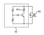
分離スイッチ素子の低耐圧化については、分離スイッチ素子への印加電圧を制限する保護回路を設けることが考えられる。分離スイッチ素子に対する保護回路として、例えば特許文献4に、図11に示すような回路が提案されている。この保護回路52は、分離スイッチ素子QSのドレイン・ソース間電圧値が所定値(設定電圧Vc)になったときに自動的に保護機能が動作し始め、分離スイッチ素子QSのドレイン・ソース間電圧を設定電圧Vcに制限するよう動作する。 In order to reduce the breakdown voltage of the separation switch element, it is conceivable to provide a protection circuit that limits the voltage applied to the separation switch element. As a protection circuit for the separation switch element, for example, Patent Document 4 proposes a circuit as shown in FIG. This
以上のような保護回路52は、分離スイッチ素子QS2のオフ期間において、分離スイッチ素子QS2のドレイン・ソース間電圧が設定電圧Vcを超える場合、保護回路52は絶えず動作し続ける。 In the
分離スイッチ素子QS2のオフ期間であっても、分離スイッチ素子QS2のドレイン・ソース間電圧がその耐圧を超えないように電圧制限することが必要のない期間(例えば、分離スイッチ素子QS2が第二の分離スイッチ素子である場合、アドレス期間や、初期化期間における下りランプ期間以外の期間等)もある。しかし、保護回路QS2は、そのような電圧制限が不要な期間においても、分離スイッチ素子QS2のドレイン・ソース間電圧を下げるように動作する。このような保護回路52の動作は保護回路QS2内の抵抗R11での電力消費を生じ、電力損失の増大を招く。 Even during the off period of the separation switch element QS2, it is not necessary to limit the voltage so that the drain-source voltage of the separation switch element QS2 does not exceed the breakdown voltage (for example, the separation switch element QS2 In the case of the separation switch element, there are an address period and a period other than the down-ramp period in the initialization period. However, the protection circuit QS2 operates so as to lower the drain-source voltage of the separation switch element QS2 even in a period in which such voltage limitation is unnecessary. Such an operation of the
本発明は上記課題を解決すべくなされたものであり、その目的とするところは、分離スイッチ素子の低耐圧化を図りつつ、分離スイッチ素子の保護回路の損失を抑制するプラズマディスプレイパネルの駆動技術を提供することにある。 The present invention has been made to solve the above-described problems, and an object of the present invention is to drive a plasma display panel that suppresses the loss of the protection circuit of the separation switch element while reducing the breakdown voltage of the separation switch element. Is to provide.
本発明の第1の態様において、維持電極と、走査電極と、アドレス電極とを備え、複数の放電セルを含むプラズマディスプレイパネルの駆動装置が提供される。そのプラズマディスプレイパネルの駆動装置は、プラズマディスプレイパネルの発光のための放電を維持する電圧を与える維持電源と、維持電源の正極への電流の流入及び/又は維持電源の負極からの電流の流出を阻止可能な分離スイッチ素子と、分離スイッチ素子と並列に接続され、分離スイッチ素子のドレイン・ソース間電圧を制限する保護回路とを備える。保護回路は、停止信号により保護回路の動作を停止させる停止手段を有する。 According to a first aspect of the present invention, there is provided a plasma display panel driving apparatus including a sustain electrode, a scan electrode, and an address electrode and including a plurality of discharge cells. The driving device of the plasma display panel includes a maintenance power source that provides a voltage for maintaining a discharge for light emission of the plasma display panel, and an inflow of current to the positive electrode of the maintenance power source and / or an outflow of current from the negative electrode of the maintenance power source. An isolation switch element that can be blocked, and a protection circuit that is connected in parallel with the isolation switch element and limits a drain-source voltage of the isolation switch element. The protection circuit has stop means for stopping the operation of the protection circuit by a stop signal.
保護回路は、所定ノードの電位または所定ノード間の電圧が所定値になったときに停止手段により停止させてもよい。 The protection circuit may be stopped by the stopping unit when the potential of the predetermined node or the voltage between the predetermined nodes reaches a predetermined value.
保護回路は、分離スイッチ素子の一端の電位を検出して、その電位が所定電位になったときに停止スイッチ素子に停止信号を出力する手段をさらに有してもよい。 The protection circuit may further include means for detecting a potential at one end of the separation switch element and outputting a stop signal to the stop switch element when the potential becomes a predetermined potential.
本発明の第2の態様において、電極間の放電による発光により画像表示可能なプラズマディスプレイパネルと、プラズマディスプレイパネルを駆動する上記のプラズマディスプレイパネルの駆動装置とを備える、プラズマディスプレイが提供される。 In a second aspect of the present invention, there is provided a plasma display comprising a plasma display panel capable of displaying an image by light emission by discharge between electrodes, and the plasma display panel driving apparatus for driving the plasma display panel.
本発明によれば、分離スイッチ素子に対して設けた保護回路を強制的に停止させることができ、これにより、保護回路の作動が必要のない期間における保護回路での電力損失を低減することができる。 According to the present invention, the protection circuit provided for the separation switch element can be forcibly stopped, thereby reducing power loss in the protection circuit during a period when the protection circuit is not required to operate. it can.
また、停止させる機能を有する保護回路は設定電圧を低くすることが可能となるので、分離スイッチ素子の低耐圧化が図れるため、実装時における分離スイッチ素子の並列接続数を低減でき、回路規模を削減できる。さらに、実装面積が小さくなることで、基板による配線インピーダンスを低減でき、PDPへの電圧印加時に発生する高周波数成分であるリンギングを低減でき、PDPの動作マージンが拡大する。さらに、放電維持期間での分離スイッチ素子による導通損失が大きく削減されるので、消費電力を低減できる。 In addition, since the protection circuit having the function of stopping can reduce the set voltage, the isolation switch element can be reduced in withstand voltage, so the number of parallel connection of the isolation switch element during mounting can be reduced, and the circuit scale can be reduced. Can be reduced. Furthermore, since the mounting area is reduced, the wiring impedance due to the substrate can be reduced, ringing, which is a high frequency component generated when a voltage is applied to the PDP, can be reduced, and the operation margin of the PDP is expanded. Furthermore, since the conduction loss due to the separation switch element during the discharge sustain period is greatly reduced, power consumption can be reduced.
以下、添付の図面を参照しつつ本発明の実施形態について説明する。 Hereinafter, embodiments of the present invention will be described with reference to the accompanying drawings.
実施の形態1
1.1 構成
1.1.1 プラズマディスプレイ
図1は本発明の実施の形態によるプラズマディスプレイの構成を示すブロック図である。プラズマディスプレイは、PDP駆動装置10、プラズマディスプレイパネル(PDP)20、及び制御部30を有する。
1.1 Configuration 1.1.1 Plasma Display FIG. 1 is a block diagram showing a configuration of a plasma display according to an embodiment of the present invention. The plasma display includes a
1.1.2 プラズマディスプレイパネル
PDP20は例えばAC型であり、三電極面放電型構造を有する。PDP20の背面基板上にはアドレス電極A1、A2、A3、…がパネルの幅方向に沿って配置される。PDP20の前面基板上には維持電極X1、X2、X3、…と走査電極Y1、Y2、Y3、…とが交互に、かつパネルの長手方向に沿って配置される。維持電極X1、X2、X3、…は互いに接続され、電位が実質的に等しい。アドレス電極A1、A2、A3、…と、走査電極Y1、Y2、Y3、…とは、一本ずつ個別に電位を変化させ得る。1.1.2 Plasma Display Panel The
互いに隣り合う維持電極と走査電極との対(例えば維持電極X2と走査電極Y2との対)及びアドレス電極(例えばアドレス電極A2)の交差点には放電セルが設置される(例えば、図1に示される斜線部P部分参照)。放電セルの表面には、誘電体から成る層(誘電体層)、電極と誘電体層とを保護するための層(保護層)、及び蛍光物質を含む層(蛍光層)が設けられる。放電セルの内部にはガスが封入される。維持電極、走査電極、及びアドレス電極の間に対し所定のパルス電圧が印加されると、放電セルで放電が生じる。そのとき、放電セル中のガス分子が電離し、紫外線を発する。その紫外線が放電セル表面の蛍光物質を励起し、蛍光を発生させる。このようにして放電セルが発光する。 A discharge cell is installed at the intersection of a pair of sustain electrode and scan electrode (for example, a pair of sustain electrode X2 and scan electrode Y2) and an address electrode (for example, address electrode A2) adjacent to each other (for example, shown in FIG. 1). (See the shaded part P). On the surface of the discharge cell, a layer made of a dielectric (dielectric layer), a layer for protecting the electrode and the dielectric layer (protective layer), and a layer containing a fluorescent substance (fluorescent layer) are provided. Gas is sealed inside the discharge cell. When a predetermined pulse voltage is applied between the sustain electrode, the scan electrode, and the address electrode, a discharge is generated in the discharge cell. At that time, gas molecules in the discharge cell are ionized and emit ultraviolet rays. The ultraviolet rays excite the fluorescent material on the surface of the discharge cell to generate fluorescence. In this way, the discharge cell emits light.
1.1.3 PDP駆動装置
PDP駆動装置10は、走査電極駆動部11、維持電極駆動部12、及びアドレス電極駆動部13を含む。1.1.3 PDP Drive Device The
走査電極駆動部11と維持電極駆動部12の入力端子1は、電源部(図示せず)に接続される。電源部はまず、外部の商用交流電源からの交流電圧を一定の直流電圧(例えば400V)に変換する。更に、その直流電圧をDC−DCコンバータにより、所定の直流電圧Vsへ変換する。その直流電圧VsはPDP駆動装置10に印加される。これにより、入力端子1の電位は、接地電位(≒0)に対して直流電圧Vsだけ高く維持される。
走査電極駆動部11の出力端子はPDP20の走査電極Y1、Y2、Y3、…のそれぞれに個別に接続される。走査電極駆動部11は走査電極Y1、Y2、Y3、…のそれぞれの電位を個別に変化させる。 The output terminals of the scan
維持電極駆動部12の出力端子はPDP20の維持電極X1、X2、X3、…に接続される。維持電極駆動部12は維持電極X1、X2、X3、…の電位を一様に変化させる。 The output terminal of the sustain
アドレス電極駆動部13はPDP20のアドレス電極A1、A2、A3、…のそれぞれに個別に接続される。アドレス電極駆動部13は、外部からの映像信号に基づき信号パルス電圧を発生させ、アドレス電極A1、A2、A3、…の中から選択された電極に対し印加する。 The
PDP駆動装置10はADS(Address Display-period Separation)方式に従い、PDP20の各電極の電位を制御する。ADS方式はサブフィールド方式の一種である。例えば日本のテレビ放送では画像が一フィールドずつ、1/60秒(=約16。7msec)間隔で送られる。それにより、一フィールド当たりの表示時間が一定である。サブフィールド方式ではフィールドがそれぞれ複数のサブフィールドに分けられる。ADS方式では更に、サブフィールドごとに、PDP20の全ての放電セルに対し三つの期間(初期化期間、アドレス期間、及び放電維持期間)が共通に設定される。放電維持期間の長さはサブフィールドごとに異なる。初期化期間、アドレス期間、及び放電維持期間のそれぞれでは、異なるパルス電圧が次のように、放電セルに対し印加される。 The
初期化期間では、初期化パルス電圧が維持電極X1、X2、X3、…と走査電極Y1、Y2、Y3、…との間に印加される。それにより、全ての放電セルで壁電荷が均一化される。 In the initialization period, an initialization pulse voltage is applied between the sustain electrodes X1, X2, X3,... And the scan electrodes Y1, Y2, Y3,. Thereby, wall charges are made uniform in all the discharge cells.
アドレス期間では、走査電極駆動部11が走査パルス電圧を走査電極Y1、Y2、Y3、…に対し、順次印加する。走査パルス電圧の印加と同時に、アドレス電極駆動部13が信号パルス電圧を、アドレス電極A1、A2、A3、…に対し印加する。ここで、信号パルス電圧が印加されるべきアドレス電極は、外部から入力される映像信号に基づき選択される。走査パルス電圧が走査電極の一つに印加され、かつ信号パルス電圧がアドレス電極の一つに印加されるとき、その走査電極とアドレス電極との交差点に位置する放電セルで放電が生じる。その放電により、その放電セル表面に新たな壁電荷が蓄積される。 In the address period, the
放電維持期間では、走査電極駆動部11と維持電極駆動部12とが交互に、放電維持パルス電圧をそれぞれ、走査電極Y1、Y2、Y3、…と維持電極X1、X2、X3、…とに対し印加する。そのとき、アドレス期間中に壁電荷が蓄積された放電セルでは放電が維持されるので、発光が生じる。放電維持期間の長さはサブフィールドごとに異なるので、放電セルの一フィールド当たりの発光時間、すなわち放電セルの輝度は、発光すべきサブフィールドの選択により調整される。 In the discharge sustain period, the scan
走査電極駆動部11、維持電極駆動部12、及びアドレス電極駆動部13はそれぞれ、内部にスイッチングインバータを含む。制御部30は、それらの駆動部についてスイッチング制御を行う。それにより、初期化パルス電圧、走査パルス電圧、信号パルス電圧、及び放電維持パルス電圧がそれぞれ、所定の波形及びタイミングで発生する。制御部30は特に、外部からの映像信号に基づき、信号パルス電圧の印加先のアドレス電極を選択する。制御部30は更に、その信号パルス電圧の印加後の放電維持期間の長さ、すなわちその信号パルス電圧を印加すべきサブフィールドを決定する。その結果、それぞれの放電セルが適切な輝度で発光する。こうして、PDP20には映像信号に対応する映像が再現される。 Scan
1.1.3.1 走査電極駆動部
図2に、走査電極駆動部11の詳細な構成を示す。図2にはPDP20の等価回路も合わせて示している。走査電極駆動部11は、走査パルス発生部1Y、初期化パルス発生部2Y及び放電維持パルス発生部3Y、回収回路部4Yを含む。PDP20は、維持電極Xと走査電極Yとの間の浮遊容量Cp(以下「PDPのパネル容量」という)により等価的に表されており、放電セルでの放電時にPDP20を流れる電流の経路は省略される。図2において、維持電極Xに接続する維持電極駆動部は省略しており、図中、維持電極Xは接地状態で表されている。1.1.3.1 Scan Electrode Drive Unit FIG. 2 shows a detailed configuration of the scan
(走査パルス発生部)
走査パルス発生部1Yは、第一の定電圧源V1と、ハイサイド走査スイッチ素子Q1Y及びローサイド走査スイッチ素子Q2Yの直列回路とを含む。(Scanning pulse generator)
The
第一の定電圧源V1は、例えばDC−DCコンバータ(図示せず)により、電源部から印加される直流電圧Vs(=維持電源Vs)に基づき、正極の電位を負極の電位より一定の電圧V1だけ高く維持する。 The first constant voltage source V1 is, for example, a DC-DC converter (not shown) based on a direct current voltage Vs (= maintenance power supply Vs) applied from a power supply unit, the positive electrode potential being a constant voltage from the negative electrode potential. Keep V1 higher.
二つの走査スイッチ素子Q1Y、Q2Yは例えばMOSFETである。その他にIGBT又はバイポーラトランジスタであっても良い。 The two scanning switch elements Q1Y and Q2Y are, for example, MOSFETs. In addition, an IGBT or a bipolar transistor may be used.
第一の定電圧源V1の正極はハイサイド走査スイッチ素子Q1Yのドレインに接続される。ハイサイド走査スイッチ素子Q1Yのソースはローサイド走査スイッチ素子Q2Yのドレインに接続される。それらの間の接続点J1YはPDP20の一つの走査電極Yに接続される。ローサイド走査スイッチ素子Q2Yのソースは、第一の定電圧源V1の負極に接続される。 The positive electrode of the first constant voltage source V1 is connected to the drain of the high side scan switch element Q1Y. The source of the high side scan switch element Q1Y is connected to the drain of the low side scan switch element Q2Y. A connection point J1Y between them is connected to one scan electrode Y of the
ここで、ハイサイド走査スイッチ素子Q1Yとローサイド走査スイッチ素子Q2Yの直列接続回路(図2に示す破線で囲まれた部分)は、実際には、走査電極Y1、Y2、…と同数だけ設けられ、走査電極Y1、Y2、…のそれぞれに一つずつ接続される。 Here, the series connection circuit of the high-side scan switch element Q1Y and the low-side scan switch element Q2Y (portion surrounded by a broken line shown in FIG. 2) is actually provided in the same number as the scan electrodes Y1, Y2,. One is connected to each of the scanning electrodes Y1, Y2,.
(初期化パルス発生部)
初期化パルス発生部2Yは、第二の定電圧源V2、ハイサイドランプ波形発生部QR1、ローサイドランプ波形発生部QR2、アドレススイッチ素子Q3Y、第三の定電圧源V3、第一の分離スイッチ素子QS1、第二の分離スイッチ素子QS2、及び保護回路50を含む。(Initialization pulse generator)
The
第二の定電圧源V2は、例えばDC−DCコンバータにより、維持電源Vsに基づき、その正極の電位を負極の電位より所定電圧V2だけ高く維持する。 The second constant voltage source V2 maintains the positive electrode potential higher than the negative electrode potential by a predetermined voltage V2 based on the maintenance power source Vs, for example, by a DC-DC converter.
第三の定電圧源V3は、例えばDC−DCコンバータにより、維持電源Vsに基づき、その正極の電位を負極の電位より所定電圧V3だけ高く維持する。 The third constant voltage source V3 maintains the positive electrode potential higher than the negative electrode potential by a predetermined voltage V3 based on the maintenance power source Vs by, for example, a DC-DC converter.
ランプ波形発生部QR1、QR2は例えばNチャネルMOSFET(NMOS)と、そのNMOSのゲートとドレインとを接続するコンデンサとで構成される。ランプ波形発生部QR1、QR2がオンするとき、ドレイン・ソース間電圧が実質的に一定の速度で零まで変化する。 The ramp waveform generators QR1 and QR2 are composed of, for example, an N-channel MOSFET (NMOS) and a capacitor that connects the gate and drain of the NMOS. When the ramp waveform generators QR1 and QR2 are turned on, the drain-source voltage changes to zero at a substantially constant speed.
第三の定電圧源V3の正極は接地され、第三の定電圧源V3の負極はアドレススイッチ素子Q3Yのソースに接続される。アドレススイッチ素子Q3Yのドレインは第一の定電圧源V1の負極に接続される。ローサイドランプ波形発生部QR2のソースは第三の定電圧源V3の負極に接続され、ローサイドランプ波形発生部QR2のドレインは第一の定電圧源V1の負極に接続される。 The positive electrode of the third constant voltage source V3 is grounded, and the negative electrode of the third constant voltage source V3 is connected to the source of the address switch element Q3Y. The drain of the address switch element Q3Y is connected to the negative electrode of the first constant voltage source V1. The source of the low side ramp waveform generator QR2 is connected to the negative electrode of the third constant voltage source V3, and the drain of the low side ramp waveform generator QR2 is connected to the negative electrode of the first constant voltage source V1.
第二の分離スイッチ素子QS2のソースは第一の定電圧源V1の負極に接続され、第二の分離スイッチ素子QS2のドレインは、第一の分離スイッチ素子QS1のドレインに接続される。第一の分離スイッチ素子QS1のソースは第二の定電圧源V2の負極に接続される。第二の定電圧源V2の正極はハイサイドランプ波形発生部QR1のドレインに接続される。ハイサイドランプ波形発生部QR1のソースは第一の分離スイッチ素子QS1のドレインに接続される。保護回路50の一端は第二の分離スイッチ素子QS2のドレインに接続され、その他端は第二の分離スイッチ素子QS2のソースに接続される。 The source of the second separation switch element QS2 is connected to the negative electrode of the first constant voltage source V1, and the drain of the second separation switch element QS2 is connected to the drain of the first separation switch element QS1. The source of the first separation switch element QS1 is connected to the negative electrode of the second constant voltage source V2. The positive electrode of the second constant voltage source V2 is connected to the drain of the high side ramp waveform generator QR1. The source of the high side ramp waveform generator QR1 is connected to the drain of the first separation switch element QS1. One end of the
保護回路50は第二の分離スイッチ素子QS2と並列に接続され、第二の分離スイッチ素子QS2のドレイン・ソース間電圧を一定電圧内に制限する。また、保護回路50は外部からの停止信号により強制的にその動作を停止させる機能を有する。保護回路50の詳細は後述する。 The
(放電維持パルス発生部)
放電維持パルス発生部3Yは、ハイサイド維持スイッチ素子Q7Yとローサイド維持スイッチ素子Q8Yの直列回路と、維持放電期間中に走査電極Yに維持電圧を供給する維持電源Vsとを含む。(Discharge sustain pulse generator)
Discharge sustain
維持電源Vsは、正極の電位を負極の電位より一定の電圧Vsだけ高く維持する。維持電源Vsの正極はハイサイド維持スイッチ素子Q7Yのドレインに接続され、ハイサイド維持スイッチ素子Q7Yのソースはローサイド維持スイッチ素子Q8Yのドレインに接続される。ローサイド維持スイッチ素子Q8Yのソースは維持電源Vsの負極に接続される。維持電源Vsの負極は例えば0V(接地状態)である。ハイサイド維持スイッチ素子Q7Yとローサイド維持スイッチ素子Q8Yとの間の接続点J2Yは、放電維持パルス発生部3Yの出力端子として、第一の分離スイッチ素子QS1のソースに接続される。 The maintenance power source Vs maintains the positive electrode potential higher than the negative electrode potential by a certain voltage Vs. The positive electrode of sustain power supply Vs is connected to the drain of high side sustain switch element Q7Y, and the source of high side sustain switch element Q7Y is connected to the drain of low side sustain switch element Q8Y. The source of the low-side sustain switch element Q8Y is connected to the negative electrode of the sustain power supply Vs. The negative electrode of the maintenance power source Vs is, for example, 0V (ground state). A connection point J2Y between the high-side sustain switch element Q7Y and the low-side sustain switch element Q8Y is connected to the source of the first separation switch element QS1 as the output terminal of the discharge sustain
(回収回路)
回収回路4Yは、第一の回収インダクタLY1、第二の回収インダクタLY2、回収コンデンサCY、第一の回収ダイオードD1、第二の回収ダイオードD2、ハイサイド回収スイッチ素子Q9Y、及びローサイド回収スイッチ素子Q10Yを含む。二つの回収スイッチ素子Q9Y、Q10Yは例えばMOSFETである。その他にIGBT又はバイポーラトランジスタであっても良い。(Recovery circuit)
The
ハイサイド回収スイッチ素子Q9Yのソースは第一の回収ダイオードD1のアノードと接続し、第一の回収ダイオードD1のカソードは第一の回収インダクタLY1の一端に接続する。第二の回収インダクタLY2の一端は、第二の回収ダイオードD2のアノードと接続し、第二の回収ダイオードD2のカソードは、ローサイド回収スイッチ素子Q10Yのドレインと接続する。第一の回収インダクタLY1の他端は接続点J2Yに接続される。第二の回収インダクタLY2の他端は接続点J2Yに接続される。回収コンデンサCYの一端は維持電源Vsの負極に接続され、回収コンデンサCYの他端はハイサイド回収スイッチ素子Q9Yのドレイン及びローサイド回収スイッチ素子Q10Yのソースに接続される。 The source of the high side recovery switch element Q9Y is connected to the anode of the first recovery diode D1, and the cathode of the first recovery diode D1 is connected to one end of the first recovery inductor LY1. One end of the second recovery inductor LY2 is connected to the anode of the second recovery diode D2, and the cathode of the second recovery diode D2 is connected to the drain of the low-side recovery switch element Q10Y. The other end of the first recovery inductor LY1 is connected to the connection point J2Y. The other end of the second recovery inductor LY2 is connected to the connection point J2Y. One end of the recovery capacitor CY is connected to the negative electrode of the maintenance power supply Vs, and the other end of the recovery capacitor CY is connected to the drain of the high side recovery switch element Q9Y and the source of the low side recovery switch element Q10Y.
回収コンデンサCYの容量はPDP20のパネル容量Cpより十分に大きい。回収コンデンサCYの両端電圧は、電源部から印加される維持電圧Vsの半値Vs/2と実質的に等しく維持される。 The capacity of the recovery capacitor CY is sufficiently larger than the panel capacity Cp of the
1.2 動作
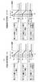
図3は、初期化期間、アドレス期間及び放電維持期間それぞれでの、PDP20の走査電極Yに対する印加電圧波形、並びに走査電極駆動部11に含まれる各スイッチ素子のオン期間を示す図である。図3では、それぞれのスイッチ素子のオン期間が斜線部で示される。以下、各期間の動作について説明する。なお、各素子の電極やノードの電圧、電位の値は接地電位(=0)を基準とする。1.2 Operation FIG. 3 is a diagram showing a voltage waveform applied to the scan electrode Y of the
1.2.1 初期化期間
初期化期間は初期化パルス電圧の変化に応じて次の8つのモードI〜VIIIに分けられる。1.2.1 Initialization Period The initialization period is divided into the following eight modes I to VIII according to changes in the initialization pulse voltage.
<モードI>
走査電極駆動部11では、ローサイド走査スイッチ素子Q2Y、第一の分離スイッチ素子QS1、第二の分離スイッチ素子QS2及びハイサイド維持スイッチ素子Q7Yがオン状態に維持される。残りのスイッチ素子はオフ状態に維持される。それにより、走査電極Yは接地電位(≒0)から維持電圧Vsだけ高い電位に維持される。<Mode I>
In
<モードII>
走査電極駆動部11では、ローサイド走査スイッチ素子Q2Y及び第一の分離スイッチ素子QS1がオン状態に維持されたまま、ハイサイド維持スイッチ素子Q7Y及び第二の分離スイッチ素子QS2がオフし、ローサイドランプ波形発生部QR2がオンする。残りのスイッチ素子はオフ状態に維持される。走査電極Yの電位は一定の速度で、接地電位(≒0)を基準として、第三の定電圧源の電圧V3から切替電圧V4だけ高い電位(-V3+V4)まで下降する。こうして、PDP20の全ての放電セルに対して一様に、印加電圧が、(-V3+V4)の電位まで比較的緩やかに下降する。それにより、PDP20の全ての放電セルで壁電荷が一様に除去され、均一化される。そのとき、印加電圧の下降速度が小さいので、放電セルの発光は微弱に抑えられる。<Mode II>
In the scan
<モードIII>
走査電極駆動部11では、ローサイドランプ波形発生部QR2と第一の分離スイッチ素子QS1がオン状態に維持されたまま、ローサイド走査スイッチ素子Q2Yがオフし、ハイサイド走査スイッチ素子Q1Yがオンする。残りのスイッチ素子はオフ状態に維持される。<Mode III>
In the scan
ハイサイド走査スイッチ素子Q1Yのドレインは、(-V3+V4)から電圧V1だけ高い電位(-V3+V4+V1)に変化し、ローサイド走査スイッチ素子Q2Yのソースは(-V3+V4)となる。その後、ローサイドランプ波形発生部QR2の動作によって、ローサイド走査スイッチ素子Q2Yのソースの電位は徐々に低下し、電圧V3だけ低い電位-V3に維持される。このときハイサイド走査スイッチ素子Q1Yのドレインもローサイド走査スイッチ素子Q2Yのソースの変化によって低下し、ハイサイド走査スイッチ素子Q1Yのドレインは、電位-V3から電圧V1だけ高い電位Vp(以下「走査パルス電圧の上限」という。)に維持される。 The drain of the high-side scan switch element Q1Y changes from (-V3 + V4) to a potential (-V3 + V4 + V1) that is higher by the voltage V1, and the source of the low-side scan switch element Q2Y becomes (-V3 + V4) . Thereafter, the operation of the low-side ramp waveform generator QR2 gradually decreases the source potential of the low-side scan switch element Q2Y, and is maintained at the potential −V3 that is lower by the voltage V3. At this time, the drain of the high-side scan switch element Q1Y also decreases due to the change in the source of the low-side scan switch element Q2Y, and the drain of the high-side scan switch element Q1Y has a potential Vp (hereinafter referred to as “scanning pulse voltage”) The upper limit of “.” Is maintained.
この期間は全ての走査電極Yについて、ハイサイド走査スイッチ素子Q1Yがオン状態に維持され、ローサイド走査スイッチ素子Q2Yがオフ状態に維持される。それにより、全ての走査電極Yの電位が一様に走査パルス電圧の上限Vpに維持されるので放電セルは放電には至らず、壁電荷が保持される。例えば、1フィールド中のサブフィールド数や維持パルス数が少ない画像の場合、通常の動作期間で初期化、アドレス、維持動作を行うと時間が余ってしまう。そこで、時間を調整するために、この期間の時間を長くしている。本期間は画像によって長くなったり短くなったりする。 During this period, for all the scan electrodes Y, the high side scan switch element Q1Y is maintained in the on state and the low side scan switch element Q2Y is maintained in the off state. As a result, the potentials of all the scan electrodes Y are uniformly maintained at the upper limit Vp of the scan pulse voltage, so that the discharge cells do not reach the discharge and the wall charges are held. For example, in the case of an image with a small number of subfields and sustain pulses in one field, time is left if initialization, address, and sustain operations are performed during a normal operation period. Therefore, in order to adjust the time, the time of this period is increased. This period becomes longer or shorter depending on the image.
<モードIV>
走査電極駆動部11では、第一の分離スイッチ素子QS1がオン状態に維持されたまま、ハイサイド走査スイッチ素子Q1Y、ローサイドランプ波形発生部QR2がオフし、ローサイド走査スイッチ素子Q2Y、第二の分離スイッチ素子QS2及びローサイド維持スイッチ素子Q8Yをオンし、残りのスイッチ素子はオフ状態に維持される。それにより、走査電極Yの電位は接地電位(≒0)に下降する。<Mode IV>
In the scan
<モードV>
走査電極駆動部11では、ローサイド走査スイッチ素子Q2Y、第一の分離スイッチ素子QS1、第二の分離スイッチ素子QS2がオン状態に維持されたまま、ローサイド維持スイッチ素子Q8Yをオフし、ハイサイド維持スイッチ素子Q7Yをオン状態に維持される。それにより、走査電極Yの電位が接地電位(≒0)から維持電圧Vsだけ高い電位まで上昇する。<Mode V>
In the
<モードVI>
走査電極駆動部11では、ローサイド走査スイッチ素子Q2Y、ハイサイド維持スイッチ素子Q7Y及び第二の分離スイッチ素子QS2がオン状態に維持されたまま、第一の分離スイッチ素子QS1がオフし、ハイサイドランプ波形発生部QR1がオンする。残りのスイッチ素子はオフ状態に維持される。それにより、走査電極Yの電位が一定の速度で、電位Vsから電位Vr(=Vs+V2、以下「初期化パルス電圧の上限」という。)まで上昇する。<Mode VI>
In the scan
こうして、PDP20の全ての放電セルに対して一様に、印加電圧が、初期化パルス電圧の上限Vrに向かって比較的緩やかに上昇する。それにより、PDP20の全ての放電セルで一様な壁電荷が蓄積される。そのとき、印加電圧の上昇速度が小さいので、放電セルの発光は微弱に抑えられる。 In this way, the applied voltage uniformly increases for all discharge cells of the
<モードVII>
走査電極駆動部11では、ローサイド走査スイッチ素子Q2Y、第二の分離スイッチ素子QS2及びハイサイド維持スイッチ素子Q7Yがオン状態に維持されたまま、ハイサイドランプ発生部QR1がオフし、第一の分離スイッチ素子QS1がオンする。残りのスイッチ素子はオフ状態に維持される。それにより、走査電極Yの電位が電位Vsに維持される。<Mode VII>
In the
<モードVIII>
走査電極駆動部11では、ローサイド走査スイッチ素子Q2Y及び第一の分離スイッチ素子QS1がオン状態に維持されたまま、ハイサイド維持スイッチ素子Q7Y及び第二の分離スイッチ素子QS2がオフし、ローサイドランプ波形発生部QR2がオンする。残りのスイッチ素子はオフ状態に維持される。走査電極Yの電位は一定の速度で、電位(-V3+V4)まで下降する。こうして、PDP20の全ての放電セルに対して一様に、モードIVでの印加電圧とは逆極性の比較的緩やかな電圧が印加されるので、全ての放電セルで壁電荷が一様に除去され、均一化される。そのとき印加電圧の下降速度が小さいので、放電セルの発光は微弱に抑えられる。<Mode VIII>
In the scan
1.2.2 アドレス期間
アドレス期間中、走査電極駆動部11では、第一の分離スイッチ素子QS1がオン状態に維持されたまま、ローサイド走査スイッチ素子Q2Y、ローサイドランプ波形発生部QR2がオフし、ハイサイド走査スイッチ素子Q1Y、アドレススイッチ素子Q3Y、ローサイド維持スイッチ素子Q8Yがオンする。これによって、ハイサイド走査スイッチ素子Q1Yのドレイン電位は、電位Vp(走査パルス電圧の上限)に維持され、ローサイド走査スイッチ素子Q2Yのソース電位は(-V3)に維持される。1.2.2 Address Period During the address period, in the
アドレス期間の開始時、全ての走査電極Yについて、ハイサイド走査スイッチ素子Q1Yがオン状態に維持され、ローサイド走査スイッチ素子Q2Yがオフ状態に維持される。それにより、全ての走査電極Yの電位が一様に走査パルス電圧の上限Vpに維持される。 At the start of the address period, for all scan electrodes Y, the high side scan switch element Q1Y is maintained in the on state and the low side scan switch element Q2Y is maintained in the off state. As a result, the potentials of all the scan electrodes Y are uniformly maintained at the upper limit Vp of the scan pulse voltage.
走査電極駆動部11は続いて、走査電極Yの電位を次のように変化させる(図3における走査パルス電圧SP参照)。一つの走査電極Yが選択されると、その走査電極Yに接続されるハイサイド走査スイッチ素子Q1Yがオフし、ローサイド走査スイッチ素子Q2Yがオンする。それにより、その走査電極Yの電位が-V3まで下降する。その走査電極Yの電位が所定時間、-V3に維持されると、その走査電極Yに接続されるローサイド走査スイッチ素子Q2Yがオフし、ハイサイド走査スイッチ素子Q1Yがオンする。それにより、その走査電極Yの電位が走査パルス電圧の上限Vpまで上昇する。走査電極駆動部11は走査電極のそれぞれに接続される走査スイッチ素子対Q1Y、Q2Yについて、上記と同様なスイッチング動作を順次行う。こうして、走査パルス電圧SPが走査電極のそれぞれに対し順次、印加される。 Subsequently, the
アドレス期間中、外部から入力される映像信号に基づき一つのアドレス電極Aが選択されると、その選択されたアドレス電極Aの電位が所定時間、信号パルス電圧の上限Vaまで上昇する(図示せず)。 When one address electrode A is selected based on a video signal input from the outside during the address period, the potential of the selected address electrode A rises to the upper limit Va of the signal pulse voltage for a predetermined time (not shown). ).
例えば、走査パルス電圧SPが一つの走査電極Yに印加され、かつ信号パルス電圧が一つのアドレス電極Aに印加されるとき、その走査電極Yとアドレス電極Aとの間の電圧は他の電極間の電圧より高い。従って、その走査電極Yとアドレス電極Aとの間の交差点に位置する放電セルでは放電が生じる。その放電により、その放電セル表面に新たな壁電荷が蓄積される。 For example, when the scan pulse voltage SP is applied to one scan electrode Y and the signal pulse voltage is applied to one address electrode A, the voltage between the scan electrode Y and the address electrode A is between the other electrodes. Higher than the voltage of. Therefore, discharge occurs in the discharge cell located at the intersection between the scan electrode Y and the address electrode A. Due to the discharge, new wall charges are accumulated on the surface of the discharge cell.
その後、放電維持期間において、走査電極駆動部11と維持電極駆動部12とが交互に、放電維持パルス電圧をそれぞれ、走査電極Yと維持電極Xとに対し印加する(図3参照)。そのとき、アドレス期間中に壁電荷が蓄積された放電セルでは放電が維持されるので、発光が生じる。 Thereafter, in the sustain period, scan
1.2.3 放電維持期間
放電維持期間について説明する。ローサイド走査スイッチ素子Q2Y、第一の分離スイッチ素子QS1及び第二の分離スイッチ素子QS2は常にオン状態に維持される。1.2.3 Discharge sustain period The discharge sustain period will be described. The low-side scanning switch element Q2Y, the first separation switch element QS1, and the second separation switch element QS2 are always maintained in the on state.
ハイサイド回収スイッチ素子Q9Yがオンする直前には、ローサイド維持スイッチ素子Q8Yがオンしており、パネル容量Cpの両端電圧は0Vに維持される。ハイサイド回収スイッチ素子Q9Yがオンすると、回収コンデンサCYと、ハイサイド回収スイッチ素子Q9Yと、第一の回収ダイオードD1と、第一の回収インダクタLY1と、パネル容量Cpとにより、LC共振回路が形成される。これにより、パネル容量Cpの両端電圧はVsまで増加する。残りのスイッチ素子はオフ状態に維持される。 Immediately before the high-side recovery switch element Q9Y is turned on, the low-side sustain switch element Q8Y is turned on, and the voltage across the panel capacitance Cp is maintained at 0V. When the high-side recovery switch element Q9Y is turned on, an LC resonance circuit is formed by the recovery capacitor CY, the high-side recovery switch element Q9Y, the first recovery diode D1, the first recovery inductor LY1, and the panel capacitance Cp. Is done. As a result, the voltage across the panel capacitance Cp increases to Vs. The remaining switch elements are kept off.
次に、ハイサイド回収スイッチ素子Q9Yがオフして、ハイサイド維持スイッチ素子Q7Yがオンすれば、パネル容量Cpの両端電圧はVsに維持される。このとき、ハイサイド維持スイッチ素子Q7Yのドレイン・ソース間電圧は零であるので、ほぼ損失なくオンすることができる(残りのスイッチ素子はオフ状態に維持される)。 Next, when the high side recovery switch element Q9Y is turned off and the high side sustain switch element Q7Y is turned on, the voltage across the panel capacitance Cp is maintained at Vs. At this time, since the drain-source voltage of the high side sustain switch element Q7Y is zero, it can be turned on with almost no loss (the remaining switch elements are maintained in the off state).
所定時間経過後、ハイサイド維持スイッチ素子Q7Yがオフして、ローサイド回収スイッチ素子Q10Yがオンすると(残りのスイッチ素子はオフ状態に維持される)、回収コンデンサCYと、ローサイド回収スイッチ素子Q10Yと、第二の回収ダイオードD2と、第二の回収インダクタLY2と、パネル容量Cpとにより、LC共振回路が形成される。これにより、パネル容量Cpの両端電圧は0まで減少する。 After a predetermined time has elapsed, when the high side sustain switch element Q7Y is turned off and the low side recovery switch element Q10Y is turned on (the remaining switch elements are maintained in the off state), the recovery capacitor CY, the low side recovery switch element Q10Y, An LC resonance circuit is formed by the second recovery diode D2, the second recovery inductor LY2, and the panel capacitance Cp. As a result, the voltage across the panel capacitance Cp decreases to zero.
次に、ローサイド回収スイッチ素子Q10Yがオフして、ローサイド維持スイッチ素子Q8Yがオンすれば、パネル容量Cpの両端電圧は0に維持される。このとき、ローサイド維持スイッチ素子Q8Yのドレイン・ソース間電圧は零であるので、ほぼ損失なくオンすることができる(残りのスイッチ素子はオフ状態に維持される)。 Next, when the low-side recovery switch element Q10Y is turned off and the low-side sustain switch element Q8Y is turned on, the voltage across the panel capacitance Cp is maintained at 0. At this time, since the drain-source voltage of the low-side sustain switch element Q8Y is zero, it can be turned on with almost no loss (the remaining switch elements are maintained in the off state).
走査電極Yの電位が上下するとき、回収コンデンサCYとパネル容量Cpとの間で電力が効率良く交換される。こうして、放電維持パルス電圧の印加時、パネル容量の充放電に起因する無効電力が低減する。 When the potential of the scan electrode Y rises and falls, power is efficiently exchanged between the recovery capacitor CY and the panel capacitance Cp. Thus, the reactive power due to charging / discharging of the panel capacitance is reduced when the sustaining voltage pulse is applied.
1.2.4 保護回路の動作
図4(a)に保護回路50の詳細な構成を示す。保護回路50は、保護用スイッチ素子S1、第一の制限抵抗R1、ゲート用ツェナーダイオードZD1、第一の検出抵抗R2、第二の検出抵抗R3、及び停止スイッチ素子S2を含む。1.2.4 Operation of Protection Circuit FIG. 4A shows a detailed configuration of the
保護用スイッチ素子S1のコレクタは第一の制限抵抗R1の一端と接続し、保護用スイッチ素子S1のベースはゲート用ツェナーダイオードZD1のアノードと接続し、保護用スイッチ素子S1のエミッタは第二の分離スイッチ素子QS2のソースと接続する。第一の制限抵抗R1の他端は第二の分離スイッチ素子QS2のドレインと接続する。第一の検出抵抗R2と第二の検出抵抗R3は直列接続し、その接続点はゲート用ツェナーダイオードZD1のカソードと接続し、第一の検出抵抗R2は第二の分離スイッチ素子QS2のドレインと接続し、第二の検出抵抗R3は第二の分離スイッチ素子QS2のソースと接続する。 The collector of the protective switch element S1 is connected to one end of the first limiting resistor R1, the base of the protective switch element S1 is connected to the anode of the gate Zener diode ZD1, and the emitter of the protective switch element S1 is the second Connect to the source of separation switch element QS2. The other end of the first limiting resistor R1 is connected to the drain of the second separation switch element QS2. The first detection resistor R2 and the second detection resistor R3 are connected in series, the connection point is connected to the cathode of the gate Zener diode ZD1, and the first detection resistor R2 is connected to the drain of the second separation switch element QS2. The second detection resistor R3 is connected to the source of the second separation switch element QS2.
停止スイッチ素子S2のドレインはツェナーダイオードZD1のカソードに接続され、停止スイッチ素子S2のソースは第二の分離スイッチ素子QS2のソースに接続される。停止スイッチ素子S2のゲートには、停止スイッチ素子S2をオン/オフさせるための制御信号(作動信号/停止信号)が印加される。例えば、停止信号としてアドレス期間を示す信号を入力し、アドレス期間中、停止スイッチ素子S2をオンさせることで、保護回路50の動作を強制的に停止させることを可能とする。 The drain of the stop switch element S2 is connected to the cathode of the Zener diode ZD1, and the source of the stop switch element S2 is connected to the source of the second separation switch element QS2. A control signal (operation signal / stop signal) for turning on / off the stop switch element S2 is applied to the gate of the stop switch element S2. For example, by inputting a signal indicating the address period as a stop signal and turning on the stop switch element S2 during the address period, the operation of the
保護回路50は、第二の分離スイッチ素子QS2がオフしている期間において、停止信号が印加されていない場合に動作する。保護回路50は、第二の分離スイッチ素子QS2のドレイン・ソース間電圧を設定電圧Vcに制限する機能を有する。 The
第二の分離スイッチ素子QS2のドレイン・ソース間電圧の上昇に伴い、第二の検出抵抗R3の両端電圧が上昇する。第二の分離スイッチ素子QS2のドレイン・ソース間電圧が設定電圧Vcに達すると、第二の検出抵抗R3の両端電圧が所定電圧(第一の検出抵抗R2と第二の検出抵抗R3の抵抗値の比で決まる値)に達する。このとき、保護用スイッチ素子S1のベース・エミッタ間電圧はゲート用ツェナーダイオードZD1のツェナー電圧と第二の検出抵抗R3の両端電圧との和に等しくなり、保護用スイッチ素子S1が動作し始める。この保護用スイッチ素子S1の動作によって、第二の分離スイッチ素子QS2のドレイン・ソース間電圧が一定になるように制御される。 As the voltage between the drain and source of the second isolation switch element QS2 increases, the voltage across the second detection resistor R3 increases. When the drain-source voltage of the second isolation switch element QS2 reaches the set voltage Vc, the voltage across the second detection resistor R3 is a predetermined voltage (the resistance value of the first detection resistor R2 and the second detection resistor R3). The value determined by the ratio of At this time, the base-emitter voltage of the protective switch element S1 becomes equal to the sum of the Zener voltage of the gate Zener diode ZD1 and the voltage across the second detection resistor R3, and the protective switch element S1 starts operating. By the operation of the protective switch element S1, the drain-source voltage of the second separation switch element QS2 is controlled to be constant.
停止スイッチ素子S2のゲートに保護回路50を停止させる制御信号(停止信号)が印加されると、停止スイッチ素子S2はオンする。これにより、第二の検出抵抗R3の両端が短絡されるので、保護用スイッチ素子S1は動作せず、保護回路50の動作が停止する。この場合、第二の分離スイッチ素子QS2のドレイン・ソース間電圧が保護回路50の設定電圧Vcを超えたとしても、保護用スイッチ素子S1は動作せず、第一の制限抵抗R1に電流は流れず、保護回路50で消費される電力を削減できる。このように、本実施形態の保護回路50は制御信号によりその動作期間を制御できる。よって、保護回路50による保護動作が不要な期間は、その動作を停止させることで、保護回路50における消費電力を低減できる。 When a control signal (stop signal) for stopping the
図5(a)は、図11に示す保護回路の設定値がV3時の保護回路52による第二の分離スイッチ素子QS2の両端電圧の変化の様子を示した図であり、図5(b)は、保護回路の設定値がV3-V4時の図4(a)に示す本実施形態の保護回路50による第二の分離スイッチ素子QS2のドレイン・ソース間電圧の変化の様子を示した図である。 FIG. 5A is a diagram showing a change in the voltage across the second separation switch element QS2 by the
前述のように保護回路50は第二の分離スイッチ素子QS2がオフする期間において、停止信号が印加されていない場合に動作する。第二の分離スイッチ素子QS2がオフする期間は図3に示すように初期化期間のモードII、III及びVIII、並びにアドレス期間である。 As described above, the
初期化期間におけるモードI及びモードVIIの動作によって走査電極Yの電位は電位Vsに維持される。続くモードII及びモードVIIIでは、ハイサイド維持スイッチ素子Q7Y及びローサイド維持スイッチ素子Q8Yは共にオフ状態であるので、第二の分離スイッチ素子QS2のドレイン電位はフローティング状態となり、しばらくの間は電位Vsに維持され続ける。一方、第二の分離スイッチ素子QS2のソース電位は、ローサイドランプ波形発生部QR2によって、電位Vsから一定の速度で降下する。そして、第二の分離スイッチ素子QS2のドレイン・ソース間電圧が保護回路50の設定電圧Vcに達すると(図5(a)、(b)のタイミングt1)、保護回路50は、その定電圧動作により、第二の分離スイッチ素子QS2のドレイン・ソース間電圧が設定電圧Vcとなるように、第二の分離スイッチ素子QS2のドレイン電位を徐々に低下させる。第二の分離スイッチ素子QS2のドレイン電位が接地電位(=0V)になると、ローサイド維持スイッチ素子Q8Yのドレイン・ソース間のダイオードが導通し、第二の分離スイッチ素子QS2のドレイン電位は接地電位に固定される(図5(b))。よって、第二の分離スイッチ素子のドレイン電位をそれ以上低下させることはできない。このことから、保護回路50は、第二の分離スイッチ素子QS2のドレイン電位が零になるまで動作すればよい。 The potential of the scan electrode Y is maintained at the potential Vs by the operation of the mode I and the mode VII in the initialization period. In the subsequent mode II and mode VIII, since the high side sustain switch element Q7Y and the low side sustain switch element Q8Y are both in the off state, the drain potential of the second separation switch element QS2 is in a floating state and remains at the potential Vs for a while. Continue to be maintained. On the other hand, the source potential of the second separation switch element QS2 drops from the potential Vs at a constant speed by the low-side ramp waveform generator QR2. When the drain-source voltage of the second separation switch element QS2 reaches the set voltage Vc of the protection circuit 50 (timing t1 in FIGS. 5A and 5B), the
アドレス期間では、第二の分離スイッチ素子QS2のドレイン電位はローサイド維持スイッチ素子Q8Yがオンすることによって接地電位に維持される。また第二の分離スイッチ素子QS2のソース電位は、アドレススイッチ素子Q3Yがオンすることによって、-V3に維持される。よって、第二の分離スイッチ素子QS2のドレイン・ソース間電圧は常に一定(V3)に維持されるため、アドレス期間では、保護回路50による定電圧動作は不要である。 In the address period, the drain potential of the second separation switch element QS2 is maintained at the ground potential by turning on the low-side sustain switch element Q8Y. The source potential of the second isolation switch element QS2 is maintained at -V3 when the address switch element Q3Y is turned on. Therefore, since the drain-source voltage of the second isolation switch element QS2 is always kept constant (V3), the constant voltage operation by the
また、初期化期間のモードIIIでは、ローサイドランプ波形発生部QR2のドレイン電位が、一定の速度で降下し続け、その後、ローサイドランプ波形発生部QR2のドレイン電位は-V3となる。よって第二の分離スイッチ素子QS2のソース電位は-V3に固定される。このとき、保護回路50の定電圧動作によって、第二の分離スイッチ素子QS2のドレイン電位が接地電位(=0V)になっていれば、第二の分離スイッチ素子QS2のドレイン・ソース間電圧は常に一定(V3)に維持される。 In mode III in the initialization period, the drain potential of the low-side ramp waveform generator QR2 continues to drop at a constant rate, and then the drain potential of the low-side ramp waveform generator QR2 becomes -V3. Therefore, the source potential of the second separation switch element QS2 is fixed to -V3. At this time, if the drain potential of the second separation switch element QS2 is set to the ground potential (= 0V) by the constant voltage operation of the
以上より、保護回路50が充分に動作し、第二の分離スイッチ素子QS2のドレイン電位が接地電位(=0V)になっている状態においては、第二の分離スイッチ素子QS2のドレイン・ソース間電圧の最大値は、モードIIIとアドレス期間ではV3となる。またモードII及びモードVIIIでは、その最大値は、ローサイド走査スイッチ素子Q2Yとハイサイド走査スイッチ素子Q1Yのオン・オフを切り替える時に発生する電圧(切り替えサージ)αと、設定電圧Vcとの和となる。 From the above, when the
例えば、図5(a)に示すように保護回路50の設定値をV3にする場合、第二の分離スイッチ素子QS2に印加される最大値は、モードII及びモードVIIIでは(V3+α)となり、モードIIIとアドレス期間では、V3となる。このため、第二の分離スイッチ素子QS2の耐圧は(V3+α)が必要となる。この場合、モードIII及びアドレス期間において、第二の分離スイッチ素子QS2のドレイン・ソース間電圧はV3に固定される。このとき、保護回路50の設定電圧Vcと第二の分離スイッチ素子QS2のドレイン・ソース間電圧は同じなので、保護回路50は定電圧制御動作を行わないため、保護回路50の損失は零である。次に、図5(b)に示すように保護回路50の設定値をV3-V4にする場合、第二の分離スイッチ素子QS2に印加される最大値は、モードII及びモードVIIIでは(V3−V4+α)となり、モードIIIとアドレス期間では、V3となる。よって、第二の分離スイッチ素子QS2の耐圧は、V3及び(V3−V4+α)のいずれか大きい方に設定する必要がある。この場合、モードIII及びアドレス期間において、第二の分離スイッチ素子QS2のドレイン・ソース間電圧はV3に固定される。そのため、保護回路50は定電圧制御をするために保護用スイッチ素子に、より大きな電流を流そうとするが、制限抵抗R1によって電流値が制限される。その結果、制限抵抗R1に印加される電圧が高くなり、保護回路50は定電圧制御動作ができなくなる。このとき、制限抵抗R1による発熱が大きくなる。特にアドレス期間は1フィールドの50%程度を占めるため、アドレス期間での発熱量は大きな値となる。
また、保護回路50の設定電圧Vcを(V3‐V4)より低い値に設定する場合は、モードIII及びアドレス期間に加えて、モードII及びモードVIIIの期間の後半においても、第二の分離スイッチ素子QS2のドレイン電位は接地電位に固定されるので、保護回路50は定電圧動作をすることができなくなり、保護回路50による発熱量は増大する。上記の問題を解決するため、保護回路50が定電圧動作できなくなる期間、つまり第二の分離スイッチ素子QS2のドレイン電位が接地電位に達した後の期間は、保護回路50の動作を停止させれば、保護回路50での損失を減少させることができる。ただし、モードII及びモードVIIIの期間の後半(保護回路が定電圧動作しなくなる期間)は、アドレス期間に比べれば、充分小さいので、保護回路50での損失はアドレス期間の場合に比して小さい。For example, when the
When the setting voltage Vc of the
そこで、本実施の形態では、モードIII及びアドレス期間など第二の分離スイッチ素子QS2のドレイン電位が接地電位になっている期間には、停止スイッチ素子S2のゲートに停止信号を印加して保護回路50の動作を停止させるようにする。これにより、たとえ第二の分離スイッチ素子QS2のドレイン・ソース間電圧が保護回路の設定電圧Vcを超えていても、保護用スイッチ素子S1はオフしているため、第一の制限抵抗R1には電流が流れないので、保護回路による損失は発生しない。 Therefore, in the present embodiment, a stop signal is applied to the gate of the stop switch element S2 during the period in which the drain potential of the second isolation switch element QS2 is at the ground potential, such as mode III and the address period. Stop 50 operations. As a result, even if the drain-source voltage of the second isolation switch element QS2 exceeds the set voltage Vc of the protection circuit, the protection switch element S1 is off, so the first limiting resistor R1 Since no current flows, loss due to the protection circuit does not occur.
なお、上記の例では、第二の分離スイッチ素子QS2のドレイン電位に基づいて停止信号を出力したが、所定のノードの電位または所定のノード間の電圧が所定値になったときに停止信号を出力するようにしてもよい。 In the above example, the stop signal is output based on the drain potential of the second separation switch element QS2, but the stop signal is output when the potential of the predetermined node or the voltage between the predetermined nodes reaches a predetermined value. You may make it output.
(保護回路の別の構成例)
本実施形態の保護回路の別の構成例を図4(b)、(c)に示す。図4(b)は、ツェナーダイオードと抵抗とスイッチ素子の組み合わせであり、図4(c)は抵抗とスイッチ素子の組み合わせである。(Another configuration example of the protection circuit)
4B and 4C show another configuration example of the protection circuit of this embodiment. FIG. 4B shows a combination of a Zener diode, a resistor and a switch element, and FIG. 4C shows a combination of a resistor and a switch element.
図4(b)に示す保護回路50bは、保護用ツェナーダイオードZD2と、第二の制限抵抗R4と、停止スイッチ素子S2とを含む。保護用ツェナーダイオードZD2のアノードは第二の制限抵抗R4の一端と接続し、第二の制限抵抗R4の他端は停止スイッチ素子S2のドレインに接続する。保護用ツェナーダイオードZD2のカソードは第二の分離スイッチ素子QS2のドレインに接続し、停止スイッチ素子S2のソースは第二の分離スイッチ素子QS2のソースに接続する。保護用ツェナーダイオードZD2のツェナー電圧及び第二の制限抵抗R4の抵抗値は以下の動作を実現するように適宜決定される。 The
保護回路50bは第二の分離スイッチ素子QS2がオフしている時に動作する。第二の分離スイッチ素子QS2のドレイン・ソース間電圧が上昇していき、保護回路50bの設定電圧Vcに達すると、保護回路50b(すなわち保護用ツェナーダイオードZD2)が動作し始め、これにより第二の分離スイッチ素子QS2のドレイン・ソース間電圧が一定になるように制御される。すなわち、保護回路50bは、第二の分離スイッチ素子QS2のドレイン・ソース間電圧が設定電圧Vcとなるように、第二の分離スイッチ素子QS2のドレイン電位を徐々に低下させる。第二の分離スイッチ素子QS2のドレイン電位が接地電位(=0V)になると、ローサイド維持スイッチ素子Q8Yのドレイン・ソース間のダイオードが導通し、第二の分離スイッチ素子QS2のドレイン電位は接地電位に固定される。よって、本構成においても、保護回路50bは、第二の分離スイッチ素子QS2のドレイン電位が零になるまで動作すればよい。本構成においても、停止スイッチ素子S2のゲートに制御信号を印加することで、保護回路50bの動作を停止させることができる。 The
図4(c)に示す保護回路50cは第三の制限抵抗R5と停止スイッチ素子S2とを含む。第三の制限抵抗R5の一端は第二の分離スイッチ素子QS2のドレインに接続し、他端は停止スイッチ素子S2のドレインに接続する。停止スイッチ素子S2のソースは第二の分離スイッチ素子QS2のソースに接続する。第三の制限抵抗R5の抵抗値は以下の動作を実現するように適宜決定される。 The
保護回路50cも第二の分離スイッチ素子QS2がオフしている時に動作する。ローサイドランプ波形発生部QR2のドレイン電位が下降し、第二の分離スイッチ素子QS2のドレイン・ソース間電圧が上昇していくと、第三の制限抵抗R5を介して、第二の分離スイッチ素子QS2のドレインからソースに向かって電流が流れ、第二の分離スイッチ素子QS2のドレイン電位が下降する。さらにローサイドランプ波形発生部QR2のソース電位が下降していくと、第二の分離スイッチ素子QS2のドレイン電位が接地電位に達する。すると、ローサイド維持スイッチ素子Q8Yのドレイン・ソース間のダイオードが導通し、第二の分離スイッチ素子QS2のドレイン電位は接地電位に固定される。よって、本構成においても、保護回路50bは、第二の分離スイッチ素子QS2のドレイン電位が零になるまで動作すればよい。本構成においても、停止スイッチ素子S2のゲートに制御信号を印加することで、保護回路50bの動作を停止させることができる。なお、第三の制限抵抗R5は、第二の分離スイッチ素子QS2の耐圧以下になるように設定すればよい。 The
1.3 まとめ
以上説明したように保護用スイッチ素子S2を用いた保護回路の設定電圧Vcをより低く設定することによって、第二の分離スイッチ素子QS2の耐圧を低下させることができる。また、第二の分離スイッチ素子QS2がオフする期間(例えばモードIII、アドレス期間)であって第二の分離スイッチ素子QS2のドレイン電位が接地電位になっている期間には、保護回路の動作を停止させることで、保護回路における電力損失を大幅に低下することができる。1.3 Summary As described above, the breakdown voltage of the second separation switch element QS2 can be lowered by setting the setting voltage Vc of the protection circuit using the protection switch element S2 lower. In addition, during the period when the second isolation switch element QS2 is turned off (for example, mode III, address period) and the drain potential of the second isolation switch element QS2 is at the ground potential, the protection circuit operates. By stopping, power loss in the protection circuit can be greatly reduced.
従来、分離スイッチ素子に対して維持放電期間では大電流が流れるため、第二の分離スイッチ素子は多数並列に接続して設ける必要があった。しかし、本実施形態では、第二の分離スイッチ素子の低耐圧化を実現できることから、スイッチ素子が低抵抗となるため、並列接続する第二の分離スイッチ素子数を低減でき、回路規模を削減できる。また、第二の分離スイッチ素子数の低減に伴い実装面積が小さくなることで、基板による配線インピーダンスを低減でき、PDPへの電圧印加時に発生する高周波数成分であるリンギングを低減でき、PDPの動作マージンが拡大する。さらに、放電維持期間での分離スイッチ素子による導通損失が大きく削減されるので、消費電力を低減できる。 Conventionally, since a large current flows in the sustain discharge period with respect to the separation switch element, it is necessary to provide a large number of second separation switch elements connected in parallel. However, in this embodiment, since it is possible to reduce the breakdown voltage of the second separation switch element, the switch element has a low resistance, so the number of second separation switch elements connected in parallel can be reduced, and the circuit scale can be reduced. . In addition, the mounting area is reduced with the reduction in the number of second separation switch elements, so that the wiring impedance due to the substrate can be reduced, ringing that is a high frequency component generated when a voltage is applied to the PDP can be reduced, and the operation of the PDP The margin is expanded. Furthermore, since the conduction loss due to the separation switch element during the discharge sustain period is greatly reduced, power consumption can be reduced.
実施の形態2
本実施の形態では、実施の形態1のPDP駆動装置に適用可能な保護回路の別の構成例をいくつか示す。本実施の形態の保護回路は、第二の分離スイッチ素子QS2のドレイン電位を検出し、その検出値が零(接地電位)になった時点で、停止スイッチ素子S2のゲートに停止信号を自動的に印加し、保護回路の動作を停止させる。図6に本実施形態の保護回路の構成例を示す。
In this embodiment, some other configuration examples of the protection circuit applicable to the PDP driving device of
図6(a)に示す保護回路51aは、図4(a)に示す実施の形態1の保護回路50の構成に加えて、さらにゲート抵抗R8及び比較器OP1を備える。また、停止スイッチ素子S2はPチャネルスイッチを用いている。 The
停止スイッチ素子S2のソースはツェナーダイオードZD1のカソードと接続し、停止スイッチ素子S2のドレインは第二の分離スイッチ素子QS2のソースと接続する。ゲート抵抗R8は停止スイッチ素子S2のゲート・ソース間に接続される。比較器OP1の出力は、停止スイッチ素子S2のゲートに接続される。比較器OP1の負入力端子は接地電位(GND)に接続され、正入力端子は第二の分離スイッチ素子QS2のドレインに接続される。 The source of the stop switch element S2 is connected to the cathode of the Zener diode ZD1, and the drain of the stop switch element S2 is connected to the source of the second separation switch element QS2. The gate resistor R8 is connected between the gate and source of the stop switch element S2. The output of the comparator OP1 is connected to the gate of the stop switch element S2. The negative input terminal of the comparator OP1 is connected to the ground potential (GND), and the positive input terminal is connected to the drain of the second separation switch element QS2.
保護回路51aは、第二の分離スイッチ素子QS2がオフしている期間で且つ、停止スイッチ素子S2のゲートに停止信号が印加されていない期間に動作する。停止信号は比較器OP1により第二の分離スイッチ素子QS2のドレイン電位に基づいて生成される。 The
具体的には、第二の分離スイッチ素子QS2がオフしている期間において、比較器OP1は第二の分離スイッチ素子QS2のドレイン電位を入力し、ドレイン電位が零より大きければ、停止スイッチ素子S2のゲートにHレベルの信号(作動信号)を印加する。この場合、停止スイッチ素子S2のゲート・ソース間電圧は零となるため、停止スイッチ素子S2はオフ状態となり、保護回路51aは第二の分離スイッチ素子QS2のドレイン・ソース間電圧を一定に制限する動作を行う。 Specifically, during the period when the second isolation switch element QS2 is off, the comparator OP1 inputs the drain potential of the second isolation switch element QS2, and if the drain potential is greater than zero, the stop switch element S2 An H level signal (actuation signal) is applied to the gate. In this case, since the gate-source voltage of the stop switch element S2 becomes zero, the stop switch element S2 is turned off, and the
第二の分離スイッチ素子QS2のドレイン電位が零になると、比較器OP1はLレベルの信号(停止信号)を停止スイッチ素子S2のゲートに印加する。これにより、停止スイッチ素子S2のゲート・ソース間には所定電圧が印加されるため、停止スイッチ素子S2がオンする。停止スイッチ素子S2がオンすると、第二の検出抵抗R3の両端が短絡されるので保護用スイッチ素子S1は動作せず、保護回路51aは動作しない。つまり、このとき、たとえ第二の分離スイッチ素子QS2のドレイン・ソース間電圧が保護回路51aの設定電圧Vcを超えたとしても保護回路51aは動作せず、第一の制限抵抗R1に電流は流れず、電流消費を抑制できる。 When the drain potential of the second separation switch element QS2 becomes zero, the comparator OP1 applies an L level signal (stop signal) to the gate of the stop switch element S2. As a result, since a predetermined voltage is applied between the gate and source of the stop switch element S2, the stop switch element S2 is turned on. When the stop switch element S2 is turned on, both ends of the second detection resistor R3 are short-circuited, so that the protection switch element S1 does not operate and the
図6(b)に示す保護回路51bは、図4(b)に示す実施の形態1の保護回路50bの構成に加えて、さらにゲート抵抗R8及び比較器OP1を含んでいる。図6(c)に示す保護回路51cは、図4(c)に示す実施の形態1の保護回路50cの構成に加えて、さらにゲート抵抗R8及び比較器OP1を含んでいる。また、停止スイッチ素子S2はPチャネルスイッチを用いている。これらの保護回路51b、51cの動作はそれぞれ基本的に図4(b)、(c)に示す保護回路50b、50cのものと同様であるが、第二の分離スイッチ素子QS2のドレイン電位を検出し、検出したドレイン電位が零になったときに保護回路51b、51cの動作を自動的に停止させる点が異なる。 The
本実施の形態の保護回路においても、実施の形態1の場合と同様の効果を奏する。特に、本実施の形態の保護回路は、第二の分離スイッチ素子のドレイン電位に基づき、自動的に保護回路の停止動作を制御することができる。 The protection circuit of this embodiment also has the same effect as that of the first embodiment. In particular, the protection circuit of the present embodiment can automatically control the stop operation of the protection circuit based on the drain potential of the second separation switch element.
実施の形態3
本実施の形態ではPDP駆動装置の別の構成を示す。実施の形態1のものとは、走査電極駆動部の構成、動作が異なる。Embodiment 3
In this embodiment, another configuration of the PDP driving device is shown. The configuration and operation of the scan electrode driving unit are different from those of the first embodiment.
3.1 構成
3.1.1 走査電極駆動部
図7に、本発明の実施形態3における走査電極駆動部の詳細な構成を示す。本実施の形態による走査電極駆動部11は、図2に示す実施の形態1のものと、初期化パルス発生部10Yの構成が異なる。3.1 Configuration 3.1.1 Scan Electrode Drive Unit FIG. 7 shows a detailed configuration of the scan electrode drive unit according to the third embodiment of the present invention. Scan
3.1.2 初期化パルス発生部
初期化パルス発生部10Yは、第二の定電圧源V2、ハイサイドランプ波形発生部QR1、ローサイドランプ波形発生部QR2、第三の定電圧源V3、第一の分離スイッチ素子QS1及び第二の分離スイッチ素子QS2を含む。3.1.2 Initialization Pulse Generator The
第二の定電圧源V2の正極はハイサイドランプ波形発生部QR1のドレインに接続される。
ハイサイドランプ波形発生部QR1のソースは第一の定電圧源V1の負極に接続される。第二の定電圧源V2の負極は接地される。ローサイドランプ波形発生部QR2のドレインは第一の定電圧源V1の負極に接続され、ローサイドランプ波形発生部QR2のソースは第三の定電圧源V3の負極に接続される。第三の定電圧源V3の正極は接地される。The positive electrode of the second constant voltage source V2 is connected to the drain of the high side ramp waveform generator QR1.
The source of the high side ramp waveform generator QR1 is connected to the negative electrode of the first constant voltage source V1. The negative electrode of the second constant voltage source V2 is grounded. The drain of the low side ramp waveform generator QR2 is connected to the negative electrode of the first constant voltage source V1, and the source of the low side ramp waveform generator QR2 is connected to the negative electrode of the third constant voltage source V3. The positive electrode of the third constant voltage source V3 is grounded.
第二の分離スイッチ素子QS2のソースは第一の定電圧源V1の負極に接続される。第二の分離スイッチ素子QS2のドレインは第一の分離スイッチ素子QS1のドレインと接続し、第一の分離スイッチ素子QS1のソースは放電維持パルス発生部3Yの接続点J2Yと接続する。 The source of the second separation switch element QS2 is connected to the negative electrode of the first constant voltage source V1. The drain of the second isolation switch element QS2 is connected to the drain of the first isolation switch element QS1, and the source of the first isolation switch element QS1 is connected to the connection point J2Y of the sustaining
第一の分離スイッチ素子QS1に並列に保護回路55が接続される。保護回路55は、第一の分離スイッチ素子QS1のソース電位を上昇させることで第一の分離スイッチ素子QS1のドレイン・ソース間電圧を一定範囲内に制限する。本実施形態の保護回路55を設けたことにより、第一の分離スイッチ素子QS1のドレイン・ソース間耐圧は、第二の定電圧源の電圧V2から維持電源の電位Vsを引いた値(=V2-Vs)以上の値であればよい。 A
3.1.3 保護回路
以下、保護回路55の具体的な構成例55a〜55cについて説明する。3.1.3 Protection Circuit Hereinafter, specific configuration examples 55a to 55c of the
(スイッチ素子を用いた保護回路)
図8(a)にスイッチ素子を用いた保護回路の構成例を示す。保護回路55aは、保護用スイッチ素子S1、第一の制限抵抗R1、ゲート用ツェナーダイオードZD1、第一の検出抵抗R2、第二の検出抵抗R3及び停止スイッチ素子S2を含む。(Protection circuit using switch elements)
FIG. 8A shows a configuration example of a protection circuit using a switch element. The
保護用スイッチ素子S1のコレクタは第一の制限抵抗R1の一端と接続し、ベースはゲート用ツェナーダイオードZD1のアノードと接続し、エミッタは第一の分離スイッチ素子QS1のソースと接続する。 The collector of the protective switch element S1 is connected to one end of the first limiting resistor R1, the base is connected to the anode of the gate Zener diode ZD1, and the emitter is connected to the source of the first separation switch element QS1.
第一の制限抵抗R1の他端は第一の分離スイッチ素子QS1のドレインと接続する。第一の検出抵抗R2と第二の検出抵抗R3は直列接続し、その接続点はゲート用ツェナーダイオードZD1のカソードと接続し、第一の検出抵抗R2は第一の分離スイッチ素子QS1のドレインと接続し、第二の検出抵抗R3は第一の分離スイッチ素子QS1のソースと接続する。 The other end of the first limiting resistor R1 is connected to the drain of the first separation switch element QS1. The first detection resistor R2 and the second detection resistor R3 are connected in series, the connection point is connected to the cathode of the gate Zener diode ZD1, and the first detection resistor R2 is connected to the drain of the first separation switch element QS1. The second detection resistor R3 is connected to the source of the first separation switch element QS1.
停止スイッチ素子S2のドレインはツェナーダイオードZD1のカソードに接続され、そのソースは第一の分離スイッチ素子QS1のソースに接続される。停止スイッチ素子S2のゲートには、所定の制御回路から、停止スイッチ素子S2をオン/オフさせるための制御信号(作動信号/停止信号)が印加される。 The drain of the stop switch element S2 is connected to the cathode of the Zener diode ZD1, and the source thereof is connected to the source of the first separation switch element QS1. A control signal (operation signal / stop signal) for turning on / off the stop switch element S2 is applied to the gate of the stop switch element S2 from a predetermined control circuit.
保護回路55aは、第一の分離スイッチ素子QS1がオフしている期間において、停止信号が印加されていない場合に動作する。第一の分離スイッチ素子QS1のドレイン・ソース間電圧が上昇していくと、第二の検出抵抗R3の両端電圧が上昇する。第一の分離スイッチ素子QS1のドレイン・ソース間電圧が設定電圧Vcに達すると、第二の検出抵抗R3の両端電圧が所定電圧(第一の検出抵抗R2と第二の検出抵抗R3の抵抗値の比で決まる値)に達する。このとき、保護用スイッチ素子S1のベース・エミッタ間電圧が、ゲート用ツェナーダイオードZD1のツェナー電圧と第二の検出抵抗R3の両端電圧との和に等しくなり、保護用スイッチ素子S1が動作し始める。この保護用スイッチ素子S1によって、第一の分離スイッチ素子QS1のドレイン・ソース間電圧が一定になるように制御される。ここで、設定電圧Vcは第一の分離スイッチ素子QS1のドレイン・ソース間の耐圧以下に設定する必要がある。例えば、設定電圧Vcを第二の定電圧源の電圧V2から維持電源の電位Vsを引いたもの(=V2-Vs)より小さい値に設定する。この場合、初期化期間のモードVにおいてハイサイドランプ波形発生部QR1のソース電位が上昇し、第一の分離スイッチ素子QS1のドレイン・ソース間電圧がVcに達すると、保護回路55aが動作し始める。 The
さらに、ハイサイドランプ波形発生部QR1のソース電位が上昇していくと、保護回路55aが動作し続けるので、第一の分離スイッチ素子QS1のソース電位も上昇し続ける。しばらくハイサイドランプ波形発生部QR1のソース電位が上昇していくと、第一の分離スイッチ素子QS1のソース電位が維持電源の正極の電位Vsに達する。すると、ハイサイド維持スイッチ素子Q7Yのボディーダイオードが導通することで、第一の分離スイッチ素子QS1のソース電位は電位Vsにクランプされる。このとき、保護用スイッチ素子S1は定電圧制御するために、電流を流そうと動作するが、第一の制限抵抗R1によってその動作が制限され、定電圧に制御することができなくなる。よってハイサイドランプ波形発生部QR1のソース電位の上昇に伴って、第一の分離スイッチ素子QS1のドレイン・ソース間電圧は上昇していくが、第一の分離スイッチ素子QS1のドレイン・ソース間電圧の最大印加電圧は(V2-Vs)までとなり、第一の分離スイッチ素子QS1のドレイン・ソース間電圧は大幅に低減される。また、ハイサイド維持スイッチ素子Q7Yのボディーダイオードの導通状態でハイサイド維持スイッチ素子Q7Yをオンすると、第一の分離スイッチ素子QS1のソース電位が変動しない。 Further, as the source potential of the high side ramp waveform generator QR1 rises, the
このように、ハイサイドランプ波形発生部QR1のソース電位の上昇に伴って、第一の分離スイッチ素子QS1のソース電位も上昇し、第一の分離スイッチ素子QS1のドレイン電位が第二の電圧源の電圧V2に達する前に、第一の分離スイッチ素子QS1のソース電位が電位Vsになるので第一の分離スイッチ素子QS1のドレイン・ソース間耐圧を超えることはない。 Thus, as the source potential of the high side ramp waveform generator QR1 increases, the source potential of the first isolation switch element QS1 also increases, and the drain potential of the first isolation switch element QS1 becomes the second voltage source. Before the voltage V2 is reached, the source potential of the first separation switch element QS1 becomes the potential Vs, so that the breakdown voltage between the drain and source of the first separation switch element QS1 is not exceeded.
一旦、第一の分離スイッチ素子QS1のソース電位が電位Vsに達すると、クランプされるため、それ以後は保護回路55aを動作させる必要がない。保護回路55bは、停止スイッチ素子S2のゲートに停止信号を印加することで停止させることができる。 Once the source potential of the first separation switch element QS1 reaches the potential Vs, it is clamped, and thereafter, there is no need to operate the
具体的には、停止スイッチ素子S2のゲートに停止信号が印加されると、停止スイッチ素子S2はオンする。これにより、第二の検出抵抗R3の両端が短絡されるので、保護用スイッチ素子S1は動作せず、保護回路50の動作が停止する。この場合、第一の分離スイッチ素子QS1のドレイン・ソース間電圧が保護回路55aの設定電圧Vcを超えたとしても、保護用スイッチ素子S1は動作せず、第一の制限抵抗R1に電流は流れず、保護回路55aで消費される電力を削減できる。このように、本実施形態の保護回路55aは制御信号によりその動作期間を制御できる。よって、保護回路55aによる保護動作が不要な期間は、その動作を停止させることで、保護回路55aにおける消費電力を低減できる。 Specifically, when a stop signal is applied to the gate of the stop switch element S2, the stop switch element S2 is turned on. As a result, both ends of the second detection resistor R3 are short-circuited, so that the protection switch element S1 does not operate and the operation of the
(ツェナーダイオードを用いた保護回路)
図8(b)に本実施形態の保護回路の別の構成を示す。図8(b)に示す保護回路55bは、保護用ツェナーダイオードZD2及び第二の制限抵抗R4を含む。保護用ツェナーダイオードZD2のアノードは第二の制限抵抗R4の一端と接続し、保護用ツェナーダイオードZD2のカソードは第一の分離スイッチ素子QS1のドレインに接続する。第二の制限抵抗R4の他端は、停止スイッチ素子S2のドレインに接続する。停止スイッチ素子S2のソースは第一の分離スイッチ素子QS1のソースに接続する。(Protection circuit using Zener diode)
FIG. 8B shows another configuration of the protection circuit of this embodiment. The
保護回路55bは、第一の分離スイッチ素子QS1がオフしている時に動作する。第一の分離スイッチ素子QS1のドレイン・ソース間電圧が上昇していき、第一の分離スイッチ素子QS1のドレイン・ソース間電圧が設定電圧Vc(すなわち、ツェナー電圧Vz)に達すると、保護用ツェナーダイオードZD2が動作し始める。この保護用ツェナーダイオードZD2によって、第一の分離スイッチ素子QS1のドレイン・ソース間電圧が一定になるように制御される。 The
ここで設定電圧値Vc(=Vz)は第一の分離スイッチ素子QS1のドレイン・ソース間耐圧以下に設定する必要がある。例えば、設定電圧値Vcを、第二の定電圧源の電圧V2から維持電源の電位Vsを引いた値(=V2-Vs)より小さい値に設定した場合、初期化期間のモードVにおいてハイサイドランプ波形発生部QR1のソース電位が上昇し、第一の分離スイッチ素子QS1のドレイン・ソース間電圧がVcになると保護回路55bが動作し始める。さらに、ハイサイドランプ波形発生部QR1のソース電位が上昇していくと、保護回路55bが動作し続けるので、第一の分離スイッチ素子QS1のソース電位も上昇し続ける。 Here, the set voltage value Vc (= Vz) needs to be set to be equal to or lower than the drain-source breakdown voltage of the first separation switch element QS1. For example, when the set voltage value Vc is set to a value smaller than the value obtained by subtracting the potential Vs of the maintenance power source from the voltage V2 of the second constant voltage source (= V2−Vs), the high side lamp in the mode V in the initialization period When the source potential of the waveform generator QR1 rises and the drain-source voltage of the first separation switch element QS1 becomes Vc, the
しばらくハイサイドランプ波形発生部QR1のソース電位が上昇していくと、第一の分離スイッチ素子QS1のソース電位が維持電源の電位Vsに達する。それにより、ハイサイド維持スイッチ素子Q7Yのボディーダイオードが導通し、第一の分離スイッチ素子QS1のソース電位は維持電源の電位Vsにクランプされる。このとき、定電圧動作はできなくなる。保護用ツェナーダイオードZD2は一定電圧Vc(=Vz)となるが、それを超える電圧については第二の制限抵抗R4に印加され、第一の分離スイッチ素子QS1のソースに向かって電流が流れる。よってハイサイドランプ波形発生部QR1のソース電位の上昇に伴って、第一の分離スイッチ素子QS1のドレイン・ソース間電圧は上昇していくが、第一の分離スイッチ素子QS1のドレイン・ソース間電圧の最大印加電圧は(V2-Vs)までであり、第一の分離スイッチ素子QS1のドレイン・ソース間電圧は大幅に低減される。また、ハイサイド維持スイッチ素子Q7Yのボディーダイオードの導通状態でハイサイド維持スイッチ素子Q7Yをオンすると、第一の分離スイッチ素子のソース電位が変動しない。 When the source potential of the high side ramp waveform generator QR1 rises for a while, the source potential of the first separation switch element QS1 reaches the potential Vs of the sustain power supply. As a result, the body diode of the high-side sustain switch element Q7Y becomes conductive, and the source potential of the first isolation switch element QS1 is clamped to the sustain power supply potential Vs. At this time, the constant voltage operation cannot be performed. The protective Zener diode ZD2 has a constant voltage Vc (= Vz), but a voltage exceeding the constant voltage Vc is applied to the second limiting resistor R4, and a current flows toward the source of the first separation switch element QS1. Therefore, as the source potential of the high side ramp waveform generator QR1 increases, the drain-source voltage of the first isolation switch element QS1 increases, but the drain-source voltage of the first isolation switch element QS1 increases. The maximum applied voltage is up to (V2-Vs), and the drain-source voltage of the first separation switch element QS1 is greatly reduced. Further, when the high-side sustain switch element Q7Y is turned on while the body diode of the high-side sustain switch element Q7Y is in the conductive state, the source potential of the first separation switch element does not fluctuate.
このように、ハイサイドランプ波形発生部QR1のソース電位の上昇に伴って、第一の分離スイッチ素子QS1のソース電位も上昇し、第一の分離スイッチ素子QS1のドレイン電位が第二の電圧源の電圧V2に達する前に、第一の分離スイッチ素子QS1のソース電位は、保護回路55bにより維持電源の電位Vsに制限されるので、第一の分離スイッチ素子QS1のドレイン・ソース間電圧は、その耐圧を超えることはない。 Thus, as the source potential of the high side ramp waveform generator QR1 increases, the source potential of the first isolation switch element QS1 also increases, and the drain potential of the first isolation switch element QS1 becomes the second voltage source. Before reaching the voltage V2, the source potential of the first separation switch element QS1 is limited to the potential Vs of the maintenance power supply by the
本構成においても、停止スイッチ素子S2のゲートに停止信号を印加することで、保護回路50bの動作を停止させることができる。保護回路55bは、第一の分離スイッチ素子QS1のソース電圧が電位Vsになるまでの間、動作すればよい。 Also in this configuration, the operation of the
(抵抗を用いた保護回路)
図8(c)に本実施形態の保護回路のさらに別の構成を示す。図8(c)に示す保護回路55cは、第三の制限抵抗R5及び停止スイッチ素子S2を含む。第三の制限抵抗R5の一端は第一の分離スイッチ素子QS1のドレインに接続し、他端は停止スイッチ素子S2のドレインに接続する。停止スイッチ素子S2のソースは第一の分離スイッチ素子QS1のソースに接続する。(Protection circuit using resistors)
FIG. 8C shows still another configuration of the protection circuit of this embodiment. The
保護回路55cは、第一の分離スイッチ素子QS1がオフしている期間において、停止スイッチ素子S2のゲートに停止信号が印加されない場合に動作する。 The
ハイサイドランプ波形発生部QR1のソース電位が上昇し、第一の分離スイッチ素子QS1のドレイン・ソース間電圧が上昇していくと、第三の制限抵抗R5を介して、第一の分離スイッチ素子QS1のソースに向かって電流が流れ、第一の分離スイッチ素子QS1のソース電位が上昇する。さらにハイサイドランプ波形発生部QR1のソース電位が上昇していくと、第一の分離スイッチ素子QS1のソース電位が電位Vsに達する。すると、ハイサイド維持スイッチ素子Q7Yのボディーダイオードが導通することで、第一の分離スイッチ素子QS1のソース電位は電位Vsにクランプされる。よってハイサイドランプ波形発生部QR1のソース電位の上昇に伴って、第一の分離スイッチ素子QS1のドレイン・ソース間電圧は上昇していくが、第一の分離スイッチ素子QS1のドレイン・ソース間電圧の最大印加電圧は(V2-Vs)までであり、第一の分離スイッチ素子QS1のドレイン・ソース間電圧は大幅に低減される。また、ハイサイド維持スイッチ素子Q7Yのボディーダイオードの導通状態でハイサイド維持スイッチ素子Q7Yをオンすると、第一の分離スイッチ素子のソース電位が変動しない。 When the source potential of the high side ramp waveform generator QR1 rises and the drain-source voltage of the first separation switch element QS1 rises, the first separation switch element QS1 passes through the third limiting resistor R5. A current flows toward the source of, and the source potential of the first separation switch element QS1 rises. When the source potential of the high side ramp waveform generator QR1 further increases, the source potential of the first separation switch element QS1 reaches the potential Vs. Then, the body diode of the high side sustain switch element Q7Y becomes conductive, and the source potential of the first separation switch element QS1 is clamped at the potential Vs. Therefore, as the source potential of the high side ramp waveform generator QR1 increases, the drain-source voltage of the first isolation switch element QS1 increases, but the drain-source voltage of the first isolation switch element QS1 increases. The maximum applied voltage is up to (V2-Vs), and the drain-source voltage of the first separation switch element QS1 is greatly reduced. Further, when the high-side sustain switch element Q7Y is turned on while the body diode of the high-side sustain switch element Q7Y is in the conductive state, the source potential of the first separation switch element does not fluctuate.
このように、ハイサイドランプ波形発生部QR1のソース電位の上昇に伴って、第一の分離スイッチ素子QS1のソース電位も上昇し、第一の分離スイッチ素子QS1のドレイン電位が第二の電圧源の電圧V2に達する前に、第一の分離スイッチ素子QS1のソース電位は、保護回路55cにより維持電源の電位Vsに制限されるので、第一の分離スイッチ素子QS1のドレイン・ソース間の電圧は、その耐圧を超えることはない。 Thus, as the source potential of the high side ramp waveform generator QR1 increases, the source potential of the first isolation switch element QS1 also increases, and the drain potential of the first isolation switch element QS1 becomes the second voltage source. Before reaching the voltage V2, the source potential of the first separation switch element QS1 is limited to the potential Vs of the maintenance power supply by the
本構成においても、停止スイッチ素子S2のゲートに停止信号を印加することで、保護回路55cの動作を停止させることができる。保護回路55cは、第一の分離スイッチ素子QS1のソース電位が電位Vsになるまでの間、動作すればよい。 Also in this configuration, the operation of the
なお、図8に示す各保護回路では、第一の分離スイッチ素子QS1のソース電位に基づいて停止信号を出力したが、所定のノードの電位または所定のノード間の電圧が所定値になったときに停止信号を出力するようにしてもよい。 In each protection circuit shown in FIG. 8, the stop signal is output based on the source potential of the first separation switch element QS1, but when the potential of a predetermined node or the voltage between the predetermined nodes becomes a predetermined value. Alternatively, a stop signal may be output.
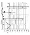
3.2 動作
図9は、本実施形態における初期化期間、アドレス期間及び放電維持期間それぞれでの、PDP20の走査電極Yに対する印加電圧波形、並びに走査電極駆動部11に含まれる各スイッチ素子のオン期間を示す図である。図9では、それぞれのスイッチ素子のオン期間が斜線部で示される。以下、各期間の動作について説明する。3.2 Operation FIG. 9 shows the voltage waveform applied to the scan electrode Y of the
3.2.1 初期化期間
初期化期間は初期化パルス電圧の変化に応じて次の9つのモードI〜IXに分けられる。図9に示すように、モードII、モードV、モードIXにおいて上昇または下降する電圧波形(ランプ波形)が走査電極に印加されている。以下、各モードの動作について説明する。3.2.1 Initialization Period The initialization period is divided into the following nine modes I to IX according to changes in the initialization pulse voltage. As shown in FIG. 9, a voltage waveform (ramp waveform) that rises or falls in mode II, mode V, and mode IX is applied to the scan electrodes. Hereinafter, the operation in each mode will be described.
<モードI>
走査電極駆動部11では、ローサイド走査スイッチ素子Q2Y、第一の分離スイッチ素子QS1、第二の分離スイッチ素子QS2及びハイサイド維持スイッチ素子Q7Yがオン状態に維持される。残りのスイッチ素子はオフ状態に維持される。それにより、走査電極Yは接地電位(≒0)から維持電圧Vsだけ高い電位Vsに維持される。<Mode I>
In
<モードII>
走査電極駆動部11では、ローサイド走査スイッチ素子Q2Y及び第一の分離スイッチ素子QS1がオン状態に維持されたまま、ハイサイド維持スイッチ素子Q7Y及び第二の分離スイッチ素子QS2がオフし、ローサイドランプ波形発生部QR2がオンする。残りのスイッチ素子はオフ状態に維持される。走査電極Yの電位は一定の速度で、接地電位(≒0)から第三の定電圧源の電圧V3だけ低い電位−V3まで下降する。こうして、PDP20の全ての放電セルにおいて一様に印加電圧が、−V3の電位まで比較的緩やかに下降する。それにより、PDP20の全ての放電セルで壁電荷が一様に除去(消去)され、均一化される。このとき、印加電圧の下降速度は小さいので、放電セルの発光は微弱に抑えられる。<Mode II>
In the scan
<モードIII>
走査電極駆動部11では、ローサイド走査スイッチ素子Q2Y及び第一の分離スイッチ素子QS1がオン状態に維持されたまま、ローサイドランプ波形発生部QR2がオフし、第二の分離スイッチ素子QS2及びローサイド維持スイッチ素子Q8Yをオンし、残りのスイッチ素子はオフ状態に維持される。それにより、走査電極Yは接地電位(≒0)に上昇する。<Mode III>
In the
<モードIV>
走査電極駆動部11では、第一の分離スイッチ素子QS1、第二の分離スイッチ素子QS2及びローサイド維持スイッチ素子Q8Yがオン状態に維持されたまま、ローサイド走査スイッチ素子Q2Yをオフし、ハイサイド走査スイッチ素子Q1Yをオンし、残りのスイッチ素子はオフ状態に維持される。それにより、走査電極Yの電位が接地電位(≒0)から第一の電圧源V1の電圧V1だけ高い電位V1まで上昇する。<Mode IV>
In the scan
<モードV>
走査電極駆動部11では、ハイサイド走査スイッチ素子Q1Y及び第二の分離スイッチ素子QS2がオン状態に維持されたまま、第一の分離スイッチ素子QS1及びローサイド維持スイッチ素子Q8Yがオフし、ハイサイドランプ波形発生部QR1がオンする。残りのスイッチ素子はオフ状態に維持される。それにより、走査電極Yの電位が一定の速度で電位Vrに向かって上昇する。またこのとき、第二の分離スイッチ素子QS2を介して、第一の分離スイッチ素子QS1のドレイン電位も上昇する。そして保護回路55の働きによって、第一の分離スイッチ素子QS1のソース電位は上昇し、第一の分離スイッチ素子QS1のソース電位が電位Vsに達したときに、ハイサイド維持スイッチ素子Q7Yのボディーダイオードによって第一の分離スイッチ素子QS1のソース電位がクランプされる。このように、初期化パルス電圧の上限Vrに達する前に(すなわち、第一の分離スイッチ素子QS1のドレイン電位が電位V2に達する前に)、第一の分離スイッチ素子QS1のソース電位は電位VSに達する。このため、第一の分離スイッチ素子QS1のドレイン・ソース間電圧はその耐圧を超えることはない。<Mode V>
In the scan
こうして、PDP20の全ての放電セルに対して一様に、印加電圧が、初期化パルス電圧の上限Vrに向かって比較的緩やかに上昇する。それにより、PDP20の全ての放電セルで一様な壁電荷が蓄積される。そのとき、印加電圧の上昇速度が小さいので、放電セルの発光は微弱に抑えられる。 In this way, the applied voltage uniformly increases for all discharge cells of the
<モードVI>
走査電極駆動部11では、ハイサイド走査スイッチ素子Q1Y、第二の分離スイッチ素子QS2及びハイサイドランプ波形発生部QR1がオン状態に維持されたまま、ハイサイド維持スイッチ素子Q7Yがオンする。残りのスイッチ素子はオフ状態に維持される。走査電極Yの電位が接地電位(≒0)から初期化パルス電圧の上限Vrだけ高い電位を維持する。このとき、保護回路55の働きによってすでに、第一の分離スイッチ素子QS1のソース電位は電位Vsにクランプされている。ハイサイド維持スイッチ素子Q7Yのボディーダイオードの導通状態でハイサイド維持スイッチ素子Q7Yをオンすると、第一の分離スイッチ素子のソース電位が変動しない。なお、図9ではハイサイド維持スイッチ素子Q7Yをオンしているが、ハイサイド維持スイッチ素子Q7Yのボディーダイオードを導通するので、オフしたままでもよい。<Mode VI>
In
こうして、PDP20の全ての放電セルに対して一様に、印加電圧が、初期化パルス電圧の上限Vrまで比較的緩やかに上昇する。それにより、PDP20の全ての放電セルで一様な壁電荷が蓄積される。そのとき、印加電圧の上昇速度が小さいので、放電セルの発光は微弱に抑えられる。 In this way, the applied voltage uniformly increases to all discharge cells of the
<モードVII>
走査電極駆動部11では、ハイサイド走査スイッチ素子Q1Y、第二の分離スイッチ素子QS2及びハイサイド維持スイッチ素子Q7Yがオン状態に維持されたまま、ハイサイドランプ波形発生部QR1がオフし、第一の分離スイッチ素子QS1がオンする。残りのスイッチ素子はオフ状態に維持される。それにより、走査電極Yの電位は電位(Vs+V1)まで下降する。<Mode VII>
In the scan
なお、図9の例では、ハイサイド維持スイッチ素子Q7Yをオンしている。しかし、ハイサイド維持スイッチ素子Q7Yのボディーダイオードが導通するので、ハイサイド維持スイッチ素子Q7Yはオフしたままでもよい。 In the example of FIG. 9, the high side sustain switch element Q7Y is turned on. However, since the body diode of the high side sustain switch element Q7Y conducts, the high side sustain switch element Q7Y may remain off.
<モードVIII>
走査電極駆動部11では、第一の分離スイッチ素子QS1、第二の分離スイッチ素子QS2及びハイサイド維持スイッチ素子Q7Yがオン状態に維持されたまま、ハイサイド走査スイッチ素子Q1Yがオフし、ローサイド走査スイッチ素子Q2Yがオンする。残りのスイッチ素子はオフ状態に維持される。それにより、走査電極Yの電位は電位Vsまで下降する。<Mode VIII>
In the
<モードIX>
走査電極駆動部11では、ローサイド走査スイッチ素子Q2Y及び第一の分離スイッチ素子QS1がオン状態に維持されたまま、ハイサイド維持スイッチ素子Q7Y及び第二の分離スイッチ素子QS2がオフし、ローサイドランプ波形発生部QR2がオンする。残りのスイッチ素子はオフ状態に維持される。走査電極Yの電位は一定の速度で電位-V3まで下降する。<Mode IX>
In the scan
モードIX直前の期間(モードIV〜VIII)では、PDP20のすべての放電セルで一様な壁電荷が蓄積されている。この状態で、モードIXにおいて、モードIV〜VIIIでの印加電圧とは逆極性の比較的緩やか電圧が印加されるので、モードIIとは異なり、全ての放電セルで壁電荷が一様に除去され、均一化される。そのとき印加電圧の下降速度が小さいので、放電セルの発光は微弱に抑えられる。 In the period immediately before mode IX (modes IV to VIII), uniform wall charges are accumulated in all the discharge cells of PDP20. In this state, in mode IX, since a relatively gentle voltage having a polarity opposite to that applied in modes IV to VIII is applied, unlike in mode II, wall charges are uniformly removed in all discharge cells. , Uniform. At that time, since the rate of decrease of the applied voltage is small, the light emission of the discharge cell is suppressed to be weak.
なお、初期化期間中発光をより微弱に抑えるために、モードIV期間中及びモードVの初期の期間に全てのアドレス電極Aに、信号パルス電圧の上限Vaを印加してもよい(アドレス電極Aに印加する信号パルスをオンしてもよい。)。さらに、モードVIII期間中には、全てのアドレス電極Aに印加する信号パルス電圧を上限Vaから接地電位にしてもよい(アドレス電極Aに印加する信号パルスをオフしてもよい。)。 In order to suppress light emission more weakly during the initialization period, the upper limit Va of the signal pulse voltage may be applied to all the address electrodes A during the mode IV period and the initial period of the mode V (address electrode A The signal pulse to be applied to may be turned on.) Further, during the mode VIII, the signal pulse voltage applied to all the address electrodes A may be changed from the upper limit Va to the ground potential (the signal pulse applied to the address electrodes A may be turned off).
3.2.2 アドレス期間
アドレス期間中、走査電極駆動部11では、ローサイドランプ波形発生部QR2、ハイサイド走査スイッチ素子Q1Yがオン状態に維持される。従って、ハイサイド走査スイッチ素子Q1Yのドレインは-V3から第一の定電圧源の電圧V1だけ高い電位Vp(=V1-V3、以下「走査パルス電圧の上限」という。)に維持され、ローサイド走査スイッチ素子Q2Yのソースは-V3に維持される。3.2.2 Address Period During the address period, in the
アドレス期間の開始時、全ての走査電極Yについて、ハイサイド走査スイッチ素子Q1Yがオン状態に維持され、ローサイド走査スイッチ素子Q2Yがオフ状態に維持される。それにより、全ての走査電極Yの電位が一様に走査パルス電圧の上限Vpに維持される。 At the start of the address period, for all scan electrodes Y, the high side scan switch element Q1Y is maintained in the on state and the low side scan switch element Q2Y is maintained in the off state. As a result, the potentials of all the scan electrodes Y are uniformly maintained at the upper limit Vp of the scan pulse voltage.
走査電極駆動部11は続いて、走査電極Yの電位を次のように変化させる(図9に示される走査パルス電圧SP参照)。一つの走査電極Yが選択されると、その走査電極Yに接続されるハイサイド走査スイッチ素子Q1Yがオフし、ローサイド走査スイッチ素子Q2Yがオンする。それにより、その走査電極Yの電位が-V3まで下降する。その走査電極Yの電位が所定時間、-V3に維持されると、その走査電極Yに接続されるローサイド走査スイッチ素子Q2Yがオフし、ハイサイド走査スイッチ素子Q1Yがオンする。それにより、その走査電極Yの電位が走査パルス電圧の上限Vpまで上昇する。走査電極駆動部11は走査電極のそれぞれに接続される走査スイッチ素子対Q1Y、Q2Yについて、上記と同様なスイッチング動作を順次行う。こうして、走査パルス電圧SPが走査電極のそれぞれに対し順次、印加される。 Subsequently, the
アドレス期間中、外部から入力される映像信号に基づきの一つのアドレス電極Aが選択されると、その選択されたアドレス電極Aの電位が所定時間、信号パルス電圧の上限Vaまで上昇する(図示せず)。 When one address electrode A is selected based on a video signal input from the outside during the address period, the potential of the selected address electrode A rises to the upper limit Va of the signal pulse voltage for a predetermined time (not shown). )
例えば、走査パルス電圧SPが一つの走査電極Yに印加され、かつ信号パルス電圧が一つのアドレス電極Aに印加されるとき、その走査電極Yとアドレス電極Aとの間の電圧は他の電極間の電圧より高い。従って、その走査電極Yとアドレス電極Aとの間の交差点に位置する放電セルでは放電が生じる。その放電により、その放電セル表面に新たな壁電荷が蓄積される。 For example, when the scan pulse voltage SP is applied to one scan electrode Y and the signal pulse voltage is applied to one address electrode A, the voltage between the scan electrode Y and the address electrode A is between the other electrodes. Higher than the voltage of. Therefore, discharge occurs in the discharge cell located at the intersection between the scan electrode Y and the address electrode A. Due to the discharge, new wall charges are accumulated on the surface of the discharge cell.
その後、放電維持期間において、走査電極駆動部11と維持電極駆動部12(図示せず)とが交互に、放電維持パルス電圧をそれぞれ、走査電極Yと維持電極Xとに対し印加する(図9参照)。そのとき、アドレス期間中に壁電荷が蓄積された放電セルでは放電が維持されるので、発光が生じる。 Thereafter, in the discharge sustain period, scan
3.2.3 放電維持期間
放電維持期間について説明する。ローサイド走査スイッチ素子Q2Y、第一の分離スイッチ素子QS1及び第二の分離スイッチ素子QS2は常にオン状態に維持される。3.2.3 Discharge sustain period The discharge sustain period will be described. The low-side scanning switch element Q2Y, the first separation switch element QS1, and the second separation switch element QS2 are always maintained in the on state.
ハイサイド回収スイッチ素子Q9Yがオンする直前には、ローサイド維持スイッチ素子Q8Yがオンしており、パネル容量Cpの両端電圧は0Vに維持される。ハイサイド回収スイッチ素子Q9Yがオンすると、回収コンデンサCYと、ハイサイド回収スイッチ素子Q9Yと、第一の回収ダイオードD1と、第一の回収インダクタLY1と、パネル容量Cpとにより、LC共振回路が形成される。これにより、パネル容量Cpの両端電圧はVsまで増加する。残りのスイッチ素子はオフ状態に維持される。 Immediately before the high-side recovery switch element Q9Y is turned on, the low-side sustain switch element Q8Y is turned on, and the voltage across the panel capacitance Cp is maintained at 0V. When the high-side recovery switch element Q9Y is turned on, an LC resonance circuit is formed by the recovery capacitor CY, the high-side recovery switch element Q9Y, the first recovery diode D1, the first recovery inductor LY1, and the panel capacitance Cp. Is done. As a result, the voltage across the panel capacitance Cp increases to Vs. The remaining switch elements are kept off.
次に、ハイサイド回収スイッチ素子Q9Yがオフして、ハイサイド維持スイッチ素子Q7Yがオンすれば、パネル容量Cpの両端電圧はVsに維持される。このとき、ハイサイド維持スイッチ素子Q7Yのドレイン・ソース間電圧は零であるので、ほぼ損失なくオンすることができる(残りのスイッチ素子はオフ状態に維持される)。 Next, when the high side recovery switch element Q9Y is turned off and the high side sustain switch element Q7Y is turned on, the voltage across the panel capacitance Cp is maintained at Vs. At this time, since the drain-source voltage of the high side sustain switch element Q7Y is zero, it can be turned on with almost no loss (the remaining switch elements are maintained in the off state).
所定時間経過後、ハイサイド維持スイッチ素子Q7Yがオフして、ローサイド回収スイッチ素子Q10Yがオンすると(残りのスイッチ素子はオフ状態に維持される)、回収コンデンサCYと、ローサイド回収スイッチ素子Q10Yと、第二の回収ダイオードD2と、第二の回収インダクタLY2と、パネル容量Cpとにより、LC共振回路が形成される。これにより、パネル容量Cpの両端電圧は0まで減少する。 After a predetermined time has elapsed, when the high side sustain switch element Q7Y is turned off and the low side recovery switch element Q10Y is turned on (the remaining switch elements are maintained in the off state), the recovery capacitor CY, the low side recovery switch element Q10Y, An LC resonance circuit is formed by the second recovery diode D2, the second recovery inductor LY2, and the panel capacitance Cp. As a result, the voltage across the panel capacitance Cp decreases to zero.
次に、ローサイド回収スイッチ素子Q10Yがオフして、ローサイド維持スイッチ素子Q8Yがオンすれば、パネル容量Cpの両端電圧は0に維持される。このとき、ローサイド維持スイッチ素子Q8Yのドレイン・ソース間電圧は零であるので、ほぼ損失なくオンすることができる(残りのスイッチ素子はオフ状態に維持される)。 Next, when the low-side recovery switch element Q10Y is turned off and the low-side sustain switch element Q8Y is turned on, the voltage across the panel capacitance Cp is maintained at 0. At this time, since the drain-source voltage of the low-side sustain switch element Q8Y is zero, it can be turned on with almost no loss (the remaining switch elements are maintained in the off state).
走査電極Yの電位が上下するとき、回収コンデンサCYとパネル容量Cpとの間で電力が効率良く交換される。こうして、放電維持パルス電圧の印加時、パネル容量の充放電に起因する無効電力が低減する。 When the potential of the scan electrode Y rises and falls, power is efficiently exchanged between the recovery capacitor CY and the panel capacitance Cp. Thus, the reactive power due to charging / discharging of the panel capacitance is reduced when the sustaining voltage pulse is applied.
3.3 まとめ
以上説明したように本実施形態によれば、保護回路を設けたことにより第一の分離スイッチ素子QS2の耐圧を低下させることができる。第二の分離スイッチ素子の低耐圧化を実現できることから、スイッチ素子が低抵抗となるため、並列接続する第一の分離スイッチ素子数を低減でき、回路規模を削減できる。また、第二の分離スイッチ素子数の低減に伴い実装面積が小さくなることで、基板による配線インピーダンスを低減でき、PDPへの電圧印加時に発生する高周波数成分であるリンギングを低減でき、PDPの動作マージンが拡大する。さらに、放電維持期間での分離スイッチ素子による導通損失が大きく削減されるので、消費電力を低減できる。3.3 Summary According to the present embodiment as described above, the withstand voltage of the first separation switch element QS2 can be lowered by providing the protection circuit. Since the low breakdown voltage of the second separation switch element can be realized, the switch element has a low resistance. Therefore, the number of first separation switch elements connected in parallel can be reduced, and the circuit scale can be reduced. In addition, the mounting area is reduced with the reduction in the number of second separation switch elements, so that the wiring impedance due to the substrate can be reduced, ringing that is a high frequency component generated when voltage is applied to the PDP can be reduced, and the operation of the PDP The margin is expanded. Furthermore, since the conduction loss due to the separation switch element during the discharge sustain period is greatly reduced, power consumption can be reduced.
また、第一の分離スイッチ素子QS1がオフする期間であって第一の分離スイッチ素子QS1のソース電位が電位Vsになっている期間は、保護回路の動作を停止させることで、保護回路の損失を大幅に低下することができる。 In addition, during the period when the first separation switch element QS1 is turned off and the source potential of the first separation switch element QS1 is at the potential Vs, the operation of the protection circuit is stopped, so that the loss of the protection circuit Can be greatly reduced.
実施の形態4
本実施の形態では、実施の形態3のPDP駆動装置に適用可能な保護回路の別の構成を示す。本実施の形態の保護回路は、第一の分離スイッチ素子QS1のソース電位を検出し、その検出値が零(接地電位)になった時点で、停止スイッチ素子S2のゲートに停止信号を自動的に印加し、保護回路の動作を停止させる。図10に本実施形態の保護回路の構成例を示す。Embodiment 4
In the present embodiment, another configuration of a protection circuit applicable to the PDP driving device of the third embodiment is shown. The protection circuit of the present embodiment detects the source potential of the first separation switch element QS1 and automatically sends a stop signal to the gate of the stop switch element S2 when the detected value becomes zero (ground potential). To stop the operation of the protection circuit. FIG. 10 shows a configuration example of the protection circuit of this embodiment.
図10(a)に示す保護回路56aは、図8(a)に示す実施の形態3の保護回路55aの構成に加えて、さらにゲート抵抗R8及び比較器OP1を備える。また、停止スイッチ素子S2はPチャネルスイッチを用いている。 The
停止スイッチ素子S2のソースはツェナーダイオードZD1のカソードと接続し、停止スイッチ素子S2のドレインは第二の分離スイッチ素子QS2のソースと接続する。ゲート抵抗R8は停止スイッチ素子S2のゲート・ソース間に接続される。比較器OP1の出力は、停止スイッチ素子S2のゲートに接続される。比較器OP1の負入力端子は維持電源Vsの正極に接続され、正入力端子は第一の分離スイッチ素子QS1のソースに接続される。 The source of the stop switch element S2 is connected to the cathode of the Zener diode ZD1, and the drain of the stop switch element S2 is connected to the source of the second separation switch element QS2. The gate resistor R8 is connected between the gate and source of the stop switch element S2. The output of the comparator OP1 is connected to the gate of the stop switch element S2. The negative input terminal of the comparator OP1 is connected to the positive electrode of the sustain power source Vs, and the positive input terminal is connected to the source of the first separation switch element QS1.
保護回路56aは、第一の分離スイッチ素子QS1がオフしている期間で且つ、停止スイッチ素子S2のゲートに停止信号が印加されていない期間に動作する。停止信号は、比較器OP1により第一の分離スイッチ素子QS1のソース電位に基づいて生成される。 The
具体的には、第一の分離スイッチ素子QS1がオフしている期間において、比較器OP1は第第一の分離スイッチ素子QS1のソース電位を入力し、ソース電位が電位Vsより大きければ、停止スイッチ素子S2のゲートにHレベルの信号(作動信号)を印加する。この場合、停止スイッチ素子S2のゲート・ソース間電圧は零となるため、停止スイッチ素子S2はオフ状態となり、保護回路56aは第二の分離スイッチ素子QS2のドレイン・ソース間電圧を一定に制限する動作を行う。 Specifically, during the period when the first separation switch element QS1 is off, the comparator OP1 inputs the source potential of the first separation switch element QS1, and if the source potential is greater than the potential Vs, the stop switch An H level signal (operation signal) is applied to the gate of the element S2. In this case, since the gate-source voltage of the stop switch element S2 becomes zero, the stop switch element S2 is turned off, and the
第一の分離スイッチ素子QS1のソース電位がVsになると、比較器OP1はLレベルの信号(停止信号)を停止スイッチ素子S2のゲートに印加する。これにより、停止スイッチ素子S2のゲート・ソース間には所定電圧が印加されるため、停止スイッチ素子S2がオンする。停止スイッチ素子S2がオンすると、第二の検出抵抗R3の両端が短絡されるので保護用スイッチ素子S1は動作せず、保護回路56aは動作しない。つまり、このとき、たとえ第一の分離スイッチ素子QS1のドレイン・ソース間電圧が保護回路51aの設定電圧Vcを超えたとしても保護回路51aは動作せず、第一の制限抵抗R1に電流は流れず、電流消費を抑制できる。 When the source potential of the first separation switch element QS1 becomes Vs, the comparator OP1 applies an L level signal (stop signal) to the gate of the stop switch element S2. As a result, a predetermined voltage is applied between the gate and source of the stop switch element S2, so that the stop switch element S2 is turned on. When the stop switch element S2 is turned on, both ends of the second detection resistor R3 are short-circuited, so that the protection switch element S1 does not operate and the
図10(b)に示す保護回路56bは、図8(b)に示す実施の形態3の保護回路55bの構成に加えて、さらにゲート抵抗R8及び比較器OP1を含んでいる。また、停止スイッチ素子S2はPチャネルスイッチを用いている。図10(c)に示す保護回路56cは、図8(c)に示す実施の形態3の保護回路55cの構成に加えて、さらにゲート抵抗R8及び比較器OP1を含んでいる。これらの保護回路56b、56cの動作はそれぞれ基本的に図8(b)、(c)に示す保護回路55b、55cのものと同様であるが、第一の分離スイッチ素子QS1のソース電位を検出し、検出したソース電位が電位Vsになったときに保護回路56b、56cの動作を自動的に停止させる点が異なる。 The
本実施の形態の保護回路は、実施の形態3の場合と同様の効果を奏する。特に、本実施の形態の保護回路は、第一の分離スイッチ素子のソース電位に基づき自動的に保護回路の停止動作を制御することができる。 The protection circuit of the present embodiment has the same effect as that of the third embodiment. In particular, the protection circuit of the present embodiment can automatically control the stop operation of the protection circuit based on the source potential of the first separation switch element.
本発明は、低消費電力等が要求されるプラズマディスプレイの駆動装置に有用である。 The present invention is useful for a plasma display driving apparatus that requires low power consumption and the like.
1 入力端子
10 PDP駆動装置
11 走査電極駆動部
12 維持電極駆動部
13 アドレス電極駆動部
20 プラズマディスプレイパネル(PDP)
30 制御部
50、50b、50c、51a〜51c、55、55a〜55c、56a〜56c 保護回路
1Y 走査パルス発生部
2Y、5Y〜9Y 初期化パルス発生部
3Y 放電維持パルス発生部
4Y 回収回路
Q1Y ハイサイド走査スイッチ素子
Q2Y ローサイド走査スイッチ素子
Q7Y ハイサイド維持スイッチ素子
Q8Y ローサイド維持スイッチ素子
QR1、QR3 ハイサイドランプ波形発生部
QR2 ローサイドランプ波形発生部
QS1、QS2 分離スイッチ素子
V1、V2、V3 直流電源
Vs 維持電源DESCRIPTION OF
30
Claims (9)
Translated fromJapaneseプラズマディスプレイパネルの発光のための放電を維持する電圧を与える維持電源と、
前記維持電源の正極への電流の流入及び/又は前記維持電源の負極からの電流の流出を阻止可能な分離スイッチ素子と、
前記分離スイッチ素子と並列に接続され、前記分離スイッチ素子への印加電圧を制限する保護回路とを備え、
前記保護回路は、停止信号により前記保護回路の動作を停止させる停止手段を有する、
プラズマディスプレイパネルの駆動装置A plasma display panel driving device comprising a sustain electrode, a scan electrode, and an address electrode, and comprising a plurality of discharge cells,
A maintenance power supply for applying a voltage to maintain a discharge for light emission of the plasma display panel;
A separation switch element capable of preventing inflow of current to the positive electrode of the maintenance power source and / or outflow of current from the negative electrode of the maintenance power source;
A protection circuit that is connected in parallel with the separation switch element and limits a voltage applied to the separation switch element;
The protection circuit has stop means for stopping the operation of the protection circuit by a stop signal.
Driving device for plasma display panel
前記プラズマディスプレイパネルを駆動する請求項1ないし8のいずれか1つに記載のプラズマディスプレイパネルの駆動装置と
を備える、プラズマディスプレイ。A plasma display panel capable of displaying an image by light emission caused by discharge between the electrodes;
A plasma display comprising: the plasma display panel driving apparatus according to claim 1, wherein the plasma display panel is driven.
Priority Applications (1)
| Application Number | Priority Date | Filing Date | Title |
|---|---|---|---|
| JP2006109630AJP2007286083A (en) | 2006-04-12 | 2006-04-12 | Plasma display driving apparatus and plasma display |
Applications Claiming Priority (1)
| Application Number | Priority Date | Filing Date | Title |
|---|---|---|---|
| JP2006109630AJP2007286083A (en) | 2006-04-12 | 2006-04-12 | Plasma display driving apparatus and plasma display |
Publications (1)
| Publication Number | Publication Date |
|---|---|
| JP2007286083Atrue JP2007286083A (en) | 2007-11-01 |
Family
ID=38757948
Family Applications (1)
| Application Number | Title | Priority Date | Filing Date |
|---|---|---|---|
| JP2006109630APendingJP2007286083A (en) | 2006-04-12 | 2006-04-12 | Plasma display driving apparatus and plasma display |
Country Status (1)
| Country | Link |
|---|---|
| JP (1) | JP2007286083A (en) |
Cited By (1)
| Publication number | Priority date | Publication date | Assignee | Title |
|---|---|---|---|---|
| WO2012017647A1 (en)* | 2010-08-04 | 2012-02-09 | パナソニック株式会社 | Plasma display panel driving method and plasma display apparatus |
- 2006
- 2006-04-12JPJP2006109630Apatent/JP2007286083A/enactivePending
Cited By (1)
| Publication number | Priority date | Publication date | Assignee | Title |
|---|---|---|---|---|
| WO2012017647A1 (en)* | 2010-08-04 | 2012-02-09 | パナソニック株式会社 | Plasma display panel driving method and plasma display apparatus |
Similar Documents
| Publication | Publication Date | Title |
|---|---|---|
| JPWO2007060845A1 (en) | PDP driving device and plasma display | |
| US20120007847A1 (en) | Plasma display device | |
| US20070188416A1 (en) | Apparatus for driving plasma display panel and plasma display | |
| CN100403366C (en) | Device and method for driving plasma display panel | |
| US8199072B2 (en) | Plasma display device and method of driving the same | |
| US7852292B2 (en) | Plasma display apparatus and driving method thereof | |
| KR100425487B1 (en) | Apparatus Of Driving Plasma Display Panel | |
| KR100590112B1 (en) | Plasma display device and driving method thereof | |
| US8294636B2 (en) | Plasma display device and method of driving the same | |
| JP5110773B2 (en) | Plasma display panel drive device | |
| CN102047311A (en) | Plasma display panel driving method | |
| JPWO2008059735A1 (en) | Plasma display panel driving method and plasma display device | |
| CN100433096C (en) | Plasma display device and driving method thereof | |
| JP2007286083A (en) | Plasma display driving apparatus and plasma display | |
| US20050190125A1 (en) | Capacitive load driver and plasma display | |
| US7474278B2 (en) | Plasma display apparatus and method of driving the same | |
| CN101351832A (en) | Plasma display panel driving method and plasma display device | |
| JPWO2007088804A1 (en) | Plasma display driving apparatus and plasma display | |
| KR100658332B1 (en) | Driving apparatus for plasma display panel and driving method thereof | |
| JP2005338842A (en) | Plasma display apparatus | |
| KR100732583B1 (en) | Plasma display apparatus | |
| JPWO2007094293A1 (en) | Plasma display panel driving method and plasma display device | |
| JPWO2008072458A1 (en) | Plasma display apparatus and driving method of plasma display panel | |
| KR100658331B1 (en) | Driving apparatus for plasma display panel and driving method thereof | |
| KR100761291B1 (en) | Plasma display device |