JP2007266974A - Optical communication system, optical id reader, and information reading method - Google Patents
Optical communication system, optical id reader, and information reading methodDownload PDFInfo
- Publication number
- JP2007266974A JP2007266974AJP2006089009AJP2006089009AJP2007266974AJP 2007266974 AJP2007266974 AJP 2007266974AJP 2006089009 AJP2006089009 AJP 2006089009AJP 2006089009 AJP2006089009 AJP 2006089009AJP 2007266974 AJP2007266974 AJP 2007266974A
- Authority
- JP
- Japan
- Prior art keywords
- optical
- tag
- identification information
- light
- reader
- Prior art date
- Legal status (The legal status is an assumption and is not a legal conclusion. Google has not performed a legal analysis and makes no representation as to the accuracy of the status listed.)
- Granted
Links
Images


Classifications
- G—PHYSICS
- G06—COMPUTING OR CALCULATING; COUNTING
- G06K—GRAPHICAL DATA READING; PRESENTATION OF DATA; RECORD CARRIERS; HANDLING RECORD CARRIERS
- G06K7/00—Methods or arrangements for sensing record carriers, e.g. for reading patterns
- G06K7/10—Methods or arrangements for sensing record carriers, e.g. for reading patterns by electromagnetic radiation, e.g. optical sensing; by corpuscular radiation
- G06K7/10544—Methods or arrangements for sensing record carriers, e.g. for reading patterns by electromagnetic radiation, e.g. optical sensing; by corpuscular radiation by scanning of the records by radiation in the optical part of the electromagnetic spectrum
- G06K7/10821—Methods or arrangements for sensing record carriers, e.g. for reading patterns by electromagnetic radiation, e.g. optical sensing; by corpuscular radiation by scanning of the records by radiation in the optical part of the electromagnetic spectrum further details of bar or optical code scanning devices
- G06K7/1097—Optical sensing of electronic memory record carriers, such as interrogation of RFIDs with an additional optical interface
- G—PHYSICS
- G06—COMPUTING OR CALCULATING; COUNTING
- G06K—GRAPHICAL DATA READING; PRESENTATION OF DATA; RECORD CARRIERS; HANDLING RECORD CARRIERS
- G06K19/00—Record carriers for use with machines and with at least a part designed to carry digital markings
- G06K19/06—Record carriers for use with machines and with at least a part designed to carry digital markings characterised by the kind of the digital marking, e.g. shape, nature, code
- G06K19/067—Record carriers with conductive marks, printed circuits or semiconductor circuit elements, e.g. credit or identity cards also with resonating or responding marks without active components
- G06K19/07—Record carriers with conductive marks, printed circuits or semiconductor circuit elements, e.g. credit or identity cards also with resonating or responding marks without active components with integrated circuit chips
- G06K19/0723—Record carriers with conductive marks, printed circuits or semiconductor circuit elements, e.g. credit or identity cards also with resonating or responding marks without active components with integrated circuit chips the record carrier comprising an arrangement for non-contact communication, e.g. wireless communication circuits on transponder cards, non-contact smart cards or RFIDs
- G06K19/0728—Record carriers with conductive marks, printed circuits or semiconductor circuit elements, e.g. credit or identity cards also with resonating or responding marks without active components with integrated circuit chips the record carrier comprising an arrangement for non-contact communication, e.g. wireless communication circuits on transponder cards, non-contact smart cards or RFIDs the arrangement being an optical or sound-based communication interface
Landscapes
- Engineering & Computer Science (AREA)
- Physics & Mathematics (AREA)
- General Physics & Mathematics (AREA)
- Theoretical Computer Science (AREA)
- Electromagnetism (AREA)
- Microelectronics & Electronic Packaging (AREA)
- Computer Hardware Design (AREA)
- Computer Networks & Wireless Communication (AREA)
- General Health & Medical Sciences (AREA)
- Computer Vision & Pattern Recognition (AREA)
- Artificial Intelligence (AREA)
- Toxicology (AREA)
- Health & Medical Sciences (AREA)
- Optical Communication System (AREA)
Abstract
Description
Translated fromJapanese本発明は光通信システム、光IDリーダ及び情報読取方法に関し、小型の無線ICチップから識別情報を読み取る場合に適用して好適なものである。 The present invention relates to an optical communication system, an optical ID reader, and an information reading method, and is suitable for application when reading identification information from a small wireless IC chip.
近年、バーコードに代わる物品の識別又は管理技術として、RFID(Radio Frequency IDentification)が注目されている。 In recent years, RFID (Radio Frequency IDentification) has been attracting attention as a technology for identifying or managing an article instead of a barcode.
このRFIDでは、無線ICタグ(あるいは無線ICチップ)と呼ばれる小型の無線装置内に固有の識別情報を記憶し、この識別情報に基づいて物品の識別又は管理が行われる。 In this RFID, unique identification information is stored in a small wireless device called a wireless IC tag (or wireless IC chip), and an article is identified or managed based on this identification information.
この無線ICタグや、該無線ICタグから送信される無線信号から識別情報を読み取るリーダとしては種々のものが提案され、なかには、無線ICタグと、リーダとが光通信により識別情報を授受するようにしたものが提案されている(例えば特許文献1参照)。 Various readers have been proposed as readers for reading identification information from the wireless IC tag and a wireless signal transmitted from the wireless IC tag. Among them, the wireless IC tag and the reader exchange identification information by optical communication. (See, for example, Patent Document 1).
この特許文献1では、光IDリーダは、光IDタグに向けて光ビームを放射し、光IDタグから放射された光信号を受光して、光IDタグに固有の識別情報を読み取る光IDリーダ部を備えている。 In this
一方、光IDタグは、固有の識別情報を記憶するメモリと、光IDリーダから放射された光ビームを、メモリに記憶された識別情報で変調して光信号に変換する光変換部と、この変調された光信号を光ビームの入射方向に反射する光反射部とを備えている。 On the other hand, the optical ID tag includes a memory that stores unique identification information, a light conversion unit that modulates the light beam emitted from the optical ID reader with the identification information stored in the memory, and converts the light beam into an optical signal. And a light reflecting portion for reflecting the modulated optical signal in the incident direction of the light beam.
この特許文献1によれば、空間中に近接して存在する複数の光IDタグの識別を離れた場所から行うことが可能となり、光IDリーダをリモコンのように用いて読み取ることが可能となる。
ところがかかる構成の光IDタグでは、同じような入射角から複数の光ビームが放射された場合、反射する光はその入射方向に集まる(すなわち輻輳状態となる)ことによって、当該入射角から光ビームを放射した光IDリーダそれぞれに対し、識別情報が伝達されないあるいは同一でなる複数の識別情報が同時に伝達されるという問題があった。 However, in the optical ID tag having such a configuration, when a plurality of light beams are radiated from the same incident angle, the reflected light gathers in the incident direction (that is, enters a converging state), so that the light beam is emitted from the incident angle. There is a problem that identification information is not transmitted to each of the optical ID readers that radiate the light, or a plurality of identification information that is the same is transmitted simultaneously.
本発明は以上の点を考慮してなされたもので、識別情報を適切に伝達させ得る光通信システム、光IDリーダ及び情報読取方法を提案しようとするものである。 The present invention has been made in view of the above points, and intends to propose an optical communication system, an optical ID reader, and an information reading method capable of appropriately transmitting identification information.
かかる課題を解決するため本発明は、光を通信媒体として、光IDタグと光IDリーダとの間で識別情報を通信する光通信システムであって、光IDタグには、識別情報を保持する保持手段と、照射される光をその入射方向に反射させる反射手段と、反射された反射光を、保持手段に保持された識別情報に基づいて変調する変調手段とを設け、光IDリーダには、乱数を発生する乱数発生手段と、乱数に対して固有の発信周波数の光を放射する放射手段と、放射方向から到来する反射光を光電変換する光電変換手段と、光電変換手段により光電変換された結果得られる信号から、発信周波数の信号成分を抽出する抽出手段と、信号成分を復調する復調手段とを設けるようにした。 In order to solve such a problem, the present invention is an optical communication system that communicates identification information between an optical ID tag and an optical ID reader using light as a communication medium, and the optical ID tag holds the identification information. The optical ID reader includes a holding unit, a reflecting unit that reflects the irradiated light in the incident direction, and a modulation unit that modulates the reflected light reflected based on the identification information held in the holding unit. A random number generating means for generating a random number, a radiating means for emitting light having a transmission frequency unique to the random number, a photoelectric converting means for photoelectrically converting reflected light coming from the radiation direction, and photoelectrically converted by the photoelectric converting means. An extraction means for extracting the signal component of the transmission frequency from the signal obtained as a result and a demodulation means for demodulating the signal component are provided.
この光通信システムでは、その光IDリーダによって放射され、照射対象となった光IDタグから戻り光として放射される反射光に対して、他の光IDタグから放射される反射光が輻輳した状態であったとしても、当該光IDリーダは、照射対象となった光IDタグから戻り光として放射される反射光に重畳される識別情報を抽出することができる。したがって、この光通信システムでは、光IDタグに近接して他の光IDタグがあり、かつその他の光IDタグに対して同じような入射角から光が照射された状況下にあったとしても、読取対象とされる光IDタグに保持された識別情報を、光IDリーダが読み取ることが可能となる。 In this optical communication system, the reflected light radiated from the other optical ID tag is congested with the reflected light radiated by the optical ID reader and radiated as the return light from the irradiated optical ID tag. Even if it is, the said optical ID reader can extract the identification information superimposed on the reflected light radiated | emitted as return light from the optical ID tag used as irradiation object. Therefore, in this optical communication system, even if there is another optical ID tag in the vicinity of the optical ID tag and the other optical ID tag is irradiated with light from the same incident angle, The optical ID reader can read the identification information held in the optical ID tag to be read.
また本発明は、光を通信媒体として、識別情報が保持された光IDタグとの間で通信する光IDリーダであって、乱数を発生する乱数発生手段と、乱数に対して固有の発信周波数の光を放射する放射手段と、放射手段から光IDタグに放射され、該光IDタグによってその放射方向に反射され、かつ識別情報に基づいて変調された反射光を光電変換する光電変換手段と、光電変換手段により光電変換された結果得られる信号から、発信周波数の信号成分を抽出する抽出手段と、信号成分を復調する復調手段とを設けるようにした。 The present invention also provides an optical ID reader that communicates with an optical ID tag holding identification information using light as a communication medium, random number generating means for generating a random number, and a transmission frequency unique to the random number. And a photoelectric conversion means for photoelectrically converting the reflected light emitted from the radiation means to the optical ID tag, reflected by the optical ID tag in the radiation direction and modulated based on the identification information The extraction means for extracting the signal component of the transmission frequency from the signal obtained as a result of the photoelectric conversion by the photoelectric conversion means and the demodulation means for demodulating the signal component are provided.
この光IDリーダでは、その光IDリーダによって放射され、照射対象となった光IDタグから戻り光として放射される反射光に対して、他の光IDタグから放射される反射光が輻輳した状態であったとしても、照射対象となった光IDタグから戻り光として放射される反射光に重畳される識別情報を抽出することができる。したがって、この光IDリーダでは、光IDタグに近接して他の光IDタグがあり、かつその他の光IDタグに対して同じような入射角から光が照射された状況下にあったとしても、読取対象とされる光IDタグに保持された識別情報を読み取ることが可能となる。 In this optical ID reader, the reflected light radiated from the other optical ID tag is congested with the reflected light radiated by the optical ID reader and radiated as return light from the irradiated optical ID tag. Even if it is, the identification information superimposed on the reflected light radiated | emitted as return light from the optical ID tag used as irradiation object can be extracted. Therefore, in this optical ID reader, even if there is another optical ID tag close to the optical ID tag and the other optical ID tag is irradiated with light from the same incident angle, The identification information held in the optical ID tag to be read can be read.
さらに本発明は、光を通信媒体として、光IDタグに保持された識別情報を読み取る情報読取方法であって、乱数発生手段から乱数を発生させる第1のステップと、乱数に対して固有の発信周波数の光を放射手段から放射させる第2のステップと、放射手段から光IDタグに放射され、該光IDタグによってその放射方向に反射され、かつ識別情報に基づいて変調された反射光に対する光電変換結果として得られる信号から、発信周波数の信号成分を抽出手段に抽出させる第3のステップと、信号成分を復調手段に復調させる第4のステップとを設けるようにした。 Furthermore, the present invention is an information reading method for reading identification information held in an optical ID tag using light as a communication medium, the first step of generating a random number from a random number generating means, and a transmission unique to the random number. A second step of radiating light of a frequency from the radiating means; and a photoelectric for reflected light that is radiated from the radiating means to the optical ID tag, reflected in the radiation direction by the optical ID tag, and modulated based on the identification information A third step for causing the extraction means to extract the signal component of the transmission frequency from the signal obtained as a conversion result and a fourth step for allowing the demodulation means to demodulate the signal component are provided.
従って、この情報読取方法では、その光IDリーダによって放射され、照射対象となった光IDタグから戻り光として放射される反射光に対して、他の光IDタグから放射される反射光が輻輳した状態であったとしても、照射対象となった光IDタグから戻り光として放射される反射光に重畳される識別情報をその光IDリーダが抽出することができる。したがって、この情報読取方法では、光IDタグに近接して他の光IDタグがあり、かつその他の光IDタグに対して同じような入射角から光が照射された状況下にあったとしても、読取対象とされる光IDタグに保持された識別情報をその光IDリーダが読み取ることが可能となる。 Therefore, in this information reading method, the reflected light emitted from the other optical ID tag is congested with respect to the reflected light emitted as the return light from the optical ID tag irradiated by the optical ID reader. Even in this state, the optical ID reader can extract the identification information superimposed on the reflected light emitted as the return light from the optical ID tag that is the irradiation target. Therefore, in this information reading method, even if there is another optical ID tag in the vicinity of the optical ID tag and the other optical ID tag is irradiated with light from the same incident angle, Thus, the optical ID reader can read the identification information held in the optical ID tag to be read.
本発明によれば、光IDタグに近接して他の光IDタグがあり、かつその他の光IDタグに対して同じような入射角から光が照射された状況下にあったとしても、読取対象とされる光IDタグに保持された識別情報をその光IDリーダが読み取ることができるようにしたことにより、識別情報を適切に伝達させ得る光通信システム、光IDリーダ及び情報読取方法を実現することができる。 According to the present invention, even if there is another optical ID tag in the vicinity of the optical ID tag and the other optical ID tag is irradiated with light from the same incident angle, the reading is performed. Realizing an optical communication system, an optical ID reader, and an information reading method capable of appropriately transmitting the identification information by enabling the optical ID reader to read the identification information held in the target optical ID tag can do.
以下図面について、本発明を適用した一実施の形態を詳述する。 Hereinafter, an embodiment to which the present invention is applied will be described in detail with reference to the drawings.
(1)本実施の形態による光通信システムの全体構成
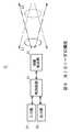
図1において、本実施の形態による光通信システム1の全体構成を示し、複数の光IDタグ2i(i=1、2、3、……、又はm(mは整数))と、複数の光IDリーダ3j(j=1、2、3、……、又はn(nは整数))とによって構成される。(1) Overall Configuration of Optical Communication System According to this Embodiment FIG. 1 shows the overall configuration of an
光IDタグ2iは、それぞれ、所定の物品に設けられるものであり、当該光IDタグ2iには、設置対象となるその物品に関する識別情報が保持される。 Each of the optical ID tags 2i is provided on a predetermined article, and the optical ID tag 2i holds identification information regarding the article to be installed.
具体的には、例えば、光IDタグ21〜2mが製品管理に用いられる場合、各製品に対して光IDタグ2iがそれぞれ設けられ、当該光IDタグ2iには、製品の製造番号及び製造年月日など、その製品に関する製造情報が識別情報として保持される。Specifically, for example, when the
また例えば、光IDタグ21〜2mが情報提供に用いられる場合、各広告媒体に対して光IDタグ2iがそれぞれ設けられ、当該光IDタグ2iには、自社のホームページのURL(Uniform Resource Locater)や、広告製品に関する情報など、その広告媒体に関する提供情報が識別情報として保持される。Further, for example, when the
これら光IDタグ2iは、照射される光ビームL1を、その光ビームの照射方向に反射させるとともに自己に保持される識別情報に基づいて変調し、この結果得られる反射光ビームL2を放射するようになされている。 These optical ID tags 2i modulate the irradiated light beam L1 in the irradiation direction of the light beam and modulate it based on the identification information held by itself, and emit the resulting reflected light beam L2. Has been made.
一方、光IDリーダ3jは、それぞれ、専用の可搬型端末として形成され又は携帯電話機PDA(Personal Digital Assistants)等の可搬型端末に搭載されるものであり、個々のユーザに割り当てられるものである。 On the other hand, each of the optical ID readers 3j is formed as a dedicated portable terminal or mounted on a portable terminal such as a mobile phone PDA (Personal Digital Assistants), and is assigned to each user.
光IDタグ2iに保持される識別情報を読み取る場合、ユーザは、自己に割り当てられた光IDリーダ3jを、読取対象の光IDタグ2iに向けて、該光IDリーダ3jから光ビームL1を放射させるようになされている。 When reading the identification information held in the optical ID tag 2i, the user directs the optical ID reader 3j assigned to the optical ID tag 2i toward the optical ID tag 2i to be read, and emits the light beam L1 from the optical ID reader 3j. It is made to let you.
この場合、光IDリーダ3jは、その光ビームが読取対象の光IDタグ2iから反射された反射光L2に基づいて、その反射光に重畳された該光IDタグ2iの識別情報を抽出するようになされている。 In this case, the optical ID reader 3j extracts the identification information of the optical ID tag 2i superimposed on the reflected light based on the reflected light L2 reflected by the optical beam from the optical ID tag 2i to be read. Has been made.
このようにこの光通信システム1は、ユーザに対して、光IDリーダ3jをあたかもリモートコントローラとして用いさせることができるようになされている。 As described above, the
(2)光IDタグの構成
次に、光IDタグ21〜2mの構成について説明するが、これら光IDタグ21〜2mの構成は同一であるため、説明の便宜上、ここでは光IDタグ21の構成について図2を用いて説明する。(2) Configuration of Optical ID Tag Next, the configuration of the
この図2において、光IDタグ21は、受光部11、蓄電部12、反射量変換部13及びメモリ14を有し、該反射量変換部13は、反射板21a、LCD(Liquid Crystal Display)21b及び偏向板21cを順次積層した構造でなる光学ユニット21と、LCD21b及びメモリ14に結線された変調回路22とよって構成される。In FIG. 2, the optical ID tag2 1, the light receiving unit 11,
この光IDタグ21では、例えば光IDリーダ31から光ビームL1が照射された場合、受光部11は、この光ビームL1を光電変換する。蓄電部12は、この光電変換に応じて誘起される電圧を蓄え、所定の閾値を越えると、該電圧を反射量変換部13の変調回路22に供給する。In the optical ID tag2 1, for example, when the light beam L1 from the optical ID reader3 1 is irradiated, the light receiving unit 11, the light beam L1 is converted photoelectrically. The
変調回路22は、蓄電部12から供給される電圧を待ち受け、該電圧を受けた場合には変調処理を開始する(図3:SP0)。すなわち変調回路22は、蓄電部12から供給される電圧を駆動電圧として起動し(図3:SP1)、メモリ14に記憶された識別情報を読み出す(図3:SP2)。 The
そして変調回路22は、例えばマンチェスターコーディングと呼ばれる変調方式に基づいて、蓄電部12から供給される電圧を、メモリ14から読み出した記憶された識別情報に応じて変調し、この変調結果を光学ユニット21のLCD21bに与える(図3:SP3)。LCD21bでは、この識別情報に応じた電圧の可変に伴って、その液晶配向が変化することになる。 The
変調回路22は、かかるLCD21bの液晶配向を、蓄電部12からの電圧供給が停止されるまで可変し続け、該電圧供給が停止された場合には(図3:SP4(Y))、変調処理を終了する(図3:SP5)。 The
一方、この反射量変換部13の光学ユニット21では、光IDリーダ3から照射される光ビームL1は、偏向板21cを介して、特定の偏光成分の光のみが通過し、該偏向板21cによって選定された光は、反射板21aを介して、該反射板21aの入射方向(つまり照射対象の光IDリーダ3の方向)に反射する。 On the other hand, in the
そして、反射板21aによってその入射方向に反射された光は、LCD21Bを介して、該LCD21Bでの液晶配向にしたがってその偏光状態が可変し、この偏光状態に応じた出射光量となり、この光が偏向板21cを介して反射光L2として出射する。 Then, the light reflected by the
したがって、光IDリーダ31から反射量変換部13に照射される光ビームL1が、例えば図4(A)に示すように単位時間当たり一定の光量のものとした場合、その光ビームL1が照射された光IDタグ21から放射される反射光L2は、例えば図4(B)に示すように、メモリ14に記憶された識別情報に応じて可変された状態となる。Therefore, when the light beam L1 emitted from the optical ID reader 31 to the reflection amount conversion unit 13, and for example, Figure 4 as a constant amount of light per unit time (A), a the light beam L1 is irradiated reflected light L2 emitted from the
このように光IDタグ21は、バッテリーレス状態において、光IDリーダ31から照射される光ビームL1の反射光L2の出射光量を、メモリ14に記憶された識別情報に応じて可変してその反射光L2に識別情報を重畳し、当該識別情報を光IDリーダ31に伝達することができるようになされている。Thus the
ここで、この実施の形態における光IDタグ21においては、かかる受光部11、蓄電部12、反射量変換部13及びメモリ14を、樹脂製の薄厚の筺体に収納するようになされており、これにより筺体外からの塵や水分の流入を防止しかつ簡易に持ち運びし得るようになされている。Here, in the
具体的には、例えば図5に示すように、蓄電部12は、矩形状でなる薄厚の筺体BD内の基板BSの所定位置に設けられ、受光部11は、該基板BSにおける一方の表面(光ビームL1が入射される側の面)の所定位置に設けられる。この受光部11の近傍であって基板BSの中央には、光学ユニット21が設けられ、該基板における他方の表面の所定位置には、変調回路22とメモリ14とがICチップCPとして設けられる。 Specifically, as shown in FIG. 5, for example, the
この図5に示す収納構造によれば、筺体BD表面のうち厚み方向における表面の一方だけを、光IDリーダ3jに対する光ビームL1の入射面とすることができ、基板BSの同一表面上にICチップCP及び光学ユニット21を設ける場合に比して、該光学ユニット21及び受光部11の実装面積を大きく確保することが可能となる。 According to the storage structure shown in FIG. 5, only one of the surfaces in the thickness direction among the surfaces of the housing BD can be the incident surface of the light beam L1 with respect to the optical ID reader 3j, and the IC is formed on the same surface of the substrate BS. Compared with the case where the chip CP and the
(3)光IDリーダの構成
次に、光IDリーダ31〜3nの構成について説明するが、これら光IDリーダ31〜3nの構成は同一であるため、説明の便宜上、ここでは光IDリーダ31の構成について図6を用いて説明する。(3) Configuration of Optical ID Reader Next, the configuration of the optical ID readers 31 to 3n will be described. Since the configuration of these optical ID readers 31 to 3n is the same, for the sake of convenience of explanation, here, will be described with reference to FIG. 6 the structure of ID readers3 1.
この図6において、光IDリーダ31は、該光IDリーダ3全体の制御を司る制御回路30に対して、ユーザ操作に応ずる各種命令を送出する入力部31と、当該命令に対する処理やユーザ操作の内容を視覚及び聴覚を通じて知らせる出力部32と、光ビームを放射しその戻り光に重畳された識別情報を抽出する情報抽出部33とを結線して構成される。In FIG. 6, the optical ID reader 31, the control circuit 30 which controls the optical ID reader 3 overall control, an
この制御回路30は、CPU(Central Processing Unit)、ROM(Read Only Memory)、RAM(Random Access Memory)、クロック発生器及びフラッシュメモリを含むコンピュータ構成となっている。 The control circuit 30 has a computer configuration including a CPU (Central Processing Unit), a ROM (Read Only Memory), a RAM (Random Access Memory), a clock generator, and a flash memory.
制御回路30は、入力部31から識別情報の読み取り命令を受けた場合、情報抽出部33を介して光IDタグ2に保持された識別情報を取得し、この識別情報をフラッシュメモリに記憶するとともに、当該識別情報の内容を出力部32を介して通知するようになされている。 When receiving a read instruction of identification information from the
ここで、この実施の形態における情報抽出部33を図7に示す。この図7において、情報抽出部33は、送信処理部41と、受信処理部42とによって構成される。 Here, FIG. 7 shows the
送信処理部41は、乱数発生器51、信号発生部52、振幅増幅器53及びLED(Light Emitting Diode)54でなり、この乱数発生器51は、制御回路30(図6)からの制御命令を受ける度に乱数を生成し、これを信号発生部52に送出する。 The transmission processing unit 41 includes a
この信号発生部52には、乱数と、発信周波数との対応付けがテーブルとして保持されている。信号発生部52は、このテーブルに基づいて、乱数発生器51から供給される乱数に対応する発信周波数を選択し、該選択した発信周波数の値を受信処理部42に送出する。 The
また信号発生部52は、選択した発信周波数の信号を生成し、これを振幅増幅器53を介してLED54に印加する。この結果、LED54から、乱数に応ずる発信周波数の光ビームL1(図6)が放射される。 The
このようにして送信処理部41は、その都度異なる発信周波数の光ビームL1を放射することができるようになされている。 In this way, the transmission processing unit 41 can emit the light beam L1 having a different transmission frequency each time.
一方、受信処理部42は、PD(Photo Diode)55、検波部56、BPF(Band Pass Filter)57及び復調回路58でなり、このPD55は、光IDタグ2によって識別情報が重畳された状態で放射される反射光L2(図6)を光電変換し、この結果得られる交流信号を検波器56に送出する。 On the other hand, the reception processing unit 42 includes a PD (Photo Diode) 55, a
検波部56は、この交流信号を検波し、該検波した交流信号の包絡線を検波信号としてBPF57に送出する。 The
BPF57は、送信処理部41の信号発生部52から供給される発信周波数の値を設定する。そしてBPF57は、検波部56から供給される検波信号のうち、このとき設定した発信周波数の信号成分を抽出し、これを復調回路58に送出する。 The
復調回路58は、BPF57から供給される信号成分に対して、光IDタグ2における変調回路22(図2)と同一の変調方式に対応する復調処理を施し、この結果得られる識別情報を制御回路30(図6)に送出する。この識別情報は、制御回路30(図6)によってその内部のフラッシュメモリに記憶される。 The
このようにして受信処理部42は、送信処理部41により照射された光ビームL1(図6)の反射光L2(図6)から、その反射光L2に重畳された識別情報を抽出することができるようになされている。 In this way, the reception processing unit 42 can extract the identification information superimposed on the reflected light L2 from the reflected light L2 (FIG. 6) of the light beam L1 (FIG. 6) irradiated by the transmission processing unit 41. It has been made possible.
(4)情報抽出処理
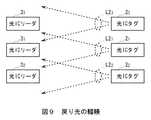
次に、上述した光IDリーダ31における制御回路30の情報抽出処理手順を、図8に示すフローチャートを用いて説明する。但し、ここでは、光IDリーダ31は、光IDタグ21〜2m(図1)のうち光IDタグ21に向けられている、つまり光IDリーダ31による識別情報の読取対象が光IDタグ21とされているものとする。(4) information extraction process Next, the information extraction processing procedure of the control circuit 30 in the optical ID reader 31 described above will be described with reference to the flowchart shown in FIG. However, here, the optical ID reader3 1 is directed to among light ID tag2 1
また、図9に示すように、光IDタグ21に近接して例えば光IDタグ22及び光IDタグ23が存在しており、これら光IDタグ22、23に対して他の光IDリーダ32、33が光IDリーダ31と同じような入射角からその光IDタグ22、23の識別情報の読み取りを行っている状況下にあるものとする。Further, as shown in FIG. 9, which is close to the optical ID tag2 1 example optical ID tag2 2 and the optical ID tag2 3 exist, other for these
制御回路30は、入力部31から識別情報の読み取り命令を受けると、この情報抽出処理手順をステップSP10において開始し、続くステップSP11において、乱数を発生するように乱数発生器51(図7)を制御するとともに、該乱数に応ずる発信周波数の信号を放射するように信号発信部52(図7)を制御し、このとき発生された乱数に応ずる発信周波数の光ビームL1(図6)をLED54(図7)から放射させる。 When receiving the identification information reading command from the
この光ビームL1は、光IDタグ21に照射され、その光IDタグ21に保持された識別情報が重畳された反射光L21(図9)として、該光IDタグ21から放射されることになる。このとき、図9に示したように、反射光L21には、他の光IDリーダ32、33に対して光IDタグ22、23から到来する反射光L22、L23が輻輳することになり、この結果、光IDリーダ31には、他の反射光L22、L23が輻輳した状態で反射光L21が到来することとなる。The light beam L1 is irradiated to the optical ID tag2 1, As optical ID tag2 1 identification information held in the superimposed reflected light L21 (FIG. 9), it is emitted from the optical ID tag2 1 Will be. At this time, as shown in FIG. 9, the reflected light L21 includes reflected light L22 and L23 coming from the
制御回路30は、ステップSP12に進んで、ステップSP11で放射した方向から到来する反射光L21を光電変換し、続くステップSP13において、該光電変換結果に基づいて、ステップSP11で放射した光ビームL1の発信周波数の信号成分から、その信号成分に重畳された識別情報を抽出するように受信処理部42(図7)を制御する。The control circuit 30 proceeds to step
そして制御回路30は、次のステップSP14において、抽出した識別情報の内容を通知するように出力部32を制御した後、ステップSP15に進んでこの情報抽出処理手順を終了する。 Then, in the next step SP14, the control circuit 30 controls the
このように制御回路30は、乱数に応ずる発信周波数の光ビームL11を放射させ、その反射光L21の受光結果のうち該発信周波数の信号成分から識別情報を抽出することによって、反射光L21に対して他の反射光L22、L23が輻輳する状態でも、読取対象である光IDタグ21に記憶された識別情報を忠実に取得し、これを通知することができるようになされている。Thus control circuit 30, a light beam L11 of the oscillation frequency of meeting the random number is radiated, by extracting the identification information from the signal component of the oscillation frequency of the reflected light L21 of the light receiving result, the reflected light L2Even when the other reflected lights L22 and L23 are congested with respect to1 , the identification information stored in the
(5)動作及び効果
以上の構成において、この光通信システム1の光IDリーダ3jは、読取操作に応じて乱数を発生し、その乱数に対して固有の発信周波数の光をLED54(図7)から放射させる。(5) Operation and Effect In the above configuration, the optical ID reader 3j of the
そして光IDリーダ3jは、このLED54から所定の光IDタグ2iに放射され、該光IDタグ2iによってその放射方向に反射され、かつ識別情報に基づいて変調された反射光をPD55(図7)を介して光電変換し、この光電変換された結果得られる信号から、発信周波数の信号成分をBPF57(図7)を介して抽出し、その信号成分を復調回路58(図7)を介して復調する。 Then, the optical ID reader 3j emits the reflected light emitted from the
したがって、この光IDリーダ3jは、照射対象となった光IDタグ21(図9)から戻り光として放射される反射光に対して、他の光IDタグ22、23(図9)から放射される反射光が輻輳した状態であったとしても、照射対象となった光IDタグ21から戻り光として放射される反射光に重畳される識別情報を抽出することができる。Therefore, the optical ID reader 3j uses the other
これによりこの光通信システム1では、例えば電車の中吊り広告に光IDタグ2iが設けられており、その光IDタグ2iに対して、複数のユーザが同時に、自己の光IDリーダ3jを用いて光IDタグ2iに保持された識別情報の読み取りを行った場合等、光IDタグ21に近接して他の光ICタ22、23グがあり、かつその他の光IDタグ22、23に対して同じような入射角から光が照射された状況下にあったとしても、読取対象とされる光IDタグ21に保持された識別情報をその光IDリーダ31が読み取ることが可能となる。この結果、光通信システム1では、光IDタグ2iにおける配置の制約を低減することが可能となる。Thereby, in this
以上の構成によれば、光IDタグ2iの配置状態や、該光IDタグ2iに対する光ICリーダの読取状況にかかわらず、識別情報を適切に伝達させ得る光通信システム1を実現できる。 According to the above configuration, it is possible to realize the
本発明は、物品を識別する、あるいは、物品を管理する分野に利用可能である。 The present invention can be used in the field of identifying an article or managing an article.
1……光通信システム、21〜2m……光IDタグ、31〜3n……光IDリーダ、13……反射量変換部、21……光学ユニット、21a……反射板、21b……LCD、21c……偏向板、22……変調回路、30……制御回路、31……情報抽出部、51……乱数発生器、52……信号発生部、54……LED、55……PD、56……検波部、57……BPF、58……復調回路。1 ......
Claims (6)
Translated fromJapanese上記光IDタグは、
上記識別情報を保持する保持手段と、
照射される光をその入射方向に反射させる反射手段と、
反射された反射光を、上記保持手段に保持された上記識別情報に基づいて変調する変調手段と
を具え、
上記光IDリーダは、
乱数を発生する乱数発生手段と、
上記乱数に対して固有の発信周波数の光を放射する放射手段と、
放射方向から到来する上記反射光を光電変換する光電変換手段と、
上記光電変換手段により光電変換された結果得られる信号から、上記発信周波数の信号成分を抽出する抽出手段と、
上記信号成分を復調する復調手段と
を具えることを特徴とする光通信システム。An optical communication system for communicating identification information between an optical ID tag and an optical ID reader using light as a communication medium,
The optical ID tag is
Holding means for holding the identification information;
Reflecting means for reflecting the irradiated light in its incident direction;
Modulation means for modulating the reflected light reflected based on the identification information held in the holding means,
The optical ID reader is
Random number generating means for generating a random number;
Radiating means for emitting light having a specific transmission frequency with respect to the random number;
Photoelectric conversion means for photoelectrically converting the reflected light coming from the radiation direction;
Extraction means for extracting a signal component of the transmission frequency from a signal obtained as a result of photoelectric conversion by the photoelectric conversion means;
An optical communication system comprising: demodulation means for demodulating the signal component.
乱数を発生する乱数発生手段と、
上記乱数に対して固有の発信周波数の光を放射する放射手段と、
上記放射手段から上記光IDタグに放射され、該光IDタグによってその放射方向に反射され、かつ上記識別情報に基づいて変調された反射光を光電変換する光電変換手段と、
上記光電変換手段により光電変換された結果得られる信号から、上記発信周波数の信号成分を抽出する抽出手段と、
上記信号成分を復調する復調手段と
を具えることを特徴とする光IDリーダ。An optical ID reader that communicates with an optical ID tag holding identification information using light as a communication medium,
Random number generating means for generating a random number;
Radiating means for emitting light having a specific transmission frequency with respect to the random number;
Photoelectric conversion means for photoelectrically converting reflected light radiated from the radiation means to the optical ID tag, reflected by the optical ID tag in the radiation direction, and modulated based on the identification information;
Extraction means for extracting a signal component of the transmission frequency from a signal obtained as a result of photoelectric conversion by the photoelectric conversion means;
An optical ID reader comprising: demodulation means for demodulating the signal component.
上記放射手段から近接する複数の上記光IDタグのうち任意の光IDタグに放射され、その光IDタグからの上記反射光を光電変換する
ことを特徴とする請求項2に記載の光IDリーダ。The photoelectric conversion means is
3. The optical ID reader according to claim 2, wherein the optical ID reader is radiated to an arbitrary optical ID tag among the plurality of optical ID tags adjacent to the radiating unit and photoelectrically converts the reflected light from the optical ID tag. .
読取操作に応じて入力手段から入力される命令を受けるごとに上記乱数を発生する
ことを特徴とする請求項2に記載の光IDリーダ。The random number generating means is
The optical ID reader according to claim 2, wherein the random number is generated every time a command input from an input unit is received in response to a reading operation.
をさらに具えることを特徴とする請求項2に記載の光IDリーダ。The optical ID reader according to claim 2, further comprising notification means for notifying the identification information obtained as a result of demodulation by the demodulation means.
乱数発生手段から乱数を発生させる第1のステップと、
上記乱数に対して固有の発信周波数の光を放射手段から放射させる第2のステップと、
上記放射手段から上記光IDタグに放射され、該光IDタグによってその放射方向に反射され、かつ上記識別情報に基づいて変調された反射光に対する光電変換結果として得られる信号から、上記発信周波数の信号成分を抽出手段に抽出させる第3のステップと、
上記信号成分を復調手段に復調させる第4のステップと
を具えることを特徴とする情報読取方法。An information reading method for reading identification information held in an optical ID tag using light as a communication medium,
A first step of generating a random number from the random number generating means;
A second step of emitting light having a transmission frequency specific to the random number from the radiation means;
From the signal obtained as a photoelectric conversion result with respect to the reflected light radiated from the radiating means to the optical ID tag, reflected in the radiation direction by the optical ID tag, and modulated based on the identification information, the transmission frequency A third step of causing the extraction means to extract the signal component;
And a fourth step of demodulating the signal component by a demodulating means.
Priority Applications (5)
| Application Number | Priority Date | Filing Date | Title |
|---|---|---|---|
| JP2006089009AJP4577577B2 (en) | 2006-03-28 | 2006-03-28 | Optical communication system |
| US11/716,713US7606451B2 (en) | 2006-03-28 | 2007-03-12 | Optical communication system, optical reader, and method of reading information |
| CN2007100918649ACN101046842B (en) | 2006-03-28 | 2007-03-28 | Optical communication system, optical reader, and method of reading information |
| EP07105102AEP1840792B1 (en) | 2006-03-28 | 2007-03-28 | Optical communication system, optical reader, and method of reading information |
| DE602007006360TDE602007006360D1 (en) | 2006-03-28 | 2007-03-28 | Optical communication system, optical reader and information reading method |
Applications Claiming Priority (1)
| Application Number | Priority Date | Filing Date | Title |
|---|---|---|---|
| JP2006089009AJP4577577B2 (en) | 2006-03-28 | 2006-03-28 | Optical communication system |
Publications (2)
| Publication Number | Publication Date |
|---|---|
| JP2007266974Atrue JP2007266974A (en) | 2007-10-11 |
| JP4577577B2 JP4577577B2 (en) | 2010-11-10 |
Family
ID=38157807
Family Applications (1)
| Application Number | Title | Priority Date | Filing Date |
|---|---|---|---|
| JP2006089009AExpired - Fee RelatedJP4577577B2 (en) | 2006-03-28 | 2006-03-28 | Optical communication system |
Country Status (5)
| Country | Link |
|---|---|
| US (1) | US7606451B2 (en) |
| EP (1) | EP1840792B1 (en) |
| JP (1) | JP4577577B2 (en) |
| CN (1) | CN101046842B (en) |
| DE (1) | DE602007006360D1 (en) |
Cited By (38)
| Publication number | Priority date | Publication date | Assignee | Title |
|---|---|---|---|---|
| WO2010027459A3 (en)* | 2008-09-05 | 2010-05-14 | Firefly Green Technologies Inc. | Optical communication device, method and system |
| US8179787B2 (en) | 2009-01-27 | 2012-05-15 | Smsc Holding S.A.R.L. | Fault tolerant network utilizing bi-directional point-to-point communications links between nodes |
| US8456092B2 (en) | 2008-09-05 | 2013-06-04 | Ketra, Inc. | Broad spectrum light source calibration systems and related methods |
| US8471496B2 (en) | 2008-09-05 | 2013-06-25 | Ketra, Inc. | LED calibration systems and related methods |
| US8521035B2 (en) | 2008-09-05 | 2013-08-27 | Ketra, Inc. | Systems and methods for visible light communication |
| US8674913B2 (en) | 2008-09-05 | 2014-03-18 | Ketra, Inc. | LED transceiver front end circuitry and related methods |
| US8749172B2 (en) | 2011-07-08 | 2014-06-10 | Ketra, Inc. | Luminance control for illumination devices |
| US8773336B2 (en) | 2008-09-05 | 2014-07-08 | Ketra, Inc. | Illumination devices and related systems and methods |
| US9146028B2 (en) | 2013-12-05 | 2015-09-29 | Ketra, Inc. | Linear LED illumination device with improved rotational hinge |
| US9155155B1 (en) | 2013-08-20 | 2015-10-06 | Ketra, Inc. | Overlapping measurement sequences for interference-resistant compensation in light emitting diode devices |
| US9237612B1 (en) | 2015-01-26 | 2016-01-12 | Ketra, Inc. | Illumination device and method for determining a target lumens that can be safely produced by an illumination device at a present temperature |
| US9237623B1 (en) | 2015-01-26 | 2016-01-12 | Ketra, Inc. | Illumination device and method for determining a maximum lumens that can be safely produced by the illumination device to achieve a target chromaticity |
| US9237620B1 (en) | 2013-08-20 | 2016-01-12 | Ketra, Inc. | Illumination device and temperature compensation method |
| US9247605B1 (en) | 2013-08-20 | 2016-01-26 | Ketra, Inc. | Interference-resistant compensation for illumination devices |
| US9276766B2 (en) | 2008-09-05 | 2016-03-01 | Ketra, Inc. | Display calibration systems and related methods |
| US9332598B1 (en) | 2013-08-20 | 2016-05-03 | Ketra, Inc. | Interference-resistant compensation for illumination devices having multiple emitter modules |
| US9345097B1 (en) | 2013-08-20 | 2016-05-17 | Ketra, Inc. | Interference-resistant compensation for illumination devices using multiple series of measurement intervals |
| US9360174B2 (en) | 2013-12-05 | 2016-06-07 | Ketra, Inc. | Linear LED illumination device with improved color mixing |
| US9386668B2 (en) | 2010-09-30 | 2016-07-05 | Ketra, Inc. | Lighting control system |
| US9392660B2 (en) | 2014-08-28 | 2016-07-12 | Ketra, Inc. | LED illumination device and calibration method for accurately characterizing the emission LEDs and photodetector(s) included within the LED illumination device |
| US9392663B2 (en) | 2014-06-25 | 2016-07-12 | Ketra, Inc. | Illumination device and method for controlling an illumination device over changes in drive current and temperature |
| US9485813B1 (en) | 2015-01-26 | 2016-11-01 | Ketra, Inc. | Illumination device and method for avoiding an over-power or over-current condition in a power converter |
| US9510416B2 (en) | 2014-08-28 | 2016-11-29 | Ketra, Inc. | LED illumination device and method for accurately controlling the intensity and color point of the illumination device over time |
| US9509525B2 (en) | 2008-09-05 | 2016-11-29 | Ketra, Inc. | Intelligent illumination device |
| US9557214B2 (en) | 2014-06-25 | 2017-01-31 | Ketra, Inc. | Illumination device and method for calibrating an illumination device over changes in temperature, drive current, and time |
| US9578724B1 (en) | 2013-08-20 | 2017-02-21 | Ketra, Inc. | Illumination device and method for avoiding flicker |
| US9651632B1 (en) | 2013-08-20 | 2017-05-16 | Ketra, Inc. | Illumination device and temperature calibration method |
| US9736903B2 (en) | 2014-06-25 | 2017-08-15 | Ketra, Inc. | Illumination device and method for calibrating and controlling an illumination device comprising a phosphor converted LED |
| US9736895B1 (en) | 2013-10-03 | 2017-08-15 | Ketra, Inc. | Color mixing optics for LED illumination device |
| US9769899B2 (en) | 2014-06-25 | 2017-09-19 | Ketra, Inc. | Illumination device and age compensation method |
| US10161786B2 (en) | 2014-06-25 | 2018-12-25 | Lutron Ketra, Llc | Emitter module for an LED illumination device |
| JP2019503478A (en)* | 2016-01-14 | 2019-02-07 | シンテフ ティティオー アクティーゼルスカブ | Semi-passive transponder |
| US10210750B2 (en) | 2011-09-13 | 2019-02-19 | Lutron Electronics Co., Inc. | System and method of extending the communication range in a visible light communication system |
| USRE48955E1 (en) | 2013-08-20 | 2022-03-01 | Lutron Technology Company Llc | Interference-resistant compensation for illumination devices having multiple emitter modules |
| USRE48956E1 (en) | 2013-08-20 | 2022-03-01 | Lutron Technology Company Llc | Interference-resistant compensation for illumination devices using multiple series of measurement intervals |
| US11272599B1 (en) | 2018-06-22 | 2022-03-08 | Lutron Technology Company Llc | Calibration procedure for a light-emitting diode light source |
| USRE49454E1 (en) | 2010-09-30 | 2023-03-07 | Lutron Technology Company Llc | Lighting control system |
| USRE50468E1 (en) | 2008-09-05 | 2025-06-24 | Lutron Technology Company Llc | Intelligent illumination device |
Families Citing this family (13)
| Publication number | Priority date | Publication date | Assignee | Title |
|---|---|---|---|---|
| JP2010034952A (en)* | 2008-07-30 | 2010-02-12 | Toshiba Corp | Visible light communication system, and visible light communication method |
| DE102011050389B4 (en) | 2011-05-16 | 2021-09-02 | Presens - Precision Sensing Gmbh | Sensor unit and measurement method |
| WO2013107039A1 (en)* | 2012-01-20 | 2013-07-25 | Chin To | System and method for identifying object |
| CN103295054B (en)* | 2012-02-29 | 2015-08-19 | 深圳光启创新技术有限公司 | A kind of photon label, recognition device and system |
| CN103903041A (en)* | 2012-12-28 | 2014-07-02 | 北京北大千方科技有限公司 | Photoelectronic label, photoelectronic label reader-writer and method for reading and writing photoelectronic label |
| US9937124B2 (en) | 2014-09-11 | 2018-04-10 | International Business Machines Corporation | Microchip substance delivery devices having low-power electromechanical release mechanisms |
| CN104715272B (en)* | 2015-03-30 | 2017-10-20 | 江苏物联网研究发展中心 | Label and reading and writing device system are modulated using light as the retroreflection of medium |
| US9734371B2 (en) | 2015-03-31 | 2017-08-15 | International Business Machines Corporation | Hybrid tag for radio frequency identification system |
| US10881788B2 (en) | 2015-10-30 | 2021-01-05 | International Business Machines Corporation | Delivery device including reactive material for programmable discrete delivery of a substance |
| CN108241885A (en)* | 2016-12-27 | 2018-07-03 | 中兴通讯股份有限公司 | A kind of passive photoelectric label |
| US10438105B2 (en)* | 2017-06-27 | 2019-10-08 | Western Digital Technologies, Inc. | Electronic label |
| CN109039439A (en)* | 2018-07-02 | 2018-12-18 | 曾昭雄 | Communication means, device and terminal |
| GB2626208B (en)* | 2023-06-30 | 2025-06-04 | Quantum Base Ltd | A method of authenticating an optically readable security element |
Citations (6)
| Publication number | Priority date | Publication date | Assignee | Title |
|---|---|---|---|---|
| JPH01276086A (en)* | 1988-04-28 | 1989-11-06 | Yamatake Honeywell Co Ltd | Reflection type photoelectric detector |
| JPH0341414A (en)* | 1989-07-07 | 1991-02-21 | Opt Kk | Identification card |
| JP2000004183A (en)* | 1998-06-12 | 2000-01-07 | Mitsubishi Electric Corp | Microwave data carrier system with passive modulation |
| JP2000101578A (en)* | 1998-09-21 | 2000-04-07 | Matsushita Electric Ind Co Ltd | Wireless network system |
| JP2003060516A (en)* | 2001-08-15 | 2003-02-28 | Yokohama Rubber Co Ltd:The | Transmitter and radio transmission system |
| JP2006011948A (en)* | 2004-06-28 | 2006-01-12 | Ntt Communications Kk | Directional optical ID device |
Family Cites Families (5)
| Publication number | Priority date | Publication date | Assignee | Title |
|---|---|---|---|---|
| US4916296A (en) | 1987-10-29 | 1990-04-10 | Jerry R. Iggulden | Light modulating smart card |
| IL96764A (en) | 1990-12-23 | 1994-07-31 | Zuta Marc | Smart card integrated in a wristwatch and having logic unit controlling the automatic identification process and the data transfer |
| US6618117B2 (en)* | 1997-07-12 | 2003-09-09 | Silverbrook Research Pty Ltd | Image sensing apparatus including a microcontroller |
| US6970916B1 (en)* | 1998-09-11 | 2005-11-29 | L. V. Partners, L.P. | Method for conducting a contest using a network |
| US7308207B2 (en) | 2003-11-17 | 2007-12-11 | Raytheon Company | Method for identifying an interrogated object using a dynamic optical tag identification system |
- 2006
- 2006-03-28JPJP2006089009Apatent/JP4577577B2/ennot_activeExpired - Fee Related
- 2007
- 2007-03-12USUS11/716,713patent/US7606451B2/ennot_activeExpired - Fee Related
- 2007-03-28CNCN2007100918649Apatent/CN101046842B/ennot_activeExpired - Fee Related
- 2007-03-28EPEP07105102Apatent/EP1840792B1/ennot_activeExpired - Fee Related
- 2007-03-28DEDE602007006360Tpatent/DE602007006360D1/enactiveActive
Patent Citations (6)
| Publication number | Priority date | Publication date | Assignee | Title |
|---|---|---|---|---|
| JPH01276086A (en)* | 1988-04-28 | 1989-11-06 | Yamatake Honeywell Co Ltd | Reflection type photoelectric detector |
| JPH0341414A (en)* | 1989-07-07 | 1991-02-21 | Opt Kk | Identification card |
| JP2000004183A (en)* | 1998-06-12 | 2000-01-07 | Mitsubishi Electric Corp | Microwave data carrier system with passive modulation |
| JP2000101578A (en)* | 1998-09-21 | 2000-04-07 | Matsushita Electric Ind Co Ltd | Wireless network system |
| JP2003060516A (en)* | 2001-08-15 | 2003-02-28 | Yokohama Rubber Co Ltd:The | Transmitter and radio transmission system |
| JP2006011948A (en)* | 2004-06-28 | 2006-01-12 | Ntt Communications Kk | Directional optical ID device |
Cited By (67)
| Publication number | Priority date | Publication date | Assignee | Title |
|---|---|---|---|---|
| US8886047B2 (en) | 2008-09-05 | 2014-11-11 | Ketra, Inc. | Optical communication device, method and system |
| US10847026B2 (en) | 2008-09-05 | 2020-11-24 | Lutron Ketra, Llc | Visible light communication system and method |
| US8456092B2 (en) | 2008-09-05 | 2013-06-04 | Ketra, Inc. | Broad spectrum light source calibration systems and related methods |
| US9509525B2 (en) | 2008-09-05 | 2016-11-29 | Ketra, Inc. | Intelligent illumination device |
| US8521035B2 (en) | 2008-09-05 | 2013-08-27 | Ketra, Inc. | Systems and methods for visible light communication |
| US8674913B2 (en) | 2008-09-05 | 2014-03-18 | Ketra, Inc. | LED transceiver front end circuitry and related methods |
| US9295112B2 (en) | 2008-09-05 | 2016-03-22 | Ketra, Inc. | Illumination devices and related systems and methods |
| US8773336B2 (en) | 2008-09-05 | 2014-07-08 | Ketra, Inc. | Illumination devices and related systems and methods |
| US9276766B2 (en) | 2008-09-05 | 2016-03-01 | Ketra, Inc. | Display calibration systems and related methods |
| WO2010027459A3 (en)* | 2008-09-05 | 2010-05-14 | Firefly Green Technologies Inc. | Optical communication device, method and system |
| US8471496B2 (en) | 2008-09-05 | 2013-06-25 | Ketra, Inc. | LED calibration systems and related methods |
| USRE50468E1 (en) | 2008-09-05 | 2025-06-24 | Lutron Technology Company Llc | Intelligent illumination device |
| US8179787B2 (en) | 2009-01-27 | 2012-05-15 | Smsc Holding S.A.R.L. | Fault tolerant network utilizing bi-directional point-to-point communications links between nodes |
| USRE49454E1 (en) | 2010-09-30 | 2023-03-07 | Lutron Technology Company Llc | Lighting control system |
| US9386668B2 (en) | 2010-09-30 | 2016-07-05 | Ketra, Inc. | Lighting control system |
| US8749172B2 (en) | 2011-07-08 | 2014-06-10 | Ketra, Inc. | Luminance control for illumination devices |
| US10210750B2 (en) | 2011-09-13 | 2019-02-19 | Lutron Electronics Co., Inc. | System and method of extending the communication range in a visible light communication system |
| US11915581B2 (en) | 2011-09-13 | 2024-02-27 | Lutron Technology Company, LLC | Visible light communication system and method |
| US11210934B2 (en) | 2011-09-13 | 2021-12-28 | Lutron Technology Company Llc | Visible light communication system and method |
| US9155155B1 (en) | 2013-08-20 | 2015-10-06 | Ketra, Inc. | Overlapping measurement sequences for interference-resistant compensation in light emitting diode devices |
| USRE49705E1 (en) | 2013-08-20 | 2023-10-17 | Lutron Technology Company Llc | Interference-resistant compensation for illumination devices using multiple series of measurement intervals |
| USRE48956E1 (en) | 2013-08-20 | 2022-03-01 | Lutron Technology Company Llc | Interference-resistant compensation for illumination devices using multiple series of measurement intervals |
| USRE48955E1 (en) | 2013-08-20 | 2022-03-01 | Lutron Technology Company Llc | Interference-resistant compensation for illumination devices having multiple emitter modules |
| USRE49421E1 (en) | 2013-08-20 | 2023-02-14 | Lutron Technology Company Llc | Illumination device and method for avoiding flicker |
| USRE50018E1 (en) | 2013-08-20 | 2024-06-18 | Lutron Technology Company Llc | Interference-resistant compensation for illumination devices having multiple emitter modules |
| US9345097B1 (en) | 2013-08-20 | 2016-05-17 | Ketra, Inc. | Interference-resistant compensation for illumination devices using multiple series of measurement intervals |
| US9332598B1 (en) | 2013-08-20 | 2016-05-03 | Ketra, Inc. | Interference-resistant compensation for illumination devices having multiple emitter modules |
| US9578724B1 (en) | 2013-08-20 | 2017-02-21 | Ketra, Inc. | Illumination device and method for avoiding flicker |
| US9651632B1 (en) | 2013-08-20 | 2017-05-16 | Ketra, Inc. | Illumination device and temperature calibration method |
| US9237620B1 (en) | 2013-08-20 | 2016-01-12 | Ketra, Inc. | Illumination device and temperature compensation method |
| US9247605B1 (en) | 2013-08-20 | 2016-01-26 | Ketra, Inc. | Interference-resistant compensation for illumination devices |
| US9736895B1 (en) | 2013-10-03 | 2017-08-15 | Ketra, Inc. | Color mixing optics for LED illumination device |
| US11662077B2 (en) | 2013-10-03 | 2023-05-30 | Lutron Technology Company Llc | Color mixing optics for LED illumination device |
| US12072091B2 (en) | 2013-10-03 | 2024-08-27 | Lutron Technology Company Llc | Color mixing optics for LED illumination device |
| US11326761B2 (en) | 2013-10-03 | 2022-05-10 | Lutron Technology Company Llc | Color mixing optics for LED illumination device |
| US12292184B2 (en) | 2013-10-03 | 2025-05-06 | Lutron Technology Company Llc | Color mixing optics for LED illumination device |
| US9360174B2 (en) | 2013-12-05 | 2016-06-07 | Ketra, Inc. | Linear LED illumination device with improved color mixing |
| US9668314B2 (en) | 2013-12-05 | 2017-05-30 | Ketra, Inc. | Linear LED illumination device with improved color mixing |
| USRE50562E1 (en) | 2013-12-05 | 2025-08-26 | Lutron Technology Company Llc | Linear LED illumination device with improved color mixing |
| USRE50470E1 (en) | 2013-12-05 | 2025-06-24 | Lutron Technology Company Llc | Linear LED illumination device with improved color mixing |
| US9146028B2 (en) | 2013-12-05 | 2015-09-29 | Ketra, Inc. | Linear LED illumination device with improved rotational hinge |
| USRE48922E1 (en) | 2013-12-05 | 2022-02-01 | Lutron Technology Company Llc | Linear LED illumination device with improved color mixing |
| US9769899B2 (en) | 2014-06-25 | 2017-09-19 | Ketra, Inc. | Illumination device and age compensation method |
| US12292326B2 (en) | 2014-06-25 | 2025-05-06 | Lutron Technology Company Llc | Emitter module for an LED illumination device |
| US11243112B2 (en) | 2014-06-25 | 2022-02-08 | Lutron Technology Company Llc | Emitter module for an LED illumination device |
| US11252805B2 (en) | 2014-06-25 | 2022-02-15 | Lutron Technology Company Llc | Illumination device and method for calibrating an illumination device over changes in temperature, drive current, and time |
| US9392663B2 (en) | 2014-06-25 | 2016-07-12 | Ketra, Inc. | Illumination device and method for controlling an illumination device over changes in drive current and temperature |
| US10605652B2 (en) | 2014-06-25 | 2020-03-31 | Lutron Ketra, Llc | Emitter module for an LED illumination device |
| US12050126B2 (en) | 2014-06-25 | 2024-07-30 | Lutron Technology Company Llc | Emitter module for an LED illumination device |
| US12052807B2 (en) | 2014-06-25 | 2024-07-30 | Lutron Technology Company Llc | Illumination device and method for calibrating an illumination device over changes in temperature, drive current, and time |
| US10595372B2 (en) | 2014-06-25 | 2020-03-17 | Lutron Ketra, Llc | Illumination device and method for calibrating an illumination device over changes in temperature, drive current, and time |
| US9557214B2 (en) | 2014-06-25 | 2017-01-31 | Ketra, Inc. | Illumination device and method for calibrating an illumination device over changes in temperature, drive current, and time |
| US9736903B2 (en) | 2014-06-25 | 2017-08-15 | Ketra, Inc. | Illumination device and method for calibrating and controlling an illumination device comprising a phosphor converted LED |
| US10161786B2 (en) | 2014-06-25 | 2018-12-25 | Lutron Ketra, Llc | Emitter module for an LED illumination device |
| US9392660B2 (en) | 2014-08-28 | 2016-07-12 | Ketra, Inc. | LED illumination device and calibration method for accurately characterizing the emission LEDs and photodetector(s) included within the LED illumination device |
| US9510416B2 (en) | 2014-08-28 | 2016-11-29 | Ketra, Inc. | LED illumination device and method for accurately controlling the intensity and color point of the illumination device over time |
| USRE49246E1 (en) | 2014-08-28 | 2022-10-11 | Lutron Technology Company Llc | LED illumination device and method for accurately controlling the intensity and color point of the illumination device over time |
| USRE49479E1 (en) | 2014-08-28 | 2023-03-28 | Lutron Technology Company Llc | LED illumination device and calibration method for accurately characterizing the emission LEDs and photodetector(s) included within the LED illumination device |
| USRE49137E1 (en) | 2015-01-26 | 2022-07-12 | Lutron Technology Company Llc | Illumination device and method for avoiding an over-power or over-current condition in a power converter |
| US9485813B1 (en) | 2015-01-26 | 2016-11-01 | Ketra, Inc. | Illumination device and method for avoiding an over-power or over-current condition in a power converter |
| US9237623B1 (en) | 2015-01-26 | 2016-01-12 | Ketra, Inc. | Illumination device and method for determining a maximum lumens that can be safely produced by the illumination device to achieve a target chromaticity |
| US9237612B1 (en) | 2015-01-26 | 2016-01-12 | Ketra, Inc. | Illumination device and method for determining a target lumens that can be safely produced by an illumination device at a present temperature |
| USRE50612E1 (en) | 2015-01-26 | 2025-09-30 | Lutron Technology Company Llc | Illumination device and method for avoiding an over-power or over-current condition in a power converter |
| JP2019503478A (en)* | 2016-01-14 | 2019-02-07 | シンテフ ティティオー アクティーゼルスカブ | Semi-passive transponder |
| US10948594B2 (en) | 2016-01-14 | 2021-03-16 | Sintef Tto As | Semi-passive transponder |
| US11272599B1 (en) | 2018-06-22 | 2022-03-08 | Lutron Technology Company Llc | Calibration procedure for a light-emitting diode light source |
| US12302466B1 (en) | 2018-06-22 | 2025-05-13 | Lutron Technology Company Llc | Calibration procedure for a light-emitting diode light source |
Also Published As
| Publication number | Publication date |
|---|---|
| EP1840792B1 (en) | 2010-05-12 |
| DE602007006360D1 (en) | 2010-06-24 |
| EP1840792A1 (en) | 2007-10-03 |
| JP4577577B2 (en) | 2010-11-10 |
| US20070230322A1 (en) | 2007-10-04 |
| CN101046842A (en) | 2007-10-03 |
| CN101046842B (en) | 2010-10-27 |
| US7606451B2 (en) | 2009-10-20 |
Similar Documents
| Publication | Publication Date | Title |
|---|---|---|
| JP4577577B2 (en) | Optical communication system | |
| US8184007B2 (en) | Wireless tag reader/writer | |
| RU2020127281A (en) | INTERACTIVE SYSTEMS AND METHODS WITH FEEDBACK DEVICES | |
| JP5653425B2 (en) | RFID system | |
| JP2021510957A5 (en) | ||
| US20120229259A1 (en) | Stochastic communication protocol method and system for radio frequency identification (rfid) tags based on coalition formation, such as for tag-to-tag communication | |
| US20080030305A1 (en) | Systems and Methods for Using a Tag | |
| JPH04140685A (en) | Response device used in mobile object identification system | |
| KR20080082698A (en) | Optical Identification Tags, Readers & Systems | |
| CN1980084A (en) | Position locator for locating position of rfid tag | |
| CN107492238A (en) | One kind finds article system and its method | |
| CN105404909A (en) | RFID book management apparatus | |
| JP2005216044A (en) | Non-contact ic card and holder for non-contact ic card | |
| WO2010134154A1 (en) | Optical communication system and optical communication method | |
| US20080100452A1 (en) | RFID tag with barcode symbology antenna configuration | |
| JP2005108112A (en) | Tag information reading method and apparatus | |
| JP2005005876A (en) | Wireless data carrier recognition device | |
| CA3096574A1 (en) | Self-powered semi-active electronic tag with autonomous processing capability and its communication procedure | |
| JP2007282045A (en) | Optical communication system, optical id tag and information transmitting method | |
| JP5065385B2 (en) | Transponder and system having said transponder | |
| JP2008257489A (en) | Non-contact ic tag system | |
| JP2005100357A (en) | Non-contact type data carrier, its terminal equipment and access system | |
| KR102125357B1 (en) | System and method for bidirectional visible light communication without external power supply based on backscattering of modulated light | |
| CN103955723A (en) | Data processing system in environment with radio frequency identification tags densely arranged | |
| JP4664012B2 (en) | Directional optical ID device and optical ID tag |
Legal Events
| Date | Code | Title | Description |
|---|---|---|---|
| A977 | Report on retrieval | Free format text:JAPANESE INTERMEDIATE CODE: A971007 Effective date:20090427 | |
| A131 | Notification of reasons for refusal | Free format text:JAPANESE INTERMEDIATE CODE: A131 Effective date:20090507 | |
| A521 | Written amendment | Free format text:JAPANESE INTERMEDIATE CODE: A523 Effective date:20090626 | |
| A131 | Notification of reasons for refusal | Free format text:JAPANESE INTERMEDIATE CODE: A131 Effective date:20100121 | |
| A521 | Written amendment | Free format text:JAPANESE INTERMEDIATE CODE: A523 Effective date:20100217 | |
| TRDD | Decision of grant or rejection written | ||
| A01 | Written decision to grant a patent or to grant a registration (utility model) | Free format text:JAPANESE INTERMEDIATE CODE: A01 Effective date:20100729 | |
| A01 | Written decision to grant a patent or to grant a registration (utility model) | Free format text:JAPANESE INTERMEDIATE CODE: A01 | |
| A61 | First payment of annual fees (during grant procedure) | Free format text:JAPANESE INTERMEDIATE CODE: A61 Effective date:20100811 | |
| FPAY | Renewal fee payment (event date is renewal date of database) | Free format text:PAYMENT UNTIL: 20130903 Year of fee payment:3 | |
| FPAY | Renewal fee payment (event date is renewal date of database) | Free format text:PAYMENT UNTIL: 20130903 Year of fee payment:3 | |
| LAPS | Cancellation because of no payment of annual fees |