JP2007266935A - Pll circuit - Google Patents
Pll circuitDownload PDFInfo
- Publication number
- JP2007266935A JP2007266935AJP2006088519AJP2006088519AJP2007266935AJP 2007266935 AJP2007266935 AJP 2007266935AJP 2006088519 AJP2006088519 AJP 2006088519AJP 2006088519 AJP2006088519 AJP 2006088519AJP 2007266935 AJP2007266935 AJP 2007266935A
- Authority
- JP
- Japan
- Prior art keywords
- charge pump
- dummy
- circuit
- signal
- current source
- Prior art date
- Legal status (The legal status is an assumption and is not a legal conclusion. Google has not performed a legal analysis and makes no representation as to the accuracy of the status listed.)
- Pending
Links
- 238000000605extractionMethods0.000claimsdescription9
- 238000001914filtrationMethods0.000claimsdescription6
- 230000010355oscillationEffects0.000claimsdescription4
- 238000004519manufacturing processMethods0.000abstractdescription8
- 238000007599dischargingMethods0.000abstract3
- 239000013256coordination polymerSubstances0.000description16
- 102100026533Cytochrome P450 1A2Human genes0.000description9
- 101000855342Homo sapiens Cytochrome P450 1A2Proteins0.000description9
- 238000010586diagramMethods0.000description7
- 230000007423decreaseEffects0.000description5
- 238000000034methodMethods0.000description5
- 230000003071parasitic effectEffects0.000description5
- 239000000758substrateSubstances0.000description5
- 238000004364calculation methodMethods0.000description4
- 230000000630rising effectEffects0.000description3
- 239000003990capacitorSubstances0.000description1
- 238000001514detection methodMethods0.000description1
- 238000005516engineering processMethods0.000description1
- 239000004065semiconductorSubstances0.000description1
Images


Classifications
- H—ELECTRICITY
- H03—ELECTRONIC CIRCUITRY
- H03L—AUTOMATIC CONTROL, STARTING, SYNCHRONISATION OR STABILISATION OF GENERATORS OF ELECTRONIC OSCILLATIONS OR PULSES
- H03L7/00—Automatic control of frequency or phase; Synchronisation
- H03L7/06—Automatic control of frequency or phase; Synchronisation using a reference signal applied to a frequency- or phase-locked loop
- H03L7/08—Details of the phase-locked loop
- H03L7/085—Details of the phase-locked loop concerning mainly the frequency- or phase-detection arrangement including the filtering or amplification of its output signal
- H03L7/087—Details of the phase-locked loop concerning mainly the frequency- or phase-detection arrangement including the filtering or amplification of its output signal using at least two phase detectors or a frequency and phase detector in the loop
- H—ELECTRICITY
- H03—ELECTRONIC CIRCUITRY
- H03L—AUTOMATIC CONTROL, STARTING, SYNCHRONISATION OR STABILISATION OF GENERATORS OF ELECTRONIC OSCILLATIONS OR PULSES
- H03L7/00—Automatic control of frequency or phase; Synchronisation
- H03L7/06—Automatic control of frequency or phase; Synchronisation using a reference signal applied to a frequency- or phase-locked loop
- H03L7/08—Details of the phase-locked loop
- H03L7/085—Details of the phase-locked loop concerning mainly the frequency- or phase-detection arrangement including the filtering or amplification of its output signal
- H03L7/089—Details of the phase-locked loop concerning mainly the frequency- or phase-detection arrangement including the filtering or amplification of its output signal the phase or frequency detector generating up-down pulses
- H03L7/0891—Details of the phase-locked loop concerning mainly the frequency- or phase-detection arrangement including the filtering or amplification of its output signal the phase or frequency detector generating up-down pulses the up-down pulses controlling source and sink current generators, e.g. a charge pump
- H03L7/0893—Details of the phase-locked loop concerning mainly the frequency- or phase-detection arrangement including the filtering or amplification of its output signal the phase or frequency detector generating up-down pulses the up-down pulses controlling source and sink current generators, e.g. a charge pump the up-down pulses controlling at least two source current generators or at least two sink current generators connected to different points in the loop
Landscapes
- Stabilization Of Oscillater, Synchronisation, Frequency Synthesizers (AREA)
Abstract
Description
Translated fromJapaneseこの発明は、主チャージポンプを含む主回路に対して、ダミーチャージポンプをを含むダミー回路を備えたPLL回路に関する。 The present invention relates to a PLL circuit including a dummy circuit including a dummy charge pump with respect to a main circuit including a main charge pump.
近年において、半導体製造技術の進歩に伴って回路素子は微細化され、これによって、LSI(Large Scale Integrated Circuit:大規模集積回路)を構成する個々のトランジスタの特性のばらつきの影響が大きくなっている。
その一つとして、周知の、主チャージポンプ(Charge Pump :以下、CPと略す)を含む主回路と、ダミーCPを含むダミー回路とからなるPLL(Phase Locked Loop : 位相追従閉ループ)回路における、主回路とダミー回路とのそれぞれの電流源の製造誤差に基づく、REF(Reference clock : 基準クロック) とFBK(Feedback clock :帰還クロック)との位相オフセットが問題になっている。In recent years, circuit elements have been miniaturized with the progress of semiconductor manufacturing technology, and this has increased the influence of variations in characteristics of individual transistors constituting an LSI (Large Scale Integrated Circuit). .
As one of them, a main PLL in a well-known PLL (Phase Locked Loop) circuit comprising a main circuit including a main charge pump (hereinafter abbreviated as CP) and a dummy circuit including a dummy CP. A phase offset between REF (Reference clock) and FBK (Feedback clock) based on the manufacturing error of each current source of the circuit and the dummy circuit is a problem.
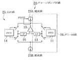
図7は、従来の主回路に対してダミー回路を備えたPLL回路を例示したのもであって、PFD(Fhase Frequency Detector:位相比較器)11と、CP12と、LF(ローパスフィルタ)13と、PFD14と、CP15と、LF16と、VCO(Voltage Controlled Oscillator : 電圧制御発振器)17と、DIV(Divider :分周器)18と、OPAMP(Operational Amplifier :演算増幅器)19とから概略構成されている。
これらのうち、PFD11,CP12,LF13からなる回路はダミー回路、PFD14,CP15,LF16からなる回路は主回路である。FIG. 7 illustrates a PLL circuit having a dummy circuit with respect to the conventional main circuit, and includes a PFD (Fhase Frequency Detector) 11, a
Among these, the circuit composed of PFD11, CP12, and LF13 is a dummy circuit, and the circuit composed of PFD14, CP15, and LF16 is a main circuit.
PFD11は、一対の入力にそれぞれ加えられる基準クロックREFの位相を比較して、回路的なアンバランス等に基づく位相差に応じてダミーアップ(UP)信号又はダミーダウン(DOWN)信号を出力する。CP12は、ダミーUP信号に応じてその出力電圧を上昇させ、ダミーDOWN信号に応じてその出力電圧を低下させる。LF13は、CP12の出力電圧の高周波成分を除去して、制御信号Vcntダミーを出力する。 The
PFD14は、一対の入力に加えられる基準クロックREFと帰還クロックFBKとの位相を比較して、位相差に応じてUP信号又はDOWN信号を出力する。CP15は、UP信号に応じてその出力電圧を上昇させ、DOWN信号に応じてその出力電圧を低下させる。LF16は、CP15の出力電圧の高周波成分を除去して、制御信号Vcntを出力する。 The
VCO17は、制御信号Vcntの電圧の大小に応じて周波数が上昇し又は低下する信号を発振する。DIV18は、VCO17の出力信号の周波数を所定の比で分周して、帰還クロックFBKとして出力する。OPAMP19は差動増幅器を形成し、ダミー回路から出力された制御信号Vcntダミーと、主回路から出力された制御信号Vcntとの大小関係に応じて、レベルが変化する制御信号PBIAS を出力する。 The
ダミー回路は、例えばLSI上において、主回路の回路配置,配線長等を模擬するように形成されている。ダミー回路のPFD11では、基準クロックREFの2入力の位相比較を行うが、両入力の配線長の違いや寄生容量の違い等に基づいて、ダミーUP信号又はダミーDOWN信号とを発生するので、これによってCP12の出力電圧が変化する。
主回路のPFD14では、基準クロックREFと帰還クロックFBKとの位相比較を行ってUP信号とDOWN信号とを発生し、これによってCP15の出力電圧が変化するが、UP信号とDOWN信号には、基準クロックREFと帰還クロックFBKとの両入力の配線長の違いや寄生容量の違い等に基づいて、ダミーUP信号とダミーDOWN信号と同じ大きさの成分を含んでいる。
そこで、OPAMP19において、ダミー回路の出力制御信号Vcntダミーと主回路の出力制御信号Vcntとの差分から演算して発生した制御信号PBIAS によってダミー回路のCP12と主回路のCP15とのそれぞれの電流源(不図示)を制御することによって、主回路のPFD14における両入力の配線長の違いや寄生容量の違い等に基づく出力誤差を除去する。The dummy circuit is formed on the LSI, for example, so as to simulate the circuit arrangement of the main circuit, the wiring length, and the like. In the
The
Therefore, in the
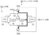
図8は、図7に示されたPLL回路における、ダミー回路のCP12と主回路のCP15との制御を説明するものである。
ダミー回路のPFD11の出力によってスイッチ(不図示)を動作させて、ダミー回路のCP12の流し込み側の電流源21Aと引き抜き側の電流源21Bとを制御することによって、CP12の出力電圧を制御し、主回路のPFD14の出力によってスイッチ(不図示)を動作させて、主回路のCP15の流し込み側の電流源22Aと引き抜き側の電流源22Bとを制御することによって、CP15の出力電圧を制御する。
そして、CP12,CP15の出力電圧をそれぞれLF13,LF16を介してフィルタリングした信号からOPAMP19によって差分を演算して発生した制御信号PBIAS によって電流源21A,21Bと22A,22Bとを動作させて、流し込み側電流源21A又は22AからCP12又はCP15へのの流入電流を制御し、CP12又はCP15から引き抜き側電流源21B又は22Bへの流出電流を制御することによって、主回路のPFD14における、2入力の配線長の違いや寄生容量の違い等に基づく出力誤差を除去するようにしている。FIG. 8 explains the control of the dummy circuit CP12 and the main circuit CP15 in the PLL circuit shown in FIG.
By operating a switch (not shown) by the output of the
Then, the
しかしながら、図7に示された従来のPLL回路では、両電流源21A,21Bと22A,22Bとに、製造誤差に基づく電流供給能力や、リーク電流の大きさ等の違いがあった場合には、これらの原因に基づく制御信号Vcntダミーと制御信号Vcntとの出力誤差を除去することができず、そのため基準クロックREFと帰還クロックFBKとの位相オフセットが発生するという問題があった。 However, in the conventional PLL circuit shown in FIG. 7, when there is a difference between the
これに対して特許文献1においては、主チャージポンプを構成する充放電手段の寄生容量や素子の非線形性が原因で発生するリーク電荷を打ち消すことが可能な、チャージポンプ型位相比較器が開示されている。特許文献1記載のチャージポンプ型位相比較器では、主チャージポンプ981が電流源973と放電手段932,942とから構成され、副チャージポンプ982が電流源974と放電手段952,962とから構成されることが記載されている(〔0023〕)。
このように、特許文献1記載の技術では、主チャージポンプ981の電流源973と、副チャージポンプ982の電流源974とは別個であって、従って、上述した従来のPLL回路における問題点は解決されていない。On the other hand,
As described above, in the technique described in
また、特許文献2においては、リファレンスリークが十分に抑圧され、かつ限界までループ帯域を広帯域に設定できるために、位相ノイズが低減化できるPLL発振器が実現可能なPLL回路が開示されている。特許文献2記載のPLL回路においては、チャージポンプ回路2を備えるPLLループに対して、位相比較器1から出力される誤差信号を電流に変換するチャージポンプ回路6を備えた回路が記載されている(〔0028〕〜〔0031〕)。この場合、チャージポンプ回路2が可変電流源回路12を備えることが記載されているが、チャージポンプ回路2とチャージポンプ回路6とは同一の構成(〔0034〕)なので、チャージポンプ回路6もまた可変電流源回路を備えている。
このように、特許文献2記載の技術では、両チャージポンプ回路の電流源は別個であって、従って、上述した従来のPLL回路における問題点は解決されていない。Further, Patent Document 2 discloses a PLL circuit capable of realizing a PLL oscillator capable of reducing phase noise since reference leak is sufficiently suppressed and the loop band can be set to a wide band to the limit. In the PLL circuit described in Patent Document 2, a circuit including a charge pump circuit 6 that converts an error signal output from the
As described above, in the technique described in Patent Document 2, the current sources of both charge pump circuits are separate, and thus the above-described problems in the conventional PLL circuit are not solved.
また、特許文献3においては、アップ信号およひダウン信号によりフィルタ容量の充放電を行うチャージポンプ回路の他に、現在の充電電圧と目標とする電圧とを比較して現在の充電電圧が低い間は、第2のチャージポンプ回路を動作させて、高速充電を行うPLL回路が開示されている。この場合、第1のチャージポンプ回路CP1と第2のチャージポンプ回路CP2とは別個の電流源に接続されている(図1〜図3参照)。
このように、特許文献3記載の技術では、第1のチャージポンプ回路CP1と第2のチャージポンプ回路CP2との電流源は別個であって、従って、上述した従来のPLL回路における問題点は解決されていない。In Patent Document 3, in addition to a charge pump circuit that charges and discharges a filter capacitor using an up signal and a down signal, the current charging voltage is compared with a target voltage, and the current charging voltage is low. In the meantime, a PLL circuit that operates the second charge pump circuit to perform high-speed charging is disclosed. In this case, the first charge pump circuit CP1 and the second charge pump circuit CP2 are connected to separate current sources (see FIGS. 1 to 3).
As described above, in the technique described in Patent Document 3, the current sources of the first charge pump circuit CP1 and the second charge pump circuit CP2 are separate, and therefore, the problem in the conventional PLL circuit described above is solved. It has not been.
また、特許文献4においては、チャージポンプ回路に対して予備のチャージポンプ回路を設けることによって、電圧の浮き上がりを抑止する基板電圧発生回路が開示されている。特許文献4には、それぞれ基板電圧を発生する複数の主チャージポンプ手段に対して、予備チャージポンプ手段を備え、電源電圧検出回路2において電源電圧を検出して、電源電圧の大きさが通常使用範囲より大きくなる場合は、休止状態にあった予備のチャージポンプ手段および駆動回路が動作して基板電圧発生回路の能力を大幅に向上させるので、基板電圧の浮き上がりを防止することができることが記載されている(第6頁右欄第3〜8行)。
このように、特許文献4記載の技術では、電源電圧の大きさが通常使用範囲より大きくなる場合は、予備のチャージポンプ手段が動作して基板電圧発生回路の能力を向上させることが記載されているだけであって、上述した従来のPLL回路における問題点の解決については特に関係がない。Further, Patent Document 4 discloses a substrate voltage generation circuit that suppresses voltage rise by providing a spare charge pump circuit for a charge pump circuit. In Patent Document 4, spare charge pump means is provided for a plurality of main charge pump means each generating a substrate voltage, the power supply voltage is detected by the power supply voltage detection circuit 2, and the magnitude of the power supply voltage is normally used. If it exceeds the range, it is described that the standby charge pump means and the drive circuit that have been in the quiescent state operate to greatly improve the capability of the substrate voltage generation circuit, so that the substrate voltage can be prevented from rising. (Page 6, right column, lines 3-8).
As described above, the technique described in Patent Document 4 describes that when the power supply voltage is larger than the normal use range, the spare charge pump unit operates to improve the capability of the substrate voltage generation circuit. However, there is no particular relationship with respect to solving the problems in the conventional PLL circuit described above.
さらに特許文献5においては、基準クロックと帰還クロックの位相オフセットを低減したPLL回路が開示されている。このPLL回路は、ダミー位相比較器16と、ダミーチャージポンプ17とを備えたダミー回路と、位相比較器11とチャージポンプ12とを備えた主回路とは同一回路構成を有している(〔0022〕)。ダミーチャージポンプ17とチャージポンプ12の構成については特に記載されていないが、図示されない電流源によって動作する従来回路のチャージポンプ32(図8参照)と同じ回路構成を有するものと解される。従ってダミーチャージポンプ17とチャージポンプ12とは別個の電流源を有している。
このように、特許文献5記載の技術では、ダミーチャージポンプ17とチャージポンプ12との電流源は別個であって、従って、上述した従来のPLL回路における問題点は解決されていない。
As described above, in the technique described in Patent Document 5, the current sources of the
従来の、ダミー位相比較器とダミーチャージポンプとを備えたダミー回路と、位相比較器とチャージポンプとを備えた主回路とを有するPLL回路においては、ダミー回路と主回路とのそれぞれの電流源を構成するトランジスタのばらつき等の製造誤差に基づく、それぞれの電流源の電流供給能力や、リーク電流の大きさの違い等の回路アンバランスがあった場合、基準クロックREFと帰還クロックFBKとに位相オフセットを生じることを避けられないという問題があった。 In a conventional PLL circuit having a dummy circuit having a dummy phase comparator and a dummy charge pump and a main circuit having a phase comparator and a charge pump, current sources of the dummy circuit and the main circuit are respectively provided. When there is a circuit imbalance such as a current supply capability of each current source or a difference in the magnitude of the leakage current based on a manufacturing error such as a variation in transistors constituting the phase, the reference clock REF and the feedback clock FBK have a phase difference. There was a problem that it was inevitable that an offset would occur.
この発明は上述の事情に鑑みてなされたものであって、ダミー位相比較器とダミーチャージポンプとを備えたダミー回路と、位相比較器とチャージポンプとを備えた主回路とを有するPLL回路において、電流源の製造誤差に基づく、基準クロックと帰還クロックとの位相オフセットを低減することを目的としている。 The present invention has been made in view of the above circumstances, and is a PLL circuit having a dummy circuit having a dummy phase comparator and a dummy charge pump, and a main circuit having a phase comparator and a charge pump. An object of the present invention is to reduce the phase offset between the reference clock and the feedback clock based on the manufacturing error of the current source.
上記課題を解決するため、請求項1記載の発明はPLL回路に係り、一対の入力にそれぞれ接続された基準クロックと帰還クロックとの位相の比較結果に応じてアップ信号又はダウン信号を出力する第1の位相比較手段と、第1のチャージポンプの出力電圧をフィルタリングする第1のローパスフィルタと、該第1のローパスフィルタの出力電圧に応じた周波数の帰還クロックを発生する電圧制御発振手段とを備えた第1の回路と、
上記第1の位相比較手段を模擬し、一対の入力にそれぞれ接続された基準クロックの位相の比較結果に応じてダミーアップ信号又はダミーダウン信号を出力する第2の位相比較手段と、上記第1のチャージポンプを模擬する第2のチャージポンプの出力電圧をフィルタリングする第2のローパスフィルタとを備えた第2の回路と、
上記第1の位相比較手段からのアップ信号又はダウン信号に応じて出力電圧が上昇し又は下降する第1のチャージポンプと、上記第1のチャージポンプを模擬し、上記第2の位相比較手段からのダミーアップ信号又はダミーダウン信号に応じて出力電圧が上昇し又は下降する第2のチャージポンプと、流し込み側と引き抜き側とからなる電流源とを備え、上記アップ信号又はダミーアップ信号によって流し込み側電流源が動作可能となり、上記ダウン信号又はダミーダウン信号によって引き抜き側電流源が動作可能となるとともに、上記第1のローパスフィルタの出力と第2のローパスフィルタの出力との差分に応じて、上記流し込み側電流源から上記第1のチャージポンプ又は第2のチャージポンプに流出する電流又は上記第1のチャージポンプ又は第2のチャージポンプから上記引き抜き側電流源に流入する電流を制御するチャージポンプ回路とを備えたことを特徴としている。In order to solve the above-mentioned problem, the invention according to
Second phase comparing means for simulating the first phase comparing means and outputting a dummy up signal or a dummy down signal in accordance with the comparison result of the phases of the reference clocks respectively connected to a pair of inputs; A second circuit comprising a second low pass filter for filtering the output voltage of the second charge pump simulating the charge pump of
A first charge pump whose output voltage rises or falls in response to an up signal or a down signal from the first phase comparison means, and the first charge pump are simulated, and the second phase comparison means A second charge pump whose output voltage rises or falls according to the dummy up signal or the dummy down signal, and a current source consisting of a flow-in side and a pull-out side, and the flow-in side by the up signal or the dummy up signal. The current source can be operated, and the extraction-side current source can be operated by the down signal or the dummy down signal, and according to the difference between the output of the first low-pass filter and the output of the second low-pass filter, Current flowing from the flow-in current source to the first charge pump or the second charge pump, or the first charge From pump or the second charge pump is characterized by comprising a charge pump circuit for controlling a current flowing into the withdrawal side current source.
また、請求項2記載の発明は、請求項1記載のPLL回路に係り、上記第1のローパスフィルタの出力と第2のローパスフィルタの出力との差分を演算する演算手段を備え、該演算手段の出力信号に応じて、上記流し込み側の電流源と引き抜き側の電流源とのいずれかを動作させるように制御することを特徴としている。 According to a second aspect of the present invention, the PLL circuit according to the first aspect further comprises a calculation means for calculating a difference between the output of the first low-pass filter and the output of the second low-pass filter, the calculation means. In accordance with the output signal, control is performed so that either the current source on the flow-in side or the current source on the extraction side is operated.
また、請求項3記載の発明は、請求項1又は2記載のPLL回路に係り、上記チャージポンプ回路において、上記流し込み側の電流源と引き抜き側の電流源とを、第1のチャージポンプの不動作期間に第2のチャージポンプによって使用されるように制御することを特徴としている。 A third aspect of the present invention relates to the PLL circuit according to the first or second aspect of the present invention, wherein in the charge pump circuit, the inflow-side current source and the extraction-side current source are not connected to the first charge pump. It is characterized by controlling to be used by the second charge pump during the operation period.
また、請求項4記載の発明は、請求項1乃至3のいずれか一記載のPLL回路に係り、上記電圧制御発振手段の出力側に分周手段を備え、上記電圧制御発振手段の出力を分周して上記帰還クロックを発生することを特徴としている。 According to a fourth aspect of the present invention, there is provided the PLL circuit according to any one of the first to third aspects, further comprising a frequency dividing means on the output side of the voltage controlled oscillating means for dividing the output of the voltage controlled oscillating means. It is characterized by generating the feedback clock.
また、請求項5記載の発明は、請求項4記載のPLL回路に係り、上記第1の位相比較手段が、基準クロックと上記帰還クロックとの位相を比較して上記アップ信号又はダウン信号を出力することを特徴としている。 The invention according to claim 5 relates to the PLL circuit according to claim 4, wherein the first phase comparison means compares the phases of a reference clock and the feedback clock and outputs the up signal or the down signal. It is characterized by doing.
また、請求項6記載の発明は、請求項1乃至5のいずれか一記載のPLL回路に係り、上記基準クロックと上記第2の位相比較手段との間に位相反転手段を備え、上記基準クロックのフォールエッジで上記ダミーチャージポンプを動作させるようにしたことを特徴としている。 According to a sixth aspect of the present invention, in the PLL circuit according to any one of the first to fifth aspects, a phase inversion unit is provided between the reference clock and the second phase comparison unit, and the reference clock is provided. The dummy charge pump is operated at the fall edge.
本発明のPLL回路によれば、主回路が動作していない期間に、主回路の電流源をダミー回路の電流源として動作させるようにしたので、主回路とダミー回路とで別個の電流源を使用する場合のように、電流源の製造誤差に基づいて、基準クロックと帰還クロックとに位相オフセットが発生するのを防止することができる。 According to the PLL circuit of the present invention, since the main circuit current source is operated as the dummy circuit current source during a period when the main circuit is not operating, separate current sources are provided for the main circuit and the dummy circuit. As in the case of use, it is possible to prevent a phase offset from occurring between the reference clock and the feedback clock based on the manufacturing error of the current source.
一対の入力にそれぞれ接続された基準クロックREFと帰還クロックFBKとの位相の比較結果に応じてUP信号又はDOWN信号を出力するPFD14と、第1のチャージポンプの出力電圧をフィルタリングするLF16と、LF16の出力電圧に応じた周波数の帰還クロックFBKを発生する電圧制御発振器VCO17とを備えた主回路と、
PFD14を模擬し、一対の入力にそれぞれ接続された基準クロックREFの位相の比較結果に応じてダミーUP信号又はダミーDOWN信号を出力するPFD11と、第1のチャージポンプを模擬する第2のチャージポンプの出力電圧をフィルタリングするLF13とを備えたダミー回路と、
PFD14からのUP信号又はDOWN信号に応じて出力電圧が上昇し又は下降する第1のチャージポンプと、第1のチャージポンプを模擬し、PFD11からのダミーUP信号又はダミーDOWN信号に応じて出力電圧が上昇し又は下降する第2のチャージポンプと、流し込み側の電流源23Aと引き抜き側の電流源23Bとを備え、UP信号又はダミーUP信号によって流し込み側の電流源23Aが動作可能となり、DOWN信号又はダミーDOWN信号によって引き抜き側の電流源23Bが動作可能になるとともに、LF16の出力とLF13の出力との差分に応じて、流し込み側電流源23Aから第1のチャージポンプ又は第2のチャージポンプに流出する電流、又は第1のチャージポンプ又は第2のチャージポンプから引き抜き側電流源23Bに流入する電流を制御するチャージポンプ回路20とを備える。A
A
The first charge pump whose output voltage rises or falls according to the UP signal or DOWN signal from the
図1は、本発明の一実施例のPLL回路の構成を示すブロック図、図2は本実施例のPLL回路における主回路とダミー回路との電流源の共有を説明するための図、図3は、本実施例のPLL回路における主回路の動作時の電流源の接続状態を説明するための図、図4は、本実施例のPLL回路におけるダミー回路の動作時の電流源の接続状態を説明するための図、図5は、本実施例のPLL回路における動作タイムチャートの一例を示す図、図6は、本実施例のPLL回路における動作タイムチャートの他の例を示す図である。 1 is a block diagram showing a configuration of a PLL circuit according to an embodiment of the present invention, FIG. 2 is a diagram for explaining sharing of a current source between a main circuit and a dummy circuit in the PLL circuit according to the present embodiment, and FIG. FIG. 4 is a diagram for explaining the connection state of the current source during operation of the main circuit in the PLL circuit of this embodiment, and FIG. 4 shows the connection state of the current source during operation of the dummy circuit in the PLL circuit of this embodiment. FIG. 5 is an explanatory diagram, FIG. 5 is a diagram showing an example of an operation time chart in the PLL circuit of this embodiment, and FIG. 6 is a diagram showing another example of the operation time chart in the PLL circuit of this embodiment.
この例のPLL回路は、図1に示すように、PFD11と、LF13と、PFD14と、LF16と、VCO17と、DIV18と、OPAMP19と、チャージポンプ回路20と、インバータ24とから概略構成されている。
これらのうち、PFD11,LF13,PFD14,LF16,VCO17,DIV18,OPAMP19は、基準クロックREFがインバータ24を経て反転してPFD11に加えられている以外は、図7に示された従来回路と同様である。PFD11,LF13はダミー回路26を形成し、PFD14,LF16は主回路25を形成するが、チャージポンプ回路20は、両回路に共通に設けられている。
チャージポンプ回路20は、ダミーチャージポンプ(不図示)と主チャージポンプ(不図示)とを含むとともに、流し込み側の電流源(不図示)と引き抜き側の電流源(不図示)とを備えていて、流し込み側の電流源と引き抜き側の電流源とは、ダミーチャージポンプを含むダミー回路の動作時はダミーチャージポンプに接続され、主チャージポンプを含む主回路の動作時は主チャージポンプに接続される。As shown in FIG. 1, the PLL circuit of this example is schematically configured by a
Among these, PFD11, LF13, PFD14, LF16, VCO17, DIV18, and OPAMP19 are the same as the conventional circuit shown in FIG. 7 except that the reference clock REF is inverted through the
The charge pump circuit 20 includes a dummy charge pump (not shown) and a main charge pump (not shown), and includes a flow-in current source (not shown) and an extraction-side current source (not shown). The current source on the inflow side and the current source on the extraction side are connected to the dummy charge pump during operation of the dummy circuit including the dummy charge pump, and are connected to the main charge pump during operation of the main circuit including the main charge pump. The
以下、図1に示されたPLL回路の動作を説明する。主回路25において、PFD14は、一対の入力にそれぞれ接続された基準クロックREFと帰還クロックFBKとの位相を比較して、比較結果に応じてUP信号又はDOWN信号を出力する。LF16は、第1のチャージポンプの出力電圧をフィルタリングして高周波成分を除去した信号を出力する。VCO17は、LF16の出力電圧に応じた周波数の信号を発振する。DIV18は、VCO17の出力信号を所定の分周比で分周して帰還クロックFBKを生成する。 The operation of the PLL circuit shown in FIG. 1 will be described below. In the main circuit 25, the
ダミー回路26において、PFD11は、PFD14の回路構成を模擬して形成されており、一対の入力にそれぞれ接続された基準クロックREFの位相を比較して、比較結果に応じてダミーUP信号又はダミーDOWN信号を出力する。LF13は、第2のチャージポンプの出力電圧をフィルタリングして高周波成分を除去した信号を出力する。 In the dummy circuit 26, the
チャージポンプ回路20において、第1のチャージポンプは、PFD14からのUP信号又はDOWN信号に応じて出力電圧が上昇し又は下降する。第2のチャージポンプは、第1のチャージポンプの回路構成を模擬して形成されており、PFD11からのダミーUP信号又はダミーDOWN信号に応じて出力電圧が上昇し又は下降する。チャージポンプ回路20は、流し込み側の電流源(不図示)と引き抜き側の電流源(不図示)とを備えていて、流し込み側電流源は、UP信号又はダミーUP信号によって動作可能になり、引き抜き側電流源は、DOWN信号又はダミーDOWN信号によって動作可能になる。ODA19は、LF16の出力とLF11の出力との差分に応じて、流し込み側電流源から第1のチャージポンプ又は第2のチャージポンプに流出する電流、又は第1のチャージポンプ又は第2のチャージポンプから引き抜き側電流源に流入する電流を制御する。 In the charge pump circuit 20, the output voltage of the first charge pump increases or decreases according to the UP signal or DOWN signal from the
この例のPLL回路においては、図2に示すように、主チャージポンプ(不図示)を含む主回路25とダミーチャージポンプ(不図示)を含むダミー回路26とを有するチャージポンプ回路20において、主回路25とダミー回路26は、流し込み側の電流源23Aと引き抜き側の電流源23Bとを共有している。
そして、LF16を経て出力された主チャージポンプの出力電圧と、LF13を経て出力されたダミーチャージポンプの出力電圧とに基づく、OPAMP19における差分の演算結果である制御信号PBIAS によって、電流源23Aと電流源23Bとを制御するとともに、主回路25の動作時は、PFD14の出力に基づいて主チャージポンプが電流源23A,23Bに接続され、ダミー回路26の動作時は、PFD11の出力に基づいてダミーチャージポンプが電流源23A,23Bに接続されて、主チャージポンプとダミーチャージポンプとから出力電圧を発生する。In the PLL circuit of this example, as shown in FIG. 2, in the charge pump circuit 20 having a main circuit 25 including a main charge pump (not shown) and a dummy circuit 26 including a dummy charge pump (not shown), The circuit 25 and the dummy circuit 26 share the
Then, the
図3は、主回路25の動作時における電流源の接続状態を示し、PFD14の出力信号によって主チャージポンプが電流源23A,23Bに接続された状態となり、制御信号PBIAS に応じて電流源23A,23Bが制御されることによって、主チャージポンプにおける電流の流入,流出が行われるが、この状態では、ダミーチャージポンプは電流源23A,23Bに接続されず、電流の流入、流出が行われないことが示されている。 FIG. 3 shows the connection state of the current source during the operation of the main circuit 25. The main charge pump is connected to the
また、図4は、ダミー回路26の動作時における電流源の接続状態を示し、PFD11の出力信号によってダミーチャージポンプが電流源23A,23Bに接続された状態となり、制御信号PBIAS に応じて電流源23A,23Bが制御されることによって、ダミーチャージポンプにおける電流の流入,流出が行われるが、この状態では、主チャージポンプは電流源23A,23Bに接続されず、電流の流入、流出が行われないことが示されている。 FIG. 4 shows the connection state of the current source during the operation of the dummy circuit 26. The dummy charge pump is connected to the
以下、図5,図6のタイムチャートを使用して、基準クロックのフォールエッジ(fall edge)でダミーチャージポンプを動作させる場合における、この例のPLL回路の動作例を説明する。 Hereinafter, an operation example of the PLL circuit of this example when the dummy charge pump is operated at the fall edge of the reference clock will be described using the time charts of FIGS. 5 and 6.
図5は、流し込み側電流源23Aからの流出電流が、引き抜き側電流源23Bへの流入電流より大きい場合の動作を示している。この場合は、最初のタイミングでは、基準クロックREFと帰還クロックFBKとのライズエッジ(rise edge)が同時なのに、流し込み側電流源23Aの電流の方が大きいので、主CPに対して誤差電流が流し込まれている。 しかし、基準クロックREFのfall edge のタイミングで、同じ電流源を使用するダミーCPから補正電流が流し込まれるので、その影響でOPAMP19から出力される制御信号PBIAS の電位が上がり、これによって、流し込み側電流源23Aの電流が減少するため、最後のタイミングでは、主CPに流し込まれる誤差電流が0になったことが示されている。 FIG. 5 shows an operation when the outflow current from the flow-in
図6は、引き抜き側電流源23Bへの流入電流が、流し込み側電流源23Aからの流出電流より大きい場合の動作を示している。この場合は、最初のタイミングでは、基準クロックREFと帰還クロックFBKとのrise edge が同時なのに、引き抜き側電流源23Bの電流の方が大きいので、主CPから誤差電流が引き抜かれている。
しかし、基準クロックREFのfall edge のタイミングで、同じ電流源を使用するダミーCPから補正電流が引き抜かれるので、その影響でOPAMP19から出力される制御信号PBIAS の電位が下がり、これによって、流し込み側電流源23Aの電流が増加するため、最後のタイミングでは、主CPから引き抜かれる誤差電流が0になったことが示されている。FIG. 6 shows an operation when the inflow current to the extraction side
However, since the correction current is extracted from the dummy CP using the same current source at the timing of the fall edge of the reference clock REF, the potential of the control signal PBIAS output from the
このように、この例のPLL回路では、主回路の電流源を、主回路が動作していない期間にダミー回路の電流源として動作させるので、主回路とダミー回路とに別個の電流源を使用した場合のように、それぞれの電流源を構成する個々のトランジスタのばらつき等の製造誤差の影響を受けることがなく、基準クロックと帰還クロックとの位相オフセットを低減することができる。 In this way, in the PLL circuit of this example, the current source of the main circuit is operated as the current source of the dummy circuit during a period when the main circuit is not operating, so separate current sources are used for the main circuit and the dummy circuit. As is the case, the phase offset between the reference clock and the feedback clock can be reduced without being affected by manufacturing errors such as variations in individual transistors constituting each current source.
以上、この発明の実施例を図面により詳述してきたが、具体的な構成はこの実施例に限られるものではなく、この発明の要旨を逸脱しない範囲の設計の変更等があってもこの発明に含まれる。例えば、主回路とダミー回路及びチャージポンプ回路を構成するトランジスタの具体的接続形態は、使用目的に応じて自由に選択することができる。 The embodiment of the present invention has been described in detail with reference to the drawings. However, the specific configuration is not limited to this embodiment, and the present invention can be changed even if there is a design change or the like without departing from the gist of the present invention. include. For example, the specific connection form of the transistors constituting the main circuit, the dummy circuit, and the charge pump circuit can be freely selected according to the purpose of use.
この発明のPLL回路は、各種のPLL回路内蔵の電気機器において利用可能なものである。 The PLL circuit of the present invention can be used in various types of electric equipment with a built-in PLL circuit.
11,14 位相比較器(PFD)(位相比較手段)
13,16 ローパスフィルタ(LF)
17 電圧制御発振器(VCO)(電圧制御発振手段)
18 分周器(DIV)(分周手段)
19 演算増幅器(OPAMP)(演算手段)
20 チャージポンプ回路
23A,23B 電流源
24 インバータ(位相反転手段)
25 主回路
26 ダミー回路
11, 14 Phase comparator (PFD) (phase comparison means)
13,16 Low pass filter (LF)
17 Voltage controlled oscillator (VCO) (Voltage controlled oscillator)
18 Divider (DIV) (Divisor means)
19 Operational Amplifier (OPAMP) (Calculation means)
20
25 Main circuit 26 Dummy circuit
Claims (6)
Translated fromJapanese前記第1の位相比較手段を模擬し、一対の入力にそれぞれ接続された基準クロックの位相の比較結果に応じてダミーアップ信号又はダミーダウン信号を出力する第2の位相比較手段と、前記第1のチャージポンプを模擬する第2のチャージポンプの出力電圧をフィルタリングする第2のローパスフィルタとを備えた第2の回路と、
前記第1の位相比較手段からのアップ信号又はダウン信号に応じて出力電圧が上昇し又は下降する第1のチャージポンプと、前記第1のチャージポンプを模擬し、前記第2の位相比較手段からのダミーアップ信号又はダミーダウン信号に応じて出力電圧が上昇し又は下降する第2のチャージポンプと、流し込み側と引き抜き側とからなる電流源とを備え、前記アップ信号又はダミーアップ信号によって流し込み側電流源が動作可能となり、前記ダウン信号又はダミーダウン信号によって引き抜き側電流源が動作可能となるとともに、前記第1のローパスフィルタの出力と第2のローパスフィルタの出力との差分に応じて、前記流し込み側電流源から前記第1のチャージポンプ又は第2のチャージポンプに流出する電流又は前記第1のチャージポンプ又は第2のチャージポンプから前記引き抜き側電流源に流入する電流を制御するチャージポンプ回路とを備えたことを特徴とするPLL回路。A first phase comparing means for outputting an up signal or a down signal according to a phase comparison result between a reference clock and a feedback clock respectively connected to a pair of inputs; and a first phase comparing means for filtering an output voltage of the first charge pump. A first circuit comprising: a low-pass filter of 1; and voltage-controlled oscillation means for generating a feedback clock having a frequency corresponding to an output voltage of the first low-pass filter;
Second phase comparing means for simulating the first phase comparing means and outputting a dummy up signal or a dummy down signal according to the comparison result of the phases of the reference clocks respectively connected to a pair of inputs; A second circuit comprising a second low pass filter for filtering the output voltage of the second charge pump simulating the charge pump of
A first charge pump whose output voltage rises or falls according to an up signal or a down signal from the first phase comparison means, and the first charge pump are simulated, and the second phase comparison means A second charge pump whose output voltage rises or falls according to the dummy up signal or the dummy down signal, and a current source composed of a flow-in side and a pull-out side, and the flow-in side by the up signal or the dummy up signal The current source is operable, and the extraction-side current source is operable by the down signal or the dummy down signal, and according to the difference between the output of the first low-pass filter and the output of the second low-pass filter, Current flowing from the flow-in current source to the first charge pump or the second charge pump, or the first charge Amplifier or PLL circuit, characterized in that a charge pump circuit from the second charge pump for controlling a current flowing into the withdrawal side current source.
6. The dummy charge pump according to claim 1, further comprising: a phase inversion unit between the reference clock and the second phase comparison unit, wherein the dummy charge pump is operated at a fall edge of the reference clock. A PLL circuit according to claim 1.
Priority Applications (2)
| Application Number | Priority Date | Filing Date | Title |
|---|---|---|---|
| JP2006088519AJP2007266935A (en) | 2006-03-28 | 2006-03-28 | Pll circuit |
| US11/691,182US20070229129A1 (en) | 2006-03-28 | 2007-03-26 | Pll circuit |
Applications Claiming Priority (1)
| Application Number | Priority Date | Filing Date | Title |
|---|---|---|---|
| JP2006088519AJP2007266935A (en) | 2006-03-28 | 2006-03-28 | Pll circuit |
Publications (1)
| Publication Number | Publication Date |
|---|---|
| JP2007266935Atrue JP2007266935A (en) | 2007-10-11 |
Family
ID=38557931
Family Applications (1)
| Application Number | Title | Priority Date | Filing Date |
|---|---|---|---|
| JP2006088519APendingJP2007266935A (en) | 2006-03-28 | 2006-03-28 | Pll circuit |
Country Status (2)
| Country | Link |
|---|---|
| US (1) | US20070229129A1 (en) |
| JP (1) | JP2007266935A (en) |
Cited By (3)
| Publication number | Priority date | Publication date | Assignee | Title |
|---|---|---|---|---|
| JP2012175593A (en)* | 2011-02-24 | 2012-09-10 | Fujitsu Semiconductor Ltd | Pll |
| US11909404B1 (en)* | 2022-12-12 | 2024-02-20 | Advanced Micro Devices, Inc. | Delay-locked loop offset calibration and correction |
| JP7527829B2 (en) | 2019-04-15 | 2024-08-05 | インフィニオン テクノロジーズ アクチエンゲゼルシャフト | Digital phase-locked loop tracking |
Families Citing this family (21)
| Publication number | Priority date | Publication date | Assignee | Title |
|---|---|---|---|---|
| JP4357538B2 (en)* | 2007-03-07 | 2009-11-04 | 株式会社日立製作所 | Semiconductor integrated circuit device |
| JP5365323B2 (en)* | 2009-04-20 | 2013-12-11 | ソニー株式会社 | Clock data recovery circuit and multiplied clock generation circuit |
| KR101183626B1 (en)* | 2010-12-17 | 2012-09-17 | 에스케이하이닉스 주식회사 | Clock signal generation circuit |
| US9692429B1 (en) | 2012-11-15 | 2017-06-27 | Gsi Technology, Inc. | Systems and methods involving fast-acquisition lock features associated with phase locked loop circuitry |
| US9419632B1 (en)* | 2016-04-22 | 2016-08-16 | Via Alliance Semiconductor Co., Ltd. | Charge pump for use in phase-locked loop |
| US10847212B1 (en) | 2016-12-06 | 2020-11-24 | Gsi Technology, Inc. | Read and write data processing circuits and methods associated with computational memory cells using two read multiplexers |
| US10998040B2 (en) | 2016-12-06 | 2021-05-04 | Gsi Technology, Inc. | Computational memory cell and processing array device using the memory cells for XOR and XNOR computations |
| US10854284B1 (en) | 2016-12-06 | 2020-12-01 | Gsi Technology, Inc. | Computational memory cell and processing array device with ratioless write port |
| US10891076B1 (en) | 2016-12-06 | 2021-01-12 | Gsi Technology, Inc. | Results processing circuits and methods associated with computational memory cells |
| US10770133B1 (en) | 2016-12-06 | 2020-09-08 | Gsi Technology, Inc. | Read and write data processing circuits and methods associated with computational memory cells that provides write inhibits and read bit line pre-charge inhibits |
| US10943648B1 (en) | 2016-12-06 | 2021-03-09 | Gsi Technology, Inc. | Ultra low VDD memory cell with ratioless write port |
| US10860320B1 (en) | 2016-12-06 | 2020-12-08 | Gsi Technology, Inc. | Orthogonal data transposition system and method during data transfers to/from a processing array |
| US11227653B1 (en) | 2016-12-06 | 2022-01-18 | Gsi Technology, Inc. | Storage array circuits and methods for computational memory cells |
| US10777262B1 (en) | 2016-12-06 | 2020-09-15 | Gsi Technology, Inc. | Read data processing circuits and methods associated memory cells |
| US10847213B1 (en) | 2016-12-06 | 2020-11-24 | Gsi Technology, Inc. | Write data processing circuits and methods associated with computational memory cells |
| US10860318B2 (en) | 2016-12-06 | 2020-12-08 | Gsi Technology, Inc. | Computational memory cell and processing array device using memory cells |
| KR102469133B1 (en)* | 2018-03-07 | 2022-11-22 | 에스케이하이닉스 주식회사 | Delay circuit |
| CN110311416B (en)* | 2019-06-14 | 2020-09-01 | 合肥工业大学 | Phase-locked loop bandwidth self-adaptive grid-connected inverter control method based on state feedback |
| US10958272B2 (en) | 2019-06-18 | 2021-03-23 | Gsi Technology, Inc. | Computational memory cell and processing array device using complementary exclusive or memory cells |
| US10877731B1 (en) | 2019-06-18 | 2020-12-29 | Gsi Technology, Inc. | Processing array device that performs one cycle full adder operation and bit line read/write logic features |
| US10930341B1 (en) | 2019-06-18 | 2021-02-23 | Gsi Technology, Inc. | Processing array device that performs one cycle full adder operation and bit line read/write logic features |
Citations (3)
| Publication number | Priority date | Publication date | Assignee | Title |
|---|---|---|---|---|
| US6181210B1 (en)* | 1998-09-21 | 2001-01-30 | Broadcom Corporation | Low offset and low glitch energy charge pump for PLL-based timing recovery systems |
| JP2005123944A (en)* | 2003-10-17 | 2005-05-12 | Nec Electronics Corp | Pll circuit |
| US7020793B1 (en)* | 2003-01-31 | 2006-03-28 | Lsi Logic Corporation | Circuit for aligning signal with reference signal |
Family Cites Families (6)
| Publication number | Priority date | Publication date | Assignee | Title |
|---|---|---|---|---|
| JPH11127076A (en)* | 1997-10-21 | 1999-05-11 | Matsushita Electric Ind Co Ltd | Phase lock loop circuit |
| US6172571B1 (en)* | 1998-07-28 | 2001-01-09 | Cypress Semiconductor Corp. | Method for reducing static phase offset in a PLL |
| JP2001053601A (en)* | 1999-08-11 | 2001-02-23 | Oki Micro Design Co Ltd | Phase-locked loop oscillation circuit |
| JP4504580B2 (en)* | 2001-02-20 | 2010-07-14 | ルネサスエレクトロニクス株式会社 | Multiplication PLL circuit |
| US6608511B1 (en)* | 2002-07-17 | 2003-08-19 | Via Technologies, Inc. | Charge-pump phase-locked loop circuit with charge calibration |
| US7276977B2 (en)* | 2005-08-09 | 2007-10-02 | Paul William Ronald Self | Circuits and methods for reducing static phase offset using commutating phase detectors |
- 2006
- 2006-03-28JPJP2006088519Apatent/JP2007266935A/enactivePending
- 2007
- 2007-03-26USUS11/691,182patent/US20070229129A1/ennot_activeAbandoned
Patent Citations (3)
| Publication number | Priority date | Publication date | Assignee | Title |
|---|---|---|---|---|
| US6181210B1 (en)* | 1998-09-21 | 2001-01-30 | Broadcom Corporation | Low offset and low glitch energy charge pump for PLL-based timing recovery systems |
| US7020793B1 (en)* | 2003-01-31 | 2006-03-28 | Lsi Logic Corporation | Circuit for aligning signal with reference signal |
| JP2005123944A (en)* | 2003-10-17 | 2005-05-12 | Nec Electronics Corp | Pll circuit |
Cited By (4)
| Publication number | Priority date | Publication date | Assignee | Title |
|---|---|---|---|---|
| JP2012175593A (en)* | 2011-02-24 | 2012-09-10 | Fujitsu Semiconductor Ltd | Pll |
| US8339206B2 (en) | 2011-02-24 | 2012-12-25 | Fujitsu Semiconductor Limited | Pll |
| JP7527829B2 (en) | 2019-04-15 | 2024-08-05 | インフィニオン テクノロジーズ アクチエンゲゼルシャフト | Digital phase-locked loop tracking |
| US11909404B1 (en)* | 2022-12-12 | 2024-02-20 | Advanced Micro Devices, Inc. | Delay-locked loop offset calibration and correction |
Also Published As
| Publication number | Publication date |
|---|---|
| US20070229129A1 (en) | 2007-10-04 |
Similar Documents
| Publication | Publication Date | Title |
|---|---|---|
| JP2007266935A (en) | Pll circuit | |
| JPH0964727A (en) | Synchronous circuit | |
| US20180083640A1 (en) | Digital phase locked loop for low jitter applications | |
| JP2008219513A (en) | Pll circuit | |
| JP4482524B2 (en) | PLL circuit with leakage current compensation circuit | |
| JP4546716B2 (en) | PLL clock signal generation circuit | |
| JP3795884B2 (en) | PLL circuit | |
| CN107645288B (en) | Electronic circuit, method and electronic device for generating pulses | |
| JP2008060895A (en) | Phase-locked circuit | |
| Thakore et al. | Design and implementation of low power phase frequency detector for phase lock loop | |
| JP2006119123A (en) | Phase difference detection device | |
| KR20070114835A (en) | Phase locked loop circuit | |
| JP2012034212A (en) | Phase-locked loop circuit | |
| JP6469474B2 (en) | PLL circuit and control method thereof | |
| Chao et al. | Process-resilient low-jitter all-digital PLL via smooth code-jumping | |
| KR101538537B1 (en) | Charge pump and phase locked loop circuit | |
| JP5799828B2 (en) | Phase lock loop circuit | |
| JP4162140B2 (en) | Serial link circuit | |
| KR101022414B1 (en) | Frequency Difference Detection-Based Fixed-State Detector and Phase-Synchronous Loop Circuits Comprising the Same | |
| US7777541B1 (en) | Charge pump circuit and method for phase locked loop | |
| JP2009077308A (en) | Phase lock loop circuit | |
| JP2008109452A (en) | PLL circuit | |
| JP2006211376A (en) | Pll circuit and its program | |
| JP2007166003A (en) | PLL circuit | |
| JP2012054828A (en) | Divider circuit and integrated circuit |
Legal Events
| Date | Code | Title | Description |
|---|---|---|---|
| A621 | Written request for application examination | Free format text:JAPANESE INTERMEDIATE CODE: A621 Effective date:20090212 | |
| A977 | Report on retrieval | Free format text:JAPANESE INTERMEDIATE CODE: A971007 Effective date:20100908 | |
| A131 | Notification of reasons for refusal | Free format text:JAPANESE INTERMEDIATE CODE: A131 Effective date:20100914 | |
| A521 | Request for written amendment filed | Free format text:JAPANESE INTERMEDIATE CODE: A523 Effective date:20101115 | |
| A02 | Decision of refusal | Free format text:JAPANESE INTERMEDIATE CODE: A02 Effective date:20110111 |