JP2007258709A - Optical system for illumination device of projection exposure apparatus - Google Patents
Optical system for illumination device of projection exposure apparatusDownload PDFInfo
- Publication number
- JP2007258709A JP2007258709AJP2007064831AJP2007064831AJP2007258709AJP 2007258709 AJP2007258709 AJP 2007258709AJP 2007064831 AJP2007064831 AJP 2007064831AJP 2007064831 AJP2007064831 AJP 2007064831AJP 2007258709 AJP2007258709 AJP 2007258709A
- Authority
- JP
- Japan
- Prior art keywords
- optical system
- optical
- photoconductive
- blazed grating
- diffractive
- Prior art date
- Legal status (The legal status is an assumption and is not a legal conclusion. Google has not performed a legal analysis and makes no representation as to the accuracy of the status listed.)
- Granted
Links
- 230000003287optical effectEffects0.000titleclaimsabstractdescription184
- 238000005286illuminationMethods0.000titleclaimsabstractdescription19
- 239000013078crystalSubstances0.000claimsabstractdescription102
- 239000000463materialSubstances0.000claimsabstractdescription98
- 230000010287polarizationEffects0.000claimsabstractdescription54
- 239000000758substrateSubstances0.000claimsdescription34
- 230000000694effectsEffects0.000claimsdescription13
- 239000002178crystalline materialSubstances0.000claimsdescription10
- TWNQGVIAIRXVLR-UHFFFAOYSA-Noxo(oxoalumanyloxy)alumaneChemical compoundO=[Al]O[Al]=OTWNQGVIAIRXVLR-UHFFFAOYSA-N0.000claimsdescription8
- ORUIBWPALBXDOA-UHFFFAOYSA-Lmagnesium fluorideChemical compound[F-].[F-].[Mg+2]ORUIBWPALBXDOA-UHFFFAOYSA-L0.000claimsdescription6
- BYMUNNMMXKDFEZ-UHFFFAOYSA-KtrifluorolanthanumChemical compoundF[La](F)FBYMUNNMMXKDFEZ-UHFFFAOYSA-K0.000claimsdescription5
- 238000004519manufacturing processMethods0.000claimsdescription2
- 238000000034methodMethods0.000claims3
- 238000001393microlithographyMethods0.000abstractdescription3
- 230000002708enhancing effectEffects0.000abstractdescription2
- VYPSYNLAJGMNEJ-UHFFFAOYSA-NSilicium dioxideChemical compoundO=[Si]=OVYPSYNLAJGMNEJ-UHFFFAOYSA-N0.000description23
- 238000009826distributionMethods0.000description16
- 239000010453quartzSubstances0.000description7
- 238000005530etchingMethods0.000description5
- -1fluoride compoundChemical class0.000description5
- 210000001747pupilAnatomy0.000description5
- WUKWITHWXAAZEY-UHFFFAOYSA-Lcalcium difluorideChemical compound[F-].[F-].[Ca+2]WUKWITHWXAAZEY-UHFFFAOYSA-L0.000description4
- 150000001875compoundsChemical class0.000description4
- CPLXHLVBOLITMK-UHFFFAOYSA-Nmagnesium oxideInorganic materials[Mg]=OCPLXHLVBOLITMK-UHFFFAOYSA-N0.000description4
- 239000000395magnesium oxideSubstances0.000description4
- AXZKOIWUVFPNLO-UHFFFAOYSA-Nmagnesium;oxygen(2-)Chemical compound[O-2].[Mg+2]AXZKOIWUVFPNLO-UHFFFAOYSA-N0.000description4
- 238000003491arrayMethods0.000description3
- 230000008901benefitEffects0.000description3
- 230000008859changeEffects0.000description3
- 230000007423decreaseEffects0.000description3
- 230000007547defectEffects0.000description3
- 238000010586diagramMethods0.000description3
- 230000003993interactionEffects0.000description3
- 230000005855radiationEffects0.000description3
- 230000009471actionEffects0.000description2
- 239000011149active materialSubstances0.000description2
- 238000007654immersionMethods0.000description2
- 239000007788liquidSubstances0.000description2
- 230000000873masking effectEffects0.000description2
- 238000012986modificationMethods0.000description2
- 230000004048modificationEffects0.000description2
- 238000005457optimizationMethods0.000description2
- 238000000059patterningMethods0.000description2
- FVRNDBHWWSPNOM-UHFFFAOYSA-Lstrontium fluorideChemical compound[F-].[F-].[Sr+2]FVRNDBHWWSPNOM-UHFFFAOYSA-L0.000description2
- 229910001637strontium fluorideInorganic materials0.000description2
- 230000007704transitionEffects0.000description2
- 238000011144upstream manufacturingMethods0.000description2
- 238000007740vapor depositionMethods0.000description2
- 229910018072Al 2 O 3Inorganic materials0.000description1
- 101100495531Caenorhabditis elegans cgh-1 geneProteins0.000description1
- 229910017768LaF 3Inorganic materials0.000description1
- 229910020068MgAlInorganic materials0.000description1
- 238000010521absorption reactionMethods0.000description1
- 230000002411adverseEffects0.000description1
- 229910001634calcium fluorideInorganic materials0.000description1
- 230000006378damageEffects0.000description1
- 230000001419dependent effectEffects0.000description1
- 230000005684electric fieldEffects0.000description1
- 230000004907fluxEffects0.000description1
- 230000014509gene expressionEffects0.000description1
- 150000002500ionsChemical class0.000description1
- 239000000203mixtureSubstances0.000description1
- 230000000737periodic effectEffects0.000description1
- 230000002441reversible effectEffects0.000description1
- 239000004065semiconductorSubstances0.000description1
Images


Classifications
- G—PHYSICS
- G03—PHOTOGRAPHY; CINEMATOGRAPHY; ANALOGOUS TECHNIQUES USING WAVES OTHER THAN OPTICAL WAVES; ELECTROGRAPHY; HOLOGRAPHY
- G03F—PHOTOMECHANICAL PRODUCTION OF TEXTURED OR PATTERNED SURFACES, e.g. FOR PRINTING, FOR PROCESSING OF SEMICONDUCTOR DEVICES; MATERIALS THEREFOR; ORIGINALS THEREFOR; APPARATUS SPECIALLY ADAPTED THEREFOR
- G03F7/00—Photomechanical, e.g. photolithographic, production of textured or patterned surfaces, e.g. printing surfaces; Materials therefor, e.g. comprising photoresists; Apparatus specially adapted therefor
- G03F7/70—Microphotolithographic exposure; Apparatus therefor
- G03F7/70058—Mask illumination systems
- G03F7/70075—Homogenization of illumination intensity in the mask plane by using an integrator, e.g. fly's eye lens, facet mirror or glass rod, by using a diffusing optical element or by beam deflection
- G—PHYSICS
- G02—OPTICS
- G02B—OPTICAL ELEMENTS, SYSTEMS OR APPARATUS
- G02B1/00—Optical elements characterised by the material of which they are made; Optical coatings for optical elements
- G02B1/02—Optical elements characterised by the material of which they are made; Optical coatings for optical elements made of crystals, e.g. rock-salt, semi-conductors
- G—PHYSICS
- G02—OPTICS
- G02B—OPTICAL ELEMENTS, SYSTEMS OR APPARATUS
- G02B1/00—Optical elements characterised by the material of which they are made; Optical coatings for optical elements
- G02B1/08—Optical elements characterised by the material of which they are made; Optical coatings for optical elements made of polarising materials
- G—PHYSICS
- G02—OPTICS
- G02B—OPTICAL ELEMENTS, SYSTEMS OR APPARATUS
- G02B3/00—Simple or compound lenses
- G02B3/0006—Arrays
- G02B3/0037—Arrays characterized by the distribution or form of lenses
- G02B3/005—Arrays characterized by the distribution or form of lenses arranged along a single direction only, e.g. lenticular sheets
- G—PHYSICS
- G02—OPTICS
- G02B—OPTICAL ELEMENTS, SYSTEMS OR APPARATUS
- G02B3/00—Simple or compound lenses
- G02B3/0006—Arrays
- G02B3/0037—Arrays characterized by the distribution or form of lenses
- G02B3/0062—Stacked lens arrays, i.e. refractive surfaces arranged in at least two planes, without structurally separate optical elements in-between
- G02B3/0068—Stacked lens arrays, i.e. refractive surfaces arranged in at least two planes, without structurally separate optical elements in-between arranged in a single integral body or plate, e.g. laminates or hybrid structures with other optical elements
- G—PHYSICS
- G02—OPTICS
- G02B—OPTICAL ELEMENTS, SYSTEMS OR APPARATUS
- G02B5/00—Optical elements other than lenses
- G02B5/18—Diffraction gratings
- G02B5/1814—Diffraction gratings structurally combined with one or more further optical elements, e.g. lenses, mirrors, prisms or other diffraction gratings
- G02B5/1819—Plural gratings positioned on the same surface, e.g. array of gratings
- G02B5/1823—Plural gratings positioned on the same surface, e.g. array of gratings in an overlapping or superposed manner
- G—PHYSICS
- G02—OPTICS
- G02B—OPTICAL ELEMENTS, SYSTEMS OR APPARATUS
- G02B5/00—Optical elements other than lenses
- G02B5/18—Diffraction gratings
- G02B5/1833—Diffraction gratings comprising birefringent materials
- G—PHYSICS
- G02—OPTICS
- G02B—OPTICAL ELEMENTS, SYSTEMS OR APPARATUS
- G02B5/00—Optical elements other than lenses
- G02B5/18—Diffraction gratings
- G02B5/1838—Diffraction gratings for use with ultraviolet radiation or X-rays
- G—PHYSICS
- G02—OPTICS
- G02B—OPTICAL ELEMENTS, SYSTEMS OR APPARATUS
- G02B5/00—Optical elements other than lenses
- G02B5/18—Diffraction gratings
- G02B5/1866—Transmission gratings characterised by their structure, e.g. step profile, contours of substrate or grooves, pitch variations, materials
- G—PHYSICS
- G03—PHOTOGRAPHY; CINEMATOGRAPHY; ANALOGOUS TECHNIQUES USING WAVES OTHER THAN OPTICAL WAVES; ELECTROGRAPHY; HOLOGRAPHY
- G03B—APPARATUS OR ARRANGEMENTS FOR TAKING PHOTOGRAPHS OR FOR PROJECTING OR VIEWING THEM; APPARATUS OR ARRANGEMENTS EMPLOYING ANALOGOUS TECHNIQUES USING WAVES OTHER THAN OPTICAL WAVES; ACCESSORIES THEREFOR
- G03B27/00—Photographic printing apparatus
- G03B27/72—Controlling or varying light intensity, spectral composition, or exposure time in photographic printing apparatus
- G—PHYSICS
- G03—PHOTOGRAPHY; CINEMATOGRAPHY; ANALOGOUS TECHNIQUES USING WAVES OTHER THAN OPTICAL WAVES; ELECTROGRAPHY; HOLOGRAPHY
- G03F—PHOTOMECHANICAL PRODUCTION OF TEXTURED OR PATTERNED SURFACES, e.g. FOR PRINTING, FOR PROCESSING OF SEMICONDUCTOR DEVICES; MATERIALS THEREFOR; ORIGINALS THEREFOR; APPARATUS SPECIALLY ADAPTED THEREFOR
- G03F7/00—Photomechanical, e.g. photolithographic, production of textured or patterned surfaces, e.g. printing surfaces; Materials therefor, e.g. comprising photoresists; Apparatus specially adapted therefor
- G03F7/70—Microphotolithographic exposure; Apparatus therefor
- G03F7/70058—Mask illumination systems
- G03F7/7015—Details of optical elements
- G03F7/70158—Diffractive optical elements
- G—PHYSICS
- G03—PHOTOGRAPHY; CINEMATOGRAPHY; ANALOGOUS TECHNIQUES USING WAVES OTHER THAN OPTICAL WAVES; ELECTROGRAPHY; HOLOGRAPHY
- G03F—PHOTOMECHANICAL PRODUCTION OF TEXTURED OR PATTERNED SURFACES, e.g. FOR PRINTING, FOR PROCESSING OF SEMICONDUCTOR DEVICES; MATERIALS THEREFOR; ORIGINALS THEREFOR; APPARATUS SPECIALLY ADAPTED THEREFOR
- G03F7/00—Photomechanical, e.g. photolithographic, production of textured or patterned surfaces, e.g. printing surfaces; Materials therefor, e.g. comprising photoresists; Apparatus specially adapted therefor
- G03F7/70—Microphotolithographic exposure; Apparatus therefor
- G03F7/70483—Information management; Active and passive control; Testing; Wafer monitoring, e.g. pattern monitoring
- G03F7/7055—Exposure light control in all parts of the microlithographic apparatus, e.g. pulse length control or light interruption
- G03F7/70566—Polarisation control
- G—PHYSICS
- G03—PHOTOGRAPHY; CINEMATOGRAPHY; ANALOGOUS TECHNIQUES USING WAVES OTHER THAN OPTICAL WAVES; ELECTROGRAPHY; HOLOGRAPHY
- G03F—PHOTOMECHANICAL PRODUCTION OF TEXTURED OR PATTERNED SURFACES, e.g. FOR PRINTING, FOR PROCESSING OF SEMICONDUCTOR DEVICES; MATERIALS THEREFOR; ORIGINALS THEREFOR; APPARATUS SPECIALLY ADAPTED THEREFOR
- G03F7/00—Photomechanical, e.g. photolithographic, production of textured or patterned surfaces, e.g. printing surfaces; Materials therefor, e.g. comprising photoresists; Apparatus specially adapted therefor
- G03F7/70—Microphotolithographic exposure; Apparatus therefor
- G03F7/708—Construction of apparatus, e.g. environment aspects, hygiene aspects or materials
- G03F7/7095—Materials, e.g. materials for housing, stage or other support having particular properties, e.g. weight, strength, conductivity, thermal expansion coefficient
- G03F7/70958—Optical materials or coatings, e.g. with particular transmittance, reflectance or anti-reflection properties
- G03F7/70966—Birefringence
Landscapes
- Physics & Mathematics (AREA)
- General Physics & Mathematics (AREA)
- Optics & Photonics (AREA)
- Health & Medical Sciences (AREA)
- Epidemiology (AREA)
- Public Health (AREA)
- Engineering & Computer Science (AREA)
- Environmental & Geological Engineering (AREA)
- Crystallography & Structural Chemistry (AREA)
- Chemical & Material Sciences (AREA)
- Spectroscopy & Molecular Physics (AREA)
- Toxicology (AREA)
- Exposure And Positioning Against Photoresist Photosensitive Materials (AREA)
- Holo Graphy (AREA)
- Exposure Of Semiconductors, Excluding Electron Or Ion Beam Exposure (AREA)
- Optical Elements Other Than Lenses (AREA)
Abstract
Translated fromJapaneseDescription
Translated fromJapanese 発明の分野
本発明は、マイクロリソグラフィ投影露光装置の照明デバイスの光学システムに関する。このシステムは少なくとも1つの光伝導性増大部材(light-conductance-increasing element)を含む。この光伝導性増大部材では、偏光状態を維持しながら、光伝導性を得ることが可能である。The present invention relates to an optical system for an illumination device of a microlithographic projection exposure apparatus. The system includes at least one light-conductance-increasing element. With this photoconductivity increasing member, it is possible to obtain photoconductivity while maintaining the polarization state.
従来技術
マイクロリソグラフィ投影露光装置の照明デバイスでは、しばしば回折性光学素子(DOEs)が入口で使用され、所望の強度(輝度)分布(例えば二重極分布または四重極分布)が形成される。これには、例えば瞳面内の各回折表面構造によって定められる、DOEの角度放射特性が用いられる。Prior Art In illumination devices of microlithographic projection exposure apparatus, diffractive optical elements (DOEs) are often used at the entrance to form the desired intensity (luminance) distribution (eg, dipole or quadrupole distribution). For this, for example, the angular radiation characteristic of the DOE, which is determined by each diffractive surface structure in the pupil plane, is used.
レーザビームの高エネルギー密度の領域内で使用される場合には、DOEの材料は、非常に大きい負荷に曝される。石英ガラスから成るDOEを使用すると、短波レーザ光によっていわゆるコンパクトな、すなわち局所的な密度変化および局所的な異方性が材料内で生じてしまう。最終的には吸収、関連した熱入力および結果として生じる材料のひずみによってさらなる非決定性複屈折分布が生じ、レーザ光の偏光状態が壊されてしまう。このような事態はDOEを変えることによってのみ回避される。 When used in the high energy density region of a laser beam, the DOE material is exposed to very large loads. When a DOE made of quartz glass is used, a so-called compact, that is, local density change and local anisotropy are generated in the material by the short-wave laser light. Eventually, the absorption, associated heat input and resulting material distortion will cause further non-deterministic birefringence distributions that will destroy the polarization state of the laser light. This situation can only be avoided by changing the DOE.
DOEが等方性結晶材料から形成されている場合には、結晶構造の欠陥、ストレスによって誘導される複屈折および/または固有の複屈折によって、レーザ光の偏光状態が破壊されてしまう。
本発明の課題は、偏光状態を壊すことなく、光伝導性を形成することが可能な、マイクロリソグラフィ投影露光装置の照明デバイスの光学システムを提供することである。 An object of the present invention is to provide an optical system of an illumination device of a microlithography projection exposure apparatus that can form photoconductivity without destroying the polarization state.
上述の課題は、少なくとも1つの第1の光伝導性増大部材を含み、当該第1の光伝導性増大部材は複数の回折性または屈折性ビーム偏光構造体を有しており、当該構造体は共通の第1の優先方向(preferred direction)に延在しており;前記光伝導性増大部材は光学的単軸結晶材料を有しており、当該結晶材料の光学結晶軸は、前記第1の優先方向に対して実質的に平行であるか、または実質的に垂直である、ことを特徴とする、マイクロリソグラフィ投影露光装置の照明デバイスの光学システムによって解決される。さらに上述の課題は、回折性光学部材であって、当該回折性光学部材は少なくとも1つの第1のブレーズ格子と第2のブレーズ格子を含み、当該第2のブレーズ格子は前記第1のブレーズ格子の光出射表面上に重畳しており、実質的にリブが付けられたサブ構造体の配列を有しており、当該サブ構造体は、回折性光学部材が設計されている動作波長よりも小さい形式のものにおいて、前記回折性光学部材は光学的単軸結晶材料を有しており、当該結晶材料の光学結晶軸は、第1および/または第2のブレーズ格子の格子構造に対して実質的に平行であるか、または実質的に垂直である、ことを特徴とする回折性光学部材によって解決される。 The above-described problem includes at least one first photoconductive enhancement member, the first photoconductive enhancement member having a plurality of diffractive or refractive beam polarizing structures, the structure comprising: Extending in a common first preferred direction; the photoconductive enhancement member comprises an optical uniaxial crystal material, the optical crystal axis of the crystal material being the first This is solved by an optical system of an illumination device of a microlithographic projection exposure apparatus, characterized in that it is substantially parallel to or substantially perpendicular to the preferred direction. Furthermore, the above-mentioned problem is a diffractive optical member, and the diffractive optical member includes at least one first blazed grating and a second blazed grating, and the second blazed grating is the first blazed grating. Has an array of substructures that are substantially ribbed and that are smaller than the operating wavelength for which the diffractive optical member is designed. In the type, the diffractive optical member comprises an optical uniaxial crystal material, the optical crystal axis of the crystal material being substantially relative to the lattice structure of the first and / or second blazed grating. This is solved by a diffractive optical element characterized in that it is parallel to or substantially perpendicular to.
本発明の光学システムは少なくとも1つの第1の光伝導性増大部材を有している。この光伝導性増大部材は複数の回折性または屈折性のビーム偏光構造を有している。これらのビーム偏光構造は共通の第1の優先方向に延在している。この光伝導性増大部材は光学的単軸結晶材料を次のように有している。すなわち、この結晶材料の光学結晶軸が前記第1の優先方向に対して実質的に平行であるか、または実質的に垂直であるように、光学的単軸結晶材料を有している。 The optical system of the present invention has at least one first photoconductive enhancement member. The photoconductive enhancement member has a plurality of diffractive or refractive beam polarization structures. These beam polarization structures extend in a common first preferred direction. This photoconductive enhancing member has an optical uniaxial crystal material as follows. That is, the optical uniaxial crystal material is provided so that the optical crystal axis of the crystal material is substantially parallel to or substantially perpendicular to the first preferred direction.
光伝導性は「エタンデュ(etendue)」とも称される。 Photoconductivity is also referred to as “etendue”.
(例えば石英ガラスの使用時とは異なり)、結晶材料を使用することによって殊に、所定の格子面に位置しているイオンの間で作用する力のために、矮小化またはひずみの事例は生じない。これは次のような結果を伴う。すなわち、高い放射負荷の場合でさえも、偏光状態のコンパクトに写した破壊(compact-dictated destruction)が生じないという結果を伴う。さらに、光学的単軸結晶材料の使用は次のような結果をもたらす。すなわち、このような結晶材料によって与えられる恒久的な複屈折テンソルが、例えば結晶構造欠陥によって形成された複屈折テンソルよりも格段(典型的に少なくとも102〜103の係数で)に大きいという結果を伴う。これは次のような結果を伴う。すなわち、結晶構造欠陥、固有の複屈折またはストレスによって誘導された複屈折等による異方性によって偏光状態が実際にもはや乱されることはないという結果を伴う。(For example, unlike when using quartz glass), the use of crystalline materials creates cases of miniaturization or distortion, especially due to the forces acting between ions located at a given lattice plane. Absent. This has the following consequences: That is, even with high radiation loads, the result is that compact-dictated destruction of the polarization state does not occur. Furthermore, the use of an optical uniaxial crystal material has the following results. That is, the result is that the permanent birefringence tensor provided by such a crystalline material is much larger (typically by a factor of at least 102 to 103 ) than the birefringence tensor formed by, for example, crystal structure defects. Accompanied by. This has the following consequences: That is, with the result that the polarization state is no longer actually disturbed by crystal structure defects, intrinsic birefringence or anisotropy due to stress-induced birefringence or the like.
実際には本発明に相応して有利には複屈折材料が使用され、偏光に関連した特徴状態で放射され、偏光(回折または屈折)構造体がこの特徴状態に対して平行または垂直に配置される。これによって得られるのは、誘導された複屈折効果の、偏光に関連した第2の部分が奏じられない、または第2の部分のみが奏じられるということである。 In practice, a birefringent material is preferably used in accordance with the invention, which emits in a characteristic state associated with polarized light, and a polarizing (diffractive or refractive) structure is arranged parallel or perpendicular to this characteristic state. The This results in that the second part of the induced birefringence effect associated with polarization is not played or only the second part is played.
表現「実質的に平行」または「実質的に垂直」とはこのコンテキストでは、本発明に相応して、正確に平行または垂直な位置からの僅かなずれ(例えば数度のずれ、より有利には1°のオーダのずれ)が可能であり、本発明に含まれることを意味する。 The expressions “substantially parallel” or “substantially vertical” in this context are, according to the invention, a slight deviation from an exactly parallel or vertical position (eg a deviation of several degrees, more advantageously A shift of the order of 1 °) is possible and means included in the present invention.
有利には、ビーム偏光構造が基板上に形成される。ここでこの基板は、光学的単軸結晶材料から成る。このような結晶材料の光学結晶軸は実質的に基板表面に対して平行である。 Advantageously, a beam polarization structure is formed on the substrate. Here, the substrate is made of an optical uniaxial crystal material. The optical crystal axis of such a crystal material is substantially parallel to the substrate surface.
ある実施形態では、第1の光伝導性増大部材の複数のビーム偏光構造が円柱レンズを配列することによって形成されている。別の実施形態では、第1の光伝導性増大部材の複数のビーム偏光構造が回折性光学部材(DOE)によって形成される。 In one embodiment, the plurality of beam polarization structures of the first photoconductive enhancement member are formed by arranging cylindrical lenses. In another embodiment, the plurality of beam polarization structures of the first photoconductive enhancement member are formed by a diffractive optical member (DOE).
特に、この回折性光学部材(DOE)は計算機ホログラム(Computer Generated Hologram:CGH)である。この計算機ホログラム(CGH)はファセット領域のアレイを含む。この各ファセット領域は、次のような構造を含む。すなわち、所望のビーム回折効果または角度展開をそれぞれ得るために、計算機によって計算された構造を含む。計算機ホログラム(CGH)は、複屈折の、光学単軸材料によって作成された基板も含む。 In particular, the diffractive optical member (DOE) is a computer generated hologram (CGH). This computer generated hologram (CGH) includes an array of faceted regions. Each facet region includes the following structure. That is, it includes structures calculated by a computer to obtain the desired beam diffraction effect or angular expansion, respectively. Computer generated holograms (CGH) also include substrates made of birefringent, optical uniaxial materials.
回折性光学部材(DOE)、殊に計算機ホログラム(CGH)は、各ビーム偏光構造によって定められた角度放射特性によって所望の2次元の強度分布(これは殊に、例えば二重極分布または四重極分布のように、n重の対称性を有する)を形成する。本発明に相応して選択されている、光伝導性増大部材の優先方向に関して言えば、計算機ホログラム(CGH)の場合には、この優先方向は、照明デバイスの光学対称軸から、二次元強度分布の極へ向けられている方向として定められる。換言すれば、計算機ホログラム(CGH)が使用される場合、CGHの特定表面に基づいてではなく、この表面構造によって得られるビーム回折作用に基づいて優先方向が定められる。従って、基板の結晶材料の光学結晶軸は実質的にこの優先方向に平行である、または実質的に垂直である。 A diffractive optical element (DOE), in particular a computer generated hologram (CGH), has a desired two-dimensional intensity distribution (especially, for example, a dipole distribution or a quadrupole, depending on the angular emission characteristics defined by each beam polarization structure. It has n-fold symmetry like a pole distribution). With regard to the preferred direction of the photoconductive enhancement member selected according to the present invention, in the case of a computer generated hologram (CGH), this preferred direction is derived from the optical symmetry axis of the illumination device and is a two-dimensional intensity distribution. It is defined as the direction that is directed to the pole. In other words, when a computer generated hologram (CGH) is used, the preferred direction is determined based on the beam diffraction effect obtained by this surface structure, not based on a specific surface of the CGH. Thus, the optical crystal axis of the crystalline material of the substrate is substantially parallel to or substantially perpendicular to this preferred direction.
ある実施形態では、ファセット領域のアレイは次のように形成される。すなわち、前記計算機ホログラム(CGH)の構造が、例えばUS5850300号に記載されているように、隣接するファセット領域との間の境界にわたって不連続性を有しておらず、そこに記載されているような利点を伴うように形成される。換言すれば、計算機ホログラム(CGH)の個々のファセット領域内に設けられた構造は、隣接するファセット領域間の境界にわたって実質的に連続的に機能する。隣接するファセット領域間の不連続性(例えばエッジ、破断部等)を回避することによって、隣接するファセット領域の間の境界で、位相機能の連続した移行が得られる。これによって、このような境界で強度変化が生じることが阻止される。 In one embodiment, the array of facet regions is formed as follows. That is, the structure of the computer generated hologram (CGH) does not have a discontinuity across the boundary between adjacent facet regions, as described in, for example, US Pat. No. 5,850,300, and is described therein. Formed with various advantages. In other words, structures provided within individual facet regions of a computer generated hologram (CGH) function substantially continuously across the boundary between adjacent facet regions. By avoiding discontinuities (eg, edges, breaks, etc.) between adjacent facet regions, a continuous transition of phase function is obtained at the boundary between adjacent facet regions. This prevents intensity changes from occurring at such boundaries.
別の実施形態では、ファセット領域のアレイは次のように形成される。すなわち、この計算機ホログラム(CGH)の構造が、隣接するファセット領域の間の境界にわたって不連続性を含むように形成される。これは、より大きい設計の自由性を得るのに有利である。 In another embodiment, the array of faceted regions is formed as follows. That is, the computer generated hologram (CGH) structure is formed to include discontinuities across the boundary between adjacent facet regions. This is advantageous in obtaining greater design freedom.
ある実施形態では、ファセット領域のアレイは次のように形成される。すなわち、計算機ホログラム(CGH)の構造がいずれのファセット領域においても模写されないように形成される。これは、異なるファセット領域に属する構造の相互作用によって、繰り返される不所望な強度変化を回避するのに有利である。 In one embodiment, the array of facet regions is formed as follows. That is, the structure of the computer generated hologram (CGH) is formed so as not to be copied in any facet region. This is advantageous in avoiding repeated undesired intensity changes due to the interaction of structures belonging to different facet regions.
さらなる実施形態では、ファセット領域のアレイは次のように形成される。すなわち、計算機ホログラム(CGH)の構造が、ファセット領域の少なくとも1つにおいて模写されるように形成される。実施形態では、ファセット領域は多角形形状を有しており、相互に隣接して対になって配置されている。この多角形形状は、殊に三角形、長方形、正方形および六角形から成るグループから選択される。 In a further embodiment, the array of faceted regions is formed as follows. That is, the structure of the computer generated hologram (CGH) is formed so as to be replicated in at least one of the facet regions. In the embodiment, the facet regions have a polygonal shape and are arranged adjacent to each other in pairs. This polygonal shape is selected in particular from the group consisting of triangles, rectangles, squares and hexagons.
ある実施形態では、相互に隣接しているファセット面は異なる断面を有している。これは、異なるファセット領域に属する構造の相互作用によって、繰り返される不所望な強度変化を回避するのに有利である。 In some embodiments, facet surfaces that are adjacent to each other have different cross sections. This is advantageous in avoiding repeated undesired intensity changes due to the interaction of structures belonging to different facet regions.
別の実施形態では、相互に隣接しているファセット領域はその断面に関して類似している。 In another embodiment, facet regions that are adjacent to each other are similar with respect to their cross-section.
ある実施形態では、回折性光学部材(DOE)は次のように形成される。すなわち、相互に直交する2つの偏光状態のうちの1つの偏光状態に対して、他方の偏光状態より大きなブレーズ作用が生成されるように形成される。ある実施形態では、この2つの相互に直交した偏光状態はs偏光およびp偏光である。ある実施形態では、回折性光学部材(DOE)に入射する光のs偏光成分は主に±1次の回折へ向けられ、回折性光学部材(DOE)に入射する光のp偏光成分は主に0次の回折へ向けられる。 In some embodiments, the diffractive optical member (DOE) is formed as follows. In other words, it is formed such that a blazing action greater than that of the other polarization state is generated for one of the two polarization states orthogonal to each other. In some embodiments, the two mutually orthogonal polarization states are s-polarized light and p-polarized light. In some embodiments, the s-polarized component of light incident on the diffractive optical member (DOE) is primarily directed to ± 1st order diffraction, and the p-polarized component of light incident on the diffractive optical member (DOE) is primarily Directed to 0th order diffraction.
ある実施形態では、光学的単軸結晶材料は非光学活性材料である。 In certain embodiments, the optical uniaxial crystal material is a non-optically active material.
ある実施形態では、光学的単軸結晶材料は光学活性材料であり、これは左旋性形状であっても、右旋性形状であってもよい。 In certain embodiments, the optical uniaxial crystal material is an optically active material, which may be a levorotatory shape or a dextrorotatory shape.
ある実施形態では、光学的単軸結晶材料はフッ化物化合物を含む。 In certain embodiments, the optical uniaxial crystal material comprises a fluoride compound.
ある実施形態では、光学的単軸結晶材料は窒化物化合物を含む。 In certain embodiments, the optical uniaxial crystal material comprises a nitride compound.
ある実施形態では、光学的単軸結晶材料は酸化物化合物を含む。 In some embodiments, the optical uniaxial crystal material comprises an oxide compound.
光学的単軸結晶材料は殊に、グループから選択され、クリスタル・クォーツ(SiO2)、フッ化マグネシウム(MgF2)、フッ化ランタン(LaF3)およびサファイア(Al2O3)から成るグループから選択される。The optical uniaxial crystal material is selected in particular from the group and consists of the group consisting of crystal quartz (SiO2 ), magnesium fluoride (MgF2 ), lanthanum fluoride (LaF3 ) and sapphire (Al2 O3 ). Selected.
1つの有利な実施形態では第2の光伝導性増大部材が、光伝播方向において、第1の光伝導性増大部材の下流に配置され、複数の回折性または屈折性のビーム偏光構造を有する。このビーム偏光構造は第2の優先方向に延在している。第2の優先方向は第1の優先方向とは異なる。 In one advantageous embodiment, the second photoconductive enhancement member is arranged downstream of the first photoconductive enhancement member in the light propagation direction and has a plurality of diffractive or refractive beam polarization structures. This beam polarization structure extends in the second preferred direction. The second priority direction is different from the first priority direction.
この場合には、第2の優先方向は実質的に第1の優先方向に対して垂直である。 In this case, the second preferred direction is substantially perpendicular to the first preferred direction.
ある実施形態では、第2の光伝導性増大部材は、少なくともビーム偏光構造の領域において光学的等方性材料から製造される。殊に、ビーム偏光構造(例えば円柱レンズ)は光学的等方性材料から製造される。 In certain embodiments, the second photoconductive enhancement member is fabricated from an optically isotropic material at least in the region of the beam polarization structure. In particular, beam polarization structures (eg cylindrical lenses) are manufactured from optically isotropic materials.
この等方性材料は殊に、フッ化カルシウム(CaF2)、フッ化ストロンチウム(SrF2)、酸化マグネシウム(MgO)およびYAGから成るグループから選択される。この等方性材料はさらにアモルファス材料、殊に石英ガラスであってよい。This isotropic material is in particular selected from the group consisting of calcium fluoride (CaF2 ), strontium fluoride (SrF2 ), magnesium oxide (MgO) and YAG. This isotropic material may also be an amorphous material, in particular quartz glass.
1つの有利な実施形態では、第2の光伝導性増大部材のビーム偏光構造は、光学的単軸結晶材料から成る基板上に形成されている。この場合には、この結晶材料の光学的結晶軸は有利には、実質的に基板表面に対して平行に配向されている。 In one advantageous embodiment, the beam polarization structure of the second photoconductive enhancement member is formed on a substrate made of an optical uniaxial crystal material. In this case, the optical crystallographic axis of the crystalline material is advantageously oriented substantially parallel to the substrate surface.
有利には、第2の光伝導性増大部材の結晶材料の光学的結晶軸は、第2の優先方向に対して実質的に平行であるか、または実質的に垂直である。 Advantageously, the optical crystal axis of the crystal material of the second photoconductive enhancement member is substantially parallel to or substantially perpendicular to the second preferred direction.
第2の光伝導性増大部材の複数のビーム偏光構造は、円柱レンズを配列することによっても、回折性光学部材によっても形成される。 The plurality of beam polarization structures of the second photoconductive enhancement member can be formed either by arranging cylindrical lenses or by a diffractive optical member.
ある実施形態では、第1の光混合デバイスが、第1の光伝導性増大部材と第2の光伝導性増大部材の間に配置されている。 In some embodiments, the first light mixing device is disposed between the first photoconductive enhancement member and the second photoconductive enhancement member.
ある実施形態では、第1の光混合デバイスはインテグレータロッド(integrator rod)である。 In certain embodiments, the first light mixing device is an integrator rod.
ある実施形態では、第1の光伝導性増大部材は、インテグレータロッドの光入射表面に配置されている。 In some embodiments, the first photoconductive enhancement member is disposed on the light incident surface of the integrator rod.
ある実施形態では、少なくとも1つの第2の光混合デバイスが第2の光伝導性増大部材の次のような面に配置されている。すなわち、第2の光伝導性増大部材の、第1の光伝導性増大部材から離れている面に配置されている。 In some embodiments, at least one second light mixing device is disposed on the following surface of the second photoconductive enhancement member. In other words, the second photoconductive increase member is disposed on a surface away from the first photoconductive increase member.
ある実施形態では、第2の光混合デバイスはインテグレータロッドである。 In certain embodiments, the second light mixing device is an integrator rod.
ある実施形態では、第2の光混合デバイスは複数のインテグレータロッドを含む。これらのインテグレータロッドは、光伝播方向において連続的に配置されており、これらの間に光伝導性増大部材が各ケースにおいて配置されている。 In certain embodiments, the second light mixing device includes a plurality of integrator rods. These integrator rods are continuously arranged in the light propagation direction, and a photoconductive increasing member is arranged in each case between them.
ある実施形態では、第1のインテグレータロッドの少なくとも1つのインテグレータロッド、第2のインテグレータロッドおよびさらなるインテグレータロッドが複屈折材料、殊にクォーツ(SiO2)、フッ化マグネシウム(MgF2)、フッ化ランタン(LaF3)およびサファイア(Al2O3)から製造される。In one embodiment, at least one integrator rod, second integrator rod and further integrator rod of the first integrator rod are birefringent materials, in particular quartz (SiO2 ), magnesium fluoride (MgF2 ), lanthanum fluoride. Manufactured from (LaF3 ) and sapphire (Al2 O3 ).
本発明は、回折性光学部材にも関する。この回折性光学部材は少なくとも1つの第1のブレーズ格子と第2のブレーズ格子を含む。ここでこの第2のブレーズ格子は、第1のブレーズ格子の光出射表面上に重ねられており、連続的にリブが付けられた構造体の配列を有している。この構造体は、回折性光学部材(DOE)が設計された動作波長よりも小さい。ここでこの回折性光学部材が光学的単軸結晶材料を有していることを特徴とする。この結晶材料の光学結晶軸は、第1および/または第2のブレーズ格子の格子構造に対して実質的に平行であるかまたは実質的に垂直である。 The present invention also relates to a diffractive optical member. The diffractive optical member includes at least one first blazed grating and a second blazed grating. Here, the second blazed grating is superposed on the light emitting surface of the first blazed grating, and has an array of continuously ribbed structures. This structure is smaller than the operating wavelength for which the diffractive optical member (DOE) was designed. Here, the diffractive optical member has an optical uniaxial crystal material. The optical crystal axis of the crystalline material is substantially parallel or substantially perpendicular to the lattice structure of the first and / or second blazed grating.
ある実施形態では、光学的単軸結晶材料はフッ化化合物を含む。 In certain embodiments, the optical uniaxial crystal material comprises a fluorinated compound.
ある実施形態では、光学的単軸結晶材料は窒化物化合物を含む。 In certain embodiments, the optical uniaxial crystal material comprises a nitride compound.
ある実施形態では、光学的単軸結晶材料は非半導体酸化物化合物を有している。 In some embodiments, the optical uniaxial crystal material comprises a non-semiconductor oxide compound.
ある実施形態では、光学システムが設計されている動作波長で、光学的単軸結晶材料は少なくとも1.6の屈性率nを有する。 In certain embodiments, the optical uniaxial crystal material has a refractive index n of at least 1.6 at the operating wavelength for which the optical system is designed.
本発明は、回折性光学部材、マイクロリソグラフィ投影露光装置、マイクロ構造化コンポーネントのマイクロリソグラフィによる製造方法およびマイクロ構造化コンポーネントにも関する。 The invention also relates to a diffractive optical element, a microlithographic projection exposure apparatus, a microlithographic manufacturing method of a microstructured component and a microstructured component.
さらに本発明の構造は、明細書および従属請求項から統合されてよい。 Furthermore, the structure of the invention may be integrated from the description and the dependent claims.
本発明を以下で、添付された図面に示された実施例に基づいてより詳細に説明する。 The invention will be described in more detail below on the basis of embodiments shown in the attached drawings.
有利な実施例の詳細な説明
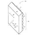
図1は、本発明の第1の実施例に相応した、光伝導性増大部材100を示している。Detailed Description of the Preferred Embodiment FIG. 1 shows a
部材100は図1では、支持板110から形成されている。この支持板は光学的単軸複屈折性結晶材料から成る。これはこの実施例ではフッ化マグネシウム(MgF2)である。In FIG. 1, the
支持板110の光出射表面上には複数のビーム偏光構造120が配置されている。これらのビーム偏光構造はこの実施例では、円柱レンズ121を次のように配列することによって形成されている。すなわち、この円柱レンズ121の長手軸の方向(図1では「D」によってあらわされている)が相互に平行であり、かつ支持板110の光学的単軸結晶材料の光学結晶軸(「oa」によってあらわされている)に対しても平行であるように配列することによって形成されている。 A plurality of
この部材100の円柱レンズ121は、同じく光学的単軸結晶材料上に製造される。すなわち、この実施例では、フッ化マグネシウム(MgF2)から成る。MgF2が使用される代わりに、他の適切な光学的単軸結晶材料を、支持板110または円柱レンズ121に対して使用することもできる。これは、例えばクリスタル・クォーツ(SiO2)、フッ化ランタン(LaF3)およびサファイア(Al2O3)である。The
クリスタル・クォーツを使用している場合には、光学活性が考慮されなければならない。結晶軸が板または基板面において配向され、この板または基板面に対して垂直に視準されて照明に影響が与えられる場合には影響はない。全ての他のケースでは、左旋性石英および右旋性石英を組み合わせることによって悪影響が生じる恐れがある。 If crystal quartz is used, optical activity must be considered. There is no effect if the crystal axis is oriented in the plate or substrate plane and collimated perpendicular to the plate or substrate plane to affect illumination. In all other cases, the combination of levorotatory quartz and dextrorotatory quartz can cause adverse effects.
支持板110および円柱レンズ121は同じ結晶材料を含んでいても、他の異なる結晶材料を含んでいてもよい。さらに、円柱レンズ121は図1に示されている面に対する凸形状の代わりに、凹形状を有していてよく、さらに択一的に支持板110の光入射表面に配置されてよい。 The
図1に示された部材100は、光学システム、殊にマイクロリソグラフィ投影露光装置の照明デバイス(図1には示されていない)において使用され、部材100に入射する光の光伝播方向は図1において矢印130に基づいて示されている。さらに、矢印131は、光の偏光の優先方向をあらわすのに使用される。すなわち、直線偏光された光の場合には、電界ベクトルEの振動の方向である。この実施例では、偏光の優先方向は結晶軸「oa」に対して平行に延在する。同じように有利な実施形態では、点線で描かれた矢印132によって示されているように、偏光の方向が結晶軸「oa」に対して垂直に配向されてもよい。 The
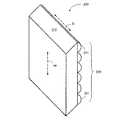
図2に示されている光伝導性増大光学部材200は、図1に示された部材100に相応しており、相応する部材は100足された参照番号で示されている。部材200は、次の点においてのみ部材100と異なる。すなわち支持板210の材料の光学結晶軸「oa」が、円柱レンズ221の長手方向軸の方向(「D」によってあらわされている)に対して垂直に延在しているという点においてのみ部材100と異なる。 The photoconductive enhancement
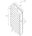
図3では、光学システム300は本発明の別の有利な実施形態に相応して、第1の光伝導性増大部材300a(この実施例においてその構造は、図1に示されたものに相応する)対して付加的に、第2の光伝導性増大部材300bを含む。支持板310の光出射表面に配置された第1の部材300aは、複数の円柱レンズ321を有している。この円柱レンズの長手方向軸(図3において「D1」によってあらわされている)は、図1と同じように、支持板310の結晶材料の光学結晶軸「oa−1」に対して平行である。第1の光伝導性増大部材300aと同じように、第2の光伝導性増大部材300bは、支持板330を含む。この支持板は光学的単軸結晶材料から成る(例えばMgF2)。この材料の結晶軸「oa−2」は、第1の支持板310の結晶材料の光学結晶軸「oa−1」に対して平行である。In FIG. 3, the
第2の部材300bの支持板330の光出射表面に円柱レンズ341の配列340が設けられている。ここでこの円柱レンズ341の長手方向軸の配向(図3において「D2」によってあらわされている)は円柱レンズ321の配向「D1」に対して垂直である。従って、光学システム300は殊に、円柱レンズ321および341の相互に交差した配列320および340を含む。これによってそれぞれ、同じように図3に示されているように、光伝導性が2つの相互に垂直な空間方向において(図面に示された座標軸のx方向およびy方向において)増大される。 An
しかし配列320の円柱レンズ321とは対称的に、配列340の円柱レンズ341は光学的単軸結晶材料を含んでおらず、むしろ光学的等方性材料、殊に立方体結晶材料(cubically crystalline material)から成る。この実施例では、この光学的等方性材料はフッ化カルシウム(CaF2)であるが、動作波長において透過性である他の材料を使用することもできる。これは例えばフッ化ストロンチウム(SrF2)または酸化マグネシウム(MgO)またはYAGである。さらに、択一的な実施形態では、アモルファス材料、殊に石英ガラスも光学的等方性材料として使用可能である。However, in contrast to the
当然ながら、円柱レンズ321および341の配列320および340をそれぞれ択一的に、各支持板310および330の光入射表面に設けてもよい。 Of course, the
図4に示されたさらなる実施形態では、円柱レンズ421と431を有している交差した円柱レンズ配列420と430が、それぞれ、共通の支持板410上に形成されている。支持板410の材料は同じように光学的単軸結晶材料(例えばMgF2)であり、この実施例において光学結晶軸「oa」は、円柱レンズ421の長手方向軸の配向「D1」に対して平行であり、円柱レンズ431の長手方向軸の配向「D2」に対して垂直である。図3と同じように、第1の配列420の円柱レンズ421は、光学的単軸の結晶材料から製造される。ここで第2の配列430を形成している円柱レンズ431は光学的等方性材料から製造される。In a further embodiment shown in FIG. 4, crossed
図5では、本発明に相応する光学システム500の別の実施例において、第1の光伝導性増大部材500aが、インテグレータロッド520の光入射表面に配置されており、第2の光伝導性増大部材500bがインテグレータロッド520の光出射表面に配置されている。第1の光伝導性増大部材と第2の光伝導性増大部材の構造は、それぞれ、図3に示された第1の光伝導性増大部材300aと第2の光伝導性増大部材300bの構造に相当する。従ってここでは詳細に説明しない。 In FIG. 5, in another embodiment of the
インテグレータロッド520は光学的単軸結晶材料から製造されている。これは例えばMgF2である。
図5に相応した配列では、第1の光伝導性増大部材500aは、第1の空間方向において光伝導性における増大をもたらす。すなわち、示された座標系における正および負のy方向において増大をもたらす。インテグレータロッド520を用いて、光混合に同じようにy方向において影響が与えられる。従って、インテグレータロッド520の2つのラテラル表面(図5における上方表面と下方表面)のみが光学的に面平行になるように機械加工されればよい。第2の光伝導性増大部材500bは、第1の空間方向に対して垂直である第2の空間方向(図5では正および負のx方向)において、光伝導性における増大およびインテグレータロッド520から生じる光の混合を生じさせる。 In the arrangement corresponding to FIG. 5, the first
(図示されていない)さらなる実施形態では、別の光伝導性増大部材が図5に示された光伝導性増大部材500bの下流に配置される。このさらなる光伝導性増大部材は、第2の部材500bから生じる光をさらに混合させる。 In a further embodiment (not shown), another photoconductive enhancement member is placed downstream of the
図6では、本発明に相応する光学システム600のさらなる実施例において、第1の光伝導性増大部材610が第1のインテグレータロッド620の光入射表面に配置されており、第2の光伝導性増大部材630がインテグレータロッド620の光出射表面に配置されている。第1の光伝導性増大部材610は、図平面に対して垂直に(図に示された座標系では正および負のx方向において)延在しており、第2の光伝導性増大部材630は図平面において(すなわち、正および負のy方向において)アパーチャ生成(aperture generation)になる。第3の光伝導性増大部材640、第2のインテグレータロッド650、第4の光伝導性増大部材670および第3のインテグレータロッド660は連続して、光伝播方向(x方向)において、第2の光伝導性増大部材630の下流に配置されている。図6の配列の普遍化において、第2の光伝導性増大部材620の下流に配置された光混合デバイスは複数のインテグレータロッド650、660・・・を含んでいる。これらのインテグレータロッドは、光伝播方向に連続して配置されており、これらのインテグレータロッドの間には、さらなる光伝導性増大部材670・・・が各ケースにおいて配置されている。図6の配列では、インテグレータロッド620は同じように有利には、光学的単軸結晶材料(例えばMgF2)から製造されており、光学結晶軸「oa」は、図5の実施例と同じように、第1の光伝導性増大部材610のビーム偏光構造の優先方向に対して平行であり、第2の光伝導性増大部材630のビーム偏光構造の優先方向に対して垂直である(またはその逆)。しかし、上述した実施例とは異なり、光伝導性増大部材610、630、640および670は図6では、回折性光学部材(DOEs)として形成されている。したがって、ビーム回折構造の各優先方向はそれぞれのケースにおいて、前記DOE上の線形構造の延在方向に相当する。In FIG. 6, in a further embodiment of the
インテグレータロッド620とは異なり、インテグレータロッド650および660は光学的等方性材料から形成されている。これはこの実施例ではMgAl2O4である。択一的に、次のことも可能である。すなわち、別の立方体結晶材料または他のアモルファス材料(例えば石英ガラス)を光学的等方性材料として使用することも可能である。Unlike
図6に示されている光学システム600は有利には、マイクロリソグラフィ投影装置の照明デバイスにおいてREMA対物レンズの入力側の上流に配置されている。 The
円柱レンズ配列は光伝導性増大部材として設けられている上述した実施例において、択一的なDOEが配列されてもよい。またその逆もある。 In the above-described embodiment in which the cylindrical lens arrangement is provided as a photoconductive increasing member, an alternative DOE may be arranged. The reverse is also true.
図7と相応に、例えば図3に示された実施例と同じように、第1の支持部711上に配列された第1のDOE712と第2の支持部713上に配列された第2のDOE714を含む、相応する配列710を設けることが可能である。第2のDOEは光伝播方向において下流に配置されており、DOE712および714は各ケースにおいて相互に垂直な空間方向において光伝導性を増大させる。 Corresponding to FIG. 7, for example, as in the embodiment shown in FIG. 3, the
DOEは、公知のように、支持部上に光不透過構造体を形成することによって形成されるか、または屈折率の変化および/または幾何学的形状の厚さの変化を伴い、光透過性構造体を特定の領域に形成することによって形成される。DOEのこのような構造化は例えば、光学的単軸結晶材料から成る支持体板において相応する材料を除去することによって行われる。さらなる実施例では、石英ガラスから成るアモルファス層が、光学的単軸結晶材料から成る支持板上に蒸着されてもよい。この層内ではエッチングによってパターニングが連続的に導入される。後者の実施例は次のような利点を有している。すなわち、結晶支持板を直接的にパターニングする場合よりも、アモルファス層をパターンニングする場合においては、構造体内のエッジのより多い統一形状が可能であるという利点を有している。 The DOE is formed by forming a light-impermeable structure on the support, as known in the art, or is accompanied by a change in refractive index and / or a change in the thickness of the geometric shape. It is formed by forming a structure in a specific region. Such structuring of the DOE is performed, for example, by removing the corresponding material in a support plate made of optical uniaxial crystal material. In a further embodiment, an amorphous layer made of quartz glass may be deposited on a support plate made of an optical uniaxial crystal material. Within this layer, patterning is continuously introduced by etching. The latter embodiment has the following advantages. That is, the patterning of the amorphous layer has the advantage that a unified shape with more edges in the structure is possible than when the crystal support plate is directly patterned.
図7aの配列710では、支持部711(ひいてはDOEが組み込まれている形状の場合には、DOE712の構造)は、光学的単軸結晶材料(例えばMgF2)から製造される。第2の光伝導性増大部材が組み込まれている形状の場合(支持部713において材料を除去することによってDOE714を形成することによって)には、有利には支持部713は、図3の実施例と同じように光学的等方性材料から製造される。すなわち、立方体結晶性材料またはアモルファス材料(例えば石英ガラス)から製造される。しかし1つの有利な実施形態では、第2の支持部713は、第1の支持部と同じように光学的単軸結晶材料から製造され、DOE714は蒸着および、殊に石英ガラスから成るアモルファス層の連続するエッチングによって製造される。In the
当然ながらDOE712、714が、支持部711および713の各光入射表面上に配置されてもよい。 Of course, the
さらに図7bに相応して、DOE722および723を共通の支持部721上に配置することも可能である。この配列720では、支持部721は光学的単軸結晶材料(例えばMgF2)から製造され、支持部721の光出射表面に配置されたDOE723は上述のように、蒸着および例えば石英ガラスから成るアモルファス層をエッチングすることによって形成される。支持部721の光入射表面に配列されたDOE722が随意に光学的単軸結晶材料から形成され(すなわち殊に相応する材料を除去することによって支持板721と一体化し)てもよく、または同じように、蒸着および例えば石英ガラスから成るアモルファス層をエッチングすることによって形成されてもよい。Furthermore, DOEs 722 and 723 can be arranged on a
さらに、図7cに示されているように、より複雑なDOE構造732を、支持部731(同じように光学的単軸結晶材料から成る)上の任意の空間方向における偏光によって形成することが可能である。この構造は同じように、蒸着および例えば石英ガラスから成るアモルファス層のエッチングによって形成される。 Furthermore, as shown in FIG. 7c, a more
別の有利な実施形態では、上述したように光学的単軸結晶材料を有している本発明に相応して使用されている回折性光学部材(DOE)に、所望のように放射強度を所望の次の回折(殊に、例えば1次の回折)に向けるために、ブレーズ効果が付与される。このために、それ自体公知の方法で、各DOEは典型的に、図8aの概略的に例示された配列800において示されているように、相応する周期的な構造体801、802、803・・・等を伴う鋸歯状プロファイルまたは階段状プロファイルとともに形成される。 In another advantageous embodiment, a diffractive optical element (DOE) used in accordance with the present invention having an optically uniaxial crystal material as described above has a desired radiation intensity as desired. A blaze effect is imparted to the next diffraction (especially, for example, the first diffraction). For this purpose, in a manner known per se, each DOE is typically associated with a corresponding
別の有利な実施形態では、本発明に相応するDOEは光学的単軸結晶材料を有し、上述のように偏光選択形式で次のように形成されている。すなわち、相互に直交している2つの偏光状態(殊にs偏光とp偏光)のうちの1つの偏光状態に対して、他方の偏光状態に対するよりも高いブレーズ効果が生じるように形成されている。例えばDOEは次のように形成されている。すなわち、DOEに入射する光のs偏光された成分が主に±1次の回折に向けられ、DOEに入射する光のp偏光された成分が主に0次の回折に向けられるように形成される。 In another advantageous embodiment, a DOE according to the invention comprises an optical uniaxial crystal material and is formed in the polarization selective manner as described above as follows. That is, it is formed such that a higher blazing effect is produced for one of the two polarization states (especially s-polarization and p-polarization) orthogonal to each other than for the other polarization state. . For example, the DOE is formed as follows. That is, the s-polarized component of light incident on the DOE is mainly directed to ± 1st-order diffraction, and the p-polarized component of light incident on the DOE is mainly directed to 0th-order diffraction. The
図8bでは、回折性光学部材は第1のブレーズ格子810と、この第1のブレーズ格子810の光出射面に重畳された第2のブレーズ格子820を有している。この場合には、第2のブレーズ格子820は構造体820a〜820eの配列を有している。これらの構造体は、櫛の歯形状またはリブ付けされたものとして示されている。個々の構造体820a〜820e(これらは概略的に示されているだけであり、典型的に、より多数である)は、DOEが設計されている(例えばλ=193nmの)動作波長よりも小さい。 In FIG. 8 b, the diffractive optical member has a first blazed grating 810 and a second blazed grating 820 superimposed on the light exit surface of the first blazed grating 810. In this case, the second blazed grating 820 has an array of
図8bの実施例では、サブ構造体820a〜820eのサブ波長構造を有するブレーズ格子820において、充填比は、左から右へブレーズ格子820の延在方向「D」に沿って低減している。この場合には「充填比」とは、サブ波長構造を有するブレーズ格子820の周期「g」に相対する、延在方向「D」におけるサブ構造体820a〜820eの寸法の比である。従って第1の回折格子810の各周期内でのサブ構造体820a〜820eの幅は、延在方向「D」において、左から右へ、所与の相応する最適化において低減する。これは次のような効果を得るためである。すなわち、DOEに入射する光のs偏光された成分が主に1次回折に向けられ、DOEに入射する光のp偏光された成分が主に0次回折に向けられるという効果を得るためである。 In the example of FIG. 8b, in the blazed grating 820 having the sub-wavelength structure of the
相互に直交する2つの偏光状態のうちの1つの偏光状態に対してのみブレーズ効果を最適化するために、偏光選択作用と組み合わされたブレーズ効果を伴ってDOEを形成することは、概略的に図8bで示された配列850に限定されるものではない。従ってサブ構造体820a〜820eを統一して(すなわち、一定の幅および長さで)、第2のブレーズ格子820の周期にわたって、それ自体公知の方法で、所望の所与の相応する最適化において形成することも可能である。これによって、例えば(±1次)の回折に向かったs偏光された成分の偏光が得られる。さらに、図8bに示された配列の変形において、サブ構造体820a〜820eを一定の幅と可変の長さ(すなわち、ブレーズ格子820の延在方向「D」に対して垂直に可変に延在する)を以て形成することもできる。例えば、左から右へ、延在方向「D」において第1の回折格子810の各周期内で低減する長さで以て形成することもできる。 Forming a DOE with a blaze effect combined with a polarization selective action in order to optimize the blaze effect only for one of the two polarization states orthogonal to each other is schematically It is not limited to the
本発明に相応するDOEの別の可能な実施形態の構造は概略的に図8c〜eに示されている。 The structure of another possible embodiment of a DOE corresponding to the present invention is shown schematically in FIGS.
図8cに相応して、例えば、DOEの部分領域860に基づいて示されているように、典型的なDOE構造体861、862および863は、例えばクォーツまたはサファイア(Al2O3)から成る結晶基板材料における相応する材料除去によって形成される。図8dは、さらなるDOEの部分領域870に基づいて、DOE構造体872、873および874を示している。これらの構造体は、クリスタル・クォーツまたはサファイア(Al2O3)から成る基板871上に被着されており、複数の層から成る多層構造を含む。ここでこれらの層はそれぞれ、酸化物化合物またはフッ化物化合物(例えばMgF2またはAl2O3)を含む。図8eは、DOEの部分領域880に基づいて、一体化されたDOE構造体882、883および884を示している。これらの構造体は、例えばクリスタル・クォーツまたはサファイア(Al2O3)から成る基板881上に被着されており、各ケースにおいて、酸化物化合物またはフッ化物化合物、例えばフッ化カルシウム(CaF2)を含む。Corresponding to FIG. 8c,
それぞれ使用されている光学的単軸結晶材料の光学結晶軸は、殊に基板(すなわち例えばクリスタル・クォーツ)において、基板表面に対して平行である。有利には、それぞれ基板において使用されている光学的単軸結晶材料の光学結晶軸は、さらに、ビーム偏光構造体の優先方向に対して平行であるかまたは垂直であり、さらに、光伝導性増大部材に入射する光の偏光の優先方向に対して平行であるか、または垂直である。さらに、基板は有利には、使用されている動作波長(例えば193nmまたは157nm)の整数倍の厚さを有している。 The optical crystal axis of each optical uniaxial crystal material used is parallel to the substrate surface, especially in the substrate (ie crystal quartz, for example). Advantageously, the optical crystal axis of each optical uniaxial crystal material used in the substrate is further parallel or perpendicular to the preferred direction of the beam polarization structure, and further increases the photoconductivity. It is parallel or perpendicular to the preferred direction of polarization of light incident on the member. Furthermore, the substrate advantageously has a thickness that is an integral multiple of the operating wavelength used (eg 193 nm or 157 nm).
図9は、計算機ホログラム(CGH)900として実現されている、本発明に相応する光伝導性増大部材を説明するための概略図を示している。CGH900は、自身の光出射面901上にファセット領域のアレイを含む(図示されていない)。これらのファセット領域はそれぞれ構造体を含む。この構造体は、計算機によって計算され、それぞれ所望のビーム回折作用が得られるまたは角度展開が得られる。 FIG. 9 shows a schematic diagram for explaining a photoconductive enhancement member corresponding to the present invention, which is realized as a computer generated hologram (CGH) 900.
CGH900は、入射光910aに対して所望の二次元強度分布を形成する。この二次元強度分布は図9に相応して四重極分布920である。これは、各ビーム回折構造によって定められた角度放射特性による。 The
計算機ホログラム(CGH)は基板902も含む。この基板は複屈折性の、光学単軸材料から成る。これは例えばクリスタル・クォーツ(SiO2)、フッ化マグネシウム(MgF2)、フッ化ランタン(LaF3)またはサファイア(Al2O3)である。CGH900として実現される場合には、光伝導性増大部材の優先方向に関して言えば、この優先方向はここで照明デバイスの光軸(これは図9では、CGH900の中心を通って、z方向に沿って延在する)から、二次元強度分布の極に向かって(すなわち、図9の例においては四重極分布920の中心から四重極分布920の4つの極の1つへ)配向されている方向として定められる。すなわち四重極分布920によって定められた正方形内の対角線に沿っている。The computer generated hologram (CGH) also includes a
基板902の結晶材料の光学結晶軸は実質的にこの優先方向に平行であるか、または実質的に垂直である。基板902の光学単軸材料における光学結晶軸oaの可能な配向は、図9において斜めの矢印によって示されている。別の可能な配向は、xーy面における図示された配向に対して垂直である。 The optical crystal axis of the crystal material of the
ある実施形態では、ファセット領域のアレイは次のように形成される。すなわち、前記計算機ホログラム(CGH)の構造が、隣接するファセット領域との間の境界にわたって不連続性を有していないように形成される。換言すれば、計算機ホログラム(CGH)の個々のファセット領域内に設けられた構造は、隣接するファセット領域間の領域にわたって実質的に連続的に機能する。隣接するファセット領域間の不連続性(例えばエッジ、破断部等)を回避することによって、隣接するファセット領域の間の境界で、位相機能の連続する移行が得られる。これによって、このような境界で強度変化が生じることが阻止される。 In one embodiment, the array of facet regions is formed as follows. That is, the structure of the computer generated hologram (CGH) is formed so as not to have discontinuities across the boundary between the adjacent facet regions. In other words, structures provided within individual facet regions of a computer generated hologram (CGH) function substantially continuously across the region between adjacent facet regions. By avoiding discontinuities (eg, edges, breaks, etc.) between adjacent facet regions, a continuous transition of phase function is obtained at the boundary between adjacent facet regions. This prevents intensity changes from occurring at such boundaries.
別の実施形態では、ファセット領域のアレイは次のように形成される。すなわち、この計算機ホログラムの構造が、隣接するファセット領域の間の境界にわたって不連続性を含むように形成される。これはより大きい設計の自由性を得るのに有利である。 In another embodiment, the array of faceted regions is formed as follows. That is, the computer generated hologram structure is formed to include discontinuities across the boundaries between adjacent facet regions. This is advantageous for greater design freedom.
さらに、ファセット領域のアレイは次のように形成される。すなわち、計算機ホログラム(CGH)の構造がファセット領域のうちの1つのファセット領域において模写されるように形成される。これは、異なるファセット領域に属する構造の相互作用によって繰り返される不所望な強度変化を回避するのに有利である。択一的にファセット領域のアレイは次のように形成される。すなわち、計算機ホログラム(CGH)の構造がこのファセット領域の少なくとも1つのファセット領域において模写されるように形成される。 Further, the array of facet regions is formed as follows. That is, the structure of the computer generated hologram (CGH) is formed so as to be replicated in one facet region of the facet regions. This is advantageous in avoiding undesired intensity changes due to the interaction of structures belonging to different facet regions. Alternatively, the array of facet regions is formed as follows. That is, the structure of the computer generated hologram (CGH) is formed so as to be replicated in at least one facet region of the facet region.
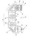
図10は概略図において、マイクロリソグラフィ投影露光装置133を示している。これは光源ユニット135と、照明デバイス139と、構造搬送マスク153と、投影対物レンズ155と露光される基板159を含む。光源ユニット135は光源として、例えば、193nmの動作波長に対するArFレーザを含み、平行光束を形成するビーム形成光学系も含む。 FIG. 10 schematically shows a microlithographic
この実施例では、平行光束は最初に光伝導性増大部材137に入射する。ここでこの光伝導性増大部材は、所望の強度分布を形成する。これは例えば二重極分布または四重極分布である。これは、瞳面145内の個々の回折性または屈折性のビーム回折構造を用いて行われる。この光伝導性増大部材は、上述の実施形態において記述されたように構成されている。ズーム対物レンズ140は、光伝播方向において光伝導性増大部材137の下流に配置され、可変の直径を有する平行光束を形成する。平行光束は偏光ミラー141によって光学ユニット142に向けられ、この光学ユニットはアキシコン143を有する。上流の光伝導性増大部材137およびアキシコン143と関連するズーム対物レンズ140によって、ズームセッティングおよびアキシコン部材の位置に依存して、瞳面145において異なった照明構造が形成される。光学ユニット142はアキシコン143の下流で、瞳面145の領域内に配置されている光混合システム148を含む。この光混合システムはこのケースではそれ自体公知の様式で、光混合を得るのに適したマイクロ光学部材(図10において部材146および147によってあらわされている)の配列を有している。 In this embodiment, the parallel light beam first enters the
光混合システム148は択一的に、フライズアイコンデンサまたはロッドインテグレータであってよい。これは、動作波長を有する光を透過する材料から成る。これは例えば石英ガラスまたは他の結晶性フッ化カルシウムである。光学ユニット142にはレチクルマスキングシステム(REMA)149が続く。これは、REMA対物レンズ151によって構造搬送マスク(レチクル)153上に結像され、これによってレチクル153上の照明された領域に境界が定められる。構造搬送マスク153は、投影対物レンズ155によって感光基板159上に結像される。図示された実施例では、空気とは異なる屈折率を有する液浸液161が、投影対物レンズ155の最後の光学部材157と感光基板159の間に配置されている。 The
本発明を、特定の実施例に基づいて説明したが、当業者によって、例えば各実施形態の特徴を組み合わせるおよび/または交換することによって、種々の変更および択一的な実施例を導出することができる。従ってこのような変更および択一的な実施形態も本発明に含まれることは当業者にとって自明のことであり、本発明の範囲は添付された特許請求範囲およびそれに相当するものによってのみ制限される。 Although the present invention has been described with reference to specific examples, various modifications and alternative examples can be derived by those skilled in the art, for example, by combining and / or exchanging features of each embodiment. it can. Accordingly, it will be apparent to those skilled in the art that such modifications and alternative embodiments are also encompassed by the present invention, and the scope of the present invention is limited only by the appended claims and equivalents thereof. .
100、200、300a、400、500a、610、900 第1の光伝導性増大部材、 D1 第1の優先方向、 110、210、310、330 支持板、 120 ビーム偏光構造体、 121、221、321、421、431、511 円柱レンズ、 300b、500b、630 第2の光伝導性増大部材、 320、340、410、420、430 円柱レンズ配列、 500、600 光学システム、 520、620、650、660 インテグレータロッド、 640 第3の光伝導性増大部材、 670 第4の光伝導性増大部材、 710、720、730、800 配列、 711、721、731 支持部、 712、714、722、723 DOE、 801、802、803 構造体、 810 第1のブレーズ格子、 820 第2のブレーズ格子、 820a〜820e サブ構造体、 860、870、880 DOE、 861、862、863、872、873、874、882、883、884 DOEの部分領域、 871、881 基板、 901 光出射面、 902 基板、 920 四重極分布、 133 マイクロリソグラフィ投影露光装置、 135 光源ユニット、 139 照明デバイス、 153 構造搬送マスク、 155 投影対物レンズ、 159 基板、 137 光伝導性増大部材、 145 瞳面、 140 ズーム対物レンズ、 141 偏光ミラー、 142 光学ユニット、 143 アキシコン、 146、147 マイクロ光学部材、 148 光混合システム、 149 レチクルマスキングシステム(REMA)、 151 REMA対物レンズ、 153 構造搬送マスク(レチクル)、 155 投影対物レンズ、 159 感光基板、 161 液浸液、 157 投影対物レンズの最後の光学部材 100, 200, 300a, 400, 500a, 610, 900 First photoconductive enhancement member, D1 First preferred direction, 110, 210, 310, 330 Support plate, 120 Beam polarization structure, 121, 221 and 321 , 421, 431, 511 cylindrical lens, 300b, 500b, 630 second photoconductive enhancement member, 320, 340, 410, 420, 430 cylindrical lens array, 500, 600 optical system, 520, 620, 650, 660 integrator Rod, 640 Third photoconductive enhancement member, 670 Fourth photoconductive enhancement member, 710, 720, 730, 800 Array, 711, 721, 731 Support, 712, 714, 722, 723 DOE, 801, 802, 803 structure, 810 first blaze grating 820 second blazed grating, 820a-820e sub-structure, 860, 870, 880 DOE, 861, 862, 863, 872, 873, 874, 882, 883, 884 DOE, 871, 881 substrate, 901 light Emitting surface, 902 substrate, 920 quadrupole distribution, 133 microlithography projection exposure apparatus, 135 light source unit, 139 illumination device, 153 structure transfer mask, 155 projection objective lens, 159 substrate, 137 photoconductivity increasing member, 145 pupil plane , 140 zoom objective lens, 141 polarizing mirror, 142 optical unit, 143 axicon, 146, 147 micro optical member, 148 light mixing system, 149 reticle masking system (REMA), 151 RE MA objective lens, 153 structure transfer mask (reticle), 155 projection objective lens, 159 photosensitive substrate, 161 immersion liquid, 157 last optical member of projection objective lens
Claims (44)
Translated fromJapanese・少なくとも1つの第1の光伝導性増大部材(100、200、300a、400、500a、900)を含み、当該第1の光伝導性増大部材は複数の回折性または屈折性ビーム偏光構造体を有しており、当該構造体は共通の第1の優先方向(D1)に延在しており;
・前記光伝導性増大部材は光学的単軸結晶材料を有しており、当該結晶材料の光学結晶軸は、前記第1の優先方向(D1)に対して実質的に平行であるか、または実質的に垂直である、
ことを特徴とする、マイクロリソグラフィ投影露光装置の照明デバイスの光学システム。An optical system of an illumination device of a microlithographic projection exposure apparatus, the optical system comprising:
At least one first photoconductive enhancement member (100, 200, 300a, 400, 500a, 900), wherein the first photoconductive enhancement member comprises a plurality of diffractive or refractive beam polarizing structures; And the structure extends in a common first preferred direction (D1);
The photoconductive enhancement member comprises an optical uniaxial crystal material, the optical crystal axis of the crystal material being substantially parallel to the first preferred direction (D1), or Is substantially vertical,
An optical system for an illumination device of a microlithographic projection exposure apparatus.
当該結晶材料の光学結晶軸は前記基板の表面に対して実質的に平行に配向されている、請求項1または2記載の光学システム。The beam polarization structure is formed on a substrate, and the substrate is made of an optical uniaxial crystal material;
The optical system according to claim 1 or 2, wherein the optical crystal axis of the crystal material is oriented substantially parallel to the surface of the substrate.
当該ブレーズ格子のうちの少なくとも1つの格子構造は、回折性光学部材(DOE)が設計されている動作波長よりも小さい、請求項16または17記載の光学システム。The diffractive optical member (DOE) has a first blazed grating (810) and at least one second blazed grating (820);
18. An optical system according to claim 16 or 17, wherein at least one of the blazed gratings has a grating structure that is smaller than the operating wavelength for which the diffractive optical element (DOE) is designed.
複数の回折性または屈折性のビーム偏光構造を有しており、
当該ビーム偏光構造は第2の優先方向に延在しており、当該第2の優先方向は第1の優先方向とは異なっている、請求項1から27までのいずれか1項記載の光学システム。The second photoconductive increase member (300b, 500b) is disposed downstream of the first photoconductive increase member (300a, 500a) in the light propagation direction,
Having a plurality of diffractive or refractive beam polarization structures;
28. The optical system according to any one of claims 1 to 27, wherein the beam polarization structure extends in a second preferred direction, and the second preferred direction is different from the first preferred direction. .
当該基板は、使用されている動作波長の整数倍の厚さを有している、請求項1から36までのいずれか1項記載の光学システム。At least one photoconductive enhancement member has a substrate made of an optically uniaxial crystal material;
37. An optical system according to any one of claims 1-36, wherein the substrate has a thickness that is an integral multiple of the operating wavelength being used.
当該回折性光学部材は少なくとも1つの第1のブレーズ格子(810)と第2のブレーズ格子(820)を含み、
当該第2のブレーズ格子(820)は前記第1のブレーズ格子(810)の光出射表面上に重畳しており、実質的にリブが付けられたサブ構造体(820a、820e)の配列を有しており、
当該サブ構造体は、回折性光学部材(DOE)が設計されている動作波長よりも小さい形式のものにおいて、
前記回折性光学部材は光学的単軸結晶材料を有しており、当該結晶材料の光学結晶軸は、第1および/または第2のブレーズ格子の格子構造に対して実質的に平行であるか、または実質的に垂直である、
ことを特徴とする回折性光学部材。A diffractive optical member,
The diffractive optical member includes at least one first blazed grating (810) and a second blazed grating (820);
The second blazed grating (820) is superimposed on the light emitting surface of the first blazed grating (810), and has a substantially ribbed substructure (820a, 820e) arrangement. And
The substructure is of a type smaller than the operating wavelength for which the diffractive optical member (DOE) is designed,
The diffractive optical member has an optical uniaxial crystal material, and is the optical crystal axis of the crystal material substantially parallel to the lattice structure of the first and / or second blazed grating? Or is substantially vertical,
A diffractive optical member characterized by the above.
当該回折性光学部材は少なくとも1つの第1のブレーズ格子(810)と第2のブレーズ格子(820)を含み、
当該第2のブレーズ格子(820)は前記第1のブレーズ格子(810)の光出射表面上に重畳しており、実質的にリブが付けられたサブ構造体(820a〜820e)の配列を有しており、
当該サブ構造体は、回折性光学部材(DOE)が設計されている動作波長よりも小さい形式において、
前記回折性光学部材は光学的単軸結晶材料を有しており、当該結晶材料はフッ化マグネシウム(MgF2)、フッ化ランタン(LaF3)およびサファイア(Al2O3)を含むグループから選択される、
ことを特徴とする回折性光学部材。A diffractive optical member,
The diffractive optical member includes at least one first blazed grating (810) and a second blazed grating (820);
The second blazed grating (820) is superimposed on the light emitting surface of the first blazed grating (810), and has a substantially ribbed substructure (820a to 820e) arrangement. And
The substructure is in a form smaller than the operating wavelength for which the diffractive optical member (DOE) is designed,
The diffractive optical member has an optical uniaxial crystal material, and the crystal material is selected from the group including magnesium fluoride (MgF2 ), lanthanum fluoride (LaF3 ), and sapphire (Al2 O3 ). To be
A diffractive optical member characterized by the above.
当該回折性光学部材は少なくとも1つの第1のブレーズ格子(810)と第2のブレーズ格子(820)を含み、
当該第2のブレーズ格子(820)は前記第1のブレーズ格子(810)の光出射表面上に重畳しており、実質的にリブが付けられたサブ構造体(820a〜820e)の配列を有しており、
当該サブ構造体は、回折性光学部材(DOE)が設計されている動作波長よりも小さい形式において、
前記回折性光学部材は、元来複屈折の、非光学活性結晶材料を有している、
ことを特徴とする回折性光学部材。A diffractive optical member,
The diffractive optical member includes at least one first blazed grating (810) and a second blazed grating (820);
The second blazed grating (820) is superimposed on the light emitting surface of the first blazed grating (810), and has a substantially ribbed substructure (820a to 820e) arrangement. And
The substructure is in a form smaller than the operating wavelength for which the diffractive optical member (DOE) is designed,
The diffractive optical member originally has a birefringent, non-optically active crystalline material,
A diffractive optical member characterized by the above.
請求項1から36のいずれか1項に記載された光学システムおよび/または請求項37から40のいずれか1項記載の回折性光学部材を有している、
ことを特徴とする、マイクロリソグラフィ投影露光装置の照明デバイス。An illumination device of a microlithographic projection exposure apparatus,
The optical system according to any one of claims 1 to 36 and / or the diffractive optical member according to any one of claims 37 to 40,
An illumination device for a microlithographic projection exposure apparatus, characterized in that:
・感光性材料から成る層が少なくとも部分的に加えられている基板(159)を設けるステップと;
・結像される構造を有するマスク(153)を設けるステップと;
・請求項42記載の投影露光装置(133)を設けるステップと;
・前記投影露光装置(133)を用いて、前記層の領域上に前記マスク(153)の少なくとも一部分を投影するステップとを有する、マイクロ構造化コンポーネントのマイクロリソグラフィ製造のための方法。A method for the microlithographic manufacture of a microstructured component, the method comprising the following steps:
Providing a substrate (159) to which a layer of photosensitive material has been at least partially applied;
Providing a mask (153) having a structure to be imaged;
Providing a projection exposure apparatus (133) according to claim 42;
Projecting at least a portion of the mask (153) onto an area of the layer using the projection exposure apparatus (133).
Applications Claiming Priority (4)
| Application Number | Priority Date | Filing Date | Title |
|---|---|---|---|
| US78208906P | 2006-03-14 | 2006-03-14 | |
| US60/782089 | 2006-03-14 | ||
| DE102006012034ADE102006012034A1 (en) | 2006-03-14 | 2006-03-14 | Optical system e.g. lighting device, for use in microlithographic projection lighting system, has light-conductance-increasing unit with set of diffractive or refractive beam deflecting structures extending in common direction |
| DE102006012034.5 | 2006-03-14 |
Publications (3)
| Publication Number | Publication Date |
|---|---|
| JP2007258709Atrue JP2007258709A (en) | 2007-10-04 |
| JP2007258709A5 JP2007258709A5 (en) | 2010-04-30 |
| JP5179077B2 JP5179077B2 (en) | 2013-04-10 |
Family
ID=38374829
Family Applications (1)
| Application Number | Title | Priority Date | Filing Date |
|---|---|---|---|
| JP2007064831AActiveJP5179077B2 (en) | 2006-03-14 | 2007-03-14 | Optical system for illumination device of projection exposure apparatus |
Country Status (4)
| Country | Link |
|---|---|
| US (1) | US8068279B2 (en) |
| EP (1) | EP1835312B1 (en) |
| JP (1) | JP5179077B2 (en) |
| DE (2) | DE102006012034A1 (en) |
Cited By (4)
| Publication number | Priority date | Publication date | Assignee | Title |
|---|---|---|---|---|
| JP2009302155A (en)* | 2008-06-10 | 2009-12-24 | Canon Inc | Computer-generated hologram, exposure apparatus and device method for manufacturing |
| JP2009302156A (en)* | 2008-06-10 | 2009-12-24 | Canon Inc | Computer-generated hologram, exposure apparatus and device method for manufacturing method |
| JP2011133640A (en)* | 2009-12-24 | 2011-07-07 | Dainippon Printing Co Ltd | Method for producing transmissive hologram |
| WO2020153504A1 (en)* | 2019-01-25 | 2020-07-30 | 大日本印刷株式会社 | Diffractive optical device, illumination apparatus, projection apparatus, projection display apparatus, and method for manufacturing element diffractive optical device |
Families Citing this family (16)
| Publication number | Priority date | Publication date | Assignee | Title |
|---|---|---|---|---|
| TWI545352B (en)* | 2006-02-17 | 2016-08-11 | 卡爾蔡司Smt有限公司 | Illumination system for a microlithographic projection exposure apparatus |
| KR101254843B1 (en)* | 2006-02-17 | 2013-04-15 | 칼 짜이스 에스엠티 게엠베하 | Optical integrator for an illumination system of a microlithographic projection exposure apparatus |
| DE102009016608A1 (en) | 2008-05-21 | 2009-11-26 | Carl Zeiss Smt Ag | Illumination optic for a microlithography projection exposure system for illuminating an object field with illumination light of a radiation source, comprises an optical beam forming element, and a group of beam formation sections |
| CN103097925B (en)* | 2010-08-06 | 2016-04-13 | 旭硝子株式会社 | Diffraction optical element and measuring device |
| US8902485B2 (en) | 2012-11-29 | 2014-12-02 | Christie Digital Systems Usa, Inc. | Contrast enhancing system |
| EP2754524B1 (en) | 2013-01-15 | 2015-11-25 | Corning Laser Technologies GmbH | Method of and apparatus for laser based processing of flat substrates being wafer or glass element using a laser beam line |
| EP2781296B1 (en) | 2013-03-21 | 2020-10-21 | Corning Laser Technologies GmbH | Device and method for cutting out contours from flat substrates using a laser |
| US11556039B2 (en) | 2013-12-17 | 2023-01-17 | Corning Incorporated | Electrochromic coated glass articles and methods for laser processing the same |
| US10293436B2 (en) | 2013-12-17 | 2019-05-21 | Corning Incorporated | Method for rapid laser drilling of holes in glass and products made therefrom |
| CN106687419A (en) | 2014-07-08 | 2017-05-17 | 康宁股份有限公司 | Methods and apparatuses for laser processing materials |
| KR20170028943A (en)* | 2014-07-14 | 2017-03-14 | 코닝 인코포레이티드 | System for and method of processing transparent materials using laser beam focal lines adjustable in length and diameter |
| HUE055461T2 (en) | 2015-03-24 | 2021-11-29 | Corning Inc | Laser cutting and processing of display glass compositions |
| US10730783B2 (en) | 2016-09-30 | 2020-08-04 | Corning Incorporated | Apparatuses and methods for laser processing transparent workpieces using non-axisymmetric beam spots |
| EP3529214B1 (en) | 2016-10-24 | 2020-12-23 | Corning Incorporated | Substrate processing station for laser-based machining of sheet-like glass substrates |
| CN106647179A (en)* | 2016-11-25 | 2017-05-10 | 天津津芯微电子科技有限公司 | Compound-eye light homogenization system, optical engine and light source optimization device |
| CN114137655B (en)* | 2020-09-04 | 2022-12-23 | 宁波舜宇光电信息有限公司 | Optical waveguide device for AR apparatus, method of manufacturing the same, and AR apparatus |
Citations (6)
| Publication number | Priority date | Publication date | Assignee | Title |
|---|---|---|---|---|
| JP2000206321A (en)* | 1999-01-19 | 2000-07-28 | Canon Inc | Diffractive optical element, optical system having diffractive optical element, method of manufacturing diffractive optical element, exposure apparatus including optical system having diffractive optical element, and method of manufacturing device using exposure apparatus |
| JP2003035822A (en)* | 2001-05-22 | 2003-02-07 | Carl Zeiss Semiconductor Manufacturing Technologies Ag | Polariscope and microlithography projection system provided with the same |
| JP2003090959A (en)* | 2001-09-17 | 2003-03-28 | Ricoh Co Ltd | Laser illumination optical system, exposure apparatus using the optical system, laser processing machine, and projection apparatus |
| JP2005032909A (en)* | 2003-07-10 | 2005-02-03 | Fuji Photo Film Co Ltd | Lighting optical system and aligner using it |
| WO2005026822A2 (en)* | 2003-09-15 | 2005-03-24 | Carl Zeiss Smt Ag | Fly's eye condenser and illumination system therewith |
| JP2005268489A (en)* | 2004-03-18 | 2005-09-29 | Canon Inc | Illumination apparatus, exposure apparatus, and device manufacturing method |
Family Cites Families (9)
| Publication number | Priority date | Publication date | Assignee | Title |
|---|---|---|---|---|
| US5610733A (en)* | 1994-02-28 | 1997-03-11 | Digital Optics Corporation | Beam-homogenizer |
| US5850300A (en)* | 1994-02-28 | 1998-12-15 | Digital Optics Corporation | Diffractive beam homogenizer having free-form fringes |
| JP2001343512A (en)* | 2000-05-31 | 2001-12-14 | Canon Inc | Diffractive optical element and optical system having the same |
| JP4310080B2 (en)* | 2002-06-17 | 2009-08-05 | キヤノン株式会社 | Diffractive optical element and optical system and optical apparatus provided with the same |
| GB2403815A (en)* | 2003-07-10 | 2005-01-12 | Ocuity Ltd | Birefringent lens array structure |
| US20070019179A1 (en)* | 2004-01-16 | 2007-01-25 | Damian Fiolka | Polarization-modulating optical element |
| EP1754111A1 (en)* | 2004-06-10 | 2007-02-21 | Carl Zeiss SMT AG | Lighting unit of a microlithographic projection exposure system |
| DE102005030543A1 (en)* | 2004-07-08 | 2006-02-02 | Carl Zeiss Smt Ag | Polarizer device for illumination system, has interference device converting light beam with angular distribution to another beam, and decoupling device receiving latter beam and emitting beam with another angular distribution |
| DE102005039519A1 (en) | 2005-08-20 | 2007-02-22 | Carl Zeiss Smt Ag | Projection illumination equipment for manufacturing semiconductor component, has cuboid shaped light conducting rod, and crystallographic main axis extending approximately perpendicular or parallel to longitudinal extension of rod |
- 2006
- 2006-03-14DEDE102006012034Apatent/DE102006012034A1/ennot_activeWithdrawn
- 2007
- 2007-03-09DEDE602007014285Tpatent/DE602007014285D1/enactiveActive
- 2007-03-09EPEP07103867Apatent/EP1835312B1/ennot_activeCeased
- 2007-03-13USUS11/685,620patent/US8068279B2/enactiveActive
- 2007-03-14JPJP2007064831Apatent/JP5179077B2/enactiveActive
Patent Citations (7)
| Publication number | Priority date | Publication date | Assignee | Title |
|---|---|---|---|---|
| JP2000206321A (en)* | 1999-01-19 | 2000-07-28 | Canon Inc | Diffractive optical element, optical system having diffractive optical element, method of manufacturing diffractive optical element, exposure apparatus including optical system having diffractive optical element, and method of manufacturing device using exposure apparatus |
| JP2003035822A (en)* | 2001-05-22 | 2003-02-07 | Carl Zeiss Semiconductor Manufacturing Technologies Ag | Polariscope and microlithography projection system provided with the same |
| JP2003090959A (en)* | 2001-09-17 | 2003-03-28 | Ricoh Co Ltd | Laser illumination optical system, exposure apparatus using the optical system, laser processing machine, and projection apparatus |
| JP2005032909A (en)* | 2003-07-10 | 2005-02-03 | Fuji Photo Film Co Ltd | Lighting optical system and aligner using it |
| WO2005026822A2 (en)* | 2003-09-15 | 2005-03-24 | Carl Zeiss Smt Ag | Fly's eye condenser and illumination system therewith |
| JP2007506262A (en)* | 2003-09-15 | 2007-03-15 | カール・ツァイス・エスエムティー・アーゲー | Fly eye condenser and illumination system using the same |
| JP2005268489A (en)* | 2004-03-18 | 2005-09-29 | Canon Inc | Illumination apparatus, exposure apparatus, and device manufacturing method |
Cited By (5)
| Publication number | Priority date | Publication date | Assignee | Title |
|---|---|---|---|---|
| JP2009302155A (en)* | 2008-06-10 | 2009-12-24 | Canon Inc | Computer-generated hologram, exposure apparatus and device method for manufacturing |
| JP2009302156A (en)* | 2008-06-10 | 2009-12-24 | Canon Inc | Computer-generated hologram, exposure apparatus and device method for manufacturing method |
| JP2011133640A (en)* | 2009-12-24 | 2011-07-07 | Dainippon Printing Co Ltd | Method for producing transmissive hologram |
| WO2020153504A1 (en)* | 2019-01-25 | 2020-07-30 | 大日本印刷株式会社 | Diffractive optical device, illumination apparatus, projection apparatus, projection display apparatus, and method for manufacturing element diffractive optical device |
| JPWO2020153504A1 (en)* | 2019-01-25 | 2021-09-09 | 大日本印刷株式会社 | Diffractive optical element, lighting device, projection device and projection type display device |
Also Published As
| Publication number | Publication date |
|---|---|
| JP5179077B2 (en) | 2013-04-10 |
| DE102006012034A1 (en) | 2007-09-20 |
| EP1835312A3 (en) | 2007-10-10 |
| EP1835312A2 (en) | 2007-09-19 |
| US8068279B2 (en) | 2011-11-29 |
| US20070217013A1 (en) | 2007-09-20 |
| EP1835312B1 (en) | 2011-05-04 |
| DE602007014285D1 (en) | 2011-06-16 |
Similar Documents
| Publication | Publication Date | Title |
|---|---|---|
| JP5179077B2 (en) | Optical system for illumination device of projection exposure apparatus | |
| US7916391B2 (en) | Apparatus for providing a pattern of polarization | |
| JP5935920B2 (en) | Illumination optical system, exposure apparatus, illumination method, exposure method, and device manufacturing method | |
| KR101522146B1 (en) | Optical System, in particular an illumination system or projection objective of a microlithographic projection exposure apparatus | |
| TWI293696B (en) | Optical system for spatially controlling ligth polarization and method for manufacturing the same | |
| US7548370B2 (en) | Layered structure for a tile wave plate assembly | |
| JP2007258709A5 (en) | ||
| US7916390B2 (en) | Monolithic polarization controlled angle diffusers, associated methods and lithographic systems incorporating controlled angle diffusers | |
| JP2009036916A (en) | Computer generated hologram, exposure apparatus, and device manufacturing method | |
| KR20060039925A (en) | Illumination optics, exposure apparatus and exposure method | |
| JP2006003479A (en) | Optical element and illumination optical system | |
| US8437058B2 (en) | Computer generated hologram and exposure apparatus to suppress an illumination variation and loss in light | |
| JP5566501B2 (en) | In particular, the optical system of a microlithography projection exposure apparatus | |
| KR20100085974A (en) | Illuminating optical apparatus, and exposure method and apparatus | |
| US8576378B2 (en) | Illumination optical system, exposure apparatus, and device manufacturing method | |
| JP2016186642A (en) | Polarization-influencing optical arrangement in particular in microlithographic projection exposure apparatus | |
| JP2005116831A (en) | Projection exposure apparatus, exposure method, and device manufacturing method | |
| JP2008047673A (en) | Exposure apparatus and device manufacturing method | |
| KR101551991B1 (en) | Illumination system of a microlithographic projection exposure apparatus | |
| JP2005303313A (en) | Optical system of projection exposure apparatus for microlithography | |
| JP4692745B2 (en) | Mask substrate, photomask, exposure method, exposure apparatus management method, and device manufacturing method | |
| JP2005141228A (en) | Mask to be used for microlithography projection exposure apparatus |
Legal Events
| Date | Code | Title | Description |
|---|---|---|---|
| RD02 | Notification of acceptance of power of attorney | Free format text:JAPANESE INTERMEDIATE CODE: A7422 Effective date:20080828 | |
| RD03 | Notification of appointment of power of attorney | Free format text:JAPANESE INTERMEDIATE CODE: A7423 Effective date:20080828 | |
| A521 | Request for written amendment filed | Free format text:JAPANESE INTERMEDIATE CODE: A821 Effective date:20080911 | |
| RD04 | Notification of resignation of power of attorney | Free format text:JAPANESE INTERMEDIATE CODE: A7424 Effective date:20080911 | |
| A521 | Request for written amendment filed | Free format text:JAPANESE INTERMEDIATE CODE: A523 Effective date:20100315 | |
| A621 | Written request for application examination | Free format text:JAPANESE INTERMEDIATE CODE: A621 Effective date:20100315 | |
| A977 | Report on retrieval | Free format text:JAPANESE INTERMEDIATE CODE: A971007 Effective date:20120113 | |
| A131 | Notification of reasons for refusal | Free format text:JAPANESE INTERMEDIATE CODE: A131 Effective date:20120123 | |
| A521 | Request for written amendment filed | Free format text:JAPANESE INTERMEDIATE CODE: A523 Effective date:20120207 | |
| A131 | Notification of reasons for refusal | Free format text:JAPANESE INTERMEDIATE CODE: A131 Effective date:20120910 | |
| A521 | Request for written amendment filed | Free format text:JAPANESE INTERMEDIATE CODE: A523 Effective date:20121122 | |
| TRDD | Decision of grant or rejection written | ||
| A01 | Written decision to grant a patent or to grant a registration (utility model) | Free format text:JAPANESE INTERMEDIATE CODE: A01 Effective date:20121210 | |
| A61 | First payment of annual fees (during grant procedure) | Free format text:JAPANESE INTERMEDIATE CODE: A61 Effective date:20130109 | |
| R150 | Certificate of patent or registration of utility model | Ref document number:5179077 Country of ref document:JP Free format text:JAPANESE INTERMEDIATE CODE: R150 | |
| R250 | Receipt of annual fees | Free format text:JAPANESE INTERMEDIATE CODE: R250 | |
| R250 | Receipt of annual fees | Free format text:JAPANESE INTERMEDIATE CODE: R250 | |
| R250 | Receipt of annual fees | Free format text:JAPANESE INTERMEDIATE CODE: R250 | |
| R250 | Receipt of annual fees | Free format text:JAPANESE INTERMEDIATE CODE: R250 | |
| R250 | Receipt of annual fees | Free format text:JAPANESE INTERMEDIATE CODE: R250 | |
| R250 | Receipt of annual fees | Free format text:JAPANESE INTERMEDIATE CODE: R250 | |
| R250 | Receipt of annual fees | Free format text:JAPANESE INTERMEDIATE CODE: R250 | |
| R250 | Receipt of annual fees | Free format text:JAPANESE INTERMEDIATE CODE: R250 | |
| R250 | Receipt of annual fees | Free format text:JAPANESE INTERMEDIATE CODE: R250 | |
| R250 | Receipt of annual fees | Free format text:JAPANESE INTERMEDIATE CODE: R250 |