JP2007250804A - Thin film transistor substrate and manufacturing method thereof - Google Patents
Thin film transistor substrate and manufacturing method thereofDownload PDFInfo
- Publication number
- JP2007250804A JP2007250804AJP2006071890AJP2006071890AJP2007250804AJP 2007250804 AJP2007250804 AJP 2007250804AJP 2006071890 AJP2006071890 AJP 2006071890AJP 2006071890 AJP2006071890 AJP 2006071890AJP 2007250804 AJP2007250804 AJP 2007250804A
- Authority
- JP
- Japan
- Prior art keywords
- layer
- gate
- thin film
- film transistor
- transistor substrate
- Prior art date
- Legal status (The legal status is an assumption and is not a legal conclusion. Google has not performed a legal analysis and makes no representation as to the accuracy of the status listed.)
- Withdrawn
Links
Images


Landscapes
- Liquid Crystal (AREA)
- Electrodes Of Semiconductors (AREA)
- Thin Film Transistor (AREA)
Abstract
Translated fromJapaneseDescription
Translated fromJapanese本発明は、薄膜トランジスタ基板及びその製造方法に関し、より詳細には低抵抗配線構造を有する薄膜トランジスタ基板及びその製造方法に関する。 The present invention relates to a thin film transistor substrate and a manufacturing method thereof, and more particularly to a thin film transistor substrate having a low resistance wiring structure and a manufacturing method thereof.
一般的に、薄膜トランジスタ基板は、液晶表示装置または有機EL(electro luminescence)表示装置などにおいて、各画素を独立して駆動するための回路基板として用いられる。 Generally, a thin film transistor substrate is used as a circuit substrate for independently driving each pixel in a liquid crystal display device, an organic EL (electro luminescence) display device, or the like.
薄膜トランジスタ基板は、走査信号を伝達する走査信号配線またはゲート配線と画像信号を伝達する画像信号配線またはデータ配線とを含む。また、薄膜トランジスタ基板は、ゲート配線及びデータ配線と接続されている薄膜トランジスタ、薄膜トランジスタと接続されている画素電極、ゲート配線を絶縁するゲート絶縁膜、及び薄膜トランジスタとデータ配線とを絶縁する保護膜を含む。 The thin film transistor substrate includes a scanning signal wiring or gate wiring for transmitting a scanning signal and an image signal wiring or data wiring for transmitting an image signal. The thin film transistor substrate includes a thin film transistor connected to the gate wiring and the data wiring, a pixel electrode connected to the thin film transistor, a gate insulating film for insulating the gate wiring, and a protective film for insulating the thin film transistor and the data wiring.
薄膜トランジスタは、ゲート配線の一部であるゲート電極、チャネルを形成する活性層、データ配線の一部であるソース電極及びドレイン電極、ゲート絶縁膜、並びに保護膜などで構成される。薄膜トランジスタは、ゲート配線を通して伝達される走査信号によってデータ配線を通して伝達される画像信号を画素電極に伝達または遮断するスイッチング素子である。 The thin film transistor includes a gate electrode that is part of a gate wiring, an active layer that forms a channel, a source electrode and a drain electrode that are part of a data wiring, a gate insulating film, a protective film, and the like. The thin film transistor is a switching element that transmits or blocks an image signal transmitted through the data line to the pixel electrode by a scanning signal transmitted through the gate line.
液晶表示装置が次第に大型化、高精細化することに応じて、ゲート配線及びデータ配線などの長さが大きく増加し、反対にゲート配線及びデータ配線などの幅は次第に減少している。これによって、配線の抵抗及び各種寄生容量の増加によって信号が歪む問題が発生する。したがって、従来の配線材料として一般的に用いられているアルミニウム合金に比べて低い比抵抗を有する銀(Ag)を用いて配線を形成する方法が注目されている。しかし、銀は、ガラス基板やシリコン層などに対して接着力が弱いという短所を有する。したがって、洗浄などの後に続く工程で薄膜が密着しないか、外れるようになって、配線が切れるなどの不良が頻発する。また、銀は、窒化珪素などからなるゲート絶縁膜をエッチングする工程において、エッチング剤によって損傷しやすいという問題点もある。 As the liquid crystal display device is gradually increased in size and definition, the lengths of the gate wiring and the data wiring are greatly increased, and conversely, the widths of the gate wiring and the data wiring are gradually decreased. As a result, there arises a problem that the signal is distorted due to an increase in wiring resistance and various parasitic capacitances. Therefore, a method of forming a wiring using silver (Ag) having a specific resistance lower than that of an aluminum alloy generally used as a conventional wiring material has attracted attention. However, silver has a disadvantage that its adhesive strength is weak with respect to a glass substrate or a silicon layer. Accordingly, the thin film does not adhere or comes off in a subsequent process such as cleaning, and defects such as wiring breakage frequently occur. In addition, silver has a problem that it is easily damaged by an etching agent in a step of etching a gate insulating film made of silicon nitride or the like.
このような問題点を解決するために、最近では銀の下部及び上部にインジウムを含む酸化物を蒸着する3層膜の配線構造が開発されたことがある。しかし、インジウム酸化物に含まれている酸素が活性層に含まれている珪素と結合して酸化シリコン(SiO2)を形成するので、薄膜トランジスタの駆動に重要なオン電流(Ion)が小さくなり、オフ電流(Ioff)が大きくなって、薄膜トランジスタの駆動が難しくなるという問題点が発生する。In order to solve such problems, recently, a three-layer wiring structure in which an oxide containing indium is deposited on the lower and upper parts of silver has been developed. However, since oxygen contained in the indium oxide is combined with silicon contained in the active layer to form silicon oxide (SiO2 ), an on-current (Ion ) important for driving the thin film transistor is reduced. As a result, the off current (Ioff ) becomes large, which makes it difficult to drive the thin film transistor.
したがって、本発明の目的は、低抵抗配線を用いる薄膜トランジスタの駆動特性を向上することができる薄膜トランジスタ基板を提供することにある。 Therefore, an object of the present invention is to provide a thin film transistor substrate capable of improving the driving characteristics of a thin film transistor using a low resistance wiring.
また、本発明の目的は、前記薄膜トランジスタ基板の製造方法を提供することにある。 Another object of the present invention is to provide a method for manufacturing the thin film transistor substrate.
本発明の一特徴による薄膜トランジスタ基板は、絶縁基板、前記絶縁基板上に形成され、ゲートライン及び前記ゲートラインに接続されたゲート電極を含むゲート配線、前記ゲート配線を覆うゲート絶縁膜、前記ゲート電極と対応して前記ゲート絶縁膜上に形成された活性層、及び前記活性層上に形成された酸化防止層を含む。また、薄膜トランジスタ基板は、データライン、ソース電極、及びドレイン電極を含むデータ配線、前記データ配線を覆い前記ドレイン電極を露出させるコンタクトホールを有する保護膜、及び前記保護膜上に形成され、前記コンタクトホールを通して前記ドレイン電極に接続される画素電極を含む。前記データラインは、前記ゲート絶縁膜上に前記ゲートラインと交差するように形成される。前記ソース電極は、前記データラインに接続され、前記酸化防止層上に形成される。前記ドレイン電極は、前記ソース電極と離隔して前記酸化防止層上に形成される。 A thin film transistor substrate according to one aspect of the present invention includes an insulating substrate, a gate wiring formed on the insulating substrate and including a gate line and a gate electrode connected to the gate line, a gate insulating film covering the gate wiring, and the gate electrode Correspondingly, an active layer formed on the gate insulating film, and an antioxidant layer formed on the active layer. In addition, the thin film transistor substrate is formed on the protective layer having a data line including a data line, a source electrode, and a drain electrode, a protective film covering the data line and exposing the drain electrode, and the contact hole. And a pixel electrode connected to the drain electrode. The data line is formed on the gate insulating film so as to intersect the gate line. The source electrode is connected to the data line and formed on the antioxidant layer. The drain electrode is formed on the antioxidant layer and spaced apart from the source electrode.
本発明の他の特徴による薄膜トランジスタ基板は、絶縁基板、前記絶縁基板上に形成され、ゲートライン及び前記ゲートラインに接続されたゲート電極を含むゲート配線、前記ゲート配線を覆うゲート絶縁膜、前記ゲート電極と対応して前記ゲート絶縁膜上に形成された活性層、及び前記活性層上に形成されたシリサイド層を含む。また、薄膜トランジスタ基板は、データライン、ソース電極、及びドレイン電極を含むデータ配線、前記データ配線を覆い前記ドレイン電極を露出させるコンタクトホールを有する保護膜、及び前記保護膜上に形成され、前記コンタクトホールを通して前記ドレイン電極に接続される画素電極を含む。前記データ配線は、インジウム酸化物、銀、及びインジウム酸化物が順次積層された3層膜構造を有する。前記データラインは、前記ゲート絶縁膜上に前記ゲートラインと交差するように形成される。前記ソース電極は前記データラインに接続され前記酸化防止層上に形成される。前記ドレイン電極は、前記ソース電極と離隔され、前記酸化防止層上に形成される。 A thin film transistor substrate according to another aspect of the present invention includes an insulating substrate, a gate wiring formed on the insulating substrate, the gate wiring including a gate line and a gate electrode connected to the gate line, a gate insulating film covering the gate wiring, and the gate An active layer formed on the gate insulating film corresponding to the electrode, and a silicide layer formed on the active layer. In addition, the thin film transistor substrate is formed on the protective layer having a data line including a data line, a source electrode, and a drain electrode, a protective film covering the data line and exposing the drain electrode, and the contact hole. And a pixel electrode connected to the drain electrode. The data wiring has a three-layer film structure in which indium oxide, silver, and indium oxide are sequentially stacked. The data line is formed on the gate insulating film so as to intersect the gate line. The source electrode is connected to the data line and formed on the antioxidant layer. The drain electrode is spaced apart from the source electrode and is formed on the antioxidant layer.
本発明の一特徴による薄膜トランジスタ基板の製造方法は、ゲート配線を形成し、ゲート絶縁膜を形成し、活性層を形成し、酸化防止層を形成し、且つデータ配線を形成することを含む。前記ゲート配線は、ゲートライン及び前記ゲートラインに接続されたゲート電極を含み、絶縁基板上に形成される。前記ゲート絶縁膜は、前記ゲート配線を覆う。前記活性層は、前記ゲート電極と対応して前記ゲート絶縁膜上に形成される。前記酸化防止層は、前記活性層上に形成される。前記データ配線は、前記ゲートラインと交差するデータライン、前記データラインに接続され、前記酸化防止層上に配置されるソース電極、及び前記ソース電極と離隔されて前記酸化防止層上に配置されるドレイン電極を含む。 A method of manufacturing a thin film transistor substrate according to one aspect of the present invention includes forming a gate wiring, forming a gate insulating film, forming an active layer, forming an antioxidant layer, and forming a data wiring. The gate line includes a gate line and a gate electrode connected to the gate line, and is formed on an insulating substrate. The gate insulating film covers the gate wiring. The active layer is formed on the gate insulating film corresponding to the gate electrode. The antioxidant layer is formed on the active layer. The data line is connected to the data line intersecting with the gate line, the source electrode disposed on the antioxidant layer, and disposed on the antioxidant layer spaced apart from the source electrode. Includes a drain electrode.
このような薄膜トランジスタ基板及びこれの製造方法によると、配線抵抗を減少させることと共に薄膜トランジスタの駆動特性を向上させることができる。 According to such a thin film transistor substrate and a method of manufacturing the same, it is possible to reduce the wiring resistance and improve the driving characteristics of the thin film transistor.
以下、添付した図面を参照して本発明の望ましい実施例をより詳細に説明する。 Hereinafter, exemplary embodiments of the present invention will be described in detail with reference to the accompanying drawings.
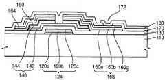
図1は、本発明の一実施例による薄膜トランジスタ基板の平面図であり、図2は、図1のI−I’に沿って見た断面図である。 FIG. 1 is a plan view of a thin film transistor substrate according to an embodiment of the present invention, and FIG. 2 is a cross-sectional view taken along line I-I 'of FIG.
図1及び図2を参照すると、本発明の一実施例による薄膜トランジスタ基板100は、絶縁基板110、ゲート配線120、ゲート絶縁膜130、活性層140、酸化防止層150、及びデータ配線160を含む。 1 and 2, the thin film transistor substrate 100 according to an embodiment of the present invention includes an
絶縁基板110は、光が透過される透明な物質からなる。一例として、絶縁基板110はガラスからなる。 The
ゲート配線120は、絶縁基板110上に形成され、ゲートライン122及びゲートライン122に接続されたゲート電極124を含む。ゲートライン122は横方向に延びている。ゲート電極124はゲートライン122に接続され、薄膜トランジスタ(TFT)のゲート電極124に該当する。 The
ゲートライン122及びゲート電極124を含むゲート配線120は、第1ゲート配線層120a、第2ゲート配線層120b及び第3ゲート配線層120cが順次積層された3層膜構造を有する。 The
第1ゲート配線層120aは、インジウム(In)を含む酸化物からなる。例えば、第1ゲート配線層120aは、インジウムスズ酸化物(以下、ITO)またはインジウム亜鉛酸化物(以下、IZO)からなる。第1ゲート配線層120aは、絶縁基板110との接着力を向上させるために形成する層であって、約50nm以下の厚さで形成されることが望ましい。 The first
第2ゲート配線層120bは、銀(Ag)または銀(Ag)を含む合金からなる。第2ゲート配線層120bは、配線の本来機能である電気信号の通路の役割を果たす層であって、比抵抗が低い銀または銀合金で形成される。 The second
第3ゲート配線層120cは、第1ゲート配線層120aと同一にインジウム(In)を含む酸化物からなる。例えば、第3ゲート配線層120cは、ITOまたはIZOからなる。第3ゲート配線層120cは、第2ゲート配線層120bを保護するために形成する層であって、後に続く工程で用いられるエッチング剤に強い物質からなる。 The third
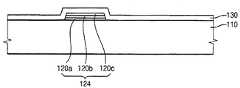
ゲート絶縁膜130は、ゲート配線120を覆うように絶縁基板110上に形成される。ゲート絶縁膜130は、例えば、シリコン窒化膜(SiNx)またはシリコン酸化膜(SiOx)からなる。 The
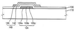
活性層140は、ゲート電極124と対応してゲート絶縁膜130上に形成される。活性層140は、半導体層142及びオーミックコンタクト層144を含む。例えば、半導体層142は、非晶質シリコン(以下、「a−Si」と言う。)からなる。オーミックコンタクト層144は、n型不純物が高濃度でドープされた非晶質シリコン(以下、「n+a−Si」と言う。)で構成される。オーミックコンタクト層144は、ソース電極164及びドレイン電極166と重なる領域に形成される。 The
酸化防止層150は、活性層140上に形成される。即ち、酸化防止層150は、n+a−Siからなるオーミックコンタクト層144の上部に形成される。酸化防止層150は、上部に形成されるソース電極164及びドレイン電極166に含まれている酸素がオーミックコンタクト144に含まれたシリコン(Si)と結合することを防止し、薄膜トランジスタ(TFT)の駆動特性を向上させる。 The
本実施例で、酸化防止層150は、シリサイド層で構成される。シリサイド層は、オーミックコンタクト層144上に金属膜を蒸着して形成し、シリサイド層の形成の後、シリサイド層を除いた金属膜はエッチング工程によって除去される。シリサイド層を形成する金属としては、チタン(Ti)、クロム(Cr)、モリブデン(Mo)、ニケル(Ni)、タンタル(Ta)、コバルト(Co)、マグネシウム(Mg)、バナジウム(V)、及びタングステン(W)などの金属またはこれらの合金が挙げられる。金属膜の除去は、乾式エッチング工程または湿式エッチング工程によって行われる。このように形成された酸化防止層150の厚さは約1nm〜500nmの範囲を有する。 In this embodiment, the
データ配線160は、ゲート絶縁膜130及び酸化防止層150上に形成される。データ配線160は、データライン162、ソース電極164及びドレイン電極166を含む。データライン162は、ゲート絶縁膜130上にゲートライン122と交差するように形成される。ソース電極164はデータライン162に接続され、酸化防止層150の上部にまで延びるように形成される。ドレイン電極166は、ソース電極164と離隔され、ゲート電極124を中心としてソース電極164の反対側である酸化防止層150の上部に形成される。ソース電極164は、薄膜トランジスタ(TFT)のソース電極164に該当し、ドレイン電極166は、薄膜トランジスタ(TFT)のドレイン電極166に該当する。 The
データライン162、ソース電極164、及びドレイン電極166を含むデータ配線160は、第1データ配線160a、第2データ配線層160b、及び第3データ配線層160cが順次に積層された3層膜構造を有する。 The
第1データ配線160aは、インジウム(In)を含む酸化物からなる。例えば、第1データ配線層160aは、ITOまたはIZOからなる。第1データ配線層160aは、ゲート絶縁膜130及び酸化防止層150との接着力を向上させるために形成する層であって、約50nm以下の厚さに形成されることが望ましい。 The
第2データ配線層160bは、銀または銀(Ag)を含む合金からなる。第2データ配線層160bは、配線が本来有する機能である電気信号の通路の役割を果たす層であって、比抵抗が低い銀または銀合金で形成する。 The second
第3データ配線層160cは、第1データ配線層160aと同一にインジウムを含む酸化物からなる。例えば、第3データ配線層160cは、ITOまたはIZOからなる。第3データ配線層160cは、第2データ配線層160bを保護するために形成する層であって、後に続く工程で用いられるエッチング剤に強い物質で形成される。特に、保護膜170にコンタクトホール172を形成するときに用いるエッチング剤やエッチング方法に強い物質で構成される。 The third
一方、薄膜トランジスタ基板100は、保護膜170及び画素電極180を更に含む。 Meanwhile, the thin film transistor substrate 100 further includes a
保護膜170は、データ配線160及びゲート絶縁膜130を覆うように絶縁基板110上に全面的に形成される。保護膜170には、ドレイン電極166を露出させるためのコンタクトホール172が形成される。 The
画素電極180は、保護膜170上に形成され、コンタクトホール172を通してドレイン電極166と電気的に接続される。画素電極180は、光が透過する透明な導電性物質からなる。例えば、画素電極180は、ITOまたはIZOからなる。 The
表1は、酸化防止層150のある場合と酸化防止層150のない場合の薄膜トランジスタ基板100の駆動特性を測定した測定データである。表1で、実験例は本実施例のように、酸化防止層が形成され、ゲート配線及びデータ配線は、ITO/Ag/ITOの3層膜構造を有する。反面、比較例1は、酸化防止層がなく、ゲート配線及びデータ配線は、ITO/Ag/ITOの3層膜構造を有する。比較例2は、酸化防止層がなく、ゲート配線及びデータ配線は、モリブデン(Mo)/アルミニウム(Al)/モリブデン(Mo)の3層膜構造を有する。 Table 1 shows measurement data obtained by measuring the driving characteristics of the thin film transistor substrate 100 with and without the

表1を参照すると、ITO/Ag/ITOの3層膜構造を有する実験例は、酸化防止層なしにITO/Ag/ITOの3層膜構造を有する比較例1に比べて薄膜トランジスタのオン電流(Ion)が増加し、オフ電流(Ioff)が減少する。実験例は、従来の酸化防止層なしにMo/Al/Moの3層膜構造を有する比較例2と比較してほぼ同一の水準のオン電流(Ion)及びオフ電流(Ioff)を有する。Referring to Table 1, an experimental example having a three-layer structure of ITO / Ag / ITO has a thin film transistor on-current (compared with Comparative Example 1 having a three-layer structure of ITO / Ag / ITO without an antioxidant layer). Ion ) increases and off-current (Ioff ) decreases. The experimental example has almost the same level of on-current (Ion ) and off-current (Ioff ) as compared with the comparative example 2 having a three-layer structure of Mo / Al / Mo without a conventional antioxidant layer. .
反面、実験例におけるデータ配線抵抗(Rd)は、比較例2に比べて低くなることがわかる。したがって、本発明の一実施例による薄膜トランジスタ基板は、従来のMo/Al/Moの3層膜構造を有する薄膜トランジスタ基板とほぼ同一の水準の駆動特性を有する反面、配線抵抗は顕著に減少することがわかる。On the other hand, it can be seen that the data wiring resistance (Rd ) in the experimental example is lower than that in Comparative Example 2. Accordingly, the thin film transistor substrate according to the embodiment of the present invention has substantially the same level of driving characteristics as the thin film transistor substrate having the conventional three-layer structure of Mo / Al / Mo, but the wiring resistance is remarkably reduced. Recognize.
以下、本発明の一実施例による薄膜トランジスタ基板の製造方法に対して図3乃至図10を参照して詳細に説明する。 Hereinafter, a method of manufacturing a thin film transistor substrate according to an embodiment of the present invention will be described in detail with reference to FIGS.
図3乃至図10は、図2に示した薄膜トランジスタ基板の製造過程を示した工程図である。3 to 10 are process diagrams showing a manufacturing process of the thin film transistor substrate shown in FIG.
図3及び図4を参照すると、絶縁基板110上に第1ゲート配線層120a、第2ゲート配線層120b及び第3ゲート配線層120cを次第に積層し、フォトリソグラフィ工程を通じてゲートライン122及びゲート電極124を含むゲート配線120を形成する。3 and 4, the first
第1ゲート配線層120aは、絶縁基板110との接着性を向上させるためにインジウム(In)を含む酸化物からなる。例えば、第1ゲート配線層120aはITOまたはIZOからなる。第1ゲート配線層(120a)は、約50nm以下の厚さに形成される。 The first
第2ゲート配線層120bは、比抵抗が低い銀(Ag)または銀を含む合金からなる。 The second
第3ゲート配線層120cは、第2ゲート配線層120bを保護するためにインジウム(In)を含む酸化物からなる。例えば、第3ゲート配線層120cは、ITOまたはIZOからなる。第3ゲート配線層120cは、約10nm以下の厚さに形成される。 The third
図5を参照すると、ゲート配線120が形成された絶縁基板110上にシリコン窒化膜(SiNx)またはシリコン酸化膜(SiOx)からなるゲート絶縁膜130を形成する。 Referring to FIG. 5, a
図6及び図7を参照すると、ゲート絶縁膜130上に半導体層142及びオーミックコンタクト層144を次第に積層し、フォトリソグラフィ工程を通してゲート電極124と重なるように活性層140を形成する。半導体層142は、a−Siからなり、オーミックコンタクト層144は、n型不純物が高濃度にドープされたn+a−Siからなる。 6 and 7, a
図8を参照すると、活性層140及びゲート絶縁膜130上にスパッタリング方式を用いて金属膜152を蒸着する。金属膜152は、シリコン(Si)と結合してシリサイドが形成可能な金属からなる。例えば、金属膜152は、チタン(Ti)、クロム(Cr)、モリブデン(Mo)、ニケル(Ni)、タンタル(Ta)、コバルト(Co)、マグネシウム(Mg)、バナジウム(V)、及びタングステン(W)などの金属またはこれらの合金からなる。 Referring to FIG. 8, a
金属膜152に含まれた金属はn+a−Siからなるオーミックコンタクト層144に含まれたシリコン(Si)と結合して酸化防止層150を形成する。本実施例で、酸化防止層150は、シリコン(Si)と金属が結合されたシリサイド層で構成される。酸化防止層150は、上部に形成されるソース電極164及びドレイン電極166に含まれている酸素がオーミックコンタクト層144に含まれたシリコン(Si)と結合することを防止して薄膜トランジスタ(TFT)の駆動特性を向上させる。 The metal contained in the
一方、酸化防止層150の形成のために金属膜152を熱処理する工程を追加してもよい。例えば、熱処理工程は、約500℃以下で、約1時間以内に進行する。このように形成された酸化防止層150の厚さは約1nm〜約500nmの範囲にある。 On the other hand, a process of heat-treating the
酸化防止層150の形成の後、エッチング工程によって金属膜152を除去する。金属膜152を除去するためのエッチング工程は、乾式エッチング工程または湿式エッチング工程によって行われる。金属膜152の除去の後には、酸化防止層150のみがオーミックコンタクト層144上に残るようになる。 After the formation of the
図9及び図10を参照すると、ゲート絶縁膜130及び酸化防止層150上に第1データ配線層160a、第2データ配線層160b及び第3データ配線層160cを次第に積層し、フォトリソグラフィ工程によってデータライン162、ソース電極164及びドレイン電極166を含むデータ配線160を形成する。データライン162は、ゲート絶縁膜130上にゲートライン122と交差するように形成される。ソース電極164はデータライン162に接続され、酸化防止層150の上部にまで延びるように形成される。ドレイン電極166は、ソース電極164と離隔され、ゲート電極124を中心としてソース電極164の反対側である酸化防止層150の上部に形成される。 Referring to FIGS. 9 and 10, the first
第1データ配線層160aは、ゲート絶縁膜130及び酸化防止層150との接着性を向上させるために、インジウム(In)を含む酸化物からなる。例えば、第1データ配線層160aは、ITOまたはIZOからなる。第1データ配線層160aは、約50nm以下の厚さに形成される。 The first
第2データ配線層160bは、比抵抗が低い銀(Ag)または銀を含む合金からなる。 The second
第3データ配線層160cは、第2データ配線層160bを保護するためにインジウムを含む酸化物からなる。例えば、第3データ配線層160cは、ITOまたはIZOからなる。第3データ配線層160cは、約10nm以下の厚さに形成される。 The third
その後、データ配線160でカバーしない酸化防止層150及びオーミックコンタクト層144をエッチングし、オーミックコンタクト層144をゲート電極124を中心として両側に分離する一方、半導体層142を露出させる。 Thereafter, the
図1及び図2を参照すると、データ配線160及びゲート絶縁膜130上に無機絶縁膜からなる保護膜170を形成する。その後、フォトリソグラフィ工程によって保護膜170をパターニングしてドレイン電極166を露出するためのコンタクトホール172を形成する。コンタクトホール172は、角を有する形状または円形状に形成することができる。 Referring to FIGS. 1 and 2, a
その後、保護膜170上に透明な導電層(図示せず)を蒸着し、フォトリソグラフィ工程によって画素電極180を形成する。画素電極180は、コンタクトホール172を通してドレイン電極166と電気的に接続される。画素電極180は、光が透過可能な透明な導電性物質からなる。例えば、画素電極180は、ITOまたはIZOからなる。 Thereafter, a transparent conductive layer (not shown) is deposited on the
一方、本実施例では、ゲート配線及びデータ配線が全て3層膜構造を有するか、必要に応じてゲート配線とデータ配線のいずれか一つのみが3層膜構造を有してもよい。 On the other hand, in this embodiment, the gate wiring and the data wiring all have a three-layer film structure, or only one of the gate wiring and the data wiring may have a three-layer film structure as necessary.
このような薄膜トランジスタ及びこれの製造方法によると、ゲート配線及びデータや配線をインジウム酸化物、銀及びインジウム酸化物からなる3層膜構造で形成することで、配線抵抗を減少させることができる。 According to such a thin film transistor and a manufacturing method thereof, the wiring resistance can be reduced by forming the gate wiring, the data, and the wiring with a three-layer film structure made of indium oxide, silver, and indium oxide.
また、オーミックコンタクト層とデータ配線との間にシリサイドからなる酸化防止層を形成することによって、薄膜トランジスタのオン電流(Ion)を増加させ、オフ電流(Ioff)を減少させて薄膜トランジスタの駆動特性を向上させることができる。Further, by forming an anti-oxidation layer made of silicide between the ohmic contact layer and the data wiring, the on-current (Ion ) of the thin film transistor is increased, and the off-current (Ioff ) is decreased to drive the thin film transistor. Can be improved.
以上、本発明の実施例によって詳細に説明したが、本発明はこれに限定されず、本発明が属する技術分野において通常の知識を有するものであれば本発明の思想と精神を離脱することなく、本発明を修正または変更できる。 As described above, the embodiments of the present invention have been described in detail. However, the present invention is not limited to these embodiments, and any person who has ordinary knowledge in the technical field to which the present invention belongs can be used without departing from the spirit and spirit of the present invention. The present invention can be modified or changed.
100 薄膜トランジスタ基板
110 絶縁基板
120 ゲート配線
122 ゲートライン
124 ゲート電極
130 ゲート絶縁膜
140 活性層
142 アクティブ層
144 オーミックコンタクト層
150 酸化防止層
160 データ配線
160a 第1データ配線層
160b 第2データ配線層
160c 第3データ配線層
162 データライン
164 ソース電極
166 ドレイン電極
170 保護膜
180 画素電極
100 Thin
Claims (23)
Translated fromJapanese前記絶縁基板上に形成され、ゲートライン及び前記ゲートラインと接続されたゲート電極を含むゲート配線と、
前記ゲート配線を覆うゲート絶縁膜と、
前記ゲート電極と対応して前記ゲート絶縁膜上に形成された活性層と、
前記活性層上に形成された酸化防止層と、
前記ゲート絶縁膜上に前記ゲートラインと交差するように形成されたデータライン、前記データラインに接続され前記酸化防止層上に形成されたソース電極、及び前記ソース電極と離隔されて前記酸化防止層上に形成されたドレイン電極を含むデータ配線と、
前記データ配線を覆い、前記ドレイン電極を露出させるコンタクトホールを有する保護膜と、
前記保護膜上に形成され、前記コンタクトホールを通して前記ドレイン電極と接続される画素電極と、を含むことを特徴とする薄膜トランジスタ基板。An insulating substrate;
A gate wiring formed on the insulating substrate and including a gate line and a gate electrode connected to the gate line;
A gate insulating film covering the gate wiring;
An active layer formed on the gate insulating film corresponding to the gate electrode;
An antioxidant layer formed on the active layer;
A data line formed on the gate insulating film so as to intersect the gate line, a source electrode connected to the data line and formed on the antioxidant layer, and the antioxidant layer separated from the source electrode A data line including a drain electrode formed thereon;
A protective film covering the data wiring and having a contact hole exposing the drain electrode;
A thin film transistor substrate comprising: a pixel electrode formed on the protective film and connected to the drain electrode through the contact hole.
インジウム酸化物からなる第1データ配線層と、
前記第1データ配線層上に形成され、銀(Ag)からなる第2データ配線層と、
前記第2データ配線層上に形成され、インジウム酸化物からなる第3データ配線層と、を含むことを特徴とする請求項1記載の薄膜トランジスタ基板。The data wiring is
A first data wiring layer made of indium oxide;
A second data wiring layer formed on the first data wiring layer and made of silver (Ag);
The thin film transistor substrate according to claim 1, further comprising: a third data wiring layer formed on the second data wiring layer and made of indium oxide.
インジウム酸化物からなる第1ゲート配線層と、
前記第1ゲート配線層上に形成され、銀(Ag)からなる第2ゲート配線層と、
前記第2ゲート配線層上に形成され、インジウム酸化物からなる第3ゲート配線層と、を含むことを特徴とする請求項1記載の薄膜トランジスタ基板。The gate wiring is
A first gate wiring layer made of indium oxide;
A second gate wiring layer formed on the first gate wiring layer and made of silver (Ag);
2. The thin film transistor substrate according to claim 1, further comprising a third gate wiring layer formed on the second gate wiring layer and made of indium oxide.
非晶質シリコンからなる半導体層と、
前記半導体層上に形成され、n型不純物が高濃度でドープされた非晶質シリコンからなるオーミックコンタクト層と、を含むことを特徴とする請求項1記載の薄膜トランジスタ基板。The active layer is
A semiconductor layer made of amorphous silicon;
2. The thin film transistor substrate according to claim 1, further comprising an ohmic contact layer formed on the semiconductor layer and made of amorphous silicon doped with an n-type impurity at a high concentration.
前記絶縁基板上に形成され、ゲートライン及び前記ゲートラインに接続されたゲート電極を含むゲート配線と、
前記ゲート配線を覆うゲート絶縁膜と、
前記ゲート電極と対応して前記ゲート絶縁膜上に形成された活性層と、
前記活性層上に形成されたシリサイド層と、
前記ゲート絶縁膜上に前記ゲートラインと交差するように形成されたデータラインと、前記データラインに接続され前記シリサイド層上に形成されたソース電極、及び前記ソース電極と離隔されて前記シリサイド層上に形成されたドレイン電極を含み、インジウム酸化物、銀、及びインジウム酸化物が順次積層された3層膜構造を有するデータ配線と、
前記データ配線を覆い、前記ドレイン電極を露出させるコンタクトホールを有する保護膜と、
前記保護膜上に形成され、前記コンタクトホールを通して前記ドレイン電極と接続される画素電極と、を含むことを特徴とする薄膜トランジスタ基板。An insulating substrate;
A gate line formed on the insulating substrate and including a gate line and a gate electrode connected to the gate line;
A gate insulating film covering the gate wiring;
An active layer formed on the gate insulating film corresponding to the gate electrode;
A silicide layer formed on the active layer;
A data line formed on the gate insulating film so as to intersect the gate line, a source electrode connected to the data line and formed on the silicide layer, and spaced apart from the source electrode on the silicide layer A data wiring having a three-layer film structure including a drain electrode formed on the substrate and sequentially stacking indium oxide, silver, and indium oxide;
A protective film covering the data wiring and having a contact hole exposing the drain electrode;
A thin film transistor substrate comprising: a pixel electrode formed on the protective film and connected to the drain electrode through the contact hole.
前記ゲート配線を覆うゲート絶縁膜を形成し、
前記ゲート電極と対応して前記ゲート絶縁膜上に活性層を形成し、
前記活性層上に酸化防止層を形成し、
前記ゲートラインと交差するデータライン、前記データラインに接続され前記酸化防止層上に配置されるソース電極、及び前記ソース電極と離隔されて前記酸化防止層上に配置されるドレイン電極を含むデータ配線を形成すること、を含むことを特徴とする薄膜トランジスタ基板の製造方法。Forming a gate line including a gate line and a gate electrode connected to the gate line on an insulating substrate;
Forming a gate insulating film covering the gate wiring;
Forming an active layer on the gate insulating film corresponding to the gate electrode;
Forming an antioxidant layer on the active layer;
A data line including a data line intersecting with the gate line, a source electrode connected to the data line and disposed on the antioxidant layer, and a drain electrode spaced apart from the source electrode and disposed on the antioxidant layer Forming a thin film transistor substrate, comprising: forming a thin film transistor substrate.
前記活性層上に金属膜を蒸着して前記酸化防止層を形成し、
前記酸化防止層が残るように前記金属膜をエッチングすること、を含むことを特徴とする請求項12記載の薄膜トランジスタ基板の製造方法。Forming the antioxidant layer includes
Depositing a metal film on the active layer to form the antioxidant layer;
13. The method of manufacturing a thin film transistor substrate according to claim 12, comprising etching the metal film so that the antioxidant layer remains.
インジウム酸化物からなる第1データ配線層と、
前記第1データ配線層上に形成され、銀(Ag)からなる第2データ配線層と、
前記第2データ配線層上に形成され、インジウム酸化物からなる第3データ配線層と、を含むことを特徴とする請求項12記載の薄膜トランジスタ基板の製造方法。The data wiring is
A first data wiring layer made of indium oxide;
A second data wiring layer formed on the first data wiring layer and made of silver (Ag);
13. The method of manufacturing a thin film transistor substrate according to claim 12, further comprising a third data wiring layer formed on the second data wiring layer and made of indium oxide.
インジウム酸化物からなる第1ゲート配線層と、
前記第1ゲート配線層上に形成され、銀(Ag)からなる第2ゲート配線層と、
前記第2ゲート配線層上に形成され、インジウム酸化物からなる第3ゲート配線層と、を含むことを特徴とする請求項18記載の薄膜トランジスタ基板の製造方法。The gate wiring is
A first gate wiring layer made of indium oxide;
A second gate wiring layer formed on the first gate wiring layer and made of silver (Ag);
19. The method of manufacturing a thin film transistor substrate according to claim 18, further comprising: a third gate wiring layer formed on the second gate wiring layer and made of indium oxide.
非晶質シリコンからなる半導体層と、
前記半導体層上に形成され、n型不純物が高濃度でドープされた非晶質シリコンからなるオーミックコンタクト層と、を含むことを特徴とする請求項12記載の薄膜トランジスタ基板の製造方法。The active layer is
A semiconductor layer made of amorphous silicon;
13. The method of manufacturing a thin film transistor substrate according to claim 12, further comprising an ohmic contact layer formed on the semiconductor layer and made of amorphous silicon doped with an n-type impurity at a high concentration.
前記保護膜をパターニングして前記ドレイン電極を露出させるコンタクトホールを形成し、
前記コンタクトホールを通して前記ドレイン電極に接続される画素電極を形成すること、を更に含むことを特徴とする請求項12記載の薄膜トランジスタ基板の製造方法。
Forming a protective film covering the data wiring;
Patterning the protective film to form a contact hole exposing the drain electrode;
The method of manufacturing a thin film transistor substrate according to claim 12, further comprising forming a pixel electrode connected to the drain electrode through the contact hole.
Priority Applications (1)
| Application Number | Priority Date | Filing Date | Title |
|---|---|---|---|
| JP2006071890AJP2007250804A (en) | 2006-03-15 | 2006-03-15 | Thin film transistor substrate and manufacturing method thereof |
Applications Claiming Priority (1)
| Application Number | Priority Date | Filing Date | Title |
|---|---|---|---|
| JP2006071890AJP2007250804A (en) | 2006-03-15 | 2006-03-15 | Thin film transistor substrate and manufacturing method thereof |
Publications (2)
| Publication Number | Publication Date |
|---|---|
| JP2007250804Atrue JP2007250804A (en) | 2007-09-27 |
| JP2007250804A5 JP2007250804A5 (en) | 2009-04-30 |
Family
ID=38594776
Family Applications (1)
| Application Number | Title | Priority Date | Filing Date |
|---|---|---|---|
| JP2006071890AWithdrawnJP2007250804A (en) | 2006-03-15 | 2006-03-15 | Thin film transistor substrate and manufacturing method thereof |
Country Status (1)
| Country | Link |
|---|---|
| JP (1) | JP2007250804A (en) |
Cited By (11)
| Publication number | Priority date | Publication date | Assignee | Title |
|---|---|---|---|---|
| KR20100092885A (en)* | 2009-02-13 | 2010-08-23 | 가부시키가이샤 한도오따이 에네루기 켄큐쇼 | Transistor, semiconductor device including the transistor, and manufacturing method of the transistor and the semiconductor device |
| KR101065317B1 (en)* | 2009-11-13 | 2011-09-16 | 삼성모바일디스플레이주식회사 | Organic light emitting display and manufacturing method thereof |
| US8198657B2 (en) | 2009-09-21 | 2012-06-12 | Samsung Electronics Co., Ltd. | Thin film transistor array panel and method for manufacturing the same |
| JP2012159767A (en)* | 2011-02-02 | 2012-08-23 | Japan Display Central Co Ltd | Array substrate for display device, and display device |
| KR20130020288A (en)* | 2011-08-19 | 2013-02-27 | 엘지디스플레이 주식회사 | Thin film transistor substrate and method of fabricating the same |
| KR20160035171A (en)* | 2014-09-22 | 2016-03-31 | 엘지디스플레이 주식회사 | Organic light emitting diode display device |
| KR101733758B1 (en) | 2009-02-13 | 2017-05-08 | 가부시키가이샤 한도오따이 에네루기 켄큐쇼 | Transistor, semiconductor device including the transistor, and manufacturing method of the transistor and the semiconductor device |
| US9899531B2 (en) | 2014-08-05 | 2018-02-20 | Samsung Display Co., Ltd. | Thin film transistor substrate, method of manufacturing the same, and display apparatus having the same |
| KR20180021033A (en)* | 2008-12-25 | 2018-02-28 | 가부시키가이샤 한도오따이 에네루기 켄큐쇼 | Semiconductor device and manufacturing method thereof |
| US10615179B2 (en) | 2010-02-05 | 2020-04-07 | Semiconductor Energy Laboratory Co., Ltd. | Semiconductor device and method for manufacturing the same |
| CN112259611A (en)* | 2020-10-12 | 2021-01-22 | 昆山龙腾光电股份有限公司 | Oxide semiconductor thin film transistor and manufacturing method thereof |
- 2006
- 2006-03-15JPJP2006071890Apatent/JP2007250804A/ennot_activeWithdrawn
Cited By (27)
| Publication number | Priority date | Publication date | Assignee | Title |
|---|---|---|---|---|
| US11158654B2 (en) | 2008-12-25 | 2021-10-26 | Semiconductor Energy Laboratory Co., Ltd. | Semiconductor device and manufacturing method thereof |
| KR102165978B1 (en)* | 2008-12-25 | 2020-10-15 | 가부시키가이샤 한도오따이 에네루기 켄큐쇼 | Semiconductor device and manufacturing method thereof |
| US10720451B2 (en) | 2008-12-25 | 2020-07-21 | Semiconductor Energy Laboratory Co., Ltd. | Semiconductor device and manufacturing method thereof |
| KR102132155B1 (en)* | 2008-12-25 | 2020-07-09 | 가부시키가이샤 한도오따이 에네루기 켄큐쇼 | Semiconductor device and manufacturing method thereof |
| US11996416B2 (en) | 2008-12-25 | 2024-05-28 | Semiconductor Energy Laboratory Co., Ltd. | Semiconductor device and manufacturing method thereof |
| US10483290B2 (en) | 2008-12-25 | 2019-11-19 | Semiconductor Energy Laboratory Co., Ltd. | Semiconductor device and manufacturing method thereof |
| KR20180021033A (en)* | 2008-12-25 | 2018-02-28 | 가부시키가이샤 한도오따이 에네루기 켄큐쇼 | Semiconductor device and manufacturing method thereof |
| KR20190018657A (en)* | 2008-12-25 | 2019-02-25 | 가부시키가이샤 한도오따이 에네루기 켄큐쇼 | Semiconductor device and manufacturing method thereof |
| KR20100092885A (en)* | 2009-02-13 | 2010-08-23 | 가부시키가이샤 한도오따이 에네루기 켄큐쇼 | Transistor, semiconductor device including the transistor, and manufacturing method of the transistor and the semiconductor device |
| KR101635624B1 (en) | 2009-02-13 | 2016-07-04 | 가부시키가이샤 한도오따이 에네루기 켄큐쇼 | Transistor, semiconductor device including the transistor, and manufacturing method of the transistor and the semiconductor device |
| KR101733758B1 (en) | 2009-02-13 | 2017-05-08 | 가부시키가이샤 한도오따이 에네루기 켄큐쇼 | Transistor, semiconductor device including the transistor, and manufacturing method of the transistor and the semiconductor device |
| US8198657B2 (en) | 2009-09-21 | 2012-06-12 | Samsung Electronics Co., Ltd. | Thin film transistor array panel and method for manufacturing the same |
| US8395160B2 (en) | 2009-11-13 | 2013-03-12 | Samsung Display Co., Ltd. | Organic light emitting display apparatus and method of manufacturing the same |
| KR101065317B1 (en)* | 2009-11-13 | 2011-09-16 | 삼성모바일디스플레이주식회사 | Organic light emitting display and manufacturing method thereof |
| US11469255B2 (en) | 2010-02-05 | 2022-10-11 | Semiconductor Energy Laboratory Co., Ltd. | Semiconductor device and method for manufacturing the same |
| US11749686B2 (en) | 2010-02-05 | 2023-09-05 | Semiconductor Energy Laboratory Co., Ltd. | Semiconductor device and method for manufacturing the same |
| US10615179B2 (en) | 2010-02-05 | 2020-04-07 | Semiconductor Energy Laboratory Co., Ltd. | Semiconductor device and method for manufacturing the same |
| US11101295B2 (en) | 2010-02-05 | 2021-08-24 | Semiconductor Energy Laboratory Co., Ltd. | Semiconductor device and method for manufacturing the same |
| US12113074B2 (en) | 2010-02-05 | 2024-10-08 | Semiconductor Energy Laboratory Co., Ltd. | Semiconductor device and method for manufacturing the same |
| JP2012159767A (en)* | 2011-02-02 | 2012-08-23 | Japan Display Central Co Ltd | Array substrate for display device, and display device |
| KR101938627B1 (en)* | 2011-08-19 | 2019-01-16 | 엘지디스플레이 주식회사 | Thin film transistor substrate and method of fabricating the same |
| KR20130020288A (en)* | 2011-08-19 | 2013-02-27 | 엘지디스플레이 주식회사 | Thin film transistor substrate and method of fabricating the same |
| US10128382B2 (en) | 2014-08-05 | 2018-11-13 | Samsung Display Co., Ltd. | Thin film transistor substrate, method of manufacturing the same, and display apparatus having the same |
| US9899531B2 (en) | 2014-08-05 | 2018-02-20 | Samsung Display Co., Ltd. | Thin film transistor substrate, method of manufacturing the same, and display apparatus having the same |
| KR102254524B1 (en) | 2014-09-22 | 2021-05-21 | 엘지디스플레이 주식회사 | Organic light emitting diode display device |
| KR20160035171A (en)* | 2014-09-22 | 2016-03-31 | 엘지디스플레이 주식회사 | Organic light emitting diode display device |
| CN112259611A (en)* | 2020-10-12 | 2021-01-22 | 昆山龙腾光电股份有限公司 | Oxide semiconductor thin film transistor and manufacturing method thereof |
Similar Documents
| Publication | Publication Date | Title |
|---|---|---|
| JP2007250804A (en) | Thin film transistor substrate and manufacturing method thereof | |
| JP6261845B2 (en) | Thin film transistor array panel and manufacturing method thereof | |
| JP5324111B2 (en) | Thin film transistor array panel and manufacturing method thereof | |
| US7741641B2 (en) | TFT substrate and display device having the same | |
| JP5215543B2 (en) | Thin film transistor substrate | |
| US7336324B2 (en) | Array substrate for liquid crystal display device and fabricating method thereof | |
| KR101431136B1 (en) | Method of manufacturing thin film transistor substrate | |
| US20150295092A1 (en) | Semiconductor device | |
| US11215891B2 (en) | Active matrix substrate and manufacturing method thereof | |
| KR102380647B1 (en) | Thin film transistor array panel and manufacturing method thereof | |
| KR101353269B1 (en) | Thin film transistor substrate and method for manufacturing the same | |
| US9024311B2 (en) | Thin film transistor, method for manufacturing same, active matrix substrate, display panel and display device | |
| US20120199891A1 (en) | Semiconductor device and method for manufacturing same | |
| US20210249445A1 (en) | Active matrix substrate and method for manufacturing same | |
| WO2014146380A1 (en) | Thin film transistor and manufacturing method therefor, array substrate, and display apparatus | |
| JP2007053363A5 (en) | ||
| TW201417268A (en) | Thin film transistor array panel and organic light emitting diode display therewith | |
| CN103915451B (en) | A kind of array base palte and manufacture method thereof, display unit | |
| KR20150034947A (en) | Metal wire, thin-film transistor substrate and method for manufacturing a thin-film transistor substrate | |
| KR20130117558A (en) | Thin film transistor, thin film transistor array panel and manufacturing method for a thin film transistor array panel | |
| JP2007073562A (en) | Thin-film transistor | |
| WO2012169397A1 (en) | Thin-film transistor, method for producing same, and display element | |
| JP2019169606A (en) | Active matrix substrate and method of manufacturing the same | |
| KR20070109192A (en) | Display substrate, manufacturing method thereof and display device having same | |
| TW201220506A (en) | Thin film transistor, method for manufacturing the same, and display device using the same |
Legal Events
| Date | Code | Title | Description |
|---|---|---|---|
| A521 | Written amendment | Free format text:JAPANESE INTERMEDIATE CODE: A523 Effective date:20090312 | |
| A621 | Written request for application examination | Free format text:JAPANESE INTERMEDIATE CODE: A621 Effective date:20090312 | |
| A761 | Written withdrawal of application | Free format text:JAPANESE INTERMEDIATE CODE: A761 Effective date:20100513 |