JP2007242787A - Wafer division method - Google Patents
Wafer division methodDownload PDFInfo
- Publication number
- JP2007242787A JP2007242787AJP2006061088AJP2006061088AJP2007242787AJP 2007242787 AJP2007242787 AJP 2007242787AJP 2006061088 AJP2006061088 AJP 2006061088AJP 2006061088 AJP2006061088 AJP 2006061088AJP 2007242787 AJP2007242787 AJP 2007242787A
- Authority
- JP
- Japan
- Prior art keywords
- wafer
- holding
- suction
- back surface
- along
- Prior art date
- Legal status (The legal status is an assumption and is not a legal conclusion. Google has not performed a legal analysis and makes no representation as to the accuracy of the status listed.)
- Pending
Links
Images


Landscapes
- Dicing (AREA)
- Container, Conveyance, Adherence, Positioning, Of Wafer (AREA)
Abstract
Translated fromJapaneseDescription
Translated fromJapanese本発明は、表面に複数の分割予定ラインが格子状に形成されているウエーハを、該分割予定ラインに沿って個々のチップに分割するウエーハの分割方法に関する。 The present invention relates to a wafer dividing method for dividing a wafer having a plurality of division lines formed on a surface thereof in a lattice shape into individual chips along the division lines.
半導体デバイス製造工程においては、略円板形状である半導体ウエーハの表面に格子状に配列されたストリートと呼ばれる分割予定ラインによって複数の領域が区画され、この区画された領域にIC、LSI等のデバイスを形成する。そして、半導体ウエーハを分割予定ラインに沿って切断することによりデバイスが形成された領域を分割して個々の半導体チップを製造している。また、サファイヤ基板の表面に窒化ガリウム系化合物半導体等が積層された光デバイスウエーハも所定の分割予定ラインに沿って切断することにより個々の発光ダイオード、レーザーダイオード等の光デバイスに分割され、電気機器に広く利用されている。 In the semiconductor device manufacturing process, a plurality of regions are partitioned by dividing lines called streets arranged in a lattice pattern on the surface of a substantially wafer-shaped semiconductor wafer, and devices such as ICs, LSIs, etc. are partitioned in the partitioned regions. Form. Then, the semiconductor wafer is cut along the planned dividing line to divide the region where the device is formed to manufacture individual semiconductor chips. In addition, an optical device wafer in which a gallium nitride compound semiconductor or the like is laminated on the surface of a sapphire substrate is also divided into optical devices such as individual light-emitting diodes and laser diodes by cutting along a predetermined division line. Widely used.
上述した半導体ウエーハや光デバイスウエーハ等を分割予定ラインに沿って分割する方法として、ウエーハに対して透過性を有する波長のパルスレーザー光線を用い、分割すべき領域の内部に集光点を合わせてパルスレーザー光線を照射するレーザー加工方法も試みられている。このレーザー加工方法を用いた分割方法は、ウエーハの裏面側から内部に集光点を合わせて被加工物に対して透過性を有する赤外光領域のパルスレーザー光線を照射し、ウエーハの内部に分割予定ラインに沿って変質層を連続的に形成し、この変質層が形成されることによって強度が低下した分割予定ラインに沿って外力を加えることにより、被加工物を分割するものである。(例えば、特許文献1参照。)
しかるに、分割予定ラインに沿って変質層が形成されたウエーハをレーザー加工装置のチャックテーブルから搬出する際に、ウエーハが変質層に沿って破断され、取り扱いが困難になるという問題がある。このような問題を解消するために、分割予定ラインに沿って変質層が形成されたウエーハの裏面全面を全面吸着パッドによって吸引保持してチャックテーブルから搬出し、後工程に搬送している。 However, when carrying out the wafer in which the deteriorated layer is formed along the planned dividing line from the chuck table of the laser processing apparatus, there is a problem that the wafer is broken along the deteriorated layer and is difficult to handle. In order to solve such a problem, the entire back surface of the wafer on which the deteriorated layer is formed along the planned division line is sucked and held by the entire suction pad, and is carried out of the chuck table and conveyed to the subsequent process.
而して、吸着パッドによって裏面全面を吸引保持して搬送したウエーハを変質層が形成された分割予定ラインに沿って個々のデバイス(チップ)に分割すると、抗折強度が低い(例えば400MPa以下) デバイス(チップ)が増える傾向があり、特に厚さが300μm以下の薄いウエーハにおいては問題となる。このような問題は、上記吸着パッドの吸引保持部が多孔質セラミックによって形成されているため、高度の高い多孔質セラミックからなる吸引保持部材にウエーハの裏面全面を吸引保持した際に、ウエーハの裏面に微細なクラックが生成されるためであると考えられる。 Thus, when the wafer conveyed by sucking and holding the entire back surface with the suction pad is divided into individual devices (chips) along the planned division line on which the altered layer is formed, the bending strength is low (for example, 400 MPa or less). There is a tendency for devices (chips) to increase, and this becomes a problem particularly in thin wafers having a thickness of 300 μm or less. Such a problem is that the suction holding portion of the suction pad is formed of porous ceramic, so that when the entire back surface of the wafer is sucked and held by a suction holding member made of highly porous ceramic, the back surface of the wafer This is probably because fine cracks are generated.
本発明は上記事実に鑑みてなされたものであり、その主たる技術的課題は、個々に分割されたチップの抗折強度を低下させることなく、ウエーハを分割することができるウエーハの分割方法を提供することである。 The present invention has been made in view of the above-mentioned facts, and its main technical problem is to provide a wafer dividing method capable of dividing a wafer without lowering the bending strength of the individually divided chips. It is to be.
上記主たる技術課題を解決するため、本発明によれば、表面に分割予定ラインが形成されたウエーハを、該分割予定ラインに沿って分割するウエーハの分割方法であって、
該ウエーハの表面に保護テープを貼着する保護テープ貼着工程と、
レーザー加工装置の被加工物を保持するチャックテーブルにウエーハの保護テープ側を保持するウエーハ保持工程と、
該チャックテーブルに保持されたウエーハに対して透過性を有する波長のレーザー光線をウエーハの裏面側から該分割予定ラインに沿って照射し、ウエーハの内部に該分割予定ラインに沿って変質層を形成する変質層形成工程と、
該変質層形成工程を実施した後に、吸着面に多孔質樹脂層を有する吸着パッドによって該チャックテーブルに保持されているウエーハの裏面を吸引保持し、該チャックテーブルからウエーハを搬出するウエーハ搬出工程と、
該吸着パッドに裏面が吸引保持されているウエーハの表面を保持するとともにウエーハの裏面から該吸着パッドを外し、ウエーハの裏面に環状のフレームに装着される粘着テープを貼着し、該粘着テープを介してウエーハを該環状のフレームに支持するウエーハ支持工程と、
該環状のフレームに該粘着テープを介して支持されたウエーハに外力を作用せしめることにより該変質層が形成された該分割予定ラインに沿ってウエーハを破断するウエーハ破断工程と、を含む、
ことを特徴とするウエーハの分割方法が提供される。In order to solve the above-mentioned main technical problem, according to the present invention, a wafer dividing method for dividing a wafer having a division planned line formed on a surface along the division planned line,
A protective tape attaching step of attaching a protective tape to the surface of the wafer;
A wafer holding step for holding the protective tape side of the wafer on a chuck table for holding a workpiece of the laser processing apparatus;
A laser beam having a wavelength that is transparent to the wafer held on the chuck table is irradiated from the back side of the wafer along the division line to form a deteriorated layer along the division line inside the wafer. An altered layer forming step;
A wafer unloading step of sucking and holding the back surface of the wafer held on the chuck table by a suction pad having a porous resin layer on the suction surface after carrying out the deteriorated layer forming step, and unloading the wafer from the chuck table; ,
While holding the front surface of the wafer whose back surface is sucked and held on the suction pad, the suction pad is removed from the back surface of the wafer, and an adhesive tape attached to an annular frame is attached to the back surface of the wafer. A wafer support step for supporting the wafer on the annular frame via,
A wafer breaking step of breaking the wafer along the division line in which the altered layer is formed by applying an external force to the wafer supported by the annular frame via the adhesive tape,
A method of dividing a wafer is provided.
上記ウエーハ搬出工程において用いる吸着パッドの吸着面を形成する多孔質樹脂層は、多孔質樹脂シートからなっている。 The porous resin layer forming the suction surface of the suction pad used in the wafer unloading step is made of a porous resin sheet.
本発明によるウエーハの分割方法においては、レーザー加工装置のチャックテーブルに保持され変質層形成工程が実施されたウエーハを搬出するウエーハ搬出工程は、吸着面に多孔質樹脂層を有する吸着パッドによってウエーハの裏面を吸引保持しチャックテーブルからウエーハを搬出するので、ウエーハの裏面に高度の高い多孔質セラミック等からなる吸引保持部が接触することはなく、ウエーハの裏面には多孔質樹脂層が接触するため、ウエーハの裏面に微細なクラックが生成されることはない。従って、ウエーハが分割された個々のチップの抗折強度が低下することはない。 In the wafer dividing method according to the present invention, the wafer unloading step of unloading the wafer held by the chuck table of the laser processing apparatus and having undergone the deteriorated layer forming step is performed by using a suction pad having a porous resin layer on the suction surface. Since the back surface is sucked and held, and the wafer is unloaded from the chuck table, the suction holding portion made of highly porous ceramic is not in contact with the back surface of the wafer, and the porous resin layer is in contact with the back surface of the wafer. No fine cracks are generated on the back surface of the wafer. Therefore, the bending strength of the individual chips into which the wafer is divided does not decrease.
以下、本発明によるウエーハの分割方法の好適な実施形態について、添付図面を参照して詳細に説明する。 Preferred embodiments of a wafer dividing method according to the present invention will be described below in detail with reference to the accompanying drawings.
図1には、本発明によるウエーハの分割方法に従って分割されるウエーハとしての半導体ウエーハの斜視図が示されている。図1に示す半導体ウエーハ2は、例えば厚さが300μmのシリコンウエーハからなっており、表面2aには複数の分割予定ライン21が格子状に形成されている。そして、半導体ウエーハ2の表面2aには、複数の分割予定ライン21によって区画された複数の領域にIC、LSI等のデバイス22が形成されている。以下、この半導体ウエーハ2を個々のデバイス(チップ)に分割するウエーハの分割方法について説明する。 FIG. 1 is a perspective view of a semiconductor wafer as a wafer to be divided according to the wafer dividing method of the present invention. A
上述した半導体ウエーハ2の表面2aには、デバイス22を保護するために図2に示すように保護テープ3を貼着する(保護テープ貼着工程)。 In order to protect the
保護テープ貼着工程を実施することにより半導体ウエーハ2の表面2aに保護部材3を貼着したならば、レーザー加工装置の被加工物を保持するチャックテーブルにウエーハを保持し(ウエーハ保持工程)、チャックテーブルに保持されたウエーハに対して透過性を有する波長のレーザー光線をウエーハの裏面側から分割予定ラインに沿って照射してウエーハの内部に分割予定ラインに沿って変質層を形成する変質層形成工程を実施する。この変質層形成工程は、図示の実施形態においては図3に示すレーザー加工装置を用いて実施する。
図3に示すレーザー加工装置4は、被加工物を保持するチャックテーブル41と、該チャックテーブル41上に保持された被加工物にレーザー光線を照射するレーザー光線照射手段42と、チャックテーブル41上に保持された被加工物を撮像する撮像手段43を具備している。チャックテーブル41は、被加工物を吸引保持するように構成されており、図示しない移動機構によって図3において矢印Xで示す加工送り方向および矢印Yで示す割り出し送り方向に移動せしめられるようになっている。If the
A laser processing apparatus 4 shown in FIG. 3 includes a chuck table 41 that holds a workpiece, laser beam irradiation means 42 that irradiates a workpiece held on the chuck table 41 with a laser beam, and a chuck table 41 that holds the workpiece. An image pickup means 43 for picking up an image of the processed workpiece is provided. The chuck table 41 is configured to suck and hold a workpiece, and can be moved in a machining feed direction indicated by an arrow X and an index feed direction indicated by an arrow Y in FIG. Yes.
上記レーザー光線照射手段42は、実質上水平に配置された円筒形状のケーシング421を含んでいる。ケーシング421内には図示しないYAGレーザー発振器或いはYVO4レーザー発振器からなるパルスレーザー光線発振器や繰り返し周波数設定手段を備えたパルスレーザー光線発振手段が配設されている。上記ケーシング421の先端部には、パルスレーザー光線発振手段から発振されたパルスレーザー光線を集光するための集光器422が装着されている。 The laser beam application means 42 includes a
上記レーザー光線照射手段42を構成するケーシング421の先端部に装着された撮像手段43は、図示の実施形態においては可視光線によって撮像する通常の撮像素子(CCD)の外に、被加工物に赤外線を照射する赤外線照明手段と、該赤外線照明手段によって照射された赤外線を捕らえる光学系と、該光学系によって捕らえられた赤外線に対応した電気信号を出力する撮像素子(赤外線CCD)等で構成されており、撮像した画像信号を図示しない制御手段に送る。 In the illustrated embodiment, the imaging means 43 attached to the tip of the
上述したレーザー加工装置4を用いて変質層形成工程を実施するには、図3に示すようにレーザー加工装置4のチャックテーブル41上に半導体ウエーハ2の保護テープ3側を載置する。そして、図示しない吸引手段によってチャックテーブル41上に半導体ウエーハ2を吸着保持する(ウエーハ保持工程)。従って、チャックテーブル41上に吸引保持された半導体ウエーハ2は裏面2bが上側となる。 In order to perform the deteriorated layer forming step using the laser processing apparatus 4 described above, the
上述したようにウエーハ保持工程を実施したならば、半導体ウエーハ2を形成するシリコンウエーハに対して透過性を有する波長のパルスレーザー光線を半導体ウエーハ2の裏面2b側から分割予定ライン21に沿って照射し、半導体ウエーハ2の内部に分割予定ライン21に沿って変質層を形成することにより分割予定ラインに沿って強度を低下せしめる変質層形成工程を実施する。まず、半導体ウエーハ2を吸引保持したチャックテーブル41は、図示しない移動機構によって撮像手段43の直下に位置付けられる。そして、撮像手段43および図示しない制御手段によって半導体ウエーハ2のレーザー加工すべき加工領域を検出するアライメント作業を実行する。即ち、撮像手段43および図示しない制御手段は、半導体ウエーハ2の所定方向に形成されている分割予定ライン21と、分割予定ライン21に沿ってレーザー光線を照射するレーザー光線照射手段42の集光器422との位置合わせを行うためのパターンマッチング等の画像処理を実行し、レーザー光線照射位置のアライメントを遂行する。また、半導体ウエーハ2に形成されている上記所定方向に対して直交して延びる分割予定ライン21に対しても、同様にレーザー光線照射位置のアライメントが遂行される(アライメント工程)。このとき、半導体ウエーハ2の分割予定ライン21が形成されている表面2aは下側に位置しているが、撮像手段43が上述したように赤外線照明手段と赤外線を捕らえる光学系および赤外線に対応した電気信号を出力する撮像素子(赤外線CCD)等で構成された撮像手段を備えているので、裏面2bから透かして分割予定ライン21を撮像することができる。 When the wafer holding step is performed as described above, a pulsed laser beam having a wavelength that is transparent to the silicon wafer forming the
以上のようにしてアライメント工程を実施したならば、図4の(a)で示すようにチャックテーブル41をレーザー光線を照射するレーザー光線照射手段42の集光器422が位置するレーザー光線照射領域に移動し、所定の分割予定ライン21の一端(図4の(a)において左端)をレーザー光線照射手段42の集光器422の直下に位置付ける。そして、集光器422からシリコンウエーハに対して透過性を有するパルスレーザー光線を照射しつつチャックテーブル41を図4の(a)において矢印X1で示す方向に所定の送り速度で移動せしめる。そして、図4の(b)で示すように集光器422の照射位置が分割予定ライン21の他端の位置に達したら、パルスレーザー光線の照射を停止するとともにチャックテーブル41の移動を停止する。この変質層形成工程においては、パルスレーザー光線の集光点Pを半導体ウエーハ2の表面2a(下面)付近に合わせることにより、半導体ウエーハ2には表面2a(下面)に露出するとともに表面2aから内部に向けて変質層210が形成される。この変質層210は、溶融再固化層として形成される。 When the alignment step is performed as described above, the chuck table 41 is moved to the laser beam irradiation region where the
上記変質層形成工程における加工条件は、例えば次のように設定されている。
光源 :LD励起QスイッチNd:YVO4スレーザー
波長 :1064nmのパルスレーザー
繰り返し周波数 :100kHz
パルス出力 :10μJ
集光スポット径 :φ1μm
加工送り速度 :100mm/秒The processing conditions in the deteriorated layer forming step are set as follows, for example.
Light source: LD excitation Q switch Nd: YVO4 laser Laser wavelength: 1064 nm pulse laser Repetition frequency: 100 kHz
Pulse output: 10μJ
Condensing spot diameter: φ1μm
Processing feed rate: 100 mm / sec
なお、半導体ウエーハ2の厚さが厚い場合には、図5に示すように集光点Pを段階的に変えて上述した変質層形成工程を複数回実行することにより、複数の変質層210を形成する。例えば、上述した加工条件においては1回に形成される変質層の厚さは約50μmであるため、上記変質層形成工程を例えば3回実施して150μmの変質層210を形成する。また、厚さが300μmのウエーハ2に対して6層の変質層を形成し、半導体ウエーハ2の内部に分割予定ライン21に沿って表面2aから裏面2bに渡って変質層を形成してもよい。また、変質層210は、表面2aおよび裏面2bに露出しないように内部だけに形成してもよい。 When the thickness of the
以上のようにして、半導体ウエーハ2の所定方向に延在する全ての分割予定ライン21に沿って上記変質層形成工程を実行したならば、チャックテーブル41を90度回動せしめて、上記所定方向に対して直角に延びる各分割予定ラインに沿って上記変質層形成工程を実行する。 As described above, when the deteriorated layer forming step is executed along all the division lines 21 extending in a predetermined direction of the
このようにして、半導体ウエーハ2に形成された全ての分割予定ライン21に沿って上記変質層形成工程を実行したならば、吸着面に多孔質樹脂層を有する吸着パッドによってチャックテーブル41に保持されている半導体ウエーハ2の裏面2aを吸引保持し、チャックテーブル41から半導体ウエーハ2を搬出するウエーハ搬出工程を実施する。このウエーハ搬出工程は、図6に示す吸着パッドを用いて実施する。
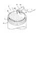
図6に示す吸着パッド5は、円盤状の基台51と吸引保持部材52とからなっている。基台51は適宜の金属材によって構成され、その上面中央部には支持軸部511が突出して形成されており、この支持軸部511が作動アーム53の先端部に装着される。支持軸部511の上端には係止部511aが設けられており、この係止部511aが作動アーム53に形成された係合部531と係合するようになっている。なお、基台51の上面と作動アーム53との間には圧縮コイルばね54が配設され、基台51を下方に向けて付勢している。吸着パッド5を構成する基台51は、下方が開放された円形状の凹部512を備えている。この凹部512に多孔質セラミックによって円盤状に形成された吸引保持部材52が嵌合されている。吸着パッド5を構成する基台51に形成された円形状の凹部512は、支持軸部511に設けられた連通路511bを介して作動アーム53内に配設されたフレキシブルパイプ等の配管54に接続されている。なお、配管54が図示しない吸引手段に接続されている。吸着パッド5を構成する基台51および吸引保持部材52の図6において下面(吸引面)には、多孔質樹脂層を形成する多孔質樹脂シート55が装着されている。この多孔質樹脂シート55は、外周部が基台51の外周面に接着剤によって固着されている。なお、多孔質樹脂シート55は、例えば日東電工株式会社によって製造販売される超高分子量ポリエチレン多孔質シート:サンマップ(商標名)を用いることができる。In this way, when the altered layer forming step is executed along all the division lines 21 formed on the
The
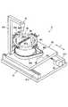
上述した吸着パッド5を用いて実施するウエーハ搬出工程について、図7を参照して説明する。
図7に示すように吸着パッド5の基台51および吸引保持部材52の図7において下面(吸着面)をチャックテーブル41上に保持されている変質層形成工程が実施された半導体ウエーハ2の上面(裏面2b)に接触させる。そして、チャックテーブル41による半導体ウエーハ2の吸引保持を解除するとともに、吸着パッド5の吸引手段を作動する。この結果、作動アーム53に配設された配管54、基台51にもうけられた連通路511bおよび凹部512、吸引保持部材52を介して多孔質樹脂シート55に負圧が作用せしめられる。従って、多孔質樹脂シート55の図7において下面(吸着面)に半導体ウエーハ2の上面(裏面2b)が吸引保持される。そして、図示しない作動機構によって作動アーム53を作動することにより、吸着パッド5に保持された半導体ウエーハ2をチャックテーブル41から搬出する。なお、半導体ウエーハ2の裏面2bを吸引保持する吸着パッド5は、吸着面が多孔質樹脂シート55によって形成されているので、半導体ウエーハ2の裏面2bに微細なクラックが生成されることはない。The wafer carry-out process performed using the
As shown in FIG. 7, the upper surface of the
上述したように半導体ウエーハ2の裏面2bを吸着パッド5に吸引保持してチャックテーブル41から搬出したならば、吸着パッド5に裏面2bが吸引保持されている半導体ウエーハ2の表面2aを保持するとともに半導体ウエーハ2の裏面2bから吸着パッド5を外すウエーハ移し替え工程を実施する。このウエーハ移し替え工程を実施するには図8に示すように上記吸着パッド5と同様の構成をした吸着パッド50を用いる。図8に示す実施形態における吸着パッド50においては、吸着パッド5の構成部材と同一部材には同一符号を付して、その説明は省略する。なお、吸着パッド50においては、吸着パッド5の吸引保持部材52に装着される多孔質樹脂シート55は必要ない。ウエーハ移し替え工程は、図8に示すように吸着パッド5に裏面2bが吸引保持された半導体ウエーハ2の表面2aに貼着されている保護テープ3に吸着パッド50の吸引保持部材52を接触させる。そして、吸着パッド5による半導体ウエーハ2の吸引保持を解除するとともに、吸着パッド50の吸引手段を作動する。この結果、吸引保持部材52に負圧が作用せしめられ、吸引保持部材52に保護テープ3を介して半導体ウエーハ2の表面2a側が吸引保持される。このように、半導体ウエーハ2の表面2aは保護テープ3を介して吸引保持部材52に吸引保持されるので、吸引保持部材52が直接接触しないためデバイスが損傷されることはない。 As described above, when the
次に、吸着パッド50に表面2a側が吸引保持された半導体ウエーハ2の裏面2bを環状のフレームに装着される粘着テープを貼着し、粘着テープを介して半導体ウエーハ2を環状のフレームに支持するウエーハ支持工程を実施する。ウエーハ支持工程は、図9の(a)に示すように半導体ウエーハ2の表面2a側を吸引保持した吸着パッド50を反転し、吸着パッド50に表面2a側が吸引保持された半導体ウエーハ2の裏面2bを、支持台6上に配置されている環状のフレーム7に装着された粘着テープ70の表面に貼着する。そして、吸着パッド50による半導体ウエーハ2の吸引保持を解除する。このようにして、環状のフレーム7に装着された粘着テープ70の表面に半導体ウエーハ2の裏面2bを貼着したならば、図9の(b)に示すように半導体ウエーハ2の表面2aに貼着されている保護テープ3を剥離する。 Next, an adhesive tape attached to an annular frame is attached to the
なお、上述した実施形態におけるウエーハ支持工程は環状のフレーム7に装着された粘着テープ70に半導体ウエーハ2の裏面2bを貼着する例を示したが、環状のフレーム7に粘着テープ70を装着する際に半導体ウエーハ2の裏面2bに粘着テープ70を貼着してもよい。即ち、環状のフレームを保持する保持手段を設け、該保持手段によって環状のフレームを保持する。そして、ウエーハを環状のフレーム内に裏面を上側にしてセットし、粘着テープを環状のフレームおよびウエーハ裏面に貼着した後、粘着テープを環状のフレームに沿って切断する。 In addition, although the wafer support process in the above-described embodiment shows an example in which the
上述したウエーハ支持工程を実施したならば、環状のフレーム7に粘着テープ70を介して支持された半導体ウエーハ2に外力を作用せしめることにより変質層210が形成された分割予定ライン21に沿って半導体ウエーハ2を破断するウエーハ破断工程を実施する。このウエーハ破断工程は、図10に示す分割装置8を用いて実施する。
図10に示す分割装置8は、基台81と、該基台81上に矢印Yで示す方向に移動可能に配設された移動テーブル82を具備している。基台81は矩形状に形成され、その両側部上面には矢印Yで示す方向に2本の案内レール811、812が互いに平行に配設されている。この2本の案内レール811、812上に移動テーブル82が移動可能に配設されている。移動テーブル82は、移動手段83によって矢印Yで示す方向に移動せしめられる。移動テーブル82上には、上記環状のフレーム7を保持するフレーム保持手段84が配設されている。フレーム保持手段84は、円筒状の本体841と、該本体841の上端に設けられた環状のフレーム保持部材842と、該フレーム保持部材842の外周に配設された固定手段としての複数のクランプ843とからなっている。このように構成されたフレーム保持手段84は、フレーム保持部材842上に載置された環状のフレーム7をクランプ843によって固定する。また、図10に示す分割装置8は、上記フレーム保持手段84を回動せしめる回動手段85を具備している。この回動手段85は、上記移動テーブル82に配設されたパルスモータ851と、該パルスモータ851の回転軸に装着されたプーリ852と、該プーリ852と円筒状の本体841に捲回された無端ベルト853とからなっている。このように構成された回動手段85は、パルスモータ851を駆動することにより、プーリ852および無端ベルト853を介してフレーム保持手段84を回動せしめる。If the wafer support process described above is performed, the semiconductor is moved along the
The
図10に示す分割装置8は、上記環状のフレーム保持部材842に保持された環状のフレーム7に粘着テープ70を介して支持されている半導体ウエーハ2に分割予定ラインと直交する方向に引張力を作用せしめる張力付与手段86を具備している。張力付与手段86は、環状のフレーム保持部材84の本体841内に配置されている。この張力付与手段86は、矢印Y方向と直交する方向に長い長方形の保持面を備えた第1の吸引保持部材861と第2の吸引保持部材862を備えている。第1の吸引保持部材861には複数の吸引孔861aが形成されており、第2の吸引保持部材862には複数の吸引孔862aが形成されている。複数の吸引孔861aおよび862aは、図示しない吸引手段に連通されている。また、第1の吸引保持部材861と第2の吸引保持部材862は、図示しない移動手段によって矢印Y方向にそれぞれ移動せしめられるようになっている。 The
図10に示す分割装置8は、上記環状のフレーム保持部材842に保持された環状のフレーム7に粘着テープ70を介して支持されている半導体ウエーハ2の分割予定ラインを検出するための検出手段87を具備している。検出手段87は、基台81に配設されたL字状の支持柱871に取り付けられている。この検出手段87は、光学系および撮像素子(CCD)等で構成されており、上記張力付与手段86の上方位置に配置されている。このように構成された検出手段87は、上記環状のフレーム保持部材842に保持された環状のフレーム7に粘着テープ70を介して支持されている半導体ウエーハ2の分割予定ラインを撮像し、これを電気信号に変換して図示しない制御手段に送る。 The
上述した分割装置8を用いて実施するウエーハ破断工程について、図10乃至図11を参照して説明する。
上述した変質層形成工程が実施された半導体ウエーハ2を粘着テープ70を介して支持する環状のフレーム7を、図11の(a)に示すようにフレーム保持部材842上に載置し、クランプ843によってフレーム保持部材842に固定する。次に、移動手段83を作動して移動テーブル82を矢印Yで示す方向(図10参照)に移動し、図11の(a)に示すように半導体ウエーハ2の所定方向に形成された1本の分割予定ライン21(図示の実施形態においては最左端の分割予定ライン)が張力付与手段86を構成する第1の吸引保持部材861の保持面と第2の吸引保持部材862の保持面との間に位置付ける。このとき、検出手段87によって分割予定ライン21を撮像し、第1の吸引保持部材861の保持面と第2の吸引保持部材862の保持面との位置合わせを行う。このようにして、1本の分割予定ライン21が第1の吸引保持部材861の保持面と第2の吸引保持部材862の保持面との間に位置付けられたならば、図示しない吸引手段を作動し吸引孔861aおよび862aに負圧を作用せしめることにより、第1の吸引保持部材861の保持面と第2の吸引保持部材862の保持面上に粘着テープ70を介して半導体ウエーハ2を吸引保持する(保持工程)。A wafer breaking process performed using the above-described
An
上述した保持工程を実施したならば、張力付与手段86を構成する図示しない移動手段を作動し、第1の吸引保持部材861と第2の吸引保持部材862を図11の(b)に示すように互いに離反する方向に移動せしめる。この結果、第1の吸引保持部材861の保持面と第2の吸引保持部材862の保持面との間に位置付けられた分割予定ライン21には、分割予定ライン21と直交する方向に引張力が作用して、半導体ウエーハ2は分割予定ライン21に沿って破断される。このウエーハ破断工程を実施することにより、粘着テープ70は僅かに伸びる。このウエーハ破断工程においては、半導体ウエーハ2は分割予定ライン21に沿って変質層210が形成され強度が低下せしめられているので、第1の吸引保持部材861と第2の吸引保持部材862を互いに離反する方向に0.5mm程度移動することにより半導体ウエーハ2を分割予定ライン21に沿って破断することができる。 When the holding step described above is performed, the moving means (not shown) constituting the
上述したように所定方向に形成された1本の分割予定ライン21に沿って破断するウエーハ破断工程を実施したならば、上述した第1の吸引保持部材861および第2の吸引保持部材862による半導体ウエーハ2の吸引保持を解除する。次に、移動手段83を作動して移動テーブル82を矢印Yで示す方向(図10参照)に分割予定ライン21の間隔に相当する分だけ移動し、上記ウエーハ破断工程を実施した分割予定ライン21の隣の分割予定ライン21が張力付与手段86を構成する第1の吸引保持部材861の保持面と第2の吸引保持部材862の保持面との間に位置付ける。そして、上記保持工程およびウエーハ破断工程を実施する。 As described above, if the wafer breaking step for breaking along one division planned
以上のようにして、所定方向に形成された全ての分割予定ライン21に対して上記保持工程および分割工程を実施したならば、回動手段85を作動してフレーム保持手段84を90度回動せしめる。この結果、フレーム保持手段84のフレーム保持部材862に保持された半導体ウエーハ2も90度回動することになり、所定方向に形成され上記ウエーハ破断工程が実施された分割予定ライン21と直交する方向に形成された分割予定ライン21が第1の吸引保持部材861の保持面と第2の吸引保持部材862の保持面と平行な状態に位置付けられる。次に、上記分割工程が実施された分割予定ライン21と直交する方向に形成された全ての分割予定ライン21に対して上述し保持工程およびウエーハ破断工程を実施することにより、半導体ウエーハ2は分割予定ライン21に沿って個々のデバイス(チップ)に分割される。このようにして個々に分割されたデバイス(チップ)は、上記ウエーハ搬出工程において上述したように裏面に微細なクラックが生成されないので、抗折強度が低下することはない。 As described above, when the holding step and the dividing step are performed on all the division lines 21 formed in the predetermined direction, the
なお、ウエーハ破断工程は上述した破断方法の外に、次のような分割方法を用いることができる。
即ち、粘着テープ50に貼着された半導体ウエーハ2(分割予定ライン21に沿って変質層210が形成されている)を柔軟なゴムシート上に載置し、その上面をローラーによって押圧することによって、半導体ウエーハ2を変質層210が形成され強度が低下した分割予定ライン21に沿って割断する方法を用いることができる。また、変質層が形成され強度が低下したス分割予定ライン21に沿って例えば周波数が28kHz程度の縦波(疎密波)からなる超音波を作用せしめる方法や、変質層210が形成され強度が低下した分割予定ライン21に沿って押圧部材を作用せしめる方法、或いは変質層210が形成され強度が低下した分割予定ライン21に沿ってレーザー光線を照射してヒートショックを与える方法等を用いることができる。In addition to the breaking method described above, the following breaking method can be used for the wafer breaking process.
That is, by placing the semiconductor wafer 2 (having the altered
上述した実施形態においてはIC、LSI等のデバイスが形成された半導体ウエーハを個々のデバイス(チップ)に分割する例を示したが、本発明によるウエーハの分割方法は石英ガラスのようにデバイスが形成されていないウエーハの分割にも適用できる。 In the embodiment described above, an example is shown in which a semiconductor wafer on which devices such as IC and LSI are formed is divided into individual devices (chips). However, the wafer dividing method according to the present invention forms a device like quartz glass. It can also be applied to undivided wafer divisions.
2:半導体ウエーハ
21:分割予定ライン
22:デバイス
210:変質層
3:保護テープ
4:レーザー加工装置
41:レーザー加工装置のチャックテーブル
42:レーザー光線照射手段
43:撮像手段
5:吸着パッド
50:吸着パッド
51:円盤状の基台
52:吸引保持部材
53:作動アーム
55:多孔質樹脂シート
7:環状のフレーム
70:粘着テープ
8:分割装置
81:フレーム保持手段
82:テープ拡張手段
83:支持手段2: Semiconductor wafer 21: Planned division line 22: Device
210: Altered layer 3: Protection tape 4: Laser processing device 41: Chuck table of laser processing device 42: Laser beam irradiation means 43: Imaging means 5: Adsorption pad 50: Adsorption pad 51: Disc-shaped base 52: Suction holding member 53: Actuating arm 55: Porous resin sheet 7: Ring frame 70: Adhesive tape 8: Dividing device 81: Frame holding means 82: Tape expanding means 83: Support means
Claims (2)
Translated fromJapanese該ウエーハの表面に保護テープを貼着する保護テープ貼着工程と、
レーザー加工装置の被加工物を保持するチャックテーブルにウエーハの保護テープ側を保持するウエーハ保持工程と、
該チャックテーブルに保持されたウエーハに対して透過性を有する波長のレーザー光線をウエーハの裏面側から該分割予定ラインに沿って照射し、ウエーハの内部に該分割予定ラインに沿って変質層を形成する変質層形成工程と、
該変質層形成工程を実施した後に、吸着面に多孔質樹脂層を有する吸着パッドによって該チャックテーブルに保持されているウエーハの裏面を吸引保持し、該チャックテーブルからウエーハを搬出するウエーハ搬出工程と、
該吸着パッドに裏面が吸引保持されているウエーハの表面を保持するとともにウエーハの裏面から該吸着パッドを外し、ウエーハの裏面に環状のフレームに装着される粘着テープを貼着し、該粘着テープを介してウエーハを該環状のフレームに支持するウエーハ支持工程と、
該環状のフレームに該粘着テープを介して支持されたウエーハに外力を作用せしめることにより該変質層が形成された該分割予定ラインに沿ってウエーハを破断するウエーハ破断工程と、を含む、
ことを特徴とするウエーハの分割方法。A wafer dividing method for dividing a wafer having a line to be divided formed on a surface along the line to be divided,
A protective tape attaching step of attaching a protective tape to the surface of the wafer;
A wafer holding step for holding the protective tape side of the wafer on a chuck table for holding a workpiece of the laser processing apparatus;
A laser beam having a wavelength that is transparent to the wafer held on the chuck table is irradiated from the back side of the wafer along the division line to form a deteriorated layer along the division line inside the wafer. An altered layer forming step;
A wafer unloading step of sucking and holding the back surface of the wafer held on the chuck table by a suction pad having a porous resin layer on the suction surface after carrying out the deteriorated layer forming step, and unloading the wafer from the chuck table; ,
While holding the front surface of the wafer whose back surface is sucked and held on the suction pad, the suction pad is removed from the back surface of the wafer, and an adhesive tape attached to an annular frame is attached to the back surface of the wafer. A wafer support step for supporting the wafer on the annular frame via,
A wafer breaking step of breaking the wafer along the division line in which the altered layer is formed by applying an external force to the wafer supported by the annular frame via the adhesive tape,
A wafer dividing method characterized by the above.
Priority Applications (2)
| Application Number | Priority Date | Filing Date | Title |
|---|---|---|---|
| JP2006061088AJP2007242787A (en) | 2006-03-07 | 2006-03-07 | Wafer division method |
| CN2007100856587ACN101032843B (en) | 2006-03-07 | 2007-03-06 | Wafer division method |
Applications Claiming Priority (1)
| Application Number | Priority Date | Filing Date | Title |
|---|---|---|---|
| JP2006061088AJP2007242787A (en) | 2006-03-07 | 2006-03-07 | Wafer division method |
Publications (1)
| Publication Number | Publication Date |
|---|---|
| JP2007242787Atrue JP2007242787A (en) | 2007-09-20 |
Family
ID=38588053
Family Applications (1)
| Application Number | Title | Priority Date | Filing Date |
|---|---|---|---|
| JP2006061088APendingJP2007242787A (en) | 2006-03-07 | 2006-03-07 | Wafer division method |
Country Status (2)
| Country | Link |
|---|---|
| JP (1) | JP2007242787A (en) |
| CN (1) | CN101032843B (en) |
Cited By (5)
| Publication number | Priority date | Publication date | Assignee | Title |
|---|---|---|---|---|
| JP2014011381A (en)* | 2012-07-02 | 2014-01-20 | Disco Abrasive Syst Ltd | Wafer processing method |
| JP2014013807A (en)* | 2012-07-04 | 2014-01-23 | Disco Abrasive Syst Ltd | Wafer processing method |
| CN107316833A (en)* | 2016-04-27 | 2017-11-03 | 株式会社迪思科 | The processing method of chip |
| JP2019009191A (en)* | 2017-06-21 | 2019-01-17 | 株式会社ディスコ | Processing method of wafer |
| CN112885746A (en)* | 2021-01-20 | 2021-06-01 | 中国科学院微电子研究所 | Lobe of a leaf device |
Families Citing this family (8)
| Publication number | Priority date | Publication date | Assignee | Title |
|---|---|---|---|---|
| EP2209586A1 (en)* | 2007-11-07 | 2010-07-28 | CeramTec AG | Method for the laser ablation of brittle components |
| JP2009272503A (en)* | 2008-05-09 | 2009-11-19 | Disco Abrasive Syst Ltd | Breaking device and breaking method for filmy adhesive |
| JP2010272639A (en)* | 2009-05-20 | 2010-12-02 | Disco Abrasive Syst Ltd | Grinding equipment |
| JP2016102048A (en)* | 2014-11-13 | 2016-06-02 | 三星ダイヤモンド工業株式会社 | Scribe method and scribe device |
| CN106583757A (en)* | 2016-11-30 | 2017-04-26 | 中国人民解放军国防科学技术大学 | Processing device and processing method for high-accuracy ultra-thin metal foils |
| US20190363020A1 (en)* | 2018-05-24 | 2019-11-28 | Semiconductor Components Industries, Llc | Die singulation systems and methods |
| JP7140576B2 (en)* | 2018-07-12 | 2022-09-21 | 株式会社ディスコ | Wafer division method |
| JP7218056B2 (en)* | 2019-02-20 | 2023-02-06 | 株式会社ディスコ | Method for manufacturing at least one of chip and frame |
Citations (4)
| Publication number | Priority date | Publication date | Assignee | Title |
|---|---|---|---|---|
| JPH11243135A (en)* | 1998-02-26 | 1999-09-07 | Kyocera Corp | Vacuum suction cup |
| JP2000021952A (en)* | 1998-04-27 | 2000-01-21 | Tokyo Seimitsu Co Ltd | Flattening device for wafer |
| JP2005150177A (en)* | 2003-11-12 | 2005-06-09 | Nitto Denko Corp | Adhesive tape application method and adhesive tape application device on backside of semiconductor wafer |
| JP2005203541A (en)* | 2004-01-15 | 2005-07-28 | Disco Abrasive Syst Ltd | Wafer laser processing method |
Family Cites Families (10)
| Publication number | Priority date | Publication date | Assignee | Title |
|---|---|---|---|---|
| JP3620554B2 (en)* | 1996-03-25 | 2005-02-16 | 信越半導体株式会社 | Semiconductor wafer manufacturing method |
| JP3810714B2 (en)* | 2002-07-29 | 2006-08-16 | エスペック株式会社 | Thin layer substrate manufacturing method, thin layer substrate transfer device, and thin layer substrate transfer suction pad |
| JP2004153193A (en)* | 2002-11-01 | 2004-05-27 | Disco Abrasive Syst Ltd | Semiconductor wafer processing method |
| JP3917528B2 (en)* | 2003-01-07 | 2007-05-23 | エスペック株式会社 | Suction pad |
| JP4554901B2 (en)* | 2003-08-12 | 2010-09-29 | 株式会社ディスコ | Wafer processing method |
| JP4590174B2 (en)* | 2003-09-11 | 2010-12-01 | 株式会社ディスコ | Wafer processing method |
| JP4592270B2 (en)* | 2003-10-06 | 2010-12-01 | 日東電工株式会社 | Method for peeling semiconductor wafer from support and apparatus using the same |
| JP2005129607A (en)* | 2003-10-22 | 2005-05-19 | Disco Abrasive Syst Ltd | Wafer division method |
| CN100428418C (en)* | 2004-02-09 | 2008-10-22 | 株式会社迪斯科 | Wafer Separation Method |
| JP4471747B2 (en)* | 2004-06-24 | 2010-06-02 | アピックヤマダ株式会社 | Semiconductor device manufacturing equipment |
- 2006
- 2006-03-07JPJP2006061088Apatent/JP2007242787A/enactivePending
- 2007
- 2007-03-06CNCN2007100856587Apatent/CN101032843B/enactiveActive
Patent Citations (4)
| Publication number | Priority date | Publication date | Assignee | Title |
|---|---|---|---|---|
| JPH11243135A (en)* | 1998-02-26 | 1999-09-07 | Kyocera Corp | Vacuum suction cup |
| JP2000021952A (en)* | 1998-04-27 | 2000-01-21 | Tokyo Seimitsu Co Ltd | Flattening device for wafer |
| JP2005150177A (en)* | 2003-11-12 | 2005-06-09 | Nitto Denko Corp | Adhesive tape application method and adhesive tape application device on backside of semiconductor wafer |
| JP2005203541A (en)* | 2004-01-15 | 2005-07-28 | Disco Abrasive Syst Ltd | Wafer laser processing method |
Cited By (5)
| Publication number | Priority date | Publication date | Assignee | Title |
|---|---|---|---|---|
| JP2014011381A (en)* | 2012-07-02 | 2014-01-20 | Disco Abrasive Syst Ltd | Wafer processing method |
| JP2014013807A (en)* | 2012-07-04 | 2014-01-23 | Disco Abrasive Syst Ltd | Wafer processing method |
| CN107316833A (en)* | 2016-04-27 | 2017-11-03 | 株式会社迪思科 | The processing method of chip |
| JP2019009191A (en)* | 2017-06-21 | 2019-01-17 | 株式会社ディスコ | Processing method of wafer |
| CN112885746A (en)* | 2021-01-20 | 2021-06-01 | 中国科学院微电子研究所 | Lobe of a leaf device |
Also Published As
| Publication number | Publication date |
|---|---|
| CN101032843A (en) | 2007-09-12 |
| CN101032843B (en) | 2011-12-21 |
Similar Documents
| Publication | Publication Date | Title |
|---|---|---|
| JP2007242787A (en) | Wafer division method | |
| JP5307384B2 (en) | Wafer division method | |
| JP4769560B2 (en) | Wafer division method | |
| JP5307612B2 (en) | Processing method of optical device wafer | |
| JP4767711B2 (en) | Wafer division method | |
| JP5595716B2 (en) | Processing method of optical device wafer | |
| JP2008294191A (en) | Wafer division method | |
| JP4777761B2 (en) | Wafer division method | |
| KR102102485B1 (en) | Wafer machining method | |
| JP2005203541A (en) | Wafer laser processing method | |
| JP2011091293A (en) | Method for processing wafer | |
| JP2009200140A (en) | Method of manufacturing semiconductor chip | |
| JP2006229021A (en) | Wafer division method | |
| JP2005332841A (en) | Wafer division method | |
| JP4447392B2 (en) | Wafer dividing method and dividing apparatus | |
| JP2006108273A (en) | Wafer dividing method and dividing apparatus | |
| JP5623807B2 (en) | Method for dividing optical device wafer | |
| JP2011151070A (en) | Processing method for wafer | |
| JP4833657B2 (en) | Wafer division method | |
| KR20130054912A (en) | Optical device layer transferring apparatus and laser machining apparatus | |
| JP2006202933A (en) | Wafer division method | |
| JP2006128211A (en) | Wafer divider | |
| JP2015023135A (en) | Wafer processing method | |
| JP2005251986A (en) | Wafer separation detection method and separation detection apparatus | |
| JP2019034391A (en) | Processing method |
Legal Events
| Date | Code | Title | Description |
|---|---|---|---|
| A621 | Written request for application examination | Effective date:20090203 Free format text:JAPANESE INTERMEDIATE CODE: A621 | |
| A977 | Report on retrieval | Free format text:JAPANESE INTERMEDIATE CODE: A971007 Effective date:20110311 | |
| A131 | Notification of reasons for refusal | Free format text:JAPANESE INTERMEDIATE CODE: A131 Effective date:20110607 | |
| A02 | Decision of refusal | Free format text:JAPANESE INTERMEDIATE CODE: A02 Effective date:20111018 |