JP2007240698A - Current drive circuit - Google Patents
Current drive circuitDownload PDFInfo
- Publication number
- JP2007240698A JP2007240698AJP2006060621AJP2006060621AJP2007240698AJP 2007240698 AJP2007240698 AJP 2007240698AJP 2006060621 AJP2006060621 AJP 2006060621AJP 2006060621 AJP2006060621 AJP 2006060621AJP 2007240698 AJP2007240698 AJP 2007240698A
- Authority
- JP
- Japan
- Prior art keywords
- current
- node
- display
- write control
- capacitor
- Prior art date
- Legal status (The legal status is an assumption and is not a legal conclusion. Google has not performed a legal analysis and makes no representation as to the accuracy of the status listed.)
- Pending
Links
- 239000003990capacitorSubstances0.000claimsabstractdescription31
- 238000005513bias potentialMethods0.000claimsdescription4
- 238000006243chemical reactionMethods0.000abstractdescription8
- 230000004044responseEffects0.000abstractdescription8
- 238000010586diagramMethods0.000description12
- 101100367244Arabidopsis thaliana SWA1 geneProteins0.000description11
- 230000008901benefitEffects0.000description3
- 238000007599dischargingMethods0.000description3
- 230000008859changeEffects0.000description2
- 230000000694effectsEffects0.000description1
- 230000014759maintenance of locationEffects0.000description1
- 230000004048modificationEffects0.000description1
- 238000012986modificationMethods0.000description1
- 230000009466transformationEffects0.000description1
Images


Classifications
- G—PHYSICS
- G09—EDUCATION; CRYPTOGRAPHY; DISPLAY; ADVERTISING; SEALS
- G09G—ARRANGEMENTS OR CIRCUITS FOR CONTROL OF INDICATING DEVICES USING STATIC MEANS TO PRESENT VARIABLE INFORMATION
- G09G3/00—Control arrangements or circuits, of interest only in connection with visual indicators other than cathode-ray tubes
- G09G3/20—Control arrangements or circuits, of interest only in connection with visual indicators other than cathode-ray tubes for presentation of an assembly of a number of characters, e.g. a page, by composing the assembly by combination of individual elements arranged in a matrix no fixed position being assigned to or needed to be assigned to the individual characters or partial characters
- G09G3/22—Control arrangements or circuits, of interest only in connection with visual indicators other than cathode-ray tubes for presentation of an assembly of a number of characters, e.g. a page, by composing the assembly by combination of individual elements arranged in a matrix no fixed position being assigned to or needed to be assigned to the individual characters or partial characters using controlled light sources
- G09G3/30—Control arrangements or circuits, of interest only in connection with visual indicators other than cathode-ray tubes for presentation of an assembly of a number of characters, e.g. a page, by composing the assembly by combination of individual elements arranged in a matrix no fixed position being assigned to or needed to be assigned to the individual characters or partial characters using controlled light sources using electroluminescent panels
- G09G3/32—Control arrangements or circuits, of interest only in connection with visual indicators other than cathode-ray tubes for presentation of an assembly of a number of characters, e.g. a page, by composing the assembly by combination of individual elements arranged in a matrix no fixed position being assigned to or needed to be assigned to the individual characters or partial characters using controlled light sources using electroluminescent panels semiconductive, e.g. using light-emitting diodes [LED]
- G09G3/3208—Control arrangements or circuits, of interest only in connection with visual indicators other than cathode-ray tubes for presentation of an assembly of a number of characters, e.g. a page, by composing the assembly by combination of individual elements arranged in a matrix no fixed position being assigned to or needed to be assigned to the individual characters or partial characters using controlled light sources using electroluminescent panels semiconductive, e.g. using light-emitting diodes [LED] organic, e.g. using organic light-emitting diodes [OLED]
- G09G3/3225—Control arrangements or circuits, of interest only in connection with visual indicators other than cathode-ray tubes for presentation of an assembly of a number of characters, e.g. a page, by composing the assembly by combination of individual elements arranged in a matrix no fixed position being assigned to or needed to be assigned to the individual characters or partial characters using controlled light sources using electroluminescent panels semiconductive, e.g. using light-emitting diodes [LED] organic, e.g. using organic light-emitting diodes [OLED] using an active matrix
- G09G3/3233—Control arrangements or circuits, of interest only in connection with visual indicators other than cathode-ray tubes for presentation of an assembly of a number of characters, e.g. a page, by composing the assembly by combination of individual elements arranged in a matrix no fixed position being assigned to or needed to be assigned to the individual characters or partial characters using controlled light sources using electroluminescent panels semiconductive, e.g. using light-emitting diodes [LED] organic, e.g. using organic light-emitting diodes [OLED] using an active matrix with pixel circuitry controlling the current through the light-emitting element
- G—PHYSICS
- G09—EDUCATION; CRYPTOGRAPHY; DISPLAY; ADVERTISING; SEALS
- G09G—ARRANGEMENTS OR CIRCUITS FOR CONTROL OF INDICATING DEVICES USING STATIC MEANS TO PRESENT VARIABLE INFORMATION
- G09G3/00—Control arrangements or circuits, of interest only in connection with visual indicators other than cathode-ray tubes
- G09G3/20—Control arrangements or circuits, of interest only in connection with visual indicators other than cathode-ray tubes for presentation of an assembly of a number of characters, e.g. a page, by composing the assembly by combination of individual elements arranged in a matrix no fixed position being assigned to or needed to be assigned to the individual characters or partial characters
- G09G3/22—Control arrangements or circuits, of interest only in connection with visual indicators other than cathode-ray tubes for presentation of an assembly of a number of characters, e.g. a page, by composing the assembly by combination of individual elements arranged in a matrix no fixed position being assigned to or needed to be assigned to the individual characters or partial characters using controlled light sources
- G09G3/30—Control arrangements or circuits, of interest only in connection with visual indicators other than cathode-ray tubes for presentation of an assembly of a number of characters, e.g. a page, by composing the assembly by combination of individual elements arranged in a matrix no fixed position being assigned to or needed to be assigned to the individual characters or partial characters using controlled light sources using electroluminescent panels
- G09G3/32—Control arrangements or circuits, of interest only in connection with visual indicators other than cathode-ray tubes for presentation of an assembly of a number of characters, e.g. a page, by composing the assembly by combination of individual elements arranged in a matrix no fixed position being assigned to or needed to be assigned to the individual characters or partial characters using controlled light sources using electroluminescent panels semiconductive, e.g. using light-emitting diodes [LED]
- G09G3/3208—Control arrangements or circuits, of interest only in connection with visual indicators other than cathode-ray tubes for presentation of an assembly of a number of characters, e.g. a page, by composing the assembly by combination of individual elements arranged in a matrix no fixed position being assigned to or needed to be assigned to the individual characters or partial characters using controlled light sources using electroluminescent panels semiconductive, e.g. using light-emitting diodes [LED] organic, e.g. using organic light-emitting diodes [OLED]
- G09G3/3275—Details of drivers for data electrodes
- G09G3/3283—Details of drivers for data electrodes in which the data driver supplies a variable data current for setting the current through, or the voltage across, the light-emitting elements
- G—PHYSICS
- G09—EDUCATION; CRYPTOGRAPHY; DISPLAY; ADVERTISING; SEALS
- G09G—ARRANGEMENTS OR CIRCUITS FOR CONTROL OF INDICATING DEVICES USING STATIC MEANS TO PRESENT VARIABLE INFORMATION
- G09G2310/00—Command of the display device
- G09G2310/02—Addressing, scanning or driving the display screen or processing steps related thereto
- G09G2310/0264—Details of driving circuits
- G09G2310/027—Details of drivers for data electrodes, the drivers handling digital grey scale data, e.g. use of D/A converters
Landscapes
- Engineering & Computer Science (AREA)
- Physics & Mathematics (AREA)
- Computer Hardware Design (AREA)
- General Physics & Mathematics (AREA)
- Theoretical Computer Science (AREA)
- Control Of Indicators Other Than Cathode Ray Tubes (AREA)
- Control Of El Displays (AREA)
Abstract
Description
Translated fromJapanese本発明は、表示装置等に駆動用の電流を供給する電流駆動回路に関するものである。 The present invention relates to a current driving circuit for supplying a driving current to a display device or the like.
図2は、従来の電流駆動回路の構成図である。
この電流駆動回路は、電流駆動型の表示装置1に駆動用の電流を供給するもので、基準電流生成部10、ディジタル・アナログ変換部(以下、「DA変換部」という)20、複数の電流ラッチ部301〜30n、及びタイミング制御部40を備えている。FIG. 2 is a configuration diagram of a conventional current driving circuit.
This current drive circuit supplies a drive current to the current drive
基準電流生成部10は、基準電圧Vrefと基準抵抗Rrefで規定される基準電流Irefを生成し、この基準電流Irefに対応するバイアス電圧VBを出力するもので、電源電位VDDとノードN1の間に接続されたPチャネルMOSトランジスタ(以下、「PMOS」という)11、ノードN1と接地電位GNDの間に接続された抵抗12、及び演算増幅器(OP)13で構成されている。演算増幅器13の第1の入力側には基準電圧Vrefが与えられ、第2の入力側はノードN1に接続されている。また、演算増幅器13の出力側はPMOS11のゲートに接続され、この演算増幅器13の出力側から、バイアス電圧VBが出力されるようになっている。 The reference
DA変換部20は、例えば8ビットの表示データDinの値に応じた大きさの表示電流SNKを出力するもので、ドレインがノードN2に共通接続され、ゲートにはバイアス電圧VBが共通に与えられる8個のPMOS210〜207と、これらの各PMOS210〜207のソースと電源電位VDDの間に接続されたスイッチ220〜227で構成されている。スイッチ220〜227は、表示データDinを構成する8ビットの信号b0〜b7によって、それぞれオン・オフ制御されるようになっている。また、PMOS210〜207のディメンジョンは、対応するスイッチ220〜227がオンとなったときに、それぞれ基準電流Irefの1,2,4,…,128倍に重み付けした電流が流れるように設定されている。これにより、表示データDinの値Di(但し、i=1〜n)に応じて、ノードN2からDi×Irefの大きさの表示電流SNKが出力されるようになっている。The DA converter 20 outputs a display current SNK having a magnitude corresponding to, for example, the value of 8-bit display data Din, the drain is commonly connected to the node N2, and the bias voltage VB is commonly applied to the gates. and eight
電流ラッチ部301〜30nは、いずれも同様の構成で、例えば電流ラッチ部301に示すように、表示電流SNKが出力されるDA変換部20のノードN2と、この電流ラッチ部301内のノードN3の間に接続されたスイッチ31、及びノードN3とノードN4の間に接続されたスイッチ32を有している。これらのスイッチ31,32は、タイミング制御部40から与えられる書込制御信号W1によってオン・オフ制御されるものである。更に、電流ラッチ部30は、ノードN3にドレインとゲートが接続され、ソースが接地電位GNDに接続されたNチャネルMOSトランジスタ(以下、「NMOS」という)33、ノードN4と接地電位GNDの間に接続されたキャパシタ34、及びゲートとソースがそれぞれノードN4と接地電位GNDに接続されたNMOS35を有している。そして、NMOS35のドレインが表示装置1の対応する表示ラインに接続され、このNMOS35に流入する駆動電流OUT1によって表示装置1を駆動するようになっている。
タイミング制御部40は、DA変換部20に与えられる表示データDinに同期して、電流ラッチ部301〜30nに対する書込制御信号W1〜Wnを、順番に周期的に出力するものである。The
次に動作を説明する。
基準電流生成部10において、演算増幅器13の出力側から第1と第2の入力側の電圧の差に応じた信号が出力され、PMOS11の導通状態が制御される。PMOS11のドレイン(即ち、ノードN1)の電圧は、演算増幅器13の入力側にフィードバックされるので、最終的にノードN1の電圧は基準電圧Vrefとなる。従って、PMOS11と抵抗12に流れる電流は基準電流Irefとなり、この基準電流Irefに対応するPMOS11のバイアス電圧VBが、DA変換部20に与えられる。Next, the operation will be described.
In the reference
DA変換部20では、与えられる表示データDinの値(ここでは、D1とする)に応じてスイッチ220〜227が制御され、オンとなったスイッチ220〜227に対応するPMOS210〜217にそれぞれ重み付けされた電流が流れる。これにより、DA変換部20のノードN2から、表示データDinの値D1に対応して、D1×Irefの大きさの表示電流SNKが出力される。The DA converter 20 (herein, a D1) value of the display data supplied Din switch22 0-227 depending on is controlled, corresponding to the switch22 0-227 turned on
タイミング制御部40では、現在与えられている表示データDinに対応する1つの電流ラッチ部(ここでは、301)に書込制御信号W1を出力する。なお、他の電流ラッチ部302〜30nに対する書込制御信号W2〜Wnは出力されない。これにより、対応する電流ラッチ部301のスイッチ31,32がオンとなり、DA変換部20から出力された表示電流SNKがNMOS33に流れる。これに応じて、NMOS35にも表示電流SNKと同じD1×Irefの大きさの駆動電流OUT1が流れる。また、キャパシタ34は、この時のNMOS35のゲート電圧に充電される。The
その後、表示データDinが、次の電流ラッチ部302に対応する値D2に変化すると、タイミング制御部40から出力されていた書込制御信号W1は停止し、代わって電流ラッチ部302に対する書込制御信号W2が出力される。これにより、電流ラッチ部302のNMOS35には、次の表示データDinに応じてD2×Irefの大きさの駆動電流OUT2が流れる。Thereafter, the display data Din is, when changes to a value D2 corresponding to the next current latching portion 302, the write control signal W1 which has been outputted from the
一方、電流ラッチ部301では、書込制御信号W1の停止によりスイッチ31,32がオフとなる。これにより、NMOS33に流れる電流はなくなるが、キャパシタ34はD1×Irefの大きさの電流に対応するゲート電圧に充電されているので、NMOS35にはD1×Irefの大きさの駆動電流OUT1が流れ続ける。On the other hand, the current latch section 301,
同様の動作により、各電流ラッチ部301〜30nのNMOS35には、それぞれ表示データDinの値D1〜Dnに対応する駆動電流OUT1〜OUTnが流れ続ける。By the similar operation, the drive currents OUT1 to OUTn corresponding to the values D1 to Dn of the display data Din continue to flow through the
しかしながら、前記電流駆動回路では、次のような課題があった。
電流ラッチ部301〜30nに流れる駆動電流OUT1〜OUTnは、表示データDinの値に従って変化する。駆動電流OUT1〜OUTnの大きさは、書込制御信号W1〜Wnが与えられたときに、各電流ラッチ部301〜30nのキャパシタ34に充電される電圧によって決定される。従って、キャパシタ34の電圧は、書込制御信号W1〜Wnが与えられている間に新たな駆動電流OUT1〜OUTnに対応する電圧に変化する必要がある。しかし、図2中の電流ラッチ部301〜30nには、キャパシタ34の電荷を有効に放電するための回路が存在しない。従って、例えば次の表示データDinに対する駆動電流が0となった場合、キャパシタ34の電荷を完全に放電することができず、ノードN4の電圧は、NMOS33の閾値電圧に保持される。このため、駆動電流OUT1〜OUTnの小さい領域では、電流精度が悪化する。However, the current driving circuit has the following problems.
The drive currents OUT1 to OUTn flowing through the current latch units 301 to 30n change according to the value of the display data Din. The magnitudes of the drive currents OUT1 to OUTn are determined by the voltages charged in the
また、電流書き込みに必要な時間は、書き込む表示電流SNKの大きさに逆比例するため、表示電流SNKが微小な領域で長くなって収束に時間がかかる。このため、表示速度を高速化することが困難であった。 In addition, the time required for current writing is inversely proportional to the magnitude of the display current SNK to be written, so that the display current SNK becomes longer in a minute region and takes time to converge. For this reason, it has been difficult to increase the display speed.
本発明は、駆動電流精度が高く、かつ応答速度が速い電流駆動回路を提供すること目的としている。 An object of the present invention is to provide a current drive circuit with high drive current accuracy and quick response speed.
本発明は、入力データの値に応じて表示電流生成手段から順次出力される表示電流を、書込制御信号に従って保持して駆動電流として出力する電流駆動回路を、次のように構成している。 According to the present invention, a current driving circuit that holds display currents sequentially output from display current generating means according to input data values according to a write control signal and outputs them as drive current is configured as follows. .
即ち、この電流駆動回路は、表示電流が出力される第1のノードと第2のノードとの間を第1の書込制御信号に従ってオン・オフする第1のスイッチと、第2のノードにドレインとゲートが接続され、共通電位にソースが接続された第1のトランジスタと、第2のノードと第3のノードの間を第2の書込制御信号に従ってオン・オフする第2のスイッチと、第3のノードと共通電位の間に接続されてこの第3のノードの電位を保持するキャパシタと、第3のノードと共通電位の間に接続され、第1及び第2の書込制御信号に先立って与えられるリセット信号によってオン状態となる第2のトランジスタと、第3のノードと共通電位にゲートとソースがそれぞれ接続され、ドレインから駆動電流を出力する第3のトランジスタを備えたことを特徴としている。 That is, the current driving circuit includes a first switch that turns on and off according to a first write control signal between a first node and a second node that output a display current, and a second node. A first transistor having a drain and a gate connected and a source connected to a common potential; and a second switch for turning on and off between a second node and a third node according to a second write control signal; A capacitor connected between the third node and the common potential to hold the potential of the third node, and a capacitor connected between the third node and the common potential, the first and second write control signals A second transistor that is turned on by a reset signal given prior to the third transistor, and a third transistor that has a gate and a source connected to a third node and a common potential, and outputs a driving current from the drain. Special It is set to.
本発明では、書込制御信号に先立って与えられるリセット信号によってオン状態となる第2のトランジスタにより、第3のノードと共通電位の間を短絡するようにしている。これにより、第3のノードの電位を保持するキャパシタが放電されるので、次に書込制御信号によって第1及び第2のスイッチがオンになったときに、新たな表示電流に対応する第3のノードの電位を、キャパシタで精度良く保持することができ、駆動電流精度が高くかつ応答速度が速くなるという効果がある。 In the present invention, the third node and the common potential are short-circuited by the second transistor which is turned on by the reset signal given prior to the write control signal. As a result, the capacitor holding the potential of the third node is discharged, and the third switch corresponding to the new display current is next turned on when the first and second switches are turned on by the write control signal. The potential of the node can be accurately held by the capacitor, and there is an effect that the drive current accuracy is high and the response speed is increased.
前記第2のトランジスタを、第3のノードと入力データの値に応じて生成されるバイアス電位の間に接続し、書込制御信号に先立って与えられるセット信号によってオン状態とするように構成すれば、キャパシタを新たな表示電流に対応する電圧に急速に充電することが可能になり、応答速度を更に速くすることができる。 The second transistor is connected between a third node and a bias potential generated according to the value of input data, and is turned on by a set signal given prior to a write control signal. Thus, the capacitor can be rapidly charged to a voltage corresponding to the new display current, and the response speed can be further increased.
この発明の前記並びにその他の目的と新規な特徴は、次の好ましい実施例の説明を添付図面と照らし合わせて読むと、より完全に明らかになるであろう。但し、図面は、もっぱら解説のためのものであって、この発明の範囲を限定するものではない。 The above and other objects and novel features of the present invention will become more fully apparent when the following description of the preferred embodiment is read in conjunction with the accompanying drawings. However, the drawings are for explanation only, and do not limit the scope of the present invention.
図1は、本発明の実施例1を示す電流駆動回路の構成図であり、図2中の要素と共通の要素には共通の符号が付されている。 FIG. 1 is a configuration diagram of a current drive circuit showing a first embodiment of the present invention, and common elements to those in FIG. 2 are denoted by common reference numerals.
この電流駆動回路は、電流駆動型の表示装置1に駆動用の電流を供給するもので、図2と同様の表示電流生成手段である基準電流生成部10及びDA変換部20と、図2とは若干構成の異なる複数の電流ラッチ部30A1〜30An及びタイミング制御部40Aを備えている。This current drive circuit supplies a drive current to the current drive
基準電流生成部10は、基準電圧Vrefと基準抵抗Rrefで規定される基準電流Irefを生成し、この基準電流Irefに対応するバイアス電圧VBを出力するもので、電源電位VDDとノードN1の間に接続されたPMOS11、ノードN1と接地電位GNDの間に接続された抵抗12、及び演算増幅器13で構成されている。演算増幅器13の第1の入力側には基準電圧Vrefが与えられ、第2の入力側はノードN1に接続されている。また、演算増幅器13の出力側はPMOS11のゲートに接続され、この演算増幅器13の出力側から、バイアス電圧VBが出力されるようになっている。 The reference
DA変換部20は、例えば8ビットの表示データDinの値に応じた大きさの表示電流SNKを出力するもので、ドレインがノードN2に共通接続され、ゲートにはバイアス電圧VBが共通に与えられる8個のPMOS210〜207と、これらの各PMOS210〜207のソースと電源電位VDDの間に接続されたスイッチ220〜227で構成されている。スイッチ220〜227は、表示データDinを構成する8ビットの信号b0〜b7によって、それぞれオン・オフ制御されるようになっている。また、PMOS210〜207のディメンジョンは、対応するスイッチ220〜227がオンとなったときに、それぞれ基準電流Irefの1,2,4,…,128倍に重み付けした電流が流れるように設定されている。これにより、表示データDinの値Di(但し、i=1〜n)に応じて、ノードN2からDi×Irefの大きさの表示電流SNKが出力されるようになっている。The
電流ラッチ部30A1〜30Anは、いずれも同様の構成で、例えば電流ラッチ部30A1に示すように、DA変換部20内のノードN2とこの電流ラッチ部30A1内のノードN3の間に接続されたスイッチ31、ノードN3とノードN4の間に接続されたスイッチ32を有している。これらのスイッチ31,32は、タイミング制御部40Aから与えられる書込制御信号SWA1,SWB1によって、それぞれオン・オフ制御されるものである。
更に、電流ラッチ部30A1は、ノードN3にドレインとゲートが接続され、ソースが接地電位GNDに接続されたNMOS33、ノードN4と接地電位GNDの間に接続されたバイアス電圧保持用のキャパシタ34、ゲートとソースがそれぞれノードN4と接地電位GNDに接続されたNMOS35、及びノードN4と接地電位GNDの間に接続されてゲートにタイミング制御部40Aからリセット信号R1が与えられるNMOS36を有している。NMOS35のドレインは、表示装置1の対応する表示ラインに接続され、このNMOS35に流入する駆動電流OUT1によって表示装置1を駆動するようになっている。Furthermore, the current latch section 30A1 has a drain and a gate connected to node N3, a source connected to the ground
タイミング制御部40Aは、DA変換部20に与えられる表示データDinに同期して、電流ラッチ部30A1〜30Anに対する書込制御信号SWA1〜SWAn,SWB1〜SWBn、及びリセット信号R1〜Rnを、周期的に出力するものである。なお、タイミング制御部40Aは、電流ラッチ部30Ai(但し、i=1〜n)に対する書込制御信号SWAi,SWBiの直前に、この電流ラッチ部30Aiに対してリセット信号Riを出力するように構成されている。また、書込制御信号SWBiは、書込制御信号SWAiよりも先に停止するように設定されている。The
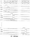
図3は、図1の動作を示す信号波形図である。以下、この図3を参照しつつ、図1の動作を説明する。 FIG. 3 is a signal waveform diagram showing the operation of FIG. The operation of FIG. 1 will be described below with reference to FIG.
基準電流生成部10において、基準電圧Vrefと基準抵抗Rrefで規定される基準電流Irefが生成され、この基準電流Irefに対応するバイアス電圧VBが出力されてDA変換部20に与えられ、DA変換部20において、与えられる表示データDinの値に応じた表示電流SNKが生成されてノードN2から出力されることは、従来通りである。 In the reference
表示データDinによって電流ラッチ部30A1に対応する値D1が出力されると、DA変換部20からこの値D1に対応する表示電流SNKが生成される。When the value D1 corresponding to a current latch portion 30A1 is output by the display data Din, display current SNK corresponding from the
一方、タイミング制御部40Aからは、表示データDinが値D1である期間の前半に、電流ラッチ部30A1に対してリセット信号R1が出力される。この時、書込制御信号SWA1,SWB1は出力されておらず、電流ラッチ部30A1のスイッチ31,32はオフである。これにより、電流ラッチ部30A1のNMOS36がオンとなり、ノードN4は接地電位GNDとなり、キャパシタ34は完全に放電される。また、NMOS35に流れる駆動電流OUT1は、0となる。On the other hand, the reset signal R1 is output from the
表示データDinが値D1である期間の後半には、タイミング制御部40Aから電流ラッチ部30A1に対して、リセット信号R1に代えて、書込制御信号SWA1,SWB1が出力される。これにより、電流ラッチ部30A1のNMOS36はオフ、スイッチ31,32がオンとなり、NMOS33,35による電流ミラー回路が構成される。DA変換部20から出力された表示電流SNKがNMOS33に流れると、これに応じて、NMOS35にも表示電流SNKと同じI1の大きさの駆動電流OUT1が流れる。また、キャパシタ34は、この時のNMOS35のゲート電圧に充電される。その後、書込制御信号SWB1が停止してスイッチ32がオフになり、続いて書込制御信号SWA1が停止してスイッチ31がオフになる。In the second half of the period the display data Din is the value D1, to the current latching part 30A1 from the
電流ラッチ部30A1では、書込制御信号SWA1,SWB1の停止により、NMOS33に流れる電流はなくなるが、キャパシタ34はD1×Irefの大きさの電流に対応するゲート電圧に充電されているので、NMOS35にはD1×Irefの大きさの駆動電流OUT1が流れ続ける。The current latching part 30A1, by stopping the write control signal SWA1, SWB1, but not the current flowing through the
次に、表示データDinによって電流ラッチ部30A2に対応する値D2が出力されると、DA変換部20からこの値D2に対応する表示電流SNKが生成され、電流ラッチ部30A2において、先の電流ラッチ部30A1と同様の動作が行われる。Next, the display when the value D2 corresponding to the current latching portion 30A2 is output by the data Din, display current SNK corresponding from the
同様の動作により、各電流ラッチ部30A1〜30AnのNMOS35に、それぞれ表示データDinの値D1〜Dnに対応する駆動電流OUT1〜OUTnが流れ続ける。By the same operation, the NMOS35 of each
以上のように、この実施例1の電流駆動回路は、各電流ラッチ部30Aiに、バイアス電圧保持用のキャパシタ34を放電させるためのNMOS36を設けると共に、これらの電流ラッチ部30iに書き込みを行う直前に、キャパシタ34を放電させるためのリセット信号Riを出力するタイミング制御部40Aを有している。これにより、キャパシタ34が完全に放電された状態で、新たな駆動電流OUTiに対応するバイアス電圧を書き込むことができるので、例えば次の表示データDinに対する駆動電流が0となった場合でも、精度良く駆動電流を保持することができるという利点がある。As described above, the current drive circuit of the first embodiment, each current latch section 30Ai, provided with a NMOS36 for discharging the
図4は、本発明の実施例2を示す電流駆動回路の構成図であり、図1中の要素と共通の要素には共通の符号が付されている。 FIG. 4 is a configuration diagram of a current driving circuit showing a second embodiment of the present invention. Elements common to those in FIG. 1 are denoted by common reference numerals.
この電流駆動回路は、図1と同様の基準電流生成部10及びDA変換部20と、図1とは若干構成の異なる複数の電流ラッチ部30B1〜30Bn及びタイミング制御部40Bと、新たに設けられたセット電圧生成部50を備えている。The current drive circuit includes a reference
各電流ラッチ部30B1〜30Bnは、いずれも同様の構成で、例えば電流ラッチ部30B1に示すように、DA変換部20内のノードN2とこの電流ラッチ部30B1内のノードN3の間に接続されたスイッチ31、ノードN3とノードN4の間に接続されたスイッチ32を有している。これらのスイッチ31,32は、タイミング制御部40Aから与えられる書込制御信号SWA1,SWB1によって、それぞれオン・オフ制御されるものである。Each
更に、電流ラッチ部30B1は、ノードN3にドレインとゲートが接続され、ソースが接地電位GNDに接続されたNMOS33、ノードN4と接地電位GNDの間に接続されたキャパシタ34、及びゲートとソースがそれぞれノードN4と接地電位GNDに接続されたNMOS35、ドレインがノードN4に接続され、ゲートにタイミング制御部40Aからセット信号S1が与えられ、ソースにはセット電圧VSTが与えられるNMOS37を有している。NMOS35のドレインは、表示装置1の対応する表示ラインに接続され、このNMOS35に流入する駆動電流OUT1によって表示装置1を駆動するようになっている。Furthermore, the current latch section 30B1 has a drain and a gate connected to node N3, a source connected to the ground
タイミング制御部40Bは、図1中のタイミング制御部40Aで出力するリセット信号R1〜Rnに代えて、同じタイミングのセット信号S1〜Snを出力するものである。 The
また、セット電圧生成部50は、表示データDinの値Diに応じたセット電圧VSTを生成し、各電流ラッチ部30B1〜30BnのNMOS37のソースに与えるものである。このセット電圧VSTは、表示データDinの値Diに応じた表示電流SNKに対応するNMOS35のゲート電圧、即ちバイアス電位とほぼ等しい電圧になっている。The
図5は、セット電圧生成部50の入出力関係の一例を示す特性図であり、横軸に入力される表示データDinの値、縦軸に出力するセット電圧VSTの大きさを示している。 FIG. 5 is a characteristic diagram showing an example of the input / output relationship of the set
即ち、このセット電圧生成部50は、表示データDinが値A以下の時はセット電圧VSTは0に固定され、表示データDinが値A〜値Bの間は一定の傾きで増加し、表示データDinが値B〜値Cの間はより大きな傾きで増加し、更に表示データDinが値C以上になると更に大きな傾きでセット電圧VSTが増加するように構成されている。 That is, when the display data Din is less than or equal to the value A, the set
このようなセット電圧生成部50は、抵抗分圧器と選択用のスイッチを組み合わせたり、メモリを用いた変換テーブルと直線的なDA変換器を組み合わせたりすることにより、構成することができる。 Such a set
図6は、図4の動作を示す信号波形図である。以下、この図6を参照しつつ、図4の動作を説明する。 FIG. 6 is a signal waveform diagram showing the operation of FIG. Hereinafter, the operation of FIG. 4 will be described with reference to FIG.
基準電流生成部10において、基準電圧Vrefと基準抵抗Rrefで規定される基準電流Irefが生成され、この基準電流Irefに対応するバイアス電圧VBが出力されてDA変換部20に与えられ、DA変換部20において、与えられる表示データDinの値に応じた表示電流SNKが生成されてノードN2から出力されることは、従来通りである。更に、表示データDinはセット電圧生成部60に与えられ、このセット電圧生成部60によって、表示データDinの値に対応したセット電圧VSTが出力される。 In the reference
一方、タイミング制御部40Bからは、表示データDinが値D1である期間の前半に、電流ラッチ部30B1に対してセット信号S1が出力される。この時、書込制御信号SWA1,SWB1は出力されておらず、電流ラッチ部30B1のスイッチ31,32はオフである。これにより、電流ラッチ部30B1のNMOS37がオンとなり、ノードN4にはセット電圧VSTが印加され、キャパシタ34はこのセット電圧VSTに充電される。セット電圧VSTは、表示データDinの値D1に応じた表示電流SNK(=I1)に対応するNMOS35のバイアス電位とほぼ等しい電圧に設定されているので、NMOS35には、ほぼI1の大きさの駆動電流OUT1が流れる。On the other hand, the
表示データDinが値D1である期間の後半には、タイミング制御部40Bから電流ラッチ部30B1に対して、セット信号S1に代えて、書込制御信号SWA1,SWB1が出力される。これにより、電流ラッチ部30B1のNMOS37はオフ、スイッチ31,32がオンとなり、DA変換部20から出力された表示電流SNKがNMOS33に流れる。これに応じて、NMOS35にも表示電流SNKと同じI1の大きさの駆動電流OUT1が流れる。また、キャパシタ34は、この時のNMOS35のゲート電圧に充電される。その後、書込制御信号SWB1が停止してスイッチ32がオフになり、続いて書込制御信号SWA1が停止してスイッチ31がオフになる。In the second half of the period the display data Din is the value D1, to the current latch section 30B1 from the
電流ラッチ部30B1では、書込制御信号SWA1,SWB1の停止により、NMOS33に流れる電流はなくなるが、キャパシタ34はI1(=D1×Iref)の大きさの電流に対応するゲート電圧に充電されているので、NMOS35にはD1×Irefの大きさの駆動電流OUT1が流れ続ける。In current latch section 30B1, by stopping the write control signal SWA1, SWB1, but not the current flowing through the
次に、表示データDinによって電流ラッチ部30B2に対応する値D2が出力されると、DA変換部20からこの値D2に対応する表示電流SNKが生成され、電流ラッチ部30B2において、先の電流ラッチ部30B1と同様の動作が行われる。Next, the display when the value D2 corresponding to the current latch section 30B2 are output by the data Din, display current SNK corresponding from the
同様の動作により、各電流ラッチ部30B1〜30BnのNMOS35に、それぞれ表示データDinの値D1〜Dnに対応する駆動電流OUT1〜OUTnが流れ続ける。By the same operation, the NMOS35 of each
以上のように、この実施例2の電流駆動回路は、表示データDinに応じた表示電流SNKに対応するNMOS35のゲート電圧にほぼ等しいセット電圧VSTを生成するセット電圧生成部50を設けると共に、各電流ラッチ部30B1〜30Bnには、タイミング制御部40Bから与えられるセット信号Siに従って、バイアス電圧保持用のキャパシタ34をセット電圧VSTに充電するためのNMOS37を設けている。これにより、実施例1と同様の利点に加えて、応答速度を更に向上することができるという利点がある。As described above, the current drive circuit according to the second embodiment includes the set
なお、本発明は、上記実施例に限定されず、種々の変形が可能である。この変形例としては、例えば、次のようなものがある。
(1) タイミング制御部40A,40Bから出力される書込制御信号SWAi,SWBi、リセット信号Ri及びセット信号Siのタイミングは、図3及び図6に例示したものに限定されない。例えば、図1の電流駆動回路において、表示データDinが値D1の時点で、次の電流ラッチ部30A2に対するリセット信号R2を事前に出力するように構成すれば、応答速度を更に向上することができる。
(2) セット電圧生成部50の入出力特性は、図5に例示したものに限定されない。例えば、表示データDinに対して階段状に変化するセット電圧VSTを出力したり、或いは一定の値を出力するように構成したりすることができる。
(3) 電流ラッチ部30A,30Bは、駆動電流OUTを吸い込むことで表示装置1を駆動する回路であるが、表示装置側へ駆動電流を供給する回路に対しても、同様に適用可能である。In addition, this invention is not limited to the said Example, A various deformation | transformation is possible. Examples of this modification include the following.
(1) The timings of the write control signals SWAi and SWBi, the reset signal Ri, and the set signal Si output from the
(2) The input / output characteristics of the set
(3) The current latch units 30A and 30B are circuits that drive the
1 表示装置
10 基準電流生成部
20 DA変換部
30A,30B 電流ラッチ部
31,32 スイッチ
33,35〜37 NMOS
34 キャパシタ
40A,40B タイミング制御部
50 セット電圧生成部DESCRIPTION OF
34
Claims (2)
Translated fromJapanese前記表示電流が出力される第1のノードと第2のノードとの間を第1の書込制御信号に従ってオン・オフする第1のスイッチと、
前記第2のノードにドレインとゲートが接続され、共通電位にソースが接続された第1のトランジスタと、
前記第2のノードと第3のノードの間を第2の書込制御信号に従ってオン・オフする第2のスイッチと、
前記第3のノードと前記共通電位の間に接続されて該第3のノードの電位を保持するキャパシタと、
前記第3のノードと前記共通電位の間に接続され、前記第1及び第2の書込制御信号に先立って与えられるリセット信号によってオン状態となる第2のトランジスタと、
前記第3のノードと前記共通電位にゲートとソースがそれぞれ接続され、ドレインから前記駆動電流を出力する第3のトランジスタとを、
備えたことを特徴とする電流駆動回路。A current driving circuit for holding a display current sequentially output from the display current generating means in accordance with a value of input data and outputting the display current as a driving current according to a write control signal;
A first switch for turning on and off according to a first write control signal between a first node and a second node from which the display current is output;
A first transistor having a drain and a gate connected to the second node and a source connected to a common potential;
A second switch that turns on and off between the second node and the third node according to a second write control signal;
A capacitor connected between the third node and the common potential to hold the potential of the third node;
A second transistor connected between the third node and the common potential and turned on by a reset signal applied prior to the first and second write control signals;
A third transistor having a gate and a source connected to the third node and the common potential and outputting the driving current from a drain;
A current driving circuit comprising:
前記表示電流が出力される第1のノードと第2のノードとの間を第1の書込制御信号に従ってオン・オフする第1のスイッチと、
前記第2のノードにドレインとゲートが接続され、共通電位にソースが接続された第1のトランジスタと、
前記第2のノードと第3のノードの間を第2の書込制御信号に従ってオン・オフする第2のスイッチと、
前記第3のノードと前記共通電位の間に接続されて該第3のノードの電位を保持するキャパシタと、
前記第3のノードと前記入力データの値に応じて生成されるバイアス電位の間に接続され、前記第1及び第2の書込制御信号に先立って与えられるセット信号によってオン状態となる第2のトランジスタと、
前記第3のノードと前記共通電位にゲートとソースがそれぞれ接続され、ドレインから前記駆動電流を出力する第3のトランジスタとを、
備えたことを特徴とする電流駆動回路。A current driving circuit for holding a display current sequentially output from the display current generating means in accordance with a value of input data and outputting the display current as a driving current according to a write control signal;
A first switch for turning on and off according to a first write control signal between a first node and a second node from which the display current is output;
A first transistor having a drain and a gate connected to the second node and a source connected to a common potential;
A second switch that turns on and off between the second node and the third node according to a second write control signal;
A capacitor connected between the third node and the common potential to hold the potential of the third node;
The second node is connected between the third node and a bias potential generated according to the value of the input data, and is turned on by a set signal given prior to the first and second write control signals. Transistors
A third transistor having a gate and a source connected to the third node and the common potential and outputting the driving current from a drain;
A current driving circuit comprising:
Priority Applications (4)
| Application Number | Priority Date | Filing Date | Title |
|---|---|---|---|
| JP2006060621AJP2007240698A (en) | 2006-03-07 | 2006-03-07 | Current drive circuit |
| US11/645,758US7859489B2 (en) | 2006-03-07 | 2006-12-27 | Current drive circuit for supplying driving current to display panel |
| CN2007100024203ACN101034541B (en) | 2006-03-07 | 2007-01-17 | Current drive circuit |
| KR1020070005599AKR20070092100A (en) | 2006-03-07 | 2007-01-18 | Current drive circuit |
Applications Claiming Priority (1)
| Application Number | Priority Date | Filing Date | Title |
|---|---|---|---|
| JP2006060621AJP2007240698A (en) | 2006-03-07 | 2006-03-07 | Current drive circuit |
Publications (1)
| Publication Number | Publication Date |
|---|---|
| JP2007240698Atrue JP2007240698A (en) | 2007-09-20 |
Family
ID=38478459
Family Applications (1)
| Application Number | Title | Priority Date | Filing Date |
|---|---|---|---|
| JP2006060621APendingJP2007240698A (en) | 2006-03-07 | 2006-03-07 | Current drive circuit |
Country Status (4)
| Country | Link |
|---|---|
| US (1) | US7859489B2 (en) |
| JP (1) | JP2007240698A (en) |
| KR (1) | KR20070092100A (en) |
| CN (1) | CN101034541B (en) |
Families Citing this family (9)
| Publication number | Priority date | Publication date | Assignee | Title |
|---|---|---|---|---|
| JP4439552B2 (en)* | 2007-10-04 | 2010-03-24 | Okiセミコンダクタ株式会社 | Current source device |
| JP4717091B2 (en)* | 2008-02-29 | 2011-07-06 | Okiセミコンダクタ株式会社 | Display panel drive device |
| JP5856799B2 (en) | 2011-10-17 | 2016-02-10 | ピクストロニクス,インコーポレイテッド | Latch circuit and display device |
| CN103198788A (en)* | 2013-03-06 | 2013-07-10 | 京东方科技集团股份有限公司 | Pixel circuit, organic electroluminescence display panel and display device |
| JP2015114652A (en)* | 2013-12-16 | 2015-06-22 | 双葉電子工業株式会社 | Display driving device, display driving method, and display device |
| CN104809988B (en)* | 2015-05-18 | 2016-06-29 | 京东方科技集团股份有限公司 | A kind of OLED array and display floater, display device |
| JP7176713B2 (en)* | 2017-11-29 | 2022-11-22 | 深▲セン▼通鋭微電子技術有限公司 | Signal level conversion circuit and display driving device |
| TWI699747B (en)* | 2019-04-26 | 2020-07-21 | 大陸商北京集創北方科技股份有限公司 | Drive current supply circuit, LED display drive device and LED display device |
| CN115348702B (en)* | 2022-09-06 | 2025-08-05 | 上海艾为电子技术股份有限公司 | Driving acceleration circuit, LED driving circuit and electronic equipment |
Citations (5)
| Publication number | Priority date | Publication date | Assignee | Title |
|---|---|---|---|---|
| JP2000221942A (en)* | 1999-01-29 | 2000-08-11 | Nec Corp | Organic el element driving device |
| JP2000310792A (en)* | 1999-04-27 | 2000-11-07 | Toshiba Corp | Liquid crystal display |
| JP2003177709A (en)* | 2001-12-13 | 2003-06-27 | Seiko Epson Corp | Pixel circuit for light emitting element |
| JP2003195815A (en)* | 2000-11-07 | 2003-07-09 | Sony Corp | Active matrix type display device and active matrix type organic electroluminescence display device |
| JP2004252419A (en)* | 2002-11-29 | 2004-09-09 | Semiconductor Energy Lab Co Ltd | Current driving circuit and display device using the same |
Family Cites Families (4)
| Publication number | Priority date | Publication date | Assignee | Title |
|---|---|---|---|---|
| JP3564347B2 (en)* | 1999-02-19 | 2004-09-08 | 株式会社東芝 | Display device driving circuit and liquid crystal display device |
| JP3970110B2 (en)* | 2002-06-27 | 2007-09-05 | カシオ計算機株式会社 | CURRENT DRIVE DEVICE, ITS DRIVE METHOD, AND DISPLAY DEVICE USING CURRENT DRIVE DEVICE |
| JP4074995B2 (en) | 2003-06-16 | 2008-04-16 | カシオ計算機株式会社 | CURRENT DRIVE CIRCUIT, CONTROL METHOD THEREOF, AND DISPLAY DEVICE PROVIDED WITH THE CURRENT DRIVE CIRCUIT |
| JP2005099712A (en)* | 2003-08-28 | 2005-04-14 | Sharp Corp | Display device drive circuit and display device |
- 2006
- 2006-03-07JPJP2006060621Apatent/JP2007240698A/enactivePending
- 2006-12-27USUS11/645,758patent/US7859489B2/ennot_activeExpired - Fee Related
- 2007
- 2007-01-17CNCN2007100024203Apatent/CN101034541B/ennot_activeExpired - Fee Related
- 2007-01-18KRKR1020070005599Apatent/KR20070092100A/ennot_activeCeased
Patent Citations (5)
| Publication number | Priority date | Publication date | Assignee | Title |
|---|---|---|---|---|
| JP2000221942A (en)* | 1999-01-29 | 2000-08-11 | Nec Corp | Organic el element driving device |
| JP2000310792A (en)* | 1999-04-27 | 2000-11-07 | Toshiba Corp | Liquid crystal display |
| JP2003195815A (en)* | 2000-11-07 | 2003-07-09 | Sony Corp | Active matrix type display device and active matrix type organic electroluminescence display device |
| JP2003177709A (en)* | 2001-12-13 | 2003-06-27 | Seiko Epson Corp | Pixel circuit for light emitting element |
| JP2004252419A (en)* | 2002-11-29 | 2004-09-09 | Semiconductor Energy Lab Co Ltd | Current driving circuit and display device using the same |
Also Published As
| Publication number | Publication date |
|---|---|
| KR20070092100A (en) | 2007-09-12 |
| US20070211043A1 (en) | 2007-09-13 |
| US7859489B2 (en) | 2010-12-28 |
| CN101034541B (en) | 2010-12-29 |
| CN101034541A (en) | 2007-09-12 |
Similar Documents
| Publication | Publication Date | Title |
|---|---|---|
| US10777119B2 (en) | Semiconductor device | |
| JP2007240698A (en) | Current drive circuit | |
| TWI342544B (en) | Shift register | |
| US6885723B2 (en) | Shift-register circuit | |
| US20070001985A1 (en) | Display device | |
| US9721526B2 (en) | Display driver with small-area level shift circuit | |
| JP4241466B2 (en) | Differential amplifier, digital / analog converter and display device | |
| US7468621B2 (en) | Synchronization circuits and methods | |
| JP2007089074A (en) | Differential amplifier, digital-analog converter and display device | |
| JPWO2018055666A1 (en) | Interface circuit | |
| TWI625711B (en) | Gate driving circuit | |
| JP2007227990A (en) | Timing generating circuit and d/a converter using the same | |
| US20050141306A1 (en) | Memory device | |
| CN101154360A (en) | Image display system and method of driving display module | |
| JPH11308092A (en) | Level shift circuit and nonvolatile memory provided with the same | |
| JP2007194771A (en) | Level conversion circuit and display apparatus | |
| JP2005311790A (en) | Signal level conversion circuit and liquid crystal display device using this circuit | |
| JP2010232848A (en) | Start-up circuit for internal power supply of semiconductor memory | |
| JP2000151408A (en) | Current cell and d/a converter employing it | |
| JP4630782B2 (en) | Level shift circuit | |
| JP2007060344A (en) | Level shift circuit | |
| US7088165B2 (en) | Voltage level shifter and sequential pulse generator | |
| JP4565918B2 (en) | Shift register circuit and bidirectional shift register circuit | |
| US20060055448A1 (en) | Voltage generator | |
| JP2009225083A (en) | Differential control circuit |
Legal Events
| Date | Code | Title | Description |
|---|---|---|---|
| A621 | Written request for application examination | Free format text:JAPANESE INTERMEDIATE CODE: A621 Effective date:20080729 | |
| A711 | Notification of change in applicant | Free format text:JAPANESE INTERMEDIATE CODE: A712 Effective date:20081210 | |
| RD02 | Notification of acceptance of power of attorney | Free format text:JAPANESE INTERMEDIATE CODE: A7422 Effective date:20090420 | |
| A131 | Notification of reasons for refusal | Free format text:JAPANESE INTERMEDIATE CODE: A131 Effective date:20110524 | |
| A02 | Decision of refusal | Free format text:JAPANESE INTERMEDIATE CODE: A02 Effective date:20111004 |