JP2007237718A - Inkjet head manufacturing method - Google Patents
Inkjet head manufacturing methodDownload PDFInfo
- Publication number
- JP2007237718A JP2007237718AJP2006067429AJP2006067429AJP2007237718AJP 2007237718 AJP2007237718 AJP 2007237718AJP 2006067429 AJP2006067429 AJP 2006067429AJP 2006067429 AJP2006067429 AJP 2006067429AJP 2007237718 AJP2007237718 AJP 2007237718A
- Authority
- JP
- Japan
- Prior art keywords
- pressure chamber
- substrate
- manufacturing
- actuator
- ink
- Prior art date
- Legal status (The legal status is an assumption and is not a legal conclusion. Google has not performed a legal analysis and makes no representation as to the accuracy of the status listed.)
- Pending
Links
- 238000004519manufacturing processMethods0.000titleclaimsabstractdescription50
- 238000000034methodMethods0.000claimsabstractdescription79
- 239000000758substrateSubstances0.000claimsabstractdescription68
- 239000007791liquid phaseSubstances0.000claimsabstractdescription8
- 238000007599dischargingMethods0.000claimsabstractdescription6
- XUIMIQQOPSSXEZ-UHFFFAOYSA-NSiliconChemical compound[Si]XUIMIQQOPSSXEZ-UHFFFAOYSA-N0.000claimsdescription41
- 229910052710siliconInorganic materials0.000claimsdescription41
- 239000010703siliconSubstances0.000claimsdescription41
- 238000005323electroformingMethods0.000claimsdescription9
- 238000005498polishingMethods0.000claimsdescription9
- 229910000990Ni alloyInorganic materials0.000claimsdescription7
- 239000000126substanceSubstances0.000claimsdescription6
- 239000012071phaseSubstances0.000claimsdescription3
- 230000002950deficientEffects0.000abstractdescription23
- 239000012808vapor phaseSubstances0.000abstractdescription5
- 239000010408filmSubstances0.000description47
- 239000000976inkSubstances0.000description38
- 230000008569processEffects0.000description26
- BASFCYQUMIYNBI-UHFFFAOYSA-NplatinumChemical compound[Pt]BASFCYQUMIYNBI-UHFFFAOYSA-N0.000description18
- 239000010410layerSubstances0.000description17
- 239000000047productSubstances0.000description16
- VYPSYNLAJGMNEJ-UHFFFAOYSA-NSilicium dioxideChemical compoundO=[Si]=OVYPSYNLAJGMNEJ-UHFFFAOYSA-N0.000description10
- MCMNRKCIXSYSNV-UHFFFAOYSA-NZirconium dioxideChemical compoundO=[Zr]=OMCMNRKCIXSYSNV-UHFFFAOYSA-N0.000description10
- PXHVJJICTQNCMI-UHFFFAOYSA-NnickelSubstances[Ni]PXHVJJICTQNCMI-UHFFFAOYSA-N0.000description10
- 229910052814silicon oxideInorganic materials0.000description10
- 229910052697platinumInorganic materials0.000description9
- 230000001681protective effectEffects0.000description9
- 239000004065semiconductorSubstances0.000description7
- 230000007547defectEffects0.000description6
- 229910052751metalInorganic materials0.000description6
- 239000002184metalSubstances0.000description6
- 229910052759nickelInorganic materials0.000description6
- 238000007789sealingMethods0.000description6
- 238000004544sputter depositionMethods0.000description6
- 238000004891communicationMethods0.000description5
- 238000005530etchingMethods0.000description5
- 238000009792diffusion processMethods0.000description4
- 238000007689inspectionMethods0.000description4
- 230000015572biosynthetic processEffects0.000description3
- 238000007796conventional methodMethods0.000description3
- 238000010438heat treatmentMethods0.000description3
- 239000011229interlayerSubstances0.000description3
- 230000009467reductionEffects0.000description3
- 238000003980solgel methodMethods0.000description3
- 229910052726zirconiumInorganic materials0.000description3
- 229910004298SiO 2Inorganic materials0.000description2
- 229910003134ZrOxInorganic materials0.000description2
- 229910045601alloyInorganic materials0.000description2
- 239000000956alloySubstances0.000description2
- 230000008859changeEffects0.000description2
- 238000006243chemical reactionMethods0.000description2
- 238000011161developmentMethods0.000description2
- 230000000694effectsEffects0.000description2
- 239000007789gasSubstances0.000description2
- 238000005304joiningMethods0.000description2
- 239000000463materialSubstances0.000description2
- BPUBBGLMJRNUCC-UHFFFAOYSA-Noxygen(2-);tantalum(5+)Chemical compound[O-2].[O-2].[O-2].[O-2].[O-2].[Ta+5].[Ta+5]BPUBBGLMJRNUCC-UHFFFAOYSA-N0.000description2
- RVTZCBVAJQQJTK-UHFFFAOYSA-Noxygen(2-);zirconium(4+)Chemical compound[O-2].[O-2].[Zr+4]RVTZCBVAJQQJTK-UHFFFAOYSA-N0.000description2
- 238000001020plasma etchingMethods0.000description2
- 238000007747platingMethods0.000description2
- 239000002904solventSubstances0.000description2
- 229910001936tantalum oxideInorganic materials0.000description2
- 239000010409thin filmSubstances0.000description2
- 229910052719titaniumInorganic materials0.000description2
- 229910001928zirconium oxideInorganic materials0.000description2
- 229910018072Al 2 O 3Inorganic materials0.000description1
- 229910017107AlOxInorganic materials0.000description1
- 241000877463LanioSpecies0.000description1
- 229910004121SrRuOInorganic materials0.000description1
- 229910003087TiOxInorganic materials0.000description1
- QCWXUUIWCKQGHC-UHFFFAOYSA-NZirconiumChemical compound[Zr]QCWXUUIWCKQGHC-UHFFFAOYSA-N0.000description1
- 230000009471actionEffects0.000description1
- 230000004913activationEffects0.000description1
- 239000000853adhesiveSubstances0.000description1
- 230000001070adhesive effectEffects0.000description1
- 239000012790adhesive layerSubstances0.000description1
- 150000004703alkoxidesChemical class0.000description1
- 229910052782aluminiumInorganic materials0.000description1
- 238000000137annealingMethods0.000description1
- 230000004888barrier functionEffects0.000description1
- 238000005452bendingMethods0.000description1
- 238000009835boilingMethods0.000description1
- 239000000919ceramicSubstances0.000description1
- 238000005229chemical vapour depositionMethods0.000description1
- 238000000576coating methodMethods0.000description1
- 150000001875compoundsChemical class0.000description1
- 239000000470constituentSubstances0.000description1
- 230000007797corrosionEffects0.000description1
- 238000005260corrosionMethods0.000description1
- 238000002425crystallisationMethods0.000description1
- 230000008025crystallizationEffects0.000description1
- 230000007423decreaseEffects0.000description1
- 238000010586diagramMethods0.000description1
- 239000006185dispersionSubstances0.000description1
- 239000002612dispersion mediumSubstances0.000description1
- 238000001312dry etchingMethods0.000description1
- 238000009713electroplatingMethods0.000description1
- 239000012467final productSubstances0.000description1
- 238000010304firingMethods0.000description1
- 239000011521glassSubstances0.000description1
- 229910052737goldInorganic materials0.000description1
- 230000020169heat generationEffects0.000description1
- 239000001257hydrogenSubstances0.000description1
- 229910052739hydrogenInorganic materials0.000description1
- 238000001027hydrothermal synthesisMethods0.000description1
- 229910052745leadInorganic materials0.000description1
- 239000011344liquid materialSubstances0.000description1
- 238000002488metal-organic chemical vapour depositionMethods0.000description1
- 150000002739metalsChemical class0.000description1
- 238000012986modificationMethods0.000description1
- 230000004048modificationEffects0.000description1
- 150000002894organic compoundsChemical class0.000description1
- TWNQGVIAIRXVLR-UHFFFAOYSA-Noxo(oxoalumanyloxy)alumaneChemical compoundO=[Al]O[Al]=OTWNQGVIAIRXVLR-UHFFFAOYSA-N0.000description1
- 238000000059patterningMethods0.000description1
- 238000009832plasma treatmentMethods0.000description1
- 229920001296polysiloxanePolymers0.000description1
- 238000012545processingMethods0.000description1
- VSZWPYCFIRKVQL-UHFFFAOYSA-Nselanylidenegallium;seleniumChemical compound[Se].[Se]=[Ga].[Se]=[Ga]VSZWPYCFIRKVQL-UHFFFAOYSA-N0.000description1
- 239000002344surface layerSubstances0.000description1
- HLLICFJUWSZHRJ-UHFFFAOYSA-NtioxidazoleChemical compoundCCCOC1=CC=C2N=C(NC(=O)OC)SC2=C1HLLICFJUWSZHRJ-UHFFFAOYSA-N0.000description1
- 238000012546transferMethods0.000description1
- WFKWXMTUELFFGS-UHFFFAOYSA-NtungstenChemical compound[W]WFKWXMTUELFFGS-UHFFFAOYSA-N0.000description1
- 229910052721tungstenInorganic materials0.000description1
- 239000010937tungstenSubstances0.000description1
- 238000007740vapor depositionMethods0.000description1
Images


Classifications
- B—PERFORMING OPERATIONS; TRANSPORTING
- B41—PRINTING; LINING MACHINES; TYPEWRITERS; STAMPS
- B41J—TYPEWRITERS; SELECTIVE PRINTING MECHANISMS, i.e. MECHANISMS PRINTING OTHERWISE THAN FROM A FORME; CORRECTION OF TYPOGRAPHICAL ERRORS
- B41J2/00—Typewriters or selective printing mechanisms characterised by the printing or marking process for which they are designed
- B41J2/005—Typewriters or selective printing mechanisms characterised by the printing or marking process for which they are designed characterised by bringing liquid or particles selectively into contact with a printing material
- B41J2/01—Ink jet
- B41J2/135—Nozzles
- B41J2/16—Production of nozzles
- B41J2/1607—Production of print heads with piezoelectric elements
- B41J2/161—Production of print heads with piezoelectric elements of film type, deformed by bending and disposed on a diaphragm
- B—PERFORMING OPERATIONS; TRANSPORTING
- B41—PRINTING; LINING MACHINES; TYPEWRITERS; STAMPS
- B41J—TYPEWRITERS; SELECTIVE PRINTING MECHANISMS, i.e. MECHANISMS PRINTING OTHERWISE THAN FROM A FORME; CORRECTION OF TYPOGRAPHICAL ERRORS
- B41J2/00—Typewriters or selective printing mechanisms characterised by the printing or marking process for which they are designed
- B41J2/005—Typewriters or selective printing mechanisms characterised by the printing or marking process for which they are designed characterised by bringing liquid or particles selectively into contact with a printing material
- B41J2/01—Ink jet
- B41J2/135—Nozzles
- B41J2/16—Production of nozzles
- B41J2/1621—Manufacturing processes
- B41J2/1626—Manufacturing processes etching
- B41J2/1628—Manufacturing processes etching dry etching
- B—PERFORMING OPERATIONS; TRANSPORTING
- B41—PRINTING; LINING MACHINES; TYPEWRITERS; STAMPS
- B41J—TYPEWRITERS; SELECTIVE PRINTING MECHANISMS, i.e. MECHANISMS PRINTING OTHERWISE THAN FROM A FORME; CORRECTION OF TYPOGRAPHICAL ERRORS
- B41J2/00—Typewriters or selective printing mechanisms characterised by the printing or marking process for which they are designed
- B41J2/005—Typewriters or selective printing mechanisms characterised by the printing or marking process for which they are designed characterised by bringing liquid or particles selectively into contact with a printing material
- B41J2/01—Ink jet
- B41J2/135—Nozzles
- B41J2/16—Production of nozzles
- B41J2/1621—Manufacturing processes
- B41J2/1626—Manufacturing processes etching
- B41J2/1629—Manufacturing processes etching wet etching
- B—PERFORMING OPERATIONS; TRANSPORTING
- B41—PRINTING; LINING MACHINES; TYPEWRITERS; STAMPS
- B41J—TYPEWRITERS; SELECTIVE PRINTING MECHANISMS, i.e. MECHANISMS PRINTING OTHERWISE THAN FROM A FORME; CORRECTION OF TYPOGRAPHICAL ERRORS
- B41J2/00—Typewriters or selective printing mechanisms characterised by the printing or marking process for which they are designed
- B41J2/005—Typewriters or selective printing mechanisms characterised by the printing or marking process for which they are designed characterised by bringing liquid or particles selectively into contact with a printing material
- B41J2/01—Ink jet
- B41J2/135—Nozzles
- B41J2/16—Production of nozzles
- B41J2/1621—Manufacturing processes
- B41J2/1631—Manufacturing processes photolithography
- B—PERFORMING OPERATIONS; TRANSPORTING
- B41—PRINTING; LINING MACHINES; TYPEWRITERS; STAMPS
- B41J—TYPEWRITERS; SELECTIVE PRINTING MECHANISMS, i.e. MECHANISMS PRINTING OTHERWISE THAN FROM A FORME; CORRECTION OF TYPOGRAPHICAL ERRORS
- B41J2/00—Typewriters or selective printing mechanisms characterised by the printing or marking process for which they are designed
- B41J2/005—Typewriters or selective printing mechanisms characterised by the printing or marking process for which they are designed characterised by bringing liquid or particles selectively into contact with a printing material
- B41J2/01—Ink jet
- B41J2/135—Nozzles
- B41J2/16—Production of nozzles
- B41J2/1621—Manufacturing processes
- B41J2/1632—Manufacturing processes machining
- B41J2/1634—Manufacturing processes machining laser machining
- B—PERFORMING OPERATIONS; TRANSPORTING
- B41—PRINTING; LINING MACHINES; TYPEWRITERS; STAMPS
- B41J—TYPEWRITERS; SELECTIVE PRINTING MECHANISMS, i.e. MECHANISMS PRINTING OTHERWISE THAN FROM A FORME; CORRECTION OF TYPOGRAPHICAL ERRORS
- B41J2/00—Typewriters or selective printing mechanisms characterised by the printing or marking process for which they are designed
- B41J2/005—Typewriters or selective printing mechanisms characterised by the printing or marking process for which they are designed characterised by bringing liquid or particles selectively into contact with a printing material
- B41J2/01—Ink jet
- B41J2/135—Nozzles
- B41J2/16—Production of nozzles
- B41J2/1621—Manufacturing processes
- B41J2/164—Manufacturing processes thin film formation
- B41J2/1642—Manufacturing processes thin film formation thin film formation by CVD [chemical vapor deposition]
- B—PERFORMING OPERATIONS; TRANSPORTING
- B41—PRINTING; LINING MACHINES; TYPEWRITERS; STAMPS
- B41J—TYPEWRITERS; SELECTIVE PRINTING MECHANISMS, i.e. MECHANISMS PRINTING OTHERWISE THAN FROM A FORME; CORRECTION OF TYPOGRAPHICAL ERRORS
- B41J2/00—Typewriters or selective printing mechanisms characterised by the printing or marking process for which they are designed
- B41J2/005—Typewriters or selective printing mechanisms characterised by the printing or marking process for which they are designed characterised by bringing liquid or particles selectively into contact with a printing material
- B41J2/01—Ink jet
- B41J2/135—Nozzles
- B41J2/16—Production of nozzles
- B41J2/1621—Manufacturing processes
- B41J2/164—Manufacturing processes thin film formation
- B41J2/1643—Manufacturing processes thin film formation thin film formation by plating
- B—PERFORMING OPERATIONS; TRANSPORTING
- B41—PRINTING; LINING MACHINES; TYPEWRITERS; STAMPS
- B41J—TYPEWRITERS; SELECTIVE PRINTING MECHANISMS, i.e. MECHANISMS PRINTING OTHERWISE THAN FROM A FORME; CORRECTION OF TYPOGRAPHICAL ERRORS
- B41J2/00—Typewriters or selective printing mechanisms characterised by the printing or marking process for which they are designed
- B41J2/005—Typewriters or selective printing mechanisms characterised by the printing or marking process for which they are designed characterised by bringing liquid or particles selectively into contact with a printing material
- B41J2/01—Ink jet
- B41J2/135—Nozzles
- B41J2/16—Production of nozzles
- B41J2/1621—Manufacturing processes
- B41J2/164—Manufacturing processes thin film formation
- B41J2/1646—Manufacturing processes thin film formation thin film formation by sputtering
- Y—GENERAL TAGGING OF NEW TECHNOLOGICAL DEVELOPMENTS; GENERAL TAGGING OF CROSS-SECTIONAL TECHNOLOGIES SPANNING OVER SEVERAL SECTIONS OF THE IPC; TECHNICAL SUBJECTS COVERED BY FORMER USPC CROSS-REFERENCE ART COLLECTIONS [XRACs] AND DIGESTS
- Y10—TECHNICAL SUBJECTS COVERED BY FORMER USPC
- Y10T—TECHNICAL SUBJECTS COVERED BY FORMER US CLASSIFICATION
- Y10T29/00—Metal working
- Y10T29/42—Piezoelectric device making
- Y—GENERAL TAGGING OF NEW TECHNOLOGICAL DEVELOPMENTS; GENERAL TAGGING OF CROSS-SECTIONAL TECHNOLOGIES SPANNING OVER SEVERAL SECTIONS OF THE IPC; TECHNICAL SUBJECTS COVERED BY FORMER USPC CROSS-REFERENCE ART COLLECTIONS [XRACs] AND DIGESTS
- Y10—TECHNICAL SUBJECTS COVERED BY FORMER USPC
- Y10T—TECHNICAL SUBJECTS COVERED BY FORMER US CLASSIFICATION
- Y10T29/00—Metal working
- Y10T29/49—Method of mechanical manufacture
- Y10T29/49401—Fluid pattern dispersing device making, e.g., ink jet
Landscapes
- Engineering & Computer Science (AREA)
- Manufacturing & Machinery (AREA)
- Physics & Mathematics (AREA)
- Optics & Photonics (AREA)
- Particle Formation And Scattering Control In Inkjet Printers (AREA)
Abstract
Translated fromJapaneseDescription
Translated fromJapanese本発明は、インクを吐出するインクジェットヘッドの製造方法に関する。 The present invention relates to a method for manufacturing an inkjet head that ejects ink.
従来、インクジェット式プリンターなどに用いられるインクジェットヘッドとして、ピエゾ方式(圧電方式)のものやバブル方式(サーマル方式)のものなどが知られている。このようなインクジェットヘッドは、インクを貯留する圧力室を有し、この圧力室内のインクを、ピエゾ方式ではアクチュエーターによって、バブル方式では溶媒を沸騰させることにより発生した気泡によって押し出し、吐出させる機構となっている。 2. Description of the Related Art Conventionally, as an inkjet head used for an inkjet printer or the like, a piezoelectric method (piezoelectric method) or a bubble method (thermal method) is known. Such an ink jet head has a pressure chamber for storing ink, and the ink in the pressure chamber is pushed out by an actuator in the piezo method and discharged by bubbles generated by boiling the solvent in the bubble method. ing.
このようなインクジェットヘッドでは、例えば前記のピエゾ方式やバブル方式のものなどでも、圧力室を、半導体プロセスでシリコン基板(シリコンウエハ)に形成するのが一般的である。圧力室をシリコン基板に形成する理由としては、シリコン基板(シリコンウエハ)は加工が比較的容易であり、圧力室を精度よく作製できることが挙げられる。また、特にバブル方式のインクジェットヘッドでは、ヒータの形成が容易であり、かつヒータによる加熱に十分耐え得る耐熱性があることも理由として挙げられる。 In such an ink jet head, for example, in the piezo method or bubble method, the pressure chamber is generally formed on a silicon substrate (silicon wafer) by a semiconductor process. The reason why the pressure chamber is formed on the silicon substrate is that the silicon substrate (silicon wafer) is relatively easy to process and the pressure chamber can be manufactured with high accuracy. In particular, in the bubble-type ink jet head, the heater can be easily formed, and the heat resistance is sufficient to withstand the heating by the heater.
ところで、このようなシリコン基板(シリコンウエハ)を用いた半導体プロセスでは、製造コストを下げるために異物・欠陥等による不良率を下げ、歩留まりを上げることが必要であるが、この歩留まりにはチップサイズが大きく影響する。ところが、一般に、このインクジェットヘッドを形成するための要素となるヘッド用チップは所望のノズル数を確保しようとした場合、ICチップに比べて大きく本質的に歩留まりが困難である。 By the way, in the semiconductor process using such a silicon substrate (silicon wafer), it is necessary to reduce the defect rate due to foreign matter / defects and the like in order to reduce the manufacturing cost, and to increase the yield. Greatly affects. However, in general, a head chip, which is an element for forming the ink jet head, is larger than an IC chip and inherently difficult to obtain when it is desired to secure a desired number of nozzles.
例えば、現在、最も高密度化されたヘッドでも600dpi(ノズルピッチ42.3μm)であり、これを構成する1チップのサイズは、ICチップと比較して大型となる。したがって、一枚のシリコン基板(シリコンウエハ)から得られるヘッド用チップは、ICチップの場合に比べて少なくなり、よって良品としてのヘッド用チップの絶対数を確保するためには、ICチップの場合よりもさらに歩留まりを高くする必要があるのである。 For example, even the head with the highest density at present is 600 dpi (nozzle pitch 42.3 μm), and the size of one chip constituting this head is larger than that of an IC chip. Therefore, the number of head chips obtained from a single silicon substrate (silicon wafer) is smaller than that of an IC chip. Therefore, in order to ensure the absolute number of good head chips, the case of an IC chip is used. It is necessary to further increase the yield.
ところで、前述したように例えばピエゾ方式のインクジェットヘッドでは、従来、圧力室のみをシリコンウエハにより形成し、PZT等の圧電薄膜を有したアクチュエーターなど、他の部品をこれに貼り付けていくことで、ヘッドを組み立てる製造方法が主流であった。しかし、この製造方法では、圧力室以外の部品についての加工精度に問題があるため、高密度化に限界がある。 By the way, as described above, for example, in a piezo-type inkjet head, conventionally, only a pressure chamber is formed of a silicon wafer, and other parts such as an actuator having a piezoelectric thin film such as PZT are attached to this, The manufacturing method for assembling the head was mainstream. However, in this manufacturing method, there is a problem in processing accuracy for parts other than the pressure chamber, and thus there is a limit to increasing the density.
したがって、近年では、アクチュエーターやこれに接続する配線などを基板上に直接形成する、MEMS(micro electro mechanical systems)による製造方法が開発されている。この製造方法では、基板上にアクチュエーターや配線などを形成し、その後、同じ基板を加工して圧力室を形成し、さらに必要に応じて基板を個片化(ダイシング)することにより、インクジェットヘッドの構成要素となるヘッド用チップを作製している(例えば、特許文献1参照)。 Therefore, in recent years, a manufacturing method using MEMS (micro electro mechanical systems) has been developed in which an actuator and wiring connected thereto are directly formed on a substrate. In this manufacturing method, an actuator, wiring, and the like are formed on a substrate, and then the same substrate is processed to form a pressure chamber. Further, the substrate is separated into pieces (dicing) as necessary, so that the inkjet head A head chip which is a constituent element is manufactured (for example, see Patent Document 1).
このような製造方法にあっては、PZTなどの圧電薄膜(圧電体膜)を気相法、又は液相法で作製する際、結晶化のためのアニール温度が例えば600℃程度にまでなることから、基板としては少なくとも600℃以上の耐熱性を有していることが必須となる。そこで、基板としてシリコン(シリコンウエハ)を用いれば、耐熱性の点で問題がなく、しかも、前述したように圧力室を容易にかつ高精度で形成できるといった利点もそのまま有したものとなり、非常に合理的である。
しかしながら、この製造方法では、圧力室のみをシリコン基板から形成する従来法に比べ、シリコン基板に対してアクチュエーターやこれに接続する配線等を形成する工程が追加されるため、シリコン基板でのプロセス部分が長くなり、したがって異物や欠陥等による不良の発生が起こり易くなる。その結果、一枚のシリコン基板(シリコンウエハ)から得られるヘッド用チップの良品の数、すなわち歩留まりが十分に得られなくなってしまい、前述したように良品としてのヘッド用チップの絶対数が十分に確保できなくなり、製造コストの低減化が大きく妨げられていた。 However, in this manufacturing method, compared to the conventional method in which only the pressure chamber is formed from a silicon substrate, a process for forming an actuator and wiring connected to the silicon substrate is added. Therefore, the occurrence of defects due to foreign matters or defects is likely to occur. As a result, the number of non-defective head chips obtained from a single silicon substrate (silicon wafer), that is, the yield cannot be obtained sufficiently, and as described above, the absolute number of non-defective head chips is sufficient. As a result, it was impossible to ensure the production cost, which greatly hindered the reduction in manufacturing cost.
本発明は前記事情に鑑みてなされたもので、その目的とするところは、良品としてのヘッド用チップの歩留まりを上げ、その絶対数を十分に確保するようにし、これによって製造コストの低減化を可能にした、インクジェットヘッドの製造方法を提供することにある。 The present invention has been made in view of the above circumstances, and its object is to increase the yield of head chips as good products and to ensure a sufficient absolute number thereof, thereby reducing the manufacturing cost. An object of the present invention is to provide an ink jet head manufacturing method that is made possible.
前記目的を達成するため本発明のインクジェットヘッドの製造方法は、インクを貯留する圧力室と、該圧力室に設けられて前記インクを吐出するためのノズルと、前記圧力室の内圧を変化させ、前記ノズルから該圧力室内のインクを吐出させるためのアクチュエーターと、を具備してなるインクジェットヘッドの製造方法において、
基板上に液相法又は気相法を用いて前記アクチュエーターを形成し、上部構造体を製造する工程と、
前記基板から前記上部構造体を分離する工程と、
前記基板とは別に、圧力室を有する下部構造体を形成する工程と、
前記上部構造体と前記下部構造体とを接合する工程と、を備えたことを特徴としている。In order to achieve the above object, a method of manufacturing an inkjet head according to the present invention includes a pressure chamber for storing ink, a nozzle provided in the pressure chamber for discharging the ink, and an internal pressure of the pressure chamber, An actuator for discharging ink in the pressure chamber from the nozzle, and an inkjet head manufacturing method comprising:
Forming the actuator on a substrate using a liquid phase method or a gas phase method, and manufacturing an upper structure;
Separating the upper structure from the substrate;
Forming a lower structure having a pressure chamber separately from the substrate;
And a step of joining the upper structure and the lower structure.
このインクジェットヘッドの製造方法によれば、アクチュエーターを含む上部構造体と圧力室を有する下部構造体とを、同一の基板から形成することなくそれぞれ別に形成し、これらを接合して例えばインクジェットヘッドの構成要素となるヘッド用チップを形成するので、予め検査して良品と判定された上部構造体と、別に検査して良品と判定された下部構造体とを接合することで、前記ヘッド用チップの良品率(歩留まり)を上げ、その絶対数を十分に確保することができる。
すなわち、シリコン基板上にアクチュエーターやこれに接続する配線などを直接形成し、さらに同一のシリコン基板に圧力室も形成する従来法では、多くの工程を経てアクチュエーターや配線などを形成した後、圧力室を形成した際に、例えば異物や欠陥等に起因してこの圧力室に不良が発生すると、その上に形成された正常なアクチュエーターや配線なども、結果的に不良品の一部となってしまう。したがって、この正常なアクチュエーターや配線などは、最終的な製品に供されることができなくなり、そのため歩留まりが大きく低下し、製造コストの低減化が妨げられていた。
これに対し、本発明によれば、前述したように良品と判定された正常な上部構造体は、同じく良品と判定された下部構造体と接合されるようになるので、正常であるにもかかわらず不良品となってしまうといった不都合がなく、したがって、前述したように前記ヘッド用チップの良品率(歩留まり)が上がり、その絶対数も十分に確保できることにより、製造コストの低減化が可能になる。
また、高温プロセスを含むインクジェットヘッドの上部構造体の製造工程と、低温プロセスからなる下部構造体の形成工程とを、連続させることなく別にしているので、工程管理が容易になり、したがって生産性の向上を図ることが可能になる。According to this inkjet head manufacturing method, an upper structure including an actuator and a lower structure having a pressure chamber are formed separately from each other without being formed from the same substrate, and are joined to each other, for example, the configuration of an inkjet head Since the head chip as an element is formed, the upper structure that has been inspected in advance and determined to be non-defective is joined to the lower structure that has been inspected separately and determined to be non-defective, whereby the non-defective head chip The rate (yield) can be increased and the absolute number can be sufficiently secured.
That is, in the conventional method in which an actuator or wiring connected to the actuator is directly formed on a silicon substrate, and a pressure chamber is also formed on the same silicon substrate, the actuator and wiring are formed through many processes, and then the pressure chamber is formed. When a failure occurs in the pressure chamber due to, for example, foreign matter or a defect, a normal actuator or wiring formed thereon becomes a part of the defective product. . Therefore, these normal actuators and wiring cannot be used for the final product, so that the yield is greatly reduced, and the reduction of the manufacturing cost is hindered.
On the other hand, according to the present invention, the normal upper structure determined to be non-defective as described above is joined to the lower structure that is also determined to be non-defective. Therefore, there is no inconvenience that the product becomes a defective product. Therefore, as described above, the non-defective product rate (yield) of the head chip is increased, and the absolute number can be sufficiently secured, so that the manufacturing cost can be reduced. .
In addition, the manufacturing process of the upper structure of the inkjet head including the high temperature process and the forming process of the lower structure consisting of the low temperature process are separated without being continuous, so that the process management becomes easy, and thus the productivity. Can be improved.
また、前記インクジェットヘッドの製造方法においては、前記アクチュエーターが、PZT等の圧電体素子からなるものが好ましい。
圧電体素子でアクチュエーターを構成することにより、インクの吐出駆動を精度良く行わせることができるうえ、バブル方式に比べ、高速駆動も可能になる。In the method of manufacturing the ink jet head, it is preferable that the actuator is made of a piezoelectric element such as PZT.
By configuring the actuator with a piezoelectric element, it is possible to perform ink ejection drive with high accuracy and to perform high-speed drive as compared with the bubble method.
また、前記インクジェットヘッドの製造方法においては、前記基板が、シリコン基板であるのが好ましい。
特に基板上への圧電体素子の形成には高温の熱処理プロセスが必要であるため、基板としては十分な耐熱性が必要になるが、シリコン基板を用いることで、耐熱性についての要件を満たすことになる。また、アクチュエーターの形成などを半導体プロセスによって行う場合にも、基板のサイズの選択肢が広く大型の基板(12inch)も用意可能であることや、既存の半導体プロセス装置をそのまま利用できることなどから、有利になる。In the method for manufacturing an inkjet head, the substrate is preferably a silicon substrate.
In particular, the formation of piezoelectric elements on a substrate requires a high-temperature heat treatment process, so that the substrate needs to have sufficient heat resistance. However, the use of a silicon substrate satisfies the requirements for heat resistance. become. In addition, when the actuator is formed by a semiconductor process, it is advantageous because a large-sized substrate (12 inch) can be prepared with a wide range of substrate size choices, and an existing semiconductor process apparatus can be used as it is. Become.
また、前記インクジェットヘッドの製造方法においては、前記下部構造体を、電鋳法で形成するのが好ましい。
このように電鋳法で下部構造体を形成すれば、電鋳法は製品の寸法精度や量産性に優れているため、圧力室を有する下部構造体を安価にしかも安定した品質で形成することができる。In the method of manufacturing the inkjet head, it is preferable that the lower structure is formed by electroforming.
If the lower structure is formed by electroforming in this way, the electroforming method is excellent in dimensional accuracy and mass productivity of the product, so the lower structure having the pressure chamber should be formed at low cost and with stable quality. Can do.
また、前記インクジェットヘッドの製造方法においては、前記下部構造体を、Ni又はNi合金で形成するのが好ましい。
このようにすれば、Ni又はNi合金は耐薬品性に優れ、比較的安価であるため、種々のインクに対して耐性のある圧力室を安価に形成することができる。In the method for manufacturing the inkjet head, it is preferable that the lower structure is formed of Ni or a Ni alloy.
In this way, since Ni or Ni alloy is excellent in chemical resistance and relatively inexpensive, a pressure chamber that is resistant to various inks can be formed at low cost.
また、前記インクジェットヘッドの製造方法においては、前記基板から前記上部構造体を分離する工程では、前記基板を化学機械研磨法で研磨することにより、前記上部構造体から除去することで該上部構造体を前記基板から分離するのが好ましい。
前記アクチュエーターの駆動によって振動し、圧力室の内圧を変化させるための振動板を、例えば上部構造体の基板側に形成する場合に、基板を化学機械研磨法で研磨して該基板を上部構造体から除去するので、その研磨量を制御することにより、振動板の厚さを容易に制御することができる。In the method of manufacturing the inkjet head, in the step of separating the upper structure from the substrate, the upper structure is removed by polishing the substrate by a chemical mechanical polishing method and removing the substrate from the upper structure. Is preferably separated from the substrate.
In the case where a vibration plate for vibrating the actuator to change the internal pressure of the pressure chamber is formed on the substrate side of the upper structure, for example, the substrate is polished by a chemical mechanical polishing method and the substrate is then polished. Therefore, the thickness of the diaphragm can be easily controlled by controlling the polishing amount.
以下、本発明を詳しく説明する。
まず、本発明のインクジェットヘッドの製造方法の説明に先立ち、この方法によって得られるインクジェットヘッドの一例について説明する。
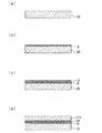
図1は、インクジェットヘッドの一例の要部、すなわちヘッド用チップの要部を示す図であり、図1中符号1はインクジェットヘッドである。このインクジェットヘッド1は、インクジェット式プリンターなどに用いられるもので、インクを貯留する圧力室2と、該圧力室2に設けられて前記インクを吐出するためのノズル3と、前記圧力室2の内圧を変化させ、前記ノズル3から該圧力室2内のインクを吐出させるためのアクチュエーター4と、を備えて構成されたものである。Hereinafter, the present invention will be described in detail.
First, prior to the description of the method for producing an inkjet head of the present invention, an example of an inkjet head obtained by this method will be described.
FIG. 1 is a diagram illustrating a main part of an example of an ink jet head, that is, a main part of a head chip, and
また、このインクジェットヘッド1は、圧力室2側を構成する下部構造体5と、アクチュエーター4側を構成する上部構造体6と、を有した略直方体状のヘッド用チップ(図示せず)を、一個又は複数個備えて構成されたものである。ここで、前記ヘッド用チップには、アクチュエーター4が多数(例えば180個×2列、又は360個×2列)形成されており、さらに圧力室2が、これらアクチュエーター4に対して1:1に対応して形成されている。 The
下部構造体5は、好ましくはニッケル(Ni)等の金属やその合金からなる略直方体状のもので、前記したように多数の圧力室2を有し、さらにインクジェットヘッド1の底面側に、前記ノズル3を形成したノズルプレート7を貼設したものである。なお、この下部構造体5については、Ni等の金属やその合金以外にも、シリコンや各種セラミックス、ガラス等から形成することもできる。ここで、圧力室2は、下部構造体5を上下に貫通して形成された空間であり、前記したようにその底面(下面)側がノズルプレート7に覆われ、後述するようにその上面側が上部構造体6の振動板9に覆われたことにより、ノズル孔、インク供給口以外は閉じられた状態に形成されたものである。 The
このような圧力室2は、インクジェットヘッド1の底面側を示す斜視図である図2に示すように、二列に整列した状態で多数配設されており、その底面側がノズルプレート7によって覆われ、閉じられている。ノズルプレート7に形成された多数のノズル3は、それぞれ圧力室2内に連通する位置に配置され、かつ二列に整列した状態で配置されている。
なお、図2では、簡略化して圧力室2を12個×2列で示したが、実際には、前述したように多数のアクチュエーター4に対応して、圧力室2も多数個形成されている。また、本実施例では2列で示しているが、必ずしも2列である必要はない。一列内で必要なノズル数、チップサイズ、必要な総ノズル数等を考慮し、都度適当な列数にすればよい。一般に列数を減らし、チップサイズを小型化すればアクチュエーターや圧力室の歩留まりは向上するが、ヘッドにチップを組み込む工程での煩雑さは増える。As shown in FIG. 2, which is a perspective view showing the bottom surface side of the
In FIG. 2, the
このような圧力室2は、図1では記載を省略しているものの、図2に示すように、圧力室2の配列方向に沿って形成された連通部8により連通している。そして、連通部8にはこれに連通してリザーバ(図示せず)が設けられ、このリザーバにはインク導入口(図示せず)が形成されている。このような構成のもとに圧力室2には、インクジェットヘッド1とは別に設けられたインクタンク(図示せず)より、チューブ(図示せず)を介して前記インク導入口にインクが供給され、さらにリザーバ、連通部8を経てインクが供給されるようになっている。 Although not shown in FIG. 1, such a
上部構造体6は、図1に示したように下部構造体5の上面側、すなわち前記ノズルプレート7と反対の側の面に接合されたものである。この上部構造体6は、その底面側に振動板9を有し、この振動板9の下面が前記下部構造体5に接合したことにより、下部構造体5に一体化されたものである。振動板9は、前述したように圧力室2の上面側を覆ってこれを閉じるもので、アクチュエーター4の駆動によって変位(撓曲)し、圧力室2の内圧を変化させるものである。 As shown in FIG. 1, the
このような振動板9は、酸化珪素(SiO2等のSiOx)と酸化ジルコニウム(ZrO2等のZrOx)との積層膜からなっている。すなわち、下部構造体5側に酸化珪素膜(図示せず)が配設され、その上に酸化ジルコニア膜(図示せず)が配設されたことにより、これら積層膜によって振動板9が構成されている。また、この振動板9は、厚さが例えば1〜2μm程度に形成されている。
振動板9の上には、前記アクチュエーター4が形成されている。アクチュエーター4は、前述したように圧力室2に1:1に対応して配設されたもので、図1に示したように、二列に整列した圧力室2のそれぞれの直上に配置され、したがってこれらアクチュエーター4も二列に整列したものとなっている。このアクチュエーター4は、本例では圧電体素子(ピエゾ素子)からなるもので、下部電極10と圧電体膜11と上部電極12とから構成されている。 The
下部電極10は、本例では前記振動板9上の全面に形成されたもので、厚さが例えば0.2μm程度の白金等によって形成されている。この下部電極10は、振動板9上の全面に形成されたことにより、アクチュエーター4の駆動によって振動板9とともに変位するようになっている。すなわち、この下部電極10は、アクチュエーター4の構成要素であるとともに、振動板9と同じ機能をも発揮するようになっている。なお、本例において下部電極10は、複数のアクチュエーター(圧電体素子)4の共通電極となっている。 In this example, the
圧電体膜11は、厚さが例えば1μm程度のPZT(Pb(Zr,Ti)O3)等によって形成されたものであり、上電極膜12は、厚さが例えば0.1μm程度の白金等によって形成されたものである。これら圧電体膜11と上部電極12とは、下部電極10と異なり、アクチューエーター4毎に独立して島状に形成されている。このような構成のもとにアクチュエーター4は、それぞれ独立して駆動するようになっている。The
これらアクチュエーター4上には、それぞれ保護膜13を介して配線14が接続されている。すなわち、前記下部電極10上には、前記圧電体膜11及び上部電極12を覆って酸化アルミニウム(Al2O3等のAlOx)等からなる保護膜13が形成されている。そして、この保護膜13には前記上部電極12に通じるコンタクトホール15が形成され、これにより、該配線14は、前記上部電極12に電気的に接続したものとなっている。A
また、このように振動板9、アクチュエーター4、配線14等が形成されてなる上部構造体6の上には、封止板16が貼設されており、これによって本例のインクジェットヘッド1が構成されている。この封止板16は、アクチュエーター部を保護する機能と、駆動制御用ICチップを配置することによる配線基板としての機能と、CMPをする際のウェハー支持基板の役割を果たす。また、封止板16に直接制御用ICを設けることなく、前記配線14から封止板16を経由してフレキシブル回路基板を外付けし、このフレキシブル回路基板(図示せず)にアクチュエーター4の駆動を制御する半導体装置を設けるようにしてもよい。 In addition, a sealing
このような構成からなるインクジェットヘッド1にあっては、アクチュエーター4に通電すると、圧電体膜11が圧電効果によってひずみ、変位することで外側に撓曲する。すると、下部電極10と振動板9とが圧電体膜11と一体になって同時に変位し、外側(封止板16側)へ撓曲することで、圧力室2内の容積を増大させ、内圧を低くする。
このようにして圧力室2内の容積が増大し、内圧が低下すると、連通部8を介して接続するリザーバ(図示せず)内にインクが充填されている場合には、増大した容積分に相当するインクが、リザーバから連通部8を介して圧力室2内に流入する。In the
When the volume in the
そして、このような状態からアクチュエーター4へそれまでと逆の電位を通電すると、圧力室2側に振動板9が撓むことにより圧力室2内の体積が減少し、内圧が高まる。これによってインクはノズル3から液滴となって吐出される。
なお、前記リザーバには、前述したようにインクジェットヘッド1とは別に設けられたインクタンク(図示せず)より、チューブ(図示せず)を介してインクが供給されるようになっている。When a reverse electric potential is applied to the
Note that ink is supplied to the reservoir via a tube (not shown) from an ink tank (not shown) provided separately from the
次に、このような構成からなるインクジェットヘッド1の製造方法に基づき、本発明のインクジェットヘッドの製造方法の一実施形態について説明する。
本発明が特に従来の製造方法と異なるところは、半導体プロセスにより下部構造体5と上部構造体6とを別個に形成し、それぞれ良品として判定されたものどうしを接合することにより、良品としてのインクジェットヘッド1を得る点にある。Next, based on the manufacturing method of the
The present invention is particularly different from the conventional manufacturing method in that the
すなわち、本実施形態では、まず図3(a)に示すようにシリコン基板(シリコンウエハ)20を用意する。ただし、従来では、KOHを用いた異方性エッチングでシリコン基板を直接加工し、圧力室を形成しているため、シリコン基板としては高価なSi(110)基板を用いる必要があったが、本発明では、後述するようにシリコン基板に圧力室を加工しないため、高価なSi(110)基板を用いる必要はなく、比較的安価な通常のSi(100)基板を用いることができる。 That is, in this embodiment, first, a silicon substrate (silicon wafer) 20 is prepared as shown in FIG. However, in the past, since a silicon substrate was directly processed by anisotropic etching using KOH to form a pressure chamber, an expensive Si (110) substrate had to be used as the silicon substrate. In the invention, since the pressure chamber is not processed in the silicon substrate as will be described later, it is not necessary to use an expensive Si (110) substrate, and a relatively inexpensive ordinary Si (100) substrate can be used.
そして、このシリコン基板20を熱酸化処理することにより、その表層部に酸化珪素(SiO2)膜を形成する。続いて、この酸化珪素膜上にスパッタ法でジルコニウム(Zr)を成膜する。次いで、これを熱酸化処理することにより、ジルコニウム膜から酸化ジルコニウム(ZrO2)膜を形成し、これによって図3(b)に示すように、酸化珪素膜と酸化ジルコニア膜との積層膜からなる振動板9を形成する。なお、酸化ジルコニア膜は、振動板の膜圧、剛性の調整と、この上部に形成する白金電極膜の配向制御と、さらに上層のPZTからの鉛の拡散が酸化珪素膜まで広がらないように止める拡散バリア層の役割を果たしている。振動板膜圧、剛性の調整の機能については、酸化珪素膜だけでも可能であり、電極成膜プロセスにより白金膜の配向制御が、電極により鉛拡散を防ぐことができれば、必ずしも酸化ジルコニア膜が必要ではない。Then, the
次いで、前記振動板9上にスパッタ法等の気相法によって白金を成膜し、図3(c)に示すように下部電極10を形成する。白金電極膜の製法としては、前記スパッタ法に限らず、蒸着法などの気相プロセスやめっき法のような液相プロセスでも可能である。なお、この下部電極10を成膜するに先立ち、酸化ジルコニア膜との間に接着層を形成する。一般にはTiOxでよいが、ZrOx等でもよい。
また、本実施形態では下部電極10として白金を用いているが、Irなどの金属や導電性酸化物電極、例えばSrRuO3やLaNiO3などでもよい。下部電極10には電極としての機能の他に、上部に形成する圧電体膜11の配向制御の機能も必要である。特に、(100)配向させたペロブスカイト構造の酸化物電極は、PZTの配向制御にもっとも都合がよい。
次いで、下部電極10上に、図3(d)に示すようにゾルゲル法等の液相法によってPZTからなる圧電体層11aを形成する。ここで、ゾルゲル法による圧電体層11aの形成方法としては、まず、PZTを構成する金属元素、すなわちPb、Zr、Tiを含有する化合物、例えばアルコキシド等の有機化合物を溶媒(分散媒)に溶解(分散)し、得られた溶液(分散液)を公知の塗布法で前記下部電極10上に配し、その後、焼成することによって圧電体層11aを得る、といった手法が採用される。なお、ゾルゲル法以外の手法として、例えばスパッタ法やCVD法、MOCVD法等の気相法や水熱合成法のような液相プロセスにより、圧電体層11aを形成するようにしてもよい。Next, a film of platinum is formed on the
In this embodiment, platinum is used as the
Next, as shown in FIG. 3D, a
次いで、圧電体層11a上にスパッタ法等の気相法によって白金を成膜し、図4(a)に示すように上部電極層12aを形成する。なお、上部電極12の成膜方法も下部電極10と同様、めっき等の液相法も可能であり、また必ずしも白金である必要はない。
このようにして下部電極10上に圧電体層11a及び上部電極層12aを形成したら、公知のレジスト技術、露光・現像技術によってレジストパターン(図示せず)を形成する。そして、このレジストパターンをマスクにして反応性イオンエッチング(RIE)等のドライエッチングを行い、上部電極層12a及び圧電体層11aをパターニングすることにより、図4(b)に示すように上部電極12及び圧電体膜11を形成する。これにより、圧電体素子からなるアクチュエーター4が得られる。Next, a film of platinum is formed on the
After the
ここで、上部電極層12a及び圧電体層11aのパターニングによるアクチュエーター4の形成に際しては、シリコン基板20上に、図5に示すように複数(例えば40個)のチップ領域21を設定する。そして、これら各チップ領域21毎に、予め設定した数のアクチュエーター4を、それぞれ二列に整列させた状態で形成する。なお、このようなアクチュエーター4の形成するためのエッチングにより、特に前記のチップ領域21についても、これを区画し、かつ隣り合うチップ領域21間を分ける溝状の境界部22を形成する。この境界部22の形成については、例えば振動板9中の酸化珪素までをエッチングし、シリコン基板20を露出させることで行う。 Here, when forming the
次いで、図4(c)に示すように前記シリコン基板20上に、スパッタ法等によってアクチュエーター4を覆って保護膜13を形成する。なお、この保護膜13は、PZTを外部環境(特に湿度)から保護するものであり、駆動時のアクチュエーターの撓みを妨げないよう、機能を果たせる範囲内で可能な限り薄いほうがよい。
次いで、レジストパターン(図示せず)を形成し、このレジストパターンをマスクにして前記保護膜13をエッチングすることにより、図4(d)に示すように前記上部電極12に通じるコンタクトホール15を形成する。Next, as shown in FIG. 4C, a
Next, a resist pattern (not shown) is formed, and the
一般に半導体チップの層間絶縁膜に形成したコンタクトホールの場合、アスペクト比が大きいため、タングステンプラグ等を形成する必要がある。ところが、本実施形態では前記層間絶縁膜にあたる保護膜の膜厚が100nm程度と薄く、またコンタクト径も数ミクロン以上となることから、コンタクトホールのアスペクト比が極めて小さい。このため、プラグを形成する必要なく、コンタクトホール形成後、直接配線層を形成することが可能である。 In general, a contact hole formed in an interlayer insulating film of a semiconductor chip has a large aspect ratio, so that it is necessary to form a tungsten plug or the like. However, in this embodiment, since the protective film corresponding to the interlayer insulating film is as thin as about 100 nm and the contact diameter is several microns or more, the aspect ratio of the contact hole is extremely small. For this reason, it is possible to form a wiring layer directly after forming a contact hole without forming a plug.
次いで、図6(a)に示すように保護膜13上にAl、Au等の配線材料を成膜して配線層14aを形成する。続いて、公知のレジスト技術、露光・現像技術、エッチング技術によって配線層14aをパターニングすることにより、図6(b)に示すように前記プラグに電気的に接続する配線14を形成する。 Next, as shown in FIG. 6A, a wiring material such as Al or Au is formed on the
このようにして各アクチュエーター4毎に配線14を接続したら、シリコン基板20上の全てのアクチュエーター4について電気的な検査を行い、さらに外観検査等を行うことにより、図5に示したチップ領域21毎に、その電気特性や外観についての良否を判定する。
次いで、必要に応じて前記配線14を覆う層間絶縁膜等(図示せず)を形成し、さらにシリコン基板20上の全面に、図6(c)に示すように封止板16を接着等により貼設する。これにより、シリコン基板20上には、図5に示した各チップ領域21毎に、上部構造体6が形成される。When the
Next, if necessary, an interlayer insulating film or the like (not shown) that covers the
次いで、シリコン基板20の底面側、すなわちアクチュエーター4を形成した側と反対の側を、化学機械研磨法(CMP法)で研磨し、図7(a)に示すように振動板9の底面側を露出させる。これにより、シリコン基板20を前記上部構造体から除去することができる。ここで、研磨量を制御し、特に振動板9における酸化珪素膜の研磨量を適宜に調整することにより、振動板9の厚さを所望の厚さに容易に制御することができる。 Next, the bottom surface side of the
その後、必要に応じてエッチングやダイシングを行うことにより、図5に示した各チップ領域21毎に分離し、図7(a)に示したように各チップ単位の上部構造体6を得る。
このようにして各チップ単位の上部構造体6を得たら、先に行った電気特性や外観についての検査結果より、良品と判定されたものを選別し、次工程に供するようにする。Thereafter, etching and dicing are performed as necessary to separate each
When the
一方、前記シリコン基板20を用いた工程とは別に、図7(b)に示すように圧力室2を有する下部構造体5を形成する。ここで、このようにして形成する下部構造体5としては、チップ単位となる構造のもの、すなわち、圧力室2を例えば180個×2列、又は360個×2列に形成したものを形成する。この下部構造体5の形成方法としては、特に、電鋳法が好適に用いられる。すなわち、予め下部構造体5の電鋳型を作製しておき、この電鋳型を陰極にして電解メッキを行い、電鋳型の内側に金属等を電着させることにより、下部構造体5を得る。電着させる金属等を、NiやNi合金とすることにより、これらNiやNi合金によって下部構造体5を形成する。このようにNiやNi合金によって下部構造体5を形成すれば、Ni又はNi合金は耐薬品性に優れ、比較的安価であるため、種々のインクに対して耐性のある圧力室2を安価に形成することができる。 On the other hand, separately from the process using the
なお、完成したインクジェットヘッド1において使用されるインクによっては、圧力室2内のインクと下部構造体5との間で化学反応等が生じ、電池効果が起きたり、腐蝕が起こる可能性もある。そのような場合には、予め圧力室2内(アクチュエーター振動板も同様)に例えば酸化タンタル(TaOx)等の保護膜を形成しておき、インクとの間の反応等を防止してもよい。
続いて、このようにして形成した下部構造体5について、外観検査等を行い、製品としての良否を判定する。そして、検査結果より良品と判定されたものを選別し、次工程に供するようにする。Depending on the ink used in the completed
Subsequently, an appearance inspection or the like is performed on the
次いで、良品として判定された上部構造体6と、良品として判定された下部構造体5とを組み合わせ、図7(c)に示すように上部構造体6の振動板9側と下部構造体5の上面側とを接合する。接合方法としては、加圧・加熱することで電子を拡散させることによる拡散接合や、水素接合、接合面をプラズマ処理することなどによって活性化させ、これら接合面同士を直接接合する直接接合、さらには、接着剤による接着などが採用可能である。 Next, the
その後、下部構造体5の底面側に、従来と同様にしてノズルプレート7を接着等で貼設し、ヘッド用チップ(図示せず)を得る。なお、このノズルプレート7の貼設については、上部構造体6と下部構造体5との接合に先立って行ってもよい。そして、このようにして形成したヘッド用チップを一個又は複数個用い、従来と同様にして組み立てることにより、図1に示したインクジェットヘッド1を得る。
このようにして得られたインクジェットヘッド1は、インクジェット式のプリンターや、工業用のインクジェット装置などに用いられる。Thereafter, the nozzle plate 7 is attached to the bottom surface side of the
The
このようなインクジェットヘッド1の製造方法にあっては、アクチュエーター4を含む上部構造体6と圧力室2を有する下部構造体5とをそれぞれ別に形成し、これらを接合してインクジェットヘッド1の構成要素となるヘッド用チップを形成するので、予め検査して良品と判定された上部構造体6と、別に検査して良品と判定された下部構造体5とを接合することで、前記ヘッド用チップの良品率(歩留まり)を上げ、その絶対数を十分に確保することができる。 In such a method of manufacturing the
すなわち、シリコン基板上にアクチュエーターやこれに接続する配線などを直接形成し、さらに同一のシリコン基板に圧力室も形成する従来法では、多くの工程を経てアクチュエーターや配線などを形成した後、圧力室を形成した際に、例えば異物や欠陥等に起因してこの圧力室に不良が発生すると、その上に形成された正常なアクチュエーターや配線なども、結果的に不良品の一部となってしまう。したがって、この正常なアクチュエーターや配線などは、最終的な製品に供されることができなくなり、そのため従来では歩留まりが大きく低下し、製造コストの低減化が妨げられていた。 That is, in the conventional method in which an actuator or wiring connected to the actuator is directly formed on a silicon substrate, and a pressure chamber is also formed on the same silicon substrate, the actuator and wiring are formed through many processes, and then the pressure chamber is formed. When a failure occurs in the pressure chamber due to, for example, foreign matter or a defect, a normal actuator or wiring formed thereon becomes a part of the defective product. . Therefore, these normal actuators and wirings cannot be used for final products, so that the yield has been greatly reduced in the past, and the reduction in manufacturing cost has been hindered.
これに対し、本発明にあっては、前述したように良品と判定された正常な上部構造体6は、同じく良品と判定された下部構造体5と接合されるようになるので、従来のごとく正常であるにもかかわらず不良品となってしまうといった不都合がなく、したがって、前述したように前記ヘッド用チップの良品率(歩留まり)が上がり、その絶対数も十分に確保できることにより、製造コストを低減化することができる。
また、高温プロセスを含むインクジェットヘッド1の上部構造体6の製造工程と、低温プロセスからなる下部構造体5の形成工程とを、連続させることなく別にしているので、工程管理が容易になり、したがって生産性の向上を図ることができる。On the other hand, in the present invention, the normal
In addition, since the manufacturing process of the
なお、本発明は前記実施形態に限定されることなく、本発明の要旨を逸脱しない限り種々の変更が可能である。例えば、前記実施形態ではアクチュエーターとして圧電体素子(ピエゾ素子)を用いたが、このような電気機械変換体以外の駆動素子をアクチュエーターとして用いることもできる。具体的には、エネルギー発生素子として電気熱変換体を用いた駆動素子や、帯電制御型、加圧振動型といった連続方式の駆動素子、静電吸引方式、さらにはレーザーなどの電磁波を照射して発熱させ、この発熱による作用で液状体を吐出させる方式の駆動素子などを採用することもできる。
また、下部構造体5の形成方法についても、電鋳法に限定されることなく、例えばナノインプリントによる転写技術を応用して形成することもできる。Note that the present invention is not limited to the above-described embodiment, and various modifications can be made without departing from the gist of the present invention. For example, in the above-described embodiment, a piezoelectric element (piezo element) is used as the actuator, but a driving element other than such an electromechanical transducer can also be used as the actuator. Specifically, a drive element using an electrothermal converter as an energy generation element, a continuous drive element such as a charge control type or a pressure vibration type, an electrostatic suction method, or an electromagnetic wave such as a laser is irradiated. It is also possible to employ a drive element that generates heat and discharges the liquid material by the action of the heat generation.
Further, the formation method of the
1…インクジェットヘッド、2…圧力室、3…ノズル、4…アクチュエーター、5…下部構造体、6…上部構造体、9…振動板、10…下部電極、11…圧電体膜、12…上部電極、20…シリコン基板、21…チップ領域、22…境界部
DESCRIPTION OF
Claims (6)
Translated fromJapanese基板上に液相法又は気相法を用いて前記アクチュエーターを形成し、上部構造体を製造する工程と、
前記基板から前記上部構造体を分離する工程と、
前記基板とは別に、圧力室を有する下部構造体を形成する工程と、
前記上部構造体と前記下部構造体とを接合する工程と、を備えたことを特徴とするインクジェットヘッドの製造方法。A pressure chamber for storing ink, a nozzle provided in the pressure chamber for discharging the ink, an actuator for changing the internal pressure of the pressure chamber and discharging the ink in the pressure chamber from the nozzle, In the manufacturing method of the ink-jet head comprising:
Forming the actuator on a substrate using a liquid phase method or a gas phase method, and manufacturing an upper structure;
Separating the upper structure from the substrate;
Forming a lower structure having a pressure chamber separately from the substrate;
And a step of bonding the upper structure and the lower structure.
In the step of separating the upper structure from the substrate, the upper structure is separated from the substrate by removing the upper structure from the upper structure by polishing the substrate by a chemical mechanical polishing method. The manufacturing method of the inkjet head as described in any one of Claims 1-5.
Priority Applications (2)
| Application Number | Priority Date | Filing Date | Title |
|---|---|---|---|
| JP2006067429AJP2007237718A (en) | 2006-03-13 | 2006-03-13 | Inkjet head manufacturing method |
| US11/684,809US20070220723A1 (en) | 2006-03-13 | 2007-03-12 | Method for manufacturing inkjet head |
Applications Claiming Priority (1)
| Application Number | Priority Date | Filing Date | Title |
|---|---|---|---|
| JP2006067429AJP2007237718A (en) | 2006-03-13 | 2006-03-13 | Inkjet head manufacturing method |
Publications (1)
| Publication Number | Publication Date |
|---|---|
| JP2007237718Atrue JP2007237718A (en) | 2007-09-20 |
Family
ID=38531805
Family Applications (1)
| Application Number | Title | Priority Date | Filing Date |
|---|---|---|---|
| JP2006067429APendingJP2007237718A (en) | 2006-03-13 | 2006-03-13 | Inkjet head manufacturing method |
Country Status (2)
| Country | Link |
|---|---|
| US (1) | US20070220723A1 (en) |
| JP (1) | JP2007237718A (en) |
Families Citing this family (4)
| Publication number | Priority date | Publication date | Assignee | Title |
|---|---|---|---|---|
| US8882221B2 (en)* | 2008-08-21 | 2014-11-11 | Funai Electric Co., Ltd. | Modular micro-fluid ejection head assembly |
| US20140187957A1 (en) | 2012-12-31 | 2014-07-03 | Volcano Corporation | Ultrasonic Transducer Electrode Assembly |
| JP6380890B2 (en)* | 2013-08-12 | 2018-08-29 | Tianma Japan株式会社 | Ink jet printer head, method for manufacturing the same, and drawing apparatus equipped with the ink jet printer head |
| JP6923010B2 (en)* | 2018-02-09 | 2021-08-18 | 株式会社村田製作所 | MEMS device |
Family Cites Families (11)
| Publication number | Priority date | Publication date | Assignee | Title |
|---|---|---|---|---|
| JPH09267494A (en)* | 1996-01-31 | 1997-10-14 | Sony Corp | Printer and its manufacture |
| EP0839653A3 (en)* | 1996-10-29 | 1999-06-30 | Matsushita Electric Industrial Co., Ltd. | Ink jet recording apparatus and its manufacturing method |
| JP3521708B2 (en)* | 1997-09-30 | 2004-04-19 | セイコーエプソン株式会社 | Ink jet recording head and method of manufacturing the same |
| US6322201B1 (en)* | 1997-10-22 | 2001-11-27 | Hewlett-Packard Company | Printhead with a fluid channel therethrough |
| US6266869B1 (en)* | 1999-02-17 | 2001-07-31 | Applied Kinetics, Inc. | Method for assembling components |
| JP2001010048A (en)* | 1999-07-01 | 2001-01-16 | Fujitsu Ltd | Ink jet head, method of manufacturing the same, and recording apparatus |
| JP3991894B2 (en)* | 2002-03-18 | 2007-10-17 | セイコーエプソン株式会社 | Piezoelectric actuator manufacturing method, liquid jet head manufacturing method, and actuator base member |
| JP3726909B2 (en)* | 2002-07-10 | 2005-12-14 | セイコーエプソン株式会社 | Method for manufacturing liquid jet head |
| JP4192794B2 (en)* | 2004-01-26 | 2008-12-10 | セイコーエプソン株式会社 | Piezoelectric element, piezoelectric actuator, ink jet recording head, ink jet printer, surface acoustic wave element, frequency filter, oscillator, electronic circuit, thin film piezoelectric resonator, and electronic device |
| US7347538B2 (en)* | 2004-03-23 | 2008-03-25 | Fujifilm Corporation | Method for manufacturing discharge head, and discharge head |
| JP4639724B2 (en)* | 2004-09-27 | 2011-02-23 | セイコーエプソン株式会社 | Method for manufacturing liquid jet head |
- 2006
- 2006-03-13JPJP2006067429Apatent/JP2007237718A/enactivePending
- 2007
- 2007-03-12USUS11/684,809patent/US20070220723A1/ennot_activeAbandoned
Also Published As
| Publication number | Publication date |
|---|---|
| US20070220723A1 (en) | 2007-09-27 |
Similar Documents
| Publication | Publication Date | Title |
|---|---|---|
| CN102632713B (en) | Inkjet head and image forming device | |
| JP6394903B2 (en) | Head and liquid ejecting apparatus | |
| JP5760475B2 (en) | Inkjet head | |
| CN100592982C (en) | Method of manufacturing actuator device, actuator device and liquid-jet head | |
| JP2011165916A (en) | Actuator, liquid droplet injection head, manufacturing method thereof, and droplet injecting aparatus | |
| JPH08118662A (en) | Printing head for ink jet printer and production thereof | |
| JP4640222B2 (en) | Inkjet head manufacturing method | |
| US7841056B2 (en) | Method of manufacturing a piezoelectric element | |
| JP5886723B2 (en) | Bonded silicon structures for high density printheads | |
| JP5309375B2 (en) | Ink jet print head and manufacturing method thereof | |
| CN212499504U (en) | Fluid ejection apparatus and system for fluid ejection | |
| JP4458052B2 (en) | Inkjet head manufacturing method | |
| JP2007237718A (en) | Inkjet head manufacturing method | |
| JP2009160923A (en) | Liquid ejecting head manufacturing method and liquid ejecting apparatus | |
| JP2011088311A (en) | Method of manufacturing actuator and method of manufacturing liquid ejection head | |
| JP2010214800A (en) | Manufacturing method for liquid droplet jetting head, and manufacturing method for piezoelectric element | |
| JP2008132733A (en) | Droplet discharge head, droplet discharge apparatus, and method of manufacturing droplet discharge head | |
| JP5569010B2 (en) | Inkjet head | |
| JP2006255972A (en) | Liquid ejecting head and liquid ejecting apparatus | |
| JP2009154433A (en) | Liquid jet head and manufacturing method thereof | |
| CN102950897B (en) | Liquid nozzle and manufacturing method thereof | |
| JP2010173197A (en) | Liquid discharge head, liquid discharge device, actuator device, and manufacturing method of liquid discharge head | |
| JP2009190349A (en) | Method for manufacturing liquid jet head | |
| JP2005096230A (en) | Method for manufacturing liquid jet head and liquid jet head | |
| JP2017209890A (en) | Inkjet recording head |
Legal Events
| Date | Code | Title | Description |
|---|---|---|---|
| A977 | Report on retrieval | Free format text:JAPANESE INTERMEDIATE CODE: A971007 Effective date:20091008 | |
| A131 | Notification of reasons for refusal | Free format text:JAPANESE INTERMEDIATE CODE: A131 Effective date:20091013 | |
| A521 | Written amendment | Free format text:JAPANESE INTERMEDIATE CODE: A523 Effective date:20091208 | |
| A521 | Written amendment | Free format text:JAPANESE INTERMEDIATE CODE: A821 Effective date:20091210 | |
| A02 | Decision of refusal | Free format text:JAPANESE INTERMEDIATE CODE: A02 Effective date:20100302 |