JP2007236061A - Overcurrent protective device - Google Patents
Overcurrent protective deviceDownload PDFInfo
- Publication number
- JP2007236061A JP2007236061AJP2006052587AJP2006052587AJP2007236061AJP 2007236061 AJP2007236061 AJP 2007236061AJP 2006052587 AJP2006052587 AJP 2006052587AJP 2006052587 AJP2006052587 AJP 2006052587AJP 2007236061 AJP2007236061 AJP 2007236061A
- Authority
- JP
- Japan
- Prior art keywords
- current
- turned
- control means
- fet
- overcurrent
- Prior art date
- Legal status (The legal status is an assumption and is not a legal conclusion. Google has not performed a legal analysis and makes no representation as to the accuracy of the status listed.)
- Pending
Links
- 230000001681protective effectEffects0.000titleabstract2
- 230000002265preventionEffects0.000claimsdescription16
- 238000001514detection methodMethods0.000claimsdescription15
- 230000005669field effectEffects0.000claimsdescription2
- 101100484930Saccharomyces cerevisiae (strain ATCC 204508 / S288c) VPS41 geneProteins0.000abstractdescription5
- 230000007257malfunctionEffects0.000abstractdescription5
- 239000003990capacitorSubstances0.000description12
- 238000000034methodMethods0.000description11
- 239000004065semiconductorSubstances0.000description11
- 238000010586diagramMethods0.000description6
- 230000000630rising effectEffects0.000description2
- 230000000694effectsEffects0.000description1
Images


Landscapes
- Emergency Protection Circuit Devices (AREA)
Abstract
Description
Translated fromJapanese本発明は、電子回路を過電流から保護する過電流防止装置に係り、特に、電流制御用の半導体素子が瞬間的な突入電流やノイズによって誤動作することを防止した過電流防止装置に関する。 The present invention relates to an overcurrent prevention device that protects an electronic circuit from overcurrent, and more particularly, to an overcurrent prevention device that prevents a semiconductor element for current control from malfunctioning due to an instantaneous inrush current or noise.
従来、過電流から高速で電子回路を保護する方法として、半導体スイッチを用いる方法がある。しかし、高速であるが故に瞬間的な突入電流やノイズであっても半導体スイッチが動作し、回路がオフとなってしまうという問題があった。これを防ぐ半導体スイッチの制御方法として、オン抵抗が異なる2つのMOSFETスイッチを並列に設け、過電流を検出した時、過電流フラグを出力し、スイッチをバイパス側に切り替えるようにして電流を即座に切断することなく。過電流を徐々に制御する方法が知られている(特許文献1)。 Conventionally, as a method for protecting an electronic circuit from an overcurrent at a high speed, there is a method using a semiconductor switch. However, because of the high speed, there is a problem that the semiconductor switch operates even if there is an instantaneous inrush current or noise, and the circuit is turned off. As a control method of the semiconductor switch to prevent this, two MOSFET switches with different on-resistances are provided in parallel, and when an overcurrent is detected, an overcurrent flag is output and the current is immediately switched by switching the switch to the bypass side. Without cutting. A method for gradually controlling overcurrent is known (Patent Document 1).
しかしながら、この方法は2つのMOSFETを用いているため、半導体スイッチが高価になる欠点があった。また、固定オン抵抗値を有するMOSFETとなっているため、瞬間的な電流であったとしても抵抗値が不足して電流を制限することができず、半導体スイッチが動作し、回路オフが継続してしまうという欠点があった。 However, since this method uses two MOSFETs, there is a drawback that the semiconductor switch is expensive. Moreover, since the MOSFET has a fixed on-resistance value, even if it is an instantaneous current, the resistance value is insufficient and the current cannot be limited, the semiconductor switch operates, and the circuit is kept off. There was a drawback that it would.
一方、過電流を検出すると、FETなどの半導体スイッチをオフとし、一定時間後に再度半導体スイッチがオンに復帰する制御を行い、一定時間で収束するような瞬間的な過電流であった場合には、誤動作を防止するという方法がある。しかしながら、瞬間的な過電流は、半導体スイッチがオフとなってから再度オンするまでの一定時間を超えるような場合には、スイッチオンとなっても過電流が収束していないため、再度、スイッチオフとなり、誤動作してしまう問題がある。 On the other hand, when an overcurrent is detected, the semiconductor switch such as an FET is turned off, and the semiconductor switch is controlled to turn on again after a certain time. There is a method of preventing malfunction. However, if the instantaneous overcurrent exceeds a certain time from when the semiconductor switch is turned off to when it is turned on again, the overcurrent has not converged even when the switch is turned on. There is a problem that it turns off and malfunctions.
また、瞬間的な過電流によりスイッチオフが継続しないように、半導体スイッチがオフとなってから再度オンとするまでの時間を長くすることができるが、逆に、長くなることにより、装置が瞬断してしまうという問題があった。
本発明は上記事情を考慮してなされたもので、その目的は、過電流から電子回路を保護することができ、しかも、瞬間的な突入電流やノイズによって誤動作することがない過電流防止装置を提供することにある。 The present invention has been made in consideration of the above circumstances, and an object of the present invention is to provide an overcurrent prevention device that can protect an electronic circuit from overcurrent and that does not malfunction due to instantaneous inrush current or noise. It is to provide.
この発明は上記の課題を解決するためになされたもので、請求項1に記載の発明は、保護対象の装置へ電流を供給する電流経路に挿入された電流制御手段と、前記電流経路を流れる電流を検出する電流検出手段と、前記電流検出手段によって検出された電流が所定の値を超えた時、前記電流制御手段を予め決められた一定時間オフとした後オンとし、所定時間内において前記電流制御手段のオン/オフの回数が一定値を越えた時、または、予め決められた一定時間前記電流制御手段のオン/オフが継続した時、前記電流検出手段を連続的にオフ状態とする制御手段とを具備することを特徴とする過電流防止装置である。 The present invention has been made to solve the above problems, and the invention according to
請求項2に記載の発明は、請求項1に記載の過電流防止装置において、前記制御手段は、電界効果トランジスタを備え、そのゲート電圧を制御して、前記電流経路を流れる電流が設定値以下となるように制御するゲート制御手段を有することを特徴とする
請求項3に記載の発明は、請求項1または請求項2に記載の過電流防止装置において、前記電流制御手段がオフとされた時、前記保護対象の装置へ電圧を供給する補償回路を設けたことを特徴とする。
請求項4に記載の発明は、請求項3に記載の過電流防止装置において、前記補償回路は、前記電流制御手段がオフとされた時、蓄えられている電圧を前記保護対象の装置へ供給する蓄電手段を有することを特徴とする。According to a second aspect of the present invention, in the overcurrent prevention device according to the first aspect, the control means includes a field effect transistor, and controls a gate voltage so that a current flowing through the current path is equal to or less than a set value The invention according to
According to a fourth aspect of the present invention, in the overcurrent prevention device according to the third aspect, the compensation circuit supplies the stored voltage to the protection target device when the current control means is turned off. It has the electrical storage means to perform.
この発明によれば、過電流から電子回路を保護することができ、しかも、瞬間的な突入電流やノイズによって誤動作することがない過電流防止装置を提供することができる。 According to the present invention, it is possible to provide an overcurrent prevention device that can protect an electronic circuit from an overcurrent and that does not malfunction due to an instantaneous inrush current or noise.
以下、図面を参照し、この発明の実施の形態について説明する。図1はこの発明の一実施の形態による過電流防止回路の構成を示すブロック図である。この図において、符号1は入力端子であり、電流制御手段2であるPチャネルMOSFET(電解効果トランジスタ)2のソースSに接続されている。FET2のドレインDは保護対象の電子回路が接続される出力端子3に接続され、ゲートGはゲート制御部(制御手段、ゲート制御手段)4に接続されている。5はFET2から出力端子3へ流れる電流Idを検出する電流検出部(電流検出手段)であり、常時、電流検出を行い、検出した電流値をゲート制御部4へ出力する。ゲート制御部4は、電流検出部5から出力される電流値に応じてFET2のゲート電圧を制御するものである。6は一端が出力端子3に接続された抵抗、7はカソードが出力端子3に接続されたダイオード、8は一端が抵抗6の他端およびダイオード7のアノードに接続され、他端が接地されたコンデンサ(蓄電手段)である。そしてこれらの抵抗6、ダイオード7、コンデンサ8によって、FET2がオフとなった時の出力電流を補償する補償回路9が構成されている。なお、補償回路9はFET2がオフで前記出力電流を補償して保護対象の装置へ電力を供給できるものであれば回路構成は特に限定されない。 Embodiments of the present invention will be described below with reference to the drawings. FIG. 1 is a block diagram showing a configuration of an overcurrent prevention circuit according to an embodiment of the present invention. In this figure,
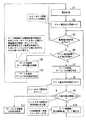
次に、上述したゲート制御部4の動作を図2に示すフローチャートを参照して説明する。
まず、初期状態においてFET2のゲートGへ接地電圧(0ボルト〔V〕)を印加する。これにより、FET2がオン状態となる。次に、電流Idの計測を行い(ステップS1)、ゲート電圧印加回数カウンタXを0クリアする(ステップS2)。次に、計測した電流値が予め設定されている電流値以下か否かを判定する(ステップS3)。そして、判定結果が設定値以下であった場合は、ステップS1へ戻り、電流検出部4から次の電流値が出力されるのを待つ。一方、判定結果が設定値以上であった場合、すなわち、過電流がFET2−出力端子3間に流れていた場合は、電流Idを規定値内に制限することが可能か否かを判定する(ステップS4)。電流Idを規定値以内に制限することが可能である場合には、ゲート制御部4はゲート印加電圧Pの演算を行い(ステップS5)、その演算した値をゲートGに印加して(ステップS6)、ステップS1の処理へ戻る。これは、ゲート制御部4には、ゲートGに印加する電圧と通過電流の関係である半導体の特性データが格納されており、電流値を設定値以下に制限するためにはゲートGに印加する電圧Pを何ボルト〔V〕にすればよいかを判定する。すなわち、負荷電流が増えたということは、負荷の抵抗が小さくなることから、所定の電流値とするためには、FET2のスイッチの抵抗を変えればよい。Next, the operation of the gate control unit 4 will be described with reference to the flowchart shown in FIG.
First, a ground voltage (0 volts [V]) is applied to the gate G of the
また、電流Idを規定値以内に制限することが可能である場合には、FET2のゲート電圧を徐々に上昇させることによってFET2のドレイン電流Idを制限して、ゲート制御部4はゲートGに入力電圧を印加し(ステップS7)、ゲート電圧印加回数カウンタXを1カウントアップする(ステップS8)。つぎに、ゲート電圧印加回数カウンタXが予め内部に設定されている設定回数n(例えば、10回等)以下か否かを判定する(ステップS9)。そして、該カウンタXの値が設定回数n以下であった場合は、瞬間的な過電流の可能性があると判定し、予め内部に設定されている時間t(例えば、1ミリセカンド〔msec〕)が経過後、FET2のゲート電圧を0ボルト〔V〕として(ステップS10)、ステップS3へ戻る。
一方、FET2のオフ回数Xが設定回数n以上となった場合は(ステップS9の判定が「NO」)、瞬間的な過電流ではないと判定し、以後、FET2のゲート電圧を入力電圧に保持する(ステップS11)。When the current Id can be limited within the specified value, the gate control unit 4 inputs the gate G by limiting the drain current Id of the
On the other hand, when the number of OFFs X of the
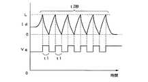
ここで、図3に示すゲート制御部4の波形図について説明する。
このように、ゲート制御部4は、電流Idが一定レベルLを越えると、ゲート電圧Vgを入力電圧としてFET2をオフとし、一定時間tの経過を待つ。時間tが経過した後、再びゲート電圧を接地電圧(0ボルト〔V〕)としてFET2をオンとし、電流Idが再びレベルLに達するか、あるいは越えると、再びゲート電圧Vgを入力電圧としてFET2をオフとし、時間tの経過を待ってFET2をオンとし、この動作を繰り返す。
そして、ゲート電圧Vgの立ち上がり回数が設定回数n回以上となった場合に、瞬間的な過電流ではないと判定し、FET2を継続的にオフ状態とする。また、ゲート電圧Vgの立ち上がり回数がn回以下で正常に戻れば(電流IdがレベルL以下になれば)、以後、FET2のオン状態を継続する。Here, a waveform diagram of the gate control unit 4 shown in FIG. 3 will be described.
As described above, when the current Id exceeds a certain level L, the gate control unit 4 turns off the
When the number of rising times of the gate voltage Vg becomes equal to or more than the set number n, it is determined that there is no instantaneous overcurrent, and the
補償回路9は、FET2がオフとされた時、出力端子3の電圧を補償するもので、通常時において抵抗6を介してコンデンサ8が充電され、FET2のオフ時にコンデンサ8に蓄えられた電圧がダイオード7を介して出力端子3に供給され、これにより、出力端子3の電圧が補償される(図1参照)。 The
なお、上記の実施形態において、過電流を検出すると瞬時にFET2のゲート電圧を入力電圧へ変化させてFET2をオフとしてもよい。また、瞬間的な突入電流やノイズによって信号を送出しないように、任意の検出不感時間を設定してもよい。
また、FET2をオンとする場合に、徐々にゲート電圧を接地電圧に変化させて、電流Idを徐々に上昇させる設定をしてもよく、また、ゲート電圧を瞬時に接地電池へ変化させ、FET2をオンとしてもよい。In the above embodiment, the
Further, when the
また、FET2としてnチャネルMOSFETを用いてもよい。
また、上記補償回路9として、図4(a)、(b)に示す回路を用いてもよい。
図4(a)に示す回路は、抵抗11、スイッチ12、13およびコンデンサ14によって構成され、通常時はスイッチ12がオンとなって抵抗11を介してコンデンサ14が充電され、過電流となった際にはFET2がオフの時はスイッチ13がオンとなって出力端子3へコンデンサ14の電圧が供給される。Further, an n-channel MOSFET may be used as the FET2.
Further, as the
The circuit shown in FIG. 4A is composed of a
図4(b)に示す回路は、トランジスタ15、抵抗16〜18およびコンデンサ19、20によって構成されている。そして、コンデンサ20の充電時は、バイパス抵抗16を介して突入電流が防止される。また、トランジスタ15はコンデンサ20の電圧に応じてターンオンする。つまり、概念的には図4(c)に示すように、トランジスタ15のベースには、((R1/R1+R2)・Vc)ボルト〔V〕が印加され、トランジスタ15のエミッタEにはコンデンサ20(図4(b)参照)の充電電圧(初期値は0ボルト〔V〕)が印加される。 The circuit shown in FIG. 4B includes a
また、上記実施形態においては、時間tの間FET2をオフとし、オフ回数が設定回数n回に達した時点以降、FET2を連続的にオフとしたが、これに代えて、次のように制御してもよい。すなわち、図5に示すように、FET2のオフの持続時間をt1とし、FET2のオン/オフの繰り返し時間が予め設定した時間t2に達した時点以降、FET2を連続的にオフとする。例えば、FET2の通過電流が0から過電流検出値になるまでの時間を1ミリセカンド〔msec〕とし、また、時間t1を1ミリセカンド〔msec〕、時間t2を20ミリセカンド〔msec〕とすると、結局、10回オン/オフを繰り返した後、FET2を連続的にオフとすることになる。
FET2の通過電流が0から過電流検出値になるまでの時間は、短絡箇所までの配線インピーダンスに依存する。配線インピーダンスが大きい場合、電流の増加時間が長く、配線インピーダンスが小さい場合、電流の増加時間が短くなる。立ち上がり回数がn回設定の場合、上記条件によって、過電流を遮断するまでの時間は短絡箇所によって様々であり、一定ではない。上述した図5の制御方法は、設定された任意の時間以内に過電流を遮断したいという時に有効な設定方法である。Further, in the above embodiment, the
The time required for the passing current of the
この発明は、電子回路の過電流防止に用いられる。 The present invention is used to prevent overcurrent of electronic circuits.
1…入力端子
2…FET(電流制御手段)
3…出力端子
4…ゲート制御部(制御手段、ゲート制御手段)
5…電流検出部(電流検出手段)
6、11、16〜18…抵抗
7…ダイオード
8、14、19、20…コンデンサ(蓄電手段)
9…補償回路
DESCRIPTION OF
3 ... Output terminal 4 ... Gate control section (control means, gate control means)
5 ... Current detection part (current detection means)
6, 11, 16-18 ...
9. Compensation circuit
Claims (4)
Translated fromJapanese前記電流経路を流れる電流を検出する電流検出手段と、
前記電流検出手段によって検出された電流が所定の値を超えた時、前記電流制御手段を予め決められた一定時間オフとした後オンとし、所定時間内において前記電流制御手段のオン/オフの回数が一定値を越えた時、または、予め決められた一定時間前記電流制御手段のオン/オフが継続した時、前記電流検出手段を連続的にオフ状態とする制御手段と、
を具備することを特徴とする過電流防止装置。Current control means inserted in a current path for supplying current to the device to be protected;
Current detecting means for detecting a current flowing through the current path;
When the current detected by the current detection means exceeds a predetermined value, the current control means is turned off after being turned off for a predetermined time, and the number of times the current control means is turned on / off within the predetermined time. Control means for continuously turning off the current detection means when the current control means continues on / off for a predetermined time period when
An overcurrent prevention device comprising:
4. The overcurrent prevention device according to claim 3, wherein the compensation circuit includes a power storage unit that supplies a stored voltage to the device to be protected when the current control unit is turned off.
Priority Applications (1)
| Application Number | Priority Date | Filing Date | Title |
|---|---|---|---|
| JP2006052587AJP2007236061A (en) | 2006-02-28 | 2006-02-28 | Overcurrent protective device |
Applications Claiming Priority (1)
| Application Number | Priority Date | Filing Date | Title |
|---|---|---|---|
| JP2006052587AJP2007236061A (en) | 2006-02-28 | 2006-02-28 | Overcurrent protective device |
Publications (1)
| Publication Number | Publication Date |
|---|---|
| JP2007236061Atrue JP2007236061A (en) | 2007-09-13 |
Family
ID=38556085
Family Applications (1)
| Application Number | Title | Priority Date | Filing Date |
|---|---|---|---|
| JP2006052587APendingJP2007236061A (en) | 2006-02-28 | 2006-02-28 | Overcurrent protective device |
Country Status (1)
| Country | Link |
|---|---|
| JP (1) | JP2007236061A (en) |
Cited By (10)
| Publication number | Priority date | Publication date | Assignee | Title |
|---|---|---|---|---|
| JP2009201316A (en)* | 2008-02-25 | 2009-09-03 | Autonetworks Technologies Ltd | Vehicular power supply |
| JP2011217498A (en)* | 2010-03-31 | 2011-10-27 | Ntt Facilities Inc | Semiconductor breaker and dc power supply system |
| JP2011217497A (en)* | 2010-03-31 | 2011-10-27 | Ntt Facilities Inc | Semiconductor breaker and dc power supply system |
| JP2012004870A (en)* | 2010-06-17 | 2012-01-05 | Nippon Telegr & Teleph Corp <Ntt> | Breaking device |
| JP2012039861A (en)* | 2010-08-10 | 2012-02-23 | Krohne Messtechnik Gmbh | Energy supply device |
| JP2012145363A (en)* | 2010-11-03 | 2012-08-02 | Easymore Industrial Co Ltd | Failure detection and protection circuit of dc power supply system |
| JP2012531184A (en)* | 2009-06-26 | 2012-12-06 | リバティー ハードウェア マニュファクテュアリング コーポレイション | System and method for protecting a circuit |
| JP2013513348A (en)* | 2009-12-04 | 2013-04-18 | ローベルト ボツシユ ゲゼルシヤフト ミツト ベシユレンクテル ハフツング | Elements that limit the current in electrical circuits |
| DE102020216405A1 (en) | 2020-12-21 | 2022-06-23 | Siemens Aktiengesellschaft | Method for driving a power semiconductor switch, driving circuit for a power semiconductor switch and electronic circuit breaker |
| CN116191383A (en)* | 2023-03-06 | 2023-05-30 | 江苏吉泰科电气有限责任公司 | Overcurrent protection method and circuit |
- 2006
- 2006-02-28JPJP2006052587Apatent/JP2007236061A/enactivePending
Cited By (13)
| Publication number | Priority date | Publication date | Assignee | Title |
|---|---|---|---|---|
| JP2009201316A (en)* | 2008-02-25 | 2009-09-03 | Autonetworks Technologies Ltd | Vehicular power supply |
| JP2012531184A (en)* | 2009-06-26 | 2012-12-06 | リバティー ハードウェア マニュファクテュアリング コーポレイション | System and method for protecting a circuit |
| JP2013513348A (en)* | 2009-12-04 | 2013-04-18 | ローベルト ボツシユ ゲゼルシヤフト ミツト ベシユレンクテル ハフツング | Elements that limit the current in electrical circuits |
| JP2011217498A (en)* | 2010-03-31 | 2011-10-27 | Ntt Facilities Inc | Semiconductor breaker and dc power supply system |
| JP2011217497A (en)* | 2010-03-31 | 2011-10-27 | Ntt Facilities Inc | Semiconductor breaker and dc power supply system |
| JP2012004870A (en)* | 2010-06-17 | 2012-01-05 | Nippon Telegr & Teleph Corp <Ntt> | Breaking device |
| JP2012039861A (en)* | 2010-08-10 | 2012-02-23 | Krohne Messtechnik Gmbh | Energy supply device |
| JP2012145363A (en)* | 2010-11-03 | 2012-08-02 | Easymore Industrial Co Ltd | Failure detection and protection circuit of dc power supply system |
| DE102020216405A1 (en) | 2020-12-21 | 2022-06-23 | Siemens Aktiengesellschaft | Method for driving a power semiconductor switch, driving circuit for a power semiconductor switch and electronic circuit breaker |
| US12074591B2 (en) | 2020-12-21 | 2024-08-27 | Siemens Aktiengesellschaft | Method for actuating a semiconductor power switch, actuation circuit for a semiconductor power switch, and electronic circuit breaker |
| DE102020216405B4 (en) | 2020-12-21 | 2025-10-02 | Siemens Aktiengesellschaft | Method for controlling a power semiconductor switch, control circuit for a power semiconductor switch and electronic circuit breaker |
| CN116191383A (en)* | 2023-03-06 | 2023-05-30 | 江苏吉泰科电气有限责任公司 | Overcurrent protection method and circuit |
| CN116191383B (en)* | 2023-03-06 | 2023-09-29 | 江苏吉泰科电气有限责任公司 | An overcurrent protection method and circuit |
Similar Documents
| Publication | Publication Date | Title |
|---|---|---|
| JP2007236061A (en) | Overcurrent protective device | |
| JP5274823B2 (en) | Power supply control circuit | |
| JP5590031B2 (en) | Power supply protection circuit and motor drive device including the same | |
| JP5135214B2 (en) | Inrush current control system and method with soft start circuit | |
| US8488289B2 (en) | Current protection circuit for intelligent power switch | |
| JP5274815B2 (en) | Power supply control circuit | |
| CN112054662A (en) | Electronic safety device for a power supply device | |
| US20170256938A1 (en) | Semiconductor device | |
| US10205313B2 (en) | Two-transistor devices for protecting circuits from sustained overcurrent | |
| EP1456925B1 (en) | A polarity protection implemented with a mosfet | |
| JP4263685B2 (en) | Protection circuit | |
| US7015681B2 (en) | Power switching circuit with current sharing capability | |
| CA2525820C (en) | Two wire touch sensor interface | |
| US5488533A (en) | Methods and apparatus for isolating a power network from a load during an overcurrent condition | |
| EP3731413A1 (en) | Gate driver circuit and method for driving a gate of a field-effect transistor | |
| JP5361242B2 (en) | Inrush current reduction circuit | |
| US20200212671A1 (en) | Electronic circuit breaker and method for operating same | |
| JP6519498B2 (en) | Switching power supply | |
| JP2005312099A (en) | Intelligent power device and load short circuit protection method thereof | |
| EP2783381B1 (en) | A method and circuit for increasing the speed of an electromechanical output on a protective relay | |
| JP4900321B2 (en) | Overcurrent protection circuit | |
| KR100815481B1 (en) | Overcurrent protection circuit and method | |
| JP2010017063A (en) | Electronic equipment | |
| JP2007336620A (en) | Power supply input circuit | |
| US20150130383A1 (en) | Method for discharging energy stored in a stator of an electric motor |
Legal Events
| Date | Code | Title | Description |
|---|---|---|---|
| A621 | Written request for application examination | Free format text:JAPANESE INTERMEDIATE CODE: A621 Effective date:20080731 | |
| A977 | Report on retrieval | Effective date:20090703 Free format text:JAPANESE INTERMEDIATE CODE: A971007 | |
| A131 | Notification of reasons for refusal | Effective date:20090707 Free format text:JAPANESE INTERMEDIATE CODE: A131 | |
| A02 | Decision of refusal | Effective date:20091104 Free format text:JAPANESE INTERMEDIATE CODE: A02 |